MAX14819 Dal IOLink Master Transceiver it Integrate raers ... · raers an L+ Spply Controllers...
70
General Description The MAX14819 low-power, dual-channel, IO-Link ® master transceiver with sensor/actuator power-supply controllers is fully compliant with the latest IO-Link and binary input standards and test specifications, IEC 61131-2, IEC 61131-9 SDCI, and IO-Link 1.1.2. This master transceiver also includes two auxiliary digital input (DI_) channels. The MAX14819 is configurable to operate either with external UARTs or using the integrated framers on the IC. To ease selection of microcontroller, the master transceiver features frame handlers with UARTs and FIFOs. These are designed to simplify time critical control of all IO-Link M-sequence frame types. The MAX14819 also features autonomous cycle timers, reducing the need for accu- rate controller timing. Integrated establish-communication sequencers also simplify wake-up management. The MAX14819 integrates two low-power sensor supply controllers with advanced current limiting, reverse current-blocking, and reverse polarity protection capability to enable low-power robust solutions. The MAX14819 is available in a 48-pin (7mm x 7mm) TQFN package and is specified over the extended -40°C to +125°C temperature range. Applications ● IO-Link Master Systems ● IO-Link Gateways Benefits and Features ● Low-Power Architecture • 1Ω (typ) Driver On-Resistance • 1.9mA (typ) Total Supply Current for 2 Channels • Current Limiters with 15mV Sense Voltage ● Integrated IO-Link Framer Eliminates Need for External UARTs • Integrated Cycle Timer Relieves Microcontroller from Timing-Critical Tasks ● High Configurability and Integration Reduce SKUs • Two Auxiliary Type 1/Type 3 Digital Inputs • Supports NPN Sensors • Dual 24V Sensor Supply Controllers Include: • Large Capacitive Load Charge Capability • 2A and Higher Load Currents ● Integrated Protection Enables Robust Systems • Reverse Polarity Protection on All Interface Pins • Overvoltage Tolerance on All Interface Pins • C/Q and DI Fully Compliant with IEC 61131-2 • C/Q Compliant with IO-Link 1.1.2 • Reverse Current Blocking on L+ and C/Q • 65V Absolute Max Ratings for TVS Flexibility • Glitch Filters for Improved Burst Resilience • -40°C to +125°C Operating Temperature Range Ordering Information appears at end of data sheet. IO-Link is a registered trademark of Profibus User Organization (PNO). 19-8744; Rev 1; 8/17 10µF 24V 1µF VL V5 VCC G1A SN1A SN2A G2A L+A 330pF XI XO CLKO CLKI A0 A1 GND MAX14819 µC SPI 14.7456MHz CQA DIA REGEN TXA TXENA THE MAX14819 IS A DUAL-CHANNEL MASTER TRANSCEIVER. ONLY ONE CHANNEL IS SHOWN HERE. OPERATED WITH INTERNAL IO-LINK FRAMER. 3.3V RXRDYA/LD1A RXERRA/LD2A MAX12930 MAX14931 IRQ 3.3V 5V 3.3V 100Ω 100Ω 1µF MAX14819 Dual IO-Link Master Transceiver with Integrated Framers and L+ Supply Controllers Typical Operating Circuit EVALUATION KIT AVAILABLE
-
Upload
hoangkhanh -
Category
Documents
-
view
214 -
download
0
Transcript of MAX14819 Dal IOLink Master Transceiver it Integrate raers ... · raers an L+ Spply Controllers...
General DescriptionThe MAX14819 low-power, dual-channel, IO-Link® master transceiver with sensor/actuator power-supply controllers is fully compliant with the latest IO-Link and binary input standards and test specifications, IEC 61131-2, IEC 61131-9 SDCI, and IO-Link 1.1.2. This master transceiver also includes two auxiliary digital input (DI_) channels.The MAX14819 is configurable to operate either with external UARTs or using the integrated framers on the IC.To ease selection of microcontroller, the master transceiver features frame handlers with UARTs and FIFOs. These are designed to simplify time critical control of all IO-Link M-sequence frame types. The MAX14819 also features autonomous cycle timers, reducing the need for accu-rate controller timing. Integrated establish-communication sequencers also simplify wake-up management.The MAX14819 integrates two low-power sensor supply controllers with advanced current limiting, reverse current-blocking, and reverse polarity protection capability to enable low-power robust solutions. The MAX14819 is available in a 48-pin (7mm x 7mm) TQFN package and is specified over the extended -40°C to +125°C temperature range.
Applications IO-Link Master Systems IO-Link Gateways
Benefits and Features Low-Power Architecture • 1Ω(typ)DriverOn-Resistance • 1.9mA (typ) Total Supply Current for 2 Channels• Current Limiters with 15mV Sense Voltage
Integrated IO-Link Framer Eliminates Need for External UARTs• Integrated Cycle Timer Relieves Microcontroller
from Timing-Critical Tasks
High Configurability and Integration Reduce SKUs• Two Auxiliary Type 1/Type 3 Digital Inputs• Supports NPN Sensors• Dual 24V Sensor Supply Controllers Include:
• Large Capacitive Load Charge Capability• 2A and Higher Load Currents
Integrated Protection Enables Robust Systems • Reverse Polarity Protection on All Interface Pins• Overvoltage Tolerance on All Interface Pins• C/Q and DI Fully Compliant with IEC 61131-2• C/Q Compliant with IO-Link 1.1.2• Reverse Current Blocking on L+ and C/Q• 65V Absolute Max Ratings for TVS Flexibility• Glitch Filters for Improved Burst Resilience• -40°C to +125°C Operating Temperature Range
Ordering Information appears at end of data sheet.
IO-Link is a registered trademark of Profibus User Organization (PNO).
19-8744; Rev 1; 8/17
10µF
24V
1µF
VL V5 VCC G1A SN1A SN2A G2A L+A
330pFXI
XO
CLKO
CLKI A0 A1 GND
MAX14819
µC
SPI
14.7456MHz
CQA
DIA
REGEN
TXA TXENA
THE MAX14819 IS A DUAL-CHANNEL MASTER TRANSCEIVER. ONLY ONE CHANNEL IS SHOWN HERE. OPERATED WITH INTERNAL IO-LINK FRAMER.
3.3V
RXRDYA/LD1ARXERRA/LD2A
MAX12930
MAX14931
IRQ
3.3V
5V3.3V
100Ω
100Ω
1µ F
MAX14819 Dual IO-Link Master Transceiver with Integrated Framers and L+ Supply Controllers
Typical Operating Circuit
EVALUATION KIT AVAILABLE
CQA
V5
DRIVER
DIA
DIB
SN2A G2AG1A
SDI
SCLKSDO
CHANNEL B
VL
L+ SUPPLY CONTROLLER
REGMAX14819
SPI REGISTERS
FRAME HANDLER
CHANNEL A
XTAL OSCILLATOR
CYCLE TIMER
XI
XO
CLKO
SN1B
RXA
TXA
RXB
TXB
TXENA
TXENB
CS
LIALIB
SYNC
A0A1
G2BSN2BG1B SN1AREGEN VCC
GND
L+B
L+A
CLKI
RXRDYA/LD1A
IRQ
RXERRB/LD2B
RXERRA/LD2A
RXRDYB/LD1B
ESTABLISHCOMM
CQB
MAX14819 Dual IO-Link Master Transceiver with Integrated Framers and L+ Supply Controllers
www.maximintegrated.com Maxim Integrated 2
Functional Diagram

(All voltages referenced to GND, unless otherwise noted.)VCC ............................max [(VPM - 70V), (VCQ_ - 70V)] to +65V V5, VL ......................................................................-0.3V to +6VREGEN ............................. -0.3V to the min(VCC + 0.3V or +6V)CQA, CQB .................................................. (VCC - 70V) to +65VDIA, DIB, L+A, L+B .................................... (VPM - 70V) to +65VSN1A, SN1B ..........................................................-0.3V to +65VSN2A ..................................... (VSN1A - 0.3V) to (VSN1A + 0.3V)SN2B ..................................... (VSN1B - 0.3V) to (VSN1B + 0.3V)G1A, G2A ...........max (-0.3V, [VSN1A - 14V]) to (VSN1A + 0.3V) G1B, G2B ...........max (-0.3V, [VSN1B - 14V]) to (VSN1B + 0.3V)XI, XO .......................................................... -0.3V to (V5 + 0.3V)VPM ............. max (0V, VCC, DIA, DIB, SN1A, SN1B, L+A, L+B)
Logic Inputs CS, SDI, SCLK, A_, TXEN_, TX_, CLKI ... -0.3V to (VL + 0.3V)
Logic Outputs SDO, IRQ, LI_, RX_, RXRDY_/LD1_, RXERR_/LD2_, CLKO ............................ -0.3V to (VL + 0.3V)
Continuous Current Into GND and VCC ................................±2AContinuous Current Into CQA and CQB ...............................±1AContinuous Current Into V5 ............................................±100mAContinuous Current Into Any Other Pin ............................±50mAContinuous Power Dissipation
TQFN (derate 40mW/°C above +70°C) ...........................3.2WOperating Temperature Range ......................... -40°C to +125°CMaximum Junction Temperature ......................Internally LimitedStorage Temperature Range ............................ -65°C to +150°CSoldering Temperature (reflow) .......................................+260°C
Multilayer Board Junction-to-AmbientThermalResistance(θJA) ..............25°C/W Junction-to-CaseThermalResistance(θJC) .....................1°C/W
(Note 1)
(VCC = 9V to 36V, V5 = 4.5V to 5.5V, VL = 1.62V to 5.5V, VGND = 0V, all logic inputs at VL or GND; TA = -40°C to +125°C, unless otherwise noted. Typical values are at VCC = 24V, V5 = 5V, VL = 3.3V, and TA = +25°C, unless otherwise noted.) (Note 2)
PARAMETER SYMBOL CONDITIONS MIN TYP MAX UNITSVCC POWERVCC Supply Voltage VCC 9 36 VVCC Undervoltage-Lockout Threshold VCCUVLO VCC rising 7 9 V
VCC Undervoltage-Lockout-Threshold Hysteresis VCCUVLO_HYST 340 mV
VCC Supply Current ICC
REGEN = GND, L+EnA = L+EnB = 1, external clock selected, CQ_ in push-pull configuration,CL[1:0] = 00, no load on CQ_
CQ_ outputs low 0.4 0.75
mA
CQ_ outputs high 0.5 0.85
VCC Warning Threshold VCC_WRN 16 18 V
VCC Warning Threshold Hysteresis VCC_WHY 500 mV
MAX14819 Dual IO-Link Master Transceiver with Integrated Framers and L+ Supply Controllers
www.maximintegrated.com Maxim Integrated 3
Note 1: Package thermal resistances were obtained using the method described in JEDEC specification JESD51-7, using a four-layer board. For detailed information on package thermal considerations, refer to www.maximintegrated.com/thermal-tutorial.
Absolute Maximum Ratings
Stresses beyond those listed under “Absolute Maximum Ratings” may cause permanent damage to the device. These are stress ratings only, and functional operation of the device at these or any other conditions beyond those indicated in the operational sections of the specifications is not implied. Exposure to absolute maximum rating conditions for extended periods may affect device reliability.
Package Thermal Characteristics
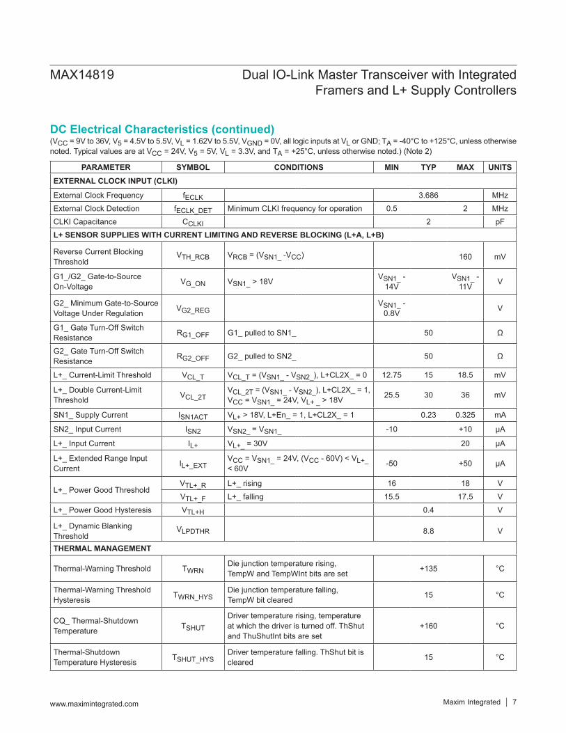
DC Electrical Characteristics

(VCC = 9V to 36V, V5 = 4.5V to 5.5V, VL = 1.62V to 5.5V, VGND = 0V, all logic inputs at VL or GND; TA = -40°C to +125°C, unless otherwise noted. Typical values are at VCC = 24V, V5 = 5V, VL = 3.3V, and TA = +25°C, unless otherwise noted.) (Note 2)
PARAMETER SYMBOL CONDITIONS MIN TYP MAX UNITSV5 POWERV5 Supply Voltage V5 REGEN = GND 4.5 5 5.5 V
V5 Supply Current IV5
REGEN = GND, L+EnA = L+EnB = 1, external clock selected, CQ_ in push-pull configuration,CL[1:0] = 00, no load on CQ_
CQ_ outputs low 1.4 1.9
mA
CQ outputs high 1.4 1.9
V5 LINEAR REGULATOR
V5 Output Voltage V5REGEN unconnected, no load on V5, CQ_ disabled, L+EnA = L+EnB = 0 4.75 5.25 V
V5 Current Limit ICL_V5REGEN unconnected, CQ_ disabled, L+EnA = L+EnB = 0 20 mA
V5 Load Regulation dVV5
REGEN unconnected, CQ_ disabled, L+EnA=L+EnB=0,0mA≤ILOAD≤20mA
-0.1 mV/mA
REGEN Pullup Current IREGEN VREGEN = 0V 5 30 μA
REGEN Threshold VTH_REGEN 0.2 1.8 2.6 V
VL POWER
VL Logic-Level Supply Voltage VL 1.62 5.5 V
VL Undervoltage Threshold VLUVLO VL falling 0.4 1.5 V
VL Undervoltage Threshold Hysteresis VLUVHYS 50 mV
VL Logic-Level Supply Current IL
All logic inputs at VL or GND, all logic outputs unconnected 5 µA
CQ_ DRIVER
Driver On-Resistance ROH High-side enabled, ILOAD = -200mA 1.0 2
ΩROL Low-side enabled, ILOAD = +200mA 1.0 2.2
Driver Current Limit ICLVCQ_ = (VCC - 3V) or 3V
CL[1:0] = 00 100 150
mACL[1:0] = 01 190 280
CL[1:0] = 10 280 410
CL[1:0] = 11 500 650
MAX14819 Dual IO-Link Master Transceiver with Integrated Framers and L+ Supply Controllers
www.maximintegrated.com Maxim Integrated 4
DC Electrical Characteristics (continued)

(VCC = 9V to 36V, V5 = 4.5V to 5.5V, VL = 1.62V to 5.5V, VGND = 0V, all logic inputs at VL or GND; TA = -40°C to +125°C, unless otherwise noted. Typical values are at VCC = 24V, V5 = 5V, VL = 3.3V, and TA = +25°C, unless otherwise noted.) (Note 2)
PARAMETER SYMBOL CONDITIONS MIN TYP MAX UNITSCQ_, DI_ RECEIVER
CQ_, DI_ Input Threshold High VTH CQ_ driver disabled
IEC3Th_/DiEC3Th = 0
10.5 13.0
VIEC3Th_/DiEC3Th = 1
7.5 11.0
CQ_, DI_ Input Threshold Low VTL CQ_ driver disabled
IEC3Th_/DiEC3Th = 0
8.0 11.5V
IEC3Th_ /DiEC3Th = 1 6.0 8.0
CQ_, DI_ Input Threshold Hysteresis VHYS CQ_ driver disabled
IEC3Th_/DiEC3Th= 0
2V
IEC3Th_/DiEC3Th= 1
2
CQ_ Current Sink ICQ_SNKVCQ_ > 5V,
SourceSink_ = 0
2mA pulldown enabled(SinkSel_[1:0] = 10)
2 2.5 2.75
mA5mA pulldown enabled(SinkSel_[1:0] = 01)
5 5.8 6.6
CQ_ Current Source ICQ_SRC(VCC - VCQ_) > 5V,
SourceSink_ = 1
2mA pullup enabled(SinkSel_[1:0] = 10)
-2.75 -2.5 -2
mA5mA pullup enabled(SinkSel_[1:0] = 01)
-6.6 -5.8 -5
CQ_ Weak Pulldown Current ICQ_PD
Driver disabled (DrvDis_ = 1), SourceSink = 0, weak pulldown enabled (SinkSel_[1:0] = 11), VCQ_ > 5V
150 250 μA
CQ_ Weak Pullup Current ICQ_PU
Driver disabled (DrvDis_ = 1), SourceSink = 1, weak pullup enabled (SinkSel_[1:0] = 11), VCC - VCQ_ > 5V
-250 -150 μA
CQ_ Input Current ICQ
CQ_ driver enabled (DrvDis = 0), CQ_set to high impedance, pullup and pulldown disabled (SinkSel_[1:0] = 00), receiver enabled, VCC = 24V, -1V < VCQ_ < (VCC + 1V)
-60 +400 μA
CQ_ Input Current, Extended Range ICQ_EXT
CQ_ driver enabled (DrvDis = 0), CQ_set to high impedance, pullup and pulldown disabled (SinkSel_[1:0] = 00), receiver enabled, VCC = 24V, (VCC - 65V) < VCQ_ < 60V
-200 +500 μA
MAX14819 Dual IO-Link Master Transceiver with Integrated Framers and L+ Supply Controllers
www.maximintegrated.com Maxim Integrated 5
DC Electrical Characteristics (continued)

(VCC = 9V to 36V, V5 = 4.5V to 5.5V, VL = 1.62V to 5.5V, VGND = 0V, all logic inputs at VL or GND; TA = -40°C to +125°C, unless otherwise noted. Typical values are at VCC = 24V, V5 = 5V, VL = 3.3V, and TA = +25°C, unless otherwise noted.) (Note 2)
PARAMETER SYMBOL CONDITIONS MIN TYP MAX UNITS
CQ_ Leakage Current ICQ_LKG
CQ_ driver disabled (DrvDis = 1), pullup and pulldown disabled (SinkSel_[1:0] = 00), receiver enabled, VCC = 24V, (VCC - 65V) < VCQ_ < 60V
-100 +100 μA
CQ_ Push-Pull High Impedance Current ICQ_HiZ
CQ_ driver enabled (DrvDis = 0), CQ_in push-pull, pullup and pulldown disabled (SinkSel_[1:0] = 00), receiver enabled, VCC = 24V, 0V < VCQ_ < 24V
-50 +50 μA
DI_ Current Sink IDI_SNK VDI_ > 5V, DiCSink = 1 2 2.5 3 mA
DI_ Current Source IDI_SRC VCC - VDI_ > 5V, DiCSource = 1 -3 -2.5 -2 mA
DI_ Input Current IDI
Pullup and pulldown disabled, DI_ receiver enabled, VCC = 24V, -1V < VDI_ < (VCC + 1V)
-5 +50 μA
DI_ Input Current, Extended Range IDI_EXT
Pullup and pulldown disabled, DI_ receiver enabled, VCC = 24V, (VCC - 65V) < VDI_ < 60V
-100 +100 μA
LOGIC INPUTS (CS, SDI, SCLK, A1, A0, TXENA, TXENB, TXA, TXB, CLKI)Logic Input Voltage Low VIL 0.2 x VL V
Logic Input Voltage High VIH 0.8 x VL V
Logic Input Leakage Current ILEAK Logic input = GND or VL -1 +1 µA
LOGIC OUTPUTS (SDO, IRQ, LIA, LIB, RXA, RXB, RXRDYA/LD1A, RXERRA/LD2A, RXRDYB/LD1B, RXERRB/LD2B, CLKO)Logic Output Voltage Low VOL IOUT = -5mA 0.4 V
Logic Output Voltage High VOH RX_, LI_, SDO, and CLKO, IOUT = 5mA VL - 0.4 V
Output Leakage Current IOH
RXRDY_/LD1_, RXERR_/LD2_, IRQ, output is high impedance, output is pulled up to 5V
-1 +1 µA
CRYSTAL OSCILLATOR (XI, XO)Crystal Oscillator Current Supply IV5_XTAL
fXTAL = 14.7456MHz, V5 supply current increase versus external clocking 240 µA
Crystal Equivalent Series Resistance ESRXTAL fXTAL = 14.7456MHz (Note 4) 75 Ω
Crystal Shunt Capacitance COXTAL fXTAL = 14.7456MHz (Note 4) 8 pF
Input Capacitance CINXI 10
pFXO 10
INTERNAL OSCILLATOR
Internal Oscillator Current Consumption IV5_OSC (Notes 3, 5) 55 µA
MAX14819 Dual IO-Link Master Transceiver with Integrated Framers and L+ Supply Controllers
www.maximintegrated.com Maxim Integrated 6
DC Electrical Characteristics (continued)
(VCC = 9V to 36V, V5 = 4.5V to 5.5V, VL = 1.62V to 5.5V, VGND = 0V, all logic inputs at VL or GND; TA = -40°C to +125°C, unless otherwise noted. Typical values are at VCC = 24V, V5 = 5V, VL = 3.3V, and TA = +25°C, unless otherwise noted.) (Note 2)
PARAMETER SYMBOL CONDITIONS MIN TYP MAX UNITSEXTERNAL CLOCK INPUT (CLKI)
External Clock Frequency fECLK 3.686 MHz
External Clock Detection fECLK_DET Minimum CLKI frequency for operation 0.5 2 MHz
CLKI Capacitance CCLKI 2 pF
L+ SENSOR SUPPLIES WITH CURRENT LIMITING AND REVERSE BLOCKING (L+A, L+B)
Reverse Current Blocking Threshold
VTH_RCB VRCB = (VSN1_ -VCC) 160 mV
G1_/G2_ Gate-to-Source On-Voltage VG_ON VSN1_ > 18V VSN1_ -
14VVSN1_ -
11V V
G2_ Minimum Gate-to-Source Voltage Under Regulation VG2_REG
VSN1_ - 0.8V V
G1_ Gate Turn-Off Switch Resistance RG1_OFF G1_ pulled to SN1_ 50 Ω
G2_ Gate Turn-Off Switch Resistance RG2_OFF G2_ pulled to SN2_ 50 Ω
L+_ Current-Limit Threshold VCL_T VCL_T = (VSN1_ - VSN2_), L+CL2X_ = 0 12.75 15 18.5 mV
L+_ Double Current-Limit Threshold VCL_2T
VCL_2T = (VSN1_ - VSN2_), L+CL2X_ = 1, VCC = VSN1_ = 24V, VL+ _ > 18V 25.5 30 36 mV
SN1_ Supply Current ISN1ACT VL+ > 18V, L+En_ = 1, L+CL2X_ = 1 0.23 0.325 mA
SN2_ Input Current ISN2 VSN2_ = VSN1_ -10 +10 μA
L+_ Input Current IL+ VL+_ = 30V 20 μA
L+_ Extended Range Input Current IL+_EXT
VCC = VSN1_ = 24V, (VCC - 60V) < VL+_ < 60V -50 +50 μA
L+_ Power Good ThresholdVTL+_R L+_ rising 16 18 V
VTL+_F L+_ falling 15.5 17.5 V
L+_ Power Good Hysteresis VTL+H 0.4 V
L+_ Dynamic Blanking Threshold
VLPDTHR 8.8 V
THERMAL MANAGEMENT
Thermal-Warning Threshold TWRNDie junction temperature rising, TempW and TempWInt bits are set +135 °C
Thermal-Warning Threshold Hysteresis TWRN_HYS
Die junction temperature falling, TempW bit cleared 15 °C
CQ_ Thermal-Shutdown Temperature TSHUT
Driver temperature rising, temperature at which the driver is turned off. ThShut and ThuShutInt bits are set
+160 °C
Thermal-Shutdown Temperature Hysteresis TSHUT_HYS
Driver temperature falling. ThShut bit is cleared 15 °C
MAX14819 Dual IO-Link Master Transceiver with Integrated Framers and L+ Supply Controllers
www.maximintegrated.com Maxim Integrated 7
DC Electrical Characteristics (continued)

(VCC = 18V to 30V, V5 = 4.5V to 5.5V, VL = 1.62V to 5.5V, VGND = 0V; TA = -40°C to +125°C, unless otherwise noted. Typical values are at VCC = 24V, V5 = 5V, VL = 3.3, and TA = +25°C, unless otherwise noted.) (Note 2)
PARAMETER SYMBOL CONDITIONS MIN TYP MAX UNITSCQ_ DRIVER
Driver Low-to-High Propagation Delay tPDLH
Push-pull and PNP Figure 1 0.27 0.5μsNPN Figure 1
(no capacitive load) 2.16
Driver High-to-Low Propagation Delay tPDHL
Push-pull and NPN Figure 1 0.44 0.5μsPNP Figure 1
(no capacitive load) 0.3
Driver Skew tSKEW |tPDLH - tPDHL|, Figure 1 0.15 μs
Driver Rise Time tRISE Push-pull and PNP Figure 1 0.18 0.4 μs
Driver Fall Time tFALL Push-pull and NPN Figure 1 0.18 0.4 µs
Driver Enable Time High tENH Push-pull and PNP Figure 2 0.25 0.5 µs
Driver Enable Time Low tENL Push-pull and NPN Figure 3 0.15 0.5 µs
Driver Disable Time High tDISH Push-pull and PNP Figure 2 1.9 3 µs
Driver Disable Time Low tDISL Push-pull and NPN Figure 3 1.7 3 µs
CQ_ RECEIVER (Figure 4)
CQ_ Receiver Low-to-High Propagation Delay tCPRLH
CQFilterEn_ = 0 0.28 0.5µs
CQFilterEn_ = 1 1.2 2
CQ_ Receiver High-to-Low Propagation Delay tCPRHL
CQFilterEn_ = 0 0.25 0.5µs
CQFilterEn_ = 1 1.2 2
CQ_ Receiver Skew tCRSKEW |tCPRLH - tCPRHL|CQFilterEn_ = 0 0.1 µs
CQFilterEn_ = 1 0.1 µsDI_ RECEIVER (Figure 4)
DI_ Receiver Low-to-High Propagation Delay tDPRLH
DiFilterEn = 0 1.9 3µs
DiFilterEn = 1 2.9 4.2
DI_ Receiver High-to-Low Propagation Delay tDPRHL
DiFilterEn = 0 1.3 3µs
DiFilterEn = 1 2.3 4.2
DI_ Receiver Skew tDRSKEW|tDPRLH - tDPRHL|, DiFilterEn_ = 0 0.5 1 µs
|tDPRLH - tDPRHL|, DiFilterEn_ = 1 0.5 1 µs
WAKE-UP PULSEDelay Time to Wake-Up Pulse tSU_WU (Figure 9) 80 µs
Wake-Up Pulse Duration tWU
Wake-up (WU) pulse has the opposite polarity of the CQ_ line before the WU pulse was generated
75 80 85 µs
On-Time After Wake-Up tON_WUDriver enabled with original polarity on CQ_ line 100 µs
MAX14819 Dual IO-Link Master Transceiver with Integrated Framers and L+ Supply Controllers
www.maximintegrated.com Maxim Integrated 8
AC Electrical Characteristics
(VCC = 18V to 30V, V5 = 4.5V to 5.5V, VL = 1.62V to 5.5V, VGND = 0V; TA = -40°C to +125°C, unless otherwise noted. Typical values are at VCC = 24V, V5 = 5V, VL = 3.3, and TA = +25°C, unless otherwise noted.) (Note 2)
PARAMETER SYMBOL CONDITIONS MIN TYP MAX UNITSL+ CURRENT LIMITING
Reverse Current Blocking Response Time
tRCBDelay between (VRCB rising > VTH_RCB) and IGATE2_ turned off 10 μs
Reverse Current Blocking Threshold VTH_RCB VRCB = (VSN1_ - VCC) 160 mV
Current-Limit Blanking Time tL+CLBL
L+BL_[1:0] = 00 5 5.5
msL+BL_[1:0] = 01 15 16.5
L+BL_[1:0] = 10 50 55
L+BL_[1:0] = 11 150 165
Current-Limit Retry Delay tL+CLRT
L+RT_[1:0] = 00, latched off ∞
sL+RT_[1:0] = 01 0.5
L+RT_[1:0] = 10 4
L+RT_[1:0] = 11 10
CYCLE TIMER
Cycle Time tCYCL
Actual cycle time relative to programmed cycle time, using an external clock or crystal with 100ppm accuracy
0 4 5 %
SPI TIMING (CS, SCLK, SDI, SDO) (Figure 5)
Maximum SPI Clock Frequency1.6V≤VL < 2.5V 15.6
MHz VL≥2.5V 20
SCLK Clock Period tCH+CL1.6V≤VL < 2.5V 64
ns VL≥2.5V 50
SCLK Pulse-Width High tCH1.6V≤VL < 2.5V 32
ns VL≥2.5V 25
SCLK Pulse-Width Low tCL1.6V≤VL < 2.5V 32
ns VL≥2.5V 25
CS Fall to SCLK Rise Time tCSS1.6V≤VL < 2.5V 10
ns VL≥2.5V 7
SDI Hold Time tDH1.6V≤VL < 2.5V 0
ns VL≥2.5V 0
SDI Setup Time tDS1.6V≤VL < 2.5V 25
nsVL≥2.5V 23
SDO Output Data Propagation Delay tDO
1.6V≤VL < 2.5V 35ns
VL≥2.5V 15
SDO Rise and Fall Times tFTVL = 1.8V 1.4
ns VL≥2.5V 0.7
MAX14819 Dual IO-Link Master Transceiver with Integrated Framers and L+ Supply Controllers
www.maximintegrated.com Maxim Integrated 9
AC Electrical Characteristics (continued)
Note 2: All devices are 100% production tested at TA = +25°C. Limits over the operating temperature range are guaranteed by design.
Note 3: Not production tested. Guaranteed by design.Note 4: Includes stray capacitance or resistance. Required characteristic of the external crystal. Note 5: V5 supply current increases when the internal oscillator is selected.
(VCC = 18V to 30V, V5 = 4.5V to 5.5V, VL = 1.62V to 5.5V, VGND = 0V; TA = -40°C to +125°C, unless otherwise noted. Typical values are at VCC = 24V, V5 = 5V, VL = 3.3, and TA = +25°C, unless otherwise noted.) (Note 2)
PARAMETER SYMBOL CONDITIONS MIN TYP MAX UNITS
Minimum CS Pulse High tCSW1.6V≤VL < 2.5V 10
ns VL≥2.5V 10
CS Hold Time tCSH1.6V≤VL < 2.5V 32 VL≥2.5V 25
MAX14819 Dual IO-Link Master Transceiver with Integrated Framers and L+ Supply Controllers
www.maximintegrated.com Maxim Integrated 10
AC Electrical Characteristics (continued)

Figure 1. C/Q Driver Propagation Delays and Rise/Fall Times
TX_
GND
CQ_
TXEN_
MAX14819
5kΩ3.3nF
TX_
GND
CQ_
TXEN_
MAX14819
5kΩ
3.3nF
VCC
PUSH-PULL AND PNP MODE NPN MODE
TX_
CQ_
tPDHL
tFALL
90%
10%50%
TXEN_
0V
VL
0V
VL
0V
VCC90%
10%50%
tRISE
tPDLH
50% 50%
TX_
CQ_
tPDHL
tRISE
90%
10%50%
TXEN_
0V
VL
0V
VL
0V
VCC90%
10%50%
tFALL
tPDLH
50% 50%
(a) INVCQ_ = 0
(b) INVCQ_ = 1
MAX14819 Dual IO-Link Master Transceiver with Integrated Framers and L+ Supply Controllers
www.maximintegrated.com Maxim Integrated 11
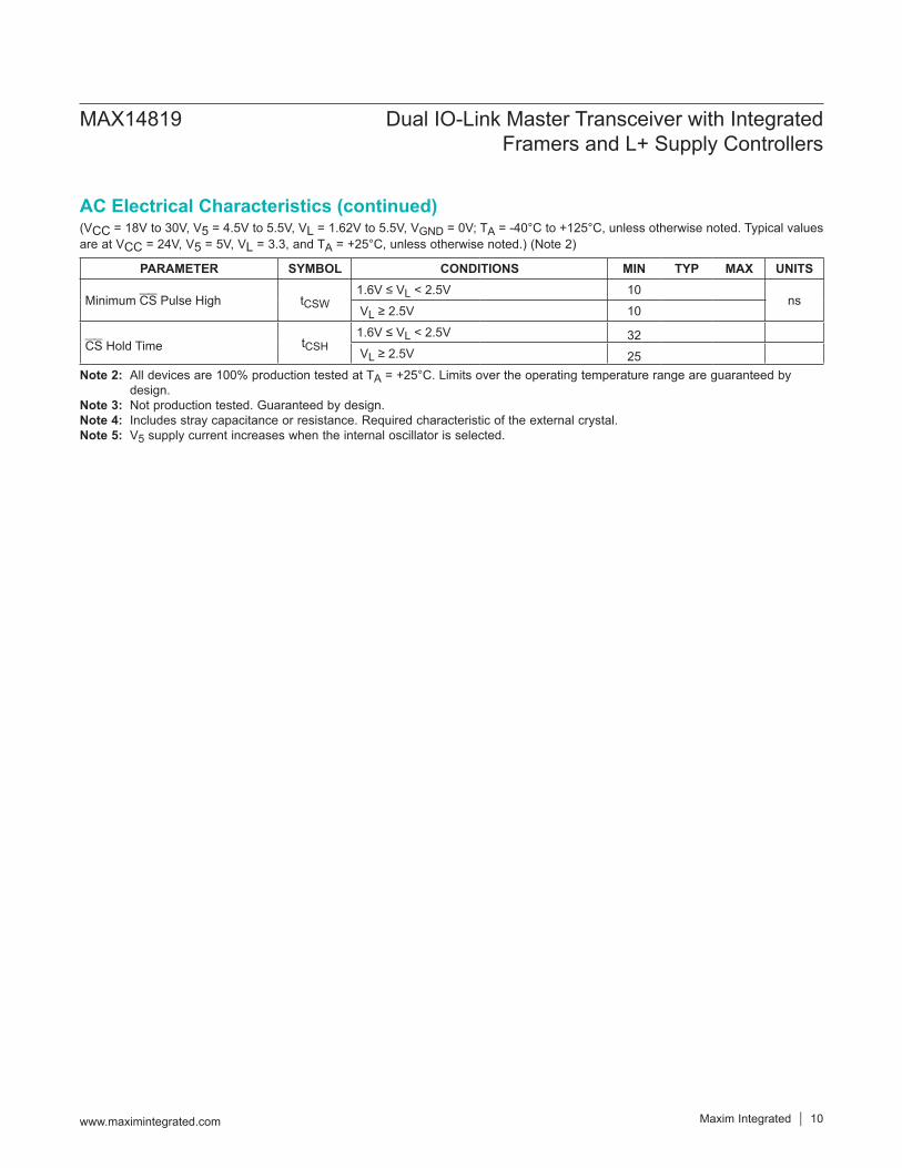
Figure 2. C/Q Driver Enable Low and Disable High Timing with External Pullup Resistor (INVCQ_ = 0)
Figure 3. C/Q Driver Enable High and Disable Low Timing (INVCQ_ = 0)
TXEN_
CQ_
tENL
10%50%
TXEN_
GND
TX_
VL
VL
0V
VCC
0V
5kΩ
3.3nF
VCC
MAX14819
tDISH
CQ_
TXEN_
CQ_
tENH
90%50%
TXEN_
GND
TX_
VL
0V
VCC
0V
5kΩ3.3nF
MAX14819
tDISL
CQ_
MAX14819 Dual IO-Link Master Transceiver with Integrated Framers and L+ Supply Controllers
www.maximintegrated.com Maxim Integrated 12

Figure 4. C/Q Receiver Propagation Delays
CQ_ OR DI_
GND
RX_ OR LI_
TXEN_
15pF
MAX14819
CQ_ OR DI_
RX_ OR LI_
tPRLH
tPRHL
50%
50%
VCC
0V
VL
0V
50%
50%
CQ_ OR DI_
RX_ OR LI_
tPRLH
tPRHL
50%
50%
VCC
0V
VL
0V
50%
50%
(a) INVCQ_ = 0
(a) INVCQ_ = 1
MAX14819 Dual IO-Link Master Transceiver with Integrated Framers and L+ Supply Controllers
www.maximintegrated.com Maxim Integrated 13

Figure 5. SPI Timing Diagram
tCSH tCLtCSS tCH tCSH
CS
SCLK
SDI
SDO
tDStDH
tDO
MAX14819 Dual IO-Link Master Transceiver with Integrated Framers and L+ Supply Controllers
www.maximintegrated.com Maxim Integrated 14
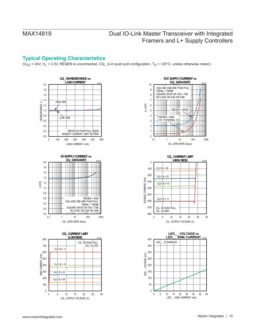
(VCC = 24V, VL=3.3V,REGENisunconnected,CQ_isinpush-pullconfiguration,TA = +25°C, unless otherwise noted.)
0
1
2
3
4
5
6
7
8
9
10
0.1 1 10 100 1000
I CC
(mA)
CQ_ DATA RATE (kbps)
VCC SUPPLY CURRENT vsCQ_ DATA RATE
REGEN = OPEN
toc02
REGEN = GND, V5 = EXTERNAL 5V
CQA AND CQB ARE PUSH PULLTXENA = TXENBSQUARE WAVE ON TXA = TXBNO LOAD ON CQA OR CQB
0.0
0.2
0.4
0.6
0.8
1.0
1.2
1.4
1.6
1.8
2.0
0.1 1 10 100 1000
I 5(m
A)
CQ_ DATA RATE (kbps)
V5 SUPPLY CURRENT vs CQ_ DATA RATE toc03
REGEN = GNDCQA AND CQB ARE PUSH PULL
TXENA = TXENBSQUARE WAVE ON TXA = TXB
NO LOAD ON CQA OR CQB-800
-700
-600
-500
-400
-300
-200
-100
0
0 5 10 15 20 25 30
SOUR
CE C
URRE
NT (
mA)
CQ_ OUTPUT VOLTAGE (V)
CQ_ CURRENT LIMIT (HIGH SIDE) toc04
CL[1:0] = 00
CL[1:0] = 01
CL[1:0] = 10
CL[1:0] = 11
CQ_ IN PUSH PULLCQ_ IS HIGH
0.0
0.2
0.4
0.6
0.8
1.0
1.2
1.4
1.6
1.8
2.0
0 100 200 300 400 500 600
ON-
RESI
STAN
CE (
Ω)
LOAD CURRENT (mA)
CQ_ ON-RESISTANCE vsLOAD CURRENT toc01
HIGH SIDE
LOW SIDE
DRIVER IN PUSH PULL MODEHIGHEST CURRENT LIMIT SETTING
0
100
200
300
400
500
600
700
800
0 5 10 15 20 25 30
SINK
CUR
RENT
(m
A)
CQ_ OUTPUT VOLTAGE (V)
CQ_ CURRENT LIMIT (LOW SIDE) toc05
CL[1:0] = 00
CL[1:0] = 01
CL[1:0] = 10
CL[1:0] = 11
CQ_ IN PUSH PULLCQ_ IS LOW
0
50
100
150
200
250
300
350
400
0 5 10 15 20 25 30 35 40
LED_
_ V
OLT
AGE
(mV)
LED_ _ SINK CURRENT (mA)
LED_ _ VOLTAGE vs LED_ _ SINK CURRENT toc06
LED_ _ IS ENABLED
MAX14819 Dual IO-Link Master Transceiver with Integrated Framers and L+ Supply Controllers
Maxim Integrated 15www.maximintegrated.com
Typical Operating Characteristics
(VCC = 24V, VL=3.3V,REGENisunconnected,CQ_isinpush-pullconfiguration,TA = +25°C, unless otherwise noted.)
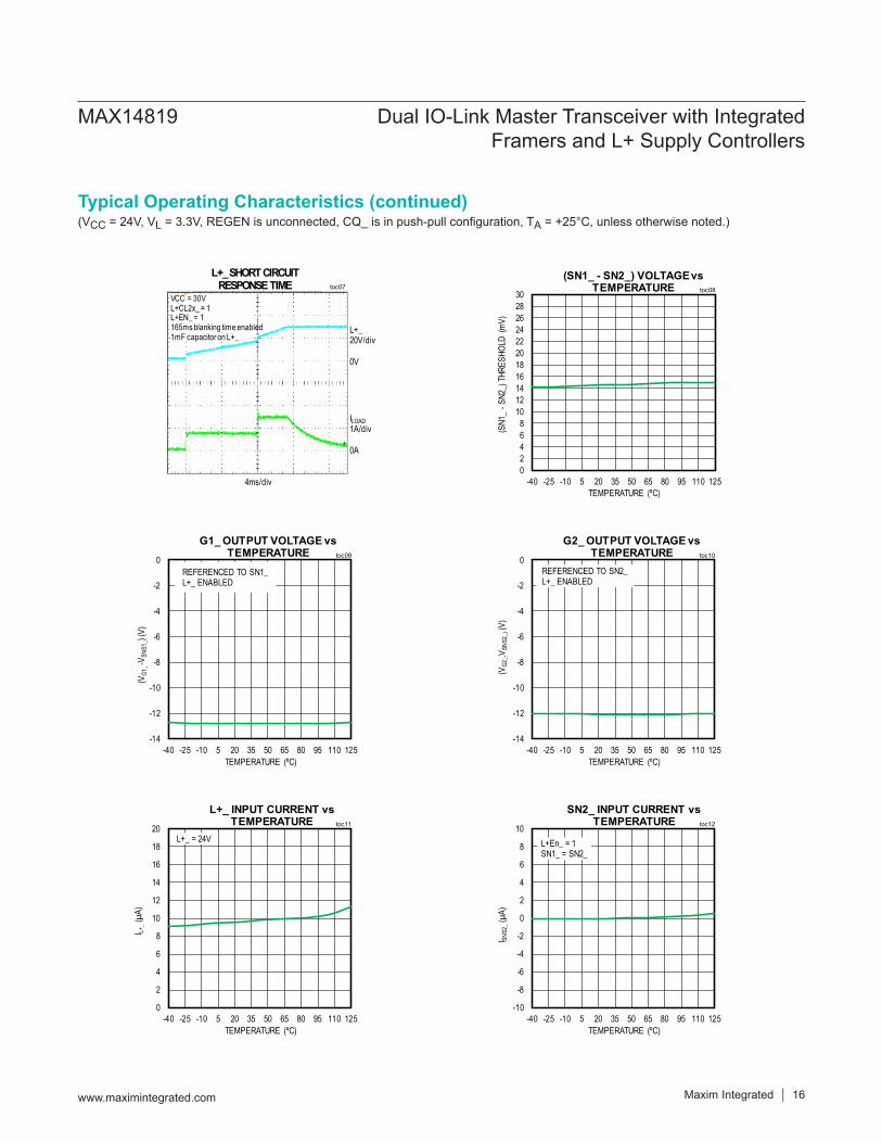
L+_ SHORT CIRCUIT RESPONSE TIME
L+_20V/div
0V
ILOAD1A/div
0A
toc07
4ms/div
VCC = 30VL+CL2x_ = 1L+EN_ = 1165ms blanking time enabled1mF capacitor on L+_
02468
1012141618202224262830
-40 -25 -10 5 20 35 50 65 80 95 110 125
(SN1
_ -S
N2_)
THR
ESHO
LD (
mV)
TEMPERATURE (ºC)
(SN1_ - SN2_) VOLTAGE vs TEMPERATURE toc08
-14
-12
-10
-8
-6
-4
-2
0
-40 -25 -10 5 20 35 50 65 80 95 110 125
(VG
1_ -V
SNS1
_)(V
)
TEMPERATURE (ºC)
G1_ OUTPUT VOLTAGE vs TEMPERATURE toc09
REFERENCED TO SN1_L+_ ENABLED
-14
-12
-10
-8
-6
-4
-2
0
-40 -25 -10 5 20 35 50 65 80 95 110 125
(VG
2_-V
SNS2
_)(V
)
TEMPERATURE (ºC)
G2_ OUTPUT VOLTAGE vs TEMPERATURE toc10
REFERENCED TO SN2_L+_ ENABLED
0
2
4
6
8
10
12
14
16
18
20
-40 -25 -10 5 20 35 50 65 80 95 110 125
I L+_
(µA)
TEMPERATURE (ºC)
L+_ INPUT CURRENT vs TEMPERATURE toc11
L+_ = 24V
-10
-8
-6
-4
-2
0
2
4
6
8
10
-40 -25 -10 5 20 35 50 65 80 95 110 125
I SNS2
_(µ
A)
TEMPERATURE (ºC)
SN2_ INPUT CURRENT vs TEMPERATURE toc12
L+En_ = 1SN1_ = SN2_
MAX14819 Dual IO-Link Master Transceiver with Integrated Framers and L+ Supply Controllers
Maxim Integrated 16www.maximintegrated.com
Typical Operating Characteristics (continued)
PIN NAME FUNCTION REFERENCE
1 IRQOpen-drain Interrupt Output. Connect a pullup resistor to IRQ. IRQ asserts whenever a bit that has been enabled in the InterruptEn register is set in the Interrupt register. See the Register Description for more information.
GND
2 RXRDYA/LD1A
ChannelAConfigurableOpen-DrainReceiveDataReadyOutput/LD1ADriver.Set the RxRdyEnA bit to 1 in the LEDCtrl register to enable RXRDYA/LD1A as aninterruptoutput.Inthisconfiguration,RXRDYA/LD1A asserts when the Rx-DataEnRdyA interrupt bit is set in the Interrupt register. Set the RxRdyA bit to 0 toconfigureRXRDYA/LD1Aasanopen-drainLEDdriver.Whenconfiguredasan LED driver, RXRDYA/LD1A is controlled by the LEDEn1A bit in the LEDCtrl register. Connect a resistor in series to limit the LED current. See the Register Description for more information.
GND
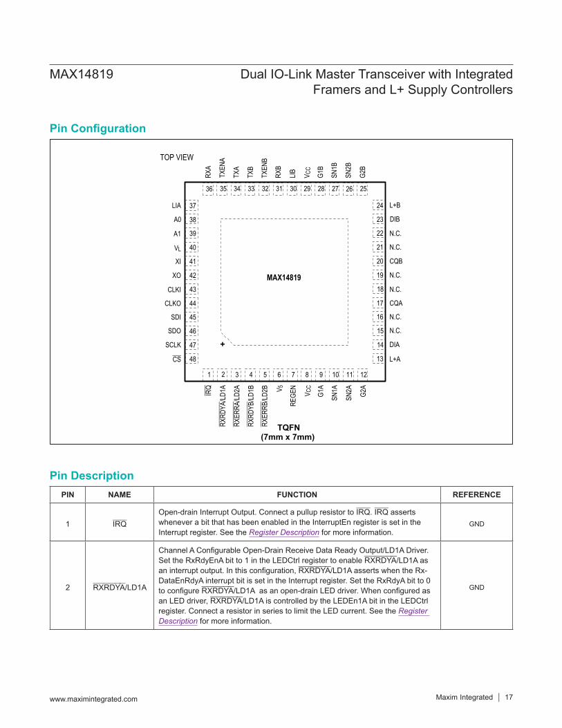
TOP VIEW
TQFN(7mm x 7mm)
13
14
15
16
17
18
19
20
21
22
23
24
L+A
+ DIA
N.C.
N.C.
CQA
N.C.
N.C.
CQB
N.C.
N.C.
DIB
L+B
48
47
46
45
44
43
42
41
40
39
38
37
1 2 3 4 5 6 7 8 9 10 11 12
CS
SCLK
SDO
SDI
CLKO
CLKI
XO
XI
VL
A1
A0
LIA
G2A
SN2A
SN1A
G1AV C
C
REG
ENV 5
RXER
RB/L
D2B
RXRD
YB/L
D1B
RXER
RA/L
D2A
RXRD
YA/L
D1AIRQ
36 35 34 33 32 31 30 29 28 27 26 25
G2B
SN2B
SN1B
G1B
V CC
LIB
RXB
TXEN
B
TXB
TXA
TXEN
A
RXA
MAX14819
MAX14819 Dual IO-Link Master Transceiver with Integrated Framers and L+ Supply Controllers
www.maximintegrated.com Maxim Integrated 17
Pin Description
Pin Configuration
PIN NAME FUNCTION REFERENCE
3 RXERRA/LD2A
ChannelAConfigurableOpen-DrainReceiveErrorOutput/LD2ADriver.Set the RxErrEnA bit in the LEDCtrl register to enable RXERRA/LD2A as an interruptoutput.Inthisconfiguration,RXERRA/LD2A asserts when the RxErrorA bit in the Interrupt register is set. Set the RxErrEnA bit to 0 to configureRXERRA/LD2Aasanopen-drainLEDdriver.Whenconfiguredasa LED driver, RXERRA/LD2A is controlled by the LEDEn2A bit in the LEDCtrl register. Connect a resistor in series to limit the LED current. See the Register Description for more information.
GND
4 RXRDYB/LD1B
ChannelBConfigurableOpen-DrainReceiveDataReadyOutput/LD1BDriver.Set the RxRdyEnB bit to 1 in the LEDCtrl register to enable RXRDYB/LD1B asaninterruptoutput.Inthisconfiguration,RXRDYB/LD1B asserts when the RxDataRdyB interrupt bit is set in the Interrupt register. Set the RxRdyEnB bit to 0toconfigureRXRDYB/LD1Basanopen-drainLEDdriver.Whenconfiguredasan LED driver, RXRDYB/LD1B is controlled by the LEDEn1B bit in the LEDCtrl register. Connect a resistor in series to limit the LED current. See the Register Description for more information.
GND
5 RXERRB/LD2B
ChannelBConfigurableOpen-DrainReceiveErrorOutput/LD2BDriver.Set the RxErrEnB bit in the LEDCtrl register to enable RXERRB/LD2B as an inter-ruptoutput.Inthisconfiguration,RXERRB/LD2B asserts when the RxErrorB bit intheInterruptregisterisset.SettheRxErrEnBbitto0toconfigureRXERRB/LD2Basanopen-drainLEDdriver.WhenconfiguredasanLEDdriver,RX-ERRB/LD2B is controlled by the LEDEn2B bit in the LEDCtrl register. Connect a resistor in series to limit the LED current. See the Register Description for more information.
GND
6 V5
5VSupplyInput/LinearRegulatorVoltageOutput.Connecta1μFbypasscapacitor as close as possible to the IC. Apply an external 5V supply to V5 if the internal 5V regulator is disabled (REGEN = GND). 5V must be present on V5 at all times for normal operation.
GND
7 REGEN5V Linear Regulator Enable Input. Leave REGEN unconnected to enable the internal 5V regulator. Connect REGEN to GND to disable the internal 5V regulator.
GND
8, 29 VCCVCC Supply Input. Bypass VCC to GND with a 1μFcapacitorascloseas possible to the device. GND
9 G1AChannel A Gate Drive Output 1. Connect G1A to the gate of the external PMOS1A to control the external reverse-current-blocking transistor of sensor supply A (L+A). Leave G1A unconnected if the external PMOS1A is not used.
SN1A
10 SN1AChannel A Sense Input 1/PMOS1A Source Connection. Connect a current-limiting resistor between SN1A and SN2A. Leave SN1A unconnected when the channel A supply controller is not used.
GND
11 SN2AChannel A Sense Input 2/PMOS2A Source Connection. Connect a current-limiting resistor between SN1A and SN2A. Connect SN2A to SN1A when current sensing is not used.
SN1A, GND
12 G2AChannel A Gate Drive Output 2. Connect G2A to the gate of the external PMOS2A for the channel A sensor supply (L+A). Leave G2A unconnected if the external PMOS2A is not used.
SNA1, GND
MAX14819 Dual IO-Link Master Transceiver with Integrated Framers and L+ Supply Controllers
www.maximintegrated.com Maxim Integrated 18
Pin Description (continued)
PIN NAME FUNCTION REFERENCE
13 L+A
Channel A L+ Sensor Supply Monitoring Input. Connect L+A to the drain of the externalPMOS2Acurrent-limitingtransistor.BypassL+AtoGNDwith0.47μF.Connecta100ΩresistorinserieswithL+A(seeTypical Operating Circuit). Connect L+A to GND or leave unconnected if not used.
GND
14 DIA ChannelAAuxiliaryDigitalInput.Connecta100ΩresistorinserieswithDIA(see Typical Operating Circuit). GND
15, 16, 18 ,19, 21, 22
N.C. No Connection. Not internally connected. —
17 CQA Channel A C/Q Transceiver Input/Output VCC, GND
20 CQB Channel B C/Q Transceiver Input/Output VCC, GND
23 DIBChannelBAuxiliaryDigitalInput.Connecta100ΩresistorinserieswithDIB(see Typical Operating Circuit). GND
24 L+B
Channel B L+ Sensor Supply Monitoring Input. Connect L+B to the drain of the external PMOS2B transistor to limit the load current sourced by the channel Bsourcesupply.BypassL+BtoGNDwith0.47μF.Connecta100Ωresistorinseries with L+B (see Typical Operating Circuit). Connect L+B to VCC or GND, or leave unconnected if not used.
GND
25 G2BChannel B Gate Drive Output 2. Connect G2B to the gate of the external PMOS2B for the channel B sensor supply (L+B). Leave G2B unconnected if the external PMOS2B is not used.
SN1B
26 SN2BChannel B Sense Input 2/PMOS2B Drain Connection. Connect a current-limiting resistor between SN1B and SN2B. Connect SN2B to SN1B or leave unconnected when current sensing is not used.
SN1B
27 SN1BChannel B Sense Input 1/PMOS1B Source Connection. Connect a current-lim-iting resistor between SN1B and SN2B. Leave SN1B unconnected when supply controller B is not used.
VCC
28 G1BChannel B Gate Drive Output 1. Connect G1B to the gate of the external PMOS1B to control the external reverse-current-blocking transistor of sensor supply B (L+B). Leave G1B unconnected if the external PMOS1B is not used.
SN1B
30 LIB Channel B Logic Output of the Digital Input (DIB). LIB is the logic inverse of the signal on DIB. VL, GND
31 RXB Channel B Logic Output of the CQB Receiver. RXB is the logic inverse of the signal on CQB (when InvCQB = 0). VL, GND
32 TXENB Channel B CQB Transmitter Output Enable. Drive TXENB high to enable the CQB driver. Drive TXENB low when using the internal UART. VL, GND
33 TXB Channel B CQB Transmitter Logic Input. CQB is the logic inverse of the signal on TXB (when InvCQB = 0 ). Drive TXB high when using the internal UART. VL, GND
34 TXA Channel A CQA Transmitter Logic Input. CQA is the logic inverse of the signal on TXA (when InvCQA = 0). Drive TXA high when using the internal UART. VL, GND
35 TXENAChannel A CQA Transmitter Output Enable. Drive TXENA high to enable the CQA driver. Drive TXENA low when using the internal UART. VL, GND
MAX14819 Dual IO-Link Master Transceiver with Integrated Framers and L+ Supply Controllers
www.maximintegrated.com Maxim Integrated 19
Pin Description (continued)

PIN NAME FUNCTION REFERENCE
36 RXA Channel A Logic Output of the CQA Receiver. RXA is the logic inverse of the signal on CQA (when InvCQA = 0). VL, GND
37 LIA Channel A Logic Output of the Digital Input (DIA). LIA is the logic inverse of the signal on DIA. VL, GND
38 A0SPI Chip Address Input A0. The MAX14819 is designed to allow up to 4 transceivers on the SPI at one time with a shared CS signal. Connect A1 and A0 high or low to set the individual IC SPI address. Do not leave A0 unconnected.
VL, GND
39 A1SPI Chip Address Input A1. The MAX14819 is designed to allow up to 4 transceivers on the SPI at one time with a shared CS signal. Connect A1 and A0 high or low to set the individual IC SPI address. Do not leave A1 unconnected.
VL, GND
40 VL
Logic Level Supply Input. VL sets the logic level of all logic inputs and outputs (TXEN_, TX_, RX_, LI_, and the SPI interface). Bypass VLtoGNDwitha0.1μFcapacitor as close as possible to the device.
GND
41 XICrystal Oscillator Input for Internal Framer Operation. Connect a crystal be-tween XI and XO to use crystal clocking. Leave XI unconnected if crystal clock-ing is not used.
V5, GND
42 XOCrystal Oscillator Output for Internal Framer Operation. Connect a crystal between XI and XO to use crystal clocking. Leave XO unconnected if crystal clocking is not used.
V5, GND
43 CLKILogic Clock Input for Internal Framer Operation. When not using a crystal for framer operation, connect a 3.686MHz clock signal to CLKI. Connect CLKI to GND when not used.
V5, GND
44 CLKO
Logic Clock Output for Internal Framer Operation. CLKO outputs a 3.686MHz clock signal when enabled (ClkOEn = 1). When using multiple MAX14819 ICs on a board, these can be clocked with a single crystal by connecting the CLKO output of one device to the CLKI inputs of the other(s).
V5, GND
45 SDI SPI Data Input. Connect SDI to the MOSI output of the microcontroller. V5, GND
46 SDO SPI Data Output. Connect SDO to the MISO input of the microcontroller. V5, GND
47 SCLK SPI Clock Input. Connect SCLK to the CLK output of the microcontroller. V5, GND
48 CSSPI Chip-Select Input. The SPI cycle begins when CS is driven low and ends when CS is driven high. Up to 4 MAX14819 ICs can share a single SPI bus and CS input using the A1 and A0 address inputs.
V5, GND
EP ― Exposed Pad. Connect to GND. GND
MAX14819 Dual IO-Link Master Transceiver with Integrated Framers and L+ Supply Controllers
www.maximintegrated.com Maxim Integrated 20
Pin Description (continued)
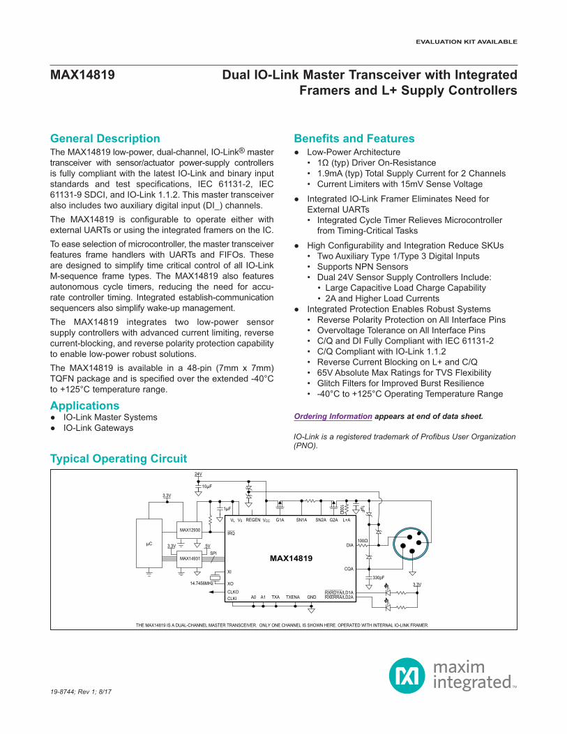
Detailed DescriptionThe MAX14819 low-power dual-channel industrial IO-Link master transceiver is fully compliant with the latest SDCI/ IO-Link standards and test specifications. The MAX14819 features two integrated framers but can alternatively oper-ate with external UARTs.The MAX14819 features a high-speed SPI interface for system-side data and control interfacing. Integrated IO-Link message frame handlers and FIFOs simplify time critical control and cycle time management of all IO-Link M-sequence communication, easing data link layer con-trol. Autonomous cycle timers also reduce the need for accurate controller timing. Integrated establish-communi-cation sequencers simplify wake-up management. The MAX14819 further includes two sensor supply con-trollers (L+A, L+B) with current limiting and reverse cur-rent blocking. The current limit is set with external sense resistors.
POWER Power-UpThe CQ_ driver outputs are high impedance when the VCC supply, V5, and VL voltages are below their respec-tive undervoltage thresholds during power-up.The drivers are automatically disabled when the VCC voltage falls below the 9V (typ) UVLO threshold. The SPI interface remains active while V5 and VL are present.
VCC Low Voltage and Undervoltage DetectionThe MAX14819 monitors the VCC supply for low-voltage and undervoltage conditions. Low-voltage warnings are reported in the Status register and can be configured to generate an interrupt on the IRQ output.When VCC falls below the 18V (max) low-voltage warn-ing threshold, the VCCWarn and VCCWarnCOR bits in the Status register are set. If VCCWarnCOR in the Clock register is set, a StatusInt interrupt is generated and IRQ asserts.When VCC falls below the 9V (max) undervoltage-lockout (UVLO) threshold, the VCCUV and VCCUVCOR bits in the Status register are set. A StatusInt interrupt is generated and IRQ asserts.
5V Linear RegulatorThe MAX14819 includes an integrated regulator to gener-ate 5V (V5). To enable the internal regulator, leave REGEN unconnectedandconnecta1μFbypasscapacitorbetweenV5 and ground as close as possible to the device. The internal V5 regulator is capable of driving external loads up to 20mA. When the internal 5V linear regulator is not used, V5 is the supply input for the internal analog and digital functions and must be supplied externally. Connect REGEN to ground to disable the internal regulator when applying an external 5V to V5. Ensure that V5 is present for normal operation.An internal undervoltage lockout comparator detects when the V5 voltage falls below the 3.5V (typ) V5_UVLO threshold. When the V5 voltage drops below this level, the device is under reset: SPI registers are reset to their power-up state, the CQ_ outputs and L+_ supplies are disabled, internal pullups/pulldowns are turned off, the CQ_ and DI_ receivers are disabled, and the LED outputs are high impedance. When the V5 voltage rises above the UVLO threshold, the MAX14819 restarts in the default power-on configuration.The internal V5 regulator output is not protected against short circuits.
Logic Supply (VL) The VL input is the logic-level supply for all the digital I/Os. Apply a voltage between 1.62V and 5.5V to VL for normal operation. Internal UVLO circuitry monitors the VL supply. If VL falls below the 0.7V (typ) VL UVLO threshold, all the digital I/Os referred to VL are ignored and either set to high impedance or are low.
L+ Sensor Supply ControllersThe MAX14819 includes one sensor/actuator supply controller for each IO-Link channel, L+A and L+B. Each sensor supply is configurable through the SPI interface and must be enabled by setting the L+En_ bit in the L+Cnfg_ register. Using external pMOS transistors, these controllers provide active current limiting, reverse current blocking, and undervoltage detection. The 24V VCC field supply input is tolerant to reverse voltage and the L+A/L+B output is negative voltage capable down to VCC - 60V.
MAX14819 Dual IO-Link Master Transceiver with Integrated Framers and L+ Supply Controllers
www.maximintegrated.com Maxim Integrated 21
Setting the L+_ Current LimitThe L+_ sensor supply current is limited by placing a sense resistor between the SN1_ and SN2_ current-sense inputs. When the voltage across the resistor reaches the VCL_T (15mV, typ) threshold, the gate of the pMOS (G2_) is actively controlled to limit the load current such that:
ILIM = VCL_T/RSENSEIf the L+_ voltage is pulled below ground (< -3V), the current limit is reduced to about 10% of normal value to reduce the power dissipated in the external pMOS.
L+_ Blanking Time and Autoretry FunctionalityThe L+_ controllers have programmable variables (set in the L+Cnfg_ registers) that allow the system to optimize turn-on and charging large loads while protecting the pMOS FETs in cases of shorts and challenging load condi-tions. If the load current is in current limiting for a period exceed-ing the set blanking time, the gate drive (G2_) is turned off. The sensor supply is then either turned off until the controller reenables it, or is turned on again following the autoretry delay.To further reduce the power dissipated in the pMOS tran-sistors during turn-on of loads that require large inrush currents (e.g., capacitive loads), the current limiter includes a dynamic blanking time mode that reduces the blanking time when the voltage across the pMOS is high, limiting the pulse energy during the initial turn-on phase. Dynamic blanking time mode is operational when the L+_ output voltage is below 18V and must be enabled by setting the L+DynBl_ bit in the L+Cnfg_ register. The MAX14819 current-limit circuitry also includes the option to double the L+_ load current when the L+_ supply voltage is above 18V. This functionality is enabled by setting the L+CL2x_ bit in the L+Cnfg_ register.
Bypassing the L+_ Sensor SuppliesWhen the internal L+_ supply controllers are not used, leave all the associated pins (G1_, G2_, SN1_, SN2_, L+_) unconnected. L+_ can also be connected to GND.
CQ_ TransceiversThe CQA and CQB drivers are independently con-figurable as push-pull, NPN, or PNP mode outputs in the SPI registers. Set the bits in the CQCfgA and CQCfgB registers to configure the drivers, enable or disable internal pullup and pulldown current sources on the CQ_ I/Os, and to set the digital input thresholds. The CQ_ drivers can also be enabled/disabled in these registers.
CQ_ Current Limit and Thermal ProtectionThe MAX14819 features a selectable current limit for both CQ_ drivers ranging from 100mA to 500mA. Set the CL[1:0] bits in the DrvrCurrLim register to select the current limit for the drivers. The CQ_ drivers are independently thermally protected. If one output driver temperature rises above the 160°C threshold, that output is disabled until the temperature drops below 145°C.
CQ_ Driver Fault DetectionThe MAX14819 senses a fault condition on the CQ_ driver when an overcurrent event exists for longer than the blanking time. Both the current limit and blanking time can be configured in the DrvrCurrLim register.When a short-circuit fault occurs on CQ_, the CQFault_ and CQFaultCOR_ bits in the ChanStat_ register are set and can trigger an interrupt.When an overcurrent event occurs on CQ_, the driver can either be set to continue supplying the selected current until the device enters thermal shutdown (autoretry is dis-abled), or to enter autoretry mode. In autoretry mode, the driver is automatically disabled after the current blanking time and is then reenabled.
CQ_ Reverse-Polarity ProtectionThe CQ_ outputs are protected against reverse polarity vs. ground. If CQ_ is connected to a negative voltage, the driver is automatically disabled and CQ_ is set to high impedance.When CQ_ is shorted to a voltage above VCC, the driver is automatically disabled and the output is set to high impedance.During a reverse condition, positive or negative, when no fault is detected on CQ_ but the internal diode begins to overheat, the L+_ supply is immediately disabled (turning off the external transistors) to protect the device.Reverse conditions do not generate a fault or interrupt.
CQ_ Current Sources/SinksThe MAX14819 features programmable internal 2.5mA/5.8mA pullup/pulldown current sources on the CQ_ receivers. Select the pullup/pulldown current for each CQ_ I/O by setting the SinkSel_[1:0] bits in the CQCfg_ register. The internal pullup/pulldown currents are automatically disabled when the CQ_ output is driven (i.e., push-pull not in high-impedance state, NPN mode is set low, or NPN mode is set high).
MAX14819 Dual IO-Link Master Transceiver with Integrated Framers and L+ Supply Controllers
www.maximintegrated.com Maxim Integrated 22

CQ_ Receiver Output (RXA/RXB)RX_ is the output of the CQ_ receiver. By default, the RX_ output is the inverse logic of the CQ_ input. Setting the InvCQ_ bit in the MsgCtrl_ register inverts CQ_ so that the RX_ output is the same logic of the CQ_ input. RX_ cannot be disabled/three-stated.CQ_ Receiver ThresholdThe CQ_ receiver thresholds are compliant with the IO-Link standard by default. The receiver thresholds are also configurable to be compatible with the IEC 61131-2 type 1 and type 2/3 digital inputs. Set the IEC3Th_ bit in the CQCfg_ register to select the input thresholds for each receiver.CQ_ Receiver DeglitchThe CQ_ receivers feature a selectable glitch filter for improved noise immunity. Enable/disable this filter by setting the CQFilterEn_ bit in the CQCfg_ register. Transients longer than 1.3µs (typ) are ignored when the glitch filter is enabled.DI_ ReceiverThe MAX14819 includes two auxiliary digital inputs: DIA and DIB. These inputs are protected against reverse polarity (referred to VCC and/or GND). DI_ inputs are configurable in the IOStCfg_ registers. Set the DiCSource__ bit to enable the internal 2.4mA source on the DI_ input. Set the DiCSink_ bit to enable the 2.4mA sink on the input. Each DI_ input also features a selectable glitch filter for improved noise immunity. Transients longer than 1.3µs (typ) are ignored when the glitch filter is enabled. Set the DiFilterEn_ bit to enable or disable this filter. When the glitch filter is enabled, signal pulses less than 1μs areignored on the DI_ input.The DI_ receiver thresholds are configurable to be compatible with the IEC 61131-2 type 1, and type 2/3 digital inputs. Set the DiEC3Th_ bit in the IOStCfg_ register to select the input thresholds for each receiver.
SPI InterfaceThe MAX14819 is connected to a microcontroller or SPI-host through an SPI-compatible serial interface. The interface has three inputs: clock (SCLK), chip select (CS), and data in (SDI), and one output, data out (SDO). SDO is high impedance when CS is high, allowing multiple SPI slave devices to share a common bus. The SPI is not daisy-chainable. The maximum SPI clock rate is 20MHz when VL > 2.5V. The SPI interface logic complies with SPI clock polarity (CPOL = 0) and clock phase (CPHA = 0). The SPI
interface supports both byte-by-byte cycle and burst mode read and write.In both read and write cycles, the SDO signals the IRQ status, as well as the receive-data-ready and receive-data-error for both receivers A and B (Figure 6 and Figure 7).The SPI interface is not available when the VL voltage is below the 0.7V (typ) VL UVLO threshold or when 5V is not present on V5. The SPI registers are reset to their default state when the V5 voltage falls below the 3.5V V5 UVLO threshold.SPI Chip Address (A1, A0)The MAX14819 is designed to allow up to four master transceivers on a single bus with a single/shared CS. This is accomplished using SPI-addressable devices with logic address inputs A1 and A0. See Table 1. Do not leave the A1 or A0 address input unconnected. Each chip on the SPI bus should be assigned an individual chip address. The MAX14819 monitors the SPI address in each read/write cycle and responds when the SPI address matches the pin-programmed address for that IC. SPI trigger commands are global and are not filtered by the chip address. All MAX14819 devices connected to the SPI bus will react to a received trigger command.SPI In-Band IRQ InterruptThe addressed MAX14819 sends out an IRQ bit on SDO in every SPI cycle (both in single cycle as well as burst mode), beginning on the third SPI clock. This bit is equivalent to the IRQ interrupt output pin logic, but inverted (active high). The IRQ bit is set when the IRQ pin is asserted. Similarly, when the IRQ output is high imped-ance, the IRQ bit is 0. See Figure 6 and Figure 7. The IRQ bit cannot be masked.
SPI In-Band Device-Message-Ready SignalingIn addition to sending IRQ status, the addressed MAX14819 can be enabled to also send out 2 bits per channel in every SPI cycle that provide information, whether the IO-Link device answer message was received correctly (RRDY_) or in error (RERR_) (Figure 6 and Figure 7). Set the RMessgRdy_ bits in the MesgCrtl_ register to enable this functionality.
Table 1. SPI MAX14819 Chip Address SelectA1 A0 DEVICE ADDRESS
LOW LOW 00
LOW HIGH 01
HIGH LOW 10
HIGH HIGH 11
MAX14819 Dual IO-Link Master Transceiver with Integrated Framers and L+ Supply Controllers
www.maximintegrated.com Maxim Integrated 23
Figure 6. SPI Byte-by-Byte Write Cycle
Figure 7. SPI Byte-by-Byte Read Cycle
CS
SCLK
SDI
SDO
W A1 A0 R4 R3 R2 R1 R0 D7 D6 D5 D4 D3 D2 D1 D0
IRQ RERRB RRDYB RERRA RRDYA A1 A0 R4 R3 R2 R1 R00
A_ = Chip AddressR_ = Register AddressD_ = Data Bit
RRDY_ = Receive Data Ready InterruptRERR_ = Receive Data Error Interrupt = Clock Edge upon which SDI data is latched = Clock Edge upon which SDO is generated
IRQ = IRQ Bit
CS
SCLK
SDI
SDO
R A1 A0 R4 R3 R2 R1 R0
IRQ RERRB RRDYB RERRA RRDYA D6 D5 D4 D3 D2 D1 D0D7
A_ = Chip AddressR_ = Register AddressD_ = Data Bit
RRDY_ = Receive Data Ready InterruptRERR_ = Receive Data Error Interrupt = Clock Edge upon which SDI data is latched = Clock Edge upon which SDO is generated
IRQ = IRQ Bit
MAX14819 Dual IO-Link Master Transceiver with Integrated Framers and L+ Supply Controllers
www.maximintegrated.com Maxim Integrated 24

The RRDY_ bits are equivalent to the DtaRdy_ hardware outputs. Similarly, the RERR_ bits are the equivalent to the RxErr_ hardware outputs. The SDO bit logic is the inverse of the pin logic: when the pin output is low, the associated bit is set to 1, and when the pin output is high, the associated bit is 0. The RRDY_ bits and the RXRDY_ pins are cleared auto-matically when the device message is read out of the RxFIFO_.
SPI Burst AccessBurst access allows SPI reading/writing of two or more bytes in a single SPI cycle. The chip-select input (CS) must be held low during the entire burst write/read cycle.
The SPI clock must continue clocking throughout the burst access cycle. Only the initial register address is sent, followed by multiple bytes of data. The burst cycle ends when the SPI master pulls CS high. See Figure 8.When performing a burst read or write of/to the TxRxData_ registers, the register address remains the same, allowing fast loading of a master message into the TxFIFO_ and reading of the device message out of the RxFIFO_. When burst reading or writing of registers having a higher address than the TxRxData_ registers, the register address is automatically incremented, allowing reading and writing of a consecutive register block by only defin-ing the initial register address in the SPI command byte.
Figure 8. SPI Burst Read/Write and Byte-by-Byte Read/Write Overview
SPI BYTE-BY-BYTE WRITE
COMND Data1 COMND Data2 COMND Data3
IC AND REGISTER ADDRESS
CS
SDI
SPI BYTE-BY-BYTE READ
COMND COMND COMND
CS
SDI
Data1 Data2 Data3SDO
CS
SPI BURST WRITE
SDI COMND Data1 Data2 Data3 Data(N-1) DataN
IC AND REGISTER ADDRESS
CS
SPI BURST READ
SDI COMND
SDO Data1 Data2 Data3 Data(N-1) DataN
SDO Data0 COMND Data1 Data2 Data(N-2) Data(N-1)
Data0
SDO Data0 Data0 Data0
Data0 Data0 Data0
COMND COMND COMND
MAX14819 Dual IO-Link Master Transceiver with Integrated Framers and L+ Supply Controllers
www.maximintegrated.com Maxim Integrated 25

Wake-Up Pulse GenerationThe MAX14819 can automatically generate a wake-up pulse to initiate IO-Link communication. Set the CQ_ driver into receive mode (TXEN = low or TxEn_ = 0), and drive TX_ low or set the Tx_ bit to 0 before the wake-up sequence begins. Set the WuPuls_ bit to begin the wake-up sequence. When the WuPuls_ bit is set, the MAX14819 samples the CQ_ voltage level and then automatically enables the CQ_ driver. A 500mA current pulse of opposite polarity is applied to the CQ_ line for 80μs (typ). During the wake-up pulse, the CQ_ currentlimit is temporarily set above 500mA internally, although the CL_ register bits are not changed. The driver remains enabled, the line returns to the original polarity, and after a 100μs(typ)delaytheMAX14819CQ_driverissettohighimpedance (Figure 9). The WuPuls_ bit is automatically cleared after the tON_WU delay.
Microcontroller Data InterfaceThe MAX14819 offers two interface options for IO-Link communication. When used as a transceiver, external UARTs are required in the microcontroller and these are interfaced to the TX_, RX_ and TXEN_ pins. If the IO-Link framers in the MAX14819 are used, then the SPI is used for interfacing to the microcontroller.
Framer CommunicationThe MAX14819 includes two independent IO-Link framers with UARTs, one for each CQ_ channel. Each framer operates in a Master-message (TX)/Device-message (RX) doublet, verifying communication timing and data transmitted/received. After a channel has complet-ed transmission of a master message, the framer is automatically switched into receive mode. When the expected number of bytes has been received, the framer automatically exits from receive mode and any further received data is ignored.
UART FramingThe UART frame is made up of one start bit, 8 data bits with 1 even parity bit and 1 STOP bit. When transmitting, the idle time between the STOP bit and the following START bit is less than 1 bit interval.
Frame Handler FIFOs (TxRxFIFOA/TxRxFIFOB)Each IO-Link channel on the MAX14819 (CQA and CQB) has a transmit and receive FIFO for buffering the IO-Link M-sequence messages that are sent and received. These FIFOs have a depth (66 bytes) to buffer the largest M-sequence, Type 2.V, in addition to the two length bytes.
Transmit/Receive FIFO Data StructureTo ensure proper communication, the message from the SPI master to the TxFIFO_ must follow the sequence shown in Figure 10.
Figure 9. Wake-Up Timing
Figure 10. Transmit SPI Data Write Sequence
WuPuls_ Bit 0 1
CQ_ VOLTAGE
WAKE-UP PULSEtWU
tSU_WU tON_WU
SDI RxBytes TxBytesTxData-1
(MC)TxData-2
(CKT)TxData-n
MAX14819 Dual IO-Link Master Transceiver with Integrated Framers and L+ Supply Controllers
www.maximintegrated.com Maxim Integrated 26

RxBytes is the number of octets the IO-Link device is expected to reply with after it receives this master message. TxBytes is the number of bytes that the mas-ter will send to the device in this message (the master message length).The IO-Link device answers with the device message, which is stored in the RxFIFO_. When the RxFIFO_ on the MAX14819 is read, the data is formatted as shown in Figure 11. RxBytesAct is the actual number of bytes received from the device and available for readout from the RxFIFO_. This may differ from the expected number of receive bytes (RxBytes).
Loading the Transmit FIFO (TxFIFO_)The master message is loaded into the transmit FIFO (TxFIFO_) through the SPI interface. The SPI master needs to send three pieces of information to the TxRxData_ register for a complete master message (Figure 12): 1) A byte describing the expected number of bytes of
the IO-Link device reply message. This is RxBytes. 2) A byte describing the number of bytes in the master
message (the length that will be transmitted). This is TxBytes.
3) The data for the master message.The TxBytes byte signals the number of octets in the master message and the RxBytes indicates the num-
ber of octets expected from the device in the response message. Set the TSizeEn_ bit in the MsgCtrl_ register to compare the TxBytes information to the number of octets loaded in the TxFIFO_ and verify that the full message has been received by the SPI master. The TSizeEn_ functionality can be used either for byte-by-byte FIFO loading or for burst loading. When a size error is detected, a TSizeErr_ interrupt is generated. The TxFIFO_ can be written to using byte-by-byte write or a burst write. When loading the TxFIFO_ with byte-by-byte writing, the CQ_ transmission can be started before the complete master message is loaded into the TxFIFO_ (transmission and TxFIFO_ loading can be done in paral-lel). In this case, the SPI controller must set the InsChks bit in the MsgCtrl_ register to 0 and include the 6-bit checksum in the master message CKT octet, since the MAX14819 cannot calculate it. The MAX14819 can only generate a TChkSmEr_ interrupt after the whole message is loaded into the TxFIFO_; if transmission is started before the full message was loaded, it is possible that the IO-Link device will receive a message with a checksum in error. When transmission starts after the TxFIFO_ is com-pletely loaded, the MAX14819 can calculate and insert the checksum (when InsChk_= 1) into the CKT octet. Alternatively, the SPI master can insert the checksum in the master message and the MAX14819 will verify the data (SPIChks_ = 1). If a checksum error is detected, a
Figure 11. Receive SPI Data Read Sequence
Figure 12. Message Timing
SDO RxBytesAct RxByte-1 RxByte-2RxBytes-m
(CKS)
UART FRAME
UART FRAME
UART FRAME
UART FRAME
UART FRAME
UART FRAME
MASTER MESSAGE
DEVICE RESPONSE
t1 t1
t2 t2tA
tM-sequence
MAX14819 Dual IO-Link Master Transceiver with Integrated Framers and L+ Supply Controllers
www.maximintegrated.com Maxim Integrated 27
TChksmEr_ interrupt is generated and the MAX14819 does one of two things, depending on the state of the TxErDestroy_ bit in the MsgCtrl_ register:
If TxErDestroy = 1: The MAX14819 will not send the message, so the SPI master must reload the message into the TxFIFO_ in time for the cycle time.
If TxErDestroy = 0: The MAX14819 sends the mes-sage with the error.
Initiating TransmissionTransmission on CQ_ is initiated either by setting the CQSend_ bit in the CQCtrl_ register or by using a trigger command (see the TrigAssgn_ register for more informa-tion). Transmission can also be initiated cyclically when the internal cycle time is enabled (CyclTmrEn_=1). When SPI burst write mode is used, transmission must be initiated after the TxFIFO_ is loaded or the MAX14819 generates a cycle error interrupt (TCycleErr_ = 1). When using byte-by-byte SPI write mode, transmission can be initiated before the complete master message is loaded. When using this mode, ensure that the TxFIFO_ always has at least 1 data byte stored in it to avoid any idle time or errors. The TxFIFO_ transmission is halted and the CQ_ transceiver is configured to receive mode as soon as the TxFIFO_ is empty. During transmission, the CQ_ transmitter is set to push-pull mode. CQ_ is restored to the previous state when transmission is complete.
Transmit Loopback CheckThe internal framers automatically verify transmitted data through a loopback check. During transmission, the signal at CQ_ is automatically routed to the receiver and the message sent is checked against the data sent out. If inconsistencies are detected (e.g., when a CQ_ line is shorted), the TransmErr_ bit is set and a TxError_ interrupt can be generated.
Receiving the Device MessageWhen the MAX14819 completes transmission of the master message to the IO-Link device, the CQ_ transmitter issettoreceivemodewithin3μs(typ)andthemasterwaitsfor the device reply message. The MAX14819 waits for 9 to 24 bit times (set by the DDelay_ bits in the DeviceDly_ register) for a valid START from the device.From the RxBytes data in the master message, the MAX14819 already knows the number of bytes expect-ed to be returned from the device. If the number of bytes received is not the expected number, a RSizeErr_ interrupt is generated. The receiver stops reception when the number of received bytes equals the value in RxBytes
and any further data sent from the device is ignored. Reception is also terminated when less bytes are received than expected. The MAX14819 determines this to be the case when no START bit occurs within 2 to 5 bit times (as set in the BDelay_ bits in the DeviceDly_ register) after the last character’s STOP bit. When the device message is received success-fully (without any errors), an RxDataRdy_ interrupt is signaled to the host SPI controller by asserting the IRQ pin (if (RDaRdyIntEn = 1) and/or by asserting the RXRDY_/LD1_ pin when the received data (device message) is ready for readout from the RxFIFO_. The host controller can read out the message from the RxFIFO_ in byte-by-byte mode or in a single-burst SPI cycle. The IRQ and/or RXRDY/LD1_ interrupts are automatically cleared when the first byte of the message is read out of the RxFIFO_, or alternatively, by reading the Interrupt register. If the device message is not received successfully (i.e., received with an error), an RxError_ interrupt is signaled to the host controller by asserting the IRQ pin (if RxErrIntEn_ = 1) and/or by asserting the RXERR_/LD2_ pin. Detected errors in the received data can include checksum, parity, UART framing, or size deviations. The RxError_ interrupt is cleared only when the Interrupt register is read.
Monitoring Message TimingThe IO-Link standard requires that the device reply message must be fully received within a time of tM-sequence after the start of the communication cycle:
tM-sequence = (m+n) x 11 x TBIT + tA + (m-1) x t1 + (n-1) x t2
where m is the number of octets in the master message, n is the number of octets in the device message, TBIT is the bit time at the present COM data rate, tA (max) is 10 bits, t1 is a maximum of 1 bit, and t2 is a maximum of 3 bits (Figure 12). The MAX14819 can be set to generate an error if the device message is not completely received in the expected tM-sequence window. Set the RspnsTmrEn_ bit in the DeviceDly_ register to enable the internal message timing monitor.While the IO-Link standard specifies tM-sequence as the longest allowable delay, actual IO-Link devices may exhibit longer delays (e.g., a longer delay can occur when tA exceeds more than 10 x TBIT). The MAX14819 can be set to allow for these tolerances. Set the BDelay_[1:0] and DDelay_[3:0] bits in the DeviceDly_ register to add additional delay. For IO-Link compliance, set BDelay_[1:0] = 01b and DDelay_[3:0] = 0001b. If a device message is
MAX14819 Dual IO-Link Master Transceiver with Integrated Framers and L+ Supply Controllers
www.maximintegrated.com Maxim Integrated 28

not received or not completely received in this time, the RxErr_ interrupt is signaled.
Checksum Calculation and CheckingThe MAX14819 can perform standard IO-Link 6-bit check-sum calculation and checksum verification. This can be used to generate the master message checksum auto-matically, to check the integrity of the master message from the SPI master to the TxFIFO_, and to check the received device message.Set the InsChks_ bit in the MsgCtrl_ register to enable master-message checksum generation. When enabled, the checksum bits from the SPI master are ignored and the MAX14819 inserts the calculated checksum bits into the CKT octet before transmission. The master message must be completely loaded into the TxFIFO_ before transmission for the MAX14819 to insert the calculated checksum into the message.Set the SPIChks_ bit in the MsgCtrl_ register to enable the MAX14819 to verify the current checksum in the CKT octet in the TxFIFO_ with the calculated master-message checksum. If a difference is detected, a TChksmEr_ interrupt is generated. When the TxErDestroy_ bit in the MsgCtrl_ register is set, the master message is deleted in the TxFIFO_ and is not sent to the IO-Link device. In SPI byte-by-byte write mode, the master message is deleted only if the complete master message has been loaded into the TxFIFO before transmission is initiated.
Establish-Communication SequencerThe MAX14819 features an integrated IO-Link establish-communication sequencer to autonomously perform the IO-Link establish-communication wake-up sequence. The wake-up sequence is the prerequisite for placing the device in IO-Link pre-operate and operate modes. Set the EstCom_ bit in the CQCtrl_ register to begin the autono-mous establish-communication sequencer. When the EstCom_ bit is set, the MAX14819 generates an 80μs(typ)wake-uppulseontheCQ_lineandthenautono-mously determines the COM rate and minimum cycle time of the attached IO-Link device. No further direction is required from the SPI controller at this time. Once the sequence is successfully completed, the COM rate of the IO-Link device is stored in the ComRt_ bits of the CQCtrl_ register. Similarly , the minimum cycle time of the device is stored in the CyclTmr_ register.If the first establish-communication sequence fails, the MAX14819 repeats the sequence again after a 30ms delay. If the sequence fails again, a third attempt is made. If the third attempt fails, the MAX14819 stops attempt-ing to establish communication with the device and a
WURQInt interrupt is generated, the EstCom_ bit is reset, and the CQ_ driver is returned to SIO mode after 300ms (max). A new establish-communication sequence can then be initiated by the SPI controller by setting the EstCOM_ bit.
Transmitter SynchronizationThe start of master-message transmission can be synchronized on multiple IO-Link ports, so that ports that operate with the same cycle time receive the master message simultaneously. Triggering allows synchronization of master ports on one or many MAX14819 devices being driven by a common SPI. Assign the same trigger value to ports that will be synchronized in the TrigAssgn_ registers and enable synchronization by setting the TrigEn_ bit. Write an SPI trigger value to the Trigger register to initiate immediate transmission of the data in the TxFIFOs assigned to that trigger value. Trigger is a global SPI command and is not filtered by the SPI address bits, making it possible to synchronize the transmitters of multiple MAX14819 devices on a single SPI bus with a single trigger command.Trigger functionality can also be used with the internal cycle timer. When configured for this, the cycle timer is immediately started when its trigger value is received.
Trigger Delay and Synchronization AccuracyThe delay between the time when the MAX14819 receives a trigger command and the time when the associated CQ_ transmitter starts transmission is made up of a fixed and a variable component, which depends on the UART data rate. The time (tTRIG) between the last rising edge of the serial clock (SCLK) and the beginning of the CQ_ START bit is:
• COM3:0.813μs≤tTRIG≤1.085μs• COM2:4.881μs≤tTRIG≤6.508μs• COM1:39.060μs≤tTRIG≤52.080μs
The reference point is the time when the trigger command is received by the MAX14819. This occurs on the final (i.e., the 16th) SPI clock’s low-to-high transition (Figure 13).When synchronizing multiple CQ transmitters, the trigger delay skew of the CQ_ transmitter outputs is based on the triggering delays of each transmitter (see Figure 14). This skew has a baud-rate-dependent component, similar to the trigger accuracy equation for a single transmitter output. Calculate the CQ_ transmitter output skew using the fol-lowing equation:
tTRIG_SKEW(max)≤(4BTS - 3BTF) / 16Where BT is the bit time of the CQ_ data (= 1/COM rate), BTS is the bit time of the lower bit rate (e.g., COM1), and BTF is the bit time of the faster bit rate.
MAX14819 Dual IO-Link Master Transceiver with Integrated Framers and L+ Supply Controllers
www.maximintegrated.com Maxim Integrated 29
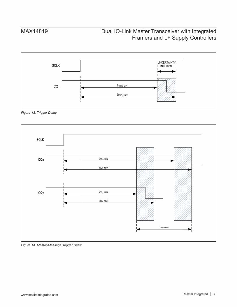
Figure 13. Trigger Delay
Figure 14. Master-Message Trigger Skew
tTRIG_MIN
tTRIG_MAX
UNCERTAINTY INTERVALSCLK
CQ_
tCQn_MIN
tCQn_MAX
tTRIGSKEW
SCLK
CQn
tCQy_MIN
tCQy_MAX
CQy
MAX14819 Dual IO-Link Master Transceiver with Integrated Framers and L+ Supply Controllers
www.maximintegrated.com Maxim Integrated 30

When synchronizing ports that use the internal cycle timers, the skew between channels will be larger, ranging from0μsto(BT/16+101μs).
Cycle TimerThe MAX14819 features two cycle timers (one for each CQ_ transceiver) that autonomously send the master message from the TxFIFO_ at predefined time intervals. The bits in the CyclTmr_ register set the time interval. The smallestcycletimesupportedbythecycletimeris400μs.The minimum cycle time of the attached IO-Link device is automatically determined during the establish-commu-nication cycle and is stored in the CyclTmr_ register. The SPI master can overwrite these values with the cycle time required by the application.To start the cycle timer sending the first master message, either send its trigger value or set the CQSend_ bit in the CQCtrl_ register.At the start of each cycle, the CQ_ transmitter is enabled and the master message sent. The CQ_ transceiver is then automatically switched to receive mode (within 1 bit interval) and the MAX14819 waits for the IO-Link device response message. When the complete device message is received, an RxDataRdy_ interrupt is triggered.When the data ready interrupt is triggered, the SPI master must read out the device message from the RxFIFO. The following master message must then be written into the TxFIFO, if the TxKeepMsg_ bit is not set. A TxError_ interrupt is generated due to TCycleErr_ if the SPI master does not load the next master message in time.
ClockingIf external UARTs of a microcontroller are used, external clock sources are not required since the MAX14819 has adequate internal clocking. If the internal framers are used instead of external UARTs, external clocking from a crystal or clock source is required to achieve the timing accuracy required for IO-Link communication (Figure 15). Set the ClkDiv[1:0] bits in the Clock register to select the
input (crystal or clock) frequency: 3.686MHz, 7.372MHz, or 14.745MHz. Set the ComRt_[1:0] bits in the CQCtrl_ register to determine the COM rate on the CQ_ interface. Set the ExtClockEn bit in the Clock register to enable clocking from an external clock source on the CLKI input. Set the XtalEn bit and clear the ExtClkEn bit if a crystal is used for clocking.Set the ClkOEn bit in the Clock register to enable the clock signal on the CLKO output. When ClkOEn is set, a 3.6864MHz clock output is routed to CLKO, allowing multiple MAX14819 transceivers to operate from a single crystal oscillator.An internal oscillator is used for basic functionality when both the crystal oscillator and the external clock are disabled. SPI read/write functionality is also available when no valid external clock source is present.
LED ControlThe MAX14819 features four logic outputs that can be used for driving LEDs: LD1A, LD1B, LD2A, LD2B. LED functionality is controlled by setting the bits in the LEDCtrl register.
Thermal ProtectionThermal Shutdown The CQ_ drivers are automatically disabled when the driver temperature exceeds the +160°C (typ) thermal-shutdown threshold. Drivers are automatically switched on when the driver temperature falls below the thermal-shutdown threshold plus hysteresis. The MAX14819 generates a thermal-shutdown interrupt (ThShdnCOR = 1) in the Status register when thermal shutdown occurs.
Overtemperature WarningWhen the junction temperature exceeds the +135°C (typ) overtemperature-warning threshold, the TempWarn bit in the Status register is set.The TempWarn bit is cleared when the die temperature falls to +120°C (typ).
Figure 15. Clock Generation
CRYSTAL OSCILLATOR
DIVIDER
BAUD-RATE GENERATOR
A
BAUD-RATE GENERATOR
B
XO
XI
CLKI
CLKO
XtalEn ExtClockClkDiv1 ClkDiv0 ComRtA1 ComRtA0 ComRtB1 ComRtB0
UART A
UART B
MAX14819 Dual IO-Link Master Transceiver with Integrated Framers and L+ Supply Controllers
www.maximintegrated.com Maxim Integrated 31

Register Map
*Bit is unused.
REGISTER NAME
CH/ GLOBAL
REG ADDRESS BIT 7 BIT 6 BIT 5 BIT 4 BIT 3 BIT 2 BIT 1 BIT 0
TxRxDataA A 0x00 DataA7 DataA6 DataA5 DataA4 DataA3 DataA2 DataA1 DataA0
TxRxDataB B 0x01 DataB7 DataB6 DataB5 DataB4 DataB3 DataB2 DataB1 DataB0
Interrupt G 0x02 StatusInt WURQInt TxErrorB TxErrorA RxErrorB RxErrorA RxDataRdyB RxDataRdyA
InterruptEn B 0x03 StatusIntEn WURQIntEn TxErrIntEnB TxErrIntEnA RxErrIntEnB RxErrIntEnA RDaRdyIntEnB RxDaRdyIntEnA
RxFIFOLvlA A 0x04 FifoLvlA7 FifoLvlA6 FifoLvlA5 FifoLvlA4 FifoLvlA3 FifoLvlA2 FifoLvlA1 FifoLvlA0
RxFIFOLvlB B 0x05 FifoLvlB7 FifoLvlB6 FifoLvlB5 FifoLvlB4 FifoLvlB3 FifoLvlB2 FifoLvlB1 FifoLvlB0
CQCtrlA A 0x06 ComRtA1 ComRtA0 EstComA WuPulsA TxFifoRstA RxFifoRstA CycleTmrEnA CQSendA
CQCtrlB B 0x07 ComRtB1 ComRtB0 EstComB WuPulsB TxFifoRstB RxFifoRstB CycleTmrEnB CQSendB
CQErrA A 0x08 TransmErrA TCyclErrA TChksmErA TSizeErrA RChksmErA RSizeErrA FrameErrA ParityErrA
CQErrB B 0x09 TransmErrB TCyclErrB TChksmErB TSizeErrB RChksmErB RSizeErrB FrameErrB ParityErrB
MsgCtrlA A 0x0A TxErDestroyA SPIChksA InsChksA TSizeEnA TxKeepMsgA RChksEnA RMessgRdyEnA InvCQA
MsgCtrlB B 0x0B TxErDestroyB SPIChksB InsChksB TSizeEnB TxKeepMsgB RChksEnB RMessgRdyEnA InvCQB
ChanStatA A 0x0C RstA FramerEnA L+CLimCORA UVL+CORA CQFaultCORA L+CLimA UVL+A CQFaultA
ChanStatB B 0x0D RstB FramerEnB L+CLimCORB UVL+CORB CQFaultCORB L+CLimB UVL+B CQFaultB
LEDCtrl G 0x0E LEDEn2B RxErrEnB LEDEn1B RxRdyEnB LEDEn2A RxErrEnA LEDEn1A RxRdyEnA
Trigger G 0x0F * * * * TrigInit3 TrigInit2 TrigInit1 TrigInit0
CQCfgA A 0x10 IEC3ThA SourceSinkA SinkSelA1 SinkSelA0 NPNA PushPulA DrvDisA CQFilterEnA
CQCfgB B 0x11 IEC3ThB SourceSinkB SinkSelB1 SinkSelB0 NPNB PushPulB DrvDisB CQFilterEnB
CyclTmrA A 0x12 TCyclBsA1 TCyclBsA0 TCyclMA5 TCyclMA4 TCyclMA3 TCyclMA2 TCyclMA1 TCyclMA0
CyclTmrB B 0x13 TCyclBsB1 TCyclBsB0 TCyclMB5 TCyclMB4 TCyclMB3 TCyclMB2 TCyclMB1 TCyclMB0
DeviceDlyA A 0x14 DelayErrA BDelayA1 BDelayA0 DDelayA3 DDelayA2 DDelayA1 DDelayA0 RspnsTmrEnA
DeviceDlyB B 0x15 DelayErrB BDelayB1 BDelayB0 DDelayB3 DDelayB2 DDelayB1 DDelayB0 RspnsTmrEnB
TrigAssgnA A 0x16 TrigA3 TrigA2 TrigA1 TrigA0 * * * TrigEnA
TrigAssgnB B 0x17 TrigB3 TrigB2 TrigB1 TrigB0 * * * TrigEnB
L+CnfgA A 0x18 L+RTA1 L+RTA0 L+DynBLA L+BLA1 L+BLA0 L+CL2xA L+CLimDisA L+EnA
L+CnfgB B 0x19 L+RTB1 L+RTB0 L+DynBLB L+BLB1 L+BLB0 L+CL2xB L+ClimDisB L+EnB
IOStCfgA A 0x1A DiLevelA CQLevelA TxEnA TxA DiFilterEnA DiEC3ThA DiCSourceA DiCSinkA
IOStCfgB B 0x1B DiLevelB CQLevelB TxEnB TxB DiFilterEnB DiEC3ThB DiCSourceB DiCSinkB
DrvrCurrLim G 0x1C CL1 CL0 CLDis CLBL1 CLBL0 TAr1 TAr0 ArEn
Clock G 0x1D VCCWarnEn TXTXENDis * ClkOEn ClkDiv1 ClkDiv0 ExtClkEn XtalEn
Status G x01E ThShdnCOR ThWarnCOR VCCUVCOR VCCWarnCOR ThShdn TempWarn VCCUV VCCWarn
RevID G 0x1F * * * * ID3 ID2 ID1 ID0
MAX14819 Dual IO-Link Master Transceiver with Integrated Framers and L+ Supply Controllers
www.maximintegrated.com Maxim Integrated 32
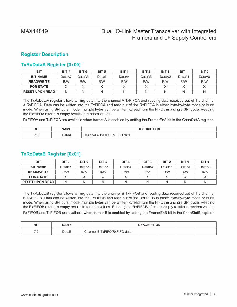
TxRxDataA Register [0x00]
Register Description
TxRxDataB Register [0x01]
BIT BIT 7 BIT 6 BIT 5 BIT 4 BIT 3 BIT 2 BIT 1 BIT 0BIT NAME DataA7 DataA6 Data5 DataA4 DataA3 DataA2 DataA1 DataA0
READ/WRITE R/W R/W R/W R/W R/W R/W R/W R/WPOR STATE X X X X X X X X
RESET UPON READ N N N N N N N N
The TxRxDataA register allows writing data into the channel A TxFIFOA and reading data received out of the channel A RxFIFOA. Data can be written into the TxFIFOA and read out of the RxFIFOA in either byte-by-byte mode or burst mode. When using SPI burst mode, multiple bytes can be written to/read from the FIFOs in a single SPI cycle. Reading the RxFIFOA after it is empty results in random values.RxFIFOA and TxFIFOA are available when framer A is enabled by setting the FramerEnA bit in the ChanStatA register.
BIT NAME DESCRIPTION
7:0 DataA Channel A TxFIFO/RxFIFO data
BIT BIT 7 BIT 6 BIT 5 BIT 4 BIT 3 BIT 2 BIT 1 BIT 0BIT NAME DataB7 DataB6 DataB5 DataB4 DataB3 DataB2 DataB1 DataB0
READ/WRITE R/W R/W R/W R/W R/W R/W R/W R/WPOR STATE X X X X X X X X
RESET UPON READ N N N N N N N N
The TxRxDataB register allows writing data into the channel B TxFIFOB and reading data received out of the channel B RxFIFOB. Data can be written into the TxFIFOB and read out of the RxFIFOB in either byte-by-byte mode or burst mode. When using SPI burst mode, multiple bytes can be written to/read from the FIFOs in a single SPI cycle. Reading the RxFIFOB after it is empty results in random values. Reading the RxFIFOB after it is empty results in random values. RxFIFOB and TxFIFOB are available when framer B is enabled by setting the FramerEnB bit in the ChanStatB register.
BIT NAME DESCRIPTION
7:0 DataB Channel B TxFIFO/RxFIFO data
MAX14819 Dual IO-Link Master Transceiver with Integrated Framers and L+ Supply Controllers
www.maximintegrated.com Maxim Integrated 33
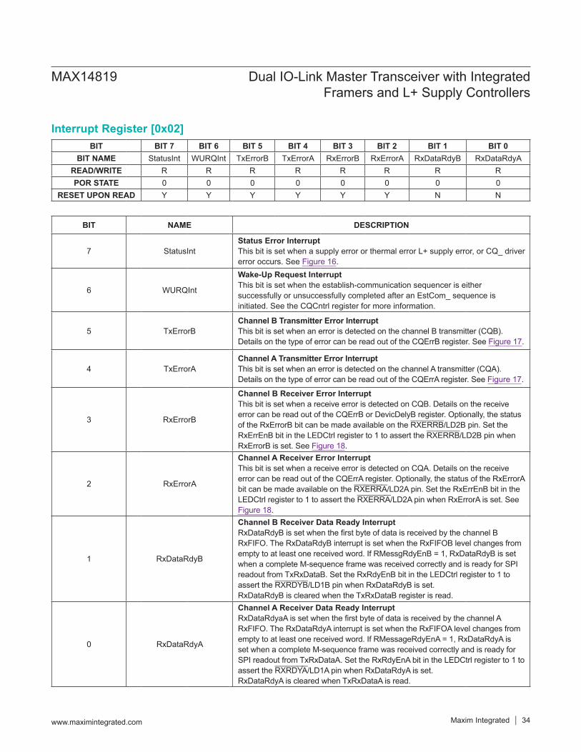
Interrupt Register [0x02]BIT BIT 7 BIT 6 BIT 5 BIT 4 BIT 3 BIT 2 BIT 1 BIT 0
BIT NAME StatusInt WURQInt TxErrorB TxErrorA RxErrorB RxErrorA RxDataRdyB RxDataRdyAREAD/WRITE R R R R R R R RPOR STATE 0 0 0 0 0 0 0 0
RESET UPON READ Y Y Y Y Y Y N N
BIT NAME DESCRIPTION
7 StatusIntStatus Error InterruptThis bit is set when a supply error or thermal error L+ supply error, or CQ_ driver error occurs. See Figure 16.
6 WURQInt
Wake-Up Request InterruptThis bit is set when the establish-communication sequencer is either successfully or unsuccessfully completed after an EstCom_ sequence is initiated. See the CQCntrl register for more information.
5 TxErrorBChannel B Transmitter Error Interrupt This bit is set when an error is detected on the channel B transmitter (CQB). Details on the type of error can be read out of the CQErrB register. See Figure 17.
4 TxErrorAChannel A Transmitter Error Interrupt This bit is set when an error is detected on the channel A transmitter (CQA). Details on the type of error can be read out of the CQErrA register. See Figure 17.
3 RxErrorB
Channel B Receiver Error InterruptThis bit is set when a receive error is detected on CQB. Details on the receive error can be read out of the CQErrB or DevicDelyB register. Optionally, the status of the RxErrorB bit can be made available on the RXERRB/LD2B pin. Set the RxErrEnB bit in the LEDCtrl register to 1 to assert the RXERRB/LD2B pin when RxErrorB is set. See Figure 18.
2 RxErrorA
Channel A Receiver Error InterruptThis bit is set when a receive error is detected on CQA. Details on the receive error can be read out of the CQErrA register. Optionally, the status of the RxErrorA bit can be made available on the RXERRA/LD2A pin. Set the RxErrEnB bit in the LEDCtrl register to 1 to assert the RXERRA/LD2A pin when RxErrorA is set. See Figure 18.
1 RxDataRdyB
Channel B Receiver Data Ready InterruptRxDataRdyBissetwhenthefirstbyteofdataisreceivedbythechannelB RxFIFO. The RxDataRdyB interrupt is set when the RxFIFOB level changes from empty to at least one received word. If RMessgRdyEnB = 1, RxDataRdyB is set when a complete M-sequence frame was received correctly and is ready for SPI readout from TxRxDataB. Set the RxRdyEnB bit in the LEDCtrl register to 1 to assert the RXRDYB/LD1B pin when RxDataRdyB is set.RxDataRdyB is cleared when the TxRxDataB register is read.
0 RxDataRdyA
Channel A Receiver Data Ready InterruptRxDataRdyaAissetwhenthefirstbyteofdataisreceivedbythechannelARxFIFO. The RxDataRdyA interrupt is set when the RxFIFOA level changes from empty to at least one received word. If RMessageRdyEnA = 1, RxDataRdyA is set when a complete M-sequence frame was received correctly and is ready for SPI readout from TxRxDataA. Set the RxRdyEnA bit in the LEDCtrl register to 1 to assert the RXRDYA/LD1A pin when RxDataRdyA is set.RxDataRdyA is cleared when TxRxDataA is read.
MAX14819 Dual IO-Link Master Transceiver with Integrated Framers and L+ Supply Controllers
www.maximintegrated.com Maxim Integrated 34

Figure 16. StatusInt Interrupt Triggers
Figure 18. RxError_Triggers
Figure 17. TxError_ Triggers
VCCUVCORVCCWarnCOR
ThShdnCORThWarnCOR
L+CLimCOR_UVL+COR_
CQFaultCOR_
STAT
US
REG
ISTE
RC
HAN
STAT
_R
EGIS
TER
StatusInt
CQ
Err_
R
EGIS
TER
TransmErr_
TCyclErr_
TChkSmEr_
TSizeErr_
TxError_
ParityErr_
FrameErr_
RSizeErr_
RChkSmErr_
CQ
Erro
r_
REG
ISTE
RS
REGISTER BITS: RxError_
SDO READ BITS: ERRA_
PINS: RXRDY_/LD1_
DelayErr_
Dev
iceD
ly_
REG
ISTE
RS
MAX14819 Dual IO-Link Master Transceiver with Integrated Framers and L+ Supply Controllers
www.maximintegrated.com Maxim Integrated 35
InterruptEn Register [0x03]BIT BIT 7 BIT 6 BIT 5 BIT 4 BIT 3 BIT 2 BIT 1 BIT 0
BIT NAME StatusIntEn WURQIntEn TxErrIntEnB TxErrIntEnA RxErrIntEnB RxErrIntEnA RDaRdyIntEnB RDaRdyIntEnA
READ/WRITE R/W R/W R/W R/W R/W R/W R/W R/WPOR STATE 0 0 0 0 0 0 0 0
RESET UPON READ N N N N N N N N
BIT NAME DESCRIPTION
7 StatusIntEn
Status Interrupt Enable Set the StatIntEn bit to 1 to assert the IRQ output when a StatusInt interrupt is generated.Clear the StatusIntEn bit to disable/mask the IRQ output when a StatusInt interrupt is generated.
6 WURQIntEn
Wake-Up Request Interrupt Enable Set the WURQIntEn bit to 1 to assert the IRQ output when a WURQInt interrupt is generated.Clear the WURQIntEn bit to disable/mask the IRQ output when a WURQInt interrupt is generated.
5 TxErrIntEnB
Channel B Transmitter Error Interrupt EnableSet the TxErrIntEnB bit to 1 to assert the IRQ output when a TxErrorB interrupt is generated.Clear the TxErrIntEn bit to disable/mask the IRQ output when a TxErrorB interrupt is generated.
4 TxErrIntEnA
Channel A Transmitter Error Interrupt EnableSet the TxErrIntEnA bit to 1 to assert the IRQ output when a TxErrorA interrupt is generated. Clear the TxErrIntEn bit to disable/mask the IRQ output when a TxErrorA einterrupt is generated.
3 RxErrIntEnB
Channel B Receiver Error Interrupt EnableSet the RxErrIntEnB bit to 1 to assert the IRQ output when a RxErrorB interrupt is generated.Clear the RxErrIntEnB bit to disable/mask the IRQ output when a RxErrorB interrupt is generated. .The RxErrIntEnB bit does not mask or enable the RXERRB/LD2B pin.
MAX14819 Dual IO-Link Master Transceiver with Integrated Framers and L+ Supply Controllers
www.maximintegrated.com Maxim Integrated 36
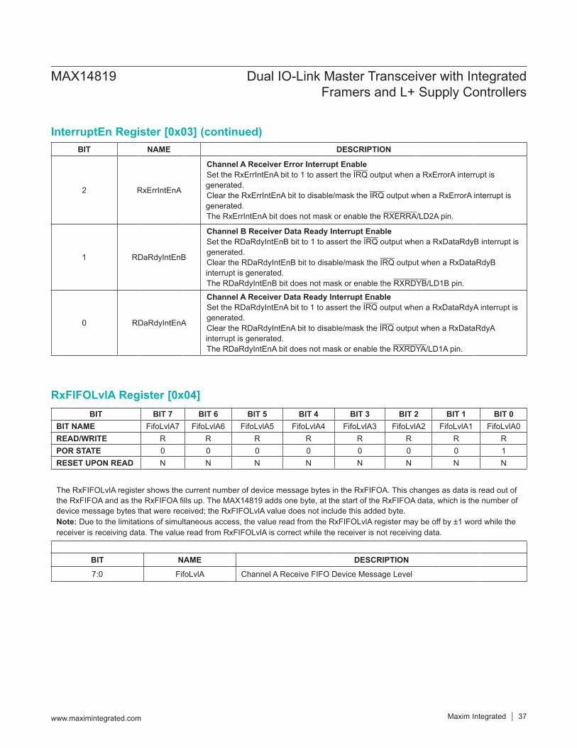
RxFIFOLvlA Register [0x04]
InterruptEn Register [0x03] (continued)
BIT BIT 7 BIT 6 BIT 5 BIT 4 BIT 3 BIT 2 BIT 1 BIT 0BIT NAME FifoLvlA7 FifoLvlA6 FifoLvlA5 FifoLvlA4 FifoLvlA3 FifoLvlA2 FifoLvlA1 FifoLvlA0READ/WRITE R R R R R R R RPOR STATE 0 0 0 0 0 0 0 1RESET UPON READ N N N N N N N N
The RxFIFOLvlA register shows the current number of device message bytes in the RxFIFOA. This changes as data is read out of theRxFIFOAandastheRxFIFOAfillsup.TheMAX14819addsonebyte,atthestartoftheRxFIFOAdata,whichisthenumberofdevice message bytes that were received; the RxFIFOLvlA value does not include this added byte.Note: Due to the limitations of simultaneous access, the value read from the RxFIFOLvlA register may be off by ±1 word while the receiver is receiving data. The value read from RxFIFOLvlA is correct while the receiver is not receiving data.
BIT NAME DESCRIPTION
7:0 FifoLvlA Channel A Receive FIFO Device Message Level
BIT NAME DESCRIPTION
2 RxErrIntEnA
Channel A Receiver Error Interrupt EnableSet the RxErrIntEnA bit to 1 to assert the IRQ output when a RxErrorA interrupt is generated.Clear the RxErrIntEnA bit to disable/mask the IRQ output when a RxErrorA interrupt is generated.The RxErrIntEnA bit does not mask or enable the RXERRA/LD2A pin.
1 RDaRdyIntEnB
Channel B Receiver Data Ready Interrupt EnableSet the RDaRdyIntEnB bit to 1 to assert the IRQ output when a RxDataRdyB interrupt isgenerated. Clear the RDaRdyIntEnB bit to disable/mask the IRQ output when a RxDataRdyB interrupt is generated.The RDaRdyIntEnB bit does not mask or enable the RXRDYB/LD1B pin.
0 RDaRdyIntEnA
Channel A Receiver Data Ready Interrupt EnableSet the RDaRdyIntEnA bit to 1 to assert the IRQ output when a RxDataRdyA interrupt isgenerated. Clear the RDaRdyIntEnA bit to disable/mask the IRQ output when a RxDataRdyA interrupt is generated.The RDaRdyIntEnA bit does not mask or enable the RXRDYA/LD1A pin.
MAX14819 Dual IO-Link Master Transceiver with Integrated Framers and L+ Supply Controllers
www.maximintegrated.com Maxim Integrated 37

RxFIFOLvlB Register [0x05]
CQCtrlA Register [0x06]
BIT BIT 7 BIT 6 BIT 5 BIT 4 BIT 3 BIT 2 BIT 1 BIT 0BIT NAME FifoLvlB7 FifoLvlB6 FifoLvlB5 FifoLvlB4 FifoLvlB3 FifoLvlB2 FifoLvlB1 FifoLvlB0
READ/WRITE R R R R R R R RPOR STATE 0 0 0 0 0 0 0 0
RESET UPON READ N N N N N N N N
The RxFIFOLvlB register shows the current number of device message bytes in the RxFIFOB. This changes as data is read out of theRxFIFOBandastheRxFIFOBfillsup.TheMAX14819addsonebyte,atthestartoftheRxFIFOBdata,whichisthenumberofdevice message bytes that were received; the RxFIFOLvlB value does not include this added byte.Note: Due to the limitations of simultaneous access, the value read from the RxFIFOLvlB register may be off by ±1 word while the receiver is receiving data. The value read from RxFIFOLvlB is correct while the receiver is not receiving data.
BIT NAME DESCRIPTION
7:0 FifoLvlB Channel B Receive FIFO Device Message Level
BIT BIT 7 BIT 6 BIT 5 BIT 4 BIT 3 BIT 2 BIT 1 BIT 0BIT NAME ComRtA1 ComRtA0 EstComA WuPulsA TxFifoRstA RxFifoRstACycleTmrEnA CQSendA
READ/WRITE R/W R/W R/W R/W R/W R/W R/W R/WPOR STATE 0 0 0 0 0 0 0 0
RESET UPON READ N N N N N N N N
BIT NAME DESCRIPTION
[7:6] ComRtA1, ComRtA0
Channel A CQ (CQA) COM Rate Setting The ComRtA[1:0] bits set the COM data rate on the CQA interface. Once the establish-communication sequence, intiated with EstComA, is successfully completed, the COM rate of the IO-link device will be stored in these bits as follows: 00: Detection failure (230.4kbps) 01: COM1 = 4.8kbps 10: COM2 = 38.4kbps 11: COM3 = 230.4kbps
MAX14819 Dual IO-Link Master Transceiver with Integrated Framers and L+ Supply Controllers
www.maximintegrated.com Maxim Integrated 38

CQCtrlA Register [0x06] (continued)BIT NAME DESCRIPTION
5 EstComA
Channel A Establish-Communication Sequence EnableSet the EstComA to 1 to initiate an IO-Link establish-communication se-quence on CQA. After successful completion of the establish communication sequence, a WURQInt interrupt is generated and the EstComA bit changes to 0. During the generated wake-up pulse, the CQA current limit is temporarily set above 500mA internally, although the CL_ register bits are not changed. The COM rate of the IO-Link device is then reflectedbytheComRt0AandComRt1Abitsandthedevicecycletime can be read out of the CyclTimeA register. If the establish-communication sequence was not successful, a WURQInt interrupt is generated and EstComA is 0 and the ComRt1A and ComRt0A bits both = 0. The FramerEnA bit must be 1 to use the EstComA function.
4 WuPulsA
Channel A Wake-Up Pulse Generate Set WuPulsA to 1 to immediately generate a wake-up pulse/request (WURQ) on CQA. Following the wake-up request, the CQA transceiver is set into receive mode. WuPulsA is reset to 0 after the WURQ is completed.WuPulsA is used when the microcontroller manages the establish communication sequence and the EstComA funciton is not used.
3 TxFifoRstA
Channel A TX FIFO (TxFIFOA) ResetSet TxFifoRstA to reset the TxFIFOA. This may be necessary if an SPI transmissionerrorisdetectedwhenfillingtheTxFIFOAorifaCQA transmission error is detected.
2 RxFifoRstAChannel A RX FIFO (RxFIFOA) Reset Set RxFifoRstA to reset the RxFIFOA. This may be necessary if an RSizeErrA event occurs.
1 CycleTmrEnA
Channel A Cycle Timer Enable Set CyclTmrEnA to 1 to enable the channel A cycle time. CyclTmrEnA does not start the cycle timer. Cycle timer A starts when the CQSendA bit is set to 1 (after the timer is enabled) or an associated trigger command is received. Set CyclTmrEnA to 0 to stop the cycle timer. The timer can be stopped at any time, even if the current cycle is not yet complete.
0 CQSendA
Channel A Initiate Master Message Set CQSendA to 1 to initiate transmission of the master message in the channel A transmit FIFO (TxFIFOA). The CQA transceiver is put into transmit mode and sends the master message/data in the TxFIFOA. When the master message is complete/TxFIFOA is empty, the CQA transceiver is set to receive mode to receive device messages.
If CyclTmrEnA = 1, setting CQSendA to 1 also starts cycle timer A. CQSendA is automatically cleared.
MAX14819 Dual IO-Link Master Transceiver with Integrated Framers and L+ Supply Controllers
www.maximintegrated.com Maxim Integrated 39
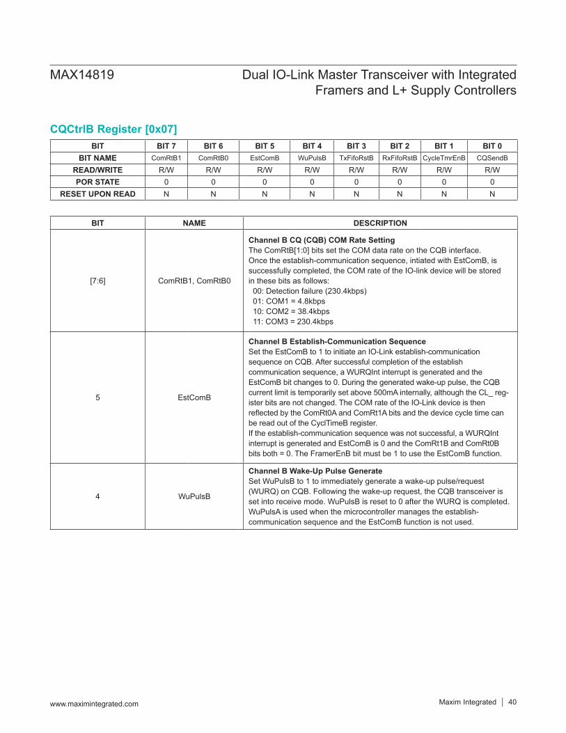
CQCtrlB Register [0x07]BIT BIT 7 BIT 6 BIT 5 BIT 4 BIT 3 BIT 2 BIT 1 BIT 0
BIT NAME ComRtB1 ComRtB0 EstComB WuPulsB TxFifoRstB RxFifoRstB CycleTmrEnB CQSendB
READ/WRITE R/W R/W R/W R/W R/W R/W R/W R/WPOR STATE 0 0 0 0 0 0 0 0
RESET UPON READ N N N N N N N N
BIT NAME DESCRIPTION
[7:6] ComRtB1, ComRtB0
Channel B CQ (CQB) COM Rate Setting The ComRtB[1:0] bits set the COM data rate on the CQB interface. Once the establish-communication sequence, intiated with EstComB, is successfully completed, the COM rate of the IO-link device will be stored in these bits as follows: 00: Detection failure (230.4kbps) 01: COM1 = 4.8kbps 10: COM2 = 38.4kbps 11: COM3 = 230.4kbps
5 EstComB
Channel B Establish-Communication SequenceSet the EstComB to 1 to initiate an IO-Link establish-communication sequence on CQB. After successful completion of the establish communication sequence, a WURQInt interrupt is generated and the EstComB bit changes to 0. During the generated wake-up pulse, the CQB current limit is temporarily set above 500mA internally, although the CL_ reg-ister bits are not changed. The COM rate of the IO-Link device is then reflectedbytheComRt0AandComRt1Abitsandthedevicecycletimecanbe read out of the CyclTimeB register. If the establish-communication sequence was not successful, a WURQInt interrupt is generated and EstComB is 0 and the ComRt1B and ComRt0B bits both = 0. The FramerEnB bit must be 1 to use the EstComB function.
4 WuPulsB
Channel B Wake-Up Pulse Generate Set WuPulsB to 1 to immediately generate a wake-up pulse/request (WURQ) on CQB. Following the wake-up request, the CQB transceiver is set into receive mode. WuPulsB is reset to 0 after the WURQ is completed.WuPulsA is used when the microcontroller manages the establish- communication sequence and the EstComB function is not used.
MAX14819 Dual IO-Link Master Transceiver with Integrated Framers and L+ Supply Controllers
www.maximintegrated.com Maxim Integrated 40
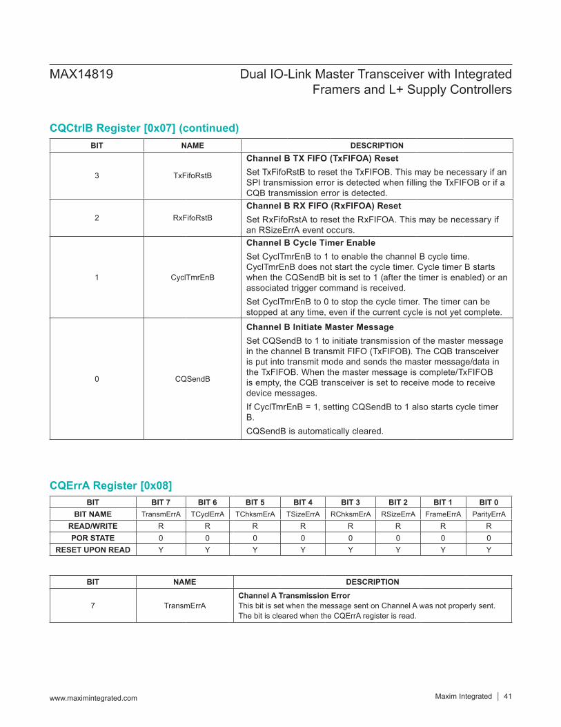
CQCtrlB Register [0x07] (continued)
CQErrA Register [0x08]
BIT NAME DESCRIPTION
3 TxFifoRstB
Channel B TX FIFO (TxFIFOA) ResetSet TxFifoRstB to reset the TxFIFOB. This may be necessary if an SPI transmission error is detected when filling the TxFIFOB or if a CQB transmission error is detected.
2 RxFifoRstBChannel B RX FIFO (RxFIFOA) ResetSet RxFifoRstA to reset the RxFIFOA. This may be necessary if an RSizeErrA event occurs.
1 CyclTmrEnB
Channel B Cycle Timer Enable Set CyclTmrEnB to 1 to enable the channel B cycle time. CyclTmrEnB does not start the cycle timer. Cycle timer B starts when the CQSendB bit is set to 1 (after the timer is enabled) or an associated trigger command is received. Set CyclTmrEnB to 0 to stop the cycle timer. The timer can be stopped at any time, even if the current cycle is not yet complete.
0 CQSendB
Channel B Initiate Master MessageSet CQSendB to 1 to initiate transmission of the master message in the channel B transmit FIFO (TxFIFOB). The CQB transceiver is put into transmit mode and sends the master message/data in the TxFIFOB. When the master message is complete/TxFIFOB is empty, the CQB transceiver is set to receive mode to receive device messages. If CyclTmrEnB = 1, setting CQSendB to 1 also starts cycle timer B. CQSendB is automatically cleared.
BIT BIT 7 BIT 6 BIT 5 BIT 4 BIT 3 BIT 2 BIT 1 BIT 0BIT NAME TransmErrA TCyclErrA TChksmErA TSizeErrA RChksmErA RSizeErrA FrameErrA ParityErrA
READ/WRITE R R R R R R R RPOR STATE 0 0 0 0 0 0 0 0
RESET UPON READ Y Y Y Y Y Y Y Y
BIT NAME DESCRIPTION
7 TransmErrAChannel A Transmission ErrorThis bit is set when the message sent on Channel A was not properly sent. The bit is cleared when the CQErrA register is read.
MAX14819 Dual IO-Link Master Transceiver with Integrated Framers and L+ Supply Controllers
www.maximintegrated.com Maxim Integrated 41
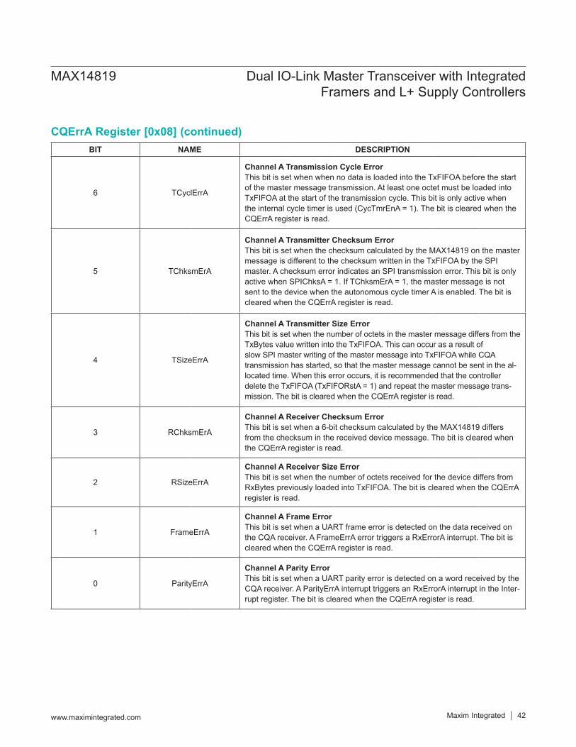
CQErrA Register [0x08] (continued)BIT NAME DESCRIPTION
6 TCyclErrA
Channel A Transmission Cycle ErrorThis bit is set when when no data is loaded into the TxFIFOA before the start of the master message transmission. At least one octet must be loaded into TxFIFOA at the start of the transmission cycle. This bit is only active when the internal cycle timer is used (CycTmrEnA = 1). The bit is cleared when the CQErrA register is read.
5 TChksmErA
Channel A Transmitter Checksum ErrorThis bit is set when the checksum calculated by the MAX14819 on the master message is different to the checksum written in the TxFIFOA by the SPI master. A checksum error indicates an SPI transmission error. This bit is only active when SPIChksA = 1. If TChksmErA = 1, the master message is not sent to the device when the autonomous cycle timer A is enabled. The bit is cleared when the CQErrA register is read.
4 TSizeErrA
Channel A Transmitter Size ErrorThis bit is set when the number of octets in the master message differs from the TxBytes value written into the TxFIFOA. This can occur as a result of slow SPI master writing of the master message into TxFIFOA while CQA transmission has started, so that the master message cannot be sent in the al-located time. When this error occurs, it is recommended that the controller delete the TxFIFOA (TxFIFORstA = 1) and repeat the master message trans-mission. The bit is cleared when the CQErrA register is read.
3 RChksmErA
Channel A Receiver Checksum Error This bit is set when a 6-bit checksum calculated by the MAX14819 differs from the checksum in the received device message. The bit is cleared when the CQErrA register is read.
2 RSizeErrA
Channel A Receiver Size ErrorThis bit is set when the number of octets received for the device differs from RxBytes previously loaded into TxFIFOA. The bit is cleared when the CQErrA register is read.
1 FrameErrA
Channel A Frame ErrorThis bit is set when a UART frame error is detected on the data received on the CQA receiver. A FrameErrA error triggers a RxErrorA interrupt. The bit is cleared when the CQErrA register is read.
0 ParityErrA
Channel A Parity ErrorThis bit is set when a UART parity error is detected on a word received by the CQA receiver. A ParityErrA interrupt triggers an RxErrorA interrupt in the Inter-rupt register. The bit is cleared when the CQErrA register is read.
MAX14819 Dual IO-Link Master Transceiver with Integrated Framers and L+ Supply Controllers
www.maximintegrated.com Maxim Integrated 42
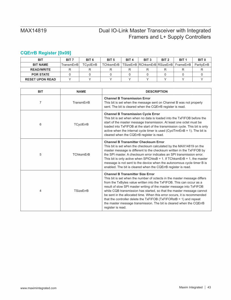
CQErrB Register [0x09]BIT BIT 7 BIT 6 BIT 5 BIT 4 BIT 3 BIT 2 BIT 1 BIT 0
BIT NAME TransmErrB TCyclErrB TChksmErB TSizeErrB RChksmErB RSizeErrB FrameErrB ParityErrBREAD/WRITE R R R R R R R RPOR STATE 0 0 0 0 0 0 0 0
RESET UPON READ Y Y Y Y Y Y Y Y
BIT NAME DESCRIPTION
7 TransmErrBChannel B Transmission ErrorThis bit is set when the message sent on Channel B was not properly sent. The bit is cleared when the CQErrB register is read.
6 TCyclErrB
Channel B Transmission Cycle Error This bit is set when when no data is loaded into the TxFIFOB before the start of the master message transmission. At least one octet must be loaded into TxFIFOB at the start of the transmission cycle. This bit is only active when the internal cycle timer is used (CyclTmrEnB = 1). The bit is cleared when the CQErrB register is read.
5 TChksmErB
Channel B Transmitter Checksum ErrorThis bit is set when the checksum calculated by the MAX14819 on the master message is different to the checksum written in the TxFIFOB by the SPI master. A checksum error indicates an SPI transmission error. This bit is only active when SPIChksB = 1. If TChksmErB = 1, the master message is not sent to the device when the autonomous cycle timer B is enabled. The bit is cleared when the CQErrB register is read.
4 TSizeErrB
Channel B Transmitter Size ErrorThis bit is set when the number of octects in the master message differs from the TxBytes value written into the TxFIFOB. This can occur as a result of slow SPI master writing of the master message into TxFIFOB while CQB transmission has started, so that the master message cannot be sent in the allocated time. When this error occurs, it is recommended that the controller delete the TxFIFOB (TxFIFORstB = 1) and repeat the master message transmission. The bit is cleared when the CQErrB register is read.
MAX14819 Dual IO-Link Master Transceiver with Integrated Framers and L+ Supply Controllers
www.maximintegrated.com Maxim Integrated 43
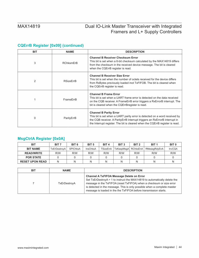
MsgCtrlA Register [0x0A]
CQErrB Register [0x09] (continued)
BIT BIT 7 BIT 6 BIT 5 BIT 4 BIT 3 BIT 2 BIT 1 BIT 0BIT NAME TxErDestroyA SPIChksA InsChksA TSizeEnA TxKeepMsgA RChksEnA RMessgRdyEnA InvCQA
READ/WRITE R/W R/W R/W R/W R/W R/W R/W R/WPOR STATE 0 0 0 0 0 0 0 0
RESET UPON READ N N N N N N N N
BIT NAME DESCRIPTION
7 TxErDestroyA
Channel A TxFIFOA Message Delete on ErrorSet TxErDestroyA = 1 to instruct the MAX14819 to automatically delete the message in the TxFIFOA (reset TxFIFOA) when a checksum or size error is detected in the message. This is only possible when a complete master message is loaded in the the TxFIFOA before transmission starts.
BIT NAME DESCRIPTION
3 RChksmErB
Channel B Receiver Checksum Error This bit is set when a 6-bit checksum calculated by the MAX14819 differs from the checksum in the received device message. The bit is cleared when the CQErrB register is read.
2 RSizeErrB
Channel B Receiver Size ErrorThis bit is set when the number of octets received for the device differs from RxBytes previously loaded inot TxFIFOB. The bit is cleared when the CQErrB register is read.
1 FrameErrB
Channel B Frame ErrorThis bit is set when a UART frame error is detected on the data received on the CQB receiver. A FrameErrB error triggers a RxErrorB interrupt. The bit is cleared when the CQErrBregister is read.
0 ParityErrB
Channel B Parity ErrorThis bit is set when a UART parity error is detected on a word received by the CQB receiver. A ParityErrB interrupt triggers an RxErrorB interrupt in the Interrupt register. The bit is cleared when the CQErrB register is read.
MAX14819 Dual IO-Link Master Transceiver with Integrated Framers and L+ Supply Controllers
www.maximintegrated.com Maxim Integrated 44

MsgCtrlA Register [0x0A] (continued)BIT NAME DESCRIPTION
6 SPIChksA
Channel A SPI Checksum Verify Set SPIChksA = 1 to enable checking of the SPI checksum that the SPI master wrote into the CKT octet compared to the calculated checksum. This bit is independent of InsChksA. When a checksum disparity is found, the TChksmErA bit is set in the CQErrA register.
5 InsChksA
Channel A Insert ChecksumSet InsChksA = 1 to instruct the MAX14819 to calculate the 6-bit checksum on the master message residing in TxFIFOA and insert this into the CKT byte. The bits written by the SPI master into these 6 bits are replaced.
4 TSizeEnA
Channel A TxFIFOA Size Check EnableSet TSizeEnA = 1 to require the MAX14819 to verify that the number of bytes in the TxFIFOA is equal to the TxBytes value written into the TxFIFOA. If the master message is loaded before transmission starts, a TxErrA interrupt is generated and the message can be deleted by the MAX14819 (when TxErDestroyA = 1). If the transmission has started before the whole message is loaded, then the message cannot be automatically deleted.
3 TxKeepMsgA
Channel A Keep TxFIFO Message EnableSet TxKeepMsgA = 1 to stop the MAX14819 from clearing the TxFIFOA after the message has been sent. This allows sending the same master message on the following cycle. When TxKeepMsgA = 0, the data in the TxFIFOA is automatically cleared after the message has been sent.
2 RChksEnA
Channel A Device Message Checksum EnableSet RChksEnA = 1 to enable the MAX14819 to check the device message checksum in the RxFIFOA. If an error is detected during the checksum check, the RChksmErA bit is set.
1 RMessgRdyEnA
Channel A Received Message ReadySet RMessgRdyEnA = 1 to generate a RxDataRdyA interrupt when the complete device response message is received and has no errors. When RMessgRdyEnA = 0, a RxDataRdyA interrupt is generated as soon as the firstwordisreceivedintheRxFIFOA.
0 InvCQA
Channel A Logic Invert Set InvCQA = 1 to switch the polarity of the CQA output for transmission and reception. when InvCQA = 0, TXA and RXA are logic inverts of CQA. When InvCQA = 1, TXA and RXA follow CQA, logically.
MAX14819 Dual IO-Link Master Transceiver with Integrated Framers and L+ Supply Controllers
www.maximintegrated.com Maxim Integrated 45

MsgCtrlB [0x0B]BIT BIT 7 BIT 6 BIT 5 BIT 4 BIT 3 BIT 2 BIT 1 BIT 0
BIT NAME TxErDestroyB SPIChksB InsChksB TSizeEnB TxKeepMsgB RChksEnb RMessgRdyEnb InvCQBREAD/WRITE R/W R/W R/W R/W R/W R/W R/W R/WPOR STATE 0 0 0 0 0 0 0 0
RESET UPON READ N N N N N N N N
BIT NAME DESCRIPTION
7 TxErDestroyB
Channel B TxFIFOB Message Delete on ErrorSet TxErDestroyB = 1 to instruct the MAX14819 to automatically delete the message in the TxFIFOB (reset TxFIFOB) when a checksum or size error is detected in the message. This is only possible when a complete master message is loaded in the the TxFIFO before transmission starts.
6 SPIChksB
Channel B SPI Checksum Verify Set SPIChksB = 1 to enable checking of the SPI checksum that the SPI master wrote into the CKT octet compared to the calculated checksum. This bit is independent of InsChksB. When a checksum disparity is found, the TChksmErB bit is set in the CQErrB register.
5 InsChksB
Channel B Insert ChecksumSet InsChksB = 1 to instruct the MAX14819 to calculate the 6-bit checksum on the master message residing in TxFIFOB and inster this into the CKT byte. The bits written by the SPI master into these 6 bits are replaced.
4 TSizeEnB
Channel B TxFIFOB Size Check Enable Set TSizeEnB = 1 to require the MAX14819 to verify that the number of bytes in the TxFIFOB is equal to the TxBytes value written into the TxFIFOB. If the master message is loaded before transmission starts, a TxErrB interrupt is generated and the message can be deleted by the MAX14819 (when TxErDestroyB = 1). If the transmission has started before the whole message is loaded, then the message cannot be automatically deleted.
MAX14819 Dual IO-Link Master Transceiver with Integrated Framers and L+ Supply Controllers
www.maximintegrated.com Maxim Integrated 46
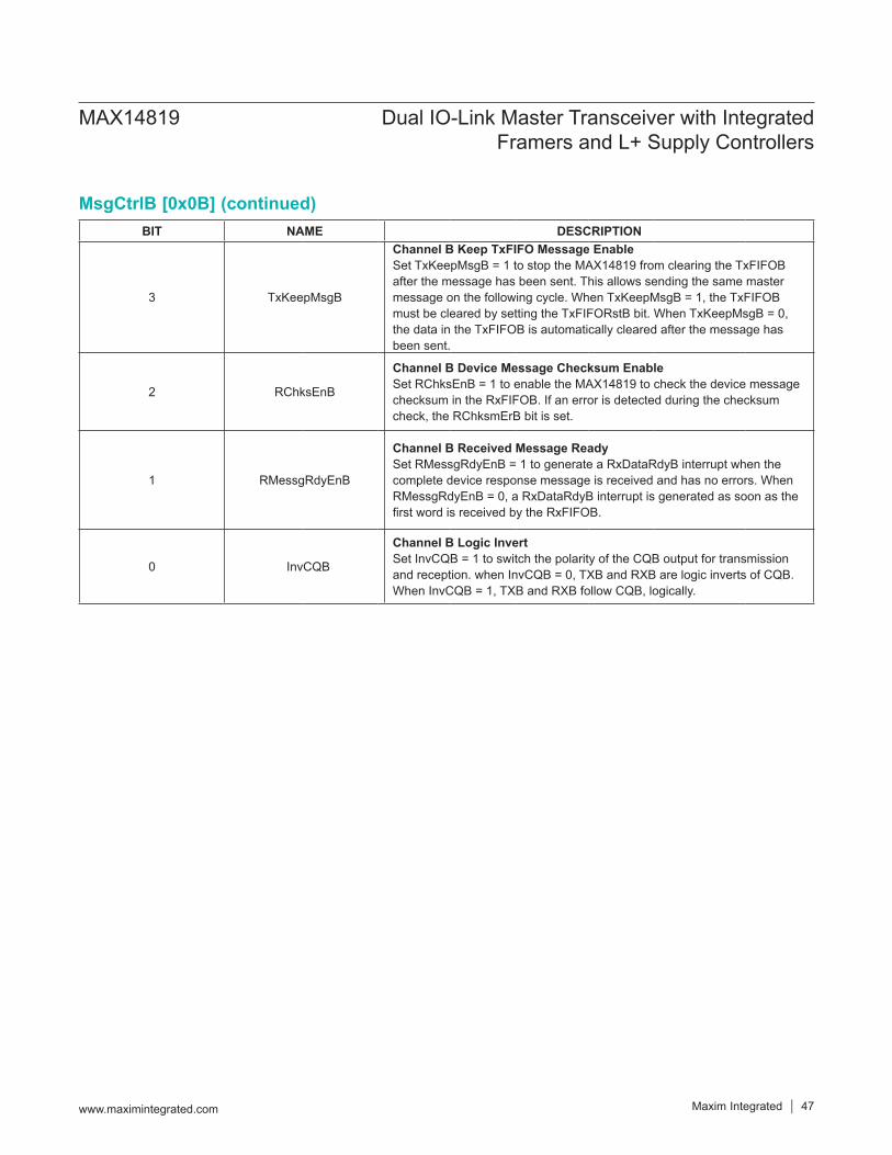
MsgCtrlB [0x0B] (continued)BIT NAME DESCRIPTION
3 TxKeepMsgB
Channel B Keep TxFIFO Message EnableSet TxKeepMsgB = 1 to stop the MAX14819 from clearing the TxFIFOB after the message has been sent. This allows sending the same master message on the following cycle. When TxKeepMsgB = 1, the TxFIFOB must be cleared by setting the TxFIFORstB bit. When TxKeepMsgB = 0, the data in the TxFIFOB is automatically cleared after the message has been sent.
2 RChksEnB
Channel B Device Message Checksum EnableSet RChksEnB = 1 to enable the MAX14819 to check the device message checksum in the RxFIFOB. If an error is detected during the checksum check, the RChksmErB bit is set.
1 RMessgRdyEnB
Channel B Received Message ReadySet RMessgRdyEnB = 1 to generate a RxDataRdyB interrupt when the complete device response message is received and has no errors. When RMessgRdyEnB = 0, a RxDataRdyB interrupt is generated as soon as the firstwordisreceivedbytheRxFIFOB.
0 InvCQB
Channel B Logic Invert Set InvCQB = 1 to switch the polarity of the CQB output for transmission and reception. when InvCQB = 0, TXB and RXB are logic inverts of CQB. When InvCQB = 1, TXB and RXB follow CQB, logically.
MAX14819 Dual IO-Link Master Transceiver with Integrated Framers and L+ Supply Controllers
www.maximintegrated.com Maxim Integrated 47

ChanStatA Register [0x0C]BIT BIT 7 BIT 6 BIT 5 BIT 4 BIT 3 BIT 2 BIT 1 BIT 0
BIT NAME RstA FramerEnA L+CLimCORA UVL+CORA CQFaultCORA L+CLimA UVL+A CQFaultAREAD/WRITE R/W R/W R R R R R RPOR STATE 0 0 X X 0 X X 0
RESET UPON READ N N Y Y Y N N N
BIT NAME DESCRIPTION
7 RstA
Channel A Register ResetSet RstA = 1 to reset all channel A register bits, the TxFIFOA, and RxFIFOA. Channel B registers and global register bits are not affected. RstA is cleared automatically when the channel A registers have been reset.
6 FramerEnA
Channel A Framer EnableSet FramerEnA = 1 to enable the internal message handler, RxFIFOA, and TxFIFOA. When an external UART is used (the internal framer is not used), set FramerEnA = 0 and connect the external UART to the TXENA, TXA, and RXA pins.
5 L+CLimCORA
Channel A L+A Current Limit LatchedClear-on-readflagoftheL+ClimAbit.ThisbitissetonlywhentheL+CLimA bit transitions from 0 to 1. This bit can generate a StatusInt interrupt.
4 UVL+CORAChannel A L+A UnderVoltage LatchedClear-on-readflagoftheUVL+Abit.ThisbitissetonlywhentheUVL+Abit transitions from 0 to 1. This bit can generate a StatusInt interrupt.
3 CQFaultCORA
Channel A CQ Driver Fault LatchedClear-on-readflagoftheCQFaultAbit.ThisbitissetonlywhentheCQFaultA bit transitions from 0 to 1. This bit can generate a StatusInt interrupt.
2 L+CLimA
Channel A L+A Current Limit Real TimeThis bit is set when the L+A sensor supply load current exceeds the current-limit threshold set by the sense resistor for longer than the programmed current-limit blanking time (see the L+CnfgA register for more information). L+CLimA is cleared when the L+A supply exits autoretry current limiting.
1 UVL+AChannel A L+A Undervoltage Real TimeThis bit is set when the L+A supply voltage falls below 18V (typ). The bit is cleared when the L+A voltage rises above 18V (typ).
0 CQFaultA
Channel A CQ Driver Fault Real TimeThis bit is set when a fault is detected on the CQA driver. The fault can be an overload condition, for example an overcurrent of thermal-shutdown event.
MAX14819 Dual IO-Link Master Transceiver with Integrated Framers and L+ Supply Controllers
www.maximintegrated.com Maxim Integrated 48
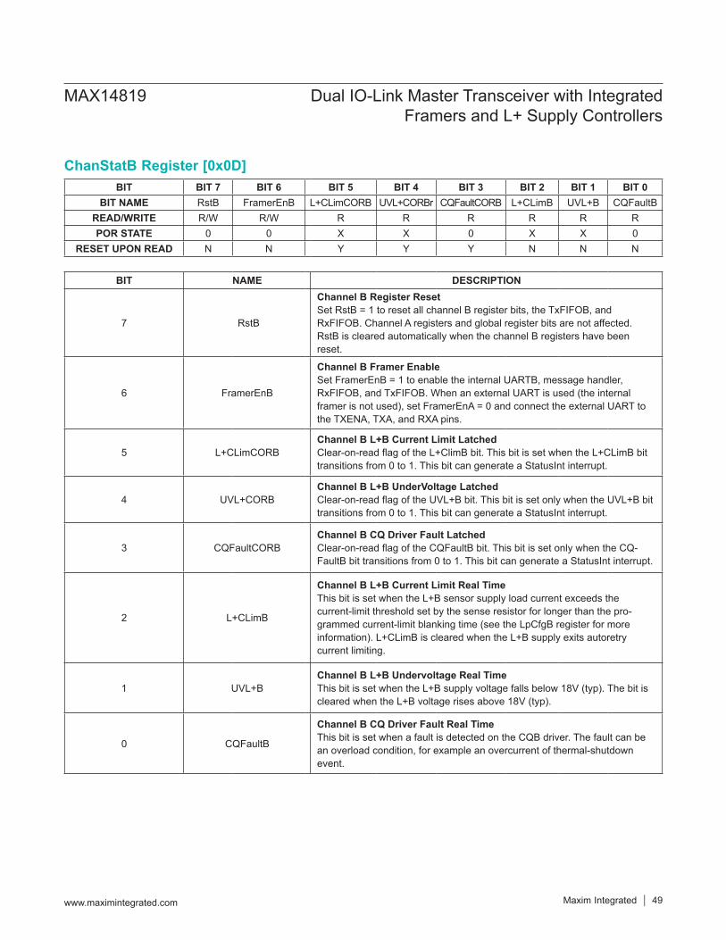
ChanStatB Register [0x0D]BIT BIT 7 BIT 6 BIT 5 BIT 4 BIT 3 BIT 2 BIT 1 BIT 0
BIT NAME RstB FramerEnB L+CLimCORB UVL+CORBr CQFaultCORB L+CLimB UVL+B CQFaultBREAD/WRITE R/W R/W R R R R R RPOR STATE 0 0 X X 0 X X 0
RESET UPON READ N N Y Y Y N N N
BIT NAME DESCRIPTION
7 RstB
Channel B Register ResetSet RstB = 1 to reset all channel B register bits, the TxFIFOB, and RxFIFOB. Channel A registers and global register bits are not affected. RstB is cleared automatically when the channel B registers have been reset.
6 FramerEnB
Channel B Framer EnableSet FramerEnB = 1 to enable the internal UARTB, message handler, RxFIFOB, and TxFIFOB. When an external UART is used (the internal framer is not used), set FramerEnA = 0 and connect the external UART to the TXENA, TXA, and RXA pins.
5 L+CLimCORBChannel B L+B Current Limit LatchedClear-on-readflagoftheL+ClimBbit.ThisbitissetwhentheL+CLimBbittransitions from 0 to 1. This bit can generate a StatusInt interrupt.
4 UVL+CORBChannel B L+B UnderVoltage LatchedClear-on-readflagoftheUVL+Bbit.ThisbitissetonlywhentheUVL+Bbittransitions from 0 to 1. This bit can generate a StatusInt interrupt.
3 CQFaultCORBChannel B CQ Driver Fault Latched Clear-on-readflagoftheCQFaultBbit.ThisbitissetonlywhentheCQ-FaultB bit transitions from 0 to 1. This bit can generate a StatusInt interrupt.
2 L+CLimB
Channel B L+B Current Limit Real TimeThis bit is set when the L+B sensor supply load current exceeds the current-limit threshold set by the sense resistor for longer than the pro-grammed current-limit blanking time (see the LpCfgB register for more information). L+CLimB is cleared when the L+B supply exits autoretry current limiting.
1 UVL+BChannel B L+B Undervoltage Real TimeThis bit is set when the L+B supply voltage falls below 18V (typ). The bit is cleared when the L+B voltage rises above 18V (typ).
0 CQFaultB
Channel B CQ Driver Fault Real TimeThis bit is set when a fault is detected on the CQB driver. The fault can be an overload condition, for example an overcurrent of thermal-shutdown event.
MAX14819 Dual IO-Link Master Transceiver with Integrated Framers and L+ Supply Controllers
www.maximintegrated.com Maxim Integrated 49

LEDCtrl Register [0x0E]BIT BIT 7 BIT 6 BIT 5 BIT 4 BIT 3 BIT 2 BIT 1 BIT 0
BIT NAME LEDEn2B RxErrEnB LEDEn1B RxRdyEnB LEDEn2A RxErrEnA LEDEn1A RxRdyEnAREAD/WRITE R/W R/W R/W R/W R/W R/W R/W R/WPOR STATE 0 0 0 0 0 0 0 0
RESET UPON READ N N N N N N N N
BIT NAME DESCRIPTION
7 LEDEn2B
Channel B LD2B LED Driver ControlSet LEDEn2B = 1 to turn on a LED connected to RXERRB/LD2B. Set LEDEn2B = 0 to turn the LED off. LEDEn2B is only active when RxErrEnB = 0.
6 RxErrEnB
Channel B RXERRB/LD2B Pin Function SelectSet RxErrEnB = 1 to enable the receiver-error (RxErrorB) interrupt functionality on the RXERRB/LD2B pin. In this mode, RXERRB/LD2B asserts when the RxErrorB bit is set. The RXERRB/LD2B pin functionality is not affected by the RxErrIntEnB interrupt mask.Set RxErrEnB = 0 to enable the LED driver function on the ERRB/LD2B output.
5 LEDEn1B
Channel B LD1B LED Driver ControlSet LEDEn1B = 1 to turn on a LED connected to RXRDYB/LD1B. Set LEDEn1B = 0 to turn the LED off. LEDEn1B is only active when RxRdyEnB = 0.
4 RxRdyEnB
Channel B RXRDYB/LD1B Pin Function SelectSet RxRdyEnB = 1 to enable the receiver-error (RxErrorB) interrupt functionality on the RXRDYB/LD1B pin. In this mode, RXRDYB/LD1B asserts when the RcDaRdyB bit is set. The RXRDYB/LD1B pin functionality is not affected by the RxDaRdyIntEnB interrupt mask.Set RxRdyEnB = 0 to enable the LED driver function on the RXRDYB/LD1B pin.
3 LEDEn2A
Channel A LD2A LED Driver ControlSet LEDEn2A = 1 to turn on a LED connected to RXERRA/LD2A. Set LEDEn2A = 0 to turn the LED off. LEDEn2A is only active when RxErrEnA = 0.
MAX14819 Dual IO-Link Master Transceiver with Integrated Framers and L+ Supply Controllers
www.maximintegrated.com Maxim Integrated 50
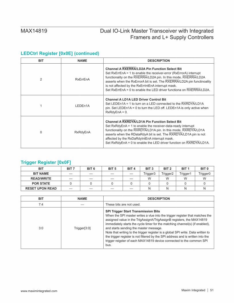
LEDCtrl Register [0x0E] (continued)
Trigger Register [0x0F]BIT BIT 7 BIT 6 BIT 5 BIT 4 BIT 3 BIT 2 BIT 1 BIT 0
BIT NAME — — — — Trigger3 Trigger2 Trigger1 Trigger0READ/WRITE — — — — W W W WPOR STATE 0 0 0 0 0 0 0 0
RESET UPON READ — — — — N N N N
BIT NAME DESCRIPTION
7:4 — These bits are not used.
3:0 Trigger[3:0]
SPI Trigger Start Transmission Bits When the SPI master writes a vlue into the trigger register that matches the assigned value in the TrigAssignA/TrigAssignB registers, the MAX14819 immediately starts the cycle timer for the matching channel(s) (if enabled), and starts sending the master message.Note that writing to the trigger register is a global SPI write. Data written to thetriggerregisterisnotfilteredbytheSPIaddressandiswrittenintothetrigger reigster of each MAX14819 device connected to the common SPI bus.
BIT NAME DESCRIPTION
2 RxErrEnA
Channel A RXERRA/LD2A Pin Function Select BitSet RxErrEnA = 1 to enable the receiver-error (RxErrorA) interrupt functionality on the RXERRA/LD2A pin. In this mode, RXERRA/LD2A asserts when the RxErrorA bit is set. The RXERRA/LD2A pin functinoality is not affected by the RxErrIntEnA interrupt mask.Set RxErrEnA = 0 to enable the LED driver functiona on RXERRA/LD2A.
1 LEDEn1A
Channel A LD1A LED Driver Control BitSet LEDEn1A = 1 to turn on a LED connected to the RXRDYA/LD1A pin. Set LEDEn1A = 0 to turn the LED off. LEDEn1A is only active when RxRdyEnA = 0.
0 RxRdyEnA
Channel A RXRDYA/LD1A Pin Function Select BitSet RxRdyEnA = 1 to enable the receiver-data-ready interrupt functionality on the RXRDYA/LD1A pin. In this mode, RXRDYA/LD1A asserts when the RDataRdyA bit is set. The RXRDYA/LD1A pin is not affected by the RxDaRdyIntEnA interrupt mask.Set RxRdyEnA = 0 to enable the LED driver function on RXRDYA/LD1A.
MAX14819 Dual IO-Link Master Transceiver with Integrated Framers and L+ Supply Controllers
www.maximintegrated.com Maxim Integrated 51

CQCfgA Register [0x10]BIT BIT 7 BIT 6 BIT 5 BIT 4 BIT 3 BIT 2 BIT 1 BIT 0
BIT NAME IEC3ThA SourceSinkA SinkSelA1 SinkSelA0 NPNA PushPulA DrvDisA CQFilterEnAREAD/WRITE R/W R/W R/W R/W R/W R/W R/W R/WPOR STATE 0 0 0 0 0 0 1 0
RESET UPON READ N N N N N N N N
BIT NAME DESCRIPTION
7 IEC3ThA
Channel A IEC61131-2 Type2/3 Threshold Select Set IEC3ThA = 0 for IO-Link operation and to select IEC61131-2 type 1 thresholds in SIO digital input mode. Set IEC3ThA = 1 to enable type 2/3 thresholds on receiver CQA, if desired for SIO digital input operation.
6 SourceSinkA
Channel A CQ Current Sink or Source Select Set SourceSinkA = 1 to enable the internal current source on CQA. Set SourceSinkA = 0 to enable the internal current sink on CQA. Select the current level with the SinkSelA[1:0] bits.
5:4 SinkSelA[1:0]
Channel A CQ Sink/Source Current Level SelectSet the SinkSelA[1:0] bits to enable/disable and select the current level of the internal current sink or source on CQA: 00: Current sink/source OFF 01: 5mA 10: 2mA11:150μA
3 NPNAChannel A CQ Driver NPN/PNP Mode SelectSetNPNA=1toconfiguretheCQAdriverinNPNmode.SetNPNA=0toconfiguretheCQAdriverinPNPmode.NPNAisignoredifPushPulA=1.
2 PushPulA
Channel A CQ Driver Push-Pull Mode SelectSetPushPulA=1toconfiguretheCQAdriverinpush-pullmoderequiredfor IO-Link operation. Set PushPulA = 0 for open-drain operation (NPN or PNP) on the CQA driver.
1 DrvDisAChannel A CQ Driver DisableSet DrvDisA = 1 to disable the CQA driver. CQA is high impedance when disabled. Set DrvDisA = 0 to enable the CQA driver.
0 CQFilterEnA
Channel A CQ Glitch Filter EnableSetCQFilterEnA=1toenabletheglitchfilterontheCQAreceiver.Thisisusefulforburstfiltering.Transientslongerthan1.3µs(typ)areignoredwhentheglitchfilterisenabled.
MAX14819 Dual IO-Link Master Transceiver with Integrated Framers and L+ Supply Controllers
www.maximintegrated.com Maxim Integrated 52

CQCfgB Register [0x11]BIT BIT 7 BIT 6 BIT 5 BIT 4 BIT 3 BIT 2 BIT 1 BIT 0
BIT NAME IEC3ThB SourceSinkB SinkSelB1 SinkSelB0 NPNB PushPulB DrvDisB CQFilterEnBREAD/WRITE R/W R/W R/W R/W R/W R/W R/W R/WPOR STATE 0 0 0 0 0 0 1 0
RESET UPON READ N N N N N N N N
BIT NAME DESCRIPTION
7 IEC3ThB
Channel B IEC61131-2 Type2/3 Threshold SelectSet IEC3ThB = 0 for IO-Link operation and to select IEC61131-2 type 1 thresholds in SIO digital input mode. Set IEC3ThB = 1 to enable type 2/3 thresholds on receiver CQB, if desired for SIO digital input operation.
6 SourceSinkB
Channel B CQ Current Sink or Source Select Set SourceSinkB = 1 to enable the internal current source on CQB. Set SourceSinkB = 0 to enable the internal current sink on CQB. Select the current level with the SinkSelB[1:0] bits.
5:4 SinkSelB[1:0]
Channel B CQ Sink/Source Current Level SelectSet the SinkSelB[1:0] bits to enable/disable and select the current level of the internal current sink or source on CQB: 00: Current sink/source OFF 01: 5mA 10: 2mA11:150μA
3 NPNBChannel B CQ Driver NPN/PNP Mode SelectSetNPNB=1toconfiguretheCQBdriverinNPN mode. Set NPNB = 0 to configuretheCQBdriverinPNP mode. NPNB is ignored if PushPulB = 1.
2 PushPulB
Channel B CQ Driver Push-Pull Mode SelectSetPushPulB=1toconfiguretheCQBdriverinpush-pullmoderequiredfor IO-Link operation. Set PushPulB = 0 for open-drain operation (NPN or PNP) on the CQB driver.
1 DrvDisBChannel B CQ Driver DisableSet DrvrDisB = 1 to disable the CQB driver. CQB is high impedance when disabled. Set DrvrDisB = 0 to enable the CQB driver.
0 CQFilterEnB
Channel B CQ Glitch Filter EnableSetCQFilterEnB=1toenabletheglitchfilterontheCQBreceiver.Thisisusefulforburstfiltering.Transientslongerthan1.3µs(typ)areignoredwhentheglitchfilterisenabled.
MAX14819 Dual IO-Link Master Transceiver with Integrated Framers and L+ Supply Controllers
www.maximintegrated.com Maxim Integrated 53
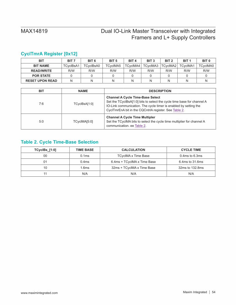
CyclTmrA Register [0x12]
Table 2. Cycle Time-Base Selection
BIT BIT 7 BIT 6 BIT 5 BIT 4 BIT 3 BIT 2 BIT 1 BIT 0BIT NAME TCyclBsA1 TCyclBsA0 TCyclMA5 TCyclMA4 TCyclMA3 TCyclMA2 TCyclMA1 TCyclMA0
READ/WRITE R/W R/W R/W R/W R/W R/W R/W R/WPOR STATE 0 0 0 0 0 0 0 0
RESET UPON READ N N N N N N N N
BIT NAME DESCRIPTION
7:6 TCyclBsA[1:0]
Channel A Cycle Time-Base SelectSet the TCyclBsA[1:0] bits to select the cycle time base for channel A IO-Link communication. The cycle timer is enabled by setting the CyclTmrEnA bit in the CQCntrlA register. See Table 2.
5:0 TCyclMA[5:0]Channel A Cycle Time MultiplerSet the TCyclMA bits to select the cycle time multiplier for channel A communication. ee Table 2.
TCyclBs_[1:0] TIME BASE CALCULATION CYCLE TIME
00 0.1ms TCyclMA x Time Base 0.4ms to 6.3ms
01 0.4ms 6.4ms + TCyclMA x Time Base 6.4ms to 31.6ms
10 1.6ms 32ms + TCyclMA x Time Base 32ms to 132.8ms
11 N/A N/A N/A
MAX14819 Dual IO-Link Master Transceiver with Integrated Framers and L+ Supply Controllers
www.maximintegrated.com Maxim Integrated 54
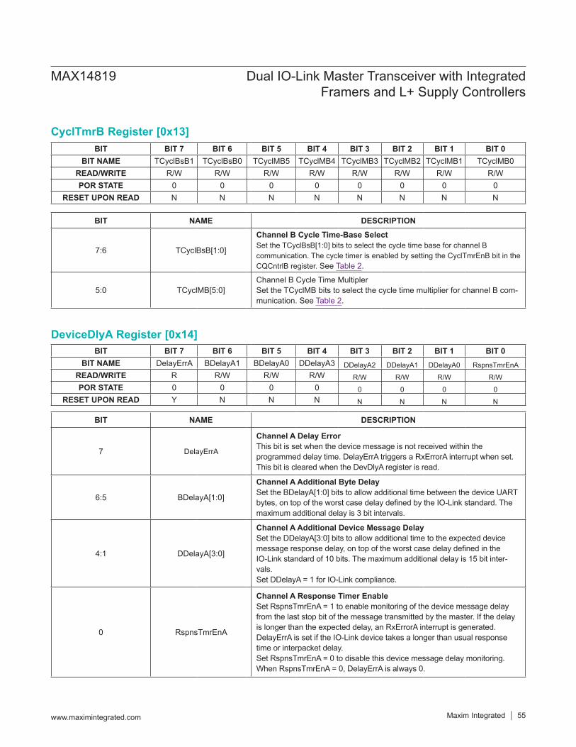
CyclTmrB Register [0x13]
DeviceDlyA Register [0x14]BIT BIT 7 BIT 6 BIT 5 BIT 4 BIT 3 BIT 2 BIT 1 BIT 0
BIT NAME DelayErrA BDelayA1 BDelayA0 DDelayA3 DDelayA2 DDelayA1 DDelayA0 RspnsTmrEnAREAD/WRITE R R/W R/W R/W R/W R/W R/W R/WPOR STATE 0 0 0 0 0 0 0 0
RESET UPON READ Y N N N N N N N
BIT NAME DESCRIPTION
7 DelayErrA
Channel A Delay ErrorThis bit is set when the device message is not received within the programmed delay time. DelayErrA triggers a RxErrorA interrupt when set. This bit is cleared when the DevDlyA register is read.
6:5 BDelayA[1:0]
Channel A Additional Byte Delay Set the BDelayA[1:0] bits to allow additional time between the device UART bytes,ontopoftheworstcasedelaydefinedbytheIO-Linkstandard.Themaximum additional delay is 3 bit intervals.
4:1 DDelayA[3:0]
Channel A Additional Device Message DelaySet the DDelayA[3:0] bits to allow additional time to the expected device messageresponsedelay,ontopoftheworstcasedelaydefinedinthe IO-Link standard of 10 bits. The maximum additional delay is 15 bit inter-vals.Set DDelayA = 1 for IO-Link compliance.
0 RspnsTmrEnA
Channel A Response Timer EnableSet RspnsTmrEnA = 1 to enable monitoring of the device message delay from the last stop bit of the message transmitted by the master. If the delay is longer than the expected delay, an RxErrorA interrupt is generated. DelayErrA is set if the IO-Link device takes a longer than usual response time or interpacket delay.Set RspnsTmrEnA = 0 to disable this device message delay monitoring. When RspnsTmrEnA = 0, DelayErrA is always 0.
BIT BIT 7 BIT 6 BIT 5 BIT 4 BIT 3 BIT 2 BIT 1 BIT 0BIT NAME TCyclBsB1 TCyclBsB0 TCyclMB5 TCyclMB4 TCyclMB3 TCyclMB2 TCyclMB1 TCyclMB0
READ/WRITE R/W R/W R/W R/W R/W R/W R/W R/WPOR STATE 0 0 0 0 0 0 0 0
RESET UPON READ N N N N N N N N
BIT NAME DESCRIPTION
7:6 TCyclBsB[1:0]
Channel B Cycle Time-Base SelectSet the TCyclBsB[1:0] bits to select the cycle time base for channel Bcommunication. The cycle timer is enabled by setting the CyclTmrEnB bit in the CQCntrlB register. See Table 2.
5:0 TCyclMB[5:0]Channel B Cycle Time MultiplerSet the TCyclMB bits to select the cycle time multiplier for channel B com-munication. See Table 2.
MAX14819 Dual IO-Link Master Transceiver with Integrated Framers and L+ Supply Controllers
www.maximintegrated.com Maxim Integrated 55
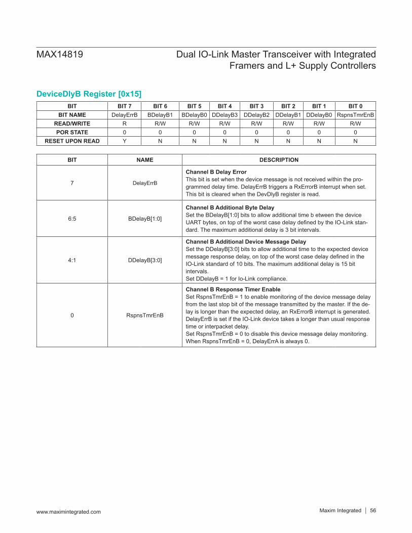
DeviceDlyB Register [0x15]BIT BIT 7 BIT 6 BIT 5 BIT 4 BIT 3 BIT 2 BIT 1 BIT 0
BIT NAME DelayErrB BDelayB1 BDelayB0 DDelayB3 DDelayB2 DDelayB1 DDelayB0 RspnsTmrEnBREAD/WRITE R R/W R/W R/W R/W R/W R/W R/WPOR STATE 0 0 0 0 0 0 0 0
RESET UPON READ Y N N N N N N N
BIT NAME DESCRIPTION
7 DelayErrB
Channel B Delay ErrorThis bit is set when the device message is not received within the pro-grammed delay time. DelayErrB triggers a RxErrorB interrupt when set. This bit is cleared when the DevDlyB register is read.
6:5 BDelayB[1:0]
Channel B Additional Byte Delay Set the BDelayB[1:0] bits to allow additional time b etween the device UARTbytes,ontopoftheworstcasedelaydefinedbytheIO-Linkstan-dard. The maximum additional delay is 3 bit intervals.
4:1 DDelayB[3:0]
Channel B Additional Device Message DelaySet the DDelayB[3:0] bits to allow additional time to the expected device messageresponsedelay,ontopoftheworstcasedelaydefinedintheIO-Link standard of 10 bits. The maximum additional delay is 15 bit intervals.Set DDelayB = 1 for Io-Link compliance.
0 RspnsTmrEnB
Channel B Response Timer EnableSet RspnsTmrEnB = 1 to enable monitoring of the device message delay from the last stop bit of the message transmitted by the master. If the de-lay is longer than the expected delay, an RxErrorB interrupt is generated. DelayErrB is set if the IO-Link device takes a longer than usual response time or interpacket delay.Set RspnsTmrEnB = 0 to disable this device message delay monitoring. When RspnsTmrEnB = 0, DelayErrA is always 0.
MAX14819 Dual IO-Link Master Transceiver with Integrated Framers and L+ Supply Controllers
www.maximintegrated.com Maxim Integrated 56
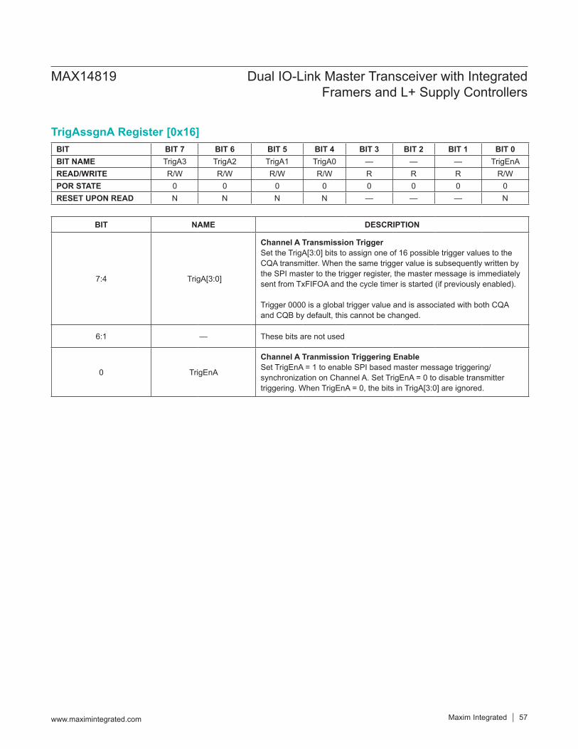
TrigAssgnA Register [0x16]BIT BIT 7 BIT 6 BIT 5 BIT 4 BIT 3 BIT 2 BIT 1 BIT 0BIT NAME TrigA3 TrigA2 TrigA1 TrigA0 — — — TrigEnAREAD/WRITE R/W R/W R/W R/W R R R R/WPOR STATE 0 0 0 0 0 0 0 0RESET UPON READ N N N N — — — N
BIT NAME DESCRIPTION
7:4 TrigA[3:0]
Channel A Transmission TriggerSet the TrigA[3:0] bits to assign one of 16 possible trigger values to the CQA transmitter. When the same trigger value is subsequently written by the SPI master to the trigger register, the master message is immediately sent from TxFIFOA and the cycle timer is started (if previously enabled).
Trigger 0000 is a global trigger value and is associated with both CQA and CQB by default, this cannot be changed.
6:1 — These bits are not used
0 TrigEnA
Channel A Tranmission Triggering EnableSet TrigEnA = 1 to enable SPI based master message triggering/ synchronization on Channel A. Set TrigEnA = 0 to disable transmitter triggering. When TrigEnA = 0, the bits in TrigA[3:0] are ignored.
MAX14819 Dual IO-Link Master Transceiver with Integrated Framers and L+ Supply Controllers
www.maximintegrated.com Maxim Integrated 57

TrigAssgnB Register [0x17]
L+CnfgA Register [0x18]
BIT BIT 7 BIT 6 BIT 5 BIT 4 BIT 3 BIT 2 BIT 1 BIT 0BIT NAME TrigB3 TrigB2 TrigB1 TrigB0 — — — TrigEnBREAD/WRITE R/W R/W R/W R/W R R R R/WPOR STATE 0 0 0 0 0 0 0 0RESET UPON READ N N N N — — — N
BIT NAME DESCRIPTION
7:4 TrigB[3:0]
Channel B Transmission TriggerSet the TrigB[3:0] bits to assign one of 16 possible trigger values to the CQB transmitter. When the same trigger value is subsequently written by the SPI master to the trigger register, the master message is immediately sent from TxFIFOB and the cycle timer is started (if previously enabled).
Trigger 0000 is a global trigger value and is associated with both CQA and CQB by default, this cannot be changed.
6:1 — These bits are not used.
0 TrigEnB
Channel B Tranmission Triggering EnableSet TrigEB = 1 to enable SPI based master message triggering/ synchronization on Channel B. Set TrigEnB = 0 to disable transmitter triggering. When TrigEnB = 0, the bits in TrigB[3:0] are ignored.
BIT BIT 7 BIT 6 BIT 5 BIT 4 BIT 3 BIT 2 BIT 1 BIT 0BIT NAME L+RTA1 L+RTA0 L+DynBLA L+BLA1 L+BLA0 L+CL2xA L+CLimDisA L+EnA
READ/WRITE R/W R/W R/W R/W R/W R/W R/W R/WPOR STATE 0 0 0 0 0 0 0 0
RESET UPON READ N N N N N N N N
BIT NAME DESCRIPTION
7:6 L+RTA[1:0]
Channel A L+ Sensor Supply Current-Limit Autoretry Period Set the L+RTA[1:0] bits to select the current-limit autoretry period: 00: Latchoff, no autoretry 01: 400ms 10: 4s 11: 12s
Latchoff is used for controller-managed timing.
MAX14819 Dual IO-Link Master Transceiver with Integrated Framers and L+ Supply Controllers
www.maximintegrated.com Maxim Integrated 58
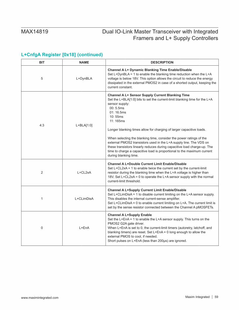
L+CnfgA Register [0x18] (continued)BIT NAME DESCRIPTION
5 L+DynBLA
Channel A L+ Dynamic Blanking Time Enable/DisableSet L+DynBLA = 1 to enable the blanking time reduction when the L+A voltage is below 18V. This option allows the circuit to reduce the energy dissipated in the external PMOS2 in case of a shorted output, keeping the current constant.
4:3 L+BLA[1:0]
Channel A L+ Sensor Supply Current Blanking TimeSet the L+BLA[1:0] bits to set the current-limit blanking time for the L+A sensor supply: 00: 5.5ms 01: 16.5ms 10: 55ms 11: 165ms
Longer blanking times allow for charging of larger capacitive loads.
When selecting the blanking time, consider the power ratings of the external PMOS2 transistors used in the L+A supply line. The VDS on these transistors linearly reduces during capacitive load charge-up. The time to charge a capacitive load is proportional to the maximum current during blanking time.
2 L+CL2xA
Channel A L+Double Current Limit Enable/DisableSet L+CL2xA = 1 to enable twice the current set by the current-limit resistor during the blanking time when the L+A voltage is higher than 18V. Set L+CL2xA = 0 to operate the L+A sensor supply with the normal current-limit threshold.
1 L+CLimDisA
Channel A L+Supply Current Limit Enable/Disable Set L+CLimDisA = 1 to disable current limiting on the L+A sensor supply. Thisdisablestheinternalcurrent-senseamplifier.Set L+CLimDisA = 0 to enable current limiting on L+A. The current limit is set by the sense resistor connected between the Channel A pMOSFETs.
0 L+EnA
Channel A L+Supply EnableSet the L+EnA = 1 to enable the L+A sensor supply. This turns on the PMOS2 G2A gate driver. When L+EnA is set to 0, the current-limit timers (autoretry, latchoff, and blanking timers) are reset. Set L+EnA = 0 long enough to allow the external PMOS to cool, if needed.ShortpulsesonL+EnA(lessthan200μs)areignored.
MAX14819 Dual IO-Link Master Transceiver with Integrated Framers and L+ Supply Controllers
www.maximintegrated.com Maxim Integrated 59
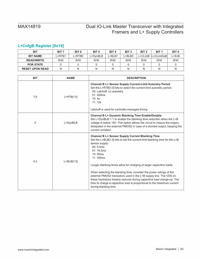
L+CnfgB Register [0x19]BIT BIT 7 BIT 6 BIT 5 BIT 4 BIT 3 BIT 2 BIT 1 BIT 0
BIT NAME L+RTB1 L+RTB0 L+DynBLB L+BLB1 L+BLB0 L+CL2xB L+CLimDisB L+EnBREAD/WRITE R/W R/W R/W R/W R/W R/W R/W R/WPOR STATE 0 0 0 0 0 0 0 0
RESET UPON READ N N N N N N N N
BIT NAME DESCRIPTION
7:6 L+RTB[1:0]
Channel B L+ Sensor Supply Current-Limit Autoretry PeriodSet the L+RTB[1:0] bits to select the current-limit autoretry period: 00: Latchoff, no autoretry 01: 400ms 10: 4s 11: 12s
Latchoff is used for controller-managed timing.
5 L+DynBLB
Channel B L+ Dynamic Blanking Time Enable/DisableSet L+DynBLB = 1 to enable the blanking time reduction when the L+B voltage is below 18V. This option allows the circuit to reduce the engery dissipated in the external PMOS2 in case of a shorted output, keeping the current constant.
4:3 L+BLB[1:0]
Channel B L+ Sensor Supply Current Blanking TimeSet the L+BLB[1:0] bits to set the current-limit blanking time for the L+B sensor supply: 00: 5.5ms 01: 16.5ms 10: 55ms 11: 165ms
Longer blanking times allow for charging of larger capacitive loads.
When selecting the blanking time, consider the power ratings of the external PMOS2 transistors used in the L+B supply line. The VDS on these transistors linearly reduces during capacitive load charge-up. The time to charge a capacitive load is proportional to the maximum current during blanking time.
MAX14819 Dual IO-Link Master Transceiver with Integrated Framers and L+ Supply Controllers
www.maximintegrated.com Maxim Integrated 60
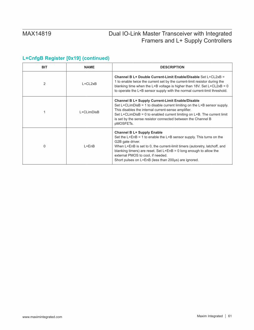
L+CnfgB Register [0x19] (continued)BIT NAME DESCRIPTION
2 L+CL2xB
Channel B L+ Double Current-Limit Enable/Disable Set L+CL2xB = 1 to enable twice the current set by the current-limit resistor during the blanking time when the L+B voltage is higher than 18V. Set L+CL2xB = 0 to operate the L+B sensor supply with the normal current-limit threshold.
1 L+CLimDisB
Channel B L+ Supply Current-Limit Enable/DisableSet L+CLimDisB = 1 to disable current limiting on the L+B sensor supply. Thisdisablestheinternalcurrent-senseamplifier.Set L+CLimDisB = 0 to enabled current limiting on L+B. The current limit is set by the sense resistor connected between the Channel B pMOSFETs.
0 L+EnB
Channel B L+ Supply EnableSet the L+EnB = 1 to enable the L+B sensor supply. This turns on the G2B gate driver. When L+EnB is set to 0, the current-limit timers (autoretry, latchoff, and blanking timers) are reset. Set L+EnB = 0 long enough to allow the external PMOS to cool, if needed.ShortpulsesonL+EnB(lessthan200μs)areignored.
MAX14819 Dual IO-Link Master Transceiver with Integrated Framers and L+ Supply Controllers
www.maximintegrated.com Maxim Integrated 61

IOStCfgA Register [0x1A]BIT BIT 7 BIT 6 BIT 5 BIT 4 BIT 3 BIT 2 BIT 1 BIT 0
BIT NAME DiLevelA CQLevelA TxEnA TxA DiFilterEnA DiEC3ThA DiCSourceA DiCsinkAREAD/WRITE R R R/W R/W R/W R/W R/W R/WPOR STATE 0 0 0 0 0 0 0 0
RESET UPON READ N N N N N N N N
BIT NAME DESCRIPTION
7 DiLevelA Channel A DIA Logic Level This bit is set when DIA = high. This bit is 0 when DIA = low.
6 CQLevelA Channel A CQA Logic Level This bit is set when CQA = high. This bit is 0 when CQA = low.
5 TxEnAChannel A CQ Transmitter Enable Input When TXTXENDis = 1, this bit has the same functionality as the TXENA input. When TXTXENDis = 0, this bit is ignored.
4 TxAChannel A CQ Transmitter Input When TXTXENDis = 1, this bit has the same functionality as the TXA input. When TXTXENDis = 0, this bit is ignored.
3 DiFilterEnA
Channel A DI Glitch Filter Enable/Disable SetDiFilterEnA=1toenabletheglitchfilteronDIA.SetDiFilterEnA=0todisabletheglitchfilter.Transientslongerthan1.3µs(typ)areignoredwhentheglitchfilterisenabled.
2 DiEC3ThAChannel A IEC61131-2 Type2/3 Threshold Select Set DiEC3ThA = 1 to enable type 2/3 thresholds on the DIA receiver. Set DiEC3ThA = 0 to enable type 1 threholds on the DIA receiver.
1 DiCSourceAChannel A DI Current Source Enable/DisableSet DiCSourceA = 1 to enable the 2mA (typ) current source on DIA. Set DiCSourceA = 0 to disable the current source.
0 DiCSinkAChannel A DI Current Sink EnableDisableSet DiCSinkA = 1 to enable the 2mA (typ) current sink on DIA. Set DiCSinkA = 0 to disable to current sink.
MAX14819 Dual IO-Link Master Transceiver with Integrated Framers and L+ Supply Controllers
www.maximintegrated.com Maxim Integrated 62
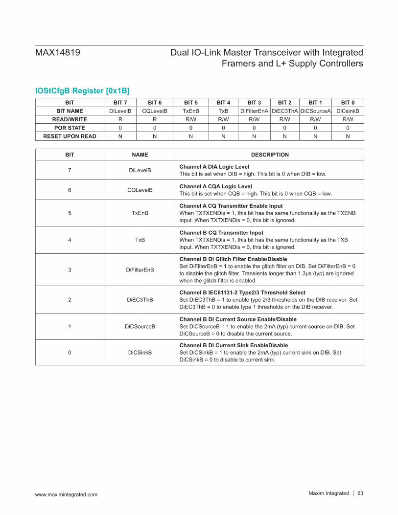
IOStCfgB Register [0x1B]BIT BIT 7 BIT 6 BIT 5 BIT 4 BIT 3 BIT 2 BIT 1 BIT 0
BIT NAME DiLevelB CQLevelB TxEnB TxB DiFilterEnA DiEC3ThA DiCSourceA DiCsinkBREAD/WRITE R R R/W R/W R/W R/W R/W R/WPOR STATE 0 0 0 0 0 0 0 0
RESET UPON READ N N N N N N N N
BIT NAME DESCRIPTION
7 DiLevelB Channel A DIA Logic Level This bit is set when DIB = high. This bit is 0 when DIB = low.
6 CQLevelB Channel A CQA Logic Level This bit is set when CQB = high. This bit is 0 when CQB = low.
5 TxEnBChannel A CQ Transmitter Enable Input When TXTXENDis = 1, this bit has the same functionality as the TXENB input. When TXTXENDis = 0, this bit is ignored.
4 TxBChannel B CQ Transmitter Input When TXTXENDis = 1, this bit has the same functionality as the TXB input. When TXTXENDis = 0, this bit is ignored.
3 DiFilterEnB
Channel B DI Glitch Filter Enable/Disable SetDiFilterEnB=1toenabletheglitchfilteronDIB.SetDiFilterEnB=0todisabletheglitchfilter.Transientslongerthan1.3µs(typ)areignoredwhentheglitchfilterisenabled.
2 DiEC3ThBChannel B IEC61131-2 Type2/3 Threshold Select Set DiEC3ThB = 1 to enable type 2/3 thresholds on the DIB receiver. Set DiEC3ThB = 0 to enable type 1 thresholds on the DIB receiver.
1 DiCSourceBChannel B DI Current Source Enable/DisableSet DiCSourceB = 1 to enable the 2mA (typ) current source on DIB. Set DiCSourceB = 0 to disable the current source.
0 DiCSinkBChannel B DI Current Sink EnableDisableSet DiCSinkB = 1 to enable the 2mA (typ) current sink on DIB. Set DiCSinkB = 0 to disable to current sink.
MAX14819 Dual IO-Link Master Transceiver with Integrated Framers and L+ Supply Controllers
www.maximintegrated.com Maxim Integrated 63

DrvrCurrLim Register [0x1C]Bit Bit 7 Bit 6 Bit 5 Bit 4 Bit 3 Bit 2 Bit 1 Bit 0Bit Name CL1 CL0 CLDis CLBL1 CLBL0 TAr1 TAr0 ArEnRead/Write R/W R/W R/W R/W R/W R/W R/W R/WPOR State 0 0 0 0 0 0 0 0Reset Upon Read N N N N N N N N
BIT NAME DESCRIPTION
7:6 CL[1:0]
CQA and CQB Driver Current-Limit SelectionSet the CL[1:0] bits to set the current limit for the CQA and CQB drivers when CLDis = 0: 00: 100mA 01: 200mA 10: 300mA 11: 500mA
5 CLDis
CQA and CQB Driver Current Enable/DisableSet CLDis = 1 to disable current limiting on the CQA and CQB drivers.Set CLDis = 0 to enable current limiting on the CQA and CQB driver. When CLDis = 0, the CQA and CQB driver current limit is set by the CL[1:0] bits.
4:3 CLBL[1:0]
Blanking Time SelectionSet the CLBL[1:0] bits to set the blanking time on the CQA and CQB drivers before a fault is indicated: 00:128μs01:500μs 10: 1ms 11: 5ms
The blanking time affects the maximum capacitive and incandescent lamp load that can be driven without triggering the fault signal. In order to drive very large capacitive or lamp loads, increase the blanking time and/or disable the autoretry timeout.
2:1 TAr[1:0]
Autoretry Timeout SelectionWhen a fault is detected on a driver output, the driver is disabled for the autoretry timeout. The driver is reenabled following the autoretry timeout. Set the TAr[1:0] bits to select the autoretry timeout: 00: 50ms 01: 100ms 10: 200ms 11: 500ms
0 ArEn
Autoretry Enable/DisableSet ArEn = 1 to enable autoretry functionality when a fault condition occurs on CQA or CQB. When a fault is detected on a driver, the driver is disabled fortheautoretryfixedofftime(setintheTAr[1:0]bits).Thedriveris reenabled and, following the blanking time, is rechecked. If the fault persists, the fault bit is left set and the driver is disabled again.When the fault is removed, the status bit is reset and the driver returns to normal operation.
MAX14819 Dual IO-Link Master Transceiver with Integrated Framers and L+ Supply Controllers
www.maximintegrated.com Maxim Integrated 64

Clock Register [0x1D]BIT BIT 7 BIT 6 BIT 5 BIT 4 BIT 3 BIT 2 BIT 1 BIT 0BIT NAME VCCWarnEn TXTXENDis — ClkOEn ClkDiv1 ClkDiv0 ExtClkEn XtalEnREAD/WRITE R/W R/W R R/W R/W R/W R/W R/WPOR STATE 0 0 0 0 0 0 0 0RESET UPON READ N N N N N N N N
BIT NAME DESCRIPTION
7 VCCWarnEn
VCC Warning Interrupt EnableSet VCCWarnEn = 1 to enable the StatusInt interrupt when VCC drops below the 18V (typ) VCC warning threshold. When VCCWarnEn = 0, the VCCWarn bit in the Status register is active, but does not generate a StatErrInt interrupt when the VCC voltage drops below 18V (typ).
6 TXTXENDis
CQ_ Pin Control Enable/DisableSet TXTXENDis = 1 to disable the external TX_ and TXEN_ input pins and to enable control of the CQ_ outputs through the Tx_ and TxEn_ bits in the IOStCfgA and IOStCfgB registers.
5 — This bit is not used.
4 ClkOEn Clock Output Pin (CLKO) Enable/DisableSet ClkOEn = 1 to enable the 3.686MHz output clock on the CLKO pin.
3:2 ClkDiv[1:0]
External Crystal Frequency DividerSet the ClkDiv[1:0] bits to select the frequency divider quotient related to the external crystal frequency: 00: 14.745MHz 01: 7.373MHz 10 and 11: 3.686MHz
1 ExtClkEn
External Clock Input Enable/DisableSet ExtClkEn = 1 to enable clocking from the CLKI input. XtalEn must be set to 0 when ExtClkEn is 1. Set ExtClkEn = 0 and XtalEn = 0 when the internal framer and neither the external clock, nor external crystal, are not used.
0 XtalEn
Crystal Oscillator Enable/DisableSet XtalEn = 1 to enable the internal crystal oscillator. ExtClkEn must be set to 0 when XtalEn is 1.Set XtalEn = 0 and ExtClkEn = 0 when the internal framer and neither the external clock, nor external crystal, are not used.
MAX14819 Dual IO-Link Master Transceiver with Integrated Framers and L+ Supply Controllers
www.maximintegrated.com Maxim Integrated 65

Status Register [0x1E]BIT BIT 7 BIT 6 BIT 5 BIT 4 BIT 3 BIT 2 BIT 1 BIT 0
BIT NAME ThShdnCOR ThWarnCOR VCCUVCOR VCCWarnCOR ThShdn ThWarn VCCUV VCCWarnREAD/WRITE R R R R R R R RPOR STATE 0 0 0 0 0 0 0 0
RESET UPON READ Y Y Y Y N N N N
BIT NAME DESCRIPTION
7 ThShdnCOR
Clear-On-Read Thermal ShutdownClear-on-read version of the ThShdn bit. This bit is set only when the ThShdn bit transitions from 0 to 1. A StatusInt interrupt is generated when this bit is set.This bit is cleared when Status register is read.
6 ThWarnCOR
Clear-On-Read Die Temperature WarningClear-on-read version of the ThWarn bit. This bit is set only when the ThWarn bit transitions from 0 to 1. A StatusInt interrupt is generated when this bit is set.This bit is cleared when the Status register is read.
5 VCCUVCOR
Clear-On-Read VCC Undervoltage WarningClear-on-read version of the VCCUV bit. This bit is set only when the VCCUV bit transitions from 0 to 1. A StatusInt interrupt is generated when this bit is set.This bit is cleared when the Status register is read.
4 VCCWarnCOR
Clear-On-Read VCC Supply Voltage WarningClear-on-read version of the VCCWarn bit. This bit is set only when the VCCWarn bit transitions from 0 to 1. A StatusInt interrupt is generated when this bit is set, if enabled by setting the VccWarnEn bit.This bit is cleared when the Status register is read.
3 ThShdn
Thermal ShutdownThis bit is set when the die temperature reaches 150°C and the die enters thermal shutdown. This bit is cleared when the die temperature falls and the part is no longer in thermal shutdown.
2 ThWarn
Die Temperature Warning This bit is set when the die junction temperature exceeds the 135°C warning threshold. This bit is cleard when the die temperature falls below 120°C.
1 VCCUVVCC UndervoltageThis bit is set when the VCC voltage falls below 9V (typ). It is cleared when the VCC voltage rises above 9V (typ).
0 VCCWarnVCC Supply Voltage WarningThis bit is set when the VCC voltage falls below 18V (max). It is cleared when the VCC voltage rises above 18V (max).
MAX14819 Dual IO-Link Master Transceiver with Integrated Framers and L+ Supply Controllers
www.maximintegrated.com Maxim Integrated 66

The MAX14819 continues to operate normally unless the die temperature reaches the +160°C (typ) thermal- shutdown threshold, at which time the device enters thermal shutdown.
Applications InformationThe Microcontroller InterfaceLogic-Level I/OsThe logic levels of the microcontroller interface I/Os are defined by VL. Apply a supply voltage between 1.62V and 5.5V to VL for normal operation. Logic outputs are supplied by VL.
Efficient Microcontroller Interface ManagementWhen the MAX14819 receives the device response message completely and error-free, an SPI RxDataRdy_ interrupt is generated and IRQ asserts. If enabled, the hardware interrupt (RXRDY_/LD1_) also asserts. When the SPI master receives the interrupt and then reads out the device message from the RxFIFO_, the RxDataRdy_ bit and RXRDY_/LD1_ pin interrupts are then automatically cleared.If the device message is received by the MAX14819 with errors or not in time, then an RxError_ interrupt occurs (IRQ asserts) and optionally, the RXERR_/LD2_ hard-ware interrupt also asserts if enabled. The MAX14819 can be configured to delete the device message under these circumstances and resend the master message with the SPI controller managing the process. The SPI controller is required only when the device message is ready and the MAX14819 is ready for the next master message (Figure 19).
RevID Register [0x1F]
Figure 19. IO-Link Cycle Timing
BIT BIT 7 BIT 6 BIT 5 BIT 4 BIT 3 BIT 2 BIT 1 BIT 0BIT NAME — — — — ID3 ID2 ID1 ID0
READ/WRITE R R R R R R R RPOR STATE 0 0 0 0 1 0 0 0
RESET UPON READ N N N N N N N N
BIT NAME DESCRIPTION
[7:4] — These bits are not used.
[3:0] ID[3:0]
CHIP ID Bits Thesebitsarereadyonly.TheyreflectthecurrentrevisionoftheMAX14819.The RevID register is meant for use during system/chip initialization and should not be used during IO-Link communication, since a byte may be lost in the RxFIFOA.
CYCLE TIMER
MASTER MESSAGE ON CQ_
DEVICE RESPONSE ON CQ_
TxFIFO RxFIFO TxFIFO
CONTROLLER SPI ACTIVITY
Write READ WRITE
START CYCLEN
START CYCLE (N+1)
RxDataRdy_INTERRUPT
MAX14819 Dual IO-Link Master Transceiver with Integrated Framers and L+ Supply Controllers
www.maximintegrated.com Maxim Integrated 67

Quartz Crystal SelectionThe crystal should have a frequency of either 3.6864MHz, 7.3728MHz, or 14.7456MHz. Select a crystal with an equivalent series resistance (ESR), including stray resis-tances,lessthan75Ω(max).The crystal oscillator drives the crystal with a power limited to70μW(max)powerdissipationinthecrystalbasedona14.7456MHz frequency, 8pF (max) shunt capacitance, and 75Ωequivalentseriesresistance.The input capacitance of the MAX14819 XIN and XOUT pins is 10pF, so no external capacitors are needed if the crystal’s load capacitance is in this range. If the selected crystal requires higher load capacitance, connect capaci-tors at XIN and XOUT to GND to make up for the difference.
Selecting the pMOS Transistors for the L+A/L+B SuppliesSelect PMOS1_ and PMOS2_ transistors whose drain-to-source current (IDS) carrying capability is higher than the maximum load current. The maximum load current for an application is set by the selected current limit and the L+CL2x_ bits. It is important to select pMOS FETs with low RDS(ON) to minimize the I2R heat generation in the module. When turned on, the PMOS1_ and PMOS2_ gate-to-source volt-age (VGS) is driven to -12.5V (typ). Use this bias condition for selecting the RDS(ON) of the pMOS. The pMOS transistors need to support the minimum and maximum voltages expected at the VCC and L+_ termi-nals. Select the transistor such that the drain-to-source voltage (VDS) of PMOS1_ FET is able to support the most negative VCC voltage, while the L+_ supply maintains a positive voltage (e.g., 28V) due to capacitance on the line. Similarly, ensure that the VDS of the PMOS2_ FET is large enough to support the maximum VCC voltage while L+_ is shorted to the most negative voltage.When the L+ supply output is shorted to ground or a negative voltage, the PMOS2_ FET dissipates the maxi-mum heat. The heat energy is determined by the current-limit current, the on-to-off duty cycle (i.e., blanking time/autoretry time), and the VDS voltage. Select a PMOS2_ transistor with a low thermal impedance to efficiently conduct away the heat.
Because the PMOS1_ transistor is not a part of the current-limiting circuitry, it does not dissipate as much heat as PMOS2_ during a short-circuit event.Ensure that the PMOS1_ and PMOS2_ FETs have gate-source threshold voltages less than 0.8V (VGS(th) < -0.8V). Examples of suitable pMOS FETs (depending on desired current limits) are SH8J31, NTTFS5116PL, and Si7415DN.
Transient ProtectionInductive LoadsBoth the CQ_ drivers and the L+_ supplies can drive and switch inductive loads. External TVS/zener-clamping diodes are required to clamp the kickback voltage and absorb energy when inductive loads are driven and fast turn-off is needed. The clamping voltage must be less than the Absolute Maximum voltage ratings of the CQA and CQB pins. In some cases, the EMC protection devices may be adequate for this purpose.
Surge, Burst, and ESD ProtectionThe CQ_, DI_, L+, and VCC pins need to be protected against electrostatic discharge (ESD), electrical fast tran-sients (EFT), and possible surges. The Absolute Maximum Ratings for these pins is (VCC - 70V) to +65V, providing significant headroom to allow the use of physically small protection diodes and higher protection voltages. For stan-dard ESD and burst protection demanded by the IO-Link specification, small package TVS (like the uClamp3603T or the SPT01-335) can be used to protect the CQ_, DI, and L+_ lines. If higher level surge ratings need to be achieved, suchas IEC61000-4-5 ±1kV/42Ω,SMAJ33A,or SMCJ48A, TVS protectors can be used on CQ_, DI_ and L+. 48V TVS diodes allow for high negative voltages, making these pins tolerant to negative short circuits and reverse polarity.For ±500V/2Ω IEC 61000-4-5 surge protection on theVCC input, Maxim recommends the SM30TY47AY and SM30TY33AY.
Using a Step-Down Regulator with the 5V Regulator To decrease power dissipation in the MAX14819, V5 can be powered by an external step-down regulator. Connect the external regulator’s output to the V5 input and disable the internal 5V regulator by connecting REGEN to ground (Figure 20).
MAX14819 Dual IO-Link Master Transceiver with Integrated Framers and L+ Supply Controllers
www.maximintegrated.com Maxim Integrated 68
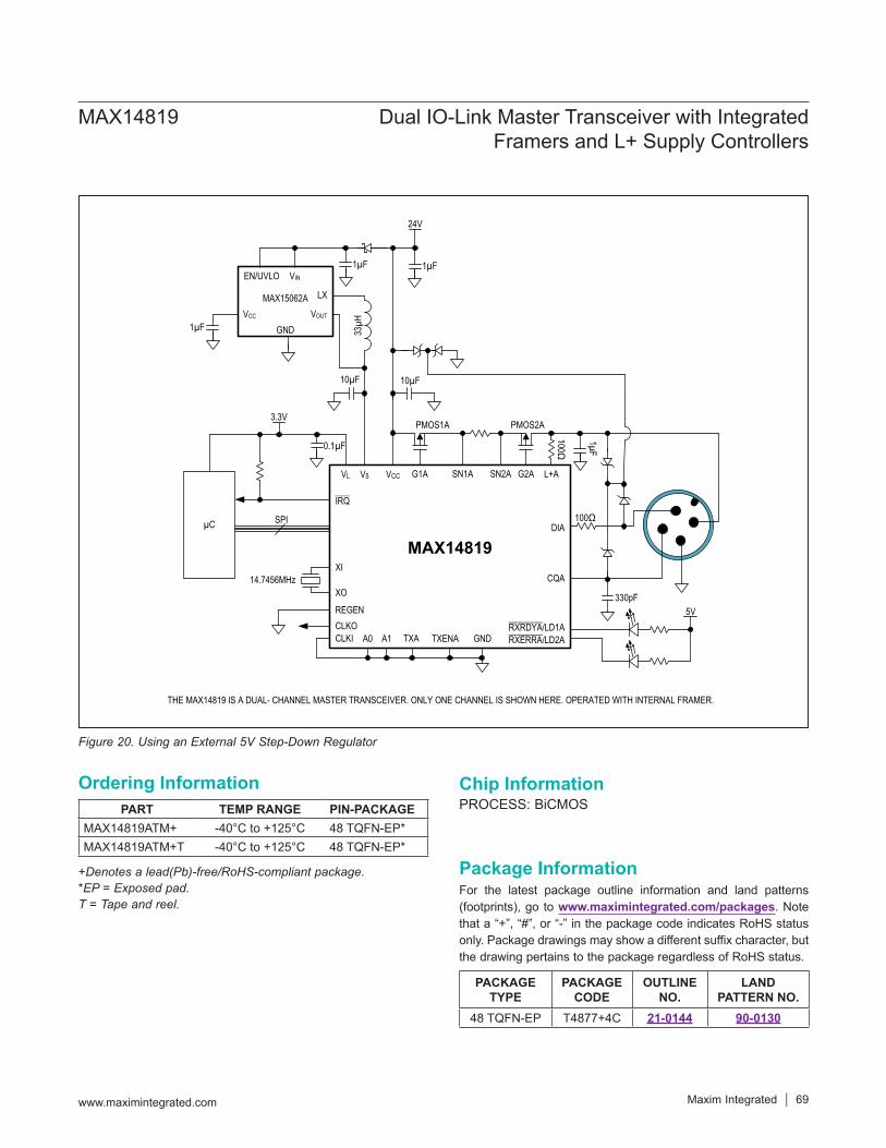
Figure 20. Using an External 5V Step-Down Regulator
+Denotes a lead(Pb)-free/RoHS-compliant package.*EP = Exposed pad.T = Tape and reel.
PART TEMP RANGE PIN-PACKAGEMAX14819ATM+ -40°C to +125°C 48 TQFN-EP*MAX14819ATM+T -40°C to +125°C 48 TQFN-EP*
PACKAGE TYPE
PACKAGE CODE
OUTLINE NO.
LAND PATTERN NO.
48 TQFN-EP T4877+4C 21-0144 90-0130
10µF
24V
0.1µF
1µF
VL V5 VCC G1A SN1A SN2A G2A L+A
330pF
IRQ
XI
XO
CLKOCLKI A0 A1 GND
MAX14819µC SPI
14.7456MHz CQA
DIA
3.3V
REGEN
TXA TXENA
THE MAX14819 IS A DUAL- CHANNEL MASTER TRANSCEIVER. ONLY ONE CHANNEL IS SHOWN HERE. OPERATED WITH INTERNAL FRAMER.
5V
RXRDYA/LD1ARXERRA/LD2A
VINEN/UVLO
VCC
LX
VOUT
10µF
GND 33µ
H
MAX15062A
PMOS1A PMOS2A
1µF 1µF
1µF100Ω
100Ω
MAX14819 Dual IO-Link Master Transceiver with Integrated Framers and L+ Supply Controllers
www.maximintegrated.com Maxim Integrated 69
Package InformationFor the latest package outline information and land patterns (footprints), go to www.maximintegrated.com/packages. Note that a “+”, “#”, or “-” in the package code indicates RoHS status only. Package drawings may show a different suffix character, but the drawing pertains to the package regardless of RoHS status.
Chip InformationPROCESS: BiCMOS
Ordering Information
REVISIONNUMBER
REVISIONDATE DESCRIPTION PAGES
CHANGED0 3/17 Initial release —
1 8/17 Updated/correctedfiguresandtext
1, 2, 8, 23, 26, 28, 39, 40, 45, 46, 52, 53, 62,
63, 69
Maxim Integrated cannot assume responsibility for use of any circuitry other than circuitry entirely embodied in a Maxim Integrated product. No circuit patent licenses are implied. Maxim Integrated reserves the right to change the circuitry and specifications without notice at any time. The parametric values (min and max limits) shown in the Electrical Characteristics table are guaranteed. Other parametric values quoted in this data sheet are provided for guidance.
Maxim Integrated and the Maxim Integrated logo are trademarks of Maxim Integrated Products, Inc.
MAX14819 Dual IO-Link Master Transceiver with Integrated Framers and L+ Supply Controllers
© 2017 Maxim Integrated Products, Inc. 70
Revision History
For pricing, delivery, and ordering information, please contact Maxim Direct at 1-888-629-4642, or visit Maxim Integrated’s website at www.maximintegrated.com.