A Low Mass On-chip Readout Scheme for Double-sided Silicon Strip Detectors
MAX14627/MAX14628Low-Power Headset Detectors with
SEND/END Button Support
Maxim Integrated Products 1
Typical Operating Circuits
19-6310; Rev 0; 5/12
Ordering Information appears at end of data sheet.
For related parts and recommended products to use with this part, refer to www.maxim-ic.com/MAX14627.related. Windows Mobile is a registered trademark of Microsoft Corporation.
Typical Operating Circuits continued at end of data sheet.
E V A L U A T I O N K I T A V A I L A B L E
General Description
The MAX14627/MAX14628 provide a simple solution for detecting the insertion and managing the operation of a 3.5mm stereo headset with a microphone. These devices integrate all circuitry needed to detect SEND/END button press events and generate required microphone bias volt-ages, and are fully compatible with Windows Mobile 7.The devices need only three GPIOs from the host control-ler to select between call mode and standby mode, and monitor the SEND/END and jack insertion status. In call mode, the low-noise LDO is enabled to provide DC bias to the externally preamplified microphone. In standby mode, microphone low-power pulsing is enabled to reduce sup-ply current while waiting for a SEND/END button press event. Two open-drain outputs signal the host controller when an insertion/removal or SEND/END button press event occurs. If a 3P headset without a microphone is inserted, the low-power pulsing can be disabled by setting the MODE input to high impedance.The MAX14627 operates from a 2.5V to 5.5V input voltage supply and features an internal 2.2V LDO output, while the MAX14628 operates from a 3.1V to 5.5V voltage supply and features an internal 2.8V LDO output voltage. Both devices control jack insertion detection by monitoring a 3.5mm socket with a normally open jack insertion switch. Additionally, the MAX14628 features open microphone detection.The MAX14627/MAX14628 are available in an 8-pin TDFN package, and are fully specified over the -40NC to +85NC extended temperature range.
Benefits and Features
S Versatile Jack Detection and Control MODE Three-State Microphone Bias Control MIC Switch Ground Detection (MAX14627) MIC Switch Open and Ground Detection (MAX14628)
S Compatible with Windows Mobile 7 and Google Android Microphone Button Press Detection
S High-Performance MIC Bias and Power Savings No Pop-Up Noises Ultra-Low Noise, High-PSRR MIC Bias Low-Power MIC Idle Mode Automatic Ultra-Low-Power Mode When Microphone Is Disabled
S PCB Space and Cost Savings Integrated ±15kV ESD Protection (HBM) on DETIN and MIC Input Terminals Small 8-Pin (2mm x 2mm) TDFN Package
Applications
Cell Phones
Portable Media Players
Tablet/Laptop PCs
SEND/END
MICROPHONE
1µF
MIC AUDIO DIRECTDRIVE
2.2kI
LEFT
MIC
DET
RIGHT
GND
1µF
VCC
1MI
VIO
1MI
VIO
SWD
MODE CAP
RES
MIC
DETINEP/GND
VCC
PROCESSOR
DET
MAX14628
For pricing, delivery, and ordering information, please contact Maxim Direct at 1-888-629-4642, or visit Maxim’s website at www.maxim-ic.com.

Maxim Integrated Products 2
MAX14627/MAX14628Low-Power Headset Detectors with
SEND/END Button Support
(Voltages referenced to GND.)VCC, MODE, SWD, DET ..........................................-0.3V to +6VCAP, MIC, RES ......................................... -0.3V to (VCC + 0.3V)DETIN .........................................................................-6V to +6VContinuous Current into Any Terminal ..........................Q100mAContinuous Power Dissipation (TA = +70NC) TDFN (derate 11.9mW/NC above +70NC) .................953.5mW
Operating Temperature Range .......................... -40NC to +85NCJunction Temperature .....................................................+150NCStorage Temperature Range ............................ -65NC to +150NCLead Temperature (soldering, 10s) ...............................+300NCSoldering Temperature (reflow) ......................................+260NC
TDFN Junction-to-Ambient Thermal Resistance (qJA) .......83.9°C/W Junction-to-Case Thermal Resistance (qJC) ...................37°C/W
ABSOLUTE MAXIMUM RATINGS
Note 1: Package thermal resistances were obtained using the method described in JEDEC specification JESD51-7, using a four-layer board. For detailed information on package thermal considerations, refer to www.maxim-ic.com/thermal-tutorial.
Stresses beyond those listed under “Absolute Maximum Ratings” may cause permanent damage to the device. These are stress ratings only, and functional opera-tion of the device at these or any other conditions beyond those indicated in the operational sections of the specifications is not implied. Exposure to absolute maximum rating conditions for extended periods may affect device reliability.
PACKAGE THERMAL CHARACTERISTICS (Note 1)
ELECTRICAL CHARACTERISTICS(VCC = 2.5V to 5.5V for MAX14627, VCC = 3.1V to 5.5V for MAX14628, CDETIN < 100pF, TA = -40NC to +85NC, unless otherwise noted. Typical values are at VCC = +3.6V, TA = +25NC.) (Note 2)
PARAMETER SYMBOL CONDITIONS MIN TYP MAX UNITS
DC CHARACTERISTICS
Supply Voltage Range VCCMAX14627 2.5 5.5
VMAX14628 3.1 5.5
VCC Undervoltage-Lockout Threshold
VCCUVLO VCC rising 0.9 1.7 2.45 V
VCC Supply Current ICC
MAX14627,VCC = 2.8V
MODE = low, DETIN = high
1.3
FA
MODE = low, DETIN = low, IMIC = 300FA
11.7
MODE = high, DETIN = low, IMIC = 300FA
800
MODE = high-Z, DETIN = low
6.0
MAX14628,VCC = 3.3V
MODE = low, DETIN = high
1.9
MODE = low, DETIN = low, IMIC = 300FA
13.2
MODE = high, DETIN = low, IMIC = 300FA
800
MODE = high-Z, DETIN = low
7.0

Maxim Integrated Products 3
MAX14627/MAX14628Low-Power Headset Detectors with
SEND/END Button SupportELECTRICAL CHARACTERISTICS (continued)(VCC = 2.5V to 5.5V for MAX14627, VCC = 3.1V to 5.5V for MAX14628, CDETIN < 100pF, TA = -40NC to +85NC, unless otherwise noted. Typical values are at VCC = +3.6V, TA = +25NC.) (Note 2)
PARAMETER SYMBOL CONDITIONS MIN TYP MAX UNITS
DETIN Pullup Resistance RDETIN 1000 kI
DETIN Series Resistance RDETININT 100 kI
Negative Current from DETIN INDETIN VDETIN = -2V 31 FA
MIC SEND/END Detection Threshold
VMICTH_LOW0.20 x VBIAS
0.22 x VBIAS
0.24 x VBIAS
V
MIC Open Switch Detection Threshold
VMICTH_HI MAX146280.90 x VBIAS
0.94 x VBIAS
0.98 x VBIAS
V
DETIN Detection Threshold VDETINTH Falling edge1/3 x VCC
1/2 x VCC
2/3 x VCC
V
MODE Pullup Resistance for High-Z Detection
RMODE_HI 200 kI
MODE Pulldown Resistance for High-Z Detection
RMODE_LO 200 kI
LINEAR REGULATOR (CAP)
Output Current Limit ICAP VCAP = 0V 4 mA
LDO Output Voltage VLDOMAX14627, VCC = 2.8V 2.0 2.2 2.45
VMAX14628, VCC = 3.3V 2.55 2.8 3.1
LDO PSRR PSRRLDO
Noise from VCC to CAP, f = 217Hz,VCC = 2.8V ±0.1V, ICAP = 300FA, MODE = high
100 dB
LDO Noise NLDOVCC = 2.8V, IMIC = 300FA, f = 100Hz to 4000Hz
11 FVRMS
LDO Turn-Off Time tLDO_OFF
MAX14627, VCC = 2.8V, RL = 2kI,VCAP from 90% to 10%
60
FsMAX14628, VCC = 3.3V, RL = 2kI,VCAP from 90% to 10%
60
Minimum Bypass Capacitance COUT (Note 3) 0.22 FF
DIGITAL SIGNALS (MODE, SWD, DET)
Input Logic-High Voltage VIH 1.4 V
Input Logic-Low Voltage VIL 0.4 V
MODE Average Current IMODE_LOW
Pulsing with 1/64 duty cycle from MODE terminal when MODE = low, DETIN = low (Note 4)
1 FA
MODE Input Resistance RMODE_HI When MODE = high, DETIN = low 120 220 380 kI
MODE External Maximum Leakage
IMODE_LKG When MODE = high-Z (Note 3) -1 +1 FA
Output Logic-High Leakage Current (Open Drain)
IOH_LKG VOH = 5V 1 FA
Maxim Integrated Products 4
MAX14627/MAX14628Low-Power Headset Detectors with
SEND/END Button SupportELECTRICAL CHARACTERISTICS (continued)(VCC = 2.5V to 5.5V for MAX14627, VCC = 3.1V to 5.5V for MAX14628, CDETIN < 100pF, TA = -40NC to +85NC, unless otherwise noted. Typical values are at VCC = +3.6V, TA = +25NC.) (Note 2)
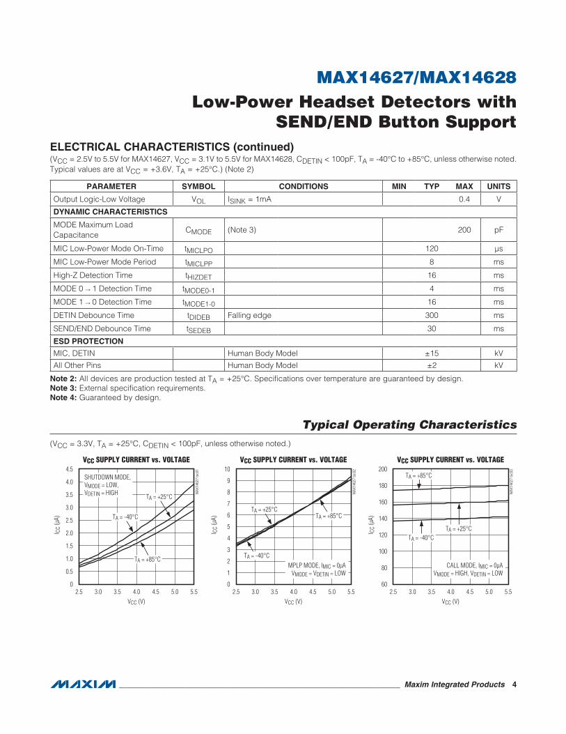
Typical Operating Characteristics(VCC = 3.3V, TA = +25NC, CDETIN < 100pF, unless otherwise noted.)
Note 2: All devices are production tested at TA = +25°C. Specifications over temperature are guaranteed by design.Note 3: External specification requirements.Note 4: Guaranteed by design.
PARAMETER SYMBOL CONDITIONS MIN TYP MAX UNITS
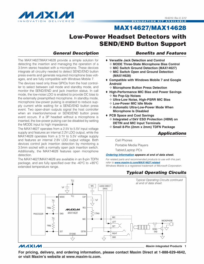
Output Logic-Low Voltage VOL ISINK = 1mA 0.4 V
DYNAMIC CHARACTERISTICS
MODE Maximum Load Capacitance
CMODE (Note 3) 200 pF
MIC Low-Power Mode On-Time tMICLPO 120 Fs
MIC Low-Power Mode Period tMICLPP 8 ms
High-Z Detection Time tHIZDET 16 ms
MODE 0 → 1 Detection Time tMODE0-1 4 ms
MODE 1 → 0 Detection Time tMODE1-0 16 ms
DETIN Debounce Time tDIDEB Falling edge 300 ms
SEND/END Debounce Time tSEDEB 30 ms
ESD PROTECTION
MIC, DETIN Human Body Model ±15 kV
All Other Pins Human Body Model ±2 kV
VCC SUPPLY CURRENT vs. VOLTAGE
MAX
1462
7 to
c01
VCC (V)
I CC
(µA)
5.04.54.03.53.0
0.5
1.0
1.5
2.0
2.5
3.0
3.5
4.0
4.5
02.5 5.5
TA = +85°C
TA = -40°C
TA = +25°C
SHUTDOWN MODE,VMODE = LOW, VDETIN = HIGH
1
2
3
4
5
6
7
8
9
VCC SUPPLY CURRENT vs. VOLTAGE
MAX
1462
7 to
c02
VCC (V)
I CC
(µA)
5.04.54.03.53.0
10
02.5 5.5
TA = +85°C
TA = -40°C
TA = +25°C
MPLP MODE, IMIC = 0µAVMODE = VDETIN = LOW
80
100
120
140
160
180
VCC SUPPLY CURRENT vs. VOLTAGE
MAX
1462
7 to
c03
VCC (V)
I CC
(µA)
5.04.54.03.53.0
200
602.5 5.5
CALL MODE, IMIC = 0µAVMODE = HIGH, VDETIN = LOW
TA = -40°CTA = +25°C
TA = +85°C

Maxim Integrated Products 5
MAX14627/MAX14628Low-Power Headset Detectors with
SEND/END Button SupportTypical Operating Characteristics (continued)
(VCC = 3.3V, TA = +25NC, CDETIN < 100pF, unless otherwise noted.)
2.1
2.2
2.3
2.4
MAX14627 CAP VOLTAGE vs. VCC
MAX
1462
7 to
c04
VCC (V)
V CAP
(V)
5.04.54.03.53.0
2.5
2.02.5 5.5
ICAP = 0mA
2.6
2.7
2.8
2.9
MAX14628 CAP VOLTAGE vs. VCC
MAX
1462
7 to
c05
VCC (V)V C
AP (V
)5.14.74.33.93.5
3.0
2.53.1 5.5
ICAP = 0mA
MAX14627 CAP VOLTAGE vs. CURRENT
MAX
1462
7 to
c06
ICAP (mA)
V CAP
(V)
654321
0.5
1.0
1.5
2.0
2.5
3.0
00 7
VCC = 3.3V
MAX14628 CAP VOLTAGE vs. CURRENT
MAX
1462
7 to
c07
ICAP (mA)
V CAP
(V)
654321
0.5
1.0
1.5
2.0
2.5
3.0
00 7
VCC = 3.3V
MAX14627 CAP VOLTAGEvs. TEMPERATURE
MAX
1462
7 to
c08
TA (°C)
V CAP
(V)
2.1
2.2
2.3
2.4
2.5
2.0-40 85603510-15
VCC = 3.3VICAP = 0mA
MAX14628 CAP VOLTAGEvs. TEMPERATURE
MAX
1462
7 to
c09
TA (°C)
V CAP
(V)
2.6
2.7
2.8
2.9
3.0
2.5-40 85603510-15
VCC = 3.3VICAP = 0mA
Maxim Integrated Products 6
MAX14627/MAX14628Low-Power Headset Detectors with
SEND/END Button SupportTypical Operating Characteristics (continued)
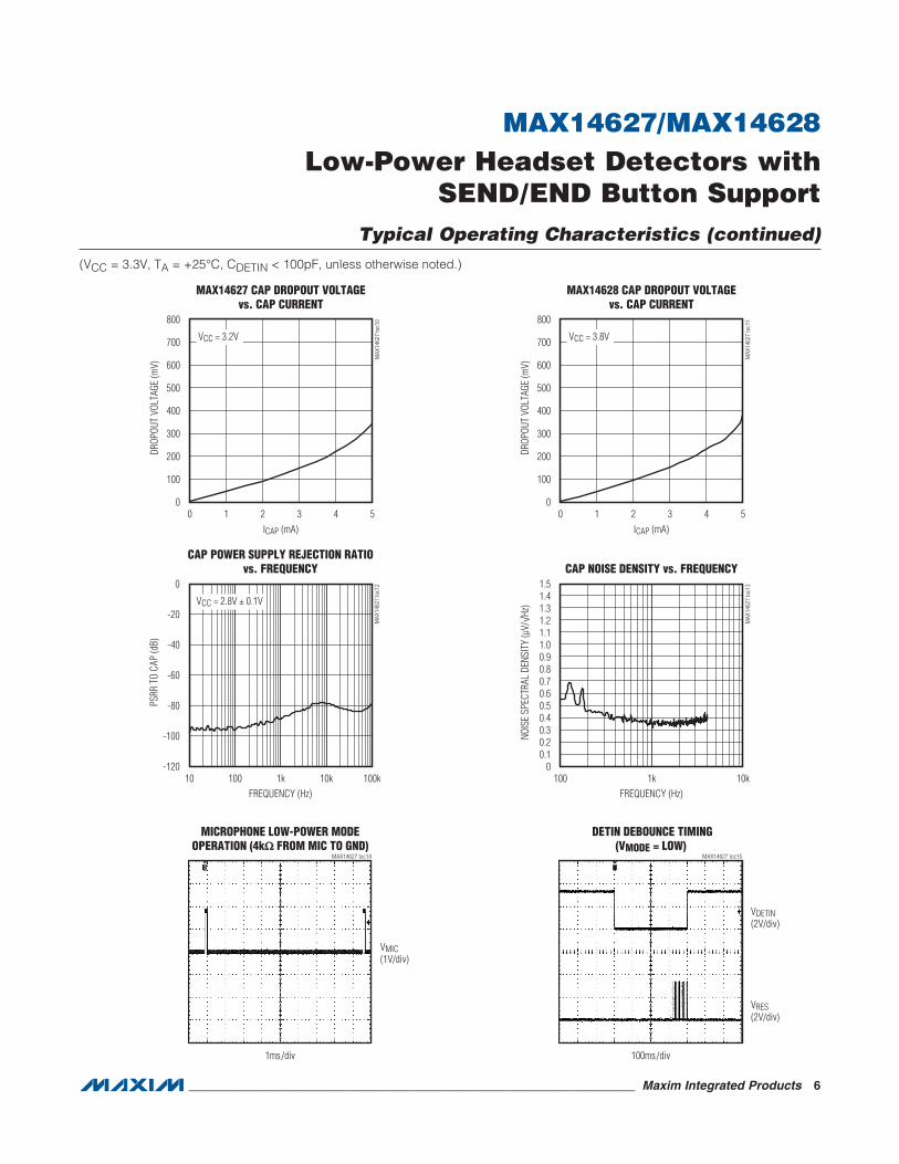
(VCC = 3.3V, TA = +25NC, CDETIN < 100pF, unless otherwise noted.)
MAX14627 CAP DROPOUT VOLTAGEvs. CAP CURRENT
MAX
1462
7 to
c10
DROP
OUT
VOLT
AGE
(mV)
100
200
300
400
500
600
700
800
0
ICAP (mA)
43210 5
VCC = 3.2V
MAX14628 CAP DROPOUT VOLTAGEvs. CAP CURRENT
MAX
1462
7 to
c11
DROP
OUT
VOLT
AGE
(mV)
100
200
300
400
500
600
700
800
0
ICAP (mA)
43210 5
VCC = 3.8V
CAP POWER SUPPLY REJECTION RATIOvs. FREQUENCY
MAX
1462
7 to
c12
FREQUENCY (Hz)
PSRR
TO
CAP
(dB)
10k1k100
-100
-80
-60
-40
-20
0
-12010 100k
VCC = 2.8V ± 0.1V
CAP NOISE DENSITY vs. FREQUENCY
MAX
1462
7 to
c13
FREQUENCY (Hz)
NOIS
E SP
ECTR
AL D
ENSI
TY (µ
V/√H
z)
1k
0.10.20.30.40.50.60.70.80.91.01.11.21.31.41.5
0100 10k
MICROPHONE LOW-POWER MODEOPERATION (4kI FROM MIC TO GND)
MAX14627 toc14
1ms/div
VMIC(1V/div)
DETIN DEBOUNCE TIMING(VMODE = LOW)
MAX14627 toc15
100ms/div
VRES(2V/div)
VDETIN(2V/div)

Maxim Integrated Products 7
MAX14627/MAX14628Low-Power Headset Detectors with
SEND/END Button SupportTypical Operating Characteristics (continued)
(VCC = 3.3V, TA = +25NC, CDETIN < 100pF, unless otherwise noted.)
SWD DEBOUNCE TIMING(MODE = L)
MAX14627 toc16
40ms/div
VMIC(2V/div)
VSWD(2V/div)
3.3V
3.3V
0V
0V
MIC vs. MODE(TRANSITIONS FROM HIGH TO HIGH-Z)
MAX14627 toc17
4ms/div
VMODE(1V/div)
VMIC(1V/div)
VDETIN = LOW,4kI FROM MIC TO GND
MIC vs. MODE(TRANSITIONS FROM LOW TO HIGH-Z)
MAX14627 toc18
4ms/div
VMODE(1V/div)
VMIC(1V/div)
VDETIN = LOW,4kI FROM MIC TO GND
MODE PULSING IN HIGH-Z(VDETIN = LOW)
MAX14627 toc19
2ms/div
VMODE(1V/div)
VCAP DISCHARGE TIMING MAX14627 toc20
40µs/div
VDETIN(1V/div)
VCAP(1V/div)

Maxim Integrated Products 8
MAX14627/MAX14628Low-Power Headset Detectors with
SEND/END Button Support
Pin Description
Pin Configuration
PIN NAME FUNCTION
1 RESResistor Connection. Connect an external 2.2kI resistor from RES to MIC for microphone biasing.
2 MODEMicrophone Mode Selection Three-State Input. MODE selects the operating mode. See the MODE Control Input section for more information.
3 SWD SEND/END Button Detection Output. SWD is an active-low, open-drain output.
4 DETJack Insertion Detection Output. DET is asserted when there is a 3.5mm jack inserted into the socket. DET is an active-low open-drain output.
5 CAPInternal LDO Output. Connect a 1FF ceramic (X5R, X7R, or better) capacitor between CAP and ground as close as possible to the device.
6 VCCSupply Voltage Input. Bypass VCC to ground with a 1FF ceramic capacitor as close as possible to the device.
7 DETINJack Insertion Detection Input. An internal comparator monitors DETIN for jack insertion/removal events.
8 MICMicrophone Connection Input. An internal comparator monitors MIC for SEND/END button press events.
— EP/GNDExposed Pad. The exposed pad is the ground connection for the device. Connect EP/GND to the ground plane.
1 3 4
+
8 6 5
MIC VCC CAP
MAX14627MAX14628
2
7
DENTIN
RES
*EP/GND
*CONNECT THE EXPOSED PAD (EP/GND) TO THE GROUND PLANE.
SWD DETMODE
TDFN
TOP VIEW
Maxim Integrated Products 9
MAX14627/MAX14628Low-Power Headset Detectors with
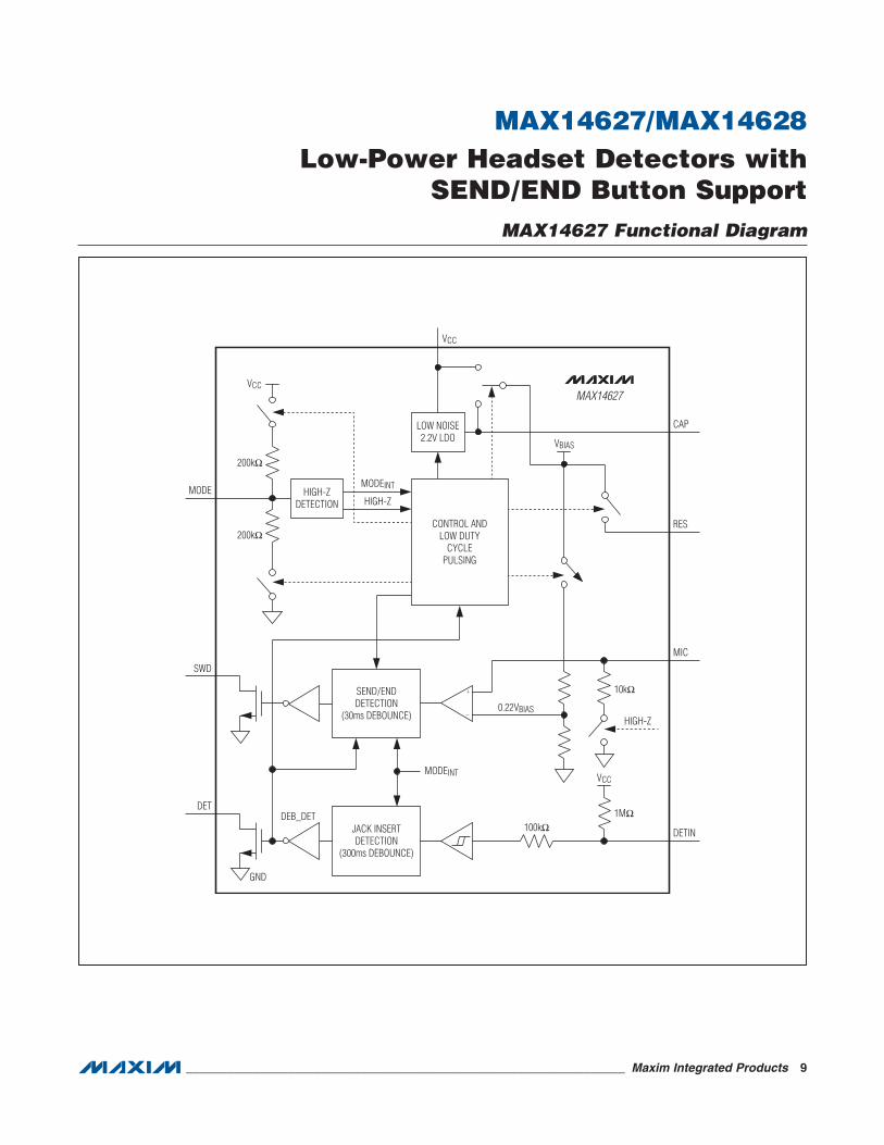
SEND/END Button SupportMAX14627 Functional Diagram
HIGH-ZDETECTION
200kI
MODE
CAP
RES
MIC
DETIN
SWD
DET
200kI
LOW NOISE2.2V LDO
VCC
VCC
VBIAS
HIGH-Z
HIGH-Z
MODEINT
CONTROL ANDLOW DUTY
CYCLEPULSING
SEND/ENDDETECTION
(30ms DEBOUNCE)
JACK INSERTDETECTION
(300ms DEBOUNCE)
100kI1MI
10kI
DEB_DET
MODEINT
0.22VBIAS
VCC
GND
MAX14627

Maxim Integrated Products 10
MAX14627/MAX14628Low-Power Headset Detectors with
SEND/END Button SupportMAX14628 Functional Diagram
HIGH-ZDETECTION
200kI
MODE
CAP
RES
MIC
DETIN
SWD
DET
200kI
LOW NOISE2.8V LDO
VCC
VCC
VBIAS
HIGH-Z
HIGH-Z
MODEINT
CONTROL ANDLOW DUTY
CYCLEPULSING
SEND/ENDDETECTION
(30ms DEBOUNCE)
JACK INSERTDETECTION
(300ms DEBOUNCE)
100kI 1MI
10kI
DEB_DET
MODEINT
VCC
GND
MAX14628
0.22VBIAS
0.94VBIAS

Maxim Integrated Products 11
MAX14627/MAX14628Low-Power Headset Detectors with
SEND/END Button SupportDetailed Description
The MAX14627/MAX14628 manage headsets by inte-grating 3.5mm jack insertion detection, microphone bias generation, and SEND/END button press detection. Both devices feature a low-power microphone mode to reduce the high bias current required for microphone operation while it is not in use. These devices require only a single three-state input (MODE) to select between call mode and two different low-power modes. See the Internal LDO Regulator and SEND/END Button Press Detection sections for details about the differences between these two devices.
Internal LDO RegulatorThe devices integrate a low-noise, low-dropout regulator (LDO) for biasing the microphone connected to MIC. The LDO output voltage is set at 2.2V for the MAX14627 and 2.8V for the MAX14628. The LDO is enabled and enters low-noise mode (LNM) when the MODE input is logic-high and a jack is detected (DETIN is low). Pull the MODE input low or leave it open to put the LDO in low-power shutdown mode (SDM).
Connect a 1FF capacitor from CAP to ground as close as possible to the pin.
Microphone Operation and Bias Voltage Generation
An externally preamplified microphone is connected to MIC. Connect MIC to RES through an external 2.2kI resistor to bias the microphone.
The devices generate a bias voltage (VBIAS) at RES. VBIAS is connected to the internal LDO when the LDO is on or connected to VCC when the LDO is off.
Microphone Low-Power Mode (MPLP)A microphone draws a large amount of current due to the 2.2kI required bias resistor when it is connected. This current is dissipated even when the microphone is not in use for audio input. This allows the SEND/END button detection to operate. The devices feature internal circuitry to reduce this current while simultaneously detecting SEND/END button press events.
When a jack is inserted (DETIN is low and DET is assert-ed low) and if MODE is pulled low, these devices enter the microphone low-power mode (MPLP). In this mode,
MIC is periodically connected to VBIAS (= VCC) through the 2.2kI resistor to RES only for a short duration (120Fs pulse over an 8ms period) to check for the SEND/END button press event (switch to GND in both MAX14627/MAX14628 and switch open in the MAX14628 only).
The devices exit MPLP when the MODE input transitions to logic-high or to high-Z state.Note that VBIAS is disconnected from RES when no jack is inserted and microphone low-power mode is not entered.
Jack Insertion DetectionThe devices monitor the DETIN input to detect jack inser-tion/removal events. Debounce circuitry ensures that transient voltages do not force the device to enter or exit microphone low-power mode due to false jack insertion/removal detection. DETIN input is capable of handling ±15kV HBM ESD event.
The devices are designed for sockets with a normally open pin. Without the 3.5mm jack inserted at DETIN, the input is pulled high by a large internal pullup resistor (1MI). When the jack is plugged in, DETIN is pulled to ground through the detection pin of the jack. DET is then asserted (after 300ms debounce time) and MIC is biased according to the logic state of the MODE input as follows:
• IfMODEis low, theexternal2.2kI resistor connects MIC to VCC in pulsing mode (MPLP) waiting for a SEND/END button press event.
• IfMODEishigh,theexternal2.2kI resistor connects MIC to LDO output continuously.
• IfMODEishigh-Z,MICisinternallypulleddown.
The devices feature an internal series 100kI resistor at DETIN and do not require a series resistor between DETIN and the jack even when a direct drive audio out-put is connected to DETIN through the detection pin of the jack. DETIN withstands input voltages down to -2V.
Ensure that the total capacitance on DETIN is less than 100pF.
SEND/END Button Press DetectionThe devices monitor the MIC input to detect SEND/END button press events. The SEND/END button press with the 4P microphone headset is detected and pulls the SWD output low if the voltage at MIC falls below the MIC switch to GND detection threshold (0.22 O VBIAS) for longer than 30ms.

Maxim Integrated Products 12
MAX14627/MAX14628Low-Power Headset Detectors with
SEND/END Button SupportThe MAX14628 also features an additional SEND/END detection mechanism through an additional MIC switch open detection threshold (0.94 O VBIAS). If there is an open switch, then MIC is pulled up to VBIAS in pulsing mode. If this happens for longer than 30ms, then the output SWD is pulled low.
The debounce period built into the SEND/END button press detection allows the mechanical SEND/END button to reach steady-state before applying the microphone bias. This mitigates click-and-pop noise.
The SEND/END detection circuitry is active whenever a jack is inserted (DETIN is low and DET is low).
MODE High-Z StateIf a 3P headset without a microphone is inserted, the SWD output is asserted low continuously. The user can turn off the microphone low-power mode by placing the MODE input to high-Z state after the recognition of a 3P jack. When in high-Z state, MODE is internally driven in pulsed mode.
MODE Control InputAn external host processor controls the MODE input. Table 1 shows the behavior of these devices based on the MODE input and jack insertion status. The device enters call mode when the MODE pin is logic-high and a jack is detected, enabling the LDO immediately in low-noise mode (LNM). The LDO output powers VBIAS and is connected to the microphone (MIC) through the external 2.2kI bias resistor.
Drive MODE low to put the devices in standby mode. In standby mode, VCC powers VBIAS, the LDO enters shut-down mode (SDM), and the microphone bias connection either turns off permanently if no jack is inserted or enters MPLP if a jack is inserted.
When MODE is set to high-Z, both the LDO and MPLP turn off. Also, the SWD output returns to a high-Z state, which can be used as a feedback of the device.
The MODE input is designed to be compatible with 1.8V logic when the VCC is up to 5.5V. The MODE pin must be properly controlled based on DETIN status to avoid the click-and-pop noise due to a headset insertion.
Applications Information
Typical Connections for 3.5mm JacksThere are two typical 3.5mm jacks: tip-ring-ring-sleeve (TRRS) with four conductors (Figure 1a) and tip-ring-sleeve (TRS) with three conductors (Figure 1b). The most common configuration of the TRRS jack is to use rings 1 and 2 for audio signals, ring 3 for ground, and ring 4 for a microphone. The TRS jack typically uses rings 1 and 2 for audio signals and rings 3 and 4 as ground.
Supported AccessoriesAll the devices support all standard configurations of headsets with a microphone and SEND/END button on a TRS or TRRS 3.5mm jack. Figure 2 shows the supported connections of the speakers, SEND/END button, and microphone to the jack.
Table 1. Operating Modes
*MIC is internally pulled down.
Figure 1. Typical 3.5mm Jacks
MODE LOW HIGH-Z HIGH
DETIN Low High Low High Low High
LDO Mode SDM SDM LNM SDM
MIC Bias Mode MPLP Off Off* Off 2.2kI Off
1 2
(a)
3 4
(b)
1 2 3 4

Maxim Integrated Products 13
MAX14627/MAX14628Low-Power Headset Detectors with
SEND/END Button SupportHeadset with No Microphone
When the 3.5mm jack in Figure 2a is inserted, the MIC input is pulled low permanently by the ground connection on the sleeve and the SWD output is logic-low perma-nently. This type of headset is supported by implement-ing a timeout period in software to recognize that the permanent SWD logic-low state is not due to a very long SEND/END button press event. In this case, the MODE input pin can be placed in high-Z state to disable the pulsing on the MIC pin (MPLP) and set the SWD output in high-Z state.
Headset with Microphone and Normally Open SEND/END Button in Parallel
When the 3.5mm jack in Figure 2b is inserted, the MIC input is pulled below the threshold only during a SEND/END button press event. The SWD output is logic-low when the SEND/END button is pressed for more than the 30ms (typ) debounce time.
Headset with Normally Open SEND/END Button and Resistive Remote Control
The devices support the 3.5mm jack with a microphone and two buttons in Figure 2c that is the standard Windows Mobile configuration. The threshold is set to detect a but-ton press, regardless of which button is pressed.
Headset with Microphone and Normally Closed SEND/END Button in Series
The MAX14628 supports the 3.5mm jack with a micro-phone and a normally closed series switch. When the switch opens for more than the 30ms (typ) debounce time (SEND/END button press event), the SWD output asserts low.
High-ESD ProtectionElectrostatic discharge (ESD)-protection structures are incorporated on all pins to protect against electrostatic discharges up to ±2kV Human Body Model (HBM) encountered during handling and assembly. DETIN and MIC are further protected against ESD up to ±15kV (HBM) without damage. After an ESD event, all the devices continue to function without latchup.
ESD Test ConditionsESD performance depends on a variety of conditions. Contact Maxim for a reliability report that documents test setup, test methodology, and test results. Figure 2. Supported 3.5mm Accessory Configurations
(a)
SPEAKER
1 2 3 4
SPEAKER
(b)
SPEAKER MICROPHONESEND/END
1 2 3 4
SPEAKER
(c)
SPEAKER MICROPHONE
1 2 3 4
SPEAKER
SEND/END
600Ω 200Ω
(d)
SPEAKERSEND/END
MICROPHONE
1 2 3 4
SPEAKER

Maxim Integrated Products 14
MAX14627/MAX14628Low-Power Headset Detectors with
SEND/END Button SupportTypical Operating Circuits (continued)
SEND/END
MICROPHONE
1µF
MIC AUDIO DIRECTDRIVE
2.2kI
LEFT
MIC
DET
RIGHT
GND
1µF
VCC
1MI
VIO
1MI
VIO
SWD
MODE CAP
RES
MIC
DETINEP/GND
VCC
PROCESSOR
DET
MAX14627

Maxim Integrated Products 15
MAX14627/MAX14628Low-Power Headset Detectors with
SEND/END Button SupportOrdering Information
+Denotes a lead(Pb)-free/RoHS-compliant package.T = Tape and reel.*EP = Exposed pad.
Package Information
For the latest package outline information and land patterns (footprints), go to www.maxim-ic.com/packages. Note that a “+”, “#”, or “-” in the package code indicates RoHS status only. Package drawings may show a different suffix character, but the drawing pertains to the package regardless of RoHS status.
Chip Information
PROCESS: BiCMOS
PART TEMP RANGE PIN-PACKAGE
MAX14627ETA+T -40NC to +85NC 8 TDFN-EP*
MAX14628ETA+T -40NC to +85NC 8 TDFN-EP*
PACKAGETYPE
PACKAGECODE
OUTLINENO.
LANDPATTERN NO.
8 TDFN-EP T822+2 21-0168 90-0065

Maxim cannot assume responsibility for use of any circuitry other than circuitry entirely embodied in a Maxim product. No circuit patent licenses are implied. Maxim reserves the right to change the circuitry and specifications without notice at any time. The parametric values (min and max limits) shown in the Electrical Characteristics table are guaranteed. Other parametric values quoted in this data sheet are provided for guidance.
Maxim Integrated Products, 120 San Gabriel Drive, Sunnyvale, CA 94086 408-737-7600 16
© 2012 Maxim Integrated Products Maxim is a registered trademark of Maxim Integrated Products, Inc.
MAX14627/MAX14628Low-Power Headset Detectors with
SEND/END Button SupportRevision History
REVISIONNUMBER
REVISIONDATE
DESCRIPTIONPAGES
CHANGED
0 5/12 Initial release —