MAX11214 24Bit 5mW 14B SNR 32ksps DeltaSigma … · • 2.6mA PGA Low-Noise Mode Current from AVDD...
53
General Description The MAX11214 is a 24-bit delta-sigma ADC that achieves excellent 140dB SNR while dissipating an ultra-low 5mW. Sample rates up to 32ksps allow both precision DC and AC measurements. Integral nonlinearity is guaranteed to 4ppm maximum. The THD is -122dB. The MAX11214 communicates via an SPI-compatible serial interface and is available in a small 24-pin TSSOP package. The MAX11214 offers a 6.5nV/√Hz noise programmable gain amplifier with gain settings between 1x to 128x. Optional buffers are also included to provide isolation of the signal inputs from the switched capacitor sampling network. This allows the MAX11214 to be used with high-impedance sources without compromising available dynamic range. The MAX11214 operates from a single 2.7V to 3.6V analog supply, or split ±1.8V analog supplies, allowing the analog input to be sampled below ground. The digital supply range is 2.0V to 3.6V, allowing communication with 2.5V, 3V, or 3.3V logic. Applications ● Seismic Data Acquisition ● Scientific Instrumentation ● High-Precision Portable Sensors ● Medical Equipment ● ATE Benefits and Features ● High Resolution for Instrumentation Applications that Require a Wide Dynamic Range • 134dB SNR at 15.6sps • 124dB SNR at 500sps • 21-Bit Noise-Free Resolution at 50sps • 18.6-Bit Noise-Free Resolution at 1ksps ● Longer Battery Life for Portable Applications • 1.2mA Operating Mode Current from AVDD • 2.6mA PGA Low-Noise Mode Current from AVDD • 1μA Sleep Current ● High Accuracy for DC Measurements • 1ppm INL (typ), 4ppm (max) ● Single or Split Analog Supplies Provide Input Voltage Range Flexibility • 2.7V to 3.6V (Single Supply) or ±1.8V (Split Supplies) ● Flexible High-Performance Filter Architecture Simplifies Design • Programmable SINC + FIR + IIR • Linear or Minimum Phase Response • Programmable Highpass Filter • Selectable FIR Data Rates: 62.5sps to 8ksps ● Enables System Integration • Low-Noise PGA with Gains of 1, 2, 4, 8, 16, 32, 64, 128 • Signal Buffer Optional • 3 General-Purpose I/Os ● Enables Integrated Part and System Calibration Capability for Gain and Offset ● Robust 24-Pin TSSOP Packaging Ordering Information and Functional Diagram appear at end of data sheet. 19-7569; Rev 0; 3/15 MAX11214 24-Bit, 5mW, 140dB SNR, 32ksps Delta-Sigma ADC with Integrated PGA EVALUATION KIT AVAILABLE
Transcript of MAX11214 24Bit 5mW 14B SNR 32ksps DeltaSigma … · • 2.6mA PGA Low-Noise Mode Current from AVDD...

General DescriptionThe MAX11214 is a 24-bit delta-sigma ADC that achieves excellent 140dB SNR while dissipating an ultra-low 5mW. Sample rates up to 32ksps allow both precision DC and AC measurements. Integral nonlinearity is guaranteed to 4ppm maximum. The THD is -122dB. The MAX11214 communicates via an SPI-compatible serial interface and is available in a small 24-pin TSSOP package.The MAX11214 offers a 6.5nV/√Hz noise programmable gain amplifier with gain settings between 1x to 128x. Optional buffers are also included to provide isolation of the signal inputs from the switched capacitor sampling network. This allows the MAX11214 to be used with high-impedance sources without compromising available dynamic range.The MAX11214 operates from a single 2.7V to 3.6V analog supply, or split ±1.8V analog supplies, allowing the analog input to be sampled below ground. The digital supply range is 2.0V to 3.6V, allowing communication with 2.5V, 3V, or 3.3V logic.
Applications ● Seismic Data Acquisition ● Scientific Instrumentation ● High-Precision Portable Sensors ● Medical Equipment ● ATE
Benefits and Features ● High Resolution for Instrumentation Applications that Require a Wide Dynamic Range
• 134dB SNR at 15.6sps• 124dB SNR at 500sps• 21-Bit Noise-Free Resolution at 50sps• 18.6-Bit Noise-Free Resolution at 1ksps
● Longer Battery Life for Portable Applications• 1.2mA Operating Mode Current from AVDD• 2.6mA PGA Low-Noise Mode Current from AVDD• 1μA Sleep Current
● High Accuracy for DC Measurements• 1ppm INL (typ), 4ppm (max)
● Single or Split Analog Supplies Provide Input Voltage Range Flexibility• 2.7V to 3.6V (Single Supply) or ±1.8V (Split Supplies)
● Flexible High-Performance Filter Architecture Simplifies Design• Programmable SINC + FIR + IIR• Linear or Minimum Phase Response• Programmable Highpass Filter• Selectable FIR Data Rates: 62.5sps to 8ksps
● Enables System Integration• Low-Noise PGA with Gains of 1, 2, 4, 8, 16,
32, 64, 128• Signal Buffer Optional• 3 General-Purpose I/Os
● Enables Integrated Part and System Calibration Capability for Gain and Offset
● Robust 24-Pin TSSOP PackagingOrdering Information and Functional Diagram appear at end of data sheet.
19-7569; Rev 0; 3/15
MAX11214 24-Bit, 5mW, 140dB SNR, 32ksps Delta-Sigma ADC with Integrated PGA
EVALUATION KIT AVAILABLE
MAX11214 24-Bit, 5mW, 140dB SNR, 32ksps Delta-Sigma ADC with Integrated PGA
www.maximintegrated.com Maxim Integrated │ 2
TABLE OF CONTENTS
General Description . . . . . . . . . . . . . . . . . . . . . . . . . . . . . . . . . . . . . . . . . . . . . . . . . . . . . . . . . . . . . . . . . . . . . . . . . . . . 1Applications . . . . . . . . . . . . . . . . . . . . . . . . . . . . . . . . . . . . . . . . . . . . . . . . . . . . . . . . . . . . . . . . . . . . . . . . . . . . . . . . . . 1Benefits and Features . . . . . . . . . . . . . . . . . . . . . . . . . . . . . . . . . . . . . . . . . . . . . . . . . . . . . . . . . . . . . . . . . . . . . . . . . . 1Absolute Maximum Ratings . . . . . . . . . . . . . . . . . . . . . . . . . . . . . . . . . . . . . . . . . . . . . . . . . . . . . . . . . . . . . . . . . . . . . . 6Package Thermal Characteristics . . . . . . . . . . . . . . . . . . . . . . . . . . . . . . . . . . . . . . . . . . . . . . . . . . . . . . . . . . . . . . . . . 6Electrical Characteristics . . . . . . . . . . . . . . . . . . . . . . . . . . . . . . . . . . . . . . . . . . . . . . . . . . . . . . . . . . . . . . . . . . . . . . . . 6Typical Operating Characteristics . . . . . . . . . . . . . . . . . . . . . . . . . . . . . . . . . . . . . . . . . . . . . . . . . . . . . . . . . . . . . . . . .11Pin Configuration . . . . . . . . . . . . . . . . . . . . . . . . . . . . . . . . . . . . . . . . . . . . . . . . . . . . . . . . . . . . . . . . . . . . . . . . . . . . . 15Pin Description . . . . . . . . . . . . . . . . . . . . . . . . . . . . . . . . . . . . . . . . . . . . . . . . . . . . . . . . . . . . . . . . . . . . . . . . . . . . . . . 15Functional Diagram . . . . . . . . . . . . . . . . . . . . . . . . . . . . . . . . . . . . . . . . . . . . . . . . . . . . . . . . . . . . . . . . . . . . . . . . . . . 17Detailed Description. . . . . . . . . . . . . . . . . . . . . . . . . . . . . . . . . . . . . . . . . . . . . . . . . . . . . . . . . . . . . . . . . . . . . . . . . . . 18
System Clock . . . . . . . . . . . . . . . . . . . . . . . . . . . . . . . . . . . . . . . . . . . . . . . . . . . . . . . . . . . . . . . . . . . . . . . . . . . . . . 18Voltage Reference Inputs . . . . . . . . . . . . . . . . . . . . . . . . . . . . . . . . . . . . . . . . . . . . . . . . . . . . . . . . . . . . . . . . . . . . . 18Analog Inputs . . . . . . . . . . . . . . . . . . . . . . . . . . . . . . . . . . . . . . . . . . . . . . . . . . . . . . . . . . . . . . . . . . . . . . . . . . . . . . 18
Input Buffers. . . . . . . . . . . . . . . . . . . . . . . . . . . . . . . . . . . . . . . . . . . . . . . . . . . . . . . . . . . . . . . . . . . . . . . . . . . . . 18Bypass/Direct Connect . . . . . . . . . . . . . . . . . . . . . . . . . . . . . . . . . . . . . . . . . . . . . . . . . . . . . . . . . . . . . . . . . . . . 18
Programmable Gain Amplifier (PGA) . . . . . . . . . . . . . . . . . . . . . . . . . . . . . . . . . . . . . . . . . . . . . . . . . . . . . . . . . . . . 18Input Voltage Range . . . . . . . . . . . . . . . . . . . . . . . . . . . . . . . . . . . . . . . . . . . . . . . . . . . . . . . . . . . . . . . . . . . . . . . . . 19Noise Performance vs. Data Rate . . . . . . . . . . . . . . . . . . . . . . . . . . . . . . . . . . . . . . . . . . . . . . . . . . . . . . . . . . . . . . 19Power-On Reset . . . . . . . . . . . . . . . . . . . . . . . . . . . . . . . . . . . . . . . . . . . . . . . . . . . . . . . . . . . . . . . . . . . . . . . . . . . . 25Power-Down Modes . . . . . . . . . . . . . . . . . . . . . . . . . . . . . . . . . . . . . . . . . . . . . . . . . . . . . . . . . . . . . . . . . . . . . . . . . 25Digital Filters . . . . . . . . . . . . . . . . . . . . . . . . . . . . . . . . . . . . . . . . . . . . . . . . . . . . . . . . . . . . . . . . . . . . . . . . . . . . . . . 27SINC Filter. . . . . . . . . . . . . . . . . . . . . . . . . . . . . . . . . . . . . . . . . . . . . . . . . . . . . . . . . . . . . . . . . . . . . . . . . . . . . . . . . 27FIR Filter . . . . . . . . . . . . . . . . . . . . . . . . . . . . . . . . . . . . . . . . . . . . . . . . . . . . . . . . . . . . . . . . . . . . . . . . . . . . . . . . . . 27Highpass Filter . . . . . . . . . . . . . . . . . . . . . . . . . . . . . . . . . . . . . . . . . . . . . . . . . . . . . . . . . . . . . . . . . . . . . . . . . . . . . 30Serial Interface . . . . . . . . . . . . . . . . . . . . . . . . . . . . . . . . . . . . . . . . . . . . . . . . . . . . . . . . . . . . . . . . . . . . . . . . . . . . . 31
Chip Select (CSB) . . . . . . . . . . . . . . . . . . . . . . . . . . . . . . . . . . . . . . . . . . . . . . . . . . . . . . . . . . . . . . . . . . . . . . . . 31SCLK (Serial Clock) . . . . . . . . . . . . . . . . . . . . . . . . . . . . . . . . . . . . . . . . . . . . . . . . . . . . . . . . . . . . . . . . . . . . . . . 31DIN (Serial Data Input). . . . . . . . . . . . . . . . . . . . . . . . . . . . . . . . . . . . . . . . . . . . . . . . . . . . . . . . . . . . . . . . . . . . . 31DOUT (Serial Data Output) . . . . . . . . . . . . . . . . . . . . . . . . . . . . . . . . . . . . . . . . . . . . . . . . . . . . . . . . . . . . . . . . . 31Data Ready (RDYB). . . . . . . . . . . . . . . . . . . . . . . . . . . . . . . . . . . . . . . . . . . . . . . . . . . . . . . . . . . . . . . . . . . . . . . 31SPI Incomplete Write Command Termination . . . . . . . . . . . . . . . . . . . . . . . . . . . . . . . . . . . . . . . . . . . . . . . . . . . 32SPI Incomplete Read Command Termination . . . . . . . . . . . . . . . . . . . . . . . . . . . . . . . . . . . . . . . . . . . . . . . . . . . 32SPI Timing Characteristics . . . . . . . . . . . . . . . . . . . . . . . . . . . . . . . . . . . . . . . . . . . . . . . . . . . . . . . . . . . . . . . . . 32
Modes and Registers . . . . . . . . . . . . . . . . . . . . . . . . . . . . . . . . . . . . . . . . . . . . . . . . . . . . . . . . . . . . . . . . . . . . . . . . 35Conversion Mode (MODE = 0) . . . . . . . . . . . . . . . . . . . . . . . . . . . . . . . . . . . . . . . . . . . . . . . . . . . . . . . . . . . . . . . . . 35Register Access Mode (MODE = 1) . . . . . . . . . . . . . . . . . . . . . . . . . . . . . . . . . . . . . . . . . . . . . . . . . . . . . . . . . . . . . 35

MAX11214 24-Bit, 5mW, 140dB SNR, 32ksps Delta-Sigma ADC with Integrated PGA
www.maximintegrated.com Maxim Integrated │ 3
TABLE OF CONTENTS (continued)
Register Map . . . . . . . . . . . . . . . . . . . . . . . . . . . . . . . . . . . . . . . . . . . . . . . . . . . . . . . . . . . . . . . . . . . . . . . . . . . . . . . . 36Register Address Map. . . . . . . . . . . . . . . . . . . . . . . . . . . . . . . . . . . . . . . . . . . . . . . . . . . . . . . . . . . . . . . . . . . . . . . . 36Status Register (Read Only) . . . . . . . . . . . . . . . . . . . . . . . . . . . . . . . . . . . . . . . . . . . . . . . . . . . . . . . . . . . . . . . . . . . 37Control Registers . . . . . . . . . . . . . . . . . . . . . . . . . . . . . . . . . . . . . . . . . . . . . . . . . . . . . . . . . . . . . . . . . . . . . . . . . . . 39
Control 1 Register (Read/Write) . . . . . . . . . . . . . . . . . . . . . . . . . . . . . . . . . . . . . . . . . . . . . . . . . . . . . . . . . . . . . 39Control 2 Register (Read/Write) . . . . . . . . . . . . . . . . . . . . . . . . . . . . . . . . . . . . . . . . . . . . . . . . . . . . . . . . . . . . . 40Control 3 Register (Read/Write) . . . . . . . . . . . . . . . . . . . . . . . . . . . . . . . . . . . . . . . . . . . . . . . . . . . . . . . . . . . . . 41Control 4 Register (Read/Write) . . . . . . . . . . . . . . . . . . . . . . . . . . . . . . . . . . . . . . . . . . . . . . . . . . . . . . . . . . . . . 41Control 5 Register (Read/Write) . . . . . . . . . . . . . . . . . . . . . . . . . . . . . . . . . . . . . . . . . . . . . . . . . . . . . . . . . . . . . 42
Data Register (Read Only) . . . . . . . . . . . . . . . . . . . . . . . . . . . . . . . . . . . . . . . . . . . . . . . . . . . . . . . . . . . . . . . . . . . . 42Calibration . . . . . . . . . . . . . . . . . . . . . . . . . . . . . . . . . . . . . . . . . . . . . . . . . . . . . . . . . . . . . . . . . . . . . . . . . . . . . . . . . 43
Self-Calibration . . . . . . . . . . . . . . . . . . . . . . . . . . . . . . . . . . . . . . . . . . . . . . . . . . . . . . . . . . . . . . . . . . . . . . . . . . 43System Calibration. . . . . . . . . . . . . . . . . . . . . . . . . . . . . . . . . . . . . . . . . . . . . . . . . . . . . . . . . . . . . . . . . . . . . . . . 43SPI System Offset Calibration Register (SOC_SPI) . . . . . . . . . . . . . . . . . . . . . . . . . . . . . . . . . . . . . . . . . . . . . . 44ADC System Offset Calibration Register (SOC_ADC) . . . . . . . . . . . . . . . . . . . . . . . . . . . . . . . . . . . . . . . . . . . . 44SPI System Gain Calibration Register (SGC_SPI) . . . . . . . . . . . . . . . . . . . . . . . . . . . . . . . . . . . . . . . . . . . . . . . 44ADC System Gain Calibration Register (SGC_ADC) . . . . . . . . . . . . . . . . . . . . . . . . . . . . . . . . . . . . . . . . . . . . . 44SPI Self-Cal Offset Calibration Register (SCOC_SPI) . . . . . . . . . . . . . . . . . . . . . . . . . . . . . . . . . . . . . . . . . . . . 45ADC Self-Cal Offset Calibration Register (SCOC_ADC) . . . . . . . . . . . . . . . . . . . . . . . . . . . . . . . . . . . . . . . . . . 45SPI Self-Cal Gain Calibration Register (SCGC_SPI) . . . . . . . . . . . . . . . . . . . . . . . . . . . . . . . . . . . . . . . . . . . . . 45ADC Self-Cal Gain Calibration Register (SCGC_ADC) . . . . . . . . . . . . . . . . . . . . . . . . . . . . . . . . . . . . . . . . . . . 45Highpass Filter Configuration Register (Read/Write) . . . . . . . . . . . . . . . . . . . . . . . . . . . . . . . . . . . . . . . . . . . . . 47
GPIOs . . . . . . . . . . . . . . . . . . . . . . . . . . . . . . . . . . . . . . . . . . . . . . . . . . . . . . . . . . . . . . . . . . . . . . . . . . . . . . . . . . . . 47Conversion Synchronization Using SYNC Pin or SYNC_SPI Function . . . . . . . . . . . . . . . . . . . . . . . . . . . . . . . . . . 47
Continuous Mode. . . . . . . . . . . . . . . . . . . . . . . . . . . . . . . . . . . . . . . . . . . . . . . . . . . . . . . . . . . . . . . . . . . . . . . . . 47Modulator MODBITS Mode. . . . . . . . . . . . . . . . . . . . . . . . . . . . . . . . . . . . . . . . . . . . . . . . . . . . . . . . . . . . . . . . . . . . 48
Initializing MODBITS Mode . . . . . . . . . . . . . . . . . . . . . . . . . . . . . . . . . . . . . . . . . . . . . . . . . . . . . . . . . . . . . . . . . 48Exiting MODBITS Mode. . . . . . . . . . . . . . . . . . . . . . . . . . . . . . . . . . . . . . . . . . . . . . . . . . . . . . . . . . . . . . . . . . . . 48MODBITS Mode Pin Configurations . . . . . . . . . . . . . . . . . . . . . . . . . . . . . . . . . . . . . . . . . . . . . . . . . . . . . . . . . . 48DOUT/MB0. . . . . . . . . . . . . . . . . . . . . . . . . . . . . . . . . . . . . . . . . . . . . . . . . . . . . . . . . . . . . . . . . . . . . . . . . . . . . . 49GPIO3/MSYNC . . . . . . . . . . . . . . . . . . . . . . . . . . . . . . . . . . . . . . . . . . . . . . . . . . . . . . . . . . . . . . . . . . . . . . . . . . 49GPIO1/MB1 . . . . . . . . . . . . . . . . . . . . . . . . . . . . . . . . . . . . . . . . . . . . . . . . . . . . . . . . . . . . . . . . . . . . . . . . . . . . . 49RDYB/ICLK . . . . . . . . . . . . . . . . . . . . . . . . . . . . . . . . . . . . . . . . . . . . . . . . . . . . . . . . . . . . . . . . . . . . . . . . . . . . . 49
Typical Application Circuit . . . . . . . . . . . . . . . . . . . . . . . . . . . . . . . . . . . . . . . . . . . . . . . . . . . . . . . . . . . . . . . . . . . . . . 51Ordering Information . . . . . . . . . . . . . . . . . . . . . . . . . . . . . . . . . . . . . . . . . . . . . . . . . . . . . . . . . . . . . . . . . . . . . . . . . . 52Chip Information. . . . . . . . . . . . . . . . . . . . . . . . . . . . . . . . . . . . . . . . . . . . . . . . . . . . . . . . . . . . . . . . . . . . . . . . . . . . . . 52Package Information . . . . . . . . . . . . . . . . . . . . . . . . . . . . . . . . . . . . . . . . . . . . . . . . . . . . . . . . . . . . . . . . . . . . . . . . . . 52Revision History . . . . . . . . . . . . . . . . . . . . . . . . . . . . . . . . . . . . . . . . . . . . . . . . . . . . . . . . . . . . . . . . . . . . . . . . . . . . . . 53

MAX11214 24-Bit, 5mW, 140dB SNR, 32ksps Delta-Sigma ADC with Integrated PGA
www.maximintegrated.com Maxim Integrated │ 4
LIST OF FIGURESFigure 1. PGA Structure. . . . . . . . . . . . . . . . . . . . . . . . . . . . . . . . . . . . . . . . . . . . . . . . . . . . . . . . . . . . . . . . . . . . . . . . 19Figure 2. Usable Input and Output Common-Mode Range. . . . . . . . . . . . . . . . . . . . . . . . . . . . . . . . . . . . . . . . . . . . . 19Figure 3. Digital Filter Path . . . . . . . . . . . . . . . . . . . . . . . . . . . . . . . . . . . . . . . . . . . . . . . . . . . . . . . . . . . . . . . . . . . . . 27Figure 4a. SINC Magnitude Response . . . . . . . . . . . . . . . . . . . . . . . . . . . . . . . . . . . . . . . . . . . . . . . . . . . . . . . . . . . . 27Figure 4b. SINC Mag Response Zoomed-In . . . . . . . . . . . . . . . . . . . . . . . . . . . . . . . . . . . . . . . . . . . . . . . . . . . . . . . . 27Figure 5. Magnitude Response, Linear Phase FIR, 8ksps Data Rate. . . . . . . . . . . . . . . . . . . . . . . . . . . . . . . . . . . . . 28Figure 6. Magnitude Response, Minimum Phase FIR, 8ksps Data Rate . . . . . . . . . . . . . . . . . . . . . . . . . . . . . . . . . . 28Figure 7. Passband Ripple, Linear Phase FIR, 8ksps Data Rate . . . . . . . . . . . . . . . . . . . . . . . . . . . . . . . . . . . . . . . . 28Figure 8. Passband Ripple, Minimum Phase FIR, 8ksps Data Rate. . . . . . . . . . . . . . . . . . . . . . . . . . . . . . . . . . . . . . 28Figure 9. Phase Response, Linear Phase FIR, 8ksps Data Rate . . . . . . . . . . . . . . . . . . . . . . . . . . . . . . . . . . . . . . . . 29Figure 10. Step Response, Linear Phase FIR . . . . . . . . . . . . . . . . . . . . . . . . . . . . . . . . . . . . . . . . . . . . . . . . . . . . . . . 29Figure 11. Phase Response, Minimum Phase FIR, 8ksps Data Rate . . . . . . . . . . . . . . . . . . . . . . . . . . . . . . . . . . . . . 29Figure 12. Step Response, Minimum Phase FIR. . . . . . . . . . . . . . . . . . . . . . . . . . . . . . . . . . . . . . . . . . . . . . . . . . . . . 29Figure 13. DATA Ready Timing for All Conversion Modes . . . . . . . . . . . . . . . . . . . . . . . . . . . . . . . . . . . . . . . . . . . . . 31Figure 14. SPI Register Write Timing Diagram . . . . . . . . . . . . . . . . . . . . . . . . . . . . . . . . . . . . . . . . . . . . . . . . . . . . . . 32Figure 15. SPI Register Read Timing Diagram . . . . . . . . . . . . . . . . . . . . . . . . . . . . . . . . . . . . . . . . . . . . . . . . . . . . . . 33Figure 16. SPI Data Readout Timing Diagram . . . . . . . . . . . . . . . . . . . . . . . . . . . . . . . . . . . . . . . . . . . . . . . . . . . . . . 33Figure 17. SPI Command Byte Timing Diagram . . . . . . . . . . . . . . . . . . . . . . . . . . . . . . . . . . . . . . . . . . . . . . . . . . . . . 34Figure 18. Calibration Flow Diagram . . . . . . . . . . . . . . . . . . . . . . . . . . . . . . . . . . . . . . . . . . . . . . . . . . . . . . . . . . . . . . 46Figure 19. Synchronization Using Continuous Sync Mode Showing Relationship Between SYNC Pin and CLK Pin 47Figure 20. Synchronization Using Pulse Sync Mode Showing Relationship Between SYNC, RDYB, and CLK Pins 48Figure 21. Pin Configuration with MODBITS . . . . . . . . . . . . . . . . . . . . . . . . . . . . . . . . . . . . . . . . . . . . . . . . . . . . . . . . 48Figure 22. Timing Diagram for MODBITS Mode . . . . . . . . . . . . . . . . . . . . . . . . . . . . . . . . . . . . . . . . . . . . . . . . . . . . . 50

MAX11214 24-Bit, 5mW, 140dB SNR, 32ksps Delta-Sigma ADC with Integrated PGA
www.maximintegrated.com Maxim Integrated │ 5
LIST OF TABLESTable 1. Continuous Mode SNR vs Data Rate and PGA Gain with FIR Filter* . . . . . . . . . . . . . . . . . . . . . . . . . . . . . . . . . . . . . . . . . . . . . . . . . . . . . 20
Table 2. Continuous Mode Input Referred Noise (µVRMS) vs Data Rate and PGA Gain with FIR Filter* . . . . . . . . . . . . . . . . . 20
Table 3. Continuous Mode SNR (dB) vs Data Rate and PGA Gain with Sinc Filter*. . . . . . . . . . . . . . . . . . . . . . . . . . . . . . . . . . . . . . . . . . . . . . .21
Table 4. Continuous Mode Input-Referred Noise (µVRMS) vs. Data Rate and PGA Gain with Sinc Filter* . . . . . . . . . . . . . . . 22
Table 5. Single-Cycle Mode SNR (dB) vs. Data Rate and PGA Gain with Sinc Filter*. . . . . . . . . . . . . . . . . . . . . . . . 23Table 6. Single-Cycle Mode Input-Referred Noise (µVRMS) vs. Data Rate and PGA Gain with Sinc Filter* . . . . . . 24Table 7. MAX11214 Command Behavior from Pin (RSTB, SYNC) and SPI (RESET, SYNC_SPI) . . . . . . . . . . . . . . . . . . . 25Table 8. Max HPF[15:0] Register Values for Different Data Rates . . . . . . . . . . . . . . . . . . . . . . . . . . . . . . . . . . . . . . . 30Table 9. Examples of HPF[15:0] Register Values and Cutoff Frequencies . . . . . . . . . . . . . . . . . . . . . . . . . . . . . . . . . 30Table 10. Command Byte for Conversion Modes (MODE = 0) . . . . . . . . . . . . . . . . . . . . . . . . . . . . . . . . . . . . . . . . . . 35Table 11. Command Byte for Register Access Mode (MODE = 1) . . . . . . . . . . . . . . . . . . . . . . . . . . . . . . . . . . . . . . . 35Table 12. Register Address Map . . . . . . . . . . . . . . . . . . . . . . . . . . . . . . . . . . . . . . . . . . . . . . . . . . . . . . . . . . . . . . . . . 36Table 13. Programmable Conversion Rates . . . . . . . . . . . . . . . . . . . . . . . . . . . . . . . . . . . . . . . . . . . . . . . . . . . . . . . . 38Table 14. ADC Output Code Data Format . . . . . . . . . . . . . . . . . . . . . . . . . . . . . . . . . . . . . . . . . . . . . . . . . . . . . . . . . . 43Table 15. MODBITS Mode Pins . . . . . . . . . . . . . . . . . . . . . . . . . . . . . . . . . . . . . . . . . . . . . . . . . . . . . . . . . . . . . . . . . . 49

AVDD to AVSS .....................................................-0.3V to +3.9VDVDD to DGND ....................................................-0.3V to +3.9VDVDD to AVSS .....................................................-0.3V to +3.9VAVSS to DGND ..................................................-1.95V to +0.3VAnalog Inputs
(AINP, AINM, REFP, REFN, CAPP, CAPN) to AVSS ........... -0.3V to the lower of 3.9V or (VAVDD + 0.3V)
Digital Inputs to DGND (RSTB, SYNC, DIN, SCLK, CLK, GPIO1-3) ......... -0.3V to the lower of 3.9V or (VDVDD + 0.3V)
Digital Outputs to DGND (RDYB, DOUT, GPIO1-3) ......... -0.3V to the lower of 3.9V or (VDVDD + 0.3V)
Digital Inputs to AVSS (RSTB, SYNC, DIN, SCLK, CLK, GPIO1–GPIO3).................................................-0.3V to +3.9V
Digital Outputs to AVSS(RDYB, DOUT, GPIO1-3) .....................................-0.3V to +3.9VCAPREG to DGND ...............................................-0.3V to +2.2VCAPREG to AVSS ................................................-0.3V to +3.9VContinuous Power Dissipation (Single-Layer Board)
TSSOP (derate 13.9mW/°C above +70°C) .......... 1111.10mWOperating Temperature Range ........................... -40°C to +85°CStorage Temperature Range ............................ -55°C to +150°CJunction Temperature (continuous) .................................+150°CLead temperature (soldering, 10s) ..................................+300°CSoldering Temperature (reflow) .......................................+260°C
TSSOP Junction-to-Case Thermal Resistance(θJC).................13°C/W
Junction-to-Ambient Thermal Resistance (θJA)...........72°C/W
(Note 1)
Electrical Characteristics(VAVDD = 3.6V, VAVSS = 0V, VDVDD = 2.0V, VREFP = 2.5V, VREFN = 0V; fDATA = 1000sps, External Clock = fCLK = 4.096MHz; Continuous conversion mode (SCYCLE = 0); PGA maximum output is 300mV below AVDD and minimum output is 300mV above AVSS, TA = TMIN to TMAX, unless otherwise noted. Typical values are at TA = +25°C.) (Note 2)
PARAMETER SYMBOL CONDITIONS MIN TYP MAX UNITSSTATIC PERFORMANCE
Noise-Free Resolution (Note 3) NFR
50sps data rate, Bypass mode only 20.2 21Bits
1ksps data rate, Bypass mode only 18.0 18.6
NOISE REFERRED TO INPUT VN (See Tables 1–4)
Integral Nonlinearity INLBypass, Buffer, PGA = 1, 2 1 4
ppmPGA > 2 2
Offset Error VOS After system offset calibration 10 nV
Offset Drift VOS_DRIFT 50 nV/°C
Gain Error GERR After system gain calibration 2 ppm
Gain Drift GERR_DRIFT 0.05 ppm/°C
DC Common-Mode Rejection CMRDC
Bypass and Buffer mode 125 135dB
PGA Gain = 4 110 120
AVDD, AVSS DC Supply Rejection Ratio PSRRA
Bypass and Buffer mode 85 105dB
PGA Gain = 4 85 100
DVDD DC Supply Rejection Ratio PSRRD
Bypass and Buffer mode 110 120dB
PGA Gain = 4 105 120
MAX11214 24-Bit, 5mW, 140dB SNR, 32ksps Delta-Sigma ADC with Integrated PGA
www.maximintegrated.com Maxim Integrated │ 6
Note 1: Package thermal resistances were obtained using the method described in JEDEC specification JESD51-7, using a four-layer board. For detailed information on package thermal considerations, refer to www.maximintegrated.com/thermal-tutorial.
Absolute Maximum Ratings
Stresses beyond those listed under “Absolute Maximum Ratings” may cause permanent damage to the device. These are stress ratings only, and functional operation of the device at these or any other conditions beyond those indicated in the operational sections of the specifications is not implied. Exposure to absolute maximum rating conditions for extended periods may affect device reliability.
Package Thermal Characteristics

Electrical Characteristics (continued)(VAVDD = 3.6V, VAVSS = 0V, VDVDD = 2.0V, VREFP = 2.5V, VREFN = 0V; fDATA = 1000sps, External Clock = fCLK = 4.096MHz; Continuous conversion mode (SCYCLE = 0); PGA maximum output is 300mV below AVDD and minimum output is 300mV above AVSS, TA = TMIN to TMAX, unless otherwise noted. Typical values are at TA = +25°C.) (Note 2)
PARAMETER SYMBOL CONDITIONS MIN TYP MAX UNITSDYNAMIC PERFORMANCE
Signal-to-Noise Ratio (Notes 5 and 7) SNR
Bypass, Buffer (see Tables 1 to 6) 117 121dB
PGA Gain = 2 (see Tables 1 to 6) 116.4 120
Total Harmonic Distortion (fSIGNAL = 31.25Hz) THD
Bypass, Buffer -120 -116
dB
PGA = 1, 2 -122 -113
PGA = 4, 8, 16, 32 -120
PGA = 64 -118
PGA = 128 -115
Spurious-Free Dynamic Range (fSIGNAL = 31.25Hz) SFDR
Bypass, Buffer 122dB
PGA = 4 122ANALOG INPUTS/REFERENCE INPUTS
AIN Voltage Range VRNGUnipolar 0 VREF
VBipolar -VREF VREF
Absolute Input Voltage VABSRNG
Bypass mode VAVSS VAVDD
VPGA mode VAVSS
+ 0.3VAVDD - 1.3
Buffer mode VAVSS + 0.1
VAVDD - 0.1
AIN DC Input Leakage IINLEAK Sleep mode enabled -10 +10 nA
AIN Common-Mode Input Conductance GAINCM Bypass ±4 nA/V
AIN Common-Mode Input Current IAINCM
Buffer ±250 nA
PGA ±10 nA
AIN Differential Mode Input Conductance GAINDIFF Bypass ±11.5 µA/V
AIN Differential Mode Input Current IAINDIFF
Buffer ±10 nA
PGA ±0.15 nA
REF Differential Input Conductance GREFDIFF Active conversion state ±23.8 µA/V
REF Input Current at Power Down IREF_PD Sleep and Standby states ±100 nA
AIN Input Capacitance CIN Buffer disabled 3 pF
REF Input Capacitance CREF Buffer disabled 4.5 pF
Input and REF Sampling Rate fS 2.048 MHz
VREFP - VREFN Voltage Range
VRABSRNG (Note 6) VAVDD V
MAX11214 24-Bit, 5mW, 140dB SNR, 32ksps Delta-Sigma ADC with Integrated PGA
www.maximintegrated.com Maxim Integrated │ 7

Electrical Characteristics (continued)(VAVDD = 3.6V, VAVSS = 0V, VDVDD = 2.0V, VREFP = 2.5V, VREFN = 0V; fDATA = 1000sps, External Clock = fCLK = 4.096MHz; Continuous conversion mode (SCYCLE = 0); PGA maximum output is 300mV below AVDD and minimum output is 300mV above AVSS, TA = TMIN to TMAX, unless otherwise noted. Typical values are at TA = +25°C.) (Note 2)
PARAMETER SYMBOL CONDITIONS MIN TYP MAX UNITSREF Voltage Range VREF 2.0 VAVDD V
DIGITAL FILTER RESPONSE
SINC FILTERBandwidth (-3dB) BWSINC 0.203 fDATASettling Time (Latency) 5 1/fDATAFIR FILTERPassband Ripple -0.003 +0.003 dB
Passband (-0.01dB) 0.375 fDATABandwidth (-3dB) BWFIR 0.413 fDATAHighpass Filter Corner fHP 0.000375 0.1 fDATAStopband Attenuation 135 dB
Stopband fSTOP 0.5 fDATA
Group DelayMinimum phase filter 5
1/fDATALinear phase filter 31
Settling Time (Latency)Minimum phase filter 10
1/fDATALinear phase filter 62
LOGIC INPUTSInput Current ILEAK_DIG Leakage current only -1 +1 µA
Input Low Voltage VIL0.3x
VDVDDV
Input High Voltage VIH0.7x
VDVDDV
Input Hysteresis VHYS 200 mV
GPIO Input Low Voltage VIL_GPIO 0.4 V
GPIO Input High Voltage VIH_GPIO 1.0 V
GPIO Input Hysteresis VHYS_GPIO 20 mV
LOGIC OUTPUTSOutput Low Level VOL IOL = 1mA 0.4 V
Output High Level VOH IOH = 1mA 0.9x VDVDD
V
Floating State Leakage Current IDIGO_LEAK -10 +10 µA
Floating State Output Capacitance CDIGO 9 pF
MAX11214 24-Bit, 5mW, 140dB SNR, 32ksps Delta-Sigma ADC with Integrated PGA
www.maximintegrated.com Maxim Integrated │ 8

Electrical Characteristics (continued)(VAVDD = 3.6V, VAVSS = 0V, VDVDD = 2.0V, VREFP = 2.5V, VREFN = 0V; fDATA = 1000sps, External Clock = fCLK = 4.096MHz; Continuous conversion mode (SCYCLE = 0); PGA maximum output is 300mV below AVDD and minimum output is 300mV above AVSS, TA = TMIN to TMAX, unless otherwise noted. Typical values are at TA = +25°C.) (Note 2)
PARAMETER SYMBOL CONDITIONS MIN TYP MAX UNITSPOWER REQUIREMENTS
Analog Negative Supply VAVSS For split supplies, VAVSS = -VAVDD -1.8 0 V
Analog Positive Supply VAVDD For split supplies, VAVDD = -VAVSSVAVSS +
2.7VAVSS +
3.6 V
Digital Supply VDVDD 2.0 3.6 V
AVDD Sleep Current IAVDD_SLEEP 0.9 3 µA
AVDD Standby Current IAVDD_STBY 1.5 3 µA
DVDD Sleep Current IDVDD_SLEEP 0.25 1 µA
DVDD Standby Current IDVDD_STBY 21 200 µA
Analog Supply Current IAVDD
Bypass mode 1.2 1.6
mABuffers mode 1.4 1.7
PGA low-power mode 2.0 2.75
PGA low-noise mode 2.6 3.4
DVDD Operating Current
SINC filter 0.4 0.5
mAFIR filter, 1000sps 0.55 0.7
FIR filter, 8ksps 1.75 2.25
SPI TIMING REQUIREMENTS (See Figure 14–17)SCLK Frequency fSCLK 5 MHz
SCLK Clock Period tCP 200 ns
SCLK Pulse Width High tCH Allow 40% duty cycle 80 ns
SCLK Pulse Width Low tCL Allow 40% duty cycle 80 ns
CSB Low Setup tCSS0 CSB low to 1st SCLK rise setup 40 ns
CSB High Setup (Note 4) tCSS1
Required to prevent a 17th SCLK RE from being recognized by the device in a free-running application
40 ns
CSB Hold tCSH1SCLK falling edge to CSB rising edge, CSB hold time 3 ns
CSB Pulse Width tCSW Minimum CSB pulse width high 40 ns
DIN Setup tDS DIN setup to SCLK rising edge 40 ns
DIN Hold tDH DIN hold after SCLK rising edge 0 ns
DOUT Transition tDOT DOUT transition valid after SCLK fall 40 ns
MAX11214 24-Bit, 5mW, 140dB SNR, 32ksps Delta-Sigma ADC with Integrated PGA
www.maximintegrated.com Maxim Integrated │ 9

Electrical Characteristics (continued)(VAVDD = 3.6V, VAVSS = 0V, VDVDD = 2.0V, VREFP = 2.5V, VREFN = 0V; fDATA = 1000sps, External Clock = fCLK = 4.096MHz; Continuous conversion mode (SCYCLE = 0); PGA maximum output is 300mV below AVDD and minimum output is 300mV above AVSS, TA = TMIN to TMAX, unless otherwise noted. Typical values are at TA = +25°C.) (Note 2)
Note 2: Limits are 100% production tested at TA = +25°C. Limits over the operating temperature range are guaranteed by design and device characterization.
Note 3: Noise-free resolution is defined using the peak-to-peak input range and the peak-to-peak noise voltage. The peak-to-peak input range, VIN_RANGE_PP is defined as 2 x VREF. The peak-to-peak noise voltage is defined as the RMS noise voltage times 6.6. The NFR is calculated for bypass mode only and with SINC filter using the formula, NFR = log(VIN_RANGE_PP/(6.6 x VNOISE_RMS))/log(2).
Note 4: These specifications are not fully tested and are guaranteed by design and/or characterization.Note 5: Tested with input shorted (VAINP - VAINN = 0V). SNR = 20 x log10((VIN_RANGE)/(√2 x VNOISE_RMS)). SNR is calculated
for a 3.6V reference.Note 6: Reference common mode (VREFP + VREFN)/2 ≤ (VAVDD + VAVSS)/2 +0.1V.Note 7: Typical values tested with 150mV supply headroom.
PARAMETER SYMBOL CONDITIONS MIN TYP MAX UNITS
DOUT Hold tDOHOutput hold time remains valid after SCLK fall 3 ns
DOUT Disable tDODCSB rise to DOUT disable, CLOAD = 20pF 25 ns
CSB Fall to DOUT Valid tDOE
Default value of DOUT is ‘1’ for minimum specification, max specification for valid ‘0’ on RDYB
0 40 ns
SCLK Fall to RDYB ‘1’ tR1
RDYB transitions from ‘0’ to ‘1’ on falling edge of SCLK after LSB of DATA is shifted onto DOUT
0 40 ns
RSTB Fall or SYNC Rise to RDYB ‘1’ tR2
RDYB transitions from ‘0’ to ‘1’ on falling edge of RSTB or rising edge of SYNC after 2 fCLK cycles
2 1/fCLK
Minimum SYNC High Pulse Width tSYNC1 2 1/fCLK
Minimum RSTB Low Pulse Width tRSTB0 2 1/fCLK
MAX11214 24-Bit, 5mW, 140dB SNR, 32ksps Delta-Sigma ADC with Integrated PGA
www.maximintegrated.com Maxim Integrated │ 10

(VAVDD = 3.6V, VAVSS = 0V, VDVDD = 2.0V, VREFP = 2.5V, VREFN = 0V; fDATA = 1000sps, External Clock = fCLK = 4.096MHz; Continuous conversion mode (SCYCLE = 0); PGA maximum output is 300mV below AVDD and minimum output is 300mV above AVSS, TA = TMIN to TMAX, unless otherwise noted. Typical values are at TA = +25°C.)
-2.0
-1.5
-1.0
-0.5
0.0
0.5
1.0
1.5
2.0
-50 0 50 100 150
FREQ
UENC
Y VA
RIAT
ION
(%)
TEMPERATURE (°C)
INTERNAL OSCILLATORFREQUENCY VARIATION
vs. TEMPERATUREtoc04
0.00
0.20
0.40
0.60
0.80
1.00
1.20
1.40
1.60
-50 0 50 100 150
ACTI
VE C
URRE
NT (m
A)
TEMPERATURE (ºC)
ACTIVE CURRENTvs. TEMPERATURE toc01
Bypass Mode
FIR IDVDD_ACT
SINC IDVDD_ACT
IAVDD_ACT
1.00
10.00
100.00
1000.00
-50 0 50 100 150
STAN
DBY
CURR
ENT
(µA)
TEMPERATURE (°C)
IAVDD_STBY
STANDBY CURRENTvs. TEMPERATURE
toc02
IDVDD_STBY
0.00
0.20
0.40
0.60
0.80
1.00
1.20
1.40
1.60
1.80
-50 0 50 100 150
SLEE
P CU
RREN
T (µ
A)
TEMPERATURE (ºC)
SLEEP CURRENTvs. TEMPERATURE
toc03
IDVDD_SLEEP
IAVDD_SLEEP
-0.25
-0.20
-0.15
-0.10
-0.05
0.00
0.05
0.10
0.15
0.20
0.25
1.00 2.00 3.00 4.00 5.00
FREQ
UENC
Y VA
RIAT
ION
(%)
VDVDD (V)
INTERNAL OSCILLATORFREQUENCY VARIATION
vs. DVDD VOLTAGEtoc05
0
1
2
3
0 1 2 3 4
NOIS
E (µ
V RMS
)
COMMON-MODE VOLTAGE (V)
NOISE vs. COMMON-MODE VOLTAGEtoc06
BYPASS MODESINC FILTER
0.0
0.5
1.0
1.5
2.0
2.5
3.0
3.5
4.0
-50 0 50 100 150
NOIS
E (µ
V RMS
)
TEMPERATURE (°C)
NOISE vs. TEMPERATUREtoc07
BYPASS MODEFIR FILTER
0
200
400
600
800
1000
1200
1400
1600
1800
-10 -5 0 5 10
NUMB
ER O
F OC
CURR
ENCE
S
OUTPUT VOLTAGE (µV)
1ksps NOISE HISTOGRAMtoc08
Bypass ModeSINC FilterShorted Inputs
MAX11214 24-Bit, 5mW, 140dB SNR, 32ksps Delta-Sigma ADC with Integrated PGA
Maxim Integrated │ 11www.maximintegrated.com
Typical Operating Characteristics

(VAVDD = 3.6V, VAVSS = 0V, VDVDD = 2.0V, VREFP = 2.5V, VREFN = 0V; fDATA = 1000sps, External Clock = fCLK = 4.096MHz; Continuous conversion mode (SCYCLE = 0); PGA maximum output is 300mV below AVDD and minimum output is 300mV above AVSS, TA = TMIN to TMAX, unless otherwise noted. Typical values are at TA = +25°C.)
0
200
400
600
800
1000
1200
1400
1600
1800
-40 -20 0 20 40
NUMB
ER O
F OC
CURR
ENCE
S
OUTPUT VOLTAGE (µV)
32ksps NOISE HISTOGRAMtoc09
Bypass ModeSINC FilterShorted Inputs
-1
-0.8
-0.6
-0.4
-0.2
0
0.2
0.4
0.6
0.8
1
-2.5 -1.5 -0.5 0.5 1.5 2.5
INL (
ppm)
DIFFERENTIAL INPUT (V)
INL vs. INPUT VOLTAGE
+85°C
toc10A
+25°C
-40°C
Bypass Mode
-1
-0.8
-0.6
-0.4
-0.2
0
0.2
0.4
0.6
0.8
1
-2.5 -1.5 -0.5 0.5 1.5 2.5
INL (
ppm)
DIFFERNTIAL INPUT (V)
INL vs. INPUT VOLTAGE
+25°C
toc10B
BUFFER MODE
+85°C
-40°C
-1.5
-1
-0.5
0
0.5
1
1.5
-0.65 -0.325 0 0.325 0.65
INL (
ppm)
DIFFERENTIAL INPUT (V)
INL vs INPUT VOLTAGE
+85°C
toc10C
PGA = 4 LN Mode+25°C
-40°C
-1.5
-1
-0.5
0
0.5
1
1.5
-0.65 -0.325 0 0.325 0.65
INL (
ppm)
DIFFERNTIAL INPUT (V)
INL vs. INPUT VOLTAGE
+85°C
toc10D
PGA = 4 LP Mode
+25°C
-40°C
-15
-10
-5
0
5
10
-50 0 50 100 150
OFFS
ET E
RROR
(µV)
TEMPERATURE (ºC)
OFFSET ERRORvs. TEMPERATURE
toc11
CALIBRATED AT 25ºCBYPASS MODE
-6
-4
-2
0
2
4
6
8
2.5 3 3.5 4
OFFS
ET E
RROR
(µV)
VAVDD (V)
OFFSET ERRORvs. AVDD
toc12
CALIBRATED AT VAVDD = 3.15VBYPASS MODE
-30
-20
-10
0
10
20
30
40
50
1 2 3 4
OFFS
ET E
RROR
(µV)
VREFP - VREFN (V)
OFFSET ERRORvs. VREFP - VREFN toc13
CALIBRATED AT VREF = 2.5VBYPASS MODE
MAX11214 24-Bit, 5mW, 140dB SNR, 32ksps Delta-Sigma ADC with Integrated PGA
Maxim Integrated │ 12www.maximintegrated.com
Typical Operating Characteristics (continued)
(VAVDD = 3.6V, VAVSS = 0V, VDVDD = 2.0V, VREFP = 2.5V, VREFN = 0V; fDATA = 1000sps, External Clock = fCLK = 4.096MHz; Continuous conversion mode (SCYCLE = 0); PGA maximum output is 300mV below AVDD and minimum output is 300mV above AVSS, TA = TMIN to TMAX, unless otherwise noted. Typical values are at TA = +25°C.)
-180
-160
-140
-120
-100
-80
-60
-40
-20
0
0 100 200 300 400 500
AMPL
ITUD
E (d
B)
FREQUENCY (Hz)
OUTPUT SPECTRUMSHORTED INPUTS
BYPASS MODESINGLE CYCLE CONTINOUSSINC FILTER
toc14A
-180
-160
-140
-120
-100
-80
-60
-40
-20
0
0 100 200 300 400 500
AMPL
ITUD
E (d
B)
FREQUENCY (Hz)
OUTPUT SPECTRUMSHORTED INPUTS
toc14B
BYPASS MODECONTINOUS FIR FILTER
100
105
110
115
120
125
130
-50 0 50 100 150
SNR
(dB)
TEMPERATURE (°C)
SNRvs. TEMPERATURE
toc15
BYPASS MODEFIR FILTERFULL SCALE = ±3.6V
0
2
4
6
8
10
12
14
-15 -10 -5 0 5 10 15 20 25 30 35
NUMB
ER O
F OC
CURR
ENCE
S
OFFSET (nV)
OFFSET HISTOGRAM OF 147 PARTStoc16
BYPASS MODEAFTER CALIBRATONSHORTED INPUTS
0
5
10
15
20
25
30
35
-1.0 -0.6 -0.2 0.2 0.6 1.0 1.4 1.8
NUMB
ER O
F OC
CURR
ENCE
S
GAIN ERROR (ppm)
POSITIVE FULL-SCALEGAIN ERROR HISTOGRAM OF 147 PARTS
toc17A
BYPASS MODEAFTER CALIBRATION
0
5
10
15
20
25
30
-3.0 -2.2 -1.4 -0.6 0.2 1.0
NUMB
ER O
F OC
CURR
ENCE
S
GAIN ERROR (ppm)
NEGATIVE FULL-SCALEGAIN ERROR HISTOGRAM OF 147 PARTS
toc17B
BYPASS MODEAFTER CALIBRATION
-180
-160
-140
-120
-100
-80
-60
-40
-20
0
0 100 200 300 400 500
AMPL
ITUD
E (d
B)
FREQUENCY (Hz)
OUTPUT SPECTRUMtoc18A
8192 POINT FFTBYPASS MODETHD = -121.1dB
-180
-160
-140
-120
-100
-80
-60
-40
-20
0
0 100 200 300 400 500
AMPL
ITUD
E (d
B)
FREQUENCY (Hz)
OUTPUT SPECTRUMtoc18B
8192 POINT FFTBUFFER MODETHD = -119.5dB
MAX11214 24-Bit, 5mW, 140dB SNR, 32ksps Delta-Sigma ADC with Integrated PGA
Maxim Integrated │ 13www.maximintegrated.com
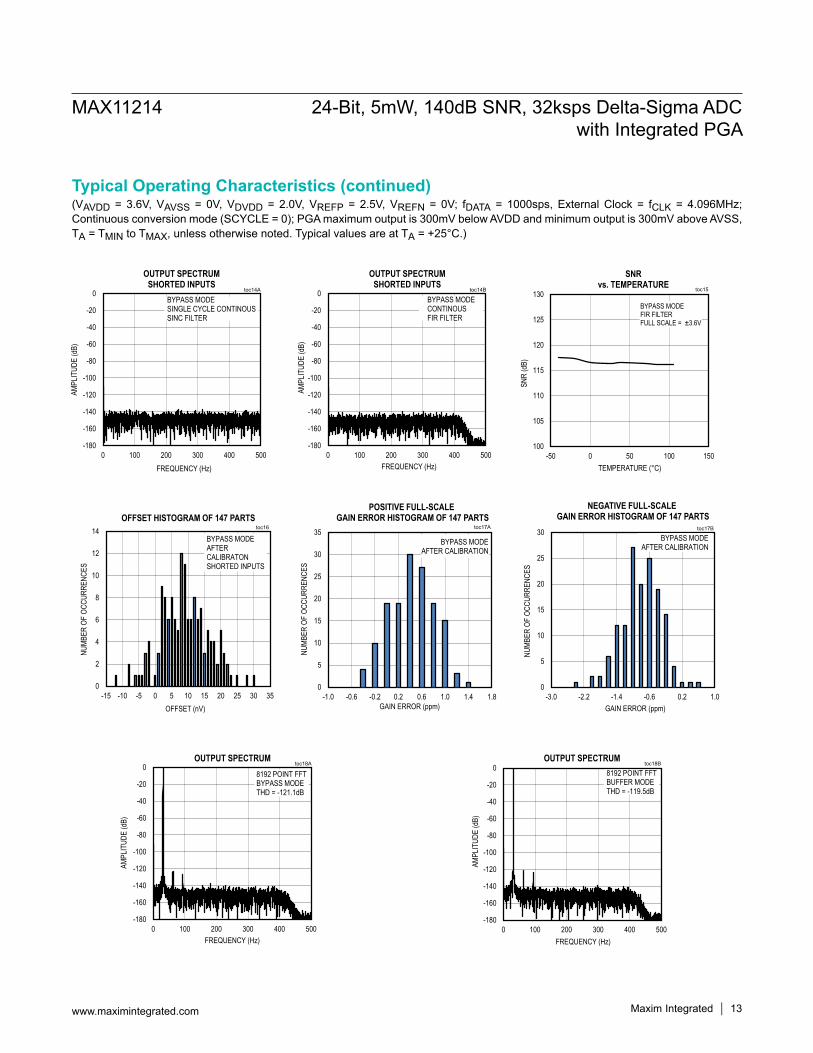
Typical Operating Characteristics (continued)

(VAVDD = 3.6V, VAVSS = 0V, VDVDD = 2.0V, VREFP = 2.5V, VREFN = 0V; fDATA = 1000sps, External Clock = fCLK = 4.096MHz; Continuous conversion mode (SCYCLE = 0); PGA maximum output is 300mV below AVDD and minimum output is 300mV above AVSS, TA = TMIN to TMAX, unless otherwise noted. Typical values are at TA = +25°C.)
-180
-160
-140
-120
-100
-80
-60
-40
-20
0
0 100 200 300 400 500
AMPL
ITUD
E (d
B)
FREQUENCY (Hz)
OUTPUT SPECTRUMtoc18C
8192 Point FFTPGA = 1 LN ModeTHD = -125.3dB
-180
-160
-140
-120
-100
-80
-60
-40
-20
0
0 100 200 300 400 500
AMPL
ITUD
E (d
B)
FREQUENCY (Hz)
OUTPUT SPECTRUMtoc18D
8192 Point FFTPGA = 1 LP ModeTHD = -124.0dB
-180
-160
-140
-120
-100
-80
-60
-40
-20
0
0 100 200 300 400 500
AMPL
ITUD
E (d
B)
FREQUENCY (Hz)
OUTPUT SPECTRUMtoc18E
8192 Point FFTPGA = 2 LN ModeTHD = -124.0dB
-180
-160
-140
-120
-100
-80
-60
-40
-20
0
0 100 200 300 400 500
AMPL
ITUD
E (d
B)
FREQUENCY (Hz)
OUTPUT SPECTRUMtoc18F
8192 Point FFTPGA=2 LP ModeTHD = -124.3dB
-180
-160
-140
-120
-100
-80
-60
-40
-20
0
0 100 200 300 400 500
AMPL
ITUD
E (d
B)
FREQUENCY (Hz)
OUTPUT SPECTRUMtoc18G
8192 Point FFTPGA = 4 LN ModeTHD = -120dB
-180
-160
-140
-120
-100
-80
-60
-40
-20
0
0 100 200 300 400 500
AMPL
ITUD
E (d
B)
FREQUENCY (Hz)
OUTPUT SPECTRUMtoc18H
8192 Point FFTPGA = 4 LP ModeTHD = -119dB
-0.2
0
0.2
0.4
0.6
0.8
1
1.2
1.4
1.6
1.8
-50 0 50 100 150
V REF
CURR
ENT
(nA)
TEMPERATURE (ºC)
VREF CURRENT vs. TEMPERATUREtoc19A
CALIBRATED AT 25ºC
STANDBY MODE SLEEP
MODE
58
59
60
61
-50 0 50 100 150
V REF
CURR
ENT
(nA)
TEMPERATURE (°C)
VREF CURRENT vs. TEMPERATUREtoc19B
CALIBRATED AT 25ºC
MAX11214 24-Bit, 5mW, 140dB SNR, 32ksps Delta-Sigma ADC with Integrated PGA
Maxim Integrated │ 14www.maximintegrated.com
Typical Operating Characteristics (continued)

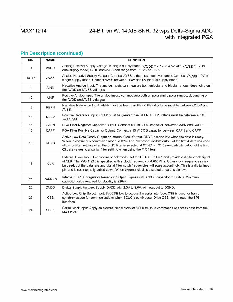
PIN NAME FUNCTION
1 DIN Serial Data Input. Data is clocked into DIN on the rising edge of SCLK. DIN configures the internal register writes or a command operation.
2 DOUT Serial Data Output or Real-Time Modulator MB0 Output. DOUT outputs 32 or 24 bits of filtered data in normal data mode. DOUT transitions on the falling edge of SCLK.
3, 20 DGND Digital Ground
4 SYNC
SYNC Reset. SYNC resets both the digital filter and the modulator. Connect SYNC from multiple MAX11216s in parallel to synchronize more than one ADC to an external trigger. This is a digital input pin and is not internally pulled down. For normal operation drive or pull this pin low.
5 RSTB The RSTB function is a complete reset of all digital functions resulting in a power-on reset default state. This is a digital input pin and is not internally pulled up. For normal operation drive or pull this pin high.
6 GPIO3General-Purpose I/O 3 or Modulator Sync Output. GPIO3 is configurable as a digital input or output. GPIO pins have weak pull ups and do not require external bias if unused. For lowest power operation do not connect or drive high with GPIO configured as input (default).
7 GPIO2General-Purpose I/O 2. Register controllable via SPI. GPIO pins have weak pull ups and do not require external bias if unused. For lowest power operation do not connect or drive high with GPIO configured as input (default).
8 GPIO1General-Purpose I/O 1. Register controllable via SPI. GPIO pins have weak pull ups and do not require external bias if unused. For lowest power operation do not connect or drive high with GPIO configured as input (default).
24
23
22
21
20
19
18
1
2
3
4
5
6
7
SCLK
CSB
DVDD
CAPREGSYNC
DGND
DOUT
DIN
TOP VIEW
MAX11214
DGND
CLK
RDYBGPIO2
GPIO3
178 AVSSGPIO1
169 CAPPAVDD
1510 CAPNAVSS
1411 REFPAINN
1312 REFNAINP
RSTB
TSSOP
+
MAX11214 24-Bit, 5mW, 140dB SNR, 32ksps Delta-Sigma ADC with Integrated PGA
www.maximintegrated.com Maxim Integrated │ 15
Pin Configuration
Pin Description
PIN NAME FUNCTION
9 AVDD Analog Positive Supply Voltage. In single-supply mode, VAVDD = 2.7V to 3.6V with VAVSS = 0V. In dual-supply mode, AVDD and AVSS can range from ±1.35V to ±1.8V
10, 17 AVSS Analog Negative Supply Voltage. Connect AVSS to the most negative supply. Connect VAVSS = 0V in single-supply mode. Connect AVSS between -1.8V and 0V for dual-supply mode.
11 AINN Negative Analog Input. The analog inputs can measure both unipolar and bipolar ranges, depending on the AVDD and AVSS voltages.
12 AINP Positive Analog Input. The analog inputs can measure both unipolar and bipolar ranges, depending on the AVDD and AVSS voltages.
13 REFN Negative Reference Input. REFN must be less than REFP. REFN voltage must be between AVDD and AVSS.
14 REFP Positive Reference Input. REFP must be greater than REFN. REFP voltage must be between AVDD and AVSS.
15 CAPN PGA Filter Negative Capacitor Output. Connect a 10nF COG capacitor between CAPN and CAPP.
16 CAPP PGA Filter Positive Capacitor Output. Connect a 10nF COG capacitor between CAPN and CAPP.
18 RDYB
Active-Low Data Ready Output or Internal Clock Output. RDYB asserts low when the data is ready. When in continuous conversion mode, a SYNC or POR event inhibits output of the first 4 data values to allow for filter settling when the SINC filter is selected. A SYNC or POR event inhibits output of the first 63 data values to allow for filter settling when using the FIR filters.
19 CLK
External Clock Input. For external clock mode, set the EXTCLK bit = 1 and provide a digital clock signal at CLK. The MAX11216 is specified with a clock frequency of 4.096MHz. Other clock frequencies may be used, but the data rate and digital filter notch frequencies will scale accordingly. This is a digital input pin and is not internally pulled down. When external clock is disabled drive this pin low.
21 CAPREG Internal 1.8V Subregulator Reservoir Output. Bypass with a 10µF capacitor to DGND. Minimum capacitor value required for stability is 220nF.
22 DVDD Digital Supply Voltage. Supply DVDD with 2.0V to 3.6V, with respect to DGND.
23 CSBActive-Low Chip-Select Input. Set CSB low to access the serial interface. CSB is used for frame synchronization for communications when SCLK is continuous. Drive CSB high to reset the SPI interface.
24 SCLK Serial Clock Input. Apply an external serial clock at SCLK to issue commands or access data from the MAX11216.
MAX11214 24-Bit, 5mW, 140dB SNR, 32ksps Delta-Sigma ADC with Integrated PGA
www.maximintegrated.com Maxim Integrated │ 16
Pin Description (continued)

REFN
AIN+
AIN-
DGND
REFP
AVSS
DVDD AVDD
CSB
DOUT
SCLK
DIN
MAX11214
SERIAL INTERFACE
SIGMA DELTA MODULATORPGA
TIMINGCLOCK
GENERATOR CLK
RDYB
GPIO1GPIO2GPIO3
1.8V REGULATOR
CAPREG
CAPP
CAPNDIGITAL FILTERS
SYNC
RSTB
BUFFER
BUFFER
Functional Diagram
MAX11214 24-Bit, 5mW, 140dB SNR, 32ksps Delta-Sigma ADC with Integrated PGA
www.maximintegrated.com Maxim Integrated │ 17

Detailed DescriptionThe MAX11214 is an ultra-low power ADC that resolves a very high dynamic range. This ADC is capable of resolv-ing microvolt-level changes to the analog input, making it a good fit for seismic, instrumentation, and ATE applica-tions. The user can select between programmable gain amplifier, unity-gain buffer or connect directly to the delta- sigma sampling network.The MAX11214 includes a high-accuracy internal oscilla-tor that requires no external components. Data is output through a serial interface at sample rates up to 8ksps with no data latency and 32ksps maximum. The MAX11214 has 3 digital filters SINC, FIR, and IIR. The fifth order SINC is always enabled. The FIR filter can be enabled to get a very flat passband response with extremely sharp cut-off and high stopband rejection. A programmable IIR highpass filter is also available for rejecting DC and low-frequency signals.The MAX11214 is highly configurable via the internal registers, which can be accessed via the SPI interface. This includes PGA gain selection, digital filter selection, offset and gain calibration, and a scalable sample rate to optimize performance.
System ClockThe MAX11214 incorporates a highly stable internal oscil-lator that provides the system clock. The system clock is trimmed to 4.096MHz and is divided further down to run the digital and analog timing.
Voltage Reference InputsThe MAX11214 provide differential inputs REFP and REFN for an external reference voltage. Connect the external reference directly across the REFP and REFN pins to obtain the differential reference voltage. The VREFP should always be greater than VREFN and the common-mode voltage range is between 1V and VAVDD - 1V.
Analog InputsThe MAX11214 measures a pair of differential analog inputs (AINP, AINN) in buffered, direct connect or PGA. See the Control 2 Register (Read/Write) section for pro-gramming and enabling the PGA, buffers, or direct con-nect. The default configuration is direct connect, with both PGA and input buffers powered down.
Input BuffersThe input buffer isolates the inputs from the capacitive load presented by the modulator, allowing for high source-impedance analog transducers.
Bypass/Direct ConnectThe MAX11214 offers the option to bypass both buffers and PGA and route the analog inputs directly to the modu-lator. This option lowers the power of the part since both buffers and PGA are shut off.
Programmable Gain Amplifier (PGA)The integrated PGA provides gain settings from 1x to 128x. See the CTRL2 Register section for enabling and programming the PGA. The PGA configuration is shown in Figure 1. Direct connection is available to bypass the PGA enabling direct connection to the modulator. The PGA’s absolute input voltage range is CMIRNG and the PGA output voltage range is VOUTRNG as specified in the Electrical Characteristics. The PGA output common-mode voltage is the same as the input common-mode voltage.Note that linearity and performance degrade when the usable input common-mode voltage of the PGA is exceeded. The usable input common-mode range and output common-mode range are shown in Figure 2. The following equations describe the relationship between the analog inputs and PGA output.
AINP = Positive input to the PGAAINN = Negative input to the PGACAPP = Positive output of PGACAPN = Negative output of PGAVCM = Input common modeGAIN = PGA gainVREF = ADC reference input voltageVIN = VAINP - VAINNNote: Input voltage range is limited by the reference volt-age as described by VIN ≤ ±VREF/GAIN
( )
( )( )
AINP AINNCM
CAPP CM AINP CM
CAPN CM CM AINN
V VV
2V V GAIN V V
V V GAIN V V
−
− −
+=
= + ×
= ×
MAX11214 24-Bit, 5mW, 140dB SNR, 32ksps Delta-Sigma ADC with Integrated PGA
www.maximintegrated.com Maxim Integrated │ 18

Input Voltage RangeThe ADC input range is programmable for bipolar (-VREF to +VREF) or unipolar (0 to VREF) ranges. The U/B bit in the CTRL1 register configures the MAX11214 for unipolar or bipolar transfer functions. See Figure 2.
Noise Performance vs. Data RateThe MAX11214 offers software-selectable output data rates in order to optimize data rate and noise. The RATE bits in the command byte determines the ADC’s output data rate. The MAX11214 offers zero latency in single-cycle conversion mode. Set SCYCLE = 0 in the CTRL1 register to run in continuous conversion mode and SCYCLE = 1 for single-cycle conversion mode.Single-cycle conversion mode gives an output result with no data latency for up to 6.4ksps. In continuous conver-sion mode, the maximum output data rate is 32ksps. In continuous conversion mode, the output data requires four additional 24-bit cycles to settle from an input step. For optimal SNR vs. power, it is recommended to use different PGA modes. For gain settings 8 and below, use low-power PGA mode, for gain setting above 8, use low-noise PGA mode.
AINP
R1
R1R2
AINN
CAPP
CAPN
CCAPP/N(COG capacitor)
A1
A2
R3
R3
VAVDD
ANALOG INPUTS PGA OUTPUT
VAVDD – 1.3V
VAVSS + 0.3V
VAVSS
OUTPUT VOLTAGE RANGE = GAIN x INPUT VOLTAGE RANGE
INPUT VOLTAGE RANGECOMMON-MODE INPUT VOLTAGE
VAVDD – 0.3V
≤ VREF
Figure 1. PGA Structure
Figure 2. Usable Input and Output Common-Mode Range
MAX11214 24-Bit, 5mW, 140dB SNR, 32ksps Delta-Sigma ADC with Integrated PGA
www.maximintegrated.com Maxim Integrated │ 19

Table 1. Continuous Mode SNR vs Data Rate and PGA Gain with FIR Filter*
Table 2. Continuous Mode Input Referred Noise (µVRMS) vs Data Rate and PGA Gain with FIR Filter*
*VIN = 0V. VAVDD = 3.6V, VAVSS = 0V, VREF = 3.6V, TA = +25°C, external clock. Data taken with PGA output 150mV from AVDD and AVSS. This table is not tested and is based on characterization data.
DATA RATE (sps)
DIRECT CONNECT BUFFER
PGA ENABLED: GAIN SETTING
1 2 4 8 16 32 64 128
LN LP LN LP LN LP LN LP LN LP LN LP LN LP LN LP
62.5 0.697 0.705 0.701 0.716 0.348 0.385 0.186 0.188 0.098 0.120 0.062 0.080 0.047 0.059 0.041 0.057 0.042 0.057
125 0.884 0.925 0.890 0.964 0.476 0.489 0.233 0.239 0.140 0.144 0.086 0.095 0.063 0.085 0.058 0.082 0.057 0.081
250 1.170 1.159 1.197 1.211 0.623 0.621 0.327 0.336 0.183 0.198 0.115 0.143 0.087 0.121 0.081 0.108 0.075 0.113
500 1.606 1.579 1.592 1.639 0.829 0.838 0.442 0.460 0.263 0.274 0.161 0.198 0.128 0.172 0.116 0.161 0.110 0.161
1000 2.250 2.245 2.296 2.343 1.160 1.168 0.618 0.639 0.355 0.383 0.229 0.274 0.178 0.238 0.160 0.225 0.157 0.220
2000 3.169 3.126 3.182 3.200 1.626 1.627 0.853 0.892 0.490 0.533 0.327 0.393 0.257 0.337 0.231 0.317 0.219 0.312
4000 4.472 4.479 4.473 4.462 2.278 2.319 1.216 1.257 0.697 0.756 0.458 0.551 0.360 0.477 0.323 0.453 0.313 0.442
8000 6.301 6.283 6.375 6.440 3.254 3.277 1.711 1.782 0.980 1.076 0.640 0.782 0.511 0.671 0.459 0.636 0.437 0.624
DATA RATE (sps)
DIRECT CONNECT BUFFER
PGA ENABLED: GAIN SETTING
1 2 4 8 16 32 64 128
LN LP LN LP LN LP LN LP LN LP LN LP LN LP LN LP
62.5 131.3 130.4 125.7 125.6 129.1 128.2 129.9 129.8 129.6 127.9 127.8 125.7 124.4 122.4 119.4 116.7 112.7 110.1
125 129.2 128.0 123.7 123.0 126.4 126.0 128.0 127.7 126.5 126.3 125.0 124.1 121.9 119.3 116.6 113.5 110.1 107.0
250 126.8 126.1 121.1 121.0 124.0 124.1 125.0 124.8 124.2 123.5 122.5 120.6 119.1 116.2 113.6 111.1 107.7 104.2
500 124.0 123.4 118.6 118.4 121.6 121.5 122.4 122.0 121.0 120.7 119.6 117.7 115.7 113.2 110.5 107.6 104.4 101.1
1000 121.1 120.3 115.4 115.3 118.6 118.6 119.5 119.2 118.4 117.8 116.5 114.9 112.9 110.4 107.7 104.7 101.3 98.4
2000 118.1 117.5 112.6 112.5 115.7 115.7 116.7 116.3 115.6 114.9 113.4 111.8 109.7 107.3 104.5 101.8 98.4 95.3
4000 115.1 114.3 109.6 109.7 112.8 112.6 113.6 113.3 112.6 111.9 110.5 108.8 106.8 104.3 101.6 98.7 95.3 92.3
8000 112.1 111.4 106.6 106.5 109.7 109.6 110.6 110.3 109.6 108.8 107.6 105.8 103.7 101.3 98.6 95.7 92.4 89.3
*VIN = 0V. VAVDD = 3.6V, VAVSS = 0V, VREF = 3.6V, TA = +25°C, external clock. This table is not tested and is based on character-ization data.
MAX11214 24-Bit, 5mW, 140dB SNR, 32ksps Delta-Sigma ADC with Integrated PGA
www.maximintegrated.com Maxim Integrated │ 20

Table 3. Continuous Mode SNR (dB) vs Data Rate and PGA Gain with Sinc Filter*
DATA RATE (sps)
DIRECT CONNECT BUFFER
PGA ENABLED: GAIN SETTING
1 2 4 8 16 32 64 128
LN LP LN LP LN LP LN LP LN LP LN LP LN LP LN LP
0.95 140.4 138.8 137.1 136.8 137.2 137.1 140.3 138.6 139.3 139.2 138.7 138.2 138.5 133.9 134.2 132.8 130.4 125.7
1.95 140.2 138.2 136.3 134.4 137.1 137.0 139.2 138.5 139.2 139.0 138.1 136.8 136.7 133.4 131.9 130.2 128.0 124.3
3.9 138.7 138.1 133.4 133.3 136.5 136.4 138.1 138.0 138.5 137.2 136.8 136.5 134.8 130.6 131.3 127.7 124.7 121.2
7.8 138.0 137.1 131.6 131.5 135.1 135.0 136.9 135.7 135.4 135.3 135.3 132.5 131.0 128.5 127.3 124.9 122.0 119.0
15.6 134.0 134.6 129.5 129.4 133.2 133.1 134.5 133.0 133.4 132.3 132.0 131.4 129.4 126.4 124.1 121.5 117.5 116.8
31.25 132.9 132.3 127.6 127.4 130.3 130.2 131.4 130.8 131.4 129.8 129.4 128.4 126.2 124.5 121.7 119.1 116.0 112.5
62.5 130.6 129.9 125.0 125.0 128.6 128.4 129.8 129.5 128.3 128.2 127.3 125.2 123.1 121.9 119.0 115.8 113.0 109.1
125 128.4 127.8 122.9 122.6 126.3 125.9 126.7 126.7 126.3 125.8 124.2 122.7 120.7 118.9 115.4 112.9 110.1 106.2
250 125.5 125.4 120.5 120.1 123.5 123.2 124.3 124.3 123.6 122.7 121.4 120.1 118.1 115.5 112.6 109.8 106.8 103.6
500 123.4 122.7 117.8 117.8 121.0 120.9 121.8 121.7 120.7 120.1 118.9 117.0 115.1 112.8 110.0 107.1 104.1 100.8
1000 120.5 119.8 115.0 115.0 118.3 118.3 119.2 118.8 118.3 117.4 115.9 114.5 112.2 110.1 107.2 104.3 101.0 97.9
2000 118.2 117.3 112.4 112.5 115.6 115.6 116.6 116.2 115.6 114.7 113.4 111.7 109.8 107.3 104.5 101.6 98.3 95.3
4000 116.1 115.3 110.5 110.4 113.6 113.5 114.6 114.3 113.5 112.8 111.4 109.7 107.6 105.3 102.5 99.7 96.2 93.3
8000 114.9 114.3 109.4 109.3 112.5 112.4 113.5 113.2 112.4 111.7 110.3 108.7 106.6 104.2 101.4 98.7 95.2 92.1
16000 111.9 111.2 106.4 106.4 109.5 109.4 110.4 110.2 109.5 108.7 107.3 105.7 103.6 101.2 98.5 95.6 92.2 89.3
32000 108.4 107.6 102.8 102.8 105.9 105.8 106.9 106.7 106.1 105.3 104.2 102.6 100.7 98.3 95.6 92.8 89.4 86.5
*VIN = 0V. VAVDD = 3.6V, VAVSS = 0V, VREF = 3.6V, TA = +25°C, external clock. Data taken with PGA output 150mV from AVDD and AVSS. This table is not tested and is based on characterization data.
MAX11214 24-Bit, 5mW, 140dB SNR, 32ksps Delta-Sigma ADC with Integrated PGA
www.maximintegrated.com Maxim Integrated │ 21

Table 4. Continuous Mode Input-Referred Noise (µVRMS) vs. Data Rate and PGA Gain with Sinc Filter*
DATA RATE (sps) D
IREC
T C
ON
NEC
T
BU
FFER
PGA ENABLED: GAIN SETTING
1 2 4 8 16 32 64 128
LN LP LN LP LN LP LN LP LN LP LN LP LN LP LN LP
0.95 0.243 0.267 0.188 0.196 0.137 0.136 0.056 0.068 0.032 0.031 0.018 0.019 0.009 0.016 0.008 0.009 0.006 0.009
1.95 0.249 0.287 0.209 0.259 0.137 0.141 0.064 0.068 0.032 0.033 0.019 0.022 0.012 0.017 0.010 0.012 0.007 0.011
3.9 0.297 0.290 0.292 0.291 0.148 0.148 0.073 0.073 0.035 0.041 0.022 0.023 0.014 0.023 0.011 0.016 0.011 0.016
7.8 0.321 0.326 0.357 0.358 0.174 0.174 0.083 0.096 0.050 0.049 0.024 0.036 0.022 0.029 0.017 0.022 0.015 0.021
15.6 0.508 0.434 0.457 0.455 0.216 0.216 0.109 0.130 0.063 0.072 0.039 0.041 0.026 0.037 0.024 0.033 0.024 0.026
31.25 0.574 0.564 0.564 0.581 0.303 0.302 0.155 0.167 0.080 0.096 0.051 0.058 0.038 0.047 0.032 0.043 0.029 0.043
62.5 0.755 0.747 0.760 0.756 0.369 0.376 0.188 0.195 0.114 0.110 0.066 0.084 0.055 0.063 0.044 0.063 0.041 0.064
125 0.967 0.952 0.967 1.010 0.483 0.503 0.269 0.269 0.144 0.152 0.094 0.112 0.073 0.089 0.066 0.088 0.057 0.089
250 1.344 1.259 1.282 1.333 0.659 0.687 0.353 0.353 0.195 0.216 0.130 0.151 0.098 0.132 0.091 0.125 0.083 0.121
500 1.726 1.719 1.742 1.747 0.886 0.896 0.471 0.480 0.272 0.292 0.174 0.215 0.138 0.180 0.123 0.172 0.114 0.166
1000 2.392 2.401 2.416 2.390 1.208 1.209 0.639 0.666 0.362 0.398 0.245 0.287 0.193 0.244 0.170 0.236 0.163 0.233
2000 3.138 3.175 3.236 3.230 1.644 1.650 0.862 0.896 0.490 0.542 0.327 0.395 0.255 0.339 0.231 0.322 0.221 0.312
4000 3.998 4.028 4.035 4.076 2.060 2.098 1.085 1.125 0.627 0.681 0.411 0.497 0.327 0.428 0.292 0.403 0.282 0.395
8000 4.569 4.486 4.611 4.634 2.354 2.372 1.233 1.276 0.706 0.765 0.464 0.564 0.367 0.482 0.329 0.454 0.317 0.452
16000 6.435 6.436 6.508 6.513 3.330 3.349 1.749 1.802 0.996 1.093 0.655 0.792 0.517 0.681 0.463 0.645 0.447 0.628
32000 9.729 9.739 9.815 9.874 5.017 5.056 2.634 2.692 1.473 1.600 0.947 1.132 0.723 0.956 0.644 0.889 0.615 0.862
*VIN = 0V. VAVDD = 3.6V, VAVSS = 0V, VREF = 3.6V, TA = +25°C, external clock. This table is not tested and is based on character-ization data.
MAX11214 24-Bit, 5mW, 140dB SNR, 32ksps Delta-Sigma ADC with Integrated PGA
www.maximintegrated.com Maxim Integrated │ 22

Table 5. Single-Cycle Mode SNR (dB) vs. Data Rate and PGA Gain with Sinc Filter*
*VIN = 0V. VAVDD = 3.6V, VAVSS = 0V, VREF = 3.6V, TA = +25°C, external clock. Data taken with PGA output 150mV from AVDD and AVSS. This table is not tested and is based on characterization data.
DATA RATE (sps) D
IREC
T C
ON
NEC
T
BU
FFER
PGA ENABLED: GAIN SETTING
1 2 4 8 16 32 64 128
LN LP LN LP LN LP LN LP LN LP LN LP LN LP LN LP
25 133.8 134.1 129.1 129.1 132.4 131.6 133.3 132.7 132.7 131.7 131.0 129.4 127.7 125.4 122.9 119.9 116.4 113.7
31.25 133.5 133.1 129.0 128.2 131.9 131.5 132.6 132.2 131.7 131.3 129.8 128.4 126.9 124.4 121.6 118.9 115.7 112.7
50 132.4 131.6 126.8 126.8 129.8 129.8 130.9 130.7 130.3 129.2 128.3 126.7 124.7 122.3 119.6 116.8 113.5 110.4
62.5 131.4 130.8 126.1 126.1 129.0 129.0 130.1 129.8 129.4 128.5 127.2 125.6 123.7 121.3 118.7 115.8 112.5 109.3
100 129.7 128.8 124.1 124.1 127.4 127.2 128.2 128.0 127.4 126.6 125.2 123.6 121.7 119.3 116.6 113.7 110.5 107.2
125 128.9 128.0 123.2 123.1 126.4 126.3 127.3 127.1 126.4 125.5 124.3 122.5 120.7 118.3 115.5 112.7 109.4 106.4
200 126.8 126.1 121.2 121.2 124.3 124.3 125.1 125.0 124.3 123.5 122.2 120.7 118.6 116.2 113.4 110.5 107.1 104.1
250 125.7 125.0 120.2 120.3 123.2 123.3 124.1 123.9 123.2 122.5 121.1 119.5 117.6 115.0 112.4 109.5 106.1 103.0
400 123.5 122.8 117.9 117.9 121.0 121.0 121.9 121.6 121.0 120.1 118.8 117.2 115.2 112.7 109.9 107.1 103.8 100.7
500 122.3 121.5 116.7 116.7 119.8 119.8 120.8 120.5 119.8 119.0 117.7 116.0 114.0 111.5 108.8 105.9 102.6 99.5
800 119.6 118.9 114.0 114.0 117.1 117.1 118.1 117.8 117.1 116.3 114.9 113.3 111.2 108.8 106.1 103.2 99.8 96.8
1000 118.1 117.4 112.6 112.6 115.6 115.6 116.6 116.3 115.6 114.8 113.5 111.8 109.8 107.3 104.6 101.7 98.4 95.3
1600 116.6 115.8 111.0 111.0 114.1 114.1 115.0 114.8 114.1 113.3 112.0 110.2 108.2 105.8 103.0 100.1 96.8 93.8
2000 115.1 114.3 109.5 109.5 112.6 112.6 113.6 113.3 112.6 111.8 110.5 108.8 106.8 104.3 101.6 98.7 95.4 92.3
3200 111.9 111.2 106.3 106.4 109.4 109.4 110.4 110.2 109.4 108.6 107.3 105.7 103.7 101.2 98.5 95.6 92.2 89.3
6400 108.6 107.8 103.1 103.1 106.1 105.9 107.0 106.4 105.8 104.7 103.7 102.1 100.3 97.5 95.1 91.4 88.6 82.8
MAX11214 24-Bit, 5mW, 140dB SNR, 32ksps Delta-Sigma ADC with Integrated PGA
www.maximintegrated.com Maxim Integrated │ 23
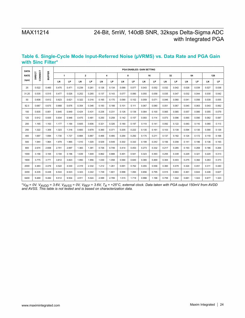
Table 6. Single-Cycle Mode Input-Referred Noise (µVRMS) vs. Data Rate and PGA Gain with Sinc Filter*
*VIN = 0V. VAVDD = 3.6V, VAVSS = 0V, VREF = 3.6V, TA = +25°C, external clock. Data taken with PGA output 150mV from AVDD and AVSS. This table is not tested and is based on characterization data.
DATA
RATE
(sps) DIR
ECT
CO
NN
ECT
BU
FFER
PGA ENABLED: GAIN SETTING
1 2 4 8 16 32 64 128
LN LP LN LP LN LP LN LP LN LP LN LP LN LP LN LP
25 0.522 0.460 0.475 0.471 0.239 0.261 0.126 0.134 0.068 0.077 0.043 0.052 0.032 0.042 0.028 0.039 0.027 0.038
31.25 0.535 0.515 0.477 0.526 0.252 0.265 0.137 0.143 0.077 0.080 0.050 0.058 0.035 0.047 0.032 0.044 0.030 0.042
50 0.608 0.612 0.623 0.621 0.322 0.316 0.165 0.170 0.090 0.102 0.059 0.071 0.046 0.060 0.041 0.056 0.039 0.055
62.5 0.687 0.675 0.668 0.676 0.354 0.346 0.183 0.188 0.101 0.111 0.067 0.080 0.051 0.067 0.045 0.063 0.043 0.062
100 0.835 0.851 0.845 0.849 0.424 0.431 0.226 0.231 0.126 0.139 0.084 0.100 0.065 0.085 0.057 0.080 0.055 0.079
125 0.912 0.935 0.934 0.948 0.475 0.481 0.250 0.258 0.142 0.157 0.093 0.114 0.073 0.096 0.065 0.090 0.062 0.087
200 1.165 1.163 1.177 1.184 0.605 0.606 0.321 0.326 0.180 0.197 0.119 0.141 0.092 0.122 0.083 0.116 0.080 0.113
250 1.322 1.309 1.323 1.316 0.683 0.679 0.360 0.371 0.205 0.222 0.135 0.161 0.103 0.139 0.094 0.130 0.090 0.129
400 1.697 1.694 1.730 1.727 0.884 0.887 0.466 0.485 0.264 0.292 0.175 0.211 0.137 0.182 0.124 0.172 0.118 0.168
500 1.944 1.964 1.979 1.965 1.010 1.020 0.529 0.549 0.302 0.332 0.199 0.242 0.156 0.208 0.141 0.196 0.136 0.193
800 2.674 2.658 2.701 2.697 1.383 1.391 0.726 0.749 0.414 0.453 0.273 0.332 0.217 0.285 0.193 0.269 0.186 0.264
1000 3.156 3.165 3.194 3.196 1.639 1.649 0.862 0.888 0.491 0.541 0.323 0.393 0.255 0.339 0.229 0.321 0.220 0.313
1600 3.775 3.771 3.812 3.823 1.950 1.956 1.030 1.058 0.584 0.640 0.385 0.469 0.304 0.403 0.275 0.382 0.263 0.373
2000 4.483 4.476 4.522 4.530 2.319 2.332 1.212 1.261 0.691 0.762 0.455 0.556 0.360 0.479 0.324 0.451 0.311 0.440
3200 6.435 6.448 6.544 6.523 3.343 3.342 1.749 1.801 0.998 1.094 0.656 0.795 0.515 0.683 0.461 0.644 0.446 0.627
6400 9.469 9.484 9.512 9.504 4.911 5.024 2.599 2.789 1.515 1.719 0.998 1.196 0.759 1.042 0.681 1.043 0.677 1.323
MAX11214 24-Bit, 5mW, 140dB SNR, 32ksps Delta-Sigma ADC with Integrated PGA
www.maximintegrated.com Maxim Integrated │ 24

Power-On ResetThe MAX11214 contains power-on reset (POR) supply monitoring circuitry on both the digital supply (DVDD) and the positive analog supply (AVDD). The POR circuitry ensures proper device default conditions after either a digital or analog power-sequencing event.The digital POR trigger threshold is typically 1.2V with respect to VDGND and has 100mV of hysteresis. The ana-log POR trigger threshold is typically 1.25V with respect to VAVSS and has 100mV of hysteresis. Both POR circuits have lowpass filters that prevent high-frequency supply glitches from triggering the POR.
Power-Down ModesThe MAX11214 can be powered down via the IMPD bit in the command byte (see Table 10). The PD[1:0] bits of the CTRL1 register are used to select the power-down state. The SPI remains fully functional in all power-down states.
Sleep Mode: The sleep mode can be set by writing 01 to the PD[1:0] bits. In this state the internal subregulator that powers the digital core is powered off. This is the lowest power state for the device.Standby Mode (10): The standby mode is set by writ-ing 10 to the PD[1:0] bits. In this mode the device is not active, but the internal subregulator is still powered on. This allows conversions to start immediately after receiv-ing a start conversion command (see Table 10).
Table 7. MAX11214 Command Behavior from Pin (RSTB, SYNC) and SPI (RESET, SYNC_SPI)
COMMAND ISSUED
COMMAND- ISSUED VIA
STATE BEFORE
COMMAND
STATE AFTER
COMMAND
TRANSITION TIME (MAX)
COMMAND INTERPRETATION AND RESULTING CHIP STATE
RESET SPI or PIN SPI, PIN
STBY STBY — Chip POR
SLEEP STBY 5ms Chip POR
Calibration STBY — Calibration stops, chip POR
Conversion STBY — Conversion stops, chip POR
IMPDCTRL1:PD=’01’ SLEEP Mode
SPI
STBY SLEEP — Chip changes from STBY to SLEEP
SLEEP SLEEP — Chip remains in SLEEP
Calibration SLEEP — Calibrations stop
Conversion SLEEP — Conversion stop
IMPDCTRL1:PD=’10’
STBY ModeSPI
STBY STBY — Chip remains in standby
SLEEP STBY — Chip changes from SLEEP to standby
Calibration STBY — Calibrations stop, chip changes to standby
Conversion STBY — Conversions stop, chip changes to standby
MAX11214 24-Bit, 5mW, 140dB SNR, 32ksps Delta-Sigma ADC with Integrated PGA
www.maximintegrated.com Maxim Integrated │ 25
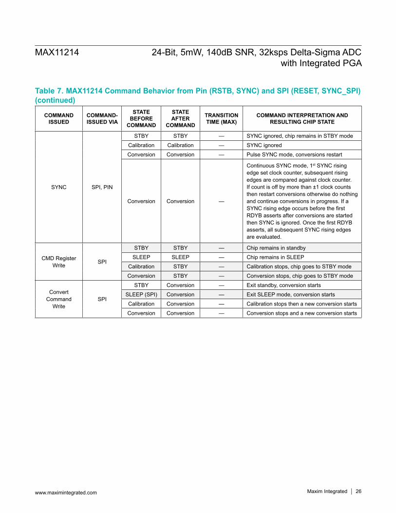
COMMAND ISSUED
COMMAND- ISSUED VIA
STATE BEFORE
COMMAND
STATE AFTER
COMMAND
TRANSITION TIME (MAX)
COMMAND INTERPRETATION AND RESULTING CHIP STATE
SYNC SPI, PIN
STBY STBY — SYNC ignored, chip remains in STBY mode
Calibration Calibration — SYNC ignored
Conversion Conversion — Pulse SYNC mode, conversions restart
Conversion Conversion —
Continuous SYNC mode, 1st SYNC rising edge set clock counter, subsequent rising edges are compared against clock counter. If count is off by more than ±1 clock counts then restart conversions otherwise do nothing and continue conversions in progress. If a SYNC rising edge occurs before the first RDYB asserts after conversions are started then SYNC is ignored. Once the first RDYB asserts, all subsequent SYNC rising edges are evaluated.
CMD Register Write SPI
STBY STBY — Chip remains in standby
SLEEP SLEEP — Chip remains in SLEEP
Calibration STBY — Calibration stops, chip goes to STBY mode
Conversion STBY — Conversion stops, chip goes to STBY mode
ConvertCommand
WriteSPI
STBY Conversion — Exit standby, conversion starts
SLEEP (SPI) Conversion — Exit SLEEP mode, conversion starts
Calibration Conversion — Calibration stops then a new conversion starts
Conversion Conversion — Conversion stops and a new conversion starts
Table 7. MAX11214 Command Behavior from Pin (RSTB, SYNC) and SPI (RESET, SYNC_SPI) (continued)
MAX11214 24-Bit, 5mW, 140dB SNR, 32ksps Delta-Sigma ADC with Integrated PGA
www.maximintegrated.com Maxim Integrated │ 26

Digital FiltersThe digital filter is a mode-configurable digital filter and decimator that processes a one-bit data stream from the fourth order delta-sigma modulator and implements a fifth order SINC function with an averaging function to produce a 24-bit wide data stream.
SINC FilterThe SINC filter allows MAX11214 to achieve very high SNR. One feature of the fifth order SINC filter is a band-width that is about twenty percent of the data rate. The
following example shows 3dB BW of about 1.5kHz for 8ksps data rate.
FIR FilterThe user can select the built-in FIR filter to expand the input bandwidth of MAX11214, thus achieving very low ripple passband with extremely sharp rolloff and high stopband rejection. This is done by selecting the FILT bits in the CTRL 3 register to enable the FIR filter. There are two different forms of FIR filter available, and the user can
Figure 3. Digital Filter Path
Figure 4a. SINC Magnitude Response Figure 4b. SINC Mag Response Zoomed-In
MODULATOR SINC FIR LPF LINEAR PHASE
FIR LPF MINIMUM PHASE
FIR LPF LINEAR PHASE
PROGRAMM-ABLE
IIRHPF
MAX11214 24-Bit, 5mW, 140dB SNR, 32ksps Delta-Sigma ADC with Integrated PGA
www.maximintegrated.com Maxim Integrated │ 27

select between linear phase response or minimum phase response by setting the PHASE bit in the CTRL 3 register.The magnitude response for FIR filter with linear phase and minimum phase at 8ksps data rate is shown below:The passband ripple is comparable in linear phase and minimum phase responses and is less than 5mdB.
Linear response FIR filter should be selected if the appli-cation requires linear phase relationship, otherwise for faster settling use minimum phase FIR filter. This is shown in the following phase response and step response plots. Note all plots are taken for 8ksps data rate.
Figure 5. Magnitude Response, Linear Phase FIR, 8ksps Data Rate
Figure 6. Magnitude Response, Minimum Phase FIR, 8ksps Data Rate
Figure 7. Passband Ripple, Linear Phase FIR, 8ksps Data Rate
Figure 8. Passband Ripple, Minimum Phase FIR, 8ksps Data Rate
MAX11214 24-Bit, 5mW, 140dB SNR, 32ksps Delta-Sigma ADC with Integrated PGA
www.maximintegrated.com Maxim Integrated │ 28

Figure 9. Phase Response, Linear Phase FIR, 8ksps Data Rate
Figure 10. Step Response, Linear Phase FIR
Figure 11. Phase Response, Minimum Phase FIR, 8ksps Data Rate
Figure 12. Step Response, Minimum Phase FIR
MAX11214 24-Bit, 5mW, 140dB SNR, 32ksps Delta-Sigma ADC with Integrated PGA
www.maximintegrated.com Maxim Integrated │ 29

Highpass FilterThe highpass filter in the MAX11214 has adjustable rolloff frequency and is used for DC or low-frequency removal from the output. The IIR option is enabled by setting the FILT bits to ‘11’ in the CTRL3 register (see Table 12). The 16-bit highpass filter configuration register HPF configures the corner frequency of the IIR (infinite impulse response) digital filter.The transfer function for the IIR filter in z-domain is given by
1
12 a 1 ZHPF(Z)
2 1 b Z
−
−− −
= ×− ⋅
where b is calculated from:
( )21 1 ab
2+ −
=
The ideal HPF gain response is:
cos sin 11 1 2cos
| |cos sin 12
cos
+ −+ −
= + −
−
N N
N
N N
N
w ww
HPFw w
w
where the normalized 3dB corner frequency is given by:
2= HPN
S
fwf
π
fHP is the highpass cutoff frequency and fS is the data rate.To solve for the programmable register HPF value, use:
[15:0]cos sin 165536 1 1 2
cos
+ − = × − −
N N
N
w wHPFRw
Using the maximum Highpass Filter Register value typi-cally gives 3dB rolloff equivalent to one tenth of the data rate. Note that not all values are allowed. Table 8 shows what maximum values HPF[15:0] can take for different data rates.Table 9 shows a few examples of calculations for 3dB corner frequency.
Table 8. Max HPF[15:0] Register Values for Different Data Rates
Table 9. Examples of HPF[15:0] Register Values and Cutoff Frequencies
CASE FHP DATA RATE HPF[15:0] MAX VALUE1 25 250 56492
2 102 1000 61787
3 204 2000 61787
4 409 4000 63164
CASE -3dB CORNER FREQUENCY (Hz) HPF[15:0]
1 0.002Fs 823 (decimal)
2 0.001Fs 410 (decimal)
3 0.0005Fs 203 (decimal)
MAX11214 24-Bit, 5mW, 140dB SNR, 32ksps Delta-Sigma ADC with Integrated PGA
www.maximintegrated.com Maxim Integrated │ 30

Serial InterfaceThe MAX11214 interface is fully compatible with SPI, QSPI™, and MICROWIRE®-standard serial interfaces. The SPI interface provides access to on-chip registers that are 8 bits to 24 bits wide.
Chip Select (CSB)CSB is an active-low chip-select input to communicate with the MAX11214. CSB transitioning from low to high is used to reset the SPI interface. When CSB is low, data is clocked into the device from DIN on the rising edge of SCLK. Data is clocked out of DOUT on the falling edge of SCLK. When CSB is high, SCLK and DIN are ignored and DOUT is high impedance allowing DOUT to be shared with other devices.
SCLK (Serial Clock)The serial clock (SCLK) is used to synchronize data com-munication between the host device and the MAX11214. Data is shifted in on the rising edge of SCLK and data is shifted out on the falling edge of SCLK. SCLK remains low when not active.
DIN (Serial Data Input)Data present on DIN is clocked into internal registers on the rising edge of SCLK.
DOUT (Serial Data Output)The DOUT pin is actively driven when CSB is low and high impedance when CSB is high. Data are shifted out on DOUT on the falling edge of SCLK.
Data Ready (RDYB)The RDYB output displays the conversion status. RDYB is forced low when a conversion result is ready for read-out and remains low until the user reads the conversion result. RDYB returns high after SCLK is pulled high, fol-lowing a complete read of the data register. RDYB also resets high for 4 master clock cycles prior to DATA regis-ter update (see Figure 13).When the modulator is in one of the continuous operat-ing modes and the part has either experienced a RESET, SYNC, or POR event, then the RDYB pin will remain high until the selected filter is settled. If the SINC filter is selected then RDYB remains high for five tCNV times and afterwards data appears at each tCNV.The conversion status can also be determined by reading the MSTAT bit in the STAT1 register.
QSPI is a trademark of Motorola, Inc. MICROWIRE is a registered trademark of National Semiconductor Corp.
RDYB
62 tCNV
CSB/SCLK/DIN
RDYBSCYCLE=’1',CONTSC=’1',FLT=’00' or ‘01’
SCYCLE=’0',CONTSC=’x',FLT=’10' or ‘11’
RDYB
tCNV
SCYCLE=’1',CONTSC=’0',FLT=’00' or ‘01’
RDYB
5 tCNV
SCYCLE=’0',CONTSC=’x',FLT=’00' or ‘01’
DATA NOT RETRIEVED
DATARETRIEVED
CONVERT COMMANDS
tCNV
tCNV
tCNV
tCNV
Figure 13. DATA Ready Timing for All Conversion Modes
MAX11214 24-Bit, 5mW, 140dB SNR, 32ksps Delta-Sigma ADC with Integrated PGA
www.maximintegrated.com Maxim Integrated │ 31
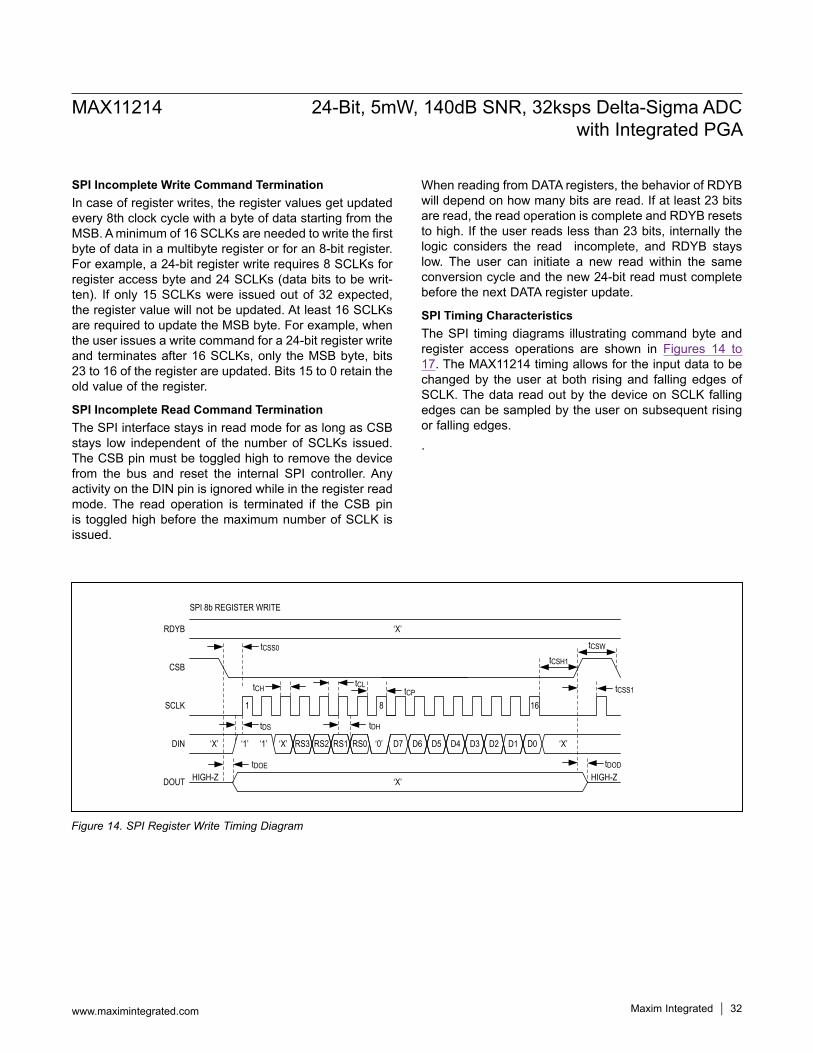
SPI Incomplete Write Command TerminationIn case of register writes, the register values get updated every 8th clock cycle with a byte of data starting from the MSB. A minimum of 16 SCLKs are needed to write the first byte of data in a multibyte register or for an 8-bit register. For example, a 24-bit register write requires 8 SCLKs for register access byte and 24 SCLKs (data bits to be writ-ten). If only 15 SCLKs were issued out of 32 expected, the register value will not be updated. At least 16 SCLKs are required to update the MSB byte. For example, when the user issues a write command for a 24-bit register write and terminates after 16 SCLKs, only the MSB byte, bits 23 to 16 of the register are updated. Bits 15 to 0 retain the old value of the register.
SPI Incomplete Read Command TerminationThe SPI interface stays in read mode for as long as CSB stays low independent of the number of SCLKs issued. The CSB pin must be toggled high to remove the device from the bus and reset the internal SPI controller. Any activity on the DIN pin is ignored while in the register read mode. The read operation is terminated if the CSB pin is toggled high before the maximum number of SCLK is issued.
When reading from DATA registers, the behavior of RDYB will depend on how many bits are read. If at least 23 bits are read, the read operation is complete and RDYB resets to high. If the user reads less than 23 bits, internally the logic considers the read incomplete, and RDYB stays low. The user can initiate a new read within the same conversion cycle and the new 24-bit read must complete before the next DATA register update.
SPI Timing CharacteristicsThe SPI timing diagrams illustrating command byte and register access operations are shown in Figures 14 to 17. The MAX11214 timing allows for the input data to be changed by the user at both rising and falling edges of SCLK. The data read out by the device on SCLK falling edges can be sampled by the user on subsequent rising or falling edges. .
SCLK
RDYB
DIN
CSB
DOUT
1 8
HIGH-Z HIGH-Z
tCSS0
tDS
tDOE
tDH
tDOD
tCSS1tCH tCLtCP
tCSH1
‘X’ ‘1’ ‘1’ RS2‘X’ RS3
tCSW
‘X’
SPI 8b REGISTER WRITE
RS1 RS0
‘X’
16
D7‘0’ D6 D5 D4 D3 D2 D1 D0 ‘X’
Figure 14. SPI Register Write Timing Diagram
MAX11214 24-Bit, 5mW, 140dB SNR, 32ksps Delta-Sigma ADC with Integrated PGA
www.maximintegrated.com Maxim Integrated │ 32

Figure 15. SPI Register Read Timing Diagram
Figure 16. SPI Data Readout Timing Diagram
SCLK
RDYB
DIN
CSB
DOUT
1 8
HIGH-Z HIGH-Z
tCSS0
tDS
tDOE
tDH
tDOD
tCSS1tCH tCL tCP
tCSH1
‘X’ ‘1’ ‘1’ RS2RS4 RS3
tCSW
‘X’
SPI 8b REGISTER READ
RS1 RS0
‘X’
16
‘1’ ‘X’
D7 D6 D5 D4 D3 D2 D1 D0
‘X’ ‘X’ ‘X’ ‘X’ ‘X’ ‘X’ ‘X’ ‘X’
tDOT tDOH
8b data
SCLK
RDYB
DIN
CSB
DOUT MSB
1 8 9
LSBHIGH-Z
3139
23 16b data24b data32b data
HIGH-Z
tCSS0
tDS
tDOE
tDH
tDOT tDOH tDOD
tR1
tCSS1tCH tCL tCP
tCSH1
tCSW
‘x’ ‘1’ ‘1’ ‘1’ ‘1’ ‘1’‘0’ ‘0’ ‘0’
‘x’
MAX11214 24-Bit, 5mW, 140dB SNR, 32ksps Delta-Sigma ADC with Integrated PGA
www.maximintegrated.com Maxim Integrated │ 33
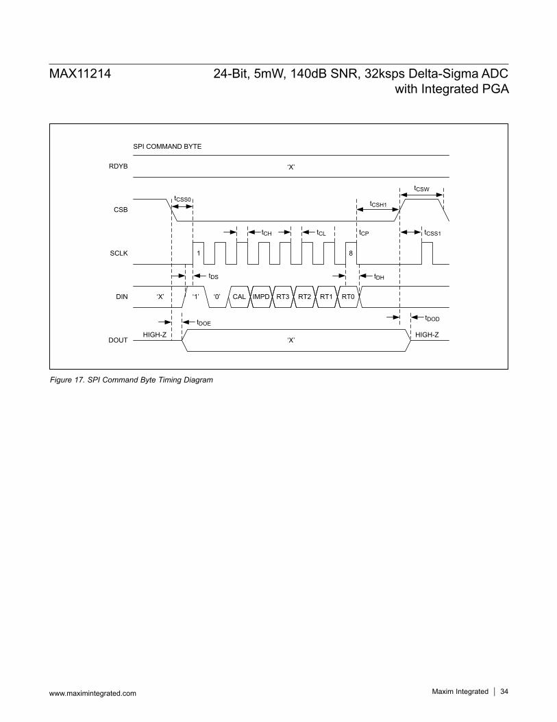
SCLK
RDYB
DIN
CSB
DOUT
1 8
HIGH-Z HIGH-Z
tCSS0
tDS
tDOE
tDH
tDOD
tCSS1tCH tCL tCP
tCSH1
‘X’ ‘1’ ‘0’ IMPDCAL
tCSW
‘X’
SPI COMMAND BYTE
RT2 RT1 RT0
‘X’
RT3
Figure 17. SPI Command Byte Timing Diagram
MAX11214 24-Bit, 5mW, 140dB SNR, 32ksps Delta-Sigma ADC with Integrated PGA
www.maximintegrated.com Maxim Integrated │ 34

Modes and RegistersThe MAX11214 interface operates in two modes, conversion mode or register access mode, which is selected by the command byte. Every SPI transaction to the MAX11214 starts with a command byte. The command byte begins with a START bit (B7), which must be set to 1. The next bit is the MODE bit (B6), which selects between conversion mode or register access mode. Based on the mode selection the remaining bits in the command byte get decoded accordingly.If the command byte is for a register read/write request, hold CSB low for the entire read or write operation and pull CSB high at the end of the command. For example, if the command is to read a 24-bit data register; hold CSB low for 32 SCLK cycles (8 cycles of command plus 24 cycles of data). CSB transitions must not occur near the rising edge of SCLK and must conform to the setup and hold timing detailed in the timing section.Pulling CSB from low to high ends the current SPI transaction. If CSB is pulled high in the middle of a register write com-mand, the registers will retain any partially written data. This does not cause a change in state of any internal register that was being accessed for read or write
Conversion Mode (MODE = 0)
Set the MODE bit to 0 to: start a conversion with a rate defined by RATE[3:0], immediately power down the part or per-form a calibration.The CAL bit (B5) determines if a calibration is to be performed. Set CAL = 1 to perform a calibration, for all other opera-tions set CAL = 0. The calibration is done based on the setting of the calibration bits CTRL 5. Also see discussion on calibration in the following sections.The IMPD bit (B4) controls the software power-down. Set IMPD = 1 to power down the MAX11214 and enter sleep mode or standby mode, based on the setting of the PD Bits in CTRL1, once the command byte is complete. The power-down status does not change until another command byte is received that is interpreted as a conversion byte (MODE = 0, IMPD = 0). Set IMPD = 0 for normal operation.The data rate bits RATE[3:0] determine the conversion speed. The speed table is shown later in Table 13.
Register Access Mode (MODE = 1)
MODE 1 or Register Access Mode is used for reading from and writing to the registers of the MAX11214. Set the MODE bit (B6) = 1 to configure the command byte for Register Access Modes.The bits RS[4:0] determine the register that is addressed as shown in Table 12.The R/W bit enables either a read or a write of the register. Set R/W = 0 to write to the selected register and R/W = 1 to read from the selected register.
Table 11. Command Byte for Register Access Mode (MODE = 1)BIT B7 (MSB) B6 B5 B4 B3 B2 B1 B0
BIT NAME START =1 MODE = 1 RS4 RS3 RS2 RS1 RS0 R/W
Table 10. Command Byte for Conversion Modes (MODE = 0)BIT B7 (MSB) B6 B5 B4 B3 B2 B1 B0
BIT NAME START = 1 MODE = 0 CAL IMPD RATE3 RATE2 RATE1 RATE0
MAX11214 24-Bit, 5mW, 140dB SNR, 32ksps Delta-Sigma ADC with Integrated PGA
www.maximintegrated.com Maxim Integrated │ 35

Register MapRegister Address MapThere are 14 registers that can be accessed in the MAX11214. The majority of registers can be both written to and read from, but the STAT and DATA registers are read only. The RAM and SYNC are not physical registers, but addresses to enable special operating modes.
Table 12. Register Address Map
REGISTER NAME R/W
ADDRESS SELECTRS[3:0]
B7 B6 B5 B4 B3 B2 B1 B0
STAT R 0x0INRESET ERROR — — PDSTAT1 PDSTAT0 RDERR AOR
RATE3 RATE2 RATE1 RATE0 SYSGOR DOR MSTAT RDY
CTRL1 R/W 0x1 EXTCK SYNCMODE PD1 PD0 U/~B FORMAT SCYCLE CONTSC
CTRL2 R/W 0x2 DGAIN1 DGAIN0 BUFEN LPMODE PGAEN PGAG2 PGAG1 PGAG0
CTRL3 R/W 0x3 — — ENMSYNC MODBITS DATA32 PHASE FILT1 FILT0
CTRL4 R/W 0x4 — DIR3 DIR2 DIR1 — DIO3 DIO2 DIO1
CTRL5 R/W 0x5 CAL1 CAL0 — — NOSYSG NOSYSO NOSCG NOSCO
DATA R 0x6 D[23:0]
SOC_SPI R/W 0x7 B[23:0]
SGC_SPI R/W 0x8 B[23:0]
SCOC_SPI R/W 0x9 B[23:0]
SCGC_SPI R/W 0xA B[23:0]
HPF R/W 0xB B[15:0]
RAM R/W 0xCAddress space only, not a physical register. Please contact factory for instructions on using internal RAM function.
SYNC_SPI W 0xDAddress space only, not a physical register. Please contact factory for instructions on using internal RAM function.
SOC_ADC R 0x15 B[23:0]
SGC_ADC R 0x16 B[23:0]
SCOC_ADC R 0x17 B[23:0]
SCGC_ADC R 0x18 B[23:0]
MAX11214 24-Bit, 5mW, 140dB SNR, 32ksps Delta-Sigma ADC with Integrated PGA
www.maximintegrated.com Maxim Integrated │ 36
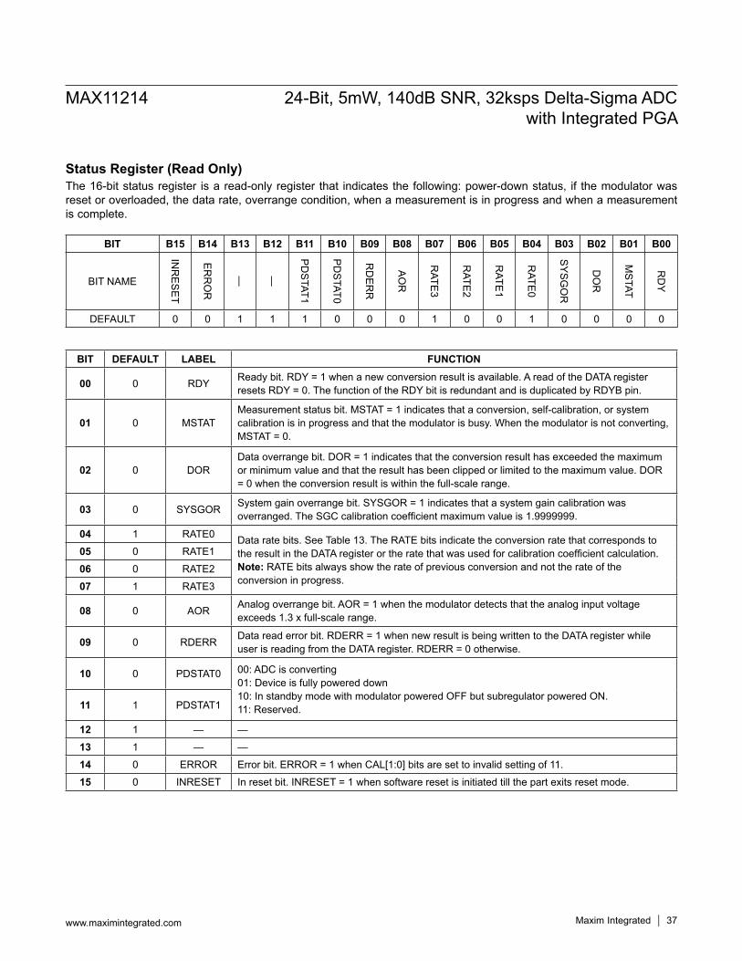
Status Register (Read Only)The 16-bit status register is a read-only register that indicates the following: power-down status, if the modulator was reset or overloaded, the data rate, overrange condition, when a measurement is in progress and when a measurement is complete.
BIT B15 B14 B13 B12 B11 B10 B09 B08 B07 B06 B05 B04 B03 B02 B01 B00
BIT NAME
INR
ES
ET
ER
RO
R
— —
PD
STAT1
PD
STAT0
RD
ER
R
AO
R
RATE
3
RATE
2
RATE
1
RATE
0
SY
SG
OR
DO
R
MS
TAT
RD
Y
DEFAULT 0 0 1 1 1 0 0 0 1 0 0 1 0 0 0 0
BIT DEFAULT LABEL FUNCTION
00 0 RDY Ready bit. RDY = 1 when a new conversion result is available. A read of the DATA register resets RDY = 0. The function of the RDY bit is redundant and is duplicated by RDYB pin.
01 0 MSTATMeasurement status bit. MSTAT = 1 indicates that a conversion, self-calibration, or system calibration is in progress and that the modulator is busy. When the modulator is not converting, MSTAT = 0.
02 0 DORData overrange bit. DOR = 1 indicates that the conversion result has exceeded the maximum or minimum value and that the result has been clipped or limited to the maximum value. DOR = 0 when the conversion result is within the full-scale range.
03 0 SYSGOR System gain overrange bit. SYSGOR = 1 indicates that a system gain calibration was overranged. The SGC calibration coefficient maximum value is 1.9999999.
04 1 RATE0 Data rate bits. See Table 13. The RATE bits indicate the conversion rate that corresponds to the result in the DATA register or the rate that was used for calibration coefficient calculation. Note: RATE bits always show the rate of previous conversion and not the rate of the conversion in progress.
05 0 RATE1
06 0 RATE2
07 1 RATE3
08 0 AOR Analog overrange bit. AOR = 1 when the modulator detects that the analog input voltage exceeds 1.3 x full-scale range.
09 0 RDERR Data read error bit. RDERR = 1 when new result is being written to the DATA register while user is reading from the DATA register. RDERR = 0 otherwise.
10 0 PDSTAT0 00: ADC is converting01: Device is fully powered down10: In standby mode with modulator powered OFF but subregulator powered ON.11: Reserved.11 1 PDSTAT1
12 1 — —
13 1 — —
14 0 ERROR Error bit. ERROR = 1 when CAL[1:0] bits are set to invalid setting of 11.
15 0 INRESET In reset bit. INRESET = 1 when software reset is initiated till the part exits reset mode.
MAX11214 24-Bit, 5mW, 140dB SNR, 32ksps Delta-Sigma ADC with Integrated PGA
www.maximintegrated.com Maxim Integrated │ 37

Table 13. Programmable Conversion RatesCONTINUOUS DATA RATE, SCYCLE = 0
RATE [3:0] SINC FILTER (sps) FIR FILTER (sps)SCYCLE = 1 SINGLE
-CYCLE CONTINUOUS DATA RATE (sps)
0000 0.95 — 25
0001 1.9 — 31.25
0010 3.9 — 50
0011 7.8 — 62.5
0100 15.6 — 100
0101 31.25 — 125
0110 62.5 62.5 200
0111 125 125 250
1000 250 250 400
1001 500 500 500
1010 1000 1000 800
1011 2000 2000 1000
1100 4000 4000 1600
1101 8000 8000 2000
1110 16000 — 3200
1111 32000 — 6400
*Continuous data rate with SCYCLE = 0, single cycle with CONTSC = 1, SCYCLE = 1. The FIR filter can only run in continuous con-version mode.
MAX11214 24-Bit, 5mW, 140dB SNR, 32ksps Delta-Sigma ADC with Integrated PGA
www.maximintegrated.com Maxim Integrated │ 38

Control RegistersThese are registers reserved for configuring the MAX11214.
Control 1 Register (Read/Write)The CTRL1 register is an 8-bit read/write register. The byte written to the CTRL1 register determines the clock setting, synchronization mode, power-down or reset state, input range is unipolar or bipolar, data output is two’s complement or offset binary, and conversion mode is in single cycle or continuous.
BIT B07 B06 B05 B04 B03 B02 B01 B00
BIT NAME EXTCK SYNC PD1 PD0 U/B FORMAT SCYCLE CONTSC
DEFAULT 0 0 0 0 0 0 1 0
BIT DEFAULT LABEL FUNCTION
00 0 CONTSC Continuous single-cycle bit. Set CONTSC = 1 to select continuous conversions. Set CONTSC = 0 to select a single conversion.
01 1 SCYCLESingle-cycle control bit. Set SCYCLE = 1 to select single-cycle mode. The MAX11214 completes one no-latency conversion and then powers down into a leakage-only state. Set SCYCLE = 0 to select continuous conversion mode.
02 0 FORMATBipolar range format bit. When reading bipolar data, set FORMAT = 0 to select two’s complement and FORMAT = 1 to select offset binary. The data from unipolar range is always formatted in offset binary format.
03 0 U/B U/B: Unipolar/bipolar bit. Set U/B = 1 to select the unipolar input range (0 to VREF). Set U/B = 0 to select the bipolar input range (±VREF).
04 0 PD0
00 Normal power-up state. This is the default state.
01 Sleep Mode—Powers down the subregulator and the entire digital circuitry. Upon resumption of power to the digital the PD[1:0] reverts to the default state of ‘00’.
05 0 PD1
10 Standby power—Powers down the analog blocks leaving the subregulator powered up.
11 Resets all registers to POR state leaving the subregulator powered. The PD[1:0] bits are reset to ‘00’. The operation of this state is identical to the RSTB pin.
06 0 SYNC Set SYNC = 1 to select continuous synchronization mode. Set SYNC = 0 to select pulse synchronization mode.
07 0 EXTCK External clock bit. Set EXTCLK = 1 to selects the external clock as the system clock. Set EXTCLK = 0 to select the internal oscillator as the system clock.
MAX11214 24-Bit, 5mW, 140dB SNR, 32ksps Delta-Sigma ADC with Integrated PGA
www.maximintegrated.com Maxim Integrated │ 39

Control 2 Register (Read/Write)The CTRL2 register is an 8-bit read/write register. The byte written to the CTRL2 register determines the digital and analog gain settings, and whether the buffers or PGA is enabled.
BIT B07 B06 B05 B04 B03 B02 B01 B00BIT NAME DGAIN1 DGAIN0 BUFEN LPMODE PGAEN PGAG2 PGAG1 PGAG0
DEFAULT 0 0 0 0 0 0 0 0
BIT DEFAULT LABEL FUNCTION
00 0 PGA0 000001010011100101110111
X1 PGA Gain-Setting bitsX2X4X8X16X32X64X128
01 0 PGA1
02 0 PGA2
03 0 PGAEN PGA Enable Bit. Set PGAEN = 1 to enable the PGA. Set PGAEN = 0 to disable the PGA.
04 0 LPMODE PGA Low Power. Set LPMODE = 1 for lower power. Set LPMODE = 0 for standard power.
05 0 BUFEN Analog input buffer enable bit. Set BUFEN = 1 to enable the analog input buffers. Set BUFEN = 0 to disable the analog input buffers.
06 0 DGAIN000 x1 Modulator Digital Gain Bits
01 x2
07 0 DGAIN110 x4
11 x8
MAX11214 24-Bit, 5mW, 140dB SNR, 32ksps Delta-Sigma ADC with Integrated PGA
www.maximintegrated.com Maxim Integrated │ 40
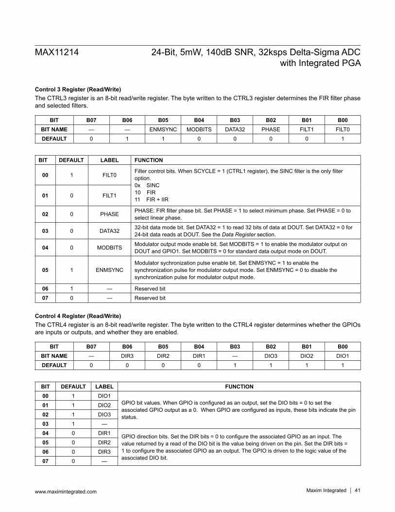
Control 3 Register (Read/Write)The CTRL3 register is an 8-bit read/write register. The byte written to the CTRL3 register determines the FIR filter phase and selected filters.
Control 4 Register (Read/Write)The CTRL4 register is an 8-bit read/write register. The byte written to the CTRL4 register determines whether the GPIOs are inputs or outputs, and whether they are enabled.
BIT B07 B06 B05 B04 B03 B02 B01 B00BIT NAME — — ENMSYNC MODBITS DATA32 PHASE FILT1 FILT0
DEFAULT 0 1 1 0 0 0 0 1
BIT DEFAULT LABEL FUNCTION
00 1 FILT0Filter control bits. When SCYCLE = 1 (CTRL1 register), the SINC filter is the only filter option. 0x SINC10 FIR11 FIR + IIR
01 0 FILT1
02 0 PHASE PHASE: FIR filter phase bit. Set PHASE = 1 to select minimum phase. Set PHASE = 0 to select linear phase.
03 0 DATA32 32-bit data mode bit. Set DATA32 = 1 to read 32 bits of data at DOUT. Set DATA32 = 0 for 24-bit data reads at DOUT. See the Data Register section.
04 0 MODBITS Modulator output mode enable bit. Set MODBITS = 1 to enable the modulator output on DOUT and GPIO1. Set MODBITS = 0 for standard data output mode on DOUT.
05 1 ENMSYNCModulator sychronization pulse enable bit. Set ENMSYNC = 1 to enable the synchronization pulse for modulator output mode. Set ENMSYNC = 0 to disable the synchronization pulse for modulator output mode.
06 1 — Reserved bit
07 0 — Reserved bit
BIT B07 B06 B05 B04 B03 B02 B01 B00BIT NAME — DIR3 DIR2 DIR1 — DIO3 DIO2 DIO1
DEFAULT 0 0 0 0 1 1 1 1
BIT DEFAULT LABEL FUNCTION00 1 DIO1
GPIO bit values. When GPIO is configured as an output, set the DIO bits = 0 to set the associated GPIO output as a 0. When GPIO are configured as inputs, these bits indicate the pin status.
01 1 DIO2
02 1 DIO3
03 1 —
04 0 DIR1 GPIO direction bits. Set the DIR bits = 0 to configure the associated GPIO as an input. The value returned by a read of the DIO bit is the value being driven on the pin. Set the DIR bits = 1 to configure the associated GPIO as an output. The GPIO is driven to the logic value of the associated DIO bit.
05 0 DIR2
06 0 DIR3
07 0 —
MAX11214 24-Bit, 5mW, 140dB SNR, 32ksps Delta-Sigma ADC with Integrated PGA
www.maximintegrated.com Maxim Integrated │ 41

Control 5 Register (Read/Write)The CTRL5 register is an 8-bit read/write register. The byte written to the CTRL5 register determines the MAX11214’s reset, data overflow, and calibration modes.
Data Register (Read Only)The data register is a 32-bit or 24-bit read-only register. Any attempt to write data to the data register has no effect. The data from this register is clocked out MSB first. The data register holds the conversion result. The result is stored in either two’s complement or offset binary format, depending on the FORMAT bit in CTRL1 register. The data format in unipolar mode is always offset binary. In bipolar mode, set the FORMAT bit = 1 for offset binary or FORMAT = 0 for two’s compliment. Any input exceeding the available input range is limited to the minimum or maximum data value. Attempts to read this register while data is being updated (4 system clocks before RDYB asserts low) will result in invalid data being read, see Figure 13. Note that the STATUS register RDERR bit is set when this condition is detected.
BIT B07 B06 B05 B04 B03 B02 B01 B00BIT NAME CAL1 CAL0 — — NOSYSG NOSYSO NOSCG NOSCO
DEFAULT 0 0 0 0 1 1 0 0
BIT DEFAULT LABEL FUNCTION
00 0 NOSCO
No self-calibration offset bit. Set NOSCO = 1 to disable the use of the self-calibration offset value when computing the final offset and gain-corrected data value. Set NOSCO = 0 to enable the use of the self-calibration offset value when computing the final offset and gain-corrected data value.
01 0 NOSCG
No self-calibration gain bit. Set NOSCG = 1 to disable the use of the self-calibration gain value when computing the final offset and gain-corrected data value. Set NOSCG = 0 to enable the use of the self-calibration gain value when computing the final offset and gain-corrected data value.
02 1 NOSYSONo system offset bit. Set NOSYSO = 1 to disable the use of the system offset value when computing the final offset and gain-corrected data value. Set NOSYSO = 0 to enable the use of the system offset value when computing the final offset-corrected data value.
03 1 NOSYSGNo system gain bit. Set NOSYSG = 1 to disable the use of the system gain value when computing the final offset and gain-corrected data value. Set NOSYSG = 0 to enable the use of the system gain value when computing the final gain-corrected data value.
04 0 — Reserved
05 0 — Reserved
06 0 CAL0 00 Perform Self Calibration01 Perform System-Level Offset Calibration10 Perform System-Level Full-Scale Calibration11 Reserved07 0 CAL1
BIT B31 B30 B29 B28 B27 B26 B25 B24 B23 B22 B21 B20 B19 B18 B17 B16 B15 B14 B13 B12 B11 B10 B09 B08 B07 B06 B05 B04 B03 B02 B01 B00
DEFAULT 0 0 0 0 0 0 0 0 0 0 0 0 0 0 0 0 0 0 0 0 0 0 0 0 0 0 0 0 0 0 0 0
MAX11214 24-Bit, 5mW, 140dB SNR, 32ksps Delta-Sigma ADC with Integrated PGA
www.maximintegrated.com Maxim Integrated │ 42

CalibrationTwo types of calibration are available: self-calibration and system calibration. Self-calibration is used to reduce the MAX11214 gain and offset errors during changing operating conditions such as supply voltages, ambient temperature, and time. System calibration is used to reduce the gain and offset of the entire signal path. This enables calibration of board level components and the integrated PGA. System calibration requires the MAX11214 inputs to be reconfigured for zero scale and full scale during calibration. See Figure 18 for details of the calibration signal flow.The on-chip calibration registers are enabled or disabled by programming the NOSYSG, NOSYSO, NOSCG, and NOSCO bits in the CTRL5 register. See Table 12.
Self-CalibrationThe self-calibration is an internal operation and does not disturb the analog inputs. Self-calibration is accomplished in two independent phases, offset and gain. The first phase disconnects the inputs to the modulator and shorts them together internally to develop a zero-scale signal. A conversion is then completed and the results are post-processed to generate an offset coefficient which cancels all internally generated offsets. The second phase connects the inputs to the reference to develop a full-scale signal. A conversion is then completed and the results are post-processed to generate a full-scale coefficient, which scales the converters full-scale analog range to the full-scale digital range.The entire self-calibration sequence requires two independent conversions, one for offset and one for full scale.The conversion rate is 50sps which provides the lowest noise and most accurate calibrations. The self-calibration opera-tion excludes the PGA. A system-level calibration is available in order to calibrate the PGA signal path.The calibration operations are controlled with the CAL bit in the command byte. Request a self-calibration by setting the CAL bit to 1, with the CTRL5:CAL[1:0] = 00. A self-calibration requires 200ms to complete, and both the SCOC and SCGC registers contain the values that correct the chip output for zero scale and full scale.
System CalibrationThis mode is used when board level components and the integrated PGA calibration is desired. A system calibration requires the user to configure the input to the proper level for the calibration operation. The offset and full-scale system calibrations are performed using separate command bytes by configuring the CTRL5:CAL [1:0] bits. The system offset and system full scale require setting these CAL bits appropriately before issuing the calibration command byte.
Table 14. ADC Output Code Data Format
CODE TRANSITION
ANALOG INPUT (AINP - AINN) (V)
DIGITAL OUTPUT CODE (Hex)OFFSET BINARY TWO’s COMPLEMENT
32-BIT 24-BIT 32-BIT 24-BIT≥ FS ≥ VREF FFFFFFFF FFFFFF 7FFFFFFF 7FFFFF
FS – 1 LSB VREF x (1 – (1/2N – 1)) FFFFFFFE FFFFFE 7FFFFFFE 7FFFFE
Midscale + 1 LSB VREF/2N - 1 80000001 800001 00000001 000001
Midscale VREF/2N 80000000 800000 00000000 000000
Midscale - 1 LSB -VREF/2N -1 7FFFFFFF 7FFFFF FFFFFFFF FFFFFF
ZS + 1 LSB -VREF x (1 – (1/2N – 1)) 00000001 000001 80000001 800001
≤ ZS ≤ -VREF 00000000 000000 80000000 800000
N = number of data bits, 32 or 24.VREF = VREFP - VREFN.
MAX11214 24-Bit, 5mW, 140dB SNR, 32ksps Delta-Sigma ADC with Integrated PGA
www.maximintegrated.com Maxim Integrated │ 43
Request a system zero-scale calibration by setting the CAL bit to 1 and the CTRL5:CAL[1:0] bit = 01 and connect a system zero-level signal to the input pins. The system zero calibration requires 100ms to complete, and the SOC register contains values that correct the chip zero scale.Request a system full-scale calibration by setting the CAL bit to 1 and the CTRL5:CAL[1:0] = 10 and connect a system full-scale signal level to the input pins. The system full-scale calibration requires 100ms to complete, and the SGC register contains values that correct for the chip full-scale value.A third level of calibration allows a write to the internal calibration registers through the SPI interface to achieve any digital offset or scaling with the following restrictions. The range of digital offset correction is ±VREF/4. The resolution of offset correction is 0.5 LSB. The range of digital gain correction is from 0.75 to 2. The resolution of gain is less than 1ppm.
SPI System Offset Calibration Register (SOC_SPI)The system offset calibration register is a 24-bit read/write register. The data written/read to/from this register is clocked in/out MSB first. The format is always in two’s complement. This register temporarily holds the system offset calibration value from the user. Once a conversion command is requested, this value gets copied into the SOC_ADC register. The value written to this register remains until it is overwritten. This value gets invalidated for calibration after a system-calibration operation is requested. Any attempt to write to this register during an active calibration operation will be ignored.
ADC System Offset Calibration Register (SOC_ADC)This is 24-bit read only register. There are two ways this register value is updated. One way is if a system offset calibra-tion operation is requested. Another way is if a user writes a value to SOC_SPI register, the value will then get copied into SOC_ADC from SOC_SPI.The system offset calibration value is subtracted from each conversion result if NOSYSO = 0 in the CTRL5 register. The system offset calibration value is subtracted from the conversion result after self-calibration, but before system gain correction. It is also applied prior to the 1x or 2x scale factor associated with bipolar and unipolar modes. Attempts to read this register while data is being updated (4 system clocks before RDYB asserts low) will result in invalid data being read, see Figure 13. Note that the STATUS register RDERR bit is set when this condition is detected.
SPI System Gain Calibration Register (SGC_SPI)The system gain calibration register is a 24-bit read/write register. The data written/read to/from this register is clocked in/out MSB first. The format is unsigned binary. This register temporarily holds the system gain calibration value from the user. Once a conversion command is requested, this value gets copied into SGC_ADC register. The value written to this register remains until it is overwritten. This value gets invalidated for calibration after a system-calibration opera-tion is requested. Any attempt to write to this register during an active calibration operation will be ignored.
ADC System Gain Calibration Register (SGC_ADC)This is 24-bit read only register. There are two ways this register value is updated. One way is if a system gain calibration operation is requested. Another way is if a user writes a value to SGC_SPI register, the value will then get copied into SGC_ADC from SGC_SPI.The system gain calibration value is used to scale the offset-corrected conversion result if NOSYSG = 0 in the CTRL5 register. The system gain calibration value scales the gain corrected result by up to 2x or can correct a gain error of approximately 50%. The amount of positive gain error that can be corrected is determined by modulator overload characteristics which may be as much as +125%. The gain will be corrected to within 1ppm. Attempts to read this register while data is being updated (4 system clocks before RDYB asserts low) will result in invalid data being read, see Figure 13. Note that the STATUS register RDERR bit is set when this condition is detected.
MAX11214 24-Bit, 5mW, 140dB SNR, 32ksps Delta-Sigma ADC with Integrated PGA
www.maximintegrated.com Maxim Integrated │ 44

SPI Self-Cal Offset Calibration Register (SCOC_SPI)The Self-Cal Offset register is a 24-bit read/write register. The data written/read to/from this register is clocked in/out MSB first. The format is always in two’s complement format. This register temporarily holds the self-cal offset calibration value from the user. Once a conversion command is requested, this value gets copied into SCOC_ADC register. The value written to this register remains until it is overwritten. This value gets invalidated for calibration after a system-calibration operation is requested. Any attempt to write to this register during an active calibration operation will be ignored.
ADC Self-Cal Offset Calibration Register (SCOC_ADC)This is a 24-bit read-only register. There are two ways this register value is updated. One way is if a self-cal operation is requested. Another way is if a user writes a value to SCOC_SPI register, the value will then get copied into SCOC_ADC from SCOC_SPI.The self-cal offset value is subtracted from each conversion result if NOSCO = 0 in the CTRL5 register. The self-cal offset value is subtracted from the conversion result before the self-calibration gain correction and before the system offset and gain correction. It is also applied prior to the 2x scale factor associated with unipolar mode. Attempts to read this register while data is being updated (4 system clocks before RDYB asserts low) will result in invalid data being read, see Figure 13. Note that the STATUS register RDERR bit is set when this condition is detected.
SPI Self-Cal Gain Calibration Register (SCGC_SPI)The self-cal gain calibration register is a 24-bit read/write register. The data written/read to/from this register is clocked in/out MSB first. The format is always unsigned binary. This register temporarily holds the self-cal gain calibration value from the user. Once a conversion command is requested, this value gets copied into SCGC_ADC register. The value written to this register remains until it is overwritten. This value gets invalidated for calibration after a system-calibration operation is requested. Any attempt to write to this register during an active calibration operation will be ignored.
ADC Self-Cal Gain Calibration Register (SCGC_ADC)This is a 24-bit read only register. There are two ways this register value is updated. One way is if a self-cal operation is requested. Another way is if a user writes a value to SCGC_SPI register, the value will then get copied into SCGC_ADC from SCGC_SPI.The self-cal gain calibration value is used to scale the self-cal offset corrected conversion result before the system offset and gain calibration values have been applied – provided NOSCG = 0 in the CTRL5 register. The self-cal gain calibration value scales the self-cal offset corrected conversion result by up to 2x or can correct a gain error of approximately 50%. The gain will be corrected to within 1ppm. Attempts to read this register while data is being updated (4 system clocks before RDYB asserts low) will result in invalid data being read, see Figure 13. Note that the STATUS register RDERR bit is set when this condition is detected.
MAX11214 24-Bit, 5mW, 140dB SNR, 32ksps Delta-Sigma ADC with Integrated PGA
www.maximintegrated.com Maxim Integrated │ 45

Figure 18. Calibration Flow Diagram
SUBTRACTSCOC
MULTIPLYSCGC
SUBTRACTSOC
MULTIPLYSGC
DATA
NOSCO=0
NOSCG=0
T
F
T
F
NOSYSO=0
T
F
NOSYSG=0F
T
STATUS REG
CAL BLOCKSPI BLOCK
UNIPOLAR
x2
F
T
LIMITER
SCOC_ADC
SCGC_ADC
SOC_ADC
SGC_ADC
24
24
24
24
RAW RESULT
FINALRESULT
MAX11214 24-Bit, 5mW, 140dB SNR, 32ksps Delta-Sigma ADC with Integrated PGA
www.maximintegrated.com Maxim Integrated │ 46

Highpass Filter Configuration Register (Read/Write)The highpass filter configuration register programs the corner frequency of the IIR highpass filter. Any attempt to write to this register during an active conversion operation will be ignored. This register should be updated during standby or sleep modes only.
GPIOsThe MAX11214 provides three general-purpose input/output ports that are programmable through the CTRL4 register. Set the DIR bits in the CTRL4 register to select the pins to be configured as inputs or outputs. All pins are inputs by default. When programmed as output, set the DIO bits in the CTRL4 register to set pin state to 0 or 1.
Conversion Synchronization Using SYNC Pin or SYNC_SPI FunctionThe SYNC pin can be used to synchronize the data conversions to external events. This can be done by either pulling the SYNC pin high or addressing the SYNC_SPI register in a SPI command byte. There are two methods available in the device to synchronize conversion results using external signals on the SYNC pin: continuous mode or pulse mode.
Continuous ModeContinuous synchronization mode is used to detect if the current conversions are synchronized to a continuous syn-chronization pulse with a period greater than the data rate. This synchronization mode compares the number of device master clocks between the RDYB assertion to the rising edge of the SYNC pin. The relative edges should stay aligned within 1 master clock period of the initial SYNC pulse and remain within integer multiples of the data rate. If the rising edge of the SYNC pin occurs after an integer multiple of the data rate and is greater than plus or minus 1 master clock from the initial SYNC rising edge then the chip resets the conversion in progress, flushes the digital filter contents and starts a new conversion. The conversion reset process incurs the full digital filter latency before valid results are available.See Figure 19 for timing waveform relationships between the chip master clock and the SYNC pin. Due to startup delays, any SYNC pin assertions before the first RDYB assertion are ignored. The first SYNC pin assertion after a RDYB asser-tion establishes the relationship between the SYNC pin and the conversion ready, timed in master clock units. This relationship is defined as n, which constitutes the number of clocks that occur between the assertion of RDYB and the rising edge of the SYNC pin.
BIT B15 B14 B13 B12 B11 B10 B09 B08 B07 B06 B05 B04 B03 B02 B01 B00
DEFAULT 0 0 0 0 0 0 1 1 0 0 1 1 0 0 1 0
Figure 19. Synchronization Using Continuous Sync Mode Showing Relationship Between SYNC Pin and CLK Pin
SYNC PIN
tSYNC1
tCNV62 tCNVtR2
RDYBFIRST CONVERSIONREADY
n
(N + n)...CLK
tSYNC2IGNORED FIRST VALID SYNC
n
PART INITIATES A RESET AND RESTARTS CONVERSIONS WHEN THE RELATIONSHIP OF (clk n to clk N+n) IS MISALIGNED BY MORE THAN ±1 CLK COUNT. IF THE SYNC PIN RISING EDGE IS COINCIDENT WITH CLOCK COUNT (N+n) THEN THE SOFT_SYNC COMMAND IS IGNORED AND CONVERSIONS CONTINUE UNINTERRUPTED).
MAX11214 24-Bit, 5mW, 140dB SNR, 32ksps Delta-Sigma ADC with Integrated PGA
www.maximintegrated.com Maxim Integrated │ 47

Pulse ModePulse or single event synchronization mode starts a new conversion upon the rising edge of the SYNC pin. When the SYNC pin is asserted the chip begins conversions using the speed settings from the previous convert com-mand, if no previous convert command was issued prior to the SYNC pin asserting then the default conversion speed of 1ksps is used. Note that convert start and SYNC pin rising edge cannot be applied at the same time. Any activity on the SYNC pin is ignored until after the first RDYB assertion following a convert start. This is required due to convert start overhead which delays the first con-version result by 32 master clocks.
Modulator MODBITS ModeThe MODBITS mode bypasses the MAX11214’s internal filters and outputs the real-time 5-bit modulator data to the DOUT and GPIO pins.MODBITS mode is controlled by the MODBITS and ENMSYNC bits in the CTRL3 register.
Initializing MODBITS ModeSet the CTRL3: MODBITS to 1 to enter the MODBITS mode and read the real-time modulator output data. After setting the control bits, a conversion command must be issued. This starts the modulator without running the rest of the digital logic needed for a full conversion. Setting CTRL3: ENMSYNC = 1 enables the modulator SYNC puls-es to shift out onto GPIO3/MSYNC. The modulator mode can be run even if this bit is disabled. If ENMSYNC = 0, the SYNC pulses will not be shifted out on GPIO3/MSYNC.
Exiting MODBITS ModeTo go back to normal conversion mode, set MODBITS = 0. If MODBITS = 0, ENMSYNC is a don’t care. After setting MODBITS = 0, issue a conversion command to activate the MAX11214 in normal data read mode.
MODBITS Mode Pin ConfigurationsThe DOUT/MB0, GPIO3/MSYNC, and GPIO1/MB1 pins offer dual functionality, depending on whether MODBITS real-time modulator data mode or normal data output mode is selected.
Figure 20. Synchronization Using Pulse Sync Mode Showing Relationship Between SYNC, RDYB, and CLK Pins
Figure 21. Pin Configuration with MODBITS
tCNV5 tCNV
tR2
SYNC PIN
tSYNC1
1ST CONVERSION READY AFTER PULSE SYNCHRONIZATION...CLK
tCNV62 tCNV
...SINC FILTER,
RDYB
FIR FILTER, RDYB ...
tSYNC2
RISING EDGE OF SYNC PIN INITIATES A RESET, ABORTING THE CURRENT CONVERSION AND STARTS A NEW CONVERSION
24
23
22
21
20
19
18
1
2
3
4
5
6
7
SCLK
CSB
DVDD
CAPREGSYNC
DGND
DOUT/MB0
DIN
TOP VIEW
MAX11214
DGND
CLK
RDYB/ICLKGPIO2
GPIO3/MSYNC
178 AVSSGPIO1/MB1
169 CAPPAVDD
1510 CAPNAVSS
1411 REFPAINN
1312 REFNAINP
RSTB
TSSOP
+
MAX11214 24-Bit, 5mW, 140dB SNR, 32ksps Delta-Sigma ADC with Integrated PGA
www.maximintegrated.com Maxim Integrated │ 48
DOUT/MB0In MODBIT mode, the DOUT/MB0 outputs the real-time modulator data (MB0). When the ENMSYNC bit = 0, DOUT/MB0 outputs the first MSYNC pulse and shifts out the even bits of the modulator data (bit 4, bit 2, and bit 0). The first SYNC pulse (indicating valid modulator data) will be shifted out on the positive clock edge (referred to as clock edge 1) for initial synchronization. For all other data cycles, the clock edge 1 will output 0 on this pin (as well as 0 on GPIO1/MB1) indicating the end of a current data stream. On clock edge 2, 3, and 4 DOUT/MB0 shifts out the even data bits as described earlier.
GPIO3/MSYNCWhen ENMSYNC = 1 in the MODBIT mode, GPIO3/MSYNC functions as the modulator sync (MSYNC) out-put. The SYNC pulse from the modulator is shifted out on the positive clock edge. When the sync signal shifts out on the GPIO3/MSYNC pin, the data is “00” on both the DOUT/MB0 and GPIO1/MB1 pins and marks the starting point of the next modulator data.
GPIO1/MB1In MODBIT mode, the GPIO1/MB1 functions as a real-time modulator data output. On clock edge 1, GPIO1/MB1 always outputs 0 (irrespective of the state of ENMSYNC). On clock edge 2 and 3, this pin will shift out the odd bits of the modulator data (bit 3 and bit 1). GPIO1/MB1 is 0 on clock edge 3 as well.
RDYB/ICLKWhen the MODBITS bit = 1, the internal system clock (running at 4.096MHz) is output on RDYB/ICLK. This enables aligning the data to the clock edge.The description of the data shift described above is detailed in the Figure 22. It shows both cases with ENMSYNC = 0 or 1 and the difference in the behavior of GPIO3/MSYNC and DOUT/MB0. RDYB and GPIO1/MB1 are unaffected by the ENMSYNC bit.
Table 15. MODBITS Mode PinsNORMAL FUNCTION MODBITS FUNCTION DESCRIPTION
DOUT MB0ENMSYNC=0, output MSYNC first followed by even bits of modulator data. ENMSYNC=1, output even bits of modulator data only
GPIO1 MB1 Odd bits (bits 1 and 3) of modulator data
GPIO3 MSYNC Shifts SYNC pulses from the modulator
RDYB ICLK Internal clock
MAX11214 24-Bit, 5mW, 140dB SNR, 32ksps Delta-Sigma ADC with Integrated PGA
www.maximintegrated.com Maxim Integrated │ 49

Figure 22. Timing Diagram for MODBITS Mode
WRITE TO CTRL3[5:4]=01
OR 11
ISSUE A CONVERSION
COMMAND
WRITE TO CTRL3[5:4]=00
OR 10ISSUE A
CONVERSION COMMAND
MCLK
RDYB_ICLK
EN_MODBITS (INTERNAL SIGNAL)
1 432 1 2 3 4
0 MDATA2 MDATA0 0MDATA4 MDATA0MDATA2MDATA4 0
MDATA300MDATA1MDATA30 00MDATA1
DOUT_MB0
GPIO1_MB1
GPIO3_MSYNC(SYNC PULSES OUT)
CASE1: ENMSYNC (CTRL3[5]=1)SYNC1 SYNC2
1(1st SYNC) MDATA2 MDATA0 0MDATA4 MDATA0MDATA2MDATA4 0
MDATA300MDATA1MDATA30 00MDATA1
CASE2: ENMSYNC (CTRL3[5]=0)OVRRNG=0
DOUT_MB0
GPIO1_MB1
MAX11214 24-Bit, 5mW, 140dB SNR, 32ksps Delta-Sigma ADC with Integrated PGA
www.maximintegrated.com Maxim Integrated │ 50

MAX11214µC
REF
10nFC0G
AINN
GPIO3 GPI01
AINP
10nF
REFN REFP
1µF
AVDD
2.7V TO 3.6V
2.0V TO 3.6V
CAPP CAPN
10nFC0G
RDYB
DOUT
SCLK
SYNC
DVDD
RTSB
CSB
1µF
CAPREG DGNDAVSSAVSSGPI02
DIN
1µF0603X7R
Typical Application Circuit
MAX11214 24-Bit, 5mW, 140dB SNR, 32ksps Delta-Sigma ADC with Integrated PGA
www.maximintegrated.com Maxim Integrated │ 51
Package InformationFor the latest package outline information and land patterns (footprints), go to www.maximintegrated.com/packages. Note that a “+”, “#”, or “-” in the package code indicates RoHS status only. Package drawings may show a different suffix character, but the drawing pertains to the package regardless of RoHS status.
Ordering Information
+Denotes a lead(Pb)-free/RoHS-compliant package. T = Tape and reel.
PART TEMP RANGE PIN-PACKAGEMAX11214EUG+ -40°C to +85°C 24 TSSOP
MAX11214EUG+T -40°C to +85°C 24 TSSOP
PACKAGE TYPE
PACKAGE CODE OUTLINE NO. LAND
PATTERN NO.24 TSSOP U24+2 21-0066 90-0118
MAX11214 24-Bit, 5mW, 140dB SNR, 32ksps Delta-Sigma ADC with Integrated PGA
www.maximintegrated.com Maxim Integrated │ 52
Chip InformationPROCESS: BiCMOS

Revision HistoryREVISIONNUMBER
REVISIONDATE DESCRIPTION PAGES
CHANGED
0 3/15 Initial release —
Maxim Integrated cannot assume responsibility for use of any circuitry other than circuitry entirely embodied in a Maxim Integrated product. No circuit patent licenses are implied. Maxim Integrated reserves the right to change the circuitry and specifications without notice at any time. The parametric values (min and max limits) shown in the Electrical Characteristics table are guaranteed. Other parametric values quoted in this data sheet are provided for guidance.
Maxim Integrated and the Maxim Integrated logo are trademarks of Maxim Integrated Products, Inc.
MAX11214 24-Bit, 5mW, 140dB SNR, 32ksps Delta-Sigma ADC with Integrated PGA
© 2015 Maxim Integrated Products, Inc. │ 53
For pricing, delivery, and ordering information, please contact Maxim Direct at 1-888-629-4642, or visit Maxim Integrated’s website at www.maximintegrated.com.