
MATRIX 3-D MEMORY€¦ · REV PROPRIETARY & CONFIDENTIAL MATRIX® 3DM ROM MULTIMEDIACARD DATA SHEET...
33
MATRIX ® 3-D MEMORY READ-ONLY MULTIMEDIACARD DATA SHEET DOCUMENT NUMBER: DS022 REVISION: 1.0 REVISION DATE: 8/4/04
Transcript of MATRIX 3-D MEMORY€¦ · REV PROPRIETARY & CONFIDENTIAL MATRIX® 3DM ROM MULTIMEDIACARD DATA SHEET...

MATRIX® 3-D MEMORY READ-ONLY MULTIMEDIACARD DATA SHEET
DOCUMENT NUMBER: DS022
REVISION: 1.0
REVISION DATE: 8/4/04

PROPRIETARY & CONFIDENTIAL
MATRIX® 3DM ROM MULTIMEDIACARD DATA SHEET
DOCUMENT NUMBER: DS022
REV. 1.0 8/4/04
Matrix Semiconductor, Inc. 3230 Scott Boulevard Santa Clara, CA 95054 Tel: 408.969.4848 Fax: 408.969.4849 Page i
NOTICES: Copyright © Matrix Semiconductor, Incorporated, 2004. All rights reserved. If you have received this document from Matrix Semiconductor Inc. in electronic form, you are permitted to make the following copies for business use related to products of Matrix Semiconductor Inc.: one copy onto your computer for the purpose of on-line viewing, and one printed copy. With respect to all documents, whether received in hard copy or electronic form, other use, copying or storage, in whole or in part (by any means electronic, mechanical, photocopying or otherwise) is not permitted without the prior written consent of Matrix Semiconductor, Inc., 3230 Scott Boulevard, Santa Clara, CA 95054. The material in this document is for information only and is subject to change without notice. Matrix Semiconductor, Inc., reserves the right to make changes in the product design without reservation and without notice to its users. Additional information regarding Qualification Reports and referenced documents may be obtained from: Matrix Semiconductor, Inc., Marketing, 3230 Scott Boulevard, Santa Clara CA 95054 Tel: 408.969.4848 Fax: 408.969.4849
http://www.matrixsemi.com

PROPRIETARY & CONFIDENTIAL
MATRIX® 3DM ROM MULTIMEDIACARD DATA SHEET
DOCUMENT NUMBER: DS022
REV. 1.0 8/4/04
Matrix Semiconductor, Inc. 3230 Scott Boulevard Santa Clara, CA 95054 Tel: 408.969.4848 Fax: 408.969.4849 Page ii
TABLE OF CONTENTS
REVISION HISTORY ..................................................................................................................................... I MATRIX® 3-D MEMORY ..............................................................................................................................2 1.0 PIN OUT SPECIFICATIONS .......................................................................................................3 Table 1: MMC Mode Pin Out Specifications ........................................................................................................3 Table 2: SPI Pin Out Specifications....................................................................................................................3 2.0 MMC COMMANDS & RESPONSES...........................................................................................4 Table 3: Supported MMC Commands & Responses ....................................................................................4 Table 4: Unsupported MMC Commands.......................................................................................................5 Table 5: Summary of MMC Responses ........................................................................................................7 3.0 MMC CONFIGURATION REGISTERS & STATUS REGISTERS ..............................................8 Table 6: Supported MMC Information Register Summary ............................................................................8 Table 7: Unsupported MMC Information Register Summary ........................................................................8 Table 8: Details for the CID Register ............................................................................................................8 Table 9: Details for the CSD Register ...........................................................................................................9 Table 10: OCR Bit Definition .......................................................................................................................13 Table 11: MMC Status Field Details............................................................................................................14 4.0 SPI COMMANDS & RESPONSES ...........................................................................................16 Table 12: Supported SPI Commands .........................................................................................................16 Table 13: Unsupported SPI Commands .....................................................................................................17 Table 14: Summary of SPI Responses .......................................................................................................18 Table 15: Summary of SPI Data Tokens.....................................................................................................20 Table 16: SPI Status Field Details ..............................................................................................................21 5.0 SPI CONFIGURATION REGISTERS & STATUS REGISTERS...............................................22 6.0 MMC AC SPECIFICATIONS.....................................................................................................22 Table 17: MMC AC Specifications ..............................................................................................................22 Figure 1: AC Specifications .........................................................................................................................22 7.0 MMC TIMING SPECIFICATIONS .............................................................................................23 Table 18: MMC Timing Specifications.........................................................................................................23 Table 19: MMC/CMD2/CMD1 Timing Specifications (Open drain mode)...................................................23 Table 20: MMC CMD3 Timing Specifications (Open drain mode) ..............................................................23 Table 21: MMC All Data Transfer Commands Timing Specifications .........................................................23 Table 22: MMC Response to Next Command During Data Transfer Timing Specifications ......................23 Table 23: MMC Command to Next Command Timing Specifications.........................................................24 Table 24: MMC Block Read Timing Specifications .....................................................................................24 Table 25: MMC Read Multiple Block Timing Specifications (Initial Block) ..................................................24 Table 26: MMC Read Multiple Block Timing Specifications (Following Blocks) .........................................24 Table 27: MMC Read Multiple Block Timing Specifications (Stop Command) ...........................................24 8.0 SPI AC SPECIFICATIONS SUMMARY ....................................................................................25 9.0 SPI TIMING SPECIFICATIONS ................................................................................................25 Table 28: SPI Timing Specifications ...........................................................................................................25 Table 29: Host Command to Card Response (card is ready) .....................................................................26 Table 30: Host Command to Card Response (card is busy) ......................................................................26 Table 31: Card Response to Host Command .............................................................................................26
PROPRIETARY & CONFIDENTIAL
MATRIX® 3DM ROM MULTIMEDIACARD DATA SHEET
DOCUMENT NUMBER: DS022
REV. 1.0 8/4/04
Matrix Semiconductor, Inc. 3230 Scott Boulevard Santa Clara, CA 95054 Tel: 408.969.4848 Fax: 408.969.4849 Page iii
Table 32: Data Read (Single block or start of multiple block) .....................................................................26 Table 33: Termination of Multiple Block Read ............................................................................................27 Table 34: CSD Register Read.....................................................................................................................27 10.0 POWER AND I/O SPECIFICATIONS .......................................................................................28 Table 35: Absolute Maximum Specifications ..............................................................................................28 Table 36: Operating Voltage and Current Specifications............................................................................28 Table 37: Input/Output Leakage Specifications ..........................................................................................28 Table 38: Input/Output Level Specifications................................................................................................28 Table 39: Pin 1 Pullup Resistor Specification .............................................................................................28 11.0 POWER-ON RESET SPECIFICATIONS ..................................................................................29 Figure 2: Power-on Reset Specification......................................................................................................29

PROPRIETARY & CONFIDENTIAL
MATRIX® 3DM ROM MULTIMEDIACARD DATA SHEET
DOCUMENT NUMBER: DS022
REV. 1.0 8/4/04
Matrix Semiconductor, Inc. 3230 Scott Boulevard Santa Clara, CA 95054 Tel: 408.969.4848 Fax: 408.969.4849 Page i
REVISION HISTORY
REVISION REV. DATE CN # DESCRIPTION INITIATOR OF CHANGE 0.95 6/18/04 000412 Initial release Colm Lysaght 1.0 8/4/04 000425 Updated IDDR value Colm Lysaght

PROPRIETARY & CONFIDENTIAL
MATRIX® 3DM ROM MULTIMEDIACARD DATA SHEET
DOCUMENT NUMBER: DS022
REV. 1.0 8/4/04
Matrix Semiconductor, Inc. 3230 Scott Boulevard Santa Clara, CA 95054 Tel: 408.969.4848 Fax: 408.969.4849 Page 2
MATRIX® 3-D MEMORY Matrix 3-D Memory (3DM) is a new non-volatile write-once
memory, offering unique advantages:
Low Cost High Capacity Secure and archival storage
Built from patented 3-D silicon structures, Matrix 3DM devices
are much denser than standard silicon storage products,
allowing for the cost per megabyte to approach the cost of
optical and magnetic storage.
By eliminating the need for a mechanical drive, Matrix 3DM
addresses consumers’ price sensitivities and requirements for
large capacity, low power consumption, small form factor,
robustness and reliability. Matrix 3DM combines the power and
flexibility of digital applications with the convenience and
affordability of familiar consumer products, hence, making it a
low-cost alternative to the disk technologies and flash memories
that exist today.
Data stored on Matrix’s write-once memory is stored
permanently, enabling a one-step, secure digital archive where
data can be accessed and read many times. Furthermore, a
Unique ID on every Matrix chip may be used to meet security or
DRM requirements.
Mobile devices such as PDAs, cell phones and MP3 Players,
have all continued to improve in style, function, and usefulness.
However, further improvement will be gated by performance and
availability of low-cost, high-capacity memory. Matrix 3DM’s
ability to achieve dramatically lower costs and greater
programming flexibility than existing technologies, lends itself
perfectly to data storage applications and makes it a prime
candidate for higher capacities. Matrix 3DM is the perfect
solution for manufacturers who have been seeking higher
density memory sources at affordable price points to fuel new
products that pack high performance and allow for more powerful
and varied applications.
FEATURES
Read-compatible with most SD/MMC slots
Supports SPI mode
Internal error checking and correcting to ensure 100% data
reliability
Unique ID written to each card
Sustained Read Bandwidth 1MB/s
Peak Read Current <45mA
Operating Temperature 0°C to 60°C

PROPRIETARY & CONFIDENTIAL
MATRIX® 3DM ROM MULTIMEDIACARD DATA SHEET
DOCUMENT NUMBER: DS022
REV. 1.0 8/4/04
Matrix Sem
1.0 PIN OUT SPECIFICATIONS
MM
SPI
RS
V
CM
D
CS
D
I
C MODE
Table 1: MMC Mode Pin Out Specifications Pin Name Type Description 1 RSV NC Reserved for future use 2 CMD IO
(PP/OD) Command / Response
3 VSS Supply Ground 4 VDD Supply Supply Voltage 5 CLK Input Clock 6 VSS Supply Ground 7 DAT IO (PP) Data
PP=push-pull; OD= open-drain; NC= not connected
VSS
VD
D
CLK
VSS
DA
T
S D LK
S
iconductor, Inc. 3230 Scott Boulevard Santa Clara, CA 95054 Tel: 408.969.4848 Fax: 408.969.4849 Page 3
MODE
Table 2: SPI Pin Out Specifications Pin Name Type Description 1 CS I Chip Select (active-low) 2 DI I Data In 3 VSS S Ground 4 VDD S Supply Voltage 5 SCLK I Clock 6 VSS S Ground 7 DO O Data Out
VS
VD
SC
VS
DO
PROPRIETARY & CONFIDENTIAL
MATRIX® 3DM ROM MULTIMEDIACARD DATA SHEET
DOCUMENT NUMBER: DS022
REV. 1.0 8/4/04
Matrix Semiconductor, Inc. 3230 Scott Boulevard Santa Clara, CA 95054 Tel: 408.969.4848 Fax: 408.969.4849 Page 4
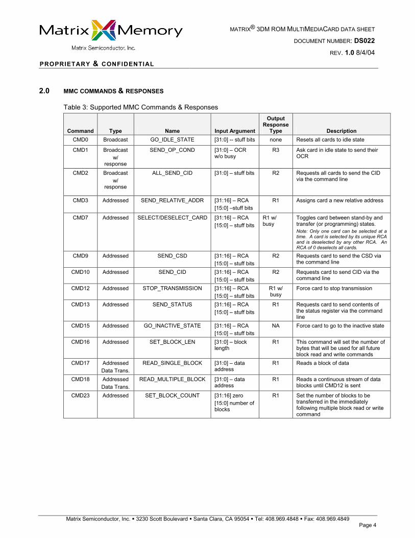
2.0 MMC COMMANDS & RESPONSES
Table 3: Supported MMC Commands & Responses
Command Type Name Input Argument
Output Response
Type Description CMD0 Broadcast GO_IDLE_STATE [31:0] -- stuff bits none Resets all cards to idle state
CMD1 Broadcast w/
response
SEND_OP_COND [31:0] – OCR w/o busy
R3 Ask card in idle state to send their OCR
CMD2 Broadcast w/
response
ALL_SEND_CID [31:0] – stuff bits R2 Requests all cards to send the CID via the command line
CMD3 Addressed SEND_RELATIVE_ADDR [31:16] – RCA [15:0] –stuff bits
R1 Assigns card a new relative address
CMD7 Addressed SELECT/DESELECT_CARD [31:16] – RCA [15:0] – stuff bits
R1 w/ busy
Toggles card between stand-by and transfer (or programming) states. Note: Only one card can be selected at a time. A card is selected by its unique RCA and is deselected by any other RCA. An RCA of 0 deselects all cards.
CMD9 Addressed SEND_CSD [31:16] – RCA [15:0] – stuff bits
R2 Requests card to send the CSD via the command line
CMD10 Addressed SEND_CID [31:16] – RCA [15:0] – stuff bits
R2 Requests card to send CID via the command line
CMD12 Addressed STOP_TRANSMISSION [31:16] – RCA [15:0] – stuff bits
R1 w/ busy
Force card to stop transmission
CMD13 Addressed SEND_STATUS [31:16] – RCA [15:0] – stuff bits
R1 Requests card to send contents of the status register via the command line
CMD15 Addressed GO_INACTIVE_STATE [31:16] – RCA [15:0] – stuff bits
NA Force card to go to the inactive state
CMD16 Addressed SET_BLOCK_LEN [31:0] – block length
R1 This command will set the number of bytes that will be used for all future block read and write commands
CMD17 Addressed Data Trans.
READ_SINGLE_BLOCK [31:0] – data address
R1 Reads a block of data
CMD18 Addressed Data Trans.
READ_MULTIPLE_BLOCK [31:0] – data address
R1 Reads a continuous stream of data blocks until CMD12 is sent
CMD23 Addressed SET_BLOCK_COUNT [31:16] zero [15:0] number of blocks
R1 Set the number of blocks to be transferred in the immediately following multiple block read or write command

PROPRIETARY & CONFIDENTIAL
MATRIX® 3DM ROM MULTIMEDIACARD DATA SHEET
DOCUMENT NUMBER: DS022
REV. 1.0 8/4/04
Matrix Semiconductor, Inc. 3230 Scott Boulevard Santa Clara, CA 95054 Tel: 408.969.4848 Fax: 408.969.4849 Page 5
Table 4: Unsupported MMC Commands
Command Type Name Input Argument
Output Response
Type Description CMD4 Broadcast SET_DSR [31:16] – DSR
[15:0] – stuff bits none Programs DSR of all cards
CMD11 Addressed Data Trans
READ_DAT_UNTIL_STOP [31:0]- data address
R1 Read data stream
CMD20 Addressed Data Trans
WRITE_DAT_UNTIL_STOP [31:0]- data address
R1 Write data stream
CMD24 Addressed Data Trans.
WRITE_BLOCK [31:0] – data address
R1 Writes a block of data
CMD25 Addressed Data Trans.
WRITE_MULTIPLE_BLOCK [31:0] – data address
R1 Writes a continuous stream of data blocks until CMD12 is sent
CMD26 Addressed Data Trans.
PROGRAM_CID [31:0] – stuff bits R1 Writes the CID, allowed once per card (normally reserved for manufacturer)
CMD27 Addressed Data Trans.
PROGRAM_CSD [31:0] – stuff bits R1 Writes to the programmable bits of the CSD
CMD28 Addressed SET_WRITE_PROT [31:0] – address bits
R1 w/busy Sets the write protect bit of the addressed group
CMD29 Addressed CLR_WRITE_PROT [31:0] – address bits
R1 w/ busy Clears the write protect bit of the addressed group
CMD30 Addressed Data Trans
SEND_WRITE_PROT [31:0] – address bits
R1 Request status of the write protection bits
CMD35 Addressed ERASE_GROUP_START [31:0] – data address
R1 Sets the address of the first erase group
CMD36 Addressed ERASE_GROUP_END [31:0] – data address
R1 Sets the address of the last erase group
CMD38 Addressed ERASE [31:0] – stuff bits R1 Erases all write blocks that were previously selected
CMD39 Addressed FAST_IO [31:16] - RCA [15:15] - reg wr flag [14:8] - Reg addr [7:0] - Reg data
R4 Used to write 8-bit reg data fields in I/O mode
CMD40 Broadcast w/response
GO_IRQ_STATE [31:0] stop F bits R5 Puts the system in interrupt mode
CMD42 Addressed Data Trans.
LOCK_UNLOCK [31:0] R1 Sets or resets the password. Or, locks or unlocks the card
CMD55 Addressed APP_CMD [31:16] – RCA [15:0] – stuff bits
R1 Preface for an application specific command
PROPRIETARY & CONFIDENTIAL
MATRIX® 3DM ROM MULTIMEDIACARD DATA SHEET
DOCUMENT NUMBER: DS022
REV. 1.0 8/4/04
Matrix Semiconductor, Inc. 3230 Scott Boulevard Santa Clara, CA 95054 Tel: 408.969.4848 Fax: 408.969.4849 Page 6
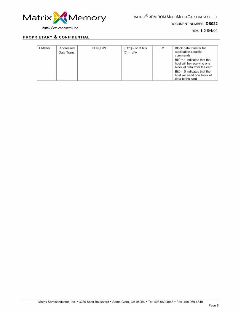
CMD56 Addressed Data Trans.
GEN_CMD [31:1] – stuff bits [0] – rd/wr
R1 Block data transfer for application specific commands. Bit0 = 1 indicates that the host will be receiving one block of data from the card Bit0 = 0 indicates that the host will send one block of data to the card

PROPRIETARY & CONFIDENTIAL
MATRIX® 3DM ROM MULTIMEDIACARD DATA SHEET
DOCUMENT NUMBER: DS022
REV. 1.0 8/4/04
Matrix Semiconductor, Inc. 3230 Scott Boulevard Santa Clara, CA 95054 Tel: 408.969.4848 Fax: 408.969.4849 Page 7
Table 5: Summary of MMC Responses
Response Width Details R1 48
Bits [47] [46] [45:40] [39:8] [7:1] [0]
Definition Start bit
Direction (indicates transmission from card)
Command index this response pertains to
Card status CRC7 end bit
Value(s) 0 0 0 to 63 (binary)
Refer to Table 13
CRC7 1
R1 w/ busy
48 Bits [47] [46] [45:40] [39:8] [7:1] [0]
Definition
Start bit
Direction (indicates transmission from card)
Command index this response pertains to
Card status CRC7 end bit
Value(s) 0 0 0 to 63 (binary)
refer to Table 13
CRC7 1
--may have a busy signal transmitted on the DAT line
R2 136 Bits [135] [134] [133:128] [127:1] [0]
Definition Start bit
Direction (indicates transmission from card)
Reserved CID or CSD register contents
end bit
Value(s) 0 0 ‘111111’ Refer to Table 10 & Table 11
1
-- the last bit of the CID and CSD registers (bit[0]) is not sent.
R3 48 Bits [47] [46] [45:40] [39:8] [7:1] [0]
Definition Start bit
Direction (indicates transmission from card)
Reserved OCR register contents
Reserved End bit
Value(s) 0 0 ‘111111’ Refer to Table 12
‘111111’ 1
PROPRIETARY & CONFIDENTIAL
MATRIX® 3DM ROM MULTIMEDIACARD DATA SHEET
DOCUMENT NUMBER: DS022
REV. 1.0 8/4/04
Matrix Semiconductor, Inc. 3230 Scott Boulevard Santa Clara, CA 95054 Tel: 408.969.4848 Fax: 408.969.4849 Page 8
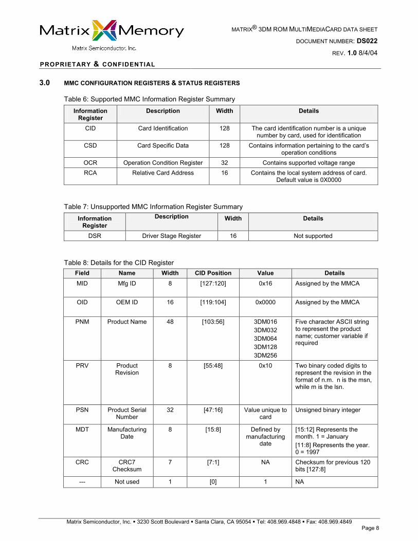
3.0 MMC CONFIGURATION REGISTERS & STATUS REGISTERS
Table 6: Supported MMC Information Register Summary
Information Register
Description Width Details
CID Card Identification 128 The card identification number is a unique number by card, used for identification
CSD Card Specific Data 128 Contains information pertaining to the card’s operation conditions
OCR Operation Condition Register 32 Contains supported voltage range RCA Relative Card Address 16 Contains the local system address of card.
Default value is 0X0000
Table 7: Unsupported MMC Information Register Summary
Information Register
Description Width Details
DSR Driver Stage Register 16 Not supported
Table 8: Details for the CID Register Field Name Width CID Position Value Details MID Mfg ID 8 [127:120] 0x16 Assigned by the MMCA
OID OEM ID 16 [119:104] 0x0000 Assigned by the MMCA
PNM Product Name 48 [103:56] 3DM016 3DM032 3DM064 3DM128 3DM256
Five character ASCII string to represent the product name; customer variable if required
PRV Product Revision
8 [55:48] 0x10 Two binary coded digits to represent the revision in the format of n.m. n is the msn, while m is the lsn.
PSN Product Serial Number
32 [47:16] Value unique to card
Unsigned binary integer
MDT Manufacturing Date
8 [15:8] Defined by manufacturing
date
[15:12] Represents the month. 1 = January [11:8] Represents the year. 0 = 1997
CRC CRC7 Checksum
7 [7:1] NA Checksum for previous 120 bits [127:8]
--- Not used 1 [0] 1 NA

PROPRIETARY & CONFIDENTIAL
MATRIX® 3DM ROM MULTIMEDIACARD DATA SHEET
DOCUMENT NUMBER: DS022
REV. 1.0 8/4/04
Matrix Semiconductor, Inc. 3230 Scott Boulevard Santa Clara, CA 95054 Tel: 408.969.4848 Fax: 408.969.4849 Page 9
Table 9: Details for the CSD Register
Field Name Width Type CSD
Position
Value Remarks CSD_STRUCTURE CSD
structure version
2 R [127:126] 0x2 0 = CSD Version 1.0 1 = CSD Version 1.1 2 = CSD Version 1.2 3 = Reserved
SPEC_VERS System spec version
4 R [125:122] 0x3 3 = Version 3.1
Reserved na 2 R [121:120] 0x0 TAAC Data read
access time-1
8 R [119:112] 0x45 2:0 = time unit 0=1ns; 1=10ns; 2=100ns; 3=1µs; 4=10µs; 5=100µs; 6=1ms; 7=10ms 6:3 = time value 0=reserved; 1=1.0; 2=1.2; 3=1.3; 4=1.5; 5=2.0; 6=2.5; 7=3.0; 8=3.5; 9=4.0; A=4.5; B=5.0; C=5.5; D=6.0; E=7.0; F=8.0 7 = reserved (NB: Represents average read access time value of 350 µs)
NSAC Data read access time-2 (in clock cycles)
8 R [111:104] 0x10 Represents the worst case for the clock dependent factor of the data access time (units = 100 clock cycles)
TRAN_SPEED Maximum data transfer rate
8 R [103:96] 0x2A 2:0 = transfer rate units 0=100kbit/s; 1=1Mbit/s; 2=10Mb/s; 3=100Mb/s; 4 to 7 =reserved 6:3 = time value 0=reserved; 1=1.0; 2=1.2; 3=1.3; 4=1.5; 5=2.0; 6=2.5; 7=3.0; 8=3.5; 9=4.0; A=4.5; B=5.0; C=5.5; D=6.0; E=7.0; F=8.0 7 = reserved
CCC Card command classes
12 R [95:84] 0x005 0:11 = Class 0 to Class 11 respectively. 1 indicates that the class is supported
READ_BL_LEN Maximum read data block length
4 R [83:80] 0x9 Read data block length is = 2READ_BL_LEN 0-8 = reserved 12-15 = reserved 9 = valid All other values are invalid

PROPRIETARY & CONFIDENTIAL
MATRIX® 3DM ROM MULTIMEDIACARD DATA SHEET
DOCUMENT NUMBER: DS022
REV. 1.0 8/4/04
Matrix Semiconductor, Inc. 3230 Scott Boulevard Santa Clara, CA 95054 Tel: 408.969.4848 Fax: 408.969.4849 Page 10
Field Name Width Type CSD
Position
Value Remarks READ_BL_PARTIAL Partial block
reads enable 1 R [79] 0x1 Always set to ‘1’ to
indicate that partial block reads are enabled.
WRITE_BLK_MISALIGN Write block misalignment
1 R [78] 0x0 Always set to ‘0’ to indicate that crossing physical block boundaries is not allowed during writes.
READ_BLK_MISALIGN Read block misalignment
1 R [77 0x0 Always set to ‘0’ to indicate that crossing physical block boundaries is not allowed during reads.
DSR_IMP DSR implemented
1 R [76] 0x0 Always set to ‘0’ to indicate that DSR is not implemented.
NA Reserved 2 na [75:74] 0x0 NA C_SIZE Device size 12 R [73:62] 0xFFE Memory capacity =
BlockNR * Block Len BlockNR = (C_Size+1)*(2C_Size_mult+2) BlockLen = 2read_bl_len
VDD_R_CURR_MIN Maximum read current @ Vdd min.
3 R [61:59] 0x6 2:0 = Idd value [A] 0=0.5m; 1=1m; 2=5m; 3=10m; 4=25m; 5=35m; 6=60m; 7=100m
VDD_R_CURR_MAX Maximum read current @ Vdd max
3 R [58:56] 0x6 2:0 = Idd value [A] 0=1m; 1=5m; 2=10m; 3=25m; 4=35m; 5=45m; 6=80m; 7=200m
VDD_W_CURR_MIN Maximum write current @ Vdd min
3 R [55:53] 0x7 2:0 = Idd value [A] 0=0.5m; 1=1m; 2=5m; 3=10m; 4=25m; 5=35m; 6=60m; 7=100m
VDD_W_CURR_MAX Maximum write current @ Vdd max
3 R [52:50] 0x7 2:0 = Idd value [A] 0=1m; 1=5m; 2=10m; 3=25m; 4=35m; 5=45m; 6=80m; 7=200m
C_SIZE_MULT Device size multiplier
3 R [49:47] 0x1 (16MB) 0x2 (32MB) 0x3 (64MB) 0x4 (128MB) 0x5 (256MB)
Value 0 to 7 used in C_SIZE calculation
ERASE_GRP_SIZE Erase group size
5 R [46:42] 0x00 This field is not applicable since erase operations are not supported.
ERASE_GRP_MULT Erase group size multiplier
5 R [41:37] 0x00 This field is not applicable since erase operations are not supported.

PROPRIETARY & CONFIDENTIAL
MATRIX® 3DM ROM MULTIMEDIACARD DATA SHEET
DOCUMENT NUMBER: DS022
REV. 1.0 8/4/04
Matrix Semiconductor, Inc. 3230 Scott Boulevard Santa Clara, CA 95054 Tel: 408.969.4848 Fax: 408.969.4849 Page 11
Field Name Width Type CSD
Position
Value Remarks WP_GRP_SIZE Write protect
group size 5 R [36:32] 0x00 This field is not
applicable since erase operations are not supported.
WP_GRP_ENABLE Write protect group enable
1 R [31] 0x0 Always set to ‘0’ to indicate that no group write protection is possible.
DEFAULT_ECC Manufacturer default ECC
2 R [30:29] 0x0 Manufacturer recommended ECC type to use: Always ‘0’ indicating no external ECC required.
R2W_FACTOR Write speed factor
3 R [28:26] 0x1 Block program time in terms of block read time 0 = 1 (wr time = rd time); 1 = 2 (wr time = 2 * rd time); 2 = 4; 3 = 8; 4 = 16; 5 = 32; 6&7 = reserved.
WRITE_BL_LEN Maximum write data block length
4 R [25:22] 0x9 Write data block length is = 2WRITE_BL_LEN 0-8 = reserved 12-15 = reserved 9 = valid all other values are invalid
WRITE_BL_PARTIAL Partial block write enable
1 R [21] 0x0 Always set to ‘0’ to indicate that partial block writes are disabled.
Reserved na 5 R [20:16] 0x00 FILE_FORMAT_GRP File format
group 1 R [15] 0x0 Indicates the selected
group of file formats (read only) 0 = valid 1 = reserved
COPY Copy flag 1 R [14] 0x0 Content is original PERM_WRITE_PROTECT Permanent
write protect 1 R [13] 0x1 At startup will be
asserted to protect the card from non-enabled systems. After the ID_3DM command is completed it will be deasserted. The card can also be permanently protected by setting the bit explicitly.

PROPRIETARY & CONFIDENTIAL
MATRIX® 3DM ROM MULTIMEDIACARD DATA SHEET
DOCUMENT NUMBER: DS022
REV. 1.0 8/4/04
Matrix Semiconductor, Inc. 3230 Scott Boulevard Santa Clara, CA 95054 Tel: 408.969.4848 Fax: 408.969.4849 Page 12
Field Name Width Type CSD
Position
Value Remarks TMP_WRITE_PROTECT Temporary
write protect 1 R [12] 0x1 Temporarily write
protects the card. At startup will be asserted to protect the card from non-enabled systems. After the ID_3DM command is completed it will be deasserted.
FILE_FORMAT File format 2 R [11:10] 0x0 Indicates the format of the card. Valid if FORMAT_GROUP is 0: 0 = “hard disk” partition table 1 = “DOS FAT” 2 = universal file format 3 = others / unknown
ECC ECC code 2 R [9:8] 0x0 ECC used to decode user data 0=none (default) 1=BCH (542, 512) 3 correctable Bits 2-3=reserved
CRC CRC7 checksum
7 R [7:1] NA Checksum for previous 120 bits
Reserved NA 1 R [0] 0x1 Not used, always reads as a ‘1’
PROPRIETARY & CONFIDENTIAL
MATRIX® 3DM ROM MULTIMEDIACARD DATA SHEET
DOCUMENT NUMBER: DS022
REV. 1.0 8/4/04
Matrix Semiconductor, Inc. 3230 Scott Boulevard Santa Clara, CA 95054 Tel: 408.969.4848 Fax: 408.969.4849 Page 13
Table 10: OCR Bit Definition OCR Bit VDD Window Value
0 1.45-1.50 0 1 1.50 – 1.55 0 2 1.55-1.60 0 3 1.60-1.65 0 4 1.65 – 1.70 0 5 1.7 – 1.8 0 6 1.8 – 1.9 0 7 1.9 – 2.0 0 8 2.0 – 2.1 0 9 2.1 – 2.2 0
10 2.2 – 2.3 0 11 2.3 – 2.4 0 12 2.4 – 2.5 0 13 2.5 – 2.6 0 14 2.6 – 2.7 0
15 2.7 – 2.8 1 16 2.8 – 2.9 1 17 2.9 – 3.0 1 18 3.0 – 3.1 1 19 3.1 – 3.2 1 20 3.2 – 3.3 1 21 3.3 – 3.4 1 22 3.4 – 3.5 1 23 3.5 – 3.6 1
24-30 NA 0 31 NA Power-Up status. Bit is low till the
part has completed the power up routine.

PROPRIETARY & CONFIDENTIAL
MATRIX® 3DM ROM MULTIMEDIACARD DATA SHEET
DOCUMENT NUMBER: DS022
REV. 1.0 8/4/04
Matrix Semiconductor, Inc. 3230 Scott Boulevard Santa Clara, CA 95054 Tel: 408.969.4848 Fax: 408.969.4849 Page 14
Table 11: MMC Status Field Details Bit Name Description Value Type Set Cleared 31 OUT_OF_RANGE Address was out of
range 0 = no error 1 = error
Error Response & execution
Read
30 ADDRESS_ERROR Addressed block was misaligned
0 = no error 1 = error
Error Response Read
29 BLOCK_LEN_ERROR Invalid block length 0 = no error 1 = error
Error Response Read
28 ERASE_SEQ_ERROR Erase sequencing error 0 = no error 1 = NA
Error Response Read
27 ERASE_PARAM Invalid write block selection during erase
0 = no error 1 = NA
Error Response & execution
Read
26 WP_VIOLATION Attempted to write a protected block
0 = no error 1 = error
Error Response & execution
Read
25 CARD_IS_LOCKED Locked by host 0 = not locked 1 = NA
Status Execution State
24 LOCK_UNLOCK_FAILED Invalid password or locked
0 = no error 1 = NA
Error Response & execution
Read
23 COM_CRC_ERROR CRC check for the previous command failed
0 = no error 1 = error
Error Response Valid cmd
22 ILLEGAL_COMMAND Illegal command for current state
0 = no error 1 = error
Error Response Valid cmd
21 CARD_ECC_FAILED Uncorrectable ECC fault has occurred
0 = no error 1 = error
Error Response & execution
Read
20 CC_ERROR Internal controller error 0 = no error 1 = NA
Error Response & execution
Read
19 ERROR Unknown or general error
0 = no error 1 = error
Error Response & execution
Read
18 UNDERRUN Data lost during stream read mode
0 = no error 1 = NA
Error Execution Read
17 OVERRUN Data lost during stream write mode
0 = no error 1 = NA
Error Execution read
16 CID/CSD_OVERWRITE CID already written; CSD does not match card content; or, attempted to reverse the copy or WP bits
0 = no error 1 = error
Error Response & execution
Read
15 WP_ERASE_SKIP Partial address erased due to write protect blocks
0 = not protected 1 = NA
Status Execution Read
14 CARD_ECC_DISABLED Internal ECC was off during command execution
0 = NA 1 = Default
Status Execution State
13 ERASE_RESET an erase sequence was cleared before executing due to an erase sequence command
0 = cleared 1 = NA
Status Response Read

PROPRIETARY & CONFIDENTIAL
MATRIX® 3DM ROM MULTIMEDIACARD DATA SHEET
DOCUMENT NUMBER: DS022
REV. 1.0 8/4/04
Matrix Semiconductor, Inc. 3230 Scott Boulevard Santa Clara, CA 95054 Tel: 408.969.4848 Fax: 408.969.4849 Page 15
Bit Name Description Value Type Set Cleared 12:9 CURRENT_STATE Reflects the state of
the card when the command was received.
0 = idle 1 = ready 2 = identification 3 = standby 4 = transfer 5 = send data 6 = rcv data 7 = program 8 =disconnect 9-15 = reserved
Status Execution Valid cmd
8 READY_FOR_DATA Corresponds to buffer empty signaling on the bus
0 = not ready 1 = ready
Status Execution State
7:6 Reserved 5 APP_CMD An application
command has been received, or the card is ready to receive an application command
0 = disabled 1 = enabled
Status Response Read
4:0 Reserved

PROPRIETARY & CONFIDENTIAL
MATRIX® 3DM ROM MULTIMEDIACARD DATA SHEET
DOCUMENT NUMBER: DS022
REV. 1.0 8/4/04
Matrix Semiconductor, Inc. 3230 Scott Boulevard Santa Clara, CA 95054 Tel: 408.969.4848 Fax: 408.969.4849 Page 16
4.0 SPI COMMANDS & RESPONSES
Table 12: Supported SPI Commands
Command Name Input
Argument
Output Response
Type Description CMD0 GO_IDLE_STATE None R1 Resets all cards to idle state
CMD1 SEND_OP_CONDITION None R1 Activates the cards initialization processes
CMD9 SEND_CSD None R1 Requests card to send the CSD
CMD10 SEND_CID None R1 Requests card to send CID
CMD12 STOP_TRANSMISSION None R1 w/ busy
Force card to stop transmission during multiple block read
CMD13 SEND_STATUS None R2 Requests card to send contents of the status register
CMD16 SET_BLOCK_LEN [31:0] – block length
R1 This command will set the number of bytes that will be used for all future block read and write commands.
CMD17 READ_SINGLE_BLOCK [31:0] – data address
R1 Reads a block of data.
CMD18 READ_MULTIPLE_BLOCK [31:0] – data address
R1 Reads a continuous stream of data blocks until CMD12 is sent
CMD23 SET_BLOCK_COUNT [31:16] zero [15:0] number of blocks
R1 Sets the number of blocks to be transferred in the immediately following multiple block read and write command
CMD58 READ_OCR None R3 Requests the card to send the contents of the OCR Register
CMD59 CRC_ON_OFF [31:1] – stuff bits [0]: CRC option
R1 Bit 0: 1 = CRC on 0 = CRC off Default is off

PROPRIETARY & CONFIDENTIAL
MATRIX® 3DM ROM MULTIMEDIACARD DATA SHEET
DOCUMENT NUMBER: DS022
REV. 1.0 8/4/04
Matrix Semiconductor, Inc. 3230 Scott Boulevard Santa Clara, CA 95054 Tel: 408.969.4848 Fax: 408.969.4849 Page 17
Table 13: Unsupported SPI Commands
Command Name Input
Argument
Output Response
Type Description CMD24 WRITE_BLOCK [31:0] – data
address R1 Writes a block of data
CMD25 WRITE_MULTIPLE_BLOCK [31:0] – data address
R1 Writes a continuous stream of data blocks until “Stop Tran” token is sent instead of “Start Block” token
CMD27 PROGRAM_CSD None R1 Write the programmable bits of the CSD
CMD28 SET_WRITE_PROT [31:0] – Address bits
R1 w/ busy Sets the write protect bit of the addressed group
CMD29 CLR_WRITE_PROT [31:0] – Address bits
R1 w/ busy Clears the write protect bit of the addressed group
CMD30 SEND_WRITE_PROT [31:0] – write protect data address
R1 Request status of the write protection bits
CMD38 ERASE [31:0] – stuff bits R1 w/busy Erases all write blocks that were previously selected
CMD42 LOCK_UNLOCK [31:0] R1 w/busy Sets or resets the password. Or, locks or unlocks the card
CMD55 APP_CMD [31:0] – stuff bits R1 Preface for an application specific command
CMD56 GEN_CMD [31:1] – stuff bits [0] – rd/wrn
R1 Block data transfer for application specific commands. Bit0 = 1 indicates that the host will be receiving one block of data from the card Bit0 = 0 indicates that the host will send one block of data to the card

PROPRIETARY & CONFIDENTIAL
MATRIX® 3DM ROM MULTIMEDIACARD DATA SHEET
DOCUMENT NUMBER: DS022
REV. 1.0 8/4/04
Matrix Semiconductor, Inc. 3230 Scott Boulevard Santa Clara, CA 95054 Tel: 408.969.4848 Fax: 408.969.4849 Page 18
Table 14: Summary of SPI Responses Response Width Details
R1 8
Bits Name “1” “0”
7 NA This bit is always ‘0’
6 Parameter Error The command parameter was out of range
No error
5 Address Error The addressed block was misaligned.
No error
4 Erase Sequence Error
NA This bit is always ‘0’
3 Com CRC Error The command CRC check failed
No error
2 Illegal Command The last command was invalid
No error
1 Erase Reset NA This bit is always ‘0’
0 Idle State Card is in idle and performing the initializing process
Card is not in idle state
R1 w/ busy 8
Bits Name “1” “0” 7 NA This bit is always ‘0’
6 Parameter Error The command parameter was out of range
No error
5 Address Error The addressed block was misaligned
No error
4 Erase Sequence Error
NA This bit is always ‘0’
3 Com CRC Error The command CRC check failed
No error
2 Illegal Command The last command was invalid
No error
1 Erase Reset NA This bit is always ‘0’
0 Idle State Card is in idle and performing the initializing processes
--may have a busy signal transmitted on the DO line

PROPRIETARY & CONFIDENTIAL
MATRIX® 3DM ROM MULTIMEDIACARD DATA SHEET
DOCUMENT NUMBER: DS022
REV. 1.0 8/4/04
Matrix Semiconductor, Inc. 3230 Scott Boulevard Santa Clara, CA 95054 Tel: 408.969.4848 Fax: 408.969.4849 Page 19
Response Width Details R2 16
Bits Name “1” “0”
15 NA This bit is always ‘0’
14 Parameter Error The command parameter was out of range
no error
13 Address Error The addressed block was misaligned no error
12 Erase Sequence Error
NA This bit is always ‘0’
11 Com CRC Error The command CRC check failed no error
10 Illegal Command The last command was invalid no error
9 Erase Reset NA This bit is always ‘0’
8 Idle State Card is in idle and performing the initializing process
Not in idle state
7 Out of Range / CSD Overwrite
Block does not exist or CSD overwrite error
no error
6 Erase Parameter NA This bit is always ‘0’
5 WP Violation See Table 17 This bit is always ‘0’
4 Card ECC Failure Internal ECC could not correct errors no error
3 CC Error General, internal, controller error no error
2 Error General, internal, error no error
1 WP Erase Skip NA This bit is always ‘0’
0 Card Locked NA This bit is always ‘0’ R3 40
Bits Name “1” “0” 39 NA This bit is always ‘0’
38 Parameter Error The command parameter was out of range
no error
37 Address Error The addressed block was misaligned no error
36 Erase Sequence Error
NA This bit is always ‘0’
35 Com CRC Error The command CRC check failed no error
34 Illegal Command The last command was invalid no error
33 Erase Reset NA This bit is always ‘0’
32 Idle State Card is in idle and performing the initializing process
Not in idle state
[31:0] OCR Bits [31:0] contain the contents of the OCR register
PROPRIETARY & CONFIDENTIAL
MATRIX® 3DM ROM MULTIMEDIACARD DATA SHEET
DOCUMENT NUMBER: DS022
REV. 1.0 8/4/04
Matrix Semiconductor, Inc. 3230 Scott Boulevard Santa Clara, CA 95054 Tel: 408.969.4848 Fax: 408.969.4849 Page 20
Table 15: Summary of SPI Data Tokens Token Width Details
Data Response
8
Bits Name “1” “0”
7 Not used This bit is always ‘1’ NA 6 Not used This bit is always ‘1’ NA 5 Not used This bit is always ‘1’ NA 4 NA This bit is always ‘0’ 3 2 1
Status Status: 010 = data accepted 101 = CRC error – data rejected 110 = write error – data rejected
0 NA This bit is always ‘0’
Data — single block read, multiple block read
4 to 515
bytes
Byte Name Contents
1st Start Block “11111110” 2nd to 513th User Data Data Last two CRC 16 bit CRC
(assuming a block length of 512 bytes) Note that blocks written to the card must be 512 bytes long.
Data Error 8 Bits Name “1” “0”
7 Not Used
NA This bit is always ‘0’
6 Not Used
NA This bit is always ‘0’
5 Not Used
NA This bit is always ‘0’
4 Not Used
NA This bit is always ‘0’
3 Out of Range
Block does not exist No Error
2 Card ECC Failure
Internal ECC could not correct data error
No Error
1 CC Error General, internal, controller error
No Error
0 Error General, internal error No Error

PROPRIETARY & CONFIDENTIAL
MATRIX® 3DM ROM MULTIMEDIACARD DATA SHEET
DOCUMENT NUMBER: DS022
REV. 1.0 8/4/04
Matrix Semiconductor, Inc. 3230 Scott Boulevard Santa Clara, CA 95054 Tel: 408.969.4848 Fax: 408.969.4849 Page 21
Table 16: SPI Status Field Details Name Description Value Type Set Cleared
Out of range The addressed block does not exist
0 = no error 1 = error
Error Response & Execution
Read
Address error The addressed block is misaligned
0 = no error 1 = error
Error Response & Execution
Read
Erase sequence error
NA 0 = no error Error Response Read
Erase parameter error
NA 0 = no error Error Response Read
Parameter error The command parameter was out of range
0 = no error 1 = error
Error Response & Execution
Read
WP violation Attempted to write protected block
0 = no error 1 = error
Error Response & Execution
Read
Com CRC error CRC for previous command failed
0 = no error 1 = error
Error Response Read
Illegal command Invalid command 0 = no error 1 = error
Error Response Read
Card ECC failure Internal ECC failed to correct data errors
0 = no error 1 = error
Error Execution Read
CC error General, internal, controller failure
0 = no error 1 = error
Error Response & Execution
Read
Error General, internal error 0 = no error 1 = error
Error Response & Execution
Read
WP erase skip NA 0 = not protected Status Execution Read CSD Overwrite Attempt to write ROM
section of the CSD, change copy bit, or change write protect bit
0 = no error 1 = error
Error Response & execution
Read
Lock/unlock cmd failure
NA 0 = no error
Error Execution Read
Card is locked NA 0 = not locked Status Execution State Erase reset NA 0 = not cleared Status Response Read In idle state Currently in idle state and
performing initialization process
0 = ready 1 = idle state
Status Response State

PROPRIETARY & CONFIDENTIAL
MATRIX® 3DM ROM MULTIMEDIACARD DATA SHEET
DOCUMENT NUMBER: DS022
REV. 1.0 8/4/04
Matrix Semiconductor, Inc. 3230 Scott Boulevard Santa Clara, CA 95054 Tel: 408.969.4848 Fax: 408.969.4849 Page 22
5.0 SPI CONFIGURATION REGISTERS & STATUS REGISTERS
Any SPI variations from standard MMC register values are discussed in Section 3. 6.0 MMC AC SPECIFICATIONS
Table 17: MMC AC Specifications Symbol Parameter Min Max Remarks
Tper_op Input clock period after identification mode 50 ns 5µs CL ≤ 100pF
(10 cards)
Tper_poll Input clock period after identification mode (open drain)
2.5µs 10µs
Tlo 1 Input clock low time 50ns --- CL ≤ 250pF
Thi 1 Input clock hi time 50ns --- CL ≤ 250pF
Tlo 2 Input clock low time 10ns CL ≤ 100pF
Thi 2 Input clock hi time 10ns CL ≤ 100pF
Tis Input set up time 3ns ---
Tih Input hold time 3ns ---
Tos Output set up time 5ns
Toh Output hold time 5ns
Tlo2hi 1 Clock rise time 50ns CL ≤ 250pF
Thi2low 1 Clock fall time 50ns CL ≤ 250pF
Tlo2hi 2 Clock rise time 10ns CL ≤ 100pF
Thi2low 2 Clock fall time 10ns CL ≤ 100pF
Note: The MMC card is negative edge triggered
ToutTout
TihTis
Tper
ThiThiTlo
Tper
TloClock
Input: CMD, DAT
Output: CMD, DAT
Figure 1: AC Specifications

PROPRIETARY & CONFIDENTIAL
MATRIX® 3DM ROM MULTIMEDIACARD DATA SHEET
DOCUMENT NUMBER: DS022
REV. 1.0 8/4/04
Matrix Semiconductor, Inc. 3230 Scott Boulevard Santa Clara, CA 95054 Tel: 408.969.4848 Fax: 408.969.4849 Page 23
7.0 MMC TIMING SPECIFICATIONS
Table 18: MMC Timing Specifications Symbol Parameter Min Max
NCR Host command to card response delay 2 clks 64 clks NID Identification delay 5 clks 5 clks NAC Data access delay 2 clks TAAC+NSAC NRC Card response to next host command delay 8 clks ---- NCC Host command to next host command delay 8 clks ----
TAAC Data transfer delay due to memory 320µs NSAC Data transfer delay due to controller 100 clks 1600 clks
Table 19: MMC/CMD2/CMD1 Timing Specifications (Open drain mode) Host on Command Bus Card on Command Bus
Start Bit
Trans. Bit
Command CRC End Bit
NID Start Bit
Trans. Bit
Response
0 1 CMD2 or CMD1
CRC 1 Z Z Z … Z 0 0 CID or OCR
Z Z
Table 20: MMC CMD3 Timing Specifications (Open drain mode) Host on Command Bus Card on Command Bus
Start Bit
Trans. Bit
Command CRC End Bit
NCR Start Bit
Trans. Bit
Response
0 1 CMD3 CRC 1 Z Z Z … Z 0 0 Content Z Z
Table 21: MMC All Data Transfer Commands Timing Specifications Host on Command Bus Card on bus
Start Bit
Trans. Bit Command CRC End Bit
NCR Start Bit
Trans. Bit
Response
0 1 Content CRC 1 Z Z P … P 0 0 Content Z Z
Table 22: MMC Response to Next Command During Data Transfer Timing Specifications Card on Command Bus Card on Command
Bus
Start Bit
Trans. Bit
Prev. Response
CRC End Bit
NRC Start Bit
Trans Bit
Command CRC End Bit
0 0 CONTENT CRC 1 Z … Z 0 1 Content CRC 1 Z Z

PROPRIETARY & CONFIDENTIAL
MATRIX® 3DM ROM MULTIMEDIACARD DATA SHEET
DOCUMENT NUMBER: DS022
REV. 1.0 8/4/04
Matrix Semiconductor, Inc. 3230 Scott Boulevard Santa Clara, CA 95054 Tel: 408.969.4848 Fax: 408.969.4849 Page 24
Table 23: MMC Command to Next Command Timing Specifications Host on Command Bus Host on Command Bus
Start Bit
Trans. Bit
Prev. Command
CRC End Bit
NCC Start Bit
Trans Bit
Command CRC End Bit
0 1 CONTENT CRC 1 Z … Z 0 1 Content CRC 1 Z Z
Table 24: MMC Block Read Timing Specifications Host on Command Bus Card on Command Bus
Start Bit
Trans. Bit
Command CRC End Bit NCR Start Bit
Trans. Bit
Response
0 1 CMD17 CRC 1 Z Z P … P 0 0 Content Z Z Card on Data Bus
Data Bus Tristated NAC Cycles Valid Data Z … Z Z Z Z P … P 0 D …
Table 25: MMC Read Multiple Block Timing Specifications (Initial Block)
Host on Command Bus Card on Command Bus Start Bit
Trans.Bit
Command CRC End Bit
NCR Start Bit
Trans. Bit
Response
0 1 CMD18 CRC 1 Z Z P … P 0 0 Content Z Z Card on Data Bus
Data Bus Tristated NAC Cycles Valid Data Z … Z Z Z Z P … P 0 D …
Table 26: MMC Read Multiple Block Timing Specifications (Following Blocks) Card on Command Bus Card on Command Bus
P ... PCard on Data Bus
Previous Read NAC Valid Data D … D CRC 1 P … P 0 D …
Table 27: MMC Read Multiple Block Timing Specifications (Stop Command) Host on Command Bus Card on Command Bus
Start Bit
Trans. Bit
Command CRC End Bit
NCR Start Bit
Trans. Bit
Response
0 1 CMD12 CRC 1 Z Z P … P 0 0 Content Z Z Card on Data Bus
Last Read NST D … D D D D 1 Z … Z Z Z …
NOTE: The stop command may be issued during the transmission of a data packet. It is not a requirement that the stop command be
issued after the end bit of the “previous read.”

PROPRIETARY & CONFIDENTIAL
MATRIX® 3DM ROM MULTIMEDIACARD DATA SHEET
DOCUMENT NUMBER: DS022
REV. 1.0 8/4/04
Matrix Semiconductor, Inc. 3230 Scott Boulevard Santa Clara, CA 95054 Tel: 408.969.4848 Fax: 408.969.4849 Page 25
8.0 SPI AC SPECIFICATIONS SUMMARY
The SPI AC specifications are the same as the MMC specifications.
9.0 SPI TIMING SPECIFICATIONS
Table 28: SPI Timing Specifications
Symbol Parameter Min Max NCS Card select to card ready 0 clks -- NCR Host command to card ready 8 clks 64 clks NRC Card response to next command 8 clks -- NAC Data access delay 8 clks In CSD NEC Busy time after response 0 clks -- NDS Card deselect to data out inhibit 0 clks -- NCX CSD read data delay 0 clks 64 clks

PROPRIETARY & CONFIDENTIAL
MATRIX® 3DM ROM MULTIMEDIACARD DATA SHEET
DOCUMENT NUMBER: DS022
REV. 1.0 8/4/04
Matrix Semiconductor, Inc. 3230 Scott Boulevard Santa Clara, CA 95054 Tel: 408.969.4848 Fax: 408.969.4849 Page 26
Table 29: Host Command to Card Response (card is ready) CS
H H L L L … L L L L H H H …
Data In
NCS NEC
X X H H H H Command: 6 bytes H H H H H …
Data Out
NCR
Z Z Z H H H H … H H H H H Response: 1 or 2 Bytes H H H H H Z Z …
Table 30: Host Command to Card Response (card is busy) CS
H H L L L … L L H H
Data In
NCS NEC NDS NEC
X X H H H H Command: 6 bytes H H H H H H H H H H H H H X X X H H H H H H H H H X …
Data Out
NCR
Z Z Z H H H … H H H H H Response Busy L Z Z Z Busy H H H H Z …
Table 31: Card Response to Host Command CS
L L L L L … L L H H H Data In
H H H H H H H H Command: 6 bytes H H H H X X X … Data Out
NRC
H H H H H Response: 1 or 2 byte H H H H H H H H H Z Z …
Table 32: Data Read (Single block or start of multiple block) CS
H L L L L … L L L H H H H …
Data In NCS NEC
X H H H H Read Cmd H H H H H … H H H H X X X X …
Data Out NCR NAC
Z Z H H H H … H H H H Card response H H H H Data Transfer H H H H Z Z Z …

PROPRIETARY & CONFIDENTIAL
MATRIX® 3DM ROM MULTIMEDIACARD DATA SHEET
DOCUMENT NUMBER: DS022
REV. 1.0 8/4/04
Matrix Semiconductor, Inc. 3230 Scott Boulevard Santa Clara, CA 95054 Tel: 408.969.4848 Fax: 408.969.4849 Page 27
Table 33: Termination of Multiple Block Read CS
L L L L …
Data In
X H H H H Stop Transmission Cmd H H H H H …
Data Out
NCR Data Transfer X X H … H Card Response H H …
Table 34: CSD Register Read CS
H L L L … L L L L H H HData In
NCS NEC
X H H H H Read CSD Cmd H H H H H … H H H H X X XData Out
NCR NCx
Z Z H H H H … H H H H H Card Response H H H H Data Transfer H H H H Z Z

PROPRIETARY & CONFIDENTIAL
MATRIX® 3DM ROM MULTIMEDIACARD DATA SHEET
DOCUMENT NUMBER: DS022
REV. 1.0 8/4/04
Matrix Semiconductor, Inc. 3230 Scott Boulevard Santa Clara, CA 95054 Tel: 408.969.4848 Fax: 408.969.4849 Page 28
10.0 POWER AND I/O SPECIFICATIONS
Table 35: Absolute Maximum Specifications Symbol Parameter Min Max Toper Operating Temp 0ºC 60°C Tstore Storage Temp -25°C 85°C
C(1) Pin capacitance -- 10pF VDDmax Maximum applied VDD -0.30 V 4.50 V VINmax Maximum applied input voltage -0.50 V VDD+ 0.50V
Table 36: Operating Voltage and Current Specifications Symbol Parameter Min Typ Max
VDD Operating voltage 2.70 V -- 3.60 V VDDPOR Device initialization voltage (see page 27) 2.00 V -- 3.60 V VDDdif Operating voltage differential -0.30 V -- +0.30 V IDDR Operating read current -- 30 mA 45 mA
VINMAX Maximum applied input voltage -0.50 V -- VDD + 0.50 V IDDQ1 Standby current for 16, 32 and 64MB cards -- 100 µA 200 µA IDDQ2 Standby current for 128MB card -- 150 µA 300 µA IDDQ3 Standby current for 256MB card -- 250 µA 500 µA
Note: Standby current measured in STBY state
Table 37: Input/Output Leakage Specifications Symbol Parameter Min Max
IL Input leakage current (Vih = VDD or Vil = GND)
-10 µA 10 µA
IOZ Tristate leakage (Gnd or VDD) -10 µA 10 µA
Table 38: Input/Output Level Specifications Symbol Parameter Min Max
Vih Input high voltage 3.3V operation 0.625 * VDD Vcc + 0.30 V Vil Input low voltage 3.3V operation -0.30 V 0.25 * VDD
Voh Output high voltage (Ioh = -100 uA) 0.75 * VDD -- Vol Output low voltage (Iol = 100 uA) -- 0.125 * VDD
II Maximum input current -10 µA 10 µA
Table 39: Pin 1 Pullup Resistor Specification Symbol Parameter Min Max
RPU Pull up resistor (on pin 1 only) 10 kΩ 90 kΩ

PROPRIETARY & CONFIDENTIAL
MATRIX® 3DM ROM MULTIMEDIACARD DATA SHEET
DOCUMENT NUMBER: DS022
REV. 1.0 8/4/04
Matrix Semiconductor, Inc. 3230 Scott Boulevard Santa C
11.0 POWER-ON RESET SPECIFICATIONS
Figure 2: Pow
NOTE: During boot up in the SPI mode, the host mubefore examining the content of the OCR regcard (CMD1) before reading the OCR (CMD5compatible with the range that the host will sup
VDDpor
All commands valid after initialization, Voltage Range: VDD MIN to VDDMAX
VDDmax
VDDmin
TIME
Only CMD0 and CMD1 may beapplied during MMC mode. Only CMD0 and CMD58 may be applied during SPI mode. Max of 1m Sec, 74 clks and supply ramp, Voltage Range: VDDpor to VDDmax
lara, CA 95054 Tel: 408.969.4848 Fax: 408.969.4849 Page 29
er-on Reset Specification
st not issue any commands other than CMD0 and CMD58 ister. In other words, the host must not attempt to boot the 8) and making sure that the card's supply voltage range is ply.