MATERIALS PHYSICS AND MECHANICS
75
ISSN 1605-2730 MATERIALS PHYSICS AND MECHANICS Vol. 1, No. 1, 2000
Transcript of MATERIALS PHYSICS AND MECHANICS

ISSN 1605-2730
MATERIALS PHYSICS AND
MECHANICS
Vol. 1, No. 1, 2000
MATERIALS PHYSICS AND MECHANICS
PRINCIPAL EDITORS V. P. Bulatov
Institute of Problems
of Mechanical Engineering
(Russian Academy of Sciences(RAS))
EDITORIAL STAFF I. Yu. Archakov, Staff Editor
A. B. Reizis, Production Editor
EDITORIAL BOARD Y. G. Gogotsi University of Illinois
at Chicago, USA
S. A. Kukushkin Institute of Problems of Mechanical Engineering (RAS)
I. A. Ovid'ko
Institute of Problems of Mechanical Engineering
(Russian Academy of Sciences (RAS))
V. F. Stepanets, Production Editor
A. E. Romanov Joffe Physico-Technical Institute (RAS)
Y. F. Titovets St. Petersburg State Technical University, Russia A. Tholen Chalmers Laboratory, Sweden
Editorial Office:
Materials Physics and Mechanics Editorial Office
Institute of Problems of Mechanical Engineering (Russian Academy of Sciences), Bolshoi 61, Vas. Ostrov, St. Petersburg 199178, Russia
FAX+7(812)3214771 E-mail :[email protected]
Web-sites: http://www,ipme.ru/e-iournals/MPM/ httpV/www.ipme.nw.ru/e-iournals/MPM/
http://mclab.me.uic.edu/MPM
Materials Physics and Mechanics (ISSN 1605-2730) - Published quarterly, one volume per year, by Advanced Study Center Co. Ltd. (St.Petersburg, Russia)
Editorial Policy. The journal specializes in the rapid publication of international conference proceedings in every area of materials physics and mechanics.This permits such proceedings to be conveniently referenced, abstracted and read. All contributions are edited by the corresponding guest editor(s) and they may not be published elsewhere.The journal will cover research activities in physics and mechanics of the traditional as well as the newly emerging materials.
Owner Organizations: Institute of Problems of Mechanical Engineering Advanced Study Center Co. Ltd. (Russian Academy of Sciences, St.Petersburg, Russia) (St.Petersburg, Russia)
m

Materials Physics and Mechanics
Volume 1, Number 1, March 2000
100 Yft
AD foi- n-^aii
Editorial Policy. The journal specializes in the rapid publication of international conference proceedings in every area of materials physics and mechanics.This permits such proceedings to be conveniently referenced, abstracted and read. All contributions are edited by the corresponding guest editor(s) and they may not be published elsewhere.The journal will cover research activities in physics and mechanics of the traditional as well as the newly emerging materials.
© Advanced Study Co. Ltd., (Saint-Petersburg, Russia), 2000

International Workshop on APPLIED ASPECTS OF INTERFACE SCIENCE (AAIS)
(St.Petersburg, Russia; September 22 - 24, 1999)
Sponsored by
US Office of Naval Research, International Field Offtee, Europe
European Office of Aerospace Research and Development, UK
European Research Office of the US Army, UK
Announcement:
If any one technology can be said to shape the face of today society, it is materials technology. New materials, materials processes and applications are of major importance in boosting other military and civilian technological sectors such as electronics, energy technology and aerospace engineering. The objective of this Workshop is to present current research on advanced nanostructured materials and high temperature superperconducting materials (characterized by nano-scaled coherence length) with the special attention being paid to the effect of interfaces on the unique, commonly highly desired properties of such materials as well their applications in various high technology areas. The Workshop aims to assess the current status and to identify future directions of R&D and applications of nanostructured bulk solids, films and coatings as well as polycrystalline superconducting materials. Particular emphasis is placed on developing close interactions and fostering future collaborations among scientists and engineers from the USA, Russia and other countries.
We plan to focus to the following topics Synthesis and processing; Modeling; Characterization and properties (mechanical and transport properties of nanostructured materials, high- and low-current properties of superconducting materials); Applications.
Workshop venue: Palace of Scientists, St.Petersburg, Russia
International Organizing Committee:
RMasumura (Naval Research Laboratory, USA) I.Ovid'ko (Russian Academy of Sciences, Russia) C.Pande (Naval Research Laboratory, USA) B.Smirnov (Russian Academy of Sciences, Russia) M.Soto (Office of the US Naval Research, USA)
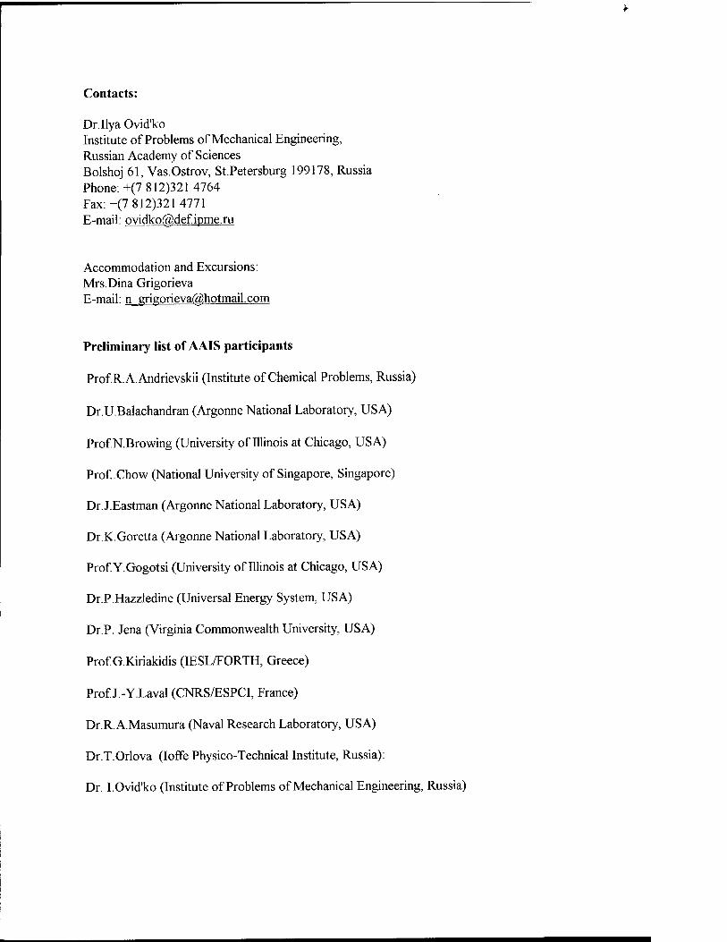
Contacts:
Dr.Ilya Ovid'ko Institute of Problems of Mechanical Engineering, Russian Academy of Sciences Bolshoj 61, Vas.Ostrov, St.Petersburg 199178, Russia Phone:+(7 812)321 4764 Fax: +(7 812)321 4771 E-mail: [email protected]
Accommodation and Excursions: Mrs.Dina Grigorieva E-mail: [email protected]
Preliminary list of AAIS participants
Prof.R.A.Andrievskii (Institute of Chemical Problems, Russia)
Dr.U.Balachandran (Argonne National Laboratory, USA)
Prof.N.Browing (University of Illinois at Chicago, USA)
Prof .Chow (National University of Singapore, Singapore)
Dr.J.Eastman (Argonne National Laboratory, USA)
Dr.K.Goretta (Argonne National Laboratory, USA)
Prof.Y.Gogotsi (University of Illinois at Chicago, USA)
Dr.P.Hazzledine (Universal Energy System, USA)
Dr.P. Jena (Virginia Commonwealth University, USA)
Prof.G.Kiriakidis (IESL/FORTH, Greece)
Prof.J.-Y.Laval (CNRS/ESPCI, France)
Dr.R. A.Masumura (Naval Research Laboratory, USA)
Dr.T.Orlova (Ioffe Physico-Technical Institute, Russia):
Dr. I.Ovid'ko (Institute of Problems of Mechanical Engineering, Russia)
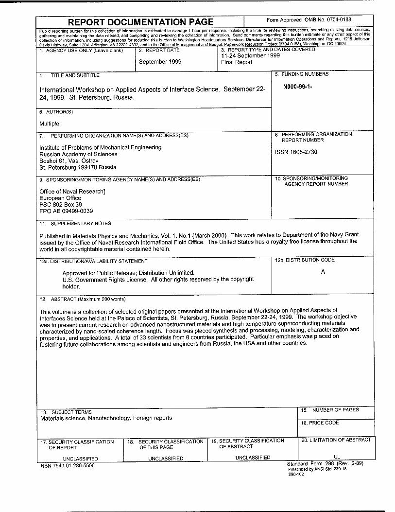
REPORT DOCUMENTATION PAGE Form Approved OMB No. 0704-0188
Public reporting burden for this collection of information is estimated to average 1 hour per response, including the time for reviewing instructions, searching existing data sources, gathering and maintaining the data needed, and completing and reviewing the collection of information. Send comments regarding this burden estimate or any other aspect of this collection of information, including suggestions for reducing this burden to Washington Headquarters Services, Directorate for Information Operations and Reports, 1215 Jefferson Davis Highway, Suite 1204, Arlington, VA 22202-4302, and to the Office of Management and Budget, Paperwork Reduction Project (0704-0188), Washington, DC 20503. 1. AGENCY USE ONLY (Leave blank) 2. REPORT DATE
September 1999
3. REPORT TYPE AND DATES COVERED 11-24 September 1999 Final Report
TITLE AND SUBTITLE
International Workshop on Applied Aspects of Interface Science. September 22- 24, 1999. St. Petersburg, Russia.
6. AUTHOR(S)
Multiple
7. PERFORMING ORGANIZATION NAME(S) AND ADDRESS(ES)
Institute of Problems of Mechanical Engineering Russian Academy of Sciences Boshoi 61, Vas. Ostrov St. Petersburg 199178 Russia
9. SPONSORING/MONITORING AGENCY NAME(S) AND ADDRESS(ES)
Office of Naval Research] European Office PSC 802 Box 39 FPO AE 09499-0039
5. FUNDING NUMBERS
NOOO-99-1-
8. PERFORMING ORGANIZATION REPORT NUMBER
ISSN 1605-2730
10. SPONSORING/MONITORING AGENCY REPORT NUMBER
11. SUPPLEMENTARY NOTES
Published in Materials Physics and Mechanics, Vol. 1, No.1 (March 2000). This work relates to Department of the Navy Grant issued by the Office of Naval Research International Field Office. The United States has a royalty free license throughout the world in all copyrightable material contained herein.
12a. DISTRIBUTION/AVAILABILITY STATEMENT
Approved for Public Release; Distribution Unlimited. U.S. Government Rights License. All other rights reserved by the copyright holder.
12b. DISTRIBUTION CODE
A
12. ABSTRACT (Maximum 200 words)
This volume is a collection of selected original papers presented at the International Workshop on Applied Aspects of Interfaces Science held at the Palace of Scientists, St. Petersburg, Russia, September 22-24,1999. The workshop objective was to present current research on advanced nanostructured materials and high temperature superconducting materials characterized by nano-scaled coherence length. Focus was placed synthesis and processing, modeling, characterization and properties, and applications. A total of 33 scientists from 8 countries participated. Particular emphasis was placed on fostering future collaborations among scientists and engineers from Russia, the USA and other countries.
13. SUBJECT TERMS Materials science, Nanotechnology, Foreign reports
17. SECURITY CLASSIFICATION OF REPORT
UNCLASSIFIED
18. SECURITY CLASSIFICATION OF THIS PAGE
UNCLASSIFIED
19, SECURITY CLASSIFICATION OF ABSTRACT
UNCLASSIFIED
15. NUMBER OF PAGES
16. PRICE CODE
20. LIMITATION OF ABSTRACT
UL
NSN 7540-01-280-5500 Standard Form 298 (Rev. 2-89) Prescribed by ANSI Std. 239-18 298-102
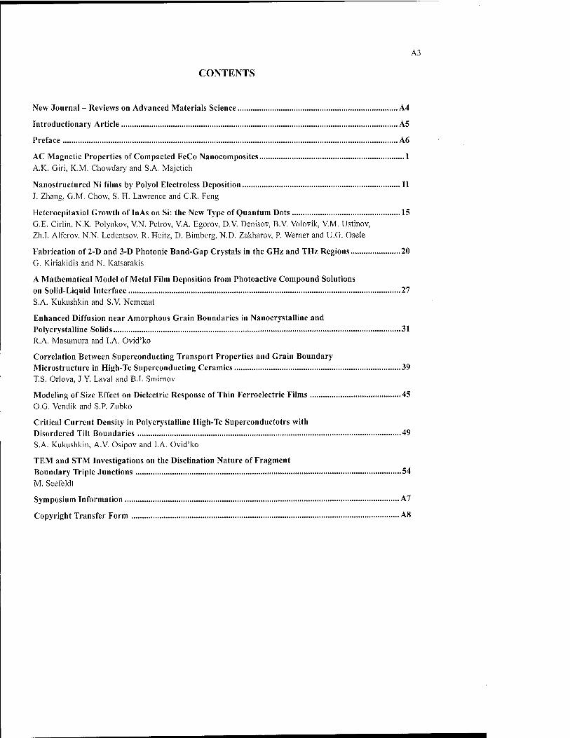
A3
CONTENTS
New Journal - Reviews on Advanced Materials Science A4
Introductionary Article A5
Preface A6
AC Magnetic Properties of Compacted FeCo Nanocomposites 1 A.K. Giri, K.M. Chowdary and S.A. Majetich
Nanostructured Ni films by Polyol Electroless Deposition 11 J. Zhang, G.M. Chow, S. H. Lawrence and C.R. Feng
Heteroepitaxial Growth of InAs on Si: the New Type of Quantum Dots 15 G.E. Cirlin, N.K. Polyakov, V.N. Petrov, V.A. Egorov, D.V. Denisov, B.V. Volovik, V.M. Ustinov, Zh.I. Alferov, N.N. Ledentsov, R. Heitz, D. Bimberg, N.D. Zakharov, P. Werner and U.G. Osele
Fabrication of 2-D and 3-D Photonic Band-Gap Crystals in the GHz and THz Regions 20 G. Kiriakidis and N. Katsarakis
A Mathematical Model of Metal Film Deposition from Photoactive Compound Solutions on Solid-Liquid Interface 27 S.A. Kukushkin and S.V. Nemenat
Enhanced Diffusion near Amorphous Grain Boundaries in Nanocrystalline and Polycrystalline Solids 31 R.A. Masumura and I.A. Ovid'ko
Correlation Between Superconducting Transport Properties and Grain Boundary Microstructure in High-Tc Superconducting Ceramics 39 T.S. Orlova, J.Y. Laval and B.I. Smirnov
Modeling of Size Effect on Dielectric Response of Thin Ferroelectric Films 45 O.G. Vendik and S.P. Zubko
Critical Current Density in Polycrystalline High-Tc Superconductotrs with Disordered Tilt Boundaries 49 S.A. Kukushkin, A.V. Osipov and I.A. Ovid'ko
TEM and STM Investigations on the Disclination Nature of Fragment Boundary Triple Junctions 54 M. Seefeldt
Symposium Information A7
Copyright Transfer Form A8
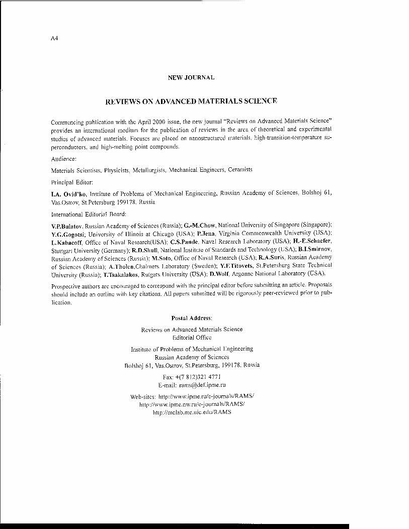
A4
NEW JOURNAL
REVIEWS ON ADVANCED MATERIALS SCIENCE
Commencing publication with the April 2000 issue, the new journal "Reviews on Advanced Materials Science" provides an international medium for the publication of reviews in the area of theoretical and experimental studies of advanced materials. Focuses are placed on nanostructured materials, high-transition-temperature su-
perconductors, and high-melting point compounds.
Audience:
Materials Scientists, Physicists, Metallurgists, Mechanical Engineers, Ceramists
Principal Editor:
I.A. Ovid'ko, Institute of Problems of Mechanical Engineering, Russian Academy of Sciences, Bolshoj 61,
Vas.Ostrov, St.Petersburg 199178, Russia
International Editorial Board:
V.P.Bulatov, Russian Academy of Sciences (Russia); G.-M.Chow, National university of Singapore (Singapore); Y.G.Gogotsi; University of Illinois at Chicago (USA); P.Jena, Virginia Commonwealth University (USA); L.Kabacoff, Office of Naval Research(USA); C.S.Pande, Naval Research Laboratory (USA); H.-E.Schaefer, Stuttgart University (Germany); R.D.ShuIl, National Institute of Standards and Technology (USA); B.I.Smirnov, Russian Academy of Sciences (Russia); M.Soto, Office of Naval Research (USA); R.A.Suris, Russian Academy of Sciences (Russia); A.Tholen,Chalmers Laboratory (Sweden); Y.F.Titovets, St.Petersburg State Technical University (Russia); T.Tsakalakos, Rutgers University (USA); D.Wolf, Argonne National Laboratory (USA).
Prospective authors are encouraged to correspond with the principal editor before submitting an article. Proposals should include an outline with key citations. All papers submitted will be rigorously peer-reviewed prior to pub-
lication.
Postal Address:
Reviews on Advanced Materials Science Editorial Office
Institute of Problems of Mechanical Engineering Russian Academy of Sciences
Bolshoj 61, Vas.Ostrov, St.Petersburg, 199178, Russia
Fax:+(7 812)321 4771 E-mail: [email protected]
Web-sites: http://www.ipme.ru/e-journals/RAMS/ http://www.ipme.nw.ru/e-journals/RAMS/
http://mclab.me.uic.edu/RAMS
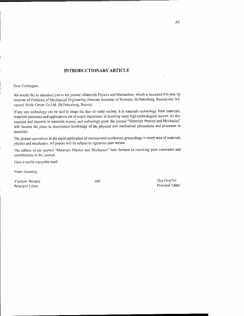
A5
INTRODUCTIONARY ARTICLE
Dear Colleagues,
We would like to introduce you to the journal «Materials Physics and Mechanics», which is launched this year by Institute of Problems of Mechanical Engineering (Russian Academy of Sciences, St.Petersburg, Russia) and Ad-
vanced Study Center Co.Ltd. (St.Petersburg, Russia).
If any one technology can be said to shape the face of today society, it is materials technology. New materials, materials processes and applications are of major importance in boosting many high technological sectors. As dis- cussions and intererst in materials science and technology grow, the journal "Materials Physics and Mechanics" will became the place to disseminate knowledge of the physical and mechanical phenomena and processes in
materials.
The journal specializes in the rapid publication of international conference proceedings in every area of materials
physics and mechanics. All papers will be subject to rigourous peer review.
The editors of the journal "Materials Physics and Mechanics" look forward to receiving your comments and
contributions to the journal.
Have a useful enjoyable read!
Yours sincerely,
Vladimir Bulatov and Ilya Ovid'ko Principal Editor Principal Editor
A6
PREFACE
This volume is a collection of selected original papers presented at the International Workshop on Applied As- pects of Interfaces Science (St.Petersburg, Russia, September 22-24, 1999). The workshop successfully provided a critical, up-to-date tutorial review and discussion on applied science of nanostructured materials and polycrystal- line high-Tc superconductors. Focuses were placed on synthesis, proccessing, characterization, properties, and applications of nanostructured materials and polycrystalline superconductors. A total of 33 scientists from 8 countries (Belgium, France, Germany, Russia, Singapore, South Africa, UK, USA) participated in the workshop,
making it a really international event.
About equal number of papers in this volume cover theoretical and experimental research in the area of interface science. All papers have been peer-reviewed prior to publication.
Support of the workshop from the Office of the US Naval Research, International Field Office, Europe; the European Office of the US Aerospace Research and Development, UK; and the European Research Office of the US Army, UK is greatly appreciated. Administrative support of the Institute of Problems of Mechanical Engineering (Russian Academy of Sciences, St.Petersburg, Russia) is also acknowledged.
IlyaOvid'ko Chairman, Organizing Committee
Mater.Phys.Mech.l (2000) 1-10
AC MAGNETIC PROPERTIES OF COMPACTED FeCo NANOCOMPOSITES
Anit K. Giri, Krishna M. Chowdary and Sara A. Majetich
Department of Physics. Carnegie Mellon University Pittsburgh, PA 15213^-3890. USA
Received: September 23, 1999
Abstract. Here we report the AC magnetic properties of soft magnetic nanocomposites made from compaction of Fe Co91) nanoparticles. Following a discussion of previous work on soft magnetic nanocomposites, the sample preparation and experimental characterization by AC permeametry are described. The permeability is constant and equal to the DC value for low frequencies, but drops off sharply above a characteristic frequency f. A model is developed to explore the relation between f and material parameters including the effective anisotropy, exchange coupled volume, temperature, and saturation magnetization.
1. INTRODUCTION
Many recent developments in soft magnets, which are used in power applications, have been based on amorphous and nanocrystalline materials [1-5]. In amorphous solids the magnetocrystalline anisotropy K is by definition equal to zero, eliminating the main material-dependent contribution to the coercivity. The effective anisotropy K can also be low in nanocrystalline materials if conditions specified by the Random Anisotropy Model are met [1-3, 6]. The grain size must be smaller than the magnetic exchange length L , and the grains must be exchange coupled with their easy axes for magnetization randomly oriented. The combination of random orientation and averaging over multiple grains makes the preference for magnetiza- tion in a particular direction, and therefore K p very small. Theoretically, low K materials become even softer if the grain size D is small enough. The DC magnetic properties of nanocomposites have been mod- eled in terms of the Random Anisotropy Model [1-3]. The magnetization reversal field or coercivity // is predicted to be proportional to D'\ while the perme- ability \x=B/H is predicted to be proportional to D'\ Here we extend this approach to understand the AC magnetic properties of nanocomposites.
Previous work on the AC magnetic properties of bulk magnetic materials has shown that the perme- ability can be split into in-phase (u.') and out-of-phase
(u") components, just like the permittivity of dielec- tric materials:
// = // -/// (1)
These components obey a Kramers-Krönig relationship [7], so that by knowing the value of one for all frequencies, the other is uniquely determined. The real part u' is typically flat up to a cutoff frequency, and then drops off, while the imaginary part u" shows a peak at the same frequency. In the best high frequency ferrite materials, the cutoff frequency is in the GHz range, and is associated with the precession frequency of spins about the applied magnetic field. While high frequency magnetic materials are highly insulating to reduce eddy current losses, their properties have not been analyzed in terms of their microstructure.
A benchmark for soft magnetic materials is the to- tal power loss, P , as the material is magnetized and demagnetized. It depends on the hysteresis loss, losses due to the eddy currents created by the changing mag- netic field, and anomalous losses associated with do- main wall motion [8], These contributions have differ- ent frequency dependencies:
p = p +p + p = Ui! hv.s t'fhly c urrcni onont
Wf + Af2/p+PmJf)- (2)
Ph varies linearly with the frequency/and the area within the hysteresis curve W. , P ,. is quadratic
J hys ctlclv current l
Corresponding author: Sara A. Majetich, e-mail: [email protected]
© 2000 Advanced Study Center Co. Ltd.

Anil K. Giri el al
in frequency and inversely proportional to the resistivity p. A is a constant. The anomalous loss P has no fixed power law dependence on the frequency.
The AC magnetic properties of ferrofluids, which are small (< 10 nm) magnetic particles dispersed in a liquid, show distinctly different behavior from that of bulk materials. There are two characteristic relaxation
times, one due to Brownian relaxation caused by rotation of the particles in the liquid, and the other due to Neel relaxation caused by coherent rotation of the atomic spins within the particle [9, 10]. Both processes occur at frequencies well below the Larmor frequency
fo- Nanocomposites have potential for two niche ap-
plications of soft magnetic materials. In low frequency applications, amorphous materials should continue to dominate, since they have the smallest hysteretic losses.
Without significant eddy currents, only the small per-
centage of atoms required for glass forming do not
contribute to the magnetization. However, at higher
temperatures amorphous materials crystallize. In the current nanocrystalline materials [1-5], grain growth is limited by precipitation of additional phases, and a larger fraction of nonmagnetic atoms is needed. At higher frequencies, nanocomposites have potential advantages because they can have higher resistivity to reduce eddy current losses. While ferrites are currently used for high frequency applications because of their high resistivities, they have much lower magnetiza- tions than iron-based alloys.
Iron-cobalt alloys are of interest for high tempera- ture soft magnets because they have a high Curie tem- perature, high magnetization, and low coercivity. The value of the Curie temperature depends on the relative Co abundance. Iron-cobalt alloys have the largest mag- netic moment per atom, and therefore large saturation magnetizations [11]. They have a low coercivity due to the low magnetocrystalline anisotropy K of the body- centered cubic structure. There is a zero crossing of the anisotropy near the equiatomic composition [12].
We investigate nanolaminates formed by compaction of FeCo nanoparticles with a very thin coating of a protective carbon or oxide. By choosing a particle or grain diameter well below the maximum monodomain size, the coercivity and hysteretic power losses can be minimized [1-3]. The coatings act as a barrier to eddy currents, reducing the eddy current power losses at high frequency. The goals are to minimize the portion of nonmagnetic atoms while retaining a stable nanocrystalline structure at high tem- perature, and to determine the degree of coating which retains significant exchange coupling for minimum K while creating significant barriers to eddy currents.
2. EXPERIMENTAL
Particle Synthesis. Here the alloy nanoparticles were synthesized by the polyol method [ 13], a chemical route which leads to highly monodisperse metal particles. Iron chloride tetrahydrate and sodium hydroxide were dissolved in ethylene glycol and heated to 110 °C while stirring. A second solution of cobalt hydroxide in eth- ylene glycol at the same temperature was added, and
the mixture was heated to 195 °C, where a precipitate formed. The total metal ion concentration was 0.2 M, and the hydroxide concentration was 2.0 M. Water and other reaction products were distilled off, and the sol- vent was re fluxed for one hour at the maximum tem- perature. The precipitate was thoroughly washed with methanol, and dried.
While the particle size can be varied by changing
the metal salt concentration and reaction time, the av-
erage grain diameter was roughly constant and approxi-
mately 20 nm. The composition was determined from
electron energy loss spectroscopy [14]. The average
grain size was obtained from Scherrer analysis of the x-ray diffraction peaks, and the particle size was found from transmission electron microscopy. The exchange length in magnetically soft materials like FeCo is large, and here is comparable to the grain size. Adjacent grains can then be exchange coupled to each other, leading to a further reduction in the anisotropy and coercivity, as explained by the random anisotropy model [1-3, 6]. Compaction. A nanocomposite has nanoparticle-sized grains, which may be dispersed in a matrix that medi- ates their coupling. The coupling strength depends on the magnetic behavior of the matrix and on the degree of coherence at the interface between the nanoparticles and the matrix. Exchange interactions may couple nanoparticles together. We worked with Dr. S. Sudarshan and Mr. Sang Yoo of Materials Modifica- tion, Inc., on plasma pressure compaction, which has the advantage of being able to reduce or remove the thin coating surrounding FeCo nanoparticles under ambient conditions. Powders were compacted by a combination of pressure and an electric arc in a two stage process. First a voltage pulse established a continuous current path across the sample in a graph- ite mold under a pressure of 10 MPa. This generated a plasma in the voids, and partly removed surface impurities such as oxides. In the second stage a continuous current path led to resistive sintering. The pressure was increased to 70 MPa to deform and compact the particles. The entire process required only a few minutes, thereby limiting grain growth. The resistive heating concentrated in the "necks" forming as the particles sinter, making them deform more

AC Magnetic Properlies of Compacted FeCo Nanocomposiles
20
W-
-100 -10
-20 25 0 25 50
H{VfOe)
-200 -100 100 200
A/(Oe)
Fig. 1. a.) Comparison of Fe Co nanoparticles made by the polyol method (open circles), and a compact made from them
(filled circles); b.) An expanded region shows the coercivity of the pellet is on the order of 5 Oe, much less than that of the
precursor particles, which is approximately 150 Oc.
readily. Compacts with over 90% theoretical density were made from the nanoparticle powders. Magnetic Properties. There was a substantial amount of magnetic characterization, including SQUID magne- tometry (with a Quantum Design MPMS) to determine the coercivity, and AC permeametry (with a Walker Sci- entific AC Hysteresisgraph) on toroidal compacts to measure the frequency dependence of the permeability m and the power loss. For the AC measurements, the toroid outer diameter was 2.54 cm, and it had a square cross section with dimensions 3.0x4.1 mm. There were 154 primary turns and 11 turns in the pickup coil. The amplitude of the AC magnetic field applied was 125 Oe, and the frequency ranged from 100 to 100,000 Hz. The temperature of the toroid was controlled by placing it in thermal contact with an ice bath (0°C), or with it inserted in a furnace (100 °C - 500 °C). At elevated tempera- tures the coils were sheathed with fiberglass sleeving (Omega Engineering, Inc.).
3. EXPERIMENTAL RESULTS
Fig. 1 shows a comparison of the DC hysteresis loops for the powder and compacted pellet of a typical sample. Compaction significantly reduces the coercivity, indi- cating that the exchange coupling is increased, as pre- dicted by the random anisotropy model.
The AC hysteresis loops were measured for toroids cut from the same compressed pellets, for a range of frequencies. With AC excitation, the pickup loop measures the magnetic induction B=-- 4nM-\-H. Fig. 2 illustrates the characteristic behavior as a function of frequency. At low frequencies (Fig. 2a) the applied field H was sufficient to saturate the sample, reaching the single-valued region of B{H). As the frequency was raised, the width of the hysteresis loop and therefore the coercivity increased, but the maximum induction remained approximately the same, up to a characteristic
frequency (Fig. 2b). Approaching this frequency, the sample was no longer saturated at the maximum ap- plied field, and the maximum magnetic induction dropped (Fig. 2c).
The permeability as a function of the maximum applied field is illustrated in Fig. 3, for several representative frequencies. Defining the permeability as the maximum value of B/H, it is expected to vary depending on the magnitude of Hmax. If Hma is small and the sample is not saturated, B increases approxi- mately linearly with H, and \x is large. If Hmax\s large and the sample is never saturated, B increases more slowly with increasing H and u is reduced. In order to understand the fundamental physics of the AC excita- tion of the nanocomposites, a value of Hmax = 125 Oe was selected for further measurements so that the samples were saturated at low frequency.
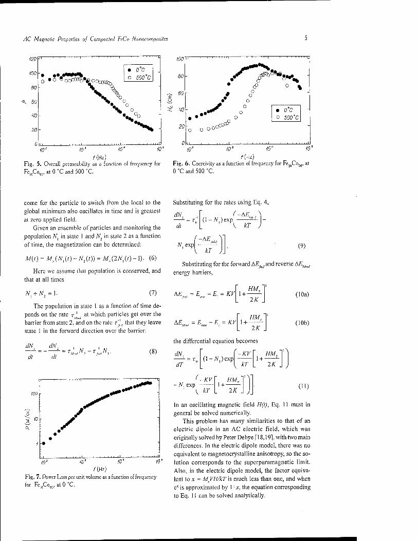
Several important quantities for soft magnetic ma- terials were measured as a function of frequency. The real (in-phase) and imaginary (out-of-phase) parts of the permeability \\.-B/H were also measured as a func- tion of frequency (Fig. 4). In the low frequency range, the phase lag between B and H is small, and u" is neg- ligible, u' is roughly constant up to the characteristic frequency, where it drops off sharply, u" peaks as u' drops off, and the critical frequency fc is determined from the position of the peak in u". The characteristic frequency of the permeability varied with temperature (Fig. 5). While the low frequency magnitude of m dropped off slightly with increasing temperature, due to a reduction in the magnetization, fc rose substan- tially, from 1400 Hz at 0 °C to 6000 Hz at 500 °C. As noted in the hysteresis loops, the coercivity rose with increasing frequency (Fig. 6). It peaked at a frequency approximately 2-3 times fc, and decreased somewhat at high frequencies. The overall power loss per cycle is shown in Fig. 7. At low frequencies it rises linearly, as expected from Eq. 2 if hysteretic losses are dominant.

03
10
5-
-10
-120
Anil K. Ciri el al
I ' I ' I ' ' l -L^vJasSi
c\- a / ̂ 7
«^"MSBftHP™ , JEMX»»»"— | i , i , i
-HO 0
H(Oe)
HO 80 120
Fig. 2. AC Hysteresis loops for Fe...Co(..., at 0 °C. a.) 100 Hz, b.) 800 Hz, c.) 5000 Hz.
At frequencies above/ a weaker dependence is ob- served, closer to/"5. As the temperature is increased
the power loss per cycle decreases somewhat, due
mainly to the reduction in the coercivity.
4. MODEL OF AC MAGNETIC PROPERTIES
Our model of the AC properties of nanocomposites is based on a monodomain magnetic particle in an oscillating magnetic field. For a uniaxial particle with the applied field parallel to the easy axis, the energy E is given by
E = KVsin2 6- Mßcosß, (3)
where K is the magnetocrystalline anisotropy, V is the particle volume, 8 is the angle between the magneti- zation direction and the applied field H, and M is the saturation magnetization. Stoner-Wohlfarth theory [15- 17] has shown that energy minima occur at 8 = 0° or 180°, and a maximum exists where cos8 =-HM/2K.
a,
I I I
" oc6)o0on
1 1 1
- dUU f = 500 Hz f = 900 Hz
250 °o
.^..°° 0 -4— AA -° ft
f =1MO0 Hz
- 200
150
100 f A
A •o A 8
50 -
n 1 1 1 i i i _ 20 HO 60 80 100 120
Fig. 3. Overall permeability for Fc.()Co(J()! as a function of Hmay, at 0 "C, for 500, 900, and 1400 Hz. The peak permeability at 22 Oc reflects where the slope of the B(H)
starts to decrease.
In order to reverse the magnetization direction, the
energy barrier must be overcome. If this does not oc-
cur within the measurement time, then hysteresis is
observed. The rate of going over the barrier r~' is given
by
r = r„ exp| A£
kT (4)
where r~ =f is the Larmor frequency, AE is the mag- nitude of the energy barrier, k is the Boltzmann constant, and T is the temperature.
If the magnetic field oscillates in time,
H(l) = H„ cos(2;z■//), (5)
then the positions of the energy minima and maxima will also change with time, as shown in Fig. 8. Early in the cycle state 1 is the global minimum and state 2 is a local minimum, but later the roles are reversed. The height of the energy barrier which must be over-
100
80
^ 60 X
HO
20
11
-• • •* _%
1 1 1. • 1 1 1 1 11
o ß"
-
<$ /^ N -
-o o
o o°° V.
-
-1 1 , r
10' 10' 10" 10'
KHz)
Fig. 4. The real (u.') and imaginary (|i") parts of the permeability for Fe Co , at 0 °C, as a function of frequency.
AC Magnetic Properties of Compacted FeCo Nanocomposites
120 ji
o
11
• o 8
1 ' ' ' "1 ' '—' i i i irj -"1
100 nrCP$h*£> nn
• o°c o 500°C
-
80
a, 60
W
20
0 1 1 1 1 1 1 I.I i i 1 1—1—1—1-
-
10' 10' 10"
/'(Hz)
100 J! 1 1 1 1 111
J**--%*
1 1 1 1 1 llL
80 • • ° %
'Tn 60 o o CJ
10
• • •••'
o
:£ o o •
o o°c 500° C '
20 o o o -
rt -, i 1 1 r
10*
Fig. 5. Overall permeability as a function of frequency for
Fe10Co%, at 0 °C and 500 °C.
10' iO" 10" ■10°
/(Hz) Fig. 6. Coercivity as a function of frequency for Fe|0Co0|), at
0 °C and 500 "C.
come for the particle to switch from the local to the global minimum also oscillates in time and is greatest at zero applied field.
Given an ensemble of particles and monitoring the population N in state 1 and N2 in state 2 as a function of time, the magnetization can be determined:
M{t) = Ms(Nl(t)-Ni(t)) = Ms(2Ni{t)-\). (6)
Here we assume that population is conserved, and that at all times
N.+N, =1. (7)
/.,-,/ state 1 in the forward direction over the barrier:
dNl
dt
dN1
dt = T N - T N
Mir,; 2 fn-ii i ■ (8)
Fig. 7. Power Loss per unit volume as a function of frequency
for Fe)0Co%, at 0 °C.
Substituting for the rates using Eq. 4,
dNt
dt
- N exp
(1-AMexpl
kT
bfo
kT
(9)
Substituting for the forward AE, , and reverse AE,, .
energy barriers,
AE = E -E=KV fml max 1
The population in state 1 as a function of time de- pends on the rate T~' at which particles get over the barrier from state 2, and on the rate T~' that they leave AE
1 + - 2K
E -E=KV 1+- HMS
2K
(10a)
(10b)
the differential equation becomes
I -AC = r„ (l-A/,)exp 1 + -
dN,
dT kT 2K
N exp -KV
kT IK
i\
(11)
In an oscillating magnetic field H(t), Eq. 11 must in general be solved numerically.
This problem has many similarities to that of an electric dipole in an AC electric field, which was originally solved by Peter Debye [18,19], with two main differences. In the electric dipole model, there was no equivalent to magnetocrystalline anisotropy, so the so- lution corresponds to the superparamagnetic limit. Also, in the electric dipole model, the factor equiva- lent to x = M VH/kT is much less than one, and when ex is approximated by 1 +x, the equation corresponding to Eq. 11 can be solved analytically.

Anil K. Cm el al
Time
Fig. 8. Energy levels as a function of time, for different parts of the cycle of H(l). Here E is the energy of a particle in state 1, E2 is the energy of a particle in state 2, and A£ is the magnitude of the barrier between the local minimum and the maximum energy states.
Equation 11 can be solved analytically in the limit
of large K, where &Efwd K ^Ebkwd- With the substitu- tion
KV
Eq. 11 then simplifies to
-^*r„V(l-2/V,). at
The solution to Eq. 13 is given by
tfl(0 = -[l + exp(-2r>)]-
(12)
(13)
(14)
There will be a characteristic or resonant frequency /', where
/: = r„e rT~:\ (-KV
exp 7i V kT
(15)
where the population oscillates in resonance with the driving field H(1). Above this frequency, the popula- tion shifts cannot keep up with the rapidly changing driving field.
The model breaks down for cases where HMJ2K> l, since this requires that \cos9=-HMJ2K\ be greater than one. To investigate the small K limit, which is of critical importance for soft magnetic materials, we reduced the amplitude of the magnetic field H where necessary. In experiments it is possible to have large amplitudes of the AC magnetic field when studying materials with very low anisotropy. Here the sample is being driven past the high slope portion of the hyster-
esis curve during each half-cycle. In applications of soft magnetic materials, this is undesirable since the permeability p =B/H is reduced. Therefore the model can be used to understand the AC magnetic behavior in situations of greatest technological importance.
5. MODELING RESULTS AND COMPARISON WITH EXPERIMENT
The simulation results show the same characteristics as the experimental data, and provide insight about the mechanism responsible for the frequency depen- dent behavior.
Fig. 9 illustrates the connection between the time- dependence of AY and the B(H) curves for driving fields of different frequencies// ~-H cos(2nft). If the frequency is low enough (Fig. 9a) the sample has time to equili- brate with the slowly varying field and superparamagnetism is observed. There is a negligible phase lag 9 between M(t) and H(t). Because of this M(t) reaches its maximum value well below the maximum amplitude of the driving field Hn. At somewhat higher frequencies M(t) starts to lag behind H(l) significantly, leading to hysteresis (Fig. 9b). However M(t) still reaches its maximum value before H(l) starts to de- crease. At the critical frequency f this is no longer true (Fig. 9c), and the shape of Mfi) and the hysteresis loop change noticeably. B(H) no longer contains single valued regions, and the maximum value of B starts to decrease relative to its value at lower frequencies. At the highest frequencies M(t) and H(t) are almost completely out of phase and the maximum values of M(l) and B(H) are very small (Fig. 9d). The model simu- lates characteristics of the experimental results shown in Fig. 2, and shows that the shape and magnitude of

AC Magnetic Properties of Compacted FeCo Nanocomposites
f-fn-M'6
ß( Gauss)
40000
5000
-mo -50
superparamagnetic
50 400 /V(Oe)
-5000
-40000 /
-wo -50
-5000
-40000
.Hysteresis when M(t) lots U(t)
400
40000 ] 5000 . Bmax drops I
£ increases /
-400 -50 50 400
-5000 1 -40000 J
40000
5000
400 -50 50 jooy -5000
-40000
Fig. 9. M(l) and H(t), and the corresponding B(H) curves for a sphere of exchange coupled volume V an6 effective anisotropy K. a.) for a superparamagnetic particle, b.) for a monodomain but not superparamagnetic particle at low frequency/, c.) at med. /, and d.) at high /. Note that in a.) and b.) B(H) appears to saturate, but this is because 4ft M is so much larger than H. These simulations used the following parameters: Ms = 1000 emu/cc, H0 = 125 Oe, K = 1.95-105 erg/cc, T=273 K, and V =
1.47-10"18 cc. The critical frequency / was 1400 Hz.
B(H) depend on whether the magnetization of the ex- change coupled volume within the sample can equili- brate with the changing external magnetic field.
Figure 10 shows the corresponding trend in the permeability u as a function of frequency. At low fre- quencies it is constant and equal to the DC value, but as soon as M(t) is unable to reach its maximum value, B . and therefore m begin to drop, approaching zero
in the high frequency limit. This is in contrast to the experimental results shown in Fig. 5, where u decays more slowly. Such a difference would arise if the sample contained a distribution of characteristic frequencies f, perhaps related to a distribution of grain sizes.
Fig. 11 reveals the behavior of the simulated coercivity as a function of frequency. At low frequen- cies it follows Sharrock's Law [20]:
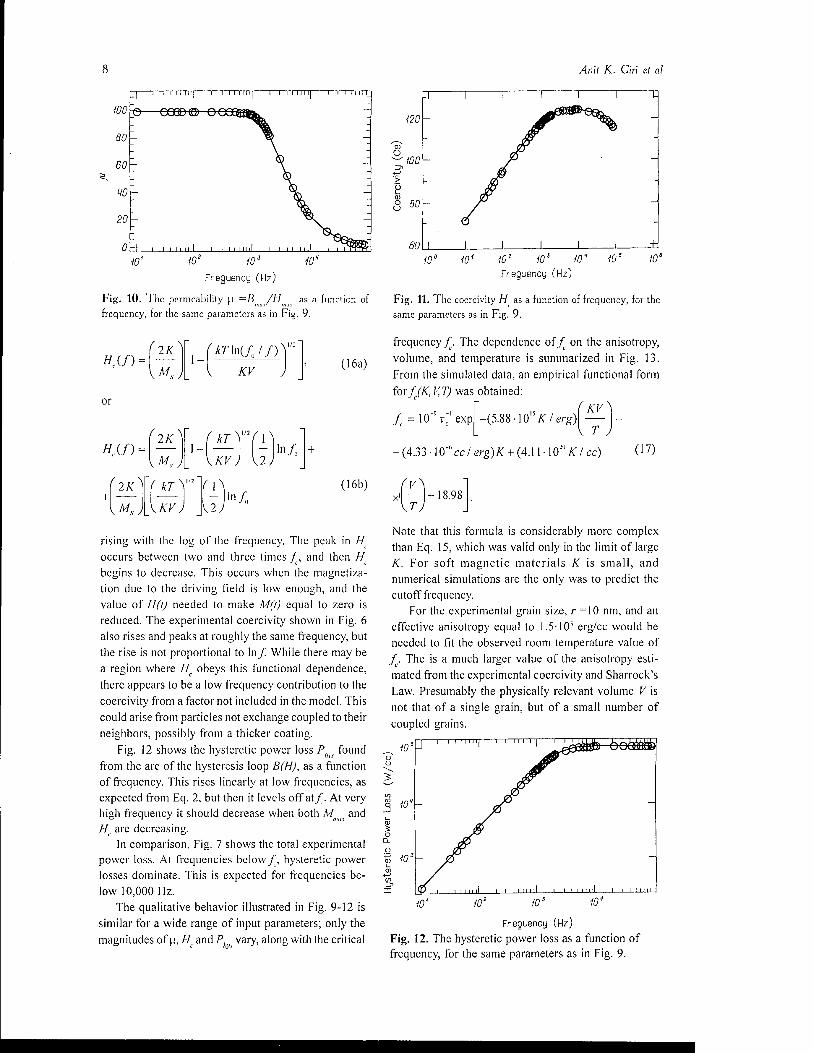
100
—1—I I 11 Mil
13 OOGDffi) Q(
^ 60 h
%
20
0\±. _J I
10< 10' 10'
Freguenoy (Hz)
10" 10 10"
Fig. 10. The permeability (.1 —B /H as a function of frequency, for the same parameters as in Fig. 9.
" (/) = '2K^
or
#(/) =
^
\MxJ
^2K^
\MsJ
kT
KV
1-
kTHfJf) KV
kT
KV
(16a)
2|h/'
In/, (16b)
rising with the log of the frequency. The peak in H occurs between two and three times /,, and then H begins to decrease. This occurs when the magnetiza- tion due to the driving field is low enough, and the value of H(l) needed to make M(l) equal to zero is reduced. The experimental coercivity shown in Fig. 6 also rises and peaks at roughly the same frequency, but the rise is not proportional to In/.' While there may be a region where H obeys this functional dependence, there appears to be a low frequency contribution to the coercivity from a factor not included in the model. This could arise from particles not exchange coupled to their neighbors, possibly from a thicker coating.
Fig. 12 shows the hysteretic power loss Plis found from the are of the hysteresis loop B(H), as a function of frequency. This rises linearly at low frequencies, as expected from Eq. 2, but then it levels off at/. At very high frequency it should decrease when both M and Hc are decreasing.
In comparison, Fig. 7 shows the total experimental power loss. At frequencies below/, hysteretic power losses dominate. This is expected for frequencies be- low 10,000 Hz.
The qualitative behavior illustrated in Fig. 9-12 is similar for a wide range of input parameters; only the magnitudes of u, // and Ph i( vary, along with the critical
10' 10l 10" Freguency (Hz)
Fig. 11. The coercivity H as a function of frequency, for the same parameters as in Fig. 9.
frequency/. The dependence of/, on the anisotropy, volume, and temperature is summarized in Fig. 13. From the simulated data, an empirical functional form
forfc(K, V,T) was obtained:
/=10-Jr-'exp -(5.88-10l5A7erg)l —
- (4.33 -W*cclerg)K + (4.11 • 102" KI cc) (17)
x> (— |+18.98
Note that this formula is considerably more complex than Eq. 15, which was valid only in the limit of large K. For soft magnetic materials K is small, and numerical simulations are the only was to predict the cutoff frequency.
For the experimental grain size, r =10 nm, and an effective anisotropy equal to 1.5T05 erg/cc would be needed to fit the observed room temperature value of /,. The is a much larger value of the anisotropy esti- mated from the experimental coercivity and Sharrock's Law. Presumably the physically relevant volume V is not that of a single grain, but of a small number of coupled grains.
5 A ' l I Mlllj I 1 1 1 1 1 1 1] 1 I lUJiJJj, 10
10" -
10s - -
© i I I I mil I I I I mil 1 I i i. mil | 1 1 1 1 1 N
10' 102 103 10"
Freguenoy (Hz) Fig. 12. The hysteretic power loss as a function of frequency, for the same parameters as in Fig. 9.

AC Magnetic Properties of Compacted FeCo Nanocomposites
t &
10'
107
g° 10
^ 10'
150 200 250
Anisotropy (ergs/cc)
300-10'
T
/<= HO5 (ergs/cc)
KH.5'10s (ergs/cc)
/<=2--10s (ergs/cc)
J I— 1
T--271K
L_ 3 V 5
Volume (cc)
•■10'
(KV)c§H2-\V ergs
(KVfc W4-t0',1ergs
(KVk 2-88 10"" ergs __J I
2 3
I/Temperature (K'\
510
Fig. 13 a.) / as a function of the anisotropy for spheres of different radii. Here V=(47r/3)r>\ b.) / as a function of the volume; c.) / as a function of the inverse temperature.
6. CONCLUSIONS
The AC magnetic properties of soft magnetic nanocomposites made from compaction of Fe10Cogn
nanoparticles can be understood in terms of an effective anisotropy and a related exchange coupled volume. The permeability is constant and equal to the DC value for low frequencies, but drops off above a characteristic frequency /\ For bulk materials such as ferrites the cutoff frequency can be extremely high, and the be- havior is understood in terms of the Landau-Lifshitz- Gilbert equation [21-23]. However for compacted nanocomposites the cutoff frequency is much lower,
and depends on the sample microstructure. The value of this frequency can be increased by raising the tem- perature, or by reducing the anisotropy and grain size. Experiments are in progress to prepare samples to fur- ther test this model.
ACKNOWLEDGMENTS
This work was supported in part by the National Sci- ence Foundation under Grant numbers DMR-9900550
and ECD-8907068, and by the Air Force Office of Sci- entific Research under grant number F49620-96-1- 0454. The assistance of K. Humfeld and N. Ide in the simulations is greatly appreciated.
REFERENCES
I] G. Herzer// IEEE Trans. Mag. 25 (1989) 3327. 2] G. Herzer // IEEE Trans. Mag. 26 (1990) 1397. 3] G. Herzer IIJ. Magn. Magn. Mater. 112 (1992)
258. 4] Y. Yoshizawa, S. Oguma and K. Yamauchi II J.
Appl.Phys. 64(1988)6044. 5] A. Makino, T. Hatani, Y. Naitoh, T. Bitoh, A.
Inoue and T. Masumoto // IEEE Trans. Mag. 33 (1997) 3793.
6] R. Alben, J. J. Becker and M. C. Chi //./. Appl.
Phys. 49 (1978) 1653. 7] N. Ashcroft and D. Mermin, Solid Slate Physics
(Harcourt Brace, NY, 1976). 8] R. A. McCurrie, Ferromagnetic Materials:
Structure and Properties (Academic Press, NY, 1994).
9] J. Zhang, C. Boyd and W. Luo // Phys. Rev. Lett. 77(1996)390.
10] M. I. Shliomis and V. I. Stepanov, in Advances in Chemical Physics, ed. W. Coffey (Wiley, NY, 1987)87 1.
II] C. W. Chen, Magnetism and Metallurgy of Soft Magnetic Materials (Dover, NY, 1986).
12] F. Pfeifer and C. Radeloff//./. Magn. Magn. Mat. 19(1980) 190.
13] G.Viau, F. Fievet-Vincent and F. Fievet IIJ. Mater. Chem. 6 (1996) 1047.
14] J. H. J. Scott, Z. Turgut, K. Chowdary, M. E. McHenry and S. A. Majetich II Mat. Res. Soc. Symp. Proc. 501 (1998) 121.
15] E. C. Stoner and E. P. Wohlfarth // Phil. Trans. Roy. Soc. A240( 1948) 599.
16] W. F. Brown, Jr. IIJ. Appl. Phys. 29 (1958) 470. 17] W. F. Brown, Jr. //./. Appl. Phys. 30 (1959) 130. 18] A. K. Jonscher, Dielectric Relaxation in Solids
(Chelsea Dielectrics Press, Ltd., London, 1983). [19] P. Debye, Polar Molecules (Chemical Catalog
Co., NY, 1929).

10
[20] M. P. Sharrock // IEEE Tram. Mag. 26 (1990) [22] T. L. Gilbert, Ph. D. thesis, Illinois Institute of 193. Technology, Chicago, IL, June 1956.
[21] L. Landau and E. Lifshitz // Phys. Z [23] H. B. Callen // J. Phys. Chem. Solids 4 (1958)
Sowjetunion 8 (1936) 153. 256.

Mater.Phys.Mech.l (2000)
NANOSTRUCTURED Ni FILMS BY POLYOL ELECTROLESS DEPOSITION
J. Zhang1, G.M. Chow1, S.H. Lawrence2 and C.R. Feng2
'Department of Materials Science, National University of Singapore, Kent Ridge, Singapore 117543, Republic of Singapore
2Naval Research Laboratory, Washington, DC 20375, USA
Received: November 17, 1999
Abstract. Nanostructured Ni films were deposited on Cu by reducing nickel acetate tetrahydrate in refluxing cthylene glycol at about 194 °C. The effects of deposition time (t) and Pt as nucleating aid were investigated in this polyol process. The solution chemistry varied with t. At longer /, corrosive attack of the solvent on deposited films led to dissolution and re-deposition of Ni. Saturation magnetization increased with ( and decreased with increasing Pt precursors. The deposited Ni films were magnetically saturated. They showed in-plane magnetization anisotropy and perpendicular coercivity anisotropy. The use of Pt caused rapid powder precipitation but did not enhance film deposition. The Pt-catalyzed Ni films showed a (200) texture and a higher squareness ratio.
1. INTRODUCTION
Nanostructured films have attracted much attention because of their unique properties that arise from ef- fects of size reduction and large amount of interfaces [1]. These films can be prepared by many methods, for example, sputtering, laser ablation, electrodeposition and electroless deposition. For uniform metallization of non-planar and/or hidden surfaces, solution chemistry is better suited than the physical vapor methods, since it is not limited by the line-of-sight depo- sition.
An electroless polyol method, which has been mainly used to synthesize micron, submicron and nanostructured powders [1-8], has been recently ap- plied for deposition of nanostructured metal films, for example, Cu film on A1N substrate [9] and NixCo100_x
film on Cu substrate [101. The Ni Co... films exhib- L J x 100-x
ited good magnetic properties with perpendicular coercivity anisotropy [10]. The structure of these films have been recently investigated using anomalous x- ray scattering to determine if a solid solution or phase- separated composite was formed and the element-se- lected long range order [11]. To date, the film deposi- tion chemistry and mechanisms of this polyol process are not yet well understood. Unlike physical vapor depo- sition where the flux of atoms can be maintained constant, the solution chemistry (thus deposition
chemistry) may vary as a function of deposition (reaction) time.
In this paper, we report our investigation of the magnetic properties of polyol-deposited Ni films and their dependence on the deposition time (/). The ef- fects of increasing t on crystallite size, film thickness, microstructures and magnetic properties were studied. The influence of Pt as nucleating aid, which has been used in polyol synthesis of powders [12], on Ni film deposition was also studied.
2. EXPERIMENTAL
Polycrystalline, coarse-grained copper with (200) tex- ture was used as substrates without any pre-deposition surface treatment or polishing. 0.1 M nickel acetate tetrahydrate was suspended in 200 ml ethylene glycol. Hexachloroplatinic acid in small quantity was added in reactions where the effects of nucleating aid were investigated. The ratio of concentration of Pt to Ni ([Pt]/[Ni]) was estimated from the starting precursors. The substrate was vertically suspended in the mixture, which was brought to reflux at about 194 °C. Deposi- tion time (/ = 0.5, 1, 2 and 3 h) was taken on the base of the time required to reach the the refluxing tem- perature. After each deposition, the coated sample was immediately removed from the mixture, rinsed with
Corresponding author: G.M. Chow, e-mail: [email protected]
© 2000 Advanced Study Center Co. Ltd.
12 /. Zhang et al
16
M
3 en 4 m o> c
B 0.8 *-> B 0.6
QM
0.2
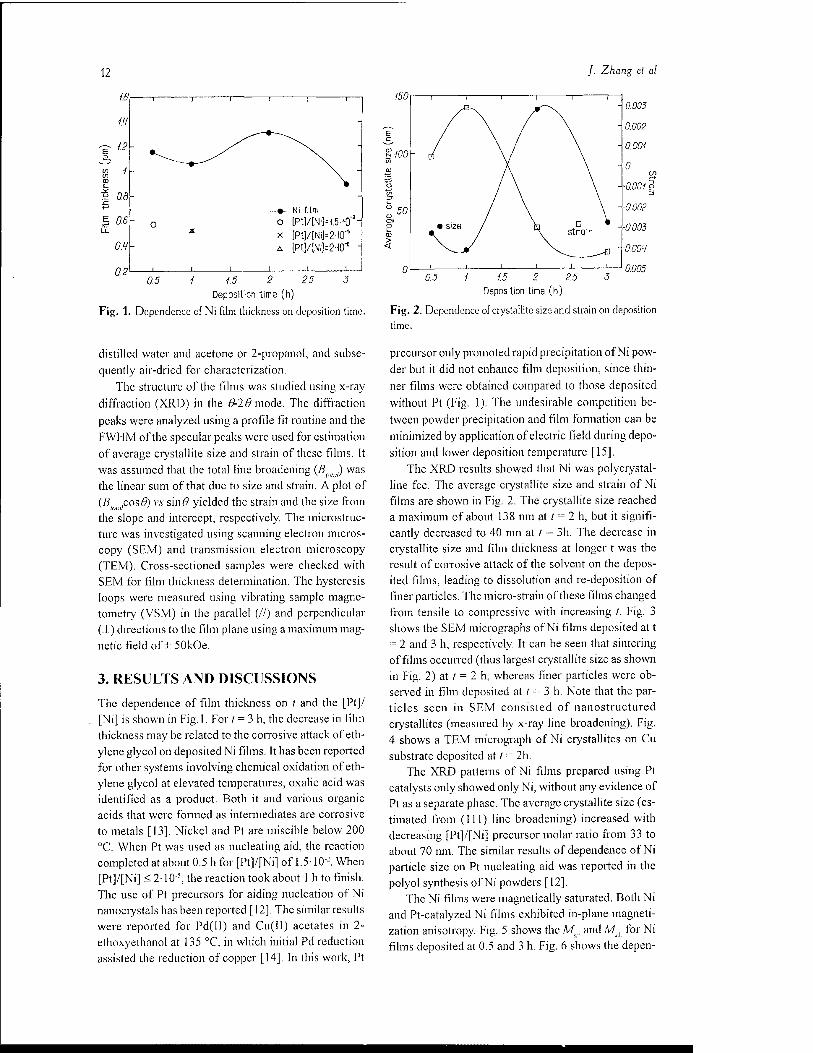
Fig. 1.
-•-Ni film O [Pt]/[Ni]=15-lO"a
x [Pt]/[Ni]=210'5
A [Pt]/[Nij-2-ffl"*
0.5 1 1.5 2 2.5 3 Deposition time (h)
Dependence of Ni film thickness on deposition time.
distilled water and acetone or 2-propanol, and subse- quently air-dried for characterization.
The structure of the films was studied using x-ray diffraction (XRD) in the #-20 mode. The diffraction
peaks were analyzed using a profile fit routine and the FWHM of the specular peaks were used for estimation of average crystallite size and strain of these films. It was assumed that the total line broadening (BloH) was the linear sum ofthat due to size and strain. A plot of (ßioi:lcosß) v.y sin# yielded the strain and the size from the slope and intercept, respectively. The microstruc- ture was investigated using scanning electron micros- copy (SEM) and transmission electron microscopy (TEM). Cross-sectioned samples were checked with SEM for film thickness determination. The hysteresis loops were measured using vibrating sample magne- tometry (VSM) in the parallel (//) and perpendicular (1) directions to the film plane using a maximum mag- netic field of ± 50kOe.
3. RESULTS AND DISCUSSIONS
The dependence of film thickness on / and the [Pt]/ [Ni] is shown in Fig. 1. For / = 3 h, the decrease in film thickness may be related to the corrosive attack of eth- ylene glycol on deposited Ni films. It has been reported for other systems involving chemical oxidation of efh- ylene glycol at elevated temperatures, oxalic acid was identified as a product. Both it and various organic acids that were formed as intermediates are corrosive to metals [13]. Nickel and Pt are miscible below 200 °C. When Pt was used as nucleating aid, the reaction completed at about 0.5 h for [Pt]/[Ni] of 1.5-10"2. When [Pt]/[Ni] < 2-105, the reaction took about 1 h to finish. The use of Pt precursors for aiding nucleation of Ni nanocrystals has been reported [12]. The similar results were reported for Pd(II) and Cu(II) acetates in 2- ethoxyethanol at 135 °C, in which initial Pd reduction assisted the reduction of copper [14]. In this work, Pt
150
Uoo
50
1 1 1 i i i
-
• size / ^. strain
i
0.5
0.003
0.002
0001
0
■0.001 D
-0.002
-0003
0.00'-/
0.005
Fig. time
1 15 2 2.5
Deposition time (h)
2. Dependence of crystallite size and strain on deposition
precursor only promoted rapid precipitation of Ni pow- der but it did not enhance film deposition, since thin-
ner films were obtained compared to those deposited
without Pt (Fig. 1). The undesirable competition be- tween powder precipitation and film formation can be minimized by application of electric field during depo- sition and lower deposition temperature [15].
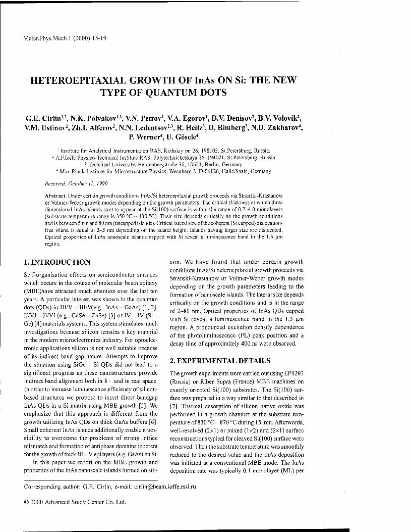
The XRD results showed that Ni was polycrystal- line fee. The average crystallite size and strain of Ni films are shown in Fig. 2. The crystallite size reached a maximum of about 138 nm at / = 2 h, but it signifi- cantly decreased to 40 nm at / = 3h. The decrease in crystallite size and film thickness at longer t was the result of corrosive attack of the solvent on the depos- ited films, leading to dissolution and re-deposition of finer particles. The micro-strain of these films changed from tensile to compressive with increasing /. Fig. 3 shows the SEM micrographs of Ni films deposited at t = 2 and 3 h, respectively. It can be seen that sintering of films occurred (thus largest crystallite size as shown in Fig. 2) at / = 2 h, whereas finer particles were ob- served in film deposited at / = 3 h. Note that the par- ticles seen in SEM consisted of nanostructured crystallites (measured by x-ray line broadening). Fig. 4 shows a TEM micrograph of Ni crystallites on Cu substrate deposited at / = 2h.
The XRD patterns of Ni films prepared using Pt catalysts only showed only Ni, without any evidence of Pt as a separate phase. The average crystallite size (es- timated from (111) line broadening) increased with decreasing [Pt]/[Ni] precursor molar ratio from 33 to about 70 nm. The similar results of dependence of Ni particle size on Pt nucleating aid was reported in the polyol synthesis of Ni powders [12],
The Ni films were magnetically saturated. Both Ni and Pt-catalyzed Ni films exhibited in-plane magneti- zation anisotropy. Fig. 5 shows the Ms., and MsL for Ni films deposited at 0.5 and 3 h. Fig. 6 shows the depen-

Nanoslructured N't Films by Polyol Ekclroless Deposition
a) in, ymm *>T*.
13
Fig. 3. SEM micrographs of Ni films deposited at : a) 2 h.
b) 3 h.
100 nm
Fig. 4. TEM bright field micrograph of Ni film on Cu
substrate deposited at 2 h. Dark particles arc Ni.
dence of A/.. //..., and //± of Ni films on /. The A/ of bulk fee Ni is about A/ is 484 emu/cm3. The values of M increased with / and reached 405 emu/cm3 for the Ni film deposited 3 h. This may be due to the increased film density at longer /. For films consisting of randomly oriented crystallites, the squareness ratio (ratio of remanent magnetization. A/, to saturation magnetization. A/) is typically about 0.5. This ratio was between 0.4 and 0.5 for Ni films, except it was higher forthat deposited at 1 h (about 0.6). Fig. 7 shows M and the squareness ratio of Ni films deposited with Pt catalysts. AT, increased whereas squareness ratio
500
-250
,-250
-500 -20 0 20
Magnetic field (kOe)
Fig. 5. Hysteresis loops of Ni films deposited at 0.5 h and 3
h, showing magnetic saturation and in-plane anisotropy.
500
^W
^300
9,200
100
0
-Ms II M Nc perpendicular -a- Hc II
300
250
-200
150
■ -a .-o - 100
50 0.5 1 15 2 2.5 3
Deposition time (h)
Fig. 6. Dependence of saturation magnetization and coercivity
of Ni films on deposition time.
decreased with decreasing [Pt]/[Ni]. The deposition time forNi films using [Pt]/[Ni] of2-10"5 and 2-10"6 was about 1 h, and was 0.5 h for [Pt]/[Ni] of 1.5-102. Pt had a predominant effect on Ms//and a lower [Pt]/[Ni] ratio led to a higher Ms as expected. Lower A/ may be related to alloying of Pt with Ni. Examination of XRD data of these films showed a (200) texture. This is consistent with the higher squareness ratio (between 0.56 to 0.65) of these films. Fig. 8 shows that the films deposited with Pt catalysts also had higher perpendicular coercivity. The coercivity anisotropy may be related to the microstructures of deposited film [15]. The work is currently underway to investigate the structure and microstructure of these films by transmission electron
microscopy.
4. SUMMARY
Nanostructured Ni films were deposited by the polyol method on Cu substrates with or without Pt as nucleat- ing aid. The solution chemistry varied with t. At longer

14 /. Zhang el al
15-10" 2.0-10'' 2.0- 10'" [Pt]/[Ni] percursor motor ratio
Fig. 7. Dependence of saturation magnetization and square ratio of Ni films on [Pt]/[Ni] precursor molar ratio.
WO
300
> 200-
1.5-10° 2.0-W> 2.0 -10's
[Pt]/[Ni] percursor motor ratio Fig. 8. Dependence of coercivity of Ni films on [Pt]/[Ni] precursor molar ratio.
/, coiTosive attack of the solvent on deposited films led to dissolution and re-deposition of Ni. Saturation mag-
netization increased with / and decreased with increas- ing Pt precursor concentration. The magnetically satu-
rated films showed in-plane magnetization anisotropy
and perpendicular coercivity anisotropy. The use of Pt favored rapid powder precipitation but did not enhance film deposition. The Pt-catalyzed Ni films showed a (200) texture and a higher squareness ratio. Further work is needed to understand the solution chemistry and film deposition chemistry in the polyol process.
ACKNOWLEDGMENTS
GMC thank the support of this work by the Academic Research Grant of the National University of Singapore and the US Office of Naval Research. J. Zhang was supported by the NUS postgraduate research scholar- ship.
REFERENCES
[1] G.M. Chow, I. Ovid'ko and T. Tsakalakos (eds.), Nanostruclured Films and Coalings, NATO Advanced Research Workshop, Santorini, Greece (Kluwer Publications, the Netherlands, 2000, in
press). [2] F. Fievet, J.P. Lagier and M. Figlarz // Mater.
Res. Soc. Bull. (1989)29. [3] F. Fievet, J.P. Lagier, B. Blin, B. Beaudoin and
M. Figlarz II Solid Stale Ionics 32/33 (1989) 198. [4] G. Viau, F. Ravel, O. Acher, F. Fievet -Vincent
and F. Fievet //./. Appl. Phys. 76 (1994) 6570.
[5] L.K. Kurihara, G.M. Chow and P.E. Schoen //
Nanoslnictur. Mater. 5 (1995) 607. [6] G.M. Chow, L.K. Kurihara, K.M. Kemner, P.E.
Schoen, W.T. Elam, A. Ervin, S. Keller, Y.D.
Zhang, J. Budnick and T. Ambrose //./. Mater.
Res. 10(1995) 1546. [7] G Viau, F. Fievet -Vincent, and F. Fievet // Solid
State Ionics 84 (1996)259. [8] G. Viau, F. Fievet-Vincent and F. Fievet //./. Mater.
Chem. 6(1996) 1047. [9] G.M. Chow, L. K. Kurihara, D. Ma, C. R. Feng,
P.E. Schoen and L.J. Martinez-Miranda // Appl. Phys. Lett. 70(1997)2315.
[10] G.M. Chow, J. Ding, J. Zhang, K.Y. Lee, D. Surani and S.H. Lawrence II Appl. Phys. Lett.
74(1999) 1889. [11] G.M. Chow, W.C. Goh, Y.K. Hwu, T.S. Cho,
J.H. Je, H.H. Lee, H.C. Kang, D.Y. Noh, C. K. Lin and W. D. Chang // Appl. Phys. Lett. 75 (1999)2503.
[12] M.S. Hedge, D. Larcher, L. Dupont, B. Beaudion, K. Tekaia-Elhsissen and J.-M. Tarascon // Solid Slate Ionics 93 (1997) 33.
[13] C.B. Jordan, Engine Coolant Testing, Second Symposium, (American Society for Testing of
Metals, 1986), p. 249. [14] J.S. Bradley, E.W. Hill, C. Klein, B. Chaudret,
and J. Duteil // Chemistry of Materials 5 (1993)
254. [15] G.M. Chow, J. Zhang, YY. Li, J. Ding and W.C.
Goh // Mal. Sei. Eng. A, in press.
Mater.Phys.Mech.l (2000) 15-19
HETEROEPITAXIAL GROWTH OF InAs ON Si: THE NEW TYPE OF QUANTUM DOTS
G.E. Cirhn12, N.K. Polyakov12, V.N. Petrov1, V.A. Egorov1, D.V. Denisov2, B.V. Volovik2, V.M. Ustinov2, Zh.I. Alferov2, N.N. Ledentsov2 3, R. Heitz3, D. Bimberg3, N.D. Zakharov4,
P. Werner4, U. Gösele4
1 Institute for Analytical Instrumentation RAS. Rizhskiy pr. 26, 198103, St.Petersburg, Russia,
2 A.F.Ioffe Physico-Technical Institute RAS, Polytechnicheskaya 26, 194021, St.Petersburg, Russia 3 Technical University, Hardenbergstraße 36, 10623, Berlin, Germany
4 Max-Plank-Institute for Microstructure Physics, Wecnberg 2, D-06120, Halle/Saale, Germany
Received: October 11, 1999
Abstract. Under certain growth conditions InAs/Si heteroepitaxial growth proceeds via Stranski-Krastanow or Volmer-Weber growth modes depending on the growth parameters. The critical thickness at which three dimensional InAs islands start to appear at the Si(100) surface is within the range of 0.7-4.0 monolayers (substrate temperature range is 350 °C - 430 °C). Their size depends critically on the growth conditions and is between 5 nm and 80 nm (uncapped islands). Critical lateral size of the coherent (Si capped) dislocation- free island is equal to 2-5 nm depending on the island height. Islands having larger size are dislocated. Optical properties of InAs nanoscale islands capped with Si reveal a luminescence band in the 1.3 |im region.
1. INTRODUCTION
Self-organisation effects on semiconductor surfaces which occure in the course of molecular beam epitaxy (MBE)have attracted much attention over the last ten years. A particular interest was shown in the quantum dots (QDs) in III/V - III/V(e.g., InAs - GaAs) [1, 2], II/VI - II/VI (e.g., CdSe - ZnSe) [3] or IV - IV (Si - Ge) [4] materials systems. This system stimulates much investigations because silicon remains a key material in the modern microelectronics industry. For optoelec- tronic applications silicon is not well suitable because of its indirect band gap nature. Attempts to improve the situation using SiGe - Si QDs did not lead to a significant progress as these nanostructures provide indirect band alignment both in k - and in real space. In order to increase luminescence efficiency of silicon- based structures we propose to insert direct bandgap InAs QDs in a Si matrix using MBE growth [5]. We emphasize that this approach is different from the growth utilizing InAs QDs on thick GaAs buffers [6]. Small coherent InAs islands additionally enable a pos- sibility to overcome the problems of strong lattice mismatch and formation of antiphase domains inherent for the growth of thick III - V epilayers (e.g. GaAs) on Si.
In this paper we report on the MBE growth and properties of the InAs nanoscale islands formed on sili-
con. We have found that under certain growth conditions InAs/Si heteroepitaxial growth proceeds via Stranski-Krastanow or Volmer-Weber growth modes depending on the growth parameters leading to the formation of nanoscale islands. The lateral size depends critically on the growth conditions and is in the range of 2-80 nm. Optical properties of InAs QDs capped with Si reveal a luminescence band in the 1.3 urn region. A pronounced excitation density dependence of the photoluminescence (PL) peak position and a decay time of approximitely 400 ns were observed.
2. EXPERIMENTAL DETAILS
The growth experiments were carried out using EP1203 (Russia) or Riber Supra (France) MBE machines on exactly oriented Si(100) substrates. The Si(100) sur- face was prepared in a way similar to that described in [7]. Thermal desorption of silicon native oxide was performed in a growth chamber at the substrate tem- perature of 830 °C - 870 °C during 15 min. Afterwords, well-resolved (2x1) or mixed (1x2) and (2x1) surface reconstructions typical for cleaved Si(100) surface were observed. Then the substrate temperature was smoothly reduced to the desired value and the InAs deposition was initiated at a conventional MBE mode. The InAs deposition rate was typically 0.1 monolayer (ML) per
Corresponding author: G.E. Cirlin, e-mail: [email protected]
© 2000 Advanced Study Center Co. Ltd.

16
_ JASq/Jln ■-- —.
t :^:C-; ^^^ 8
1 » i
350 mo wo Substrote Temperature , °C
Fig. 1. Critical thickness dependence on substrate temperature
and JA.4/JI,I fluxes ratio during InAs/Si growth.
second. When the deposition of the desired average thickness of InAs had been completed, the sample was immediately quenched to the room temperature and removed from the growth chamber in order to perform scanning tunnelling microscopy (STM) and scanning electron microscopy (SEM) studies. SEM measurements were performed using CamScan setup. Pieces for STM studies were covered with silicon vacuum oil immediately after exposure to the atmo- sphere, a procedure used before in our studies of InAs QDs on GaAs surfaces [8]. A calibration of the growth rate, III - V flux ratio, and monitoring of the surface morphology during growth was performed using reflection high energy electron diffraction (RHEED) system composed of a high sensitivity video camera, a video tape recorder and a computer, all interconnected via specially-designed interface [9]. Transmission elec- tron microscopy (TEM) images were obtained on the samples when InAs islands were covered with 30-50 nm of silicon using JEOL 4000EX microscope. The same structures were used for luminescence experi- ments. A 514.5 nm line of the Ar+ laser was used as an excitation source and a Ge photodiode as a detector. The excitation density was 5-100 W/cm2. The struc- tures for TEM and PL studies were grown in a follow- ing manner. Just after InAs deposition, a 10-20 nm Si cap layer was grown at the same substrate temperature T as for InAs deposition followed by a 10 min annealing procedure at 650 °C - 700 °C. Then 20-40 nm of Si was grown at the same temperature with optional
C.E. Cirlin et al.
consequent 10 min annealing at 700 °C - 800 °C in order to smooth the resulting surface.
3. RESULTS AND DISCUSSION
In Fig.l we summarise RHEED data of the dependen- cies of the substrate temperatures and As4/In fluxes ratio in the ranges 350 °C - 450 °C and 2-12, respectively,
on the critical thickness dcrli (mean thickness at which 3D nanoscale islands start to appear at the surface). The lowest limit of Tt was chosen for two reasons: first, determination of r at very low temperatures is difficult and second, because of poor quality of Si cap layer grown at too low temperatures. Poor quality of the Si cap layer may hinder the device applications. On the other hand, we have found that at temperatures higher then 450 °C no nanoislanding is observed on
the surface independently on the V/III flux ratio, total arsenic overpressure, etc. limiting the range for the
highest r as indicated in Fig.l. (At higher Ts only
mesoscopic dislocated clusters with lateral size of-400 nm appeared on the Si(100) surface [10]). Following the data presented in Fig.l one can conclude that de- pending on the growth conditions, 2D-3D transition can be tuned in the thickness range of 0.7-4.0 ML. On the other hand, we have observed two different growth modes for the InAs/Si heteroepitaxial growth. First, Volmer-Weber growth mechanism could be realised when InAs nanoscale islands are formed on the bare Si substrate (i.e. for dcr<\ ML). Typical RHEED pat- tern for this case is presented in Fig. 2,a. At higher Ts
(400 °C - 450 °C) we observed Stranski-Krastanow growth mechanism when dmi exceeded 1.0 ML and the formation of InAs nanoscale islands occurs on the top of the wetting layer. RHEED pattern for this par- ticular case is presented in Fig. 2,b. These results are in agreement with the 2D - 3D transition intervals ob-
served by other groups [11, 12]. Typical surface morphology extracted from the STM
images for these cases revealed high density arrays of nanoscale islands (with surface density of the order of ((1^6)xl0" cm"2) and the lateral sizes of 10-20 nm [13, 14]. These islands are basically pyramidal in shape with rectangular or triangular base.
We have found that the growth conditions (the amount of InAs deposited, fluxes ratio influenced greately the arrangement, sizes and surface density of InAs/Si islands [15]. In order to clarify how growth parameters influence the surface morphology we grew three samples, labelled 1-3. Their MBE growth conditions and geometrical characteristics measured with SEM are presented in the Table 1.
The main trends for the uncapped InAs/Si island formation are the following. At higher As pressure and
Heteroepilaxial Croivlh of InAs on Si: the Neiv Type of Quantum Dots 17
Fig. 2. Typical RHEED patterns in [Oil] direction taken after the formation of InAs 3D islands in Si(100) surface via
(a) Volmcr-Weber and (b) Stranski-Krastanow growth
modes.
the same InAs mean thickness the island size drops as compared to the case of the decreased As/In fluxes ratio (samples 1 and 3). We believe that this is due to the suppressing of the surface migration length. The den- sity of the islands for the sample 3 is four times higher
than that of the sample 1. The islands size distribution becames narrower, too. With increasing the average InAs thickness (sample 2) the islands start to form large conglomerates. These clusters are elongated and ex- hibit crystallographic shape with the base oriented along [Oil] and [Oil] directions. The similar situation was observed in [11] where such clusters were formed during the InAs growth on Si(100) passivated (hydro- gen-terminated) surfaces with approximately same size and surface density. We note that for the sample 2 the
critical thickness is larger by the value of 1.8 ML, i.e.
2.5 times higher. In InAs/GaAs heteroepitaxial system such large sizes should lead to the formation of the dislocations. In order to check the crystalline quality we studied the same uncapped samples with cross— sectional TEM.
Most of the islands exhibited considerably good crystalline quality although misfit dislocations appeared at the InAs/Si interface. In Fig. 3 typical cross-section TEM image for single InAs nanoisland is presented. Using high resolution TEM data taken from the Si capped samples we have found that the critical lateral size of the coherent dislocation—free islands is equal to 2-5 nm depending on the island height. Islands of
ETfrasys?
Fig. 3. Typical high resolution cross-section TEM image of the single InAs nanoscalc island at Si(100) surface.
Table. MBE growth conditions and geometrical characteristics of the InAs/Si(100) quantum dot samples
Sample No.
InAs thickness, ML
As/In fluxes ratio
Island lateral size, nm
Surface density of islands, 10'" cm2
1.2 2.5 1.2 10
15-50 20-80 3-15
4 1.6 16

18 G.E. Cirlin et al.
_] Q-
0.3 t.O it 0.7 U.ö 0.9 1.0 it
Photon Energy (ev) Photon EnBr9y (eV)
Fig. 4. PL data for the InAs nanostructures embedded in Si matrix: (a) InAs grown via Stranski-Krastanow, (b) InAs grown
via Volmcr-Wcber growth modes.
larger size are defected due to misfit dislocations or twins. We also suggested that most of the InAs reevaporated during the deposition (or annealing) of the cap layer. Fig. 3. shows typical high resolution cross-section TEM image of the single InAs nanoscale island at Si(100) surface.
The samples with such InAs quantum dots capped with 30-50 inn Si layer show a luminescence band in the 1.3 urn region for temperatures up to -170K. The PL exhibited a pronounced blue shift with increasing the excitation density and decays at the time constant of~400ns [16]. Fig.4 compares low temperature PL spectra of the 4.8 ML with the 1.6 ML InAs samples deposited in different growth modes (Stranski- Krastanow for 4.8 ML and Volmer-Weber for 1.6 ML*. These spectra reveal TO-phonon assisted exciton emission of the Si substrate and barrier at -1.11 eV. The broad emission band in the 0.9 to 1.05 eV region was observed for both InAs deposition thickness sug- gesting its origin to be associated with the InAs nanoobjects embedded in Si matrix. This broad line was not observed for the samples with InAs insertions smaller than the critical thickness or on a Si substrate. However, the size of these insertions evaluated using TEM measurements does not exceed 5 nm [16] which
* InAs critical thickness for both samples was exceeded by the value of 0.8 ML.
is definitely not enough for charge localisation and quantum confinement.
Our very recent detailed TEM investigation of these samples shows that besides a random distribu- tion of InAs molecules, two kinds of ordering were detected. Such regions (<|> < 6 nm) are characterised by larger InAs concentration. The first kind shows an ordering of InAs molecules in (101), (101) planes in- clined to the [001] growth direction, while in the sec- ond one the ordered (110), (HO) planes are parallel to the [001] growth direction. The formation of such a structure results in energy lowering due to the decrease of the number of mixed Si-As and Si-In bonds. We believe that the appearance of the broad PL peak is the result of solid solution formation and/or ordering, be- cause the incorporation of InAs molecules into Si ma- trix changes the band gap of material and possibly shifts the relative positions of conduction and valence bands. Detailed results on TEM study will be presented in a separate paper [17].
4. CONCLUSIONS
We have demonstrated that InAs/Si(100) heteroepitaxial growth might proceed via Stranski - Krastanow or Volmer-Weber growth modes depend- ing on the MBE growth parameters. Critical thickness at which three dimensional InAs islands start to ap-
HderoepUaxial Growth of InAs on Si: the New Type of Quantum Dots 19
pear at the Si(lOO) surface varies within the range of 0.7-4.0 monolayers (substrate temperature is 350 °C - 430 °C, As/In fluxes ratio is 2-12). Their size depends critically on the growth conditions and is between 5 nm and 80 nm (uncapped islands). Critical lateral size for Si capped InAs coherent dislocation-free islands is equal to 2-5 nm depending on the island height. Is- lands of larger size are dislocated. Optical properties of the InAs nanoscale islands capped with Si reveal a luminescence band in the 1.3 nm region independently on the growth mode used for InAs deposition. The ap- pearance of this peak can be caused by the solid solu- tion formation and/or ordering due to the incorpora- tion of InAs molecules into Si matrix during post growth annealing which changes the band gap of ma- terial and possibly shifts the relative positions of conduction and valence bands. InAs/Si heteroepitaxial system seems to be promising for Si-based optoelec- tronic applications, in particular for short distance fi- ber optics and integration of microelectronics and op- tical parts at the same silicon wafer.
ACKNOWLEDGEMENTS
The authors thanks to N.P. Korneeva, V.N. Demidov, S.A. Masalovand V.M. Busov for their kind assistance during experiments. This work was supported by INTAS Grant No. 96-0242, Russian Foundation for Basic Research Grant No. 98-02-18317 and Grant No. 99-02-16799, Russian Scientific Programmes "Phys- ics of Solid State nanostructures" Grant No. 98-2029 and "Methods and Devices of Micro- and Nanoelectronics" Grant No 02.04.5.1.40.E.46.
REFERENCES
[1] L. Goldstein, F. Glas, J.Y. Marzin, M.N. Charasse, and G.Le Roux II Appl.Phys.Lett. 47 (1985) 1099.
[2] D. Leonard, M. Krishnamurthy, CM. Reaves, S.P. Denbaars and P.M. Petroff // Appl.Phys.Lett.
63(1993)3203. [3] M. Strassburg, V. Kutzer, U.W. Pohl, A.
Hoffmann, I. Broser, N.N. Ledentsov, D. Bimberg, A. Rosenauer, U. Fischer, D. Gerthsen, I.L. Krestnikov, M.V. Maximov, P.S. Kop'ev and Zh.I. Alferov II Appl. Phys. Lett. 72 (1998) 942.
[4] Feng Liu and M.G.Lagally // Surf. Sei. 386 (1997) 169.
[5] N.N. Ledentsov in: Proceedings of the 23rd International Conference on the Physics of Semiconductors, Berlin, Germany, July 21-26,
1996, edited by M. Scheffier and R. Zimmermann (World Scientific, Singapoure, 1996) 1 p. 19.
[6] J.M. Gerard, O. Cabrol and B. Sermage // Appl.Phys.Lett. 68 (1996) 3123.
[7] A. Ishisaka and Y. Shiraki // J. Electrochem. Soc. 133(1986)666.
[8] G.E. Cirlin, G.M. Guryanov, A.O. Golubok, S.Ya. Tipissev, N.N. Ledentsov, P.S. Kop'ev, M. Grundmann and D. Bimberg // Appl. Phys. Lett.
67(1995)97. [9] G.M. Gur'yanov, V.N. Demidov, N.P. Korneeva,
V.N. Petrov, Yu.B. Samsonenko and G.E. Tsyrlin //Tech. Phys. 42(1997)956.
[10] G.E. Cirlin, V.N. Petrov, V.G. Dubrovskii, S.A. Masalov, A.O. Golubok, N.I. Komyak, N.N. Ledentsov, Zh.I. Alferov and D. Bimberg //
Tech. Phys. Lett. 24 (1998) 290. [11] T. Mano, H. Fujioka, K. Ono, Y. Watanabe and
M. Oshima // Appl. Surf. Sei. 130—132 (1998) 760.
[12] P.C. Sharma, K.W. Alt, D.Y. Yeh and K.L. Wang // Appl. Phys. Lett. 75 (1999) 1273.
[13] G.E. Cirlin, V.G. Dubrovskii, V.N. Petrov, N.K. Polyakov, N.P. Korneeva, V.N. Demidov, A.O. Golubok, S.A. Masalov, D.V Kurochkin, O.M. Gorbenko, N.I. Komyak, V.M. Ustinov, A.Yu. Egorov, A.R. Kovsh, M.V. Maximov, A.F. Tsatsul'nikov, B.V. Volovik, A.E. Zhukov, P.S. Kop'ev, Zh.I. Alferov, N.N. Ledentsov, M. Grundmann and D. Bimberg // Semicond. Sei. Technol. 13(1998) 1262.
[14] G.E. Cirlin, V.N. Petrov, V.G. Dubrovskii, Yu.B. Samsonenko, N.K. Polyakov, A.O. Golubok, S.A. Masalov, N.I. Komyak, V.M. Ustinov, A.Yu. Egorov, A.R. Kovsh, M.V. Maximov, A.F. Tsatsul'nikov, B.V. Volovik, A.E. Zhukov, P.S. Kop'ev, N.N. Ledentsov, Zh.I. Alferov and D. Bimberg // Semiconductors 33 (1999) 972.
[15] G.E. Cirlin, N.K. Polyakov, V.N. Petrov, V.A. Egorov, Yu.B. Samsonenko, B.V. Denisov, V.M. Busov, B.V. Volovik, V.M. Ustinov, Zh.I. Alferov, N.N. Ledentsov, D. Bimberg, N.D. Zakharov and P. Werner // Czech. J. Phys. 49 (1999) 1547.
[16] R. Heitz, N.N. Ledensov, D. Bimberg, A.Yu. Egorov, M.V. Maximov, V.M. Ustinov, A.E. Zhukov, Zh.I. Alferov, G.E. Cirlin, I.P. Soshnikov, N.D. Zakharov, P. Werner and U. Gösele II Appl. Phys. Lett. 74 (1999) 1701.
[17] N.D. Zakharov et.al., in: MRS'99 Fall meeting proceedings, in press.

Mater.Phys.Mech.l (2000)20-26
FABRICATION OF 2-D AND 3-D PHOTONIC BAND-GAP CRYSTALS IN THE GHz AND THz REGIONS
G. Kiriakidis and N. Katsarakis
Institute of Electronic Structure and Laser (IESL), Foundation for Research and Technology-Hellas (FO.R.T.H.). P.O. Box 1527, Hcraklion 711 10, Greece
Received: October 1999
Abstract. Two- and three-dimensional dielectric and metallic structures exhibiting photonic band-gaps in a broad frequency range were fabricated by deep X-ray lithography and laser micro-machining. These techniques seem promising for mass production of photonic structures with full band-gaps in a spectrum ranging from the millimeter wave up to the far infrared regime. Deep X-ray lithography was applied to produce periodic 3-D photonic band-gap structures based on the -'three-cylinder' model with mid-gap frequencies up to 2.4 THz. Metallic 3-D structures with incorporated point and linear defects are currently under development. Layered metallic and mctallo-dielectric structures exhibiting a cutoff frequency in the microwave regime were fabricated by laser precision machining. The observed cutoff frequency can be easily tuned by varying the interlayer distance or the filling fraction of the metal. Combinations of layers with different metal filling fractions create defect modes with relatively sharp peaks, which arc also tunable. The mctallo-dielectric structures arc significantly smaller than the simple metallic ones. The experimental measurements seem to be in good agreement with theoretical calculations.
1. INTRODUCTION
Over the last decade, a new brand of artificial struc- tures has raised the excitement of scientists. In anal- ogy to electrons in a crystal, the propagation of elec- tromagnetic waves travelling in periodic dielectric structures can lead to the formation of stop bands [1,2]. When these stop bands are wide enough to overlap for both polarization states along all crystal directions, the material displays a complete Photonic Band-Gap (PBG), that is, a frequency range where the propaga- tion of electromagnetic waves is forbidden, irrespective of the propagation direction. These effects lead to some novel applications in quantum optics in the frequency range from microwave to the optical regime such as low-cost efficient microwave antennas, low-loss cavities and resonators and zero-threshold lasers [3-7]. Photo- nic crystals represent also a novel and promising improvement on the operating efficiency of either Laser Diodes or Light Emitting Diodes (LEDs). They have already been recognized for their ability to control the flow of light and their capacity to modulate, suppress, concentrate and direct it, in an enhanced light-matter interaction manner.
The potential of these artificial structures has been exploited by theoretical and experimental studies mainly on 2-D and 3-D photonic crystals operating from
the microwave to the optical regime utilizing a number of diverse fabrication techniques and materials. It is the purpose of this work to present an inside of two selected fabrication techniques for 2-D and 3-D crystals, namely LIGA [8] and laser machining [9], and explore their potentials, limitations and applica- tions utilizing both dielectric and metallic materials.
2. 2-D PHOTONIC CRYSTALS
The critical factors to control the properties of 2-D photonic crystals are the refractive index contrast, the arrangement of the lattice elements and the fraction of high and low index materials in the lattice. In prin- ciple, the higher the refractive index contrast the stron- ger the expected effects and the larger the band-gap achievable. Fabrication of 2-D structures has flourished due to the fact that they are relatively easy to make utilizing tools and techniques borrowed from the sili- con microelectronics industry. The most significant progress so far has been reported with planar struc- tures patterned by standard photolithography or electron-beam lithography, generating patterns in the visible and near-IR ranges [10-12]. More recently, multiple exposure holography, a technique well estab- lished for some time, has been applied successfully to fabricate advanced structures [13]. The importance of
Corresponding author: G. Kiriakidis, e-mail:[email protected]
© 2000 Advanced Study Center Co. Ltd.

Fabrication of 2-D and 3-D Photonic Band-Cap Crystals in the CHz and THz Regions 21
producing low dimensionality structures relates to the ease of manipulating for the photonic lattice particu- larly in as far as interfacing with optical elements such
as fibres, light sources, detectors and waveguides are concerned. A typical 2-D photonic lattice consists of holes etched into a semiconductor substrate. One type of lattice is triangular, self-similar upon 60° rotations with two main directions of symmetry in the "honey- comb" configuration [14]. This, along with the "graph- ite" type have demonstrated the widest band-gaps when regions of semiconductors are surrounded by large regions of air, i.e. when the area fill-factor is low [15]. Under the above configurations the criterion for maxi- mum effect is achieved when the optical path length in both materials is roughly equal. However, an additional important factor that determines the properties of 2-D PBGs is that of light confinement in the third dimen- sion. Most successful structures presented to date uti- lize some forms of waveguide confinement. In such configurations there are a number of obvious advan- tages related with the application of epitaxial layer growth techniques and compatibility with established planar optoelectronic elements [16]. Advanced configuration designs have recently demonstrated PBG structures with high transmission, reflection and very sharp filtering characteristics, promising interesting
future optoelectronic applications [17,18].
3. 3-D PHOTONIC CRYSTALS
The first experimental evidence of a 3-D photonic crystal was presented by E. Yablonovitch and co-workers [4,5] following the theoretical work of K. M. Ho and co-workers [6] in 1990. This was an array of holes drilled into high refractive index material (since called the "Yablonovite") showing a stop band for the transmission of microwave radiation that ex- tended from 10 to 13 GHz irrespective of the direction of propagation. Furthermore, it was demonstrated that by including a defect either by adding or removing material, localized states in the band-gap were created, in direct analogy to "doping" effects for semiconduc- tors. For the microwave regime the immediate appli- cation for such an effect could be related to couple a PBG crystal with an antenna and allowing more flex- ibility and enhancement of the radiation process in point-to-point communications. The above proof-of-concept demonstration by E. Yablonovitch is known today as the "three-cylinder" model and pre- sents a structure with the symmetry of the diamond. A corresponding diamond structure was also proposed by C. T. Chan and co-workers [19]. Later, the same group from Iowa State University designed a novel three-dimensional "layer-by-layer" structure demon-
strating again a full 3-D PBG over a wide range of structural parameters. This structure consisted of layers of one-dimensional dielectric rods of rectangular, cir-
cular or elliptical cross section. The band-gap is opti- mized by controlling the dielectric contrast of the ma- terials been used, the filling factor of the dielectric and, of course, the lattice constant of the PBG structure. Although it was fundamentally important to demon- strate the existence of a full 3-D PBG in the micro- wave regime, the drive was soon focused towards the fabrication of truly "photonic" 3-D structures that op- erate in the near IR and eventually the visible regime of the electromagnetic spectrum. The obvious approach was to scale down fabrication techniques successfully employed in the microwave regime. Indeed, a signifi- cant improvement was first demonstrated by G. Feiertag and co-workers [8], showing the potential of combining deep X-ray lithography (LIGA technique) with the "three-cylinder" model to produce 3-D structures with lattice constants of 227 and 114 u.m, corresponding to mid-gap frequencies of 0.75 and 1.5 THz respectively. Detailed account of the LIGA processing results will be presented in the following section. Since then, the "layer-by-layer" model was matured further to a point of reaching into the far-IR producing structures dis- playing a stop-band between 1.35 and 1.95 u.m [20]. The use of microfabrication techniques to produce struc- tures in the 1.5 p.m window has failed to show yet the expected sharp spectral response. However, the tech- nique has been very useful in the fabrication of Metal- lic Photonic Band-Gap (MPBG) structures and is pre- sented in details in the subsequent chapters. Finally, novel concepts that are based upon the self-organization of structures show the promise of the approach rather than providing a fully convincing demonstration.
4. The LIGA technique for PBG structures in the far infrared frequency range
LIGA is a well established technique for the produc- tion of high aspect ratio microstructures [21,22]. It combines deep X-ray lithography (DXRL) with syn- chrotron radiation, electroforming and ceramic moul- ding. Deep X-ray lithography with synchrotron radiation is used to transfer an absorber pattern from an X-ray mask into a thick resist material deposited on a substrate. The mask consists of an X-ray transparent membrane (e.g. Be, Si, Ti) with absorber structures made of gold. By shadow printing the mask pattern is transferred into the resist using X-rays. Synchrotron radiation is applied because of its high intensity and small divergence. In this way, extremely precise mi- crostructures with high aspect ratios can be realized. Due to the extremely high depth of focus the lateral

22 C. Kiriakidis and N. Katsarakis
00011855 30 Mm FORTH- WWI
Fig. 1. 3-D photonic band-gap structure fabricated by LIGA according to the "three-cylinder" model.
deviations of the resist walls are as small as 0.05 urn
per 100 urn thickness. PMMA is usually applied as resist material. It has very good properties to achieve vertical walls with a roughness of less than 50 nra. Through exposure, the resist undergoes a decrease in molecular weight and becomes soluble in an organic developer, if the deposited dose is above 2 kJ/cm3. Af- ter development of the exposed resist, the gaps of the resist relief are filled with metal via electroforming. The extremely accurate metal form can be used, e.g., for plastic moulding, offering inexpensive microstruc- ture replication. A melted thermoplastic or a casting resin is injected through holes in a conducting gate plate, yielding a corresponding plastic structure which is fixed on by the remaining resin in the holes of the gate plate after cooling and separating the mold from the mold insert. The plastic structure obtained in the moulding process can be used as well as a "lost form" for the fabrication of ceramic microstructures. After filling the plastic form with a ceramic paste, a dense ceramic structure is formed by following conventional drying and firing processing. LIGA is a generic tech- nology and therefore has a wide range of applications in fields such as sensors and actuators, optical engineering (integrated optics, nonlinear optics, fibre optics), electrical connectors, instrumentation for mini- mal-invasive surgery, biomedical and fluid-dynamical engineering and micro-filtration systems.
The "three-cylinder" model was selected for the fab- rication of 3-D PBGs using LIGA. It is easily realized by three tilted irradiations of a PMMA slab using an X-ray mask with a triangular array of holes. Mask and resist arc tilted 35° with respect to the synchrotron radiation beam. Between the irradiations, the tilted
arrangement of mask and resist must be rotated each
time by 120°. A process that comprises two main steps has been
chosen for the fabrication of three-dimensional PBG structures in the far-IR [8]. Deep X-ray lithography is used to produce a mold which is then filled with a ce- ramic or pre-ceramic material (Fig. 1). It was first tried to fill the holes with a ceramic paste but the resist mold could not be filled completely. Therefore, it was de- cided to use a pre-ceramic polymer (polyvinylsilazane) that can be transformed into a silicon-carbonitride ce- ramic by a subsequent pyrolysis process.
The transmission characteristics of a structure with a lattice constant of 85 urn and rod diameter of 22 urn have been measured. The filling ratio of the ceramic rods in this structure was 35% and the total thickness of the structure 450 urn. There is a constant drop of the transmission which is attributed to the absorption of the ceramic. The experimental results are in agree- ment with theoretical calculations (Fig. 2). There is also a well-defined drop of the transmission at around 80 enr1 (2.4 THz) which is related with the first band-gap created due to the periodicity of the struc- ture. The gap over the mid-gap ratio for this stop band is Acol co =0.35. Transmission measurements for a simi- lar photonic structure with rods diameter of 31 urn, which corresponds to a filling ratio of 57%, show a gap at around 70 cm-1 (2.1 THz) with Ad co =0.32.
Recent efforts are targeting the fabrication of me- tallic 2-D and 3-D structures with different kind of defects in the far-IR range of the electromagnetic spec- trum. New photosensitive materials, like SU-8, are applied in order to achieve even higher aspect ratios for both 2-D and 3-D structures.

Fabrication of 2-D and 3-D Photonic Band-Cap Crystals in the CHz and THz Regions
100 \ l l I | I I I | I I I | I I I | I I I
23
60 80 Wavenumber (I/cm)
Fig. 2. Measured (solid line) and calculated results for a photonic
structure with 85 u.m lattice constant and 22 |im rods diameter.
In the calculations, a dielectric constant of the rods with real part equal to 3 and imaginary part 0.1 and 0.2 was used (doted
and dashed lines respectively).
5. LASER-MACHINED METALLIC AND METALLO-DIELECTRIC PBG STRUCTURES
Most of the earlier research work was concentrated on the development of PBG crystals built from frequency-independent dielectrics. At lower microwave and millimeter wave frequencies, however, metals act like nearly perfect reflectors, no absorption problems occur, and there are certain advantages of introducing metals to photonic crystals. These include reduced size and weight, easier fabrication and lower costs.
Metallic photonic band-gap crystals (MPBG) op- erating in the microwave frequency range were fabri- cated by laser precision machining [9]. They consist of stainless steel plates with a tetragonal lattice of holes and a lattice constant of 15 mm. Transmission measurements show that periodic crystals exhibit a cutoff frequency in the 8-18 GHz range, below which no propagation is allowed. The cutoff frequency can be easily tuned by varying the interlayer distance or the filling fraction of the metal. Combinations of plates with different hole-diameters create defect modes with relatively sharp peaks, which are tunable.
In particular, stainless steel plates of 1 mm thick- ness were drilled using a Nd:YAG laser with a wavelength of 1064 nm and an output power of 100 W at a CNC working station with four degrees of free- dom. The laser was operated in pulsed mode with a repetition rate of 120 Hz. Oxygen flow was necessary to prevent deposition of debris on the metal surface. The distance of the laser focusing system from the sample surface was 0.5 mm and the cutting velocity
, ' I
r"
# •:
Fig. 3. A three-dimensional image of a layer-by-layer metallic
photonic band-gap structure.
600 mm/min. Holes with diameters of 8, 10, 12 and 14 mm were drilled on each plate in a square arrangement with a centre-to-centre distance of 15 mm (10T 0 array). Four layers of each specific structure were fabricated. Consequently, periodic structures of up to 4 layers, as shown in Fig. 3, could be built and measured while combinations of layers with different hole-diameters could also be used to study defects.
All periodic structures behave like high-pass fil- ters. They exhibit a cutoff frequency in the 8-18 GHz frequency range, below which there are no propagat- ing modes. Within the band-gap, the rejection rate of the transmitted EM signal ranges between 5 and 10 dB per layer. The transmission characteristics of peri- odic structures consisting of three or four metallic layers with a tetragonal lattice of 12 mm-diameter holes at a distance of 7 mm are presented in Fig. 4. It can be seen that a structure with three layers exhibits a cutoff fre- quency at 12 GHz.
The cutoff frequency of the MPBG structures can be easily tuned by varying the distance between the metallic layers. In particular, by increasing the interlayer distance the gap-edge shifts to lower frequen- cies. In Fig. 5, it is demonstrated that the cutoff fre- quency is linearly related to the interlayer distance. These results are in good agreement with theoretical calculations that are shown in Fig. 6. The filling frac- tion of the metal also affects the observed cutoff fre- quency. A decrease in the hole-diameter, which corresponds to an increase in the filling ratio of the metal, shifts the gap-edge to higher frequencies. This behaviour is shown in Fig. 7, where it can be seen that
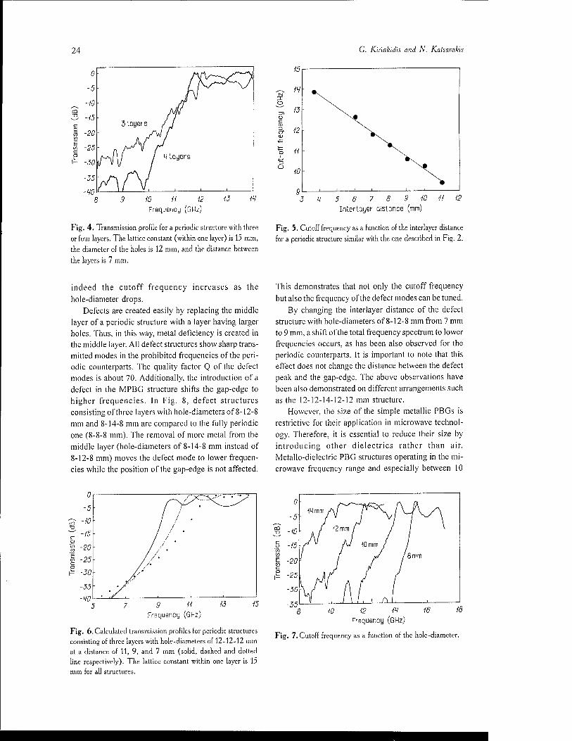
24 C. Kiriakidis and N. Kalsarakis
H
8 9 10 11 12 Frequency (GHz)
Fig. 4. Transmission profile for a periodic structure with three
or four layers. The lattice constant (within one layer) is 15 mm,
the diameter of the holes is 12 mm, and the distance between
the layers is 7 mm.
o
3 15 6 7 8 9 10 11 Interlayer distance (mm)
Fig. 5. Cutoff frequency as a function of the interlayer distance
for a periodic structure similar with the one described in Fig. 2.
indeed the cutoff frequency increases as the
hole-diameter drops. Defects are created easily by replacing the middle
layer of a periodic structure with a layer having larger holes. Thus, in this way, metal deficiency is created in the middle layer. All defect structures show sharp trans- mitted modes in the prohibited frequencies of the peri- odic counterparts. The quality factor Q of the defect modes is about 70. Additionally, the introduction of a defect in the MPBG structure shifts the gap-edge to higher frequencies. In Fig. 8, defect structures consisting of three layers with hole-diameters of 8-12-8 mm and 8-14-8 mm are compared to the fully periodic one (8-8-8 mm). The removal of more metal from the middle layer (hole-diameters of 8-14-8 mm instead of 8-12-8 mm) moves the defect mode to lower frequen- cies while the position of the gap-edge is not affected.
This demonstrates that not only the cutoff frequency
but also the frequency of the defect modes can be tuned. By changing the interlayer distance of the defect
structure with hole-diameters of 8-12-8 mm from 7 mm to 9 mm, a shift of the total frequency spectrum to lower frequencies occurs, as has been also observed for the periodic counterparts. It is important to note that this effect does not change the distance between the defect peak and the gap-edge. The above observations have been also demonstrated on different arrangements such as the 12-12-14-12-12 mm structure.
However, the size of the simple metallic PBGs is restrictive for their application in microwave technol- ogy. Therefore, it is essential to reduce their size by introducing other dielectrics rather than air. Metallo-dielectric PBG structures operating in the mi- crowave frequency range and especially between 10
CD
9 11 Frequency (GHz)
13
Fig. 6. Calculated transmission profiles for periodic structures consisting of three layers with hole-diameters of 12-12-12 mm at a distance of 11, 9, and 7 mm (solid, dashed and dotted line respectively). The lattice constant within one layer is 15 mm for all structures.
0 ■
-5 IM mm
-10 12 mm /
-15 10 mm /
20 - /8 mm
25 -
30 \ f .A /.i A 1, 10 12 11
Frequency (GHz) 16 18
Fig. 7. Cutoff frequency as a function of the hole-diameter.
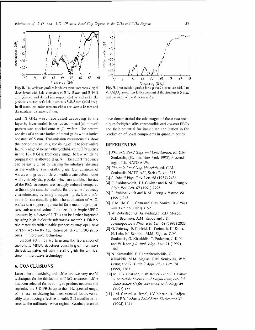
Fabrication of 2-D and 3-D Photonic Band-Gap Crystals in the GHz and THz Regions 25
CG
13 m 15 Frequency (GHz)
Fig. 8. Transmission profiles for defect structures consisting of
three layers with hole-diameters of 8-12-8 mm and 8-14-8
mm (dashed and dotted line respectively) as well as for the
periodic structure with hole-diameters 8-8-8 mm (solid line). In all cases, the lattice constant within one layer is 15 mm and
the interlayer distance is 7 mm.
and 18 GHz were fabricated according to the layer-by-layer model. In particular, a metal (aluminum) pattern was applied onto A1203 wafers. The pattern consists of a square lattice of metal grids with a lattice constant of 5 mm. Transmission measurements show that periodic structures, consisting of up to four wafers laterally aligned to each other, exhibit a cutoff frequency in the 10-18 GHz frequency range, below which no propagation is allowed (Fig. 9). The cutoff frequency can be easily tuned by varying the interlayer distance or the width of the metallic grids. Combinations of wafers with grids of different width create defect modes with relatively sharp peaks, which are tunable. The size of the PBG structures was strongly reduced compared to the simple metallic meshes, for the same frequency characteristics, by using a supporting dielectric sub- strate for the metallic grids. The application of A1203
wafers as a supporting material for a metallic grid pat- tern leads to a reduction of the size of the simple MPBG structure by a factor of 3. This can be further improved by using high dielectric microwave materials. Dielec- tric materials with tunable properties may open new perspectives for the application of "clever" PBG struc- tures in microwave technology.
Recent activities are targeting the fabrication of monolithic MPBG structures consisting of microwave dielectrics patterned with metallic grids for applica- tions in microwave technology.
6. CONCLUSIONS
Laser micro-machining and LIGA are two very useful techniques for the fabrication of PBG structures. LIGA has been selected for its ability to produce accurate and reproducible 3-D PBGs up to the THz spectra! range, while laser machining has been selected for its versa- tility to producing effective tuneable 2-D metallic struc- tures in the millimeter wave regime. Results presented
10 It 13 m 15 Frequency (GHz)
Fig. 9.Transmission profile for a periodic structure with four
Al/Al O layers. The lattice constant of the structure is 5 mm,
and the width of the Al wires is 2 mm.
have demonstrated the advantages of these two tech- niques for high quality, reproducible and low-cost PBGs and their potential for immediate application in the production of novel components in quantum optics.
REFERENCES
[I] Photonic Band Gaps and Localization, ed. CM. Soukoulis, (Plenum: New York 1993), Proceed- ings of the NATO ARW.
[2] Photonic Band Gap Materials, ed. CM. Soukoulis, NATO ASI, Series E, vol. 315.
[3] S. John // Phys. Rev. Lett. 58 (1987) 2486. [4] E. Yablonovitch, T.J. Gmitter and K.M. Leung //
Phys. Rev. Lett. 67 (1991) 2295. [5] E. Yablonovitch and K.M. Leung // Nature 351
(1991)278. [6] K.M. Ho, C.T. Chan and CM. Soukoulis // Phys.
Rev. Lett. 65(1990)3152. [7] W. Robertson, G. Arjavalingan, R.D. Meade,
K.D. Brommer, A.M. Rappe and J.D. Joannopoulos // Phys. Rev. Lett. 68 (1992) 2023.
[8] G. Feiertag, E. Ehrfeld, H. Freimuth, H. Kolle, H. Lehr, M. Schmidt, M.M. Sigalas, CM. Soukoulis, G. Kiriakidis, T. Pedersen, J. Kuhl and W. Koenig // Appl. Phys. Lett. 71 (1997) 1441.
[9] N. Katsarakis, E. Chatzitheodoridis, G. Kiriakidis, M.M. Sigalas, CM. Soukoulis, W.Y. Leung and G. Tuttle // Appl. Phys. Lett. 74 (1999)3263.
[10] M.D.B. Charlton, S.W. Roberts and G.J. Parker // Materials Science and Engineering B-Solid State Materials for Advanced Technology 49 (1997) 155.
[II] J.M. Gerard, A. Izrael, J.Y. Marzin, R. Padjen and F.R. Ladan // Solid State Electronics 37 (1994) 1341.

26 C. Kiriakidis and N. Katsarakis
[12] T. Krauss, Y.P. Song, S. Thorns, C.D.W. Wilkinson and R.M. Delarue // Electronic
Letters 30 (1994) 1444. [13] V. Berger, O. Gauthier Lafaye and E. Costard //
Electronic Letters 33 (1997) 425. [14] R.D. Meade, K.D. Brommer, A.M. Rappe and
J.D. Joannopoulos II Appl. Phys. Lett. 61 (1992)
495. [15] D. Cassagne, C. Jouanin and D. Bertho // Phys.
Rev. B 53 (1996) 7134. [16] H.W. Lau, G.J. Parker, R. Greef and M.
Hoelling // Appl. Phys. Lett. 67 (1995) 1877. [17] D. Labilloy, H. Benisty, C. Weisbuch, T.F.
Krauss, R.M. Delarue, V. Bardinal, R. Houdre,
U. Oesterle, D. Cassagne and C. Jouanin // Phys. Rev. Lett. 79 (1997) 4147.
[18] T.F. Krauss, B. Vogele, C.R. Stanley and R.M. Delarue // IEEE Photonics Technology Letters 9
(1997) 176. [19] C.T Chan, K.M. Ho and CM. Soukoulis //
Europhys. Lett. 16(1991)563. [20] J.G. Fleming and S.Y. Lin // Optics Letters 24
(1999)49. [21] W. Ehrfeld and H. Lehr // Radial. Phys. Chem.
45(1995)349. [22] F.J. Pantenburg and J. Mohr // Nuclear
Instruments and Methods in Physics Research B 97(1995)551.

Mater.Phys.Mech.l (2000)27-30
A MATHEMATICAL MODEL OF METAL FILMS DEPOSITION FROM PHOTOACTIVE COMPOUND
SOLUTIONS ON SOLID-LIQUID INTERFACE
S.A. Kukushkin and S.V. Nemenat
Institute of Problems of Mechanical Engineering, RAS, Vas. Ostrov, Bolshoj pr. 61, 199178, St-Petersburg, Russia
ReceivectOctober 18, 1999
Abstract. The kinetics of the growth of thin metal films from solutions of photoactive chemical coordination compounds irradiated by light at a certain wavelength has been theoretically investigated. In the framework of our mathematical model the time dependencies of the basic characteristics of the film growth process (size distribution function, density of nucleation, concentration of metal on the surface) have been computed. They proved to be in accordance with the experimental data. It is shown that the flux of metal (substance) from the solution onto the surface of the substrate can be derived from the stationary diffusion equation with the added term taking into account the influence of the photochemical substance source. It may be inferred that the variation of light intensity, in great range, keeps the kinetics of the process of film deposition out of the drastic changes.
1. INTRODUCTION
The processes of metal films formation and growth on solid substrates are of great importance from both theo- retical and practical viewpoints [1]. In the papers [2- 5], the process of obtaining Ag, Au, Cu films on flat quartz substrates in the solutions of photoactive chemical coordination compounds was investigated experimentally. The essence of this method is the fol- lowing. Let us consider a solution of the coordination compound [Af'Li)Xm , where M" is the central metal atom (z+ is the oxidation level); L denotes innersphere ligands; X denotes outersphere counterions. If ligand to metal charge transfer ( L-»M ) occurs in this compound, the irradiation of solution by light at the wavelength X = A. results in the reduction of the metal atom. By carrying the irradiation on, the central metal atom can be reducted to the zeroth valence state. Thus, we can write the scheme of the entire process as
-» M + L +X~ [M!*Ln]Xm
One should put the substrate to be deposited on the bottom of the vessel filled with the solution. If we di- rect a light beam from above, its intensity decreases according to the Lambert-Buger-Behr law (Fig. 1).
Zeroth valence metal atoms generated by light will dif- fuse towards the substrate and be adsorbed on it. When the critical concenteration of metal on the substrate surface is reached, the growth of new crystal metal phase starts.
It was noted in [2-5], that the essential feature of films obtained in this way is the narrow size distribu- tion of grains in the film. In those papers, on the basis of the Volmer-Weber theory [6] the qualitative expla- nation of results was proposed. The process of forma- tion and growth of a new phase on the surface is the complicated multistage one [7], and the Volmer-Weber theory does not provide any exact quantitative descrip- tion.
In our opinion, the method described above is very constructive and interesting for problems of films grow- ing. In this work, we investigated theoretically the time dependencies of the basic characteristics of the grow- ing film, on the basis of modern film growth ideas, presented in the publications [1, 7].
2. FLUX OF METAL ATOMS ONTO THE SUBSTRATE
In this work, the initial stage of the film condensation on the solid substrate was investigated. The substrate is considered to be a homogeneous continuous surface. Thermal effects of crystallization and adsorption are neglected. Passing through the solution, the light in- teracts with molecules of coordination compounds. That results in the formation of zeroth valence metal atoms. The power of metal atoms source is given by
g(x) = Ia<paexp[-ax], (1)
Corresponding author: S.V. Nemenat, e-mail: [email protected]
' 2000 Advanced Study Center Co. Ltd.

28 S.A. Kukushkin and S.V. Nemenal
Y ^
Io
f Y Y Y Y Y
Y Y Y Y Y Y Y
Fig. 1. The scheme of the process of photochemical film
deposition; / — the thickness of the solution layer, 7() — the
incident light intensity.
where IQ is the incident light intensity; a is the absorp- tion coefficient; y is the quantum yield. The absorption coefficient a can be represented by a = 2.3s c fev, where t is the extinction; c , is the concentration of ab- sorbing centres in the solution. Here, we suppose that c , is constant. If the height of solution / (Fig. 1) is small, the probability of the formation of metal clusters in the bulk of solution (homogeneous nucleation) van- ishes. In this case, the flux of metal onto the substrate can be derived from the 1D stationary diffusion equa- tion written by
DAc(x) + g(x) = 0, (2)
where A denotes the Laplacian; D is the diffusion coefficient; the power of source is given by the Eq. 1. We make use of the stationary diffusion equation for the following reasons: 1. the source of metal atoms is stationary 2. we suppose that the characteristic time of photo-
chemical reaction is much less than that of diffu- sion and, i.e. the photochemical reaction is not the ratelimiting stage.
The boundary conditions to the Eq. 2 are
dc
dx
c(l)
= 0, (3)
(4)
It means that the flux of metal into the system at the upper boundary of solution (x=0) misses and the concentration of metal on the surface (x=\) is constant
and equal to c*.
In fact, some average time-dependent concentration of adsorbed atoms on the substrate exceeding c'exists. It is the reduced difference of these concentrations be- ing referred to as the supersaturation
m = c,(t)-e, (5)
that is the driving force for the phase transformation on surface. However, due to the growth is carried out
at room temperature and the solubility of metal is very low, the equilibrium concentration of metal c" is also low. This results in formation of surface metal islands at small supersaturations. Therefore, following [1,7, 8], we assume that the application of the boundary condition (4) is enough satisfactory. By differentiation
of the solution of the Eq. 2 with the boundaiy conditions (3) and (4), we can derive the form of the flux of metal
to the surface
y =/(lp(l-exp(-a/)). (6)
3. METAL ISLANDS FORMATION PROCESSES
According to the paper [7], a process of new phase formation goes through three basic stages. The first stage is the fluctuation formation of new phase nuclei. It is described by the Zeldovich theory, modified for the formation on the surface [7]. During this stage, the stationary flux of nuclei, which are spherical segments, has the form [7]:
/(0 = K(£+l)In(£+l)exp V ln2(£+l)
(7)
where E, is the supersaturation; 6=(G /(ä;7))34TIV, O is
the surface tension; v is the volume per atom in nucleus; K is the proportionality coefficient depending on the duffusion coefficient of adatoms. The time lag is esti-
mated by:
/ =■
-F'\nJW{r,cr) (8)
where n is the number of atoms in critical nucleus; F(n) is the Helmholtz energy of nucleus taking form of a spherical segment; W(n) is the diffusion coefficient in the size space taking into account the probability of random eleminating or joining atoms to nucleus (the fluctuations of nucleus in the size space) [9].
F{nJ = ln(£+l)
(9)

A Mathematical Model of Metal Films Deposition from Photoactive Compound Solutions on Solid-liquid Interface 29
At / > ts the second stage starts. This is the process of formation of new phase islands in the system. This stage is described by the system of equations:
df{n;t) c9(v(n;t)f(n;t)) + =0,
ä dn (10)
where v(n\t) = dn. js the linear rate of nucleus growth, written as
v(n;l) = aZ(t)n~ (11)
where a and m are coefficients depending on the mecha- nism of nuclei growth,
——1= \jdt-k\ \f(n;t)ndndt, (12)
where k is the coefficient depending on the metal un- der investigation. The equation above represents the matter conservation. The equation (10) should be complemented by the initial and boundary conditions [7, 10]
./>;0) = 0, /(«,;/) = v(n; t) „=„ '
(13)
The method of solution of this equations system was developed in the paper [10]. The solution of the system allows us to derive the time dependencies of the basic characteristics of the film growth process: 1. the supersaturation h\(t) is as
£(') = £,■ \ + -t{t)4>t{T{t)) r
(14)
2. the frequency of nuclei formation I{i) is as
expt-T* (0^(7X0)]
3. the size distribution function/(w;/) is as
1 ..±- f(*\ /■(«;/)= n <+l—"' x
k + 1 <
( p{n) t p(n) ^
V at„Z„ at„40 J
»i+i
where the auxiliary function is p(n)
(15)
(16)
3600
Fig. 2. The time dependence of supersaturation on the surface
at different values of the incident light intensity: curve 1 —
102" quantum-m'2-sA; curve 2 — 10w quantum-m'1-^; 3 —
1018 quantum-m^-s4; t — time (s), E,(t) — supersaturation
(non-dimensional quantity).
The formulae (14-16) contain the parameter r - quan- tity, which is inverse with respect to the expansion small parameter. This parameter has the very important prop- erty: F « ncr. All other symbols in these formulae correspond to those in the origin paper [10].
4. RESULTS OF CALCULATIONS AND CONCLUSIONS
Assuming that the growing film is determined by the following constants: 7 = 1020 quantum-rrrus~\"\ = 0.8, a = 50/wl
)/ = 2-10-4/M[2-5],D=10"9/«V,\ = 10"30
m\ c*= 1020 atoms-m-\v = 1 J-m1,k= \,a=W\K = 1032,Tr= 10-2s[ll],5.iu/= 10-"w2, r=298K.
Thus the value of the steady flux (Eq. 6) is 2- 10'8
atoms-m'2s'[. ncr « T = 53. That criterium proves that the solution obtained by the small parameter method sufficiently describes the kinetics of the film growth. The time lag value is ts = 1.8-10'6 s.
The results of calculations are presented in Figs. 2-5.
It is seen from Fig. 4, the size distribution takes the form of a bell. It is the form which is predicted by the theory [1, 7].
We have calculated the time dependencies of the size distribution function, the frequency of nucleation and the supersaturation on the surface at three differ- ent values of the incident light intensity of 1020, 10" and 1018 quantum-mA-s'\ The variation of light inten- sity, in great range, keeps the kinetics of the process of film deposition out of the drastic changes.
m + \
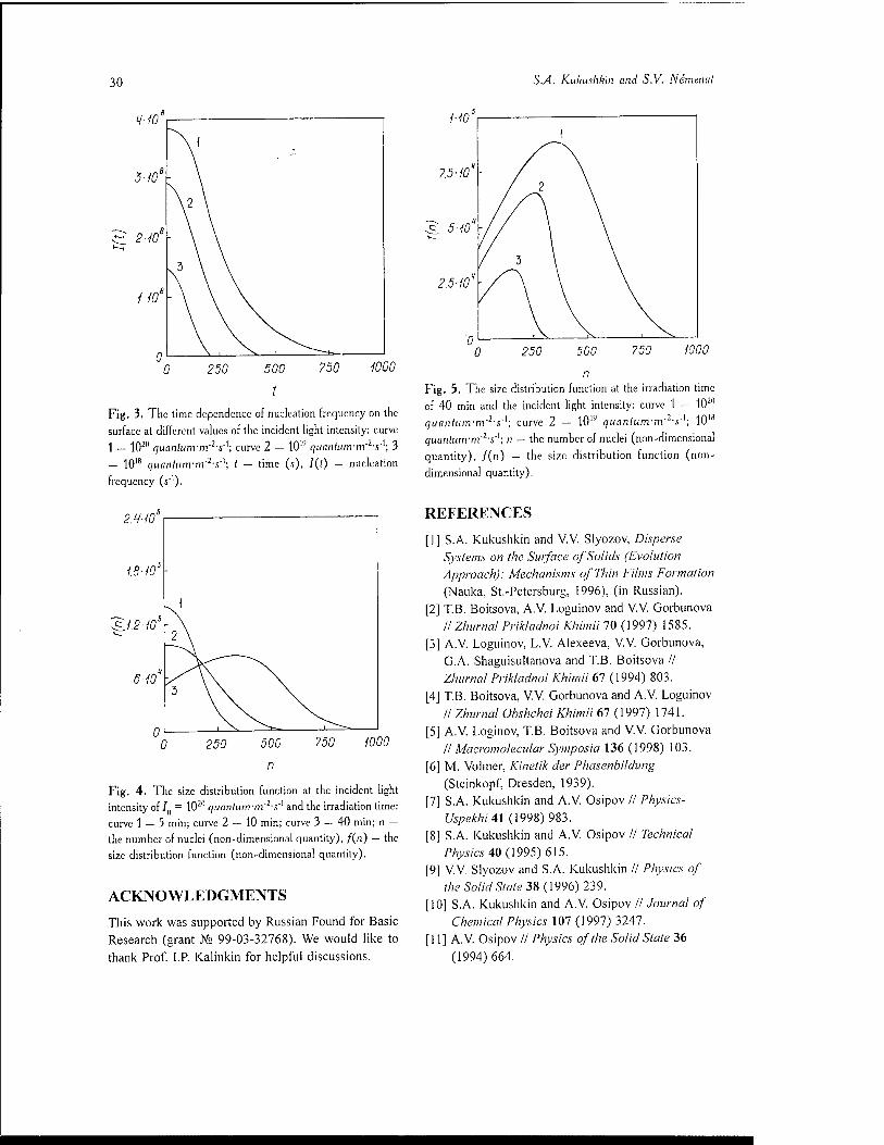
30 S.A. Kukushkin and S.V. Nemenal
V-/0
3-10 -
1-1
1000
Fig. 3. The time dependence of nuclcation frequency on the
surface at different values of the incident light intensity: curve
1 — 102" guan/um-m'V; curve 2 - 10w quantum-m'1-^; 3
— 1018 quanlunrm'2-s'u, t — time (s), /(/) — nuclcation
frequency (s1)-
7.5-10
£ 5-10
2.5-10
1000
Fig. 5. The size distribution function at the irradiation time
of 40 min and the incident light intensity: curve 1 — tO20
quantum-m-2-s'u, curve 2 — 10" quantum-m'1-^; 1018
quantum-m'1-^; n — the number of nuclei (non-dimensional
quantity), /(n) — the size distribution function (non-
dimensional quantity).
2M-10
1.8-10
£1.2-10 -
6-10
1000
Fig. 4. The size distribution function at the incident light intensity of / = 102" quantum-m'2-sA and the irradiation time: curve 1 — 5 min; curve 2 — 10 min; curve 3 — 40 min; n — the number of nuclei (non-dimensional quantity), f(n) — the size distribution function (non-dimensional quantity).
ACKNOWLEDGMENTS
This work was supported by Russian Found for Basic Research (grant Xa 99-03-32768). We would like to thank Prof. I.P. Kalinkin for helpful discussions.
REFERENCES
[I] S.A. Kukushkin and V.V. Slyozov, Disperse Systems on the Surface of Solids (Evolution Approach): Mechanisms of Thin Films Formation (Nauka, St.-Petersburg, 1996), (in Russian).
[2] T.B. Boitsova, A.V. Loguinov and V.V. Gorbunova // Zhurnal Prikladnoi Khimii 70 (1997) 1585.
[3] A.V. Loguinov, L.V Alexeeva, V.V. Gorbunova, G.A. Shaguisultanova and T.B. Boitsova // Zhurnal Prikladnoi Khimii 67 (1994) 803.
[4] T.B. Boitsova, V.V. Gorbunova and A.V. Loguinov // Zhurnal Obshchei Khimii 67 (1997) 1741.
[5] A.V. Loginov, T.B. Boitsova and V.V. Gorbunova // Macromolecular Symposia 136 (1998) 103.
[6] M. Volmer, Kinetik der Phasenbildung (Steinkopf, Dresden, 1939).
[7] S.A. Kukushkin and A.V. Osipov // Physics- Uspekhi 41 (1998)983.
[8] S.A. Kukushkin and A.V. Osipov // Technical Physics 40 (1995) 615.
[9] V.V. Slyozov and S.A. Kukushkin // Physics of the Solid State 38 (1996) 239.
[10] S.A. Kukushkin and A.V. Osipov // Journal of Chemical Physics 107 (1997) 3247.
[II] A.V. Osipov // Physics of the Solid State 36 (1994)664.
Mater.Phys.Mech.l (2000)31-38
ENHANCED DIFFUSION NEAR AMORPHOUS GRAIN BOUNDARIES IN NANOCRYSTALLINE AND
POLYCRYSTALLINE SOLIDS
R.A. Masumura1 and I.A. Ovid'ko2
'Naval Research Laboratory, Washington, DC 20375, USA institute of Problems of Mechanical Engineering,
Russian Academy of Sciences, Bolshoi 61, Vas. Ostrov, St. Petersburg, 199178, Russia
Received: September 23, 1999
Abstract. A theoretical model is constructed that describes diffusion processes enhanced by the elastic interaction of the diffusing species and amorphous grain boundaries in nanocrystalline and polycrystalline solids. A partial differential equation governing evolution of the spatially inhomogeneous concentration of the diffusing species near amorphous grain boundaries is numerically solved. It is shown that the enhanced diffusion essentially influences the growth of amorphous grain boundaries in solids under irradiation and thermal treatment as well in sintered ceramics and is capable of contributing to the anomalously fast diffusion in nanocrystalline solids.
1. INTRODUCTION
The process of the diffusion, where one species rearranges its configuration in a lattice (a solid in this case) in response to an external force, is an attempt to approach equilibrium. When a concentration gradient exists as the only driving force, this irreversible pro- cess can be concisely formulated leading to a second order parabolic partial differential equation (PDE). The solution of this PDE has been determined for many types of boundary and initial conditions and geometries.
If additional driving forces are present due to elec- trical, magnetic, thermal or elastic fields, the appro- priate PDE can be formulated subject to simplifying assumptions. The question now becomes, whether this additional driving force will enhance or retard the flow of diffusing species thorough the lattice. In particular, we are interested in the effect of an amorphous inter- granular boundary dislocation stress field has on the diffusion of various species in nanocrystalline and poly- crystalline solids. Such boundaries frequently exist in sintered nanostructured and polycrystalline ceramics [1-5] as well in monophase and composite solids un- der irradiation and thermal treatment, where diffusion- and irradiation-induced amorphization processes of- ten start to occur at grain boundaries [6,7]. Amorphous grain boundaries in sintered ceramics are characterized by a chemical composition that is different from that of adjacent crystalline grains as well by a nano-scaled
thickness whose value is essentially constant within a ceramic sample. These grain boundaries are dependent on only the chemical composition and insensitive to misorientation parameters of the boundaries (see [1,8] and references therein). Amorphous grain boundaries in monophase and composite solids under irradiation and thermal treatment play the role as nuclei for enhanced diffusion- and irradiation-induced amorphization, where the boundaries transform into extended amorphous layers with the meso- and macro- scale thickness growing parallel with the diffusion and irradiation processes [6,7]. Recently, a model [9,10] has been suggested describing the role of elastic dis- tortions in the formation of amorphous grain bound- aries. This model, however, does not quantitatively take into account the effect of diffusion on evolution of amorphous grain boundaries after they have been formed. At the same time, this effect is important for an adequate description of both the structural features and the properties of nanocrystalline and polycrystal- line solids containing amorphous grain boundaries.
The model presented here is an initial attempt to understand the role of enhanced diffusion in evolution of amorphous grain boundaries in (i) sintered ceram- ics and (ii) monophase and composite solids under irradiation and thermal treatment. The model also is concerned with the contribution of amorphous grain boundaries to enhanced diffusion in nanostructured solids (often exhibiting the outstanding diffusional
Corresponding author: I.A. Ovid'ko, e-mail: [email protected]
2000 Advanced Study Center Co. Ltd.

32 R.A. Mas and I.A. Ovid'ko
properties [11,12]), which is related to elastic interac- tion of amorphous grain boundaries and the diffusing species. As such, we have assumed that the crystalline grains are separated by an amorphous grain boundary layer that provides the source of the diffusing species. To retain the flavor of dislocation model of a simple tilt boundary, we will consider that a double wall of dislocations separate the amorphous layer. We further assume that dislocations do not interact with each other.
We will discuss the development of the appropriate
PDE and the elastic interaction from a double wall of dislocations. This will lead to the formulation of the interaction energy that will be used in the PDE whose solution is determined numerically. Finally, we will discuss the results of the numerical analysis.
2. MATHEMATICAL FORMULATION
The flux or current density of a diffusing species in the
presence of a concentration gradient is given as,
J -DVC, (1)
where D is the diffusivity and C is the concentration. If there is an elastic interaction between the diffusing species and a stress field in a homogenous, linear and isotropic solid, Eq. 1 is modified as [13]
./ = C
DVC+—Vf kT
(2)
where s is the interaction energy, k is Boltzmann's constant and Tis the absolute temperature of the diffu- sion process. It is assumed that the mobility u, caused by the force from the strain gradient is the same as in the chemical potential force,
// = ■
D
kT' (3)
It will be assumed that the diffusivity is constant and independent of both concentration and strain.
Using the continuity equation, Eq. 2 can be recast as
dC , 1 — = D\ V2C+ — VC-Vf ä V kT
since
V2£ = 0>
(4)
(5)
due to the absence of any internal body forces. Eq. 4 along with the appropriate initial and boundary conditions will be solved to determine how the concentration is affected by the elastic interaction.
A formulation for the interaction energy based upon a grain boundary model is required. For nanocrystalline and polycrystalline materials, an appropriate model is the one proposed by Kolesnikova et al. [9] and Ovid'ko and Reizis [10] where an amorphous grain boundary layer occurs as described below between the nanosized
grains.
3. DOUBLE WALL MODEL
In the framework of dislocation-structural-unit mod-
els [14,15], a conventional tilt grain boundary in a crystal can be treated as a periodic wall array of edge grain boundary dislocations whose spatial positions and Burgers vectors are strictly determined by parameters (misorientation, etc.) of the boundary. In this model representation, the elastic fields and the elastic energy
density of a tilt boundary are those of the corresponding
array of grain boundary dislocations [16,17]. Follow-
ing [9,10], transformation of a conventional tilt grain
boundary into an amorphous grain boundary is associ- ated with a re-arrangement of its grain boundary dis-
location ensemble. In doing so, due to the fact that the amorphous disordered structures do not impose strict limitations on both spatial positions and Burgers vec- tors of grain boundary dislocations, such dislocations in a new, amorphous boundary are arranged in the way decreasing their elastic energy density. The discussed decrease of the elastic energy density causes the basic driving force Fel for the transformation of a conventional tilt boundary into an amorphous bound- ary. This force is calculated in the model [9,10] which to a first approximation describes the amorphous boundary to be of finite width, X, with dislocation arrays at each of the interfaces between amorphous and the crystalline grain as shown in Fig. 1. Following the
J. JL
_L -L
-L* jj X J. JL
-> n * -L ■ -L
(a)
.< >.
(b)
Fig. 1. (a) Single dislocation array and (b) double wall with
amorphous grain boundary of width X.

Enhanced Diffusion near Amorphous Grain Boundaries in Nanocrystalline and Polycrystalline Solids 33
calculations of references [9] ^.d [10], the driving force F, is large at X < h, and = 0 at X > A„ where /?, is the period of the dislocation walls (Fig. 1). The elastic in- teraction between the two dislocation walls exists in only the range of X < /?,; the walls, in general, do not interact elastically at X > h2. As a corollary, evolution of the amorphous grain boundary at X - h, is caused by the thermodynamic force F' related to other factors other than the decrease of the elastic energy density.
More precisely, the force F' is as follows [10]:
F'=-£O_C(A)-(2K + ä)- ds
dX (6)
where SIK. denotes the difference between the free energy densities of the amorphous and crystalline phases, and k the characteristic spatial scale of structural inhomogenities in the amorphous phase. The term £ac
strongly depends on the chemical composition which, in general, is spatially inhomogeneous in the vicinity of the amorphous boundary and can evolve in time due to diffusion. In these circumstances, the F'-induced evo- lution of the amorphous grain boundary is sensitive to the diffusion processes in its vicinity. On the other hand, the stress field of the boundary influences the diffusion processes and, as a corollary, evolution of the bound- ary. The elastic interaction between the diffusing spe- cies and the stress field is related to the sum of the normal stresses. For a double wall of non-interacting dislocation infinite arrays a distance X apart the sum of the normal stresses is,
Gb2(\ + v)
2(1 + 1/)/?,
where
®('7>£> =
a>{2n£)
sin(27r£)
(7)
X cosh{2;r(?7 - —)} - cos(2;r£)
2
sin(2;r£)
X cosh{2/r(7/ + —)} - cos(2/r£)
2
(8)
and letting r\ = x/f, , £ =ylh and X" = XIhi for the coordinate system given in Fig. 1 where the disloca- tion walls are symmetrical located at x = ±X/2- The shear modulus and Poisson's ratio are denoted by G and v, respectively.
4. INTERACTION ENERGY
We assume the volume of the diffusing and host spe- cies are different and thus giving rise to an elastic in- teraction. On the average, let A V be the volume change
and this volume difference interacts with a homogenous applied stress field. It can be shown that the elastic interaction is given as
£ = (AV)@, (9)
where © =-c«/3, the hydrostatic component of the stress field. This interaction will alter the total energy of the system depending upon the sign of the product.
In Fig. 2a is plotted the contours of constant normalized interaction energy (i.e., co(r),£)) for a strip |^|<0.5. As expected, a large energy gradient exists near the dislocation, ^=0 due to the elastic singularity of the dislocation core. Depending upon the volume change, this elastic interaction will enhance diffusion. For illustrative purposes, it will be assumed that AK>0. In Fig. 2a, from a qualitative viewpoint, the diffusing species would to migrate below the extra dislocation half plane to lower their total energy. A spherical point defect interacting with a single edge dislocation also exhibits this behavior [18].
The force,/ on the migrating specie is determined from -Vs and the results are shown in Fig. 2b for the corresponding interaction energy of Fig. 2a. The dif- fusing specie will tend to move away from above the dislocation and migrate to the edge of the extra half plane of the dislocation. This periodic case of a tilt boundary is different from that for an isolated edge dislocation in that the diffusing specie in the upper one fourth of the strip diffuses to the next strip above. This is only a qualitative assessment and should serve as guide when a concentration gradient is not considered.
5. NUMERICAL SOLUTION
Before solving Eq. 4, the initial and boundary conditions must be specified. We need to only consider one strip, \b\\ < 1/2, since we assume the grain boundary to be mod- eled by an infinite array of dislocations and can utilize a periodic boundary condition, C(r\,-\/2,t) = C(r|,l/2,/) for r| > 0. We will assume that the amorphous layer in between the nanosized grains will be an undiminished source of the diffusing specie, thus, C(0,h\,t) = 1.0 for \h\\ < 1/2. Since the dislocation stresses from a regular array are short range in nature, it is reasonable to uti- lize C(co,^,;)=0 in each and every strip. The above bound- ary conditions are valid for t> 0. For an initial condition, we will assume that each strip is devoid of any of the diffusing specie at t = 0 leading to C(r|,£,,0) = 0.
Eq. 4 is normalized for computational purposes by rescaling time and letting the material coefficients become
. DGbA\ + v) T = Dt and y= (m
The normalized computational form becomes

34 R.A. Masumura and I.A. Ov'id'ko
Fig. 2(a) shows the normalized interaction energy, CO. Above the dislocation, C0>0 (solid) while below CO<0 (dashed) for
AV>0. The area to the left of the dislocation is one half of the
amorphous layer.
dC_ = v2c + /vc-v&>
with the boundary conditions for t > 0,
C(/7,-l/2,r) = C(;/,l/2,r) for ij > 0,
C(0,£r) = 1.0 for \£\<\/2,
C(oo,£,r) = 0 for |£|<l/2,
and the initial condition at x = 0,
C(?7,4, r) = 0 for JJ > 0 and |£|< 1/2.
(11)
(12)
(13)
(14)
(15)
An alternating-direction-implicit (ADI) method is uti- lized to obtain a numerical solution of Eq. 11. Each time step is divided equally in half. In the first half, a partial solution is determined by reducing the PDE to a one-dimensional problem in one of the orthogonal coordinates while keeping the other fixed. In the sec- ond half, the PDE is now solved in the other coordinate direction using the partial results obtained in the first half time step. This algorithm has the advantage of requiring a tridiagonal equation solver and is relatively stable (unconditionally if the coefficients of the PDE are constant). The redirection partial solution requires a slight modification to the tridiagonal solver to ac- count for periodic nature of the boundary conditions but it still retains the usual banded form. We have chosen to do the analysis first in the redirection since the elastic fields are short-ranged in £.
The finite difference equations are based upon the usual five atom centered-computational molecule to approximate the Laplacian (spatial coordinates) and a two point approximation for the temporal first deriva-
TTTT MM t t t f t t t f t f f / t f /<* t /•»-» f •»
^\\ ^ «- </■ 4 4
\ \ V*-
\ \ W M W
ttu MM MM
TTTTTTTTTTTTTTTT1 t t f t t t t t f /// / Si Si jr
fffftffttttf
//S'Srs>>S>r»S>SS>S'Si
^r,^-*--*-*-».-*--*--*--
WW MM M ii / 4 4 / *s v v /
MM MM
-^-^-K-* ^k. "~*. ~~fc. ~*. ^*. ^*. "^ "~^
WWW ww\
V M V M M M M
4444444J4J44 //////////// *---a- tSf IS IS f V t? V f IS
wwwwww M M M M M M
Fig. 2(b) indicates the flow of diffusant (AV>0)
corresponding to interaction energy shown in Fig. 2a as
determined from -V(0. For clarity, each vector is normalized
to one. The forces away from the dislocation arc greatly
attenuated. The area to the left of the dislocation is one half of
the amorphous layer.
tive. Using equal increments for the spatial coordinates,
A£, = Ar) and utilizing a normalized time increment
Ax, and rescaling y for computation clarity,
/ =4y(A4), (16)
Eq. 12 can be approximated by finite difference form amenable for numerical computation.
For the actual computation, a strip |£ | < 1/2 high and 0 < T] < 3 was used. The grid for this rectangle was divided into 100 and 300 equal increments for the E,- and redirections, respectively. The singularity of stress field was avoided by placing the dislocation in between the grid points. For each time step, the mass accumu- lation, M(t), was determined by numerically integrat- ing the normalized concentration over the computa-
tional rectangle. To check the accuracy of the numerical scheme, an
initial run was made with the interaction set to zero. This case corresponds to diffusion between two planes (one-dimensional problem). These results agreed with the analytical solution lending confidence to the numerical algorithm. Runs were made to explore the effect of the elastic interaction between grain bound- ary dislocations and diffusing species. First was to de- termine the role of the "strength" of the interaction as manifested through y* and second was to determine the effect of spacing between the dislocations (width of amorphous layer) in the wall, X, on the diffusion
process. A typical run for values of y* = 3 and X = 1 is shown
in Fig. 3 for various normalized times. The concentra- tion is larger above the dislocation since the flow lines from Fig. 2a indicate diffusion away from this area

Enhanced Diffusion near Amorphous Grain Boundaries in Nanocryslalline and Polycrystalline Solids 35
T=<00
\\\
I I
T=4500 T = 2500
Fig. 3. Normalized concentration contours for various normalized times with and without elastic interaction. The values of y = 3, A. = 1 and y* = 0, A. = 1 were used. The normalized contours have the same range of values for each time slice. The amorphous layer and other dislocation wall are not shown. The zero interaction case is the smaller segment with the uniform contours.
while the concentration is greatly diminished below the dislocation. The flow pattern generated from the static case, Fig. 2b indicates flow away from the inter- face above the dislocation and flow to the interface below the dislocation due to the elastic interaction. The concentration gradient would prefer to have a uniform flow (no x variation) but cannot overcome the elastic interaction particularly near the singularity at the dis- location. The diffusing specie accumulates below the extra half plane (recall, AV > 0) and diffuses very rapidly to this area due to the mathematical singular- ity. Some the diffusant originates from the strip below as can be seen from the Fig. 2b. However the diffusing specie attempts decreases its concentration in the region above the extra half plane but cannot do so due to its source at the amorphous-crystalline interface. Thus, it flows over a larger area at nearly the maximum concentration in response to the elastic interaction
enhancing the diffusion process. A fraction of the diffusant also flows to the strip above this one.
At later times, the diffusing specie is not effected by the elastic interaction due to the short-ranged effect of the grain boundary dislocation elastic fields. Away from the dislocation, the concentration profile becomes flat indicating a decreased influence of the elastic fields. Note however, at even these later times, the elastic in- teraction near the dislocation remains large as can be seen in Fig. 3. (In Fig. 3, the iso-contour lines have the same range of values for the various time slices.) For comparison, the zero interaction case, y* = 0, is shown in Fig. 3 in the small segment. As expected, the iso- contours are planar for this one-dimensional case. As can been seen from this figure, the iso-contours lines when y* = 0 lag behind the interaction cases and hence affect the mass accumulation of the diffusant.
The presence of the stress field from a grain bound- ary dislocation affects the mass accumulation. In Fig. 4

36 R.A. Ma and I.A. Ovid'ko
1.2
3 F 1.0 -i o o 0.8 V) </> a e 0.6 n CD N OM o £= o Ü.2
^ 5: 0.0
-'T I'" ' i I 1
-A'"
„A"'
A'' Q.D- ° ^A rv- „
o^^ &^Cr rr^i- y» = 0;A = 1.0
o y* = f; A = 0.5 — y» = 1;A = L0 "
d?Jr o y* = 3;A = 0.5
■ t 1
- - y« = 3;A=H.O . a y* = 5; A = 0.5 Y»«=5;X=1.0
/000 2000 3000 W00 5000 6000
T,normalized time
Fig. 4. Normalized mass accumulation for several values of y
and X.
S 1.2 3 1 to O Ü ° 0.8 CO CO
E 0.6 00
$: 0.0 0 /000 2000 3000 WOO 5000 6000
x, normalized time
Fig. 5. Effect of width of dislocation wall spacing on mass
accumulation.
1 1 1
A = 0.25
I i
A A = 0.5 .-^r = 5'0~ A=1.0 *
&- -4r=w. -X-*' ~- '£y~**~*^
-■A .'A K>&'
, "A" ■rfJ* " .'ts ^£r -----A =0.1
o A = 0.5 A - \ 0
if ■id
i i i i '
is plotted the mass accumulation for several
combinations of y* = 0, 1,3 and 5 and X = 0.5 and 1.
There are several salient features to note. First, as ex-
pected, the amount of mass diffusion is increases with
increasing elastic interaction, i.e., larger y*. Second there is very little discernable difference between X =
0.5 and X = 1 indicating that the short-range field ef- fects are limited at these widths. Third, there is an enhanced diffusion over the base line case of y* = 0 of the order of 20% at the later times. Given the little effect of 1 on the mass diffusion, the baseline results for y* = 0.5 or 1 should be about the same. For that reason, we have shown only X = 1 for y* = 0.
The width effect, e.g., the spacing between the dis- location walls has a marginal effect as the spacing, X, becomes smaller. In Fig. 5, X is varied from 0.1, 0.5 and 1 for two values of y = 1 and 5. There is a slight increase in mass accumulation as the width is decreased to a value of 0.1 (recall this means that the spacing of the dislocation in each wall or array is 10 time larger that the separation distance between the walls). This analysis should be treated only as an indication of ef- fect of the elastic interaction because this analysis uses the assumption of non-interacting dislocations.
4. DISCUSSION
We discuss the evolution of amorphous grain bound- aries in (i) sintered ceramics and (ii) solids under irradiation and thermal treatment based on the role of enhanced diffusion. To do so, we assume that the spe- cies diffusing from a pre-existent amorphous grain boundary into adjacent crystalline regions are capable of inducing the amorphization of these regions. This corresponds to experimentally observed situations (i) [1-5] and (ii) [6,7] where diffusion mixing causes growth of the amorphous phase at grain boundaries. With the above taken into account, the following sce- nario of the evolution is suggested which takes into
consideration the role of enhanced diffusion in
amorphizing transformations at grain boundaries. Pen-
etration of the "amorphizing" diffusing species from
an amorphous grain boundary to adjacent crystalline
regions occurs in a spatially inhomogeneous way (see
previous sections and Fig. 6a) and leads to change of 6 in the regions with a high density of the amorphizing diffusing species. This induces amorphization (crystal-to-glass transition) in these regions (Fig. 6b). The spatially inhomogeneous growth of the amorphous phase (Fig. 6b) forces crystalline- amorphous interface to be curved and, therefore, results in an increase of its contribution to the total energy density of the amorphous boundary. The crystalline- amorphous interface can straighten out and, as a corollary, decrease the total energy density in the fol- lowing two-step way. First, grain boundary dislocations, due to absence of structure-imposed limitations on their spatial positions, move to new positions (Fig. 6c). The dislocations located in new positions create a new stress
(O) (b) (c)
A/2 + 6A
(d) (e) Fig. 6. Increased width of layer, 8k, by amorphization due to
enhanced diffusion.
Enhanced Diffusion near Amorphous Grain Boundaries in Nanocrystalline and Polycryslalline Solids 37
field distribution which, in its turn, enhances penetra- tion of the amorphizing diffusing species from the amorphous grain boundary to new crystalline regions located between the "bugles" of the boundary (Fig. 6d). The diffusion is followed by amorphization of these new regions, in which case the crystal/glass interface becomes planar (Fig. 6e).
If there is a permanent "supply" of the amorphizing
diffusing species to the amorphous grain boundary due
to grain boundary diffusion (which quickly transfers the amorphizing diffusing species from some remote permanent source, e.g. a second phase region consisting of chemical elements that serve as the amorphizing diffusing species) or irradiation (see situation (ii)), then the boundary plays the role as a permanent source of the amorphizing diffusing species that penetrate into the adjacent crystalline grains. In these circumstances, the process shown in Fig. 6 is permanently repeated resulting in diffusion- or irradiation-induced perma- nent growth of the amorphous grain boundary. This corresponds to experimentally observed [6,7] situation (ii) where the diffusion- and irradiation-induced growth of the amorphous phase starts occurring at grain bound- aries, which then gradually extend to amorphous regions of macro-scale extent.
If the quantity of the amorphizing diffusing species is limited, as in situation (i) with sintered ceramics, the process shown in Fig. 6 results in formation of an amorphous boundary of finite width. The boundary width is determined only by the sum (finite) quantity of the amorphizing diffusing in a sample. Since grain boundary diffusion is faster by several orders than bulk diffusion (that controls the growth of amorphous grain boundaries; see Fig. 6), basically, the same quantities of the amorphizing diffusing species are distributed along all the grain boundaries within a sample. This explains the experimentally observed (see [1,8] and references therein) specific feature of amorphous grain boundaries in sintered ceramics, which is a finite bound- ary width whose value is tentatively the same for all amorphous grain boundaries within a ceramic sample and depends on only the chemical composition.
The diffusion processes enhanced due to the elastic interaction of the diffusing species and amorphous grain boundaries represent an example of diffusion processes dependent on stress field distributions in polycrystal- line and nanocrystalline solids. The contribution of such processes to the macroscopic diffusional properties is significant in solids with evolving defect structures and, therefore, evolving stress field distributions. In particu- lar, the enhanced diffusion which accompanies trans- formations of amorphous grain boundaries (Fig. 6) is capable of essentially contributing to the anomalously fast diffusion in nanocrystalline solids where evolving
(amorphous and conventional) grain boundaries are
inherent structural elements.
4. CONCLUSIONS
As an initial to attempt to under the role of grain bound- aries and their effect in nanosized materials, we have modeled a simple case of two non-interacting grain boundary arrays or walls separating an amorphous layer
that provides a source for the diffusing species. A simple elastic interaction is considered and inserted into the diffusion equation that is solved for the time depen- dent behavior of the concentration. The mass accumu- lation is enhanced due to the elastic interaction and that until the spacing becomes small, the second dislo- cation array or wall has a minimal effect. And lastly, the static information derived from the interaction energy and its gradient, e.g. force on the diffusing specie, will only yield qualitative information and that
time dependent analysis is required. The enhanced dif- fusion essentially influences the growth of amorphous grain boundaries in solids under irradiation and ther- mal treatment as well in sintered ceramics and is capable of contributing to the anomalously fast diffu- sion in nanocrystalline materials.
ACKNOWLEDGEMENTS
We wish to thank the Office of Naval Research Headquaters (ONR) and Office of Naval Research In- ternational Research Field - Europe (ONR-Europe) for their generous support. One of us, (I.A.O.) was the recepient of ONR grant N00014-99-1-0569) and of ONR-Europe grant N00014-99-1-4016. The other au- thor, (R.A.M.), was supported by ONR grant N0001499AF00002.
REFERENCES
[1] Y.Kinemuchi, T.Yanai and K.Ishizaki // Nanostr.
Mater. 9 (1997) 23. [2] X.Pan // J. Am. Ceram. Soc. 79 (1997) 2975. [3] H.Gu, X.Pan, I.Tanaka, R.M.Cannon,
M.J.Hoffmann, H. Mullejans and M.Ruhle // Mater. Sei. Forum 207-209 (1996) 729.
[4] X.Pan, M.Ruhle and K.Nihara // Mater. Sei. Forum 207-209 (1996) 761.
[5] H.-J.Kleebe, G.Pezzotti and T.Nishida // J. Mater. Sei. Lett. 16(1997)453.
[6] M.A.Hollanders, B.J.Thijsse and E.J.Mittenmejer // Phys. Rev. B 42 (1990) 5481.
[7] W.L.Gong, L.M.Wang and R.C.Ewing // J. Appl.
Phys. 81 (1997)2570. [8] D.R.Clarke II J. Am. Ceram. Soc. 70 (1987) 15.
38 R.A. Masumura and I.A. Ou'id'ko
[9] A.L.Kolesnikova, I.A.Ovid'ko and A.B.Reizis // [14] J. Mater. Proc. Mamif. Sei. 7 (1999) 5.
[10] I.A.Ovid'ko and A.B.Reizis //./. Phys. D: Appl. [15]
Phys. 32(1999)2833. [11] J.Horvath // Defects and Diffusion Forum 66-69
(1989)207. [16] [12] H.-J.Hofier, H.Hahn and R.S.Averback //
Defects and Diffusion Forum 75(1991)195. [17] [13] L.A. Girifalco and D.O. Welch, Point Defects
and Diffusion in Strained Metals (Gordon and [ 18]
Breach, 1967).
A.P.Sutton and V.Vitek // Phil. Trans. Roy. Soc.
London A 301 (1983) 1. A.RSutton and R.W.Ballufi, Interfaces in Crystalline Materials (Clarendon Press, Oxford,
1995). G.-J.Wang and V.Vitek // Ada Metall. 34
(1986)951. K.N.Mikaelyan, I.A.Ovid'ko and A.E.Romanov // Mater. Sei. Eng. A 259 (1999) 132. F.R.N. Nabarro, Theory of Crystal Dislocations
(Clarendon Press, Oxford, 1967).
Mater.Phys.Mech.l (2000) 39-44
CORRELATION BETWEEN SUPERCONDUCTING TRANSPORT PROPERTIES AND GRAIN BOUNDARY MICROSTRUCTURE IN
HIGH-T SUPERCONDUCTING CERAMICS
T.S. Orlova1, J.Y. Laval2 and B.I. Smirnov1
'A.F. Ioffc Physico-Technical Institute, Russian Academy of Sciences, Polytechnicheskaya 26, 194021 St.Petersburg, Russia,
2Laboratoire de Physique du Solide, CNRS ESPCI, 10 rue Vauquelin, 75231 Paris Cedex 05, France
Received: October 21, 1999
Abstract.Thc superconducting transport properties {l-V, I-B and I-T) were correlated with a systematic characterization of the grain boundary microstructurc, via TEM observation and local chemical analysis in STEM by EDX on YBa,Cu3_ Ov (D samples), YBa,Cu3. Ov/AgN (S samples) and DyBa2Cu3.sOv/hvt% Pt (0<x<0.4) ceramics. It was shown that in all samples studied the critical current /. is controlled by weak links at grain boundaries. The measurements of/(7) indicated that in copper-deficient yttrium ceramics, Ag-doping leads to change of weak link character from supcrconductor-insulator-superconductor (SIS) to superconductor-normal mctal-supcrconductor (SNS) type. This SNS behaviour seems to be a result of percolation path of supercurrent through clean boundaries with extremely narrow range (si nm) of Ag segregation on them. Specific Ag precipitates of 2-5 nm size on or near clean boundaries were found in S samples for x=0.4. This is most likely to be a reason for the improvement of/, in these samples by a factor of 3. In copper-deficient dysprosium ceramics doped with Pt, Pt-doping leads to a substantial increase in / and pronounced 'fish-tail' effect in magnetic field at 7"<77 K in non-stoichiometric composition with JC=0.2. Better behaviour of/, in magnetic fields in these samples may be associated with the substantial increase in the proportion of clean boundaries and decrease in twin spacing.
1. INTRODUCTION
In the high-7 granular superconductors, transport properties are mainly controlled by the grain boundary microstructure unlike T which is determined by the crystal structure and oxygen content. Depending on crystallography and structure of boundaries, they can be favourable for the passage of supercurrent or can be weak links (reduced / regions) in the superconducting current path of a ceramic sample. Recently many stud- ies have been directed at investigating the dissipation at a separate boundary of different type [1]. Although studies of separate boundary behaviour highly contribute to understanding transport in superconduct- ing polycrystalline materials, they are rather idealistic models of true polycrystalline materials which contain many boundaries of different types, in parallel and se- ries, simultaneously. So, along with the study of a sepa- rate boundary, it is also very important to investigate the relation between transport properties and grain boundary behaviour as a network of boundaries.
The main aim of this work was to find possible correlation between microstructure features and super- conducting transport properties. One way for changing intergrain critical current density of polycrystalline materials is doping with different elements. Small de- viation from the stoichiometric composition can also lead to a change in structure and distribution of bound- aries in a ceramic sample.
So, in this work the superconducting transport prop- erties (l-V, I-B and I-T) were correlated with a sys- tematic characterization of the grain boundary micro- structure, via TEM observation and local chemical analysis in STEM by EDX. The following supercon- ducting ceramics were studied. 1. YBa2Cu3 xO (0<x<0.4) - Cu-deficient yttrium ce-
ramics (D samples); YBa2Cu3 sO /Agx (0<x<0.4) ce- ramics with silver incorporated in amounts equal to the copper deficiency (S samples).
2. DyBa2Cu3xOy/lwt% Pt (0<x<0.4) - Cu-deficient dysprosium ceramics doped with 1 wt% Pt.
Corresponding author: T.S. Orlova; e-mail: [email protected]
© 2000 Advanced Study Center Co. Ltd.

40 T.S. Orlova et al
2. EXPERIMENTAL
The YBCO ceramic system was fabricated via the modi- fied citrate gel process [2]. The sol-gel method allows one to achieve highly homogeneous mixing of cations on an atomic scale and produce high-quality powder. Two types of YBCO samples were prepared. In samples of the first type YBa2Cu3 xOy (0<x<0.4) (D type) Cu- deficient compositions were obtained. In samples of the second type, YBa7Cu, xOy/Agx (0<x<0.4) (substituted S type), Ag was considered as a substituent for Cu.
The copper deficient ceramics, DyBa2Cu3 Oy, doped by lwt.% Pt, were prepared by the usual solid state reaction. For comparison two compositions with x=0 and x=0.2 of the copper deficient ceramics DyBa2Cu3 xOy
without Pt were also fabricated using the same method. The phase were characterised by powder X-ray dif-
fraction (XRD) using a Philips automated X-ray diffractometer. Microstructure and chemical
compositions were analysed with a Jeol 2000 FX TEM equipped with a Link EXL X-ray selective analyser and with an SEM equipped with an EDAX X-ray se-
lective analyser. The superconducting properties were studied by
measuring the resistivity-temperature (R-T) and current-voltage (/-K) characteristics using the four- probe technique. The critical current /. was determined at various temperatures using the 1 uV-mnr' criterion, with and without external magnetic field B. The exter- nal magnetic field ranged from 0 to 75 G and was per- pendicular to the transport current.
3. RESULTS AND DISCUSSION
3.1 COPPER DEFICIENT YTTRIUM SYSTEM
WITH AND WITHOUT AG-DOPING
First we will consider 123-yttrium system with copper deficiency with and without Ag-doping. According to the data in the literature [3-5] distribution of Ag in ceramics and its influence on ./ are subject to contra- dictory conclusions and strongly depend on composition of ceramics, processing technology and thermal treat- ment. Our ceramic samples were prepared via the modi- fied citrate gel process [2] which allows one to achieve highly homogeneous mixing of cations on an atomic scale and produce high-quality homogeneous ceram-
ics. EDX analysis in TEM showed (Table 1) that the
Ag content (x) of YBCO grains was lower than the nominal amount of Ag, in spite of the sol-gel method. Ag mainly precipitated as small particles (1-2 urn) homogeneously scattered throughout the sample.
Table 1. Average concentration of silver in the grains measured by EDX in TEM and STEM for
YBa,Cu, O /Ag for all doping levels. L i-x y x
Nominal Ag concentration x Real Ag concentration
0.1
0.2
0.4
< limit of detection
<0.02
0.03
X-ray diffraction and SEM analysis showed that all samples had an good orthorhombic structure. For samples with x>0.2, along with Ag phase (S samples) several nonsuperconducting phases such as Y,BaCu05
(211), BaCu02 (011) and CuO (D and S samples) were registrated. The amount of these nonsuperconducting phases (in D and S samples) and Ag-phase (S samples)
increased with increasing x. Second phases such as BaCu02 and CuO were mainly located at grain bound- aries and triple junctions. These impurity phases were
about 1-3 urn in size, the mean distance between them was comparable with respective grain size. The aver- age grain size dramatically decreased with x (Fig. 1). The nonsuperconducting phases and Ag precipitates appear to stop grain growth during sintering resulting in fine-grain microstructure for x>Q2.
For all samples of both type (D and S) the critical temperature was practically the same (7=91-92 K), but the transport properties were quite different. Fig. 2 shows the measured values of critical current density J, at 77 K versus x. For S samples, J increased only slightly with increase in Ag content from x=0 to x=0.2, whereas J increased more than threefold (from ,/=50 A/cm2 for x=0 to .7 = 170 A/cm2) for x=0.4. For D samples with „r>0.2, J is = twice that obtained for the stoichiometric composition.
It should be specially noted that in samples of both type (D and S), the obtained /-Kcurves at 77 K exhib- ited a power-low behaviour. /, was strongly depressed
0.0 O.-f
Fig. (D)
0.2
x (mot)
1. Dependence of the average grain size of YBa2Cu3 O^ and YBa2Cu3 O /Agx (S) samples on x.
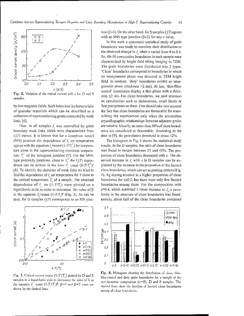
Correlation between Superconducting Transport Properties and Grain Boundary Microstruclure in High-T Superconducting Ceramics 41
160 X / O D
< X S /
c 120 /
/ -°- - ^ / /
/ /
■o
c CD 1_
D 80
/ / o
/ /
^o
O O
Ü un
/ —x— ~~ '
1
/ ^x
I.I. 1
0.0 0/ 0.P 0.J 0 V 05
x (mol) Fig. 2. Variation of the critical current with A- for D and S samples.
by low magnetic fields. Such behaviour is characteristic
of granular materials which can be described as a collection of superconducting grains connected by weak links [6].
Thus, in all samples /. was controlled by grain boundary weak links which were characterized from /.(7) curves. It is known that for a Josephson tunnel (SIS) junction the dependence of/, on temperature agrees with the equation / =const (1-777*) for tempera- ture close to the superconducting transition tempera- ture T of the intergrain junction [7]. For the SNS- type proximity junctions, close to T' the 7(7) depen- dence can be written in the form /=const (\-TIT')
2
[8]. To identify the character of weak links we tried to find the dependence of/ on temperature for T close to the critical temperature Tc of a sample. The obtained dependence of /. on (1-77 7^,) were plotted on a logarithmic scale in order to determine the value of ß in the equation /=const (1-77T)P (Fig. 3). As can be seen, for D samples I (J) corresponds to an SIS junc-
tion (ß~l). On the other hand, for S samples 7.(7) agrees with an SNS type junction (ß«2) for any x value.
In this work a systematic statistical study of grain boundaries was made to correlate their distribution to the observed change in J when x varied from 0 to 0.4. So, 40-50 consecutive boundaries in each sample were characterized by bright field tilting imaging in TEM. The grain boundaries were distributed into 3 types. 'Clean' boundaries correspond to boundaries in which no intergranular phase was detected in TEM bright field. In contrast, 'dirty' boundaries exhibit an inter- granular phase (thickness >2 nm). At last, 'thin-film- coated' boundaries display a thin phase with a thick- ness <2 nm. For clean boundaries, we paid attention on peculiarities such as dislocations, small facets or fine precipitates on them. One should take into account the fact that clean boundaries are favourable for trans- mitting the supercurrent only when the orientation crystallographic relationships between adjacent grains are suitable. Usually, no more than 50% of clean bound- aries are considered as favourable. According to the data in [9], the percolation threshold is about 12%.
The histogram in Fig. 4 shows the statistical study results. In the D samples, the ratio of clean boundaries was found to remain between 27 and 45%. The pro- portion of clean boundaries decreased with x. The ob- served increase in J with x in D samples can be ex- plained by the increase in the proportion of the faceted clean boundaries, which can act as pinning centres (Fig. 4). Ag doping resulted in a higher proportion of clean boundaries for x>0.2, but there were only few faceted boundaries among them. For the composition with *=0.4, which exhibited 3 times increase in J',, a pecu- liarity in the structure of clean boundaries was found, namely, about half of the clean boundaries contained
0.1
0.01
. P=2/ *x
•
/
x / /p=t
/o
^ A^ 0 / A A
• x=0
▼ X=CMS
/ .'^ A A o x=0.2S A x=0.2D
T i
x x=0.MD
0.01 0.1
\-T/Tc
Fig. 3. Critical current versus (1-T/T ) plotted for D and S samples in a logarithmic scale to determine the value of b in the equation / =const (\-T/T)p. ß=l and ß=2 cases are shown by the dashed lines.
-0 X=(HS X=0.2S x=0MS X=0m x=0.2D x=0.MD
Fig. 4. Histogram showing the distribution of clean, thin- film-coated and dirty grain boundaries for a sample of the stoichiometric composition (x=0), D and S samples. The dashed lines show the fraction of faceted clean boundaries among all clean boundaries.

42 T.S. Orlova et al
16 nm
Fig. 5. Micrograph of a 'clean' boundary with Ag precipitates
(shown by arrows) in TEM for an S sample (.v=0.4).
small precipitates of 2-5 nm in size on the boundary
itself, or close to it (up to 5 nm). The average distance
between these precipitates was about 30 nm. An ex-
ample of such a 'clean' boundary with Ag precipitates
is presented in Fig. 5. These small Ag precipitates can
act as very efficient pinning centres resulting most likely in the 3-fold increase in ./ in this composition.
To detect possible Ag segregation at clean grain boundaries, EDX analysis in STEM with 1 nm probe was used. The detected concentration of Ag on some clean boundaries was twice higher than the obtained solubility limit of Ag in the grains (x=0.03). This in- creased Ag segregation on grain boundaries most prob- ably leads to SNS behaviour of weak links in S samples as result of a percolation path of supercurrent through such 'clean' boundaries with an extremely narrow Ag
segregation (=1 nm) on them.
3.2 Cu-DEFICIENT DYSPROSIUM CERAMICS
DOPED WITH 1 wt.% Pt
The next system studied was Cu-deficient dysprosium ceramics doped by Pt. Such a ceramic system was chosen due to the following reason. As we saw above, the deviation from stoichiometry leads to the forma- tion of secondary phases in sintered ceramics. Accord- ing to the literature data [10. 11], in melt-textured ce- ramics the addition of Pt can result in decrease in size of 211 secondary phase inclusions, improving thereby their pinning possibility and. then the critical current. In our work, for Cu-deficient dysprosium sitered ce- ramics doped with Pt. we tried again to identify micro- structural elements, which can be responsible for the differences in superconducting properties.
In all compositions, Pt-doping resulted in the nucle- ation of intragranular secondary phases of submicron
e o
<
150
100
X X
r H.
- .K \
-x- x=0(Pt) —•— x=0
o x=0.l(Pt) -A- x=0.2(Pt) -T- x=0.2
-o- x=0.H(Pt)
50
0 i . i . i . i .
20 10 60 80
B(G)
Fig. 6. Critical current density at 77 K versus applied magnetic field for DyBa,Cu, O/lwt.%Pt and DyBa,Cu, O samples.
size, which contain Pt and were homogeneously dis-
tributed into 123 grains. In addition, in the non-sto-
ichiometric composition, Pt was also located in in-
tergranular BaCu02 secondary phases. Unlike the melt-
textured 123 ceramics [10, 11], no influence of Pt on
size and distribution of 211 secondary phase was found. Traces of Pt in the 123 grains were detected in all compositions doped by Pt. Distribution of Pt in the matrix was inhomogeneous. The maximum content of Pt in a grain was 0.06 molar content.
Fig. 6 displays the dependence of critical current density J on applied magnetic field. As seen, at zero- magnetic field doping with platinum practically does not change J in stoichiometric composition, but leads to its substantial increase for non-stoichiometric composition with x=0.2. The stoichiometric compo- sitions exhibit a sharp drop of J values even in very low magnetic field. Non-stoichiometric compositions show a much smoother decrease in J with magnetic field. Doping with Pt strongly contributed to the so- called 'fish-tail' effect which means stabilization of J in magnetic field. For this composition this 'fish-tail' behaviour became more pronounced when the tempera- ture was decreased (Fig. 7). So, the copper-deficient samples, especially the one doped with Pt seem to have better possibilities for pinning magnetic vortices in applied magnetic fields.
Similar to the system with Ag, for these ceramics with Pt we also tried to identify the character of the intergranular junction network from / versus tempera- ture dependence (Fig. 8). Grain boundary network was found to behave predominantly as SIS junctions, even in Pt-doped samples so that Pt seems not to segregate in sufficient amount, at least, at grain boundaries. Within the accuracy of our EDX analysis we did not reveal higher concentration of Pt in boundaries
compared with grains.
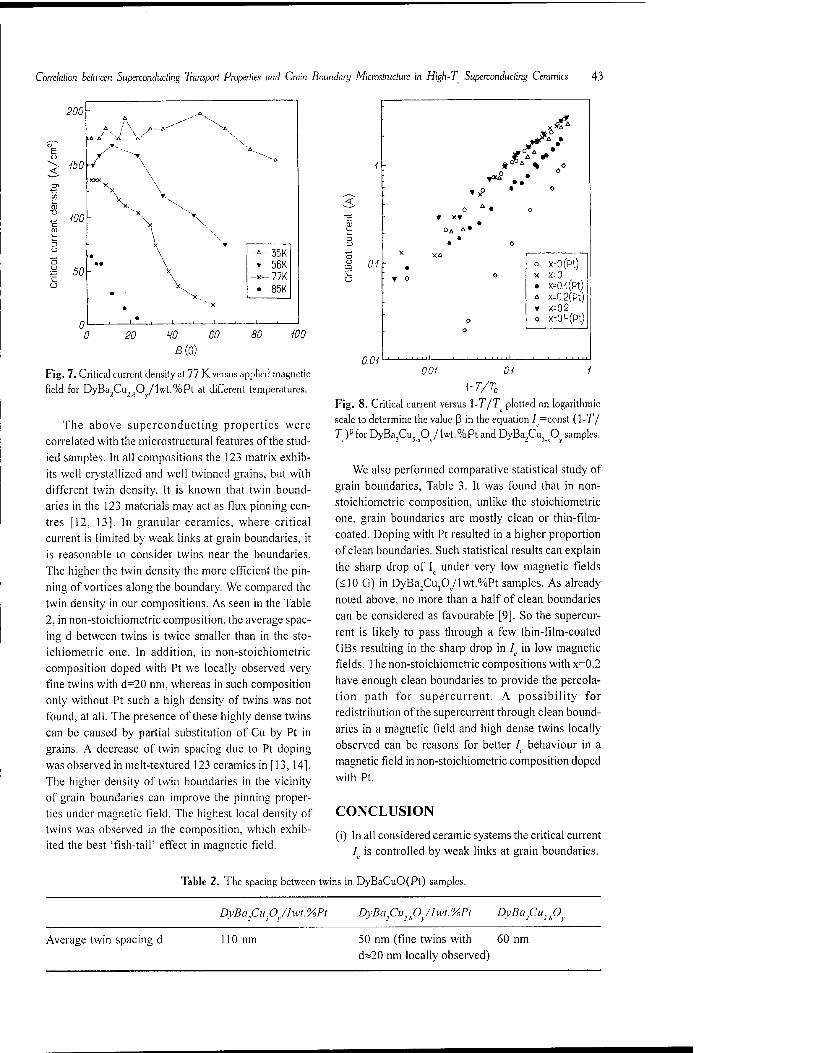
Correlation between Superconducting Transport Properties and Grain Boundary Microstruclure in Hig/i-T Superconducting Ceramics 43
E CJ
<
pon A
A- /\ .^-a"" -" X iA ■£> ~~ü A' \
X
150 **% \
• \ V
^A
V. \ 100 \ X
\ \
\ -a- 35K
V -»- 56K bU
\ X,
-x- 77K • 85K * V
• ~"x
• 1 1 I,I.
20 HO 60
5(G)
80 WO
Fig. field
7. Critical current density at 77 K versus applied magnetic
for DyBa Cu.-O /lwt.%Pt at different temperatures.
The above superconducting properties were correlated with the microstructural features of the stud- ied samples. In all compositions the 123 matrix exhib- its well crystallized and well twinned grains, but with different twin density. It is known that twin bound- aries in the 123 materials may act as flux pinning cen- tres [12, 13]. In granular ceramics, where critical current is limited by weak links at grain boundaries, it is reasonable to consider twins near the boundaries. The higher the twin density the more efficient the pin- ning of vortices along the boundary. We compared the twin density in our compositions. As seen in the Table 2, in non-stoichiometric composition, the average spac- ing d between twins is twice smaller than in the sto- ichiometric one. In addition, in non-stoichiometric composition doped with Pt we locally observed very fine twins with d=20 nm, whereas in such composition only without Pt such a high density of twins was not found, at all. The presence of these highly dense twins can be caused by partial substitution of Cu by Pt in grains. A decrease of twin spacing due to Pt doping was observed in melt-textured 123 ceramics in [13,14]. The higher density of twin boundaries in the vicinity of grain boundaries can improve the pinning proper- ties under magnetic field. The highest local density of twins was observed in the composition, which exhib- ited the best 'fish-tail' effect in magnetic field.
B 0.1
0 *• » XT •
• • 0
**>
* 0° ft 0
o
x XA
• : T 0 o
o
o X=0(Pt) x x=0 • x=0.l(Pt) A x=0.2(Pt) T X--02 o x=O.H(Pt)
I 0.01 001 0.1 1
{-T/Tc
Fig. 8. Critical current versus 1-T/T plotted on logarithmic
scale to determine the value ß in the equation / =const (1-T/
T/ for DyBa2Cu3 Oy/lwt.%Pt and DyBa2Cu3_ Oy samples.
We also performed comparative statistical study of grain boundaries, Table 3. It was found that in non- stoichiometric composition, unlike the stoichiometric one, grain boundaries are mostly clean or thin-film- coated. Doping with Pt resulted in a higher proportion of clean boundaries. Such statistical results can explain the sharp drop of Ic under very low magnetic fields
(<10 G) in DyBa2Cu30 /lwt.%Pt samples. As already noted above, no more than a half of clean boundaries can be considered as favourable [9]. So the supercur- rent is likely to pass through a few thin-film-coated GBs resulting in the sharp drop in / in low magnetic fields. The non-stoichiometric compositions with x=0.2 have enough clean boundaries to provide the percola- tion path for supercurrent. A possibility for redistribution of the supercurrent through clean bound- aries in a magnetic field and high dense twins locally observed can be reasons for better / behaviour in a
c
magnetic field in non-stoichiometric composition doped with Pt.
CONCLUSION
(i) In all considered ceramic systems the critical current I is controlled by weak links at grain boundaries.
Table 2. The spacing between twins in DyBaCuO(Pt) samples.
DyBa,Cu3Oy/lwt%Pt DyBafu,Py/lwt.%Pt DyBafiu^
Average twin spacing d 110 nm 50 nm (fine twins with 60 nm d«20 nm locally observed)

44 T.S. Orlova el al
Table 3. The distribution of clean, thin-film-coated and dirty grain boundaries in DyBa2Cu3_xO /lwt% Pt samples.
DyBafu30 /lwt% Pt DyBafu2sOy/lwt% Pt DyBafu,fiy
Clean 24% Thin-film 16% Dirty 56% Non-characterized 4%
58% 29% 5% 8%
44% 37% 15% 4%
(ii) In Cu-deficient yttrium ceramics doped with Ag in amount equal the deficiency, Ag doping leads to change of type of the weak links from SIS to SNS- type. Such SNS behaviour is a result of percolation path of supercurrent through clean boundaries with extremely narrow (lnm) Ag-segregation on them.
For x=0.4, decoration of clean boundaries by very
fine Ag-precipitates (2-5 nm) is the most likely
reason for 3 fold increase of critical current.
(iii) In non-stoichiometric composition with x=0.2, Pt- doping leads to pronounced increase in Ic and fish-
tail effect in magnetic field. This may be associ- ated with the substantial increase in proportion of clean boundaries and highly dense twins locally observed (due to Pt segregation in 123 grains). No noticeable segregation of Pt in grain boundaries was revealed.
REFERENCES
[1] S.E. Babcock and J.L. Vargas II Annu. Rev. Mater. Sei. 25 (1995) 193.
[2] R.S. Liu, W.N. Wang, C.T. Chang and P.T. Wu // Japan. J. Appl. Phys. 28 (1989) L2155.
[3] D.F. Lee, X. Chaud and K. Salama // Physica C
181 (1991)81.
[4] J. Joo, J.P. Singh, R.B. Poeppel, A. K. Gangopad- hyay and TO. Mason IIJ. Appl. Phys. 71 (1992)
2351. [5] C. Nguyen-van-Huong, E. Crampin, J.Y. Laval
and A. Dubon // Supercond. Sei. Technol. 10
(1997) 85. [6] R.L. Peterson and J.W. Ekin // Physica C 157
(1989)325. [7] J. Jung, I. Isaac and A.-K. Mohamed // Phys.
Rev. 5 48(1993)7526.
[8] P.G. DeGennes // Rev. Mod. Phys. 36 (1964) 225. [9] V.K.S. Shante and S. Kirpatrick // Adv. Phys. 20
(1971)325. [10] M. Murakami, S. Gotoh, N. Koshizuka, S. Tanaka,
T. Matsushita, S. Kanube and K. Kitazama // Cryogenics 30 (1990) 390.
[11] M. Murakami, H. Fujimoto, S. Gotoh, K. Yamagushi, N. Koshizuka and S. Tanaka // Physica C 185-189 (1991) 321.
[12] A.H. King and Y. Zhu // Phil. Mag. A 67 (1993)
1037. [13] I. Monot, K. Verbist, M. Herview, P. Laffez,
M.P. Dalamare, J. Wang, G. Desgardin and G.V
Tendeloo // Physica C 21A (1997) 253. [14] M.P. Delamare, M. Hervieu, J. Wang, J. Provost,
I. Monot, K. Verbist and G.V. Tendeloo // 1996 Physica C 262 (1996) 220.
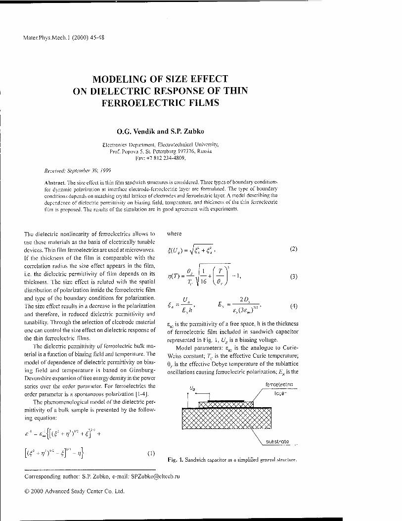
Mater.Phys.Mech.l (2000) 45-48
MODELING OF SIZE EFFECT ON DIELECTRIC RESPONSE OF THIN
FERROELECTRIC FILMS
O.G. Vendik and S.P. Zubko
Electronics Department, Electrotechnical University, Prof. Popova 5, St. Petersburg 197376, Russia
Fax:+7 812 234-4809,
Received: September 30, 1999
Abstract. The size effect in thin film sandwich structures is considered. Three types of boundary conditions for dynamic polarization at interface electrode-ferroelectric layer are formulated. The type of boundary conditions depends on matching crystal lattices of electrodes and ferroelectric layer. A model describing the dependence of dielectric permittivity on biasing field, temperature, and thickness of the thin ferroelectric film is proposed. The results of the simulation are in good agreement with experiments.
The dielectric nonlinearity of ferroelectrics allows to use these materials as the basis of electrically tunable devices. Thin film ferroelectrics are used at microwaves. If the thickness of the film is comparable with the correlation radius the size effect appears in the film, i.e. the dielectric permittivity of film depends on its thickness. The size effect is related with the spatial distribution of polarization inside the ferroelectric film and type of the boundary conditions for polarization. The size effect results in a decrease in the polarization and therefore, in reduced dielectric permittivity and tunability. Through the selection of electrode material one can control the size effect on dielectric response of the thin ferroelectric films.
The dielectric permittivity of ferroelectric bulk ma- terial is a function of biasing field and temperature. The model of dependence of dielectric permittivity on bias- ing field and temperature is based on Ginsburg- Devonshire expansion of free energy density in the power series over the order parameter. For ferroelectrics the order parameter is a spontaneous polarization [1-4].
The phenomenological model of the dielectric per- mittivity of a bulk sample is presented by the follow- ing equation:
where
lit +11 ) (i)
£(£/„) = V£ + £'
im=—J—+ T,. V 16
4* = Eh
£.. =■ 2£>
£S3sJ 3/2 '
(2)
(3)
(4)
E00 is the permittivity of a free space, h is the thickness of ferroelectric film included in sandwich capacitor represented in Fig. 1, UB is a biasing voltage.
Model parameters: s00 is the analogue to Curie- Weiss constant; Tc is the effective Curie temperature; 0 is the effective Debye temperature of the sublattice oscillations causing ferroelectric polarization; EN is the
ferroelectric
Fig. 1. Sandwich capacitor as a simplified general structure.
Corresponding author: S.P. Zubko, e-mail: [email protected]
© 2000 Advanced Study Center Co. Ltd.
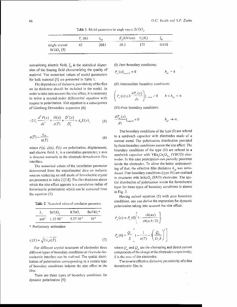
46 O.G. Vendik and S.P. Zubko
Table 1. Model parameters for single crystal SrTi03
?;.(K) £v(kV/cm) 6y,(K) S.v
single crystal
SrTiO, [5]
42 2081 19.3 175 0.018
normalizing electric field; £v is the statistical disper- sion of the biasing field characterizing the quality of material. The numerical values of model parameters for bulk material [5] are presented in Table 1.
The dependence of dielectric permittivity of the film on its thickness should be included in the model. In order to take into account the size effect, it is necessary to solve a second-order differential equation with respect to polarization. This equation is a consequence
of Ginsburg-Devonshire expansion [6]:
dlP{x) D{x) D\x) -2/1, — + + • — = £.fi(x)
clx s(T) D:
£{T) icn
(5)
(6)
where P(x), D(x), E(x) are polarization, displacement, and electric field; \{ is a correlation parameter; x axis is directed normally to the electrode-ferroelectric film interface.
The numerical values of the correlation parameter determined from the experimental data on inelastic neutron scattering on soft mode of ferroelectric crystal are presented in Table 2 [7,8]. The film thickness above which the size effect appears is a correlation radius of ferroelectric polarization which can be extracted from the equation (5).
Table 2. Numerical values of correlation parameter.
X, SrTiO, KTaO, BaTiO*
urn2 1.15-10-7 5.37-10-7 10"'
* Preliminary estimation
r(T) = J2Al£(T). (7)
For different crystal structures of electrodes three different types of boundary conditions at electrode-fer- roelectric interface can be realized. The spatial distri- bution of polarization corresponding to a certain type of boundary conditions induces the size effect in the film.
There are three types of boundary conditions for dynamic polarization [9]:
(I) Zero boundary conditions:
K,=h
(II) Intermediate boundary conditions:
r dP O)^ P (x)±b '"
V dx j 0 h < h „ < co
(III) Free boundary conditions:
dP (x) tic ^ ' I
dx = 0 h —> co
The boundary conditions of the type (I) are refered
to a sandwich capacitor with electrodes made of a normal metal. The polarization distribution provided by these boundary conditions causes the size effect. The boundary conditions of the type (II) are refered in a sandwich capacitor with YBa^Cu^O^ (YBCO) elec- trodes. In this case polarization can partially penetrate inside the electrodes. To allow the better understand- ing of that, the effective film thickness h was intro- duced. Free boundary conditions (type III) are realized in structures with SrRuO, (SRO) electrodes. The spa- tial distribution of polarization inside the ferroelectric layer for three types of boundary conditions is shown
in Fig. 2. Having solved equation (5) with zero boundary
conditions, one can derive the expression for dynamic polarization taking into account the size effect:
P(x)=PJ0) ch(ax)
ch(ah/2)
1(0) s
1-- s{T)
where O and O, are the alternating and direct current components of the charge at the electrodes respectively; 5 is the area of the electrodes.
The inverse effective dielectric permittivity of a thin ferroelectric film is:
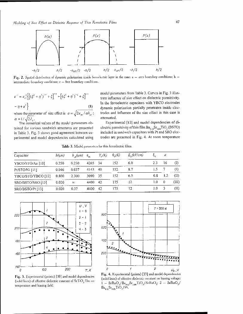
Modeling of Size Effect on Dielectric Response of Thin Ferroelectric Films 47
-h/2
P(x)
—r -r-
/ \ 1
I
\ \ i
h/2 -he«/2 -h/2 h/2 heff/2
Fig. 2. Spatial distribution of dynamic polarization inside ferroelectric layer in the case: a — zero boundary conditions; b
intermediate boundary conditions; c — free boundary conditions.
-V + a) (8)
where the parameter of size effect is a = J2sm I aheff ;
The numerical values of the model parameters ob- tained for various sandwich structures are presented in Table 3. Fig. 3 shows good agreement between ex- perimental and model dependencies calculated using
model parameters from Table 3. Curves in Fig. 3 illus- trate influence of size effect on dielectric permittivity. In the ferroelectric capacitors with YBCO electrodes dynamic polarization partially penetrates inside elec- trodes and influence of the size effect in this case is
attenuated. Experimental [13] and model dependencies of di-
electric permittivity of thin film Ba0 |2Sr08STiO3 (BSTO) included in sandwich capacitors with Pt and SRO elec- trodes are presented in Fig. 4. At room temperature
Table 3. Model parameters for thin ferroelectric films.
Capacitor hfom) hjv-m) eoo TC(K) %(K) EN(kV/cm) Is a
YBCO/STO/Au [10] 0.250 0.230 4265 34 152 6.0 2.3 16 (I)
Pt/STO/Ni [11] 0.046 0.037 4143 40 152 8.7 1.5 7 (I)
YBCO/STO/YBCO [12] 0.800 2.300 3090 35 152 6.5 0.8 1.2 GO SRO/BSTO/SRO[13] 0.020 oo 4400 42 175 12 1.0 0 (III)
SRO/BSTO/Pt[13] 0.020 0.37 4400 42 175 12 1.0 3 (II)
220
200
mo
1B0
w
/ u ,y \ - 0
2
2 - 1
3 - 2
M - 3 —— • -7 • '
J •
• •
0 wo 200 T.K
Fig. 3. Experimental (points) [10] and model dependencies
(solid lines) of effective dielectric constant of SrTi03 film on temperature and biasing field.
800
800
W0
200
I I r=300K
>\
1
2
■*-Sj
0 1 uB,v Fig. 4. Experimental (points) [13] and model dependencies (solid lines) of effective dielectric constant on biasing voltage: 1 - SrRu03/Ba(|12Sr|)88Ti03/SrRu03; 2 - SrRuO,/
Ba„2Sr
U,aTi03/Pt-
48 O.G. Vendik and S.P. Zubko
effective permittivity of the film in capacitor with SRO electrodes is higher than permittivity of single crystal in about 2.5 times. One can conclude that in the case of good matching of crystal lattices of electrodes and ferroelectric film the size effect is suppressed and free boundary conditions for dynamic polarization are realized. Tunability of such capacitor is more better than tunability of the capacitor with Pt electrode.
Thus interface between thin ferroelectric film and electrodes determines distribution of polarization inside ferroelectric layer and therefore variation of dielectric characteristics of sandwich capacitor. By chosen elec- trodes one can suppress size effect in thin film struc-
tures.
REFERENCES
[1] V.L. Ginsburg // Zh. Eksp. Theor. Fiz. 19 (1949)
36. [2] A.F. Devonshire // Phil. Mag. 40 (1949) 1040.
[3] O.G. Vendik // Fiz. Tverd. Tela 14 (1972) 989.
[4] O.G. Vendik and S.P. Zubko II J. Appl. Phys. 82 (1997)4475.
[5] K. Bethe // Philips Research Report, Supplement,
No. 2(1970) 1. [6] O.G. Vendik and L.T. Ter-Martirosyan // Fiz.
Tverd. Tela 36 (1994) 3343. [7] O.G. Vendik and I.G. Mironenko // Fiz. Tverd.
Tela 16 (1974) 3445. [8] S.P.Zubko // Tech. Phys. Lett. 24 (1998) 839. [9] O.G. Vendik, S.P. Zubko and L.T. Ter-Martirosayn
II Appl. Phys. Lett. 73 (1998) 37. [10] F.A. Miranda, C.H. Mueller, G.A. Koepf and
R.M. Yandrofski II Supercond. Sei. Techno/. 8
(1995)755. [11] S. Komatsu and K. Abe // Jpn. J. Appl. Phys. 23
Pt. 1 (1995)3597. [12] A.T. Findikoglu, C. Doughty and S.M. Anlage //
Appl. Phys. Lett. 63 (1993) 3215.
[13] M. Izuha, K. Abe and N. Fukushima // Jpn. J.
Appl. Phys. 36, Pt.l (1997) 5866.

Mater.Phys.Mech.l (2000)49-53
CRITICAL CURRENT DENSITY IN POLYCRYSTALLINE HIGH-TC SUPERCONDUCTORS WITH DISORDERED TILT
BOUNDARIES
S.A. Kukushkin, A.V. Osipov and I.A. Ovid'ko
Institute of Problems of Mechanical Engineering, Russian Academy of Sciences, Bolshoi 61, Vas. Ostrov, St. Petersburg, 199178, Russia
Received: November 18, 1999
Abstract. A theoretical model is suggested which describes the effect of tilt boundaries with chaotically arranged dislocations on the critical current density in high-transition-temperature {T) superconductors. Stress fields of such boundaries, that suppress high-f superconductivity, are revealed to be long-range as compared to those of tilt boundaries with periodically ordered grain boundary dislocations. With this factor taken into consideration, the dependence of the critical current density accross tilt boundaries on boundary misorientation 0 is calculated and compared with the experimental data [1].
1. INTRODUCTION
The transport properties of grain boundaries in high - Tc superconducting materials are the subject of inten- sive theoretical and experimental studies (e.g., see [1- 14]) motivated by extremely large interest to appllications of such materials. It has been experimen- tally revealed that grain boundaries drastically suppress the superconducting critical current [1-3]. In particu- lar, the critical current density, jc, apross tilt bound- aries in YBa2Cu,075 superconductors decreases with boundary misorientation angle 8 as follows :y'c(9)«y'c
(0°)exp(-9/8°), for 9 ranging from 0° to 15°. The critical current density yc(9) across high-angle tilt boundaries with 9 > 15° is tentatively constant and low: y'c(9 >
15o)*0.02ye(0°)[l-3]. Microscopic mechanism of the grain boundary ef-
fect on high-T. superconductivity is not understood yet, though several models of the effect in question have been suggested [5-14]. In particular, theoretical mod- els have been elaborated describing the grain bound- ary effect as that related to the following factors : (i) a decrease of electron free path in vicinities of grain boundaries [6]; (//') stress-field-induced structural dis- order and pinning of magnetic vortices at grain bound- aries [7-9]; (//'/) formation of the antiferromagnetic phase within grain boundary cores [10]; (;'v) faceting of grain boundaries and d -symmetry of the supercon- ducting order parameter [11]; (v) deviations from bulk stoichiometry in vicinities of grain boundaries [12-14].
Most models discussed treat stress fields of grain bound- ary dislocations as those responsible for suppression of the superconducting order parameter in vicinities of grain boundaries in high-f superconductors [7-10]. Though the concrete mechanism of the suppression is not unambigiously recognized yet, many researchers assume the existence of a critical stress, CJC., which characterizes superconductor-to-non-superconductor transition in stressed regions [7-10]. More precisely, superconductivity is supposed to be completely sup- pressed in regions where some component(s) of stress tensor is (are) larger than ac. However, this idea is in contradiction with experimental data in case of low- angle boundaries consisting of periodically arranged lattice dislocations (Fig.la). Actually, for any value of c , the volume fraction of "critically stressed" regions (regions where some component(s) of stress tensor is (are) larger than a.) in vicinities of such low-angle boundaries (that create short- or intermediate-range stress fields which drop as exp(-x/h0), where x denotes the distance from a boundary plane, and h0 the interspacing (period) between periodically arranged dislocations, see (Figs, la and 2a) decreases with boundary misorientation 8.
This, in context of the idea on existence of the critical stress sc, results in increase of the critical current density, j , with boundary misorientation 9, while ex- periments [1-3] are indicative of the fact thaty'c drasti- cally decreases with 9 in the range of 9 from 0° to tentatively 15°. In order to avoid the contradiction dis-
Corresponding author: I.A. Ovid'ko, e-mail: [email protected]
| 2000 Advanced Study Center Co. Ltd.

50 S.A. Kukushkin, A.V. Osipov and I.A. Ovid'ko
(a) (b)
Fig. 1. Ordered and disordered, low-angle tilt boundaries are
represented as (a) periodically ordered and (b) disordered walls
of crystal lattice dislocations of the edge type, respectively.
(a) (b)
Fig. 2. High-angle tilt boundaries with (a) periodically ordered
and (b) disordered ensembles of grain boundary dislocations.
cussed, Gurevich and Pashitskii [10] assume that the non-superconducting, critically stressed regions consist of two, normal metal and antiferromagnetic, phases, in which case the antiferromagnetic phase effectively destroys the coupling of Cooper electrons in vicinities of grain boundaries.
In this paper we suggest an alternative model of the grain boundary effect on high-Tc superconductiv- ity, based on both the idea on critical stress a. and that on disorder in spatial arrangement of grain boundary dislocations in high-T superconductors. Actually, high- T superconducting materials commonly are synthe- sized at non-equilibrium conditions at which grain boundary dislocations can form "non-equilibrium" structures (Figs, lb and 2b) that are different from "equilibrium", periodic ones (Figs, la and 2a). It this situation, grain boundaries in high-T superconduct- ing materials, as with boundaries in conventional ma- terials synthesized at non-equilibrium conditions [15,16], create long-range stress fields which drop as r"2 or x'm. The main aim of this paper is to calculate the angular dependence of the critical current density, j (9), in high-r superconductors with tilt boundaries containing disorderedly distributed dislocations.
2. MODELS OF LOW- AND HIGH- ANGLE TILT BOUNDARIES IN HIGH- Tc SUPERCONDUCTORS
Stress fields of grain boundaries, in fact, are created by boundary defects (first of all, dislocations) whose pa- rameters are caused by the structural geometry of boundaries. So, low-angle tilt boundaries (with misorientation 8 ranging from 0° to 0 ~ 15°) are ef-
fectively represented as walls of lattice dislocations (of the edge type) with Burgers vectors being those of the crystalline lattice [17,18] (Fig.l). For 0 > 0c, cores of lattice dislocations overlap which compose grain boundaries. As a corollary, high-angle tilt boundaries (with 9 > 0) have layer-like cores (characterized by thickness « 1 nm) (Fig.2) with the structure being dif- ferent from the crystalline structure of adjacent grains. The layer-like cores of high-angle boundaries commonly contain grain boundary dislocations (Fig.2) with Burgers vectors being those of displacement-shift- complete lattices of high-angle boundaries [18]. Moduli of such Burgers vectors commonly are lower than moduli of Burgers vectors of crystal lattice dislocations composing low-angle boundaries.
Grain boundaries at equilibrium conditions form either periodic (Figs. 1 a and 2a) [ 17,18] or quasiperiodic [18-20] ensembles that correspond to minimum elas- tic energy density of such boundaries. Grain bound- aries in polycrystalline materials synthesized at highly non-equilibrium conditions are non-equilibrium in the sense that they are characterized by disorder in spatial arrangement of boundary dislocations (see Figs, lb and 2b). In doing so, ensembles of grain boundary disloca- tions at high-angle boundaries (Fig. 2b), in general, are more disorderedly distributed than lattice disloca- tions composing low-angle boundaries (Fig. lb). The aforesaid is related to the fact that dislocations at high- angle boundaries are characterized by small Burgers vectors as compared to those at low-angle boundaries; in this case displacements of dislocations from their equilibrium positions at high-angle boundaries are ac- companied by low changes in the elastic energy den-
Critical Current Density in Polycrystalline High-Tr Superconductors with Disordered Till Boundaries 51
sity as compared to those of dislocations composing low-angle boundaries.
Now let us consider a low-angle tilt boundary of infinite extent, which consists of lattice dislocations periodically spaced in plane yz in coordinate system shown in (Fig. la). Such dislocations are characterized
by ordinates yn = nhQ and Burgers vectors b = (0,0,0) with h0 and b being in the Frank's relationship [18]:
b= 2/?0sin(9/2). Dislocations at "non-equilibrium" tilt boundary (Fig. lb) are assumed to be displaced by h 8 (-a < 8n < a) in a randomly uniform way from their "equilibrium" positions corresponding to the pe- riodic arrangement shown in Fig. la. In other words, the probability of finding the nth dislocation in an infinitesimal interval (y,y + Ay) belonging to the inter- val y -a <y <yn + a is equal to Ay/2a. In the situation discussed, ordinates of the dislocations composing the "non-equilibrium" tilt boundary (Fig. lb) are given as:
y„ b(n + SJ
2sin(6>/2):
where
(1)
(2) < 8 >= 0, < 52 >= —, <8 5 >= 0, 3
with <...> being the averaging on the non-equilibrium dislocation ensemble. The dispersion of grain bound- ary stress is equal to the sum of the dispersions of stresses induced by the boundary dislocations:
D(Tjx,y) = Yt{<[<7ap(x,y)]1>-
<K/x,.y)]>2} (a,ß = (x,y)) (3)
with a^ (on the r.h.s. of formula (3)) being the stress field of the nth dislocation, which, following [17], can be written as:
g';' b {y-y„px+(y-yS]
G ~2X{\-H) [S+iy-yjJ
<' b (y-y„)[x2+(y-y„)2]
G -2/T(l-/l) [x*+(y-yjJ
<' b x^-jy-yj2]
G ' 2x(]-M)[xi+{y-yiiyJ'
^ = iVw>), G G "
(4)
(5)
(6)
(7)
Here G denotes the shear modulus, and u the Poisson
ratio. After some algebra based on the calculation scheme
[15], from (l)-(7) we have found the averaged (on the ordinate y) dispersion, £>cr (*), of stress tensor components in vicinity of a non-equilibrium tilt bound- ary. Followingthe results of our calculations, the largest
dispersion is that of a^.
Dajx) Gb Y
\2nha{\-fi))
c L
K + a
(8)
For any x, values of Dox, and Do are lower by factor 5, while values of Da2z (for u=0.2; see experimental data [21]) are lower by factor « 4 than those of Daxx. Therefore, in context of the idea [7-10] on the crucial effect of the largest stress tensor component on high-r superconductivity, here and in the following we will focus on analysis of the dispersion Daa. In doing so, we find the mean value of modulus of an in vicinity of a non-equilibrium tilt boundary of infinite extent to be
as follows:
<<7 ... >= Da
(10)
because <cr > = 0. XX
The dispersion of stress tensor components in the case of grain boundaries with partly relaxed disloca- tion distributions can be calculated by the same methods as with previously examined non-relaxed disordered dislocation ensembles. So, in paper [16] it has been shown that the dispersion in question can be written as A2Dau with A (0 < A <1) being the factor of relaxation. In these circumstances, the mean value of modulus of a depends on the distance, x, from a partly relaxed
tilt boundary as follows:
<7(x)EE<|crJ>=A Da GA
K 2K{\ - fi)
5sin(6>/2)
1 + 4 sin2 (6>/2) a262
(ID
According to formula (10), u(x) is strongly affected by the two non-dimensional parameters, a and A: a oc x_3/2, if x < ab/2 sin(9/2); and a oc x"l/2, if x «s ab/2 sin(8/2)
[15].
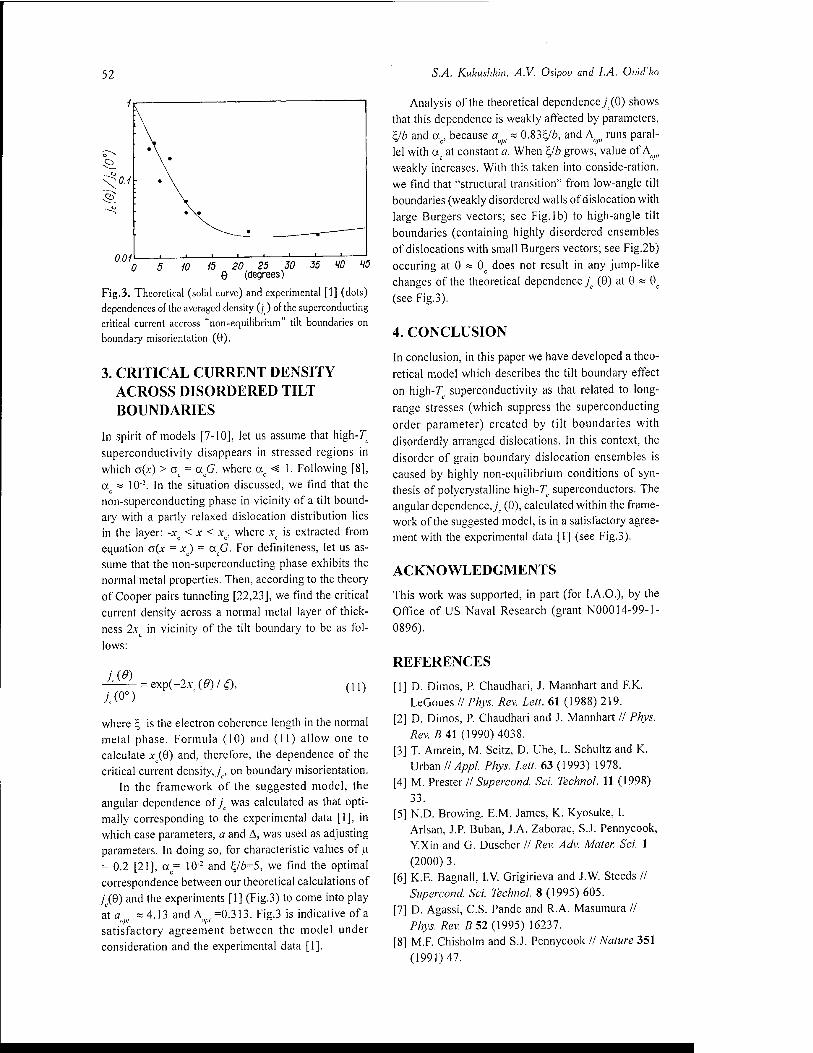
52 S.A. Kukushkin, A.V. Osipov and I.A. Ovid'ko
°'°*0 5 10 15 20 25 30 35 10 15 Q (degrees)
Fig.3. Theoretical (solid curve) and experimental [1] (dots) dependences of the averaged density (/ ) of the superconducting
critical current accross "non-equilibrium" tilt boundaries on
boundary misoricntation (9).
3. CRITICAL CURRENT DENSITY ACROSS DISORDERED TILT BOUNDARIES
In spirit of models [7-10], let us assume that high-T superconductivity disappears in stressed regions in which a(x) > a. = o.G, where ac « 1. Following [8], a ~ 10'2. In the situation discussed, we find that the
c
non-superconducting phase in vicinity of a tilt bound- ary with a partly relaxed dislocation distribution lies in the layer: -x < x < x, where xz is extracted from equation a(x = x) = aG. For definiteness, let us as- sume that the non-superconducting phase exhibits the normal metal properties. Then, according to the theory of Cooper pairs tunneling [22,23], we find the critical current density across a normal metal layer of thick- ness 2x in vicinity of the tilt boundary to be as fol-
lows:
1(0) exp(-2x (6>) / £), (11)
where £ is the electron coherence length in the normal metal phase. Formula (10) and (11) allow one to calculate xc(8) and, therefore, the dependence of the critical current density,^., on boundary misorientation.
In the framework of the suggested model, the angular dependence ofjc, was calculated as that opti- mally corresponding to the experimental data [1], in which case parameters, a and A, was used as adjusting parameters. In doing so, for characteristic values of u = 0.2 [21], ac= 10"2 and £Jb=5, we find the optimal correspondence between our theoretical calculations of y',(8) and the experiments [1] (Fig.3) to come into play at a ~ 4.13 and A =0.313. Fig.3 is indicative of a
opt <>l>l °
satisfactory agreement between the model under consideration and the experimental data [1].
Analysis of the theoretical dependence jc(Q) shows that this dependence is weakly affected by parameters, ZJb and occ, because a ~ 0.83^/6, and Ao/)/ runs paral- lel with ac at constant a. When £Jb grows, value of A weakly increases. With this taken into conside-ration, we find that "structural transition" from low-angle tilt boundaries (weakly disordered walls of dislocation with large Burgers vectors; see Fig.lb) to high-angle tilt boundaries (containing highly disordered ensembles of dislocations with small Burgers vectors; see Fig.2b) occuring at 8 « 9 does not result in any jump-like changes of the theoretical dependence^. (9) at 8 « 9c
(see Fig.3).
4. CONCLUSION
In conclusion, in this paper we have developed a theo- retical model which describes the tilt boundary effect
on high-71 superconductivity as that related to long-
range stresses (which suppress the superconducting
order parameter) created by tilt boundaries with disorderdly arranged dislocations. In this context, the
disorder of grain boundary dislocation ensembles is caused by highly non-equilibrium conditions of syn- thesis of polycrystalline high-T superconductors. The angular dependence,^ (8), calculated within the frame- work of the suggested model, is in a satisfactory agree- ment with the experimental data [1] (see Fig.3).
ACKNOWLEDGMENTS
This work was supported, in part (for I.A.O.), by the Office of US Naval Research (grant N00014-99-1-
0896).
REFERENCES
[1] D. Dimos, P. Chaudhari, J. Mannhart and F.K. LeGoues // Phys. Rev. Lett. 61 (1988) 219.
[2] D. Dimos, P. Chaudhari and J. Mannhart // Phys.
Rev. 5 41 (1990)4038. [3] T. Amrein, M. Seitz, D. Uhe, L. Schultz and K.
Urban II Appl. Phys. Lett. 63 (1993) 1978. [4] M. Prester // Supercond. Sei. Technol. 11 (1998)
33. [5] N.D. Browing, E.M. James, K. Kyosuke, I.
Arlsan, J.P. Buban, J.A. Zaborac, S.J. Pennycook, Y.Xin and G. Duscher // Rev. Adv. Mater. Sei. 1
(2000) 3. [6] K.E. Bagnall, I.V. Grigirieva and J.W. Steeds //
Supercond. Sei. Technol. 8 (1995) 605. [7] D. Agassi, C.S. Pande and R.A. Masumura //
Phys. Rev. 5 52(1995) 16237. [8] M.F Chisholm and S.J. Pennycook // Nature 351
(1991)47.

Critical Current Density in Polycrystalline High-T Superconductors with Disordered Tilt Boundaries 53
[9] K. Jagannadham and J. Narayan // Philos. Mag.
61 (1990) 129. [10] A. Gurevich and E.A. Pashitskii // Phys. Rev. B
57(1998) 13878. [11] H. Hilgenkamp, J. Mannhart and B. Mayer //
Phys. Rev. 5 53(1996) 14586. [12] S.E. Babcock and D.C. Larbalestier II Appl.
Phys. Lett. 55(1989)393. [13] D.M. Kroeger, A. Choudhary, J. Brynestad,
R.K. Williams, R.A. Padgett and W. Goghlan //
J.Appl. Phys. 64(1988)331. [14] A.Yu. Kraevskii and I.A. Ovid'ko // Phys. Sol.
State 42 (2000). [15] A.A. Nazarov, A.E. Romanov and B. Baudelet //
Philos. Mag. Lett. 68 (1993) 303. [16] A.A. Nazarov, R.Z. Valiev and A.E. Romanov //
Sol. State Phen. 35/36 (1994) 381.
[17] J.P. Hirth and J. Lothe, Theory of Dislocations
(N.Y.:McGraw-Hill, 1975). [18] A.P. Sutton and R.W. Balluffi, Interfaces in
Crystalline Materials (Oxford, Clarendon Press,
1995). [19] K.N. Mikaelyan, I.A. Ovid'ko and A.E. Romanov
// Mater. Sei. Eng. A 259 (1999) 132. [20] I.A. Ovid'ko // Mater. Sei. Eng. A 280 (2000)
355. [21] M. Cankurtaran, G.A. Saunders, J.R. Willis, A.
Al-Kheffaji and D.P. Almond // Phys. Rev. B 39 (1989)2872.
[22] P.G. De Gennes // Rev. Mod. Phys. 36 (1964)
225. [23] A. Barone and G. Paterno, Physics and Applica-
tions of the Josephson Effect (N.Y., Wiley,
1982).

Mater.Phys.Mech.l (2000)54-59
TEM AND STM INVESTIGATIONS ON THE DISCLINATION NATURE OF FRAGMENT BOUNDARY TRIPLE JUNCTIONS
M. Seefeldt
Freiberg University of Mining and Technology, Institute of Physical Metallurgy, Gustav-Zeuner-Straßc 5, D-09596 Freiberg, Germany
Present address: Catholic University of Leuvcn, Department of Metallurgy and Materials Engineering, Willem de Croylaan 2, B-3001 Heverlee, Belgium
Received: October 30, 1999
Abstract. After a short review of recent TEM measurements to characterize partial disclinations in fragment boundary triple junctions in cold-rolled copper, STM results from the same specimens are presented which support a disclination interpretation of the observed fragment structure. The role of the fragment boundary mosaic or of the corresponding immobile partial disclination network in work-hardening is discussed. Although the oricntational mismatches around the fragment boundary triple junctions are only small, the disclination contribution dominates work-hardening behaviour at large strains.
1. INTRODUCTION
The substructure development of crystalline metals under cold deformation up to large strains is characterized by the formation of a fragment structure on the mesoscopic scale [1]. Typically, with increasing strain the mean fragment size decreases monotonously starting from the micrometer range, whereas the mean misorientation across the fragment boundaries in- creases monotonously reaching several degrees [1-3]'. In contrast to the cell structure, the fragment structure does not saturate2 and its formation and evolution are quite universal phenomena which are observed in fee, hdp, and bec single- as well as polycrystals [1].
While the coexistence of the cell and fragment struc- tures and the evolutions of their characteristic param- eters are well investigated [1-3], the defect composition of the fragment boundary mosaic and its influence on work-hardening are not yet completely understood. Especially, to the authors' knowledge, there is no work- hardening model up to now which takes the fragment structure explicitly into account.
Following the Russian school of plasticity, the au- thors propose the triple junctions of the fragment
1 Hansen and coworkers use the term «cell block» instead of fragment. 2 Saturation means in this context that average cell structure parameters like cell size, cell wall width, or misorientation do not change any more.
Corresponding author: M. Seefeldt, e-mail: [email protected]
boundaries to have a disclination character [4-6] and, thus, to be sources of long-range stresses hindering dislocation motion and, thereby, contributing to work- hardening at large strains.
2. NONCOMPENSATED NODES OF FRAGMENT BOUNDARIES
According to experimental observations, a model de- scribing the fragment structure development as well as its coupling to the macroscopic mechanical behaviour requires tools which take into account such collective behaviour of dislocations that results into the formation, spread-out and enlargement of misorientations and into the presence of long-range stresses in the fragment interiors. A model on the sub- structure development and work-hardening under cold deformation up to large strains suggested by the present authors [7,8] uses disclinations [9,10] as such a tool. Especially, the formation of partial disclination dipoles (PDD) is modelled through incidental non-balanced trapping of neighbouring mobile dislocations of the same Burgers vector into cell walls and by incidental trapping of mobile dislocations with "matching" Burgers vector into preexisting fragment boundaries [8]. The first PDD configuration corresponds to a both- side terminated excess dislocation wall, the second one to a tilt or twist boundary segment with enlarged misorientation. To describe the non-conservative propa-
2000 Advanced Study Center Co. Ltd.

TEM and STM Inveslieatk the Disclinalion Nature of Fragment Boundary Triple Junctions 55
Fig. 1. A propagating partial disclination approaches a preexisting fragment boundary, is locked in this boundary and leaves an
orientational mismatch behind.
gation of the partial disclinations of such dipoles along cell walls or fragment boundaries, respectively, the capturing mechanism proposed by Vladimirov and Romanov [10,11] is used.
If a partial disclination propagates like that and approaches a preexisting fragment boundary, then it will rotate the crystal regions to the left and to the right of the growing backward fragment boundary against each other (Fig. lb). When it is finally locked in the preexisting fragment boundary, an orientational mismatch is left behind (Fig. lc). This mismatch can be accomodated in two different ways: either "plasti- cally" by generation of an additional dislocation bound- ary or "elastically" by rotational distortion. In the latter case, the triple junction is a non-compensated node containing a line defect of the disclination type.
3. TEM RESULTS
Since partial disclinations locked in the triple junc- tions of the fragment boundaries should - at least at low homologous temperatures - be stable under load relaxation, they are suitable objects for an experimen- tal confirmation of the disclination approach used in the above mentioned model. TEM microdiffraction measurements around fragment boundary triple junc- tions in copper single and polycrystals rolled down to 70% and 50% thickness reduction at room tempera- ture, respectively, showed [12] - that the product of the three misorientation matri-
ces does not give the identity and - that the local orientation varies continuously when
passing with the electron beam by the node. Whereas the first observation proves an orientational mismatch, the second one points towards its accomodation by elastic distortion rather than by an additional dislocation boundary. Both items together indicate that the triple junction includes an additional line defect which has - probably beside other
contributions [13,14] - a disclination nature. The measured orientational mismatches correspond to Frank vectors of
&> = [-0.0292,0.0094,0.0052] with\a>\= 1.78°, (1)
for a node in the single crystal specimen and
co = [-0.0046,-0.0316,0.0004] with [SJ|= 1.93°, (2)
for a node in the polycrystal specimen. These PD pow- ers are in good agreement with the theoretical expec- tation of |<»|«l-3° given by Romanov and Vladimirov in [10]. At present, PDD groups in a copper single crystal rolled down to 60% thickness reduction as shown in the TEM micrographs in Figs. 2 and 3 are analysed.
First results indicate that the PDD groups are not fully compensating dipole (Fig. 2) and quadrupole (Fig. 3) configurations, respectively [15].
4. STM RESULTS
Since it is very difficult to find sufficiently large per- fect crystal volumes to obtain Kikuchi patterns in the surroundings of the nodes in heavily deformed metals, an additional local characterization method which does not make use of diffraction is desirable. Scanning tun- nel microscopy (STM) is such a method. In their pio- neering works, Vettegren' et al. [16-20] have studied the profiles of polished surfaces of loaded copper, gold, and molybdenum specimens and found clusters of etch pits. The pits have been explained by the exit of dislo- cation groups after bursting through barriers on inter- secting glide planes, whereas the clusters have been interpreted as an early stage of crack formation [21].
Unfortunately, the STM contrast theory is not yet very well developed. It is known [22] that the strong electric field between the tip and the surface has an etching effect. It is generally admitted that this "field etching" should also result into preferred evaporation

56 M. Seefeldl
Fig. 2. TEM micrograph of a partial disclination dipolc
configuration. Copper single crystal rolled down to 60%
thickness reduction at room temperature. 2.61x1.90 u.nr.
and/or surface diffusion at high-energy surface regions.
From an analogy to Mullins' thermal etching theory
[23], one can conclude that etch grooves should arise
and deepen at the lines where planar defects like grain boundaries or fragment boundaries reach the surface. Depth and shape z(x,l) of the grooves scale with the plane energy y of the planar defect, e.g. for thermal etching with dominating evaporation and condensation
through [23]
z(x,t) = -2tan/?V/f/ ierfc 2^ At
(3)
with ß defined by the mechanical equilibrium between the planar defect (e.g. grain boundary) tension and the surface tensions, 2yy/sinß =y and A given by
A = pur«n
(2xMyn(kJ)2 (4)
with vapour pressure p0 for plain surface, atomic vol- ume Q. atomic mass M and temperature T. Fragment boundaries can be approximated as low-angle grain boundaries, so that their plane energy can be expressed through the misorientation, e.g. for a tilt boundary [24]
Gb r, 4^(1 - v)
f b A
In —- - In <p
I ';, ) (5)
with misorientation q> and dislocation core radius r0. Thus, at least in the thermal etching analogy, the groove depth and shape are directly related to the fragment boundary misorientation. Correspondingly, "field etch- ing" should also result into notching of etch pits at the points where line defects like dislocations or disci inations reach the surface. Depth and shape of the pits should then scale with the line energy, that means
Fig. 3. TEM micrograph of a partial disclination quadrupolc
configuration. Copper single crystal rolled down to 60%
thickness reduction at room temperature. 1.59x1.16 U,m .
with the powers or with the moduli of the Burgers or
Frank vectors, respectively. Although Romanov has
given the elastic fields around PDDs reaching the sur-
face [25], there is no etch pit theory up to now, not even for the thermal analogy. Therefore, the following discussion has to remain a qualitative one: If the triple junctions of fragment boundaries include additional high-energy line defects, then the corresponding etch pits should be much deeper than the etch grooves corresponding to the joining fragment boundaries.
For the present work, cut surfaces of copper poly- crystals rolled at room temperature have been abraded, polished and treated with the basic alumina OPS be-
Fig. 4. STM surface profile with fragment boundary grooves. Copper polycrystal rolled down to 70% thickness reduction at
room temperature. Arrow "A" marks a splitting point of a
fragment boundary, arrow "B" a triple junction, arrows "C" a
chain of nearly equidistant shallow etch pits. 5x5 U.m2. Grey scale from white to black corresponding to 15 nm depth.
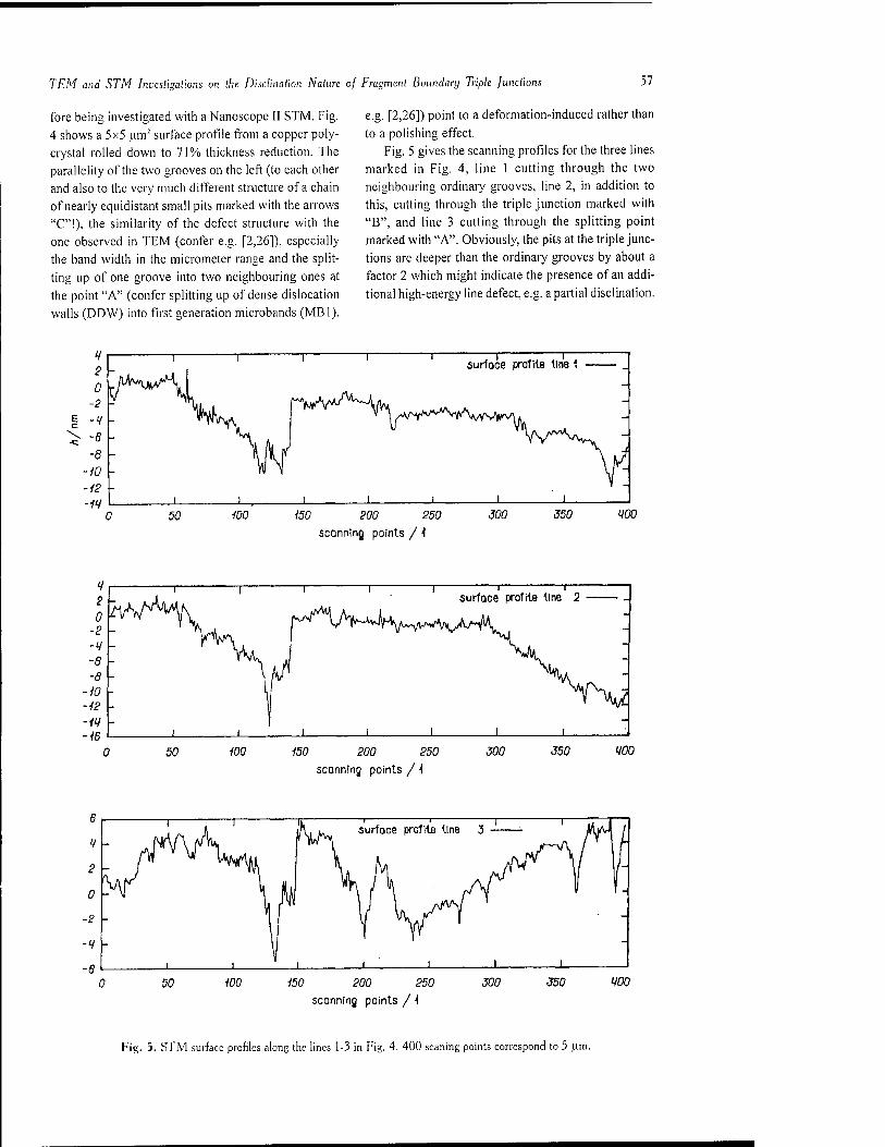
TEM and STM Investigations on the Disclination Nature of Fragment Boundary Triple Junctions 57
fore being investigated with a Nanoscope II STM. Fig. 4 shows a 5x5 urn2 surface profile from a copper poly- crystal rolled down to 71% thickness reduction. The parallelity of the two grooves on the left (to each other and also to the very much different structure of a chain of nearly equidistant small pits marked with the arrows "C"!), the similarity of the defect structure with the one observed in TEM (confer e.g. [2,26]), especially the band width in the micrometer range and the split- ting up of one groove into two neighbouring ones at
the point "A" (confer splitting up of dense dislocation walls (DDW) into first generation microbands (MB1),
e.g. [2,26]) point to a deformation-induced rather than
to a polishing effect. Fig. 5 gives the scanning profiles for the three lines
marked in Fig. 4, line 1 cutting through the two neighbouring ordinary grooves, line 2, in addition to this, cutting through the triple junction marked with "B", and line 3 cutting through the splitting point marked with "A". Obviously, the pits at the triple junc- tions are deeper than the ordinary grooves by about a factor 2 which might indicate the presence of an addi-
tional high-energy line defect, e.g. a partial disclination.
50 100 150 200 250 sconnlng points / i
300 350 WO
50 WO 150 200 250 sconnlng points / i
300 350
50 150 200 250 sconning points / \
350 WO
Fig. 5. STM surface profiles along the lines 1-3 in Fig. 4. 400 scaning points correspond to 5 p.m.
58 M. Seefeldi
5. EFFECT ON WORK-HARDENING
In a disclination-based model for the fragment struc- ture development like the one proposed in [7,8], propa- gating PDDs are immobilized as discussed in section 2 and Fig. 1 - resulting in a mosaic of fragment bound- aries or, correspondingly, in a network of immobile partial disclinations in the node lines of this mosaic. The evolutions of the cell wall dislocation density and
of the propagating and immobile disclination densi-
ties can be described with the equations [8]
de
dO
de
lJpr-Rpe,
N
Kr
TV v O.-J 6 0
de - = JJ6 0
de
(6)
(7)
(8)
including immobilization (/-term) of mobile and dy- namic recovery (/?-term) of mobile with cell wall dis- locations, PDD generation by incidental non-balanced trapping of N neighbouring mobile dislocations into cell walls (/f-term) and by incidental trapping of mo- bile dislocations with the "right" Burgers vector into fragment boundaries (K-term), and immobilization of propagating PDDs in the network of immobile ones (./-term). The coefficients can be estimated from physi- cal models for the elementary processes [7,8]. Whereas the cell wall dislocation density saturates according to the Kocks-type equation (6), the immobile disclination density increases monotonously according to equation (8) - corresponding to a monotonously decreasing mean fragment size.
The cell wall dislocation density is coupled to a flow stress contribution according to
A<x = (9)
where m is the Schmid factor and E, denotes the vol- ume fraction of the cell walls. The effect of the immo- bile disclination density on the flow stress is described by Romanov's and Vladimirov's law [10]
k<70=ßG\a\ (10)
The mean disclination power |cb| is equivalent to the average orientational mismatch around the node lines and may - following the discussion in section 2 and Fig. 1 - be approximated by the mean misorientation cp. Assuming a Poisson-Voronoi geometry of the frag- ment boundary mosaic, the mean misorientation is
calculated by distributing the available excess disloca- tion density which develops according to (£-term de- scribes capturing of mobile dislocations by propagat- ing partial disclinations)
^=Ktjr+K,Jei+E0i, (11) de
on the total fragment boundary plane area, finally giv-
ing [7]
<p«bpm/l.2U (12)
Integration of the evolution equations (6-8) and the flow stress contributions (9-10) shows that the disclination contribution to flow stress dominates the dislocation one starting from a von Mises strain of about 0.9 (parameters for copper at room temperature). Stage
III of single crystal plastic deformation can be attrib- uted to cell structure or dislocation work-hardening,
stage IV to fragment or disclination work-hardening
[7,8].
6. CONCLUSIONS
TEM microdiffraction measurements indicate the pres- ence of line defects of disclination nature in the triple junctions of fragment boundaries. STM shows deep etch pits at the points where the triple junction lines reach the surface — pointing to high-energy line defects in the triple junctions. Although the orientational mismatches remain small, the disclination long-range stress fields do have a significant influence on work- hardening and even dominate the dislocation contribution at large strains.
REFERENCES
[1] V.V. Rybin, Large Plastic Deformation and the Fracture of Metals (Metallurgiya, Moskva, 1986) (in Russian).
[2] B. Bay, N. Hansen, D.A. Hughes and D. Kuhlmann-Wilsdorf // Ada Metall. Mater. 40 (1992)205.
[3] Q. Liu, D. Juul Jensen and N. Hansen // Ada Mater. 46(1998)5819.
[4] V.A. Likhachev and V.V. Rybin // Izv. Akad. Nauk. SSSR Fiz. 37 (1973) 2433.
[5] V.l. Vladimirov and I.M. Zhukovskiy // Fiz. Tverd. 7e/a 16(1974)346.
[6] V.A. Likhachev and V.V. Rybin // Fiz. Tverd. Tela 18(1976) 163.
[7] M. Seefeldt and P. Klimanek // Modelling Simul. Mater. Sei. Eng. 6 (1998) 349.
[8] M. Seefeldt, V Klemm and P. Klimanek, in: Investigations and Applications of Severe Plastic
TEM and STM Investigations on the Disclination Nature of Fragment Boundary Triple Junctions 59
Deformation, Proceedings of the NATO Ad- vanced Research Workshop, edited by T.C. Lowe and R.Z. Valiev (Kluwer, Dordrecht, 1999), in
print. [9] R. de Wit // J. Res. Natl. Bur. Stand. (US) A 77
(1973)49, 359 and 607. [10] A.E. Romanov and V.l. Vladimirov, Disclinations
in Crystalline Solids, in: Disclinations in Solids,
vol. 9, edited by F.R.N. Nabarro (North Holland,
Amsterdam, 1992) p. 191.
[11] V.l. Vladimirov and A.E. Romanov // Fiz.
Tverd. Tela 20 (1978) 3114. [12] V Klemm, P. Klimanek and M. Seefeldt // Phys.
Stat. Sol. (a) 175 (1999) 569. [13] V.V. Rybin, N.Yu. Zolotorevskiy and I.M.
Zhukovskiy // Fiz. Met. Metalloved. 69 (1990) 5. [14] V.V. Rybin, A.A. Zisman and N.Yu. Zolotorevskiy
II Acta Metall. Mater. 41 (1993)2211. [15] V Klemm, P. Klimanek and M. Seefeldt, to be
published. [16] V.l. Vettegren', S.Sh. Rakhimov and V.N.
Svetlov // Fiz. Tverd. Tela 37 (1995) 913.
[17] V.l. Vettegren', S.Sh. Rakhimov and E.A. Bakulin // Fiz. Tverd. Tela 37 (1995) 3630.
[18] V.l. Vettegren', S.Sh. Rakhimov and V.N. Svetlov // Fiz. Tverd. Tela 37 (1995) 3635.
[19] V.l. Vettegren', S.Sh. Rakhimov and V.N. Svetlov // Fiz. Tverd. Tela 38 (1996) 590.
[20] V.l. Vettegren', S.Sh. Rakhimov and V.N. Svetlov // Fiz. Tverd. 7e/a38(1996) 1142.
[21] VI. Vettegren', V.L. Gilyarov, S.Sh. Rakhimov
and V.N. Svetlov // Fiz. Tverd. Tela 40 (1998)
668. [22] T.T. Tsong // Phys. Rev. B 44 (1991) 13703. [23] W.W. Mullins II J. Appl. Phys. 28 (1957) 333. [24] P. Paufler and G.E.R. Schulze, Physikalische
Grundlagen mechanischer Festkorperei- genschaften I (Akademie-Verlag, Berlin, 1978).
[25] A.E. Romanov // Poverkhnost' 6 (1982) 121. [26] D.A. Hughes and N. Hansen // Mater. Sei.
Technoi 7(1991)544.

A7
International Workshop on
INTERFACE CONTROLLED MATERIALS: RESEARCH AND DESIGN (ICMRD) Si.Petersburg, Russia, June 7-9, 2000
Announcement: Much of the recent advancement in technology is based on new and novel materials that have been designed for specific functions. The application of these materials is responsible for the growth of industrial sectors such as electronics, energy and aerospace engineering. The objective of this Workshop is to present current research on advanced interface controlled materials with primary focus on nanostructured materials and high transition- temperature superconducting materials (characterized by nano-scaled coherence length). Special attention will be paid to design of such interface controlled materials with their unique and highly desirable properties. The Workshop objectives are to assess the current status and to identify future directions of research, design and applications of nanostructured bulk solids, films and coatings as well as polycrystalline superconducting materials. Particular emphasis is placed on developing close interactions and fostering future collaborations among scientists and
engineers from Russia, the USA and other countries.
We plan to focus on the following topics: Synthesis and processing;
Modeling; Characterization and properties (mechanical and transport properties of nanostructured materials, high- and low-
current properties of superconducting polycrystalline materials);
Design; Applications.
International Organizing Committee:
I.A.Ovid'ko (Russian Academy of Sciences, Russia) B.I.Smirnov (Russian Academy of Sciences, Russia) C.S.Pande (Naval Research Laboratory, USA) M.Soto (Office of the US Naval Research, USA)
B.B.Rath (Naval Research Laboratory, USA)
Submission of Abstracts for Oral and Poster Presentations:
Anyone interested in making a contribution to the workshop is invited to submit by email a half page abstract with
an application form to Dr.Ilya Ovid'ko (E-mail: [email protected]) by MAY 1, 2000
Current info on the ICMRD meeting and the application form can be found on the web-site:
http://mclab.me.uic.edu/activities.htm
Invited Speakers: S.Babcock (University of Wisconsin at Madison, USA), U.Balachandran (Argonne National Laboratory, USA), M.Baro (UAB; Bellaterra, Spain), G.M.Chow (National University of Singapore, Singapore), Y.Gogotsi (University of Illinois at Chicago, USA), H.Hilgenkamp (University of Twente, The Netherlands), Y.Hwu (Institute of Phys- ics, Taiwan), P.Jena (Virginia Commonwealth University, USA), A.King (Purdue University, USA), G.Kiriakidis (IESL, Greece), P.Klimanek (Freiberg Technical University, Germany), M. Muhammed (Royal Institute of Tech- nology, Sweden), T.Ovid'ko (Russian Academy of Sciences, Russia), M.Seefeldt (K.University of Leuven, Bel- gium), B.Smirnov (Russian Academy of Sciences, Russia), C.Pande (Naval Research Laboratory, USA), S.Ranganathan (Indian Institute of Science, India), B.B.Rath (Naval Research Laboratory, USA), A.Romanov (Russian Academy of Sciences, Russia), R.E.I.Schiopp (Utrecht University, The Netherland), M.Soto (Office of Naval Research, USA), B.Starumal (Russian Academy of Science, Russia), T.Tsakalakos (Rutgers University, USA), T.Watanabe (Tohohku University, Japan), T.Yamasaki (Himeji Institute of Technology, Japan), A.Zhilyaev
(Ufa State Aviation University, Russia).
A8
ADVANCED STUDY CENTER. TRANSFER OF COPYRIGHT AGREEMENT
Article entitled:
Corresponding author:
To be published in the journal: "Materials Physics and Mechanics"
Effective upon acceptance for publication, copyright (including all rights thereunder and including the right to authorise photocopying and reproduction in all media, whether separately or as a part of a journal issue or other- wise) in the above article and any modifications of it by the author(s) is hereby transferred throughout the world and for the full term and all extensions and renewals, to: "Advanced Study Center" Co. Ltd., (Si. Petersburg, Russia)
This transfer includes the right to adapt the presentation of the article for use in conjunction with computer systems and programs, including reproduction or publication in machine-readable form and incorporation in retrieval systems.
Rights of authors
The following rights are retained by the author(s): 1. Patent and trademark rights and rights to any process or procedure described in the article. 2. The right to photocopy or make single electronic copies of the article for their own personal use, including for
their own classform use, or for the personal use of colleagues, provided the copies are not offered for sale and are not distributed in a systematic way outside of their employing institution (e.g. via an e-mail list or public file server). Posting of a preprint version of this work on an electronic public server is permitted. Posting of the published article on a secure network (not accessible to the public) within the author's institution is permitted. However, posting of the published article on an electronic public server can only be done with written permis- sion of Advanced Study Center. Co. Ltd.
3. The right, subsequent to publication, to use the article or any part thereof free of charge in a printed compilation of works of their own, such as collected writings or lecture notes, in a thesis, or to expand the article into book-length form for publication.
Note
All copies, paper or electronic, or other use of the information must include an indication offne copyright ownership and a full citation of the journal source. Please refer requests for all uses not included above, including the authori- zation of third parties to reproduce or otherwise use all or part of the article (including figures and tables) to:
Materials Physics and Mechanics Editorial Office
Institute of Problems of Mechanical Engineering Russian Academy of Sciences
Bolshoj 61, Vas.Ostrov, St.Petersburg 199178, Russia E-mail: [email protected]
Fax:+(7 812)321 4771
Authorship
If the article was prepared jointly with other author(s), the signing author has informed the co-author(s) of the terms of this copyright transfer and is signing on their behalf as their agent and represents that he or she is authorized to do so. Please confirm by marking the appropriate box following the signature line. The signing author shall bear the responsibility for designating the co-author(s) and must inform Advanced Study Center of any changes in authorship. If copyright is held by the employer, the employer or an authorized representative of the employer must sign. If the author signs, it is understood that this is with the authorization of the employer and the employer's acceptance of the terms of the transfer. Please confirm by marking the appropriate box following the signature line.
Warranties
The author(s) warrant(s) that the article is the author's original work and has not been published before. The aurthor(s) warrant(s) that the article contains no libelous or other unlawful statements, and does not infringe on
A9
the rights of others. If experts from copyrighted works are included, the author(s) has (have) obtained or wil obtain written permission from the copyright owners and will credit the sources in the article.
Signature of copyright owner(s) *:
Name (printed):
Title (if employer representative):
Company or institution:
Date:
If any of the following apply, please mark the box(es): D author on behalf of all co-authors D employer representative
PLEASE SIGN IN INK AND RETURN THE COMPLETE ORGIGINAL (do not send by fax), retaining a copy of this form for your files, TO:
Materials Physics and Mechanics Editorial Office
Institute of Problems of Mechanical Engineering Russian Academy of Sciences
Bolshoj 61, Vas.Ostrov, St.Petersburg 199178, Russia E-mail: mpm@def,ipme.ru
Fax:+(7 812)321 4771
*To be signed by the author, also on behalf of any co-authors, or to be signed by employer, where appropriate.
INSTRUCTIONS FOR AUTHORS
Submission of papers: Manuscript should be submitted in English in both electronic (by e-mail) and hard copy (original +copy) versions. Hard copy submission: Manuscripts should be submitted typed on good quality bond paper of A4 format with 1" margins (right, left, top, bottom), double-spaced, using Times Roman 12 pt font, to:
Materials Physics and Mechanics Editorial Office Institute of Problems of Mechanical Engineering Russian Academy of Sciences Bolshoj 61, Vas.Ostrov, StPetersburg, 199178, Russia Fax: -H7 812)321 4771
Electronic submission: Manuscripts should be submitted by e-mail to: E-mail: [email protected] Filetypes: TeX (LaTeX) and MS Word files preferred. LaTeX style files are available on the Web-site: http:// www.ipme.ru/e-journals/MPM/. Pictures and photos should be submitted in TIFF format (400 dpi).
Length: Papers should be limited to 30 typewritten pages (including Tables and Figures each on separate page).
Structure of the manuscript: Cover sheet; Text; Tables; References; Figure Captions; Pictures and Photos
A cover sheet should be included that contains the complete title, the names, affiliations, mailing addresses of the authors, fax and e-mail address of the corresponding author and the abstract. TITLE - bold, centered. (14 pt) Author(s) - bold, centered, e.g. S. R. Brown and T. Klein Affiliation(s) - centered, complete postal address for all authors, e-mail address of corresponding author.
ABSTRACT. About 150-200 words.
Tables: type each table on the separate page, number consecutively in arabic numerals and supply a heading.
References: References should be indicated in the text by consecutive numbers in square parentheses, e.g. [1,2,5-7], as a part of the text, the full reference being cited at the end of the text. References should contain the names of the authors together with their initials, the title of the journal, volume number, year and the first page number as illustrated below. References to books should contain the names of the authors, the title (the names of editors), the publisher name, location and year, as illustrated below.
REFERENCES [1] R. Birringer, H. Gleiter, H.P. Klein and P. Marquardt///%*. Lett. 102 (1984) 365. [2] F.R. Nabarro, Theoiy of Crystal Dislocations (Clarendon Press, Oxford, 1967). [3] V. Provenzano, In: NanostructuredMaterials: Science and Technology, ed. by G.-M. Chow and N.I Noskova
(Kluwer: Dordrecht, 1998), p. 335.
Figures: For best results submit illustrations in the actual size at which they should be published. The line drawings of the original should be laser printed, the photographs should be original, with somewhat more contrast than is required in the printed version. Each figure should be typed on separate page, the listing of the figure captions must be included.
Equations must be clearly printed and numbered sequentially with arabic numbers enclosed with round parentheses at the right-hand margin.
Units - the authors are encouraged to use the Si-units, other units are also acceptable.
OTnenaTaHo B Timorpa^HH «Amvr-Crfö»
rapmnypa Tamnc, no/uincaHO K neqara 06.04.2000
yen. ne*i. JI. 9.5, rapaac 950 3K3., 3aKa3 289.
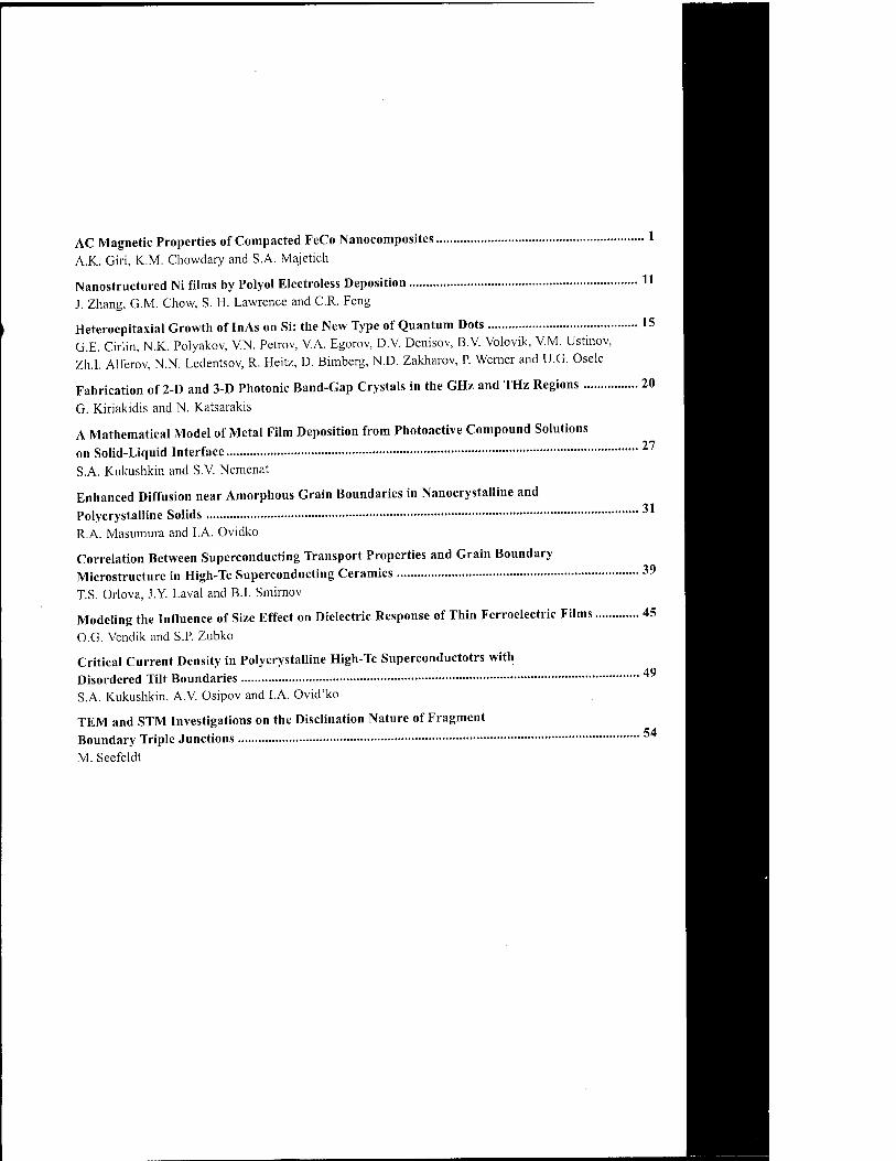
AC Magnetic Properties of Compacted FeCo Nanocomposites 1
A.K. Giri, K.M. Chowdary and S.A. Majetich
Nanostructured Ni films by Polyol Electroless Deposition U
J. Zhang, G.M. Chow, S. H. Lawrence and C.R. Feng
Heteroepitaxial Growth of InAs on Si: the New Type of Quantum Dots 15 G.E. Cirlin, N.K. Polyakov, V.N. Petrov, V.A. Egorov, D.V. Denisov, B.V. Volovik, V.M. Ustinov, Zh.l. Alferov, N.N. Ledentsov, R. Heitz, D. Bimberg, N.D. Zakharov, P. Werner and U.G. Osele
Fabrication of 2-D and 3-D Photonic Band-Gap Crystals in the GHz and THz Regions 20
G. Kiriakidis and N. Katsarakis
A Mathematical Model of Metal Film Deposition from Photoactive Compound Solutions 27 on Solid-Liquid Interface
S.A. Kukushkin and S.V. Nemenat
Enhanced Diffusion near Amorphous Grain Boundaries in Nanocrystalline and
Polycrystalline Solids R.A. Masumura and I.A. Ovidko
Correlation Between Superconducting Transport Properties and Grain Boundary Microstructure in High-Tc Superconducting Ceramics 39
T.S. Orlova, J.Y. Laval and B.I. Smirnov
Modeling the Influence of Size Effect on Dielectric Response of Thin Ferroelectric Films 45
O.G. Vendik and S.P. Zubko
Critical Current Density in Polycrystalline High-Tc Superconductotrs with 49 Disordered Tilt Boundaries • ^
S.A. Kukushkin, A.V. Osipov and I.A. Ovid'ko
TEM and STM Investigations on the Disclination Nature of Fragment S4 Boundary Triple Junctions Jn
M. Seefeldt