Materials and surface aspects in the development of SRF...
111
EuCARD-BOO-2012-001 European Coordination for Accelerator Research and Development PUBLICATION Materials and surface aspects in the development of SRF Niobium cavities Antoine, C (DSM IRFU CEA Centre d’Etudes de Saclay) 09 August 2012 The research leading to these results has received funding from the European Commission under the FP7 Research Infrastructures project EuCARD, grant agreement no. 227579. This work is part of EuCARD Work Package 10: SC RF technology for higher intensity proton accelerators and higher energy electron linacs. The electronic version of this EuCARD Publication is available via the EuCARD web site <http://cern.ch/eucard> or on the CERN Document Server at the following URL : <http://cdsweb.cern.ch/record/1472363 EuCARD-BOO-2012-001
Transcript of Materials and surface aspects in the development of SRF...

EuCARD-BOO-2012-001
European Coordination for Accelerator Research and Development
PUBLICATION
Materials and surface aspects in thedevelopment of SRF Niobium cavities
Antoine, C (DSM IRFU CEA Centre d’Etudes de Saclay)
09 August 2012
The research leading to these results has received funding from the European Commissionunder the FP7 Research Infrastructures project EuCARD, grant agreement no. 227579.
This work is part of EuCARD Work Package 10: SC RF technology for higher intensityproton accelerators and higher energy electron linacs.
The electronic version of this EuCARD Publication is available via the EuCARD web site<http://cern.ch/eucard> or on the CERN Document Server at the following URL :
<http://cdsweb.cern.ch/record/1472363
EuCARD-BOO-2012-001
Materials and surface aspects
in the development of SRF Niobium cavities
Claire Antoine

2
TABLE OF CONTENTS
Foreword from W. Singer ....................................................................................................................................... 5
Foreword from the author ........................................................................................................................................ 7
1. Introduction: the performances of superconducting RF cavities .................................................................... 9
1.1. Radiofrequency resonators: a brief summary ......................................................................................... 9
1.1.2 Comparing copper and Niobium: .................................................................................................... 10
1.1.3 Choice of the frequency ............................................................................................................... 11
1.1.4 The theoretical limitations of Niobium ........................................................................................... 11
Superheating field ...................................................................................................................................... 12
Vortex nucleation ...................................................................................................................................... 13
Surface resistance ...................................................................................................................................... 14
1.1.5 The practical limitations of Niobium cavities ................................................................................. 14
1.2. How to get a “good” cavity? (Summary) ............................................................................................. 16
1.2.1 Purity: high RRR material required ................................................................................................. 16
Residual Resistivity Ratio ......................................................................................................................... 16
Purity and thermal conductivity................................................................................................................. 18
Kapitza resistance ...................................................................................................................................... 20
Post purification ......................................................................................................................................... 20
1.2.2 Controlling the welds ...................................................................................................................... 20
1.2.3 A “good” surface state ..................................................................................................................... 21
1.2.4 Baking: highly efficient, but why? : ................................................................................................ 22
1.2.5 The A to Z of making of a cavity: ................................................................................................... 23
2. The metallurgy of high purity Niobium ........................................................................................................ 24
2.1. Introduction .......................................................................................................................................... 25
2.2. Mechanical behavior of high purity Niobium ...................................................................................... 25
2.2.2 Mechanical resistance of the cavities. ............................................................................................. 27
2.2.3 Mechanical properties and welding. ................................................................................................ 27
2.2.4 Grain size and mechanical properties .............................................................................................. 28
2.3. Cavity forming ..................................................................................................................................... 29
2.3.1 Manufacturing of cavities ................................................................................................................ 29
2.3.2 Formability ...................................................................................................................................... 29
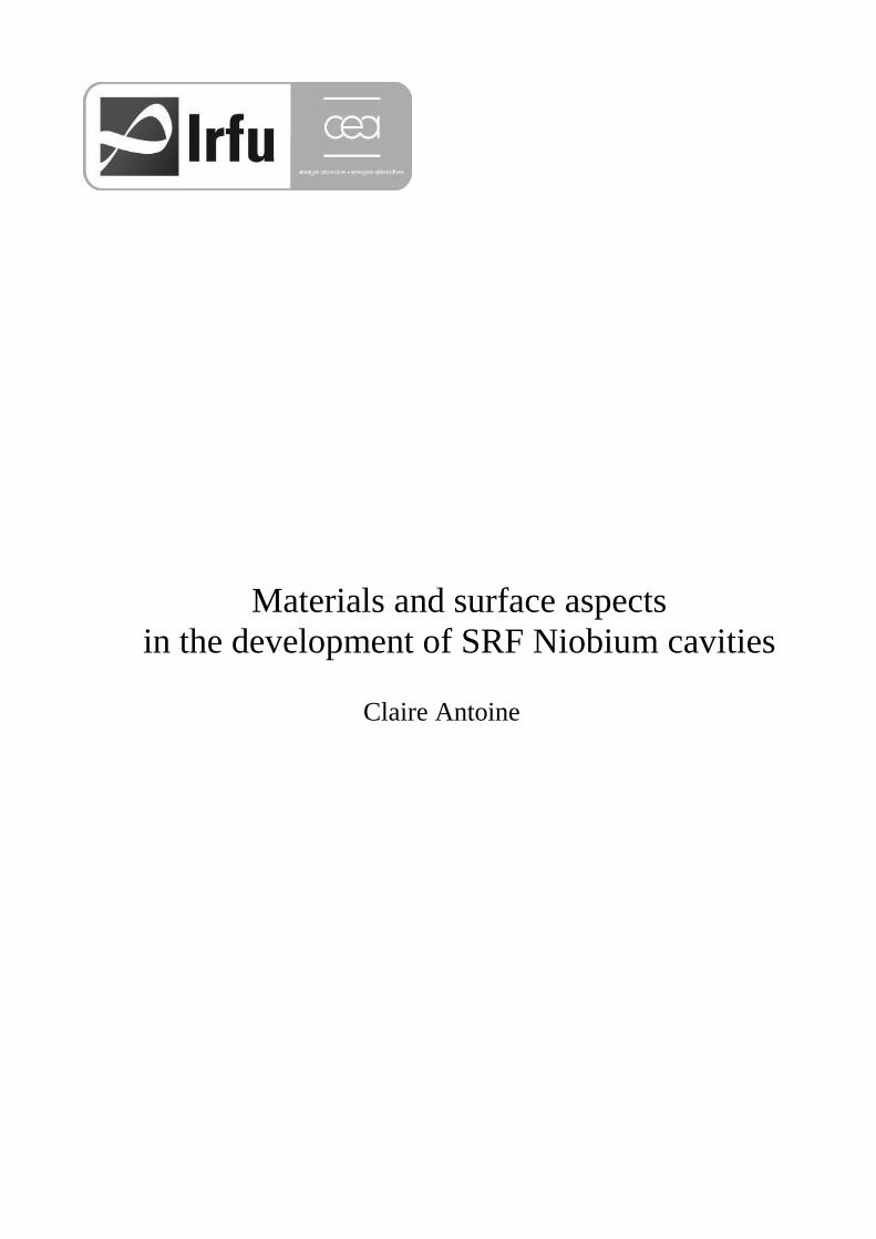
Stress-strain curves and formability .......................................................................................................... 30
Micrographs and tensile curves ................................................................................................................. 31
Strain hardening coefficient n .................................................................................................................... 31
2.3.3 Recrystallization and recovering in high purity Niobium ............................................................... 33
Recrystallization and actual furnace temperature: ..................................................................................... 34
2.3.4 Low temperature behavior ............................................................................................................... 35
2.4. Nb sheet production ............................................................................................................................. 37
2.4.1 Example of problems in industrial production ................................................................................ 37
2.4.2 « skin-pass », damaged layer and recrystallization ......................................................................... 37
2.4.3 Damaged layer and surface treatment. ............................................................................................ 39
Mechanical and mechanical-chemical polishing ....................................................................................... 39
New tumbling developments ..................................................................................................................... 40
2.4.4 Delivery controls and Quality insurance ......................................................................................... 40
2.4.5 Some comments about specifications .............................................................................................. 41
2.5. Large grain cavities: ............................................................................................................................. 42
2.5.1 Advantages of large grain materials ................................................................................................ 42
2.5.2 Drawbacks ....................................................................................................................................... 42
2.5.3 A technological exploit: monocrystalline cavities ........................................................................... 43
2.6. Damage, dislocations and superconductivity ....................................................................................... 44
3. Surface morphology and quench .................................................................................................................. 47
3.1. Surface morphology ............................................................................................................................. 47
3.2. Replicas at the quench site ................................................................................................................... 50
3.3. Modeling the generated field................................................................................................................ 52
3.4. Welding and roughness ........................................................................................................................ 54
4. Chemical contamination at the surfaces / interfaces of the Niobium ............................................................ 57
4.1. Surface composition and oxide-superconductor interface.................................................................... 57
4.2. Hydrogen .............................................................................................................................................. 58
4.2.2 The « 100K » effect or « Q-Disease » ............................................................................................. 58
4.2.3 Experimental observations .............................................................................................................. 59
4.2.4 Surface segregations and pure metals .............................................................................................. 61
4.3. Other surface contaminations ............................................................................................................... 61

3
4.3.2 Contaminations at the metal-oxide interface ................................................................................... 62
4.3.3 Oxidation of Niobium ..................................................................................................................... 64
4.3.4 Baking: hunting for interstitial oxygen ............................................................................................ 68
3D microprobe (Atom-Probe Tomography) .............................................................................................. 69
X ray diffraction (scattering diffusion, reflectometry and Crystal Troncation Rod) ................................. 70
4.4. Changes at the metal-oxide interface: towards new approaches. ......................................................... 71
4.4.2 Metal-superconductor interface and bound states. .......................................................................... 72
4.4.3 Tunneling Spectroscopy (point contact tunneling) .......................................................................... 72
4.5. Contamination at grain boundaries ...................................................................................................... 74
5. Outlook: breaking Niobium’s monopoly ...................................................................................................... 77
5.1. Criteria for choosing a « good » RF superconductor ........................................................................... 77
5.2. HC1, a hitherto neglected criterion. ....................................................................................................... 79
5.3. Superconducting nano-composites: an innovative path for the future of SRF ..................................... 79
6. Conclusion .................................................................................................................................................... 82
7. Appendices ................................................................................................................................................... 83
7.1. Appendix 1: Field Emission and Particulate Contamination ................................................................ 83
7.1.2 Influence of a particle’s morphology on its emissivity.................................................................... 84
7.1.3 Analysis of the steps in the process of surface preparation ............................................................. 85
7.1.4 Influence of assembly and vacuum handling .................................................................................. 85
7.1.5 « post processing », a future solution? ............................................................................................ 85
7.2. Appendix 2: Surface treatments. .......................................................................................................... 87
7.2.2 Electropolishing basics .................................................................................................................... 88
7.2.3 Aging of the EP solution, corrosion of the electrode and sulfur particles ....................................... 90
7.2.4 Field repartition, modeling .............................................................................................................. 90
7.2.5 Changing the composition ............................................................................................................... 91
7.3. Appendix 3: Nb machining/Forming ................................................................................................... 93
7.3.2 Forming ........................................................................................................................................... 93
7.3.3 Machining: ...................................................................................................................................... 93
7.3.4 Lubricant: discussion ....................................................................................................................... 93
7.3.5 Recommendations ........................................................................................................................... 93
7.4. Appendix 4 : Hydroforming ................................................................................................................. 95
7.4.2 Manufacture of the tubes ................................................................................................................. 95
7.4.3 Modeling ......................................................................................................................................... 96
8. Glossary and acronyms ................................................................................................................................. 99
9. Références .................................................................................................................................................. 103
Preamble:
Acronyms and some technical terms relating to cavities that are not directly related to the main topic are
explained in the glossary at the end of the book (they appear in italic bold in the text)

4
Figure 1 : Some examples of superconducting elliptical cavities

5
Foreword from W. Singer
In last two decades the SRF community reached immense progress in technology of fabrication and preparation
of superconducting resonators. For example beginning of nineties the required accelerating gradient of 15 MV.m-1
for
1.3 GHz 9-cell cavities for Tesla Test Facility was considered as an ambitious aim. Nowadays gradients of 45 MV.m-1
are demonstrated on such type of cavities. All this achievements have been reached thanks to improvements in our
understanding of many technological and fundamental aspects: e.g. procedures of material production from ore to
Niobium semi-finished product, material diagnostic, cavity fabrication procedure in particular the features of the
electron beam welding, preparation procedures in particular of the surface contamination and cleanness items etc. New
techniques and procedures have been developed and many of them applied in the meantime for cavity serial production,
for example for European XFEL: eddy current scanning, surface treatment by electropolishing, ethanol rinsing, baking
at 120°C. Good progress is achieved in fabrication of large grain cavities, weld-less fabrication by hydroforming or
spinning, dry ice cleaning etc. The most of mentioned aspects of innovative techniques are described and analyzed in
the book presented to the readers.
Significant progress in reaching high accelerating gradients stressed on the other hand the point, that we are
approaching to the performance limit of Niobium that is restricted by its critical magnetic field. Search for new
materials and new techniques for superconducting cavities become inevitable. In this context it was favorable to realize
that a lot of attention in the book is dedicated to the topic “what will break the Niobium’s monopoly”. The effort of the
last years is especially attracted to the multilayer coating, that possible could allow screening the magnetic field and
reach much higher accelerating gradients.
Creation of a SRF dedicated book after two fundamental monographs that appeared under leadership of Hasan
Padamsee (published 2008 and 2009) is not a grateful task. Such book has either to contain new data, or represent new
ideas, or at least introduce some issues deeper and more exhaustive. I would say that the work of author is succeeded in
this relation. The scope of the book is much narrower as by Padamsee and his coauthors, but complementary and
autonomous. A lot of new data, new aspects and interpretations in SRF material science can be found in it.
I know Claire Antoine as a thorough scientist that tries to understand issues up to smallest aspects and is steadily
on the search for new experiments or methods allowing finding out details of the phenomena. Among others she is the
scientist that is systematically extend her knowledge by reading the appropriate literature that helps inventing her new
concepts. It is not a surprise for me that after more as 20 years of scientific work she has a demand to summarize the
experiences and hand it over to younger generation and colleagues interested in the basics of the material for SRF
cavities.
The accelerator physicists often obligated to go deeper in details of material and surface science. The work of
Claire Antoine can in many aspects be very helpful from this point of view and definitely will be supporting for
newcomers in the accelerator technology and students. Author refers and describes in the text, by glossary and
acronyms many not conventional methods of the material surface analysis (e.g. ERDA, EBSD, GDS, ARXPS, PIXE,
Atom-Probe-Tomography, etc.). Such information can be appropriate even for experts in surface science and chemistry.
The book is written by open, not classical more colloquial style, but I do not think that it is a weakness. This
fresh style impresses and at the same time makes the readings not borrow.
Some thesis and conclusions are disputable as well as some interpretations are still on debates. From my point of
view such depiction is appropriate and will trigger the updated discussions in our community.

6
I personally had a fun reading the book and assume that future readers will get similar impression. I am pretty
sure that the work of Claire Antoine will excite interest in the SRF community.
Hamburg
11.05.2012
Dr. Waldemar Singer
Deutsches Elektronen-Synchrotron DESY

7
Foreword from the author
When I joined the CEA Saclay SRF group in 1989, my initial background was physical chemistry and surface
science, which I completed later on with solid state physics and metallurgy. Most accelerator physicists at that time had
training in RF, plasma physics, nuclear or particle physics. We were very few with a background in material science.
Working with people with a different background than yours reveals to be both challenging and funny: you can impress
them with things you consider basic while they simply do not believe you for other things you consider so well admitted
that you do not even remember where it comes from. At the end it obliges you to reconsider your basics and re-question
many results, which opens many new and sometimes unexpected paths. Like usual in science, answering one question
rises many new ones, and trying to improve cavities performance led to fascinating physics problems.
Exploring some of these problems often requires techniques and expertise that are far beyond the reach of one
sole SRF lab, even well-funded. I have always worked in collaboration with laboratories with established expertise. It is
a way of working I consider to be the only way to access new techniques. Indeed many today’s techniques, even
complex ones, can deliver experimental results by merely “pushing a button”. Correct interpretation of the results
requires advanced knowledge of the physics underneath as well as knowing the apparatus limitations or possible
artifacts. Collaboration with experienced scientists is the only way to protect oneself against fallacious interpretation.
The body of this monograph is based on my “habilitation” (HDR) thesis held in 2009 to join the University
Paris-Sud faculty. The initial text was mostly based on my personal work, but since I had touched nearly all material
and surface aspects in SRF over the past 22 years, I had also an introduction chapter on each topic with a lot of
references to others’ work. In the present text I have tried to develop this introductory part and support my descriptions
with more external references. A difficult task since lately the domain has been evolving very quickly and plenty of new
interesting results are published every month. At some point I had to accept that whatever I could write, it will only be a
partial picture of the SRF activity in the world at some date (let’s say 2011).
This text is destined to accelerator physicists who are not familiar with material and surface science and students
who enter the field. Its level is introductory, but I have also tried to develop prospective views, generally at the end of
each chapter. For this I benefited a lot from continuous exchange with physicists all around the world. I want to thank
here W. and X. Singer from DESY, G. Ciovati and J. Mammosser from JLab, A. Gurevich now at ODU, A.
Romanenko, now at FNAL or T. Proslier at ANL and many others… It is a pleasure to see that a whole new generation
of physicist is now trained in surface science, solid state physics or superconductivity theory, and that technical
developments for SRF cavities led to new physics exploration that in turn allowed pushing the cavities limits.
Some of the interpretations I put forward here are still debated. I deliberately decided to present things as I see
them, through my own personal “material scientist” prism. In science, I do not think there is such thing as being wrong
or right; we are simply describing the same thing with a different lighting. I hope that the lighting presented here will
help the reader to reach a new understanding of SRF materials.
I also wish to thank the reviewers to have helped me to improve this manuscript, which, I am sure, suffers a lot
from the fact that English is not my native language. I apologize in advance if some of my sentences sound a little
weird…
Saclay
30.01.2012
Dr. Claire Antoine

8

9
1. Introduction: the performances of superconducting RF cavities
This chapter describes briefly the whereabouts of RF cavities and the advantages of using superconducting
materials. More detail about RF aspects can be found in [1]. Note that the results presented in this monograph originate
mainly from the studies conducted on high gradient elliptical cavities, so called “TESLA shape”[2], but most of the
information on material properties is directly applicable for other types of cavities. We have restricted ourselves to
focus on the material and tried to correlate, when possible, with superconducting properties. The reader must keep
aware that some of the figures of merit on superconducting properties evoked below might change when dealing with
different range of energy and frequency.
1.1. Radiofrequency resonators: a brief summary
Radio frequency cavities are resonators that can store an electric field used for the acceleration of a bunch of
charged particles in an accelerator. There are several possible resonance modes, but in general only one of those (the
fundamental mode) will be suitable for acceleration (see Figure 2). The power is injected through a main coupler, but
other couplers -called « HOM » (High Order Mode) - are needed to remove the most disturbing harmonics. It is
necessary to use simulation by finite elements to calculate how the field distributes over the different structures under
consideration, in order to select the most suitable one. The cavities therefore are designed in such a way that the
generated electric field is directed along the beam axis. One injects the electrons (/protons/ions) in bunches, only during
the period when the field is in the proper direction for acceleration.
Figure 2. Diagram of the distribution of the electric field in a resonant cavity.
The cavities have been developed since the building of accelerators with energies of over ~100 MeV, when it is
no longer possible to obtain high electric fields by electrostatic means. Originally these cavities were made of copper, a
metal that has good electrical and thermal properties. Due to the Joule effect, though, it is not possible to get high
electric fields unless small duty cycle (pulsed beam). This has important consequences for the integrated intensity of the
beam.
The introduction of a superconducting material as replacement for the copper was an important innovation that
was proposed in the end of the 60‘s [3]. Its advantages will be described in more details in the following sections. There

10
are several superconductors that may be considered. It is Niobium, though (the pure metal with the highest transition
temperature TC and the highest transition magnetic field HC11) that gives the best results.
The performance of superconducting cavities is characterized by two parameters (Figure 3):
Figure 3 : Schematic performance of RF Niobium cavities
- The accelerating field Eacc, as seen by a particle traversing the cavity (sometimes called « gradient »).
- The overvoltage coefficient, or quality factor Q0, which measures the ability to store the electromagnetic
energy (Q0 is proportional to the ratio of the stored energy divided by the energy lost by dissipation).
Note that RF dissipation in a superconductor is not zero. We will come back to this point in more detail further
on in the text.
1.1.2 Comparing copper and Niobium:
Conventional cavities (made of copper) and superconducting cavities work according to the same principle. The
thermal dissipation and the conditions under which they function, are, however, very different. In the frequency range
that is used for « normal» accelerators, between 200-2000 MHz, we can roughly summarize the situation as in the
following table:
1 For type II superconductors like niobium, HC1 corresponds to the transition of the purely superconducting state to a mixed
state, where both superconducting and normal conducting areas are present, whereas HC2 corresponds to the transition of the mixed
state to the normal state. HC is the critical thermodynamic field. More details will be found in §1.1.4.

11
Table 1: Comparison copper-Niobium
Superconductor : Niobium Normal conductor : copper
- a better yield: the overvoltage coefficient is between 10
000 and 100 000 times bigger than for copper; less
thermal dissipation on surfaces, almost all the power of
the klystron transfers to the beam.
- dissipation because of Joule effect: to avoid melting of
the structures it is necessary to keep the average injected
power low ; most of it will be lost through heating of the
cavities.
- need to cool down to 2 K (-271 °C); the amount of
electricity needed to deliver the necessary cryogenic
power considerably lowers the - in principle - much
higher efficiency.
- long duty cycles are not possible with high gradient
accelerators; low efficiency, and very powerful klystrons
are needed to power the cavities.
- very sensitive to artifacts, like field emission and
surface conditions.
- less sensitive to field emission phenomena (dark
current) ; other sources of losses prevail.
- penetration depth of field ~40 nm - penetration depth of field ~ 0.5-1 µm
- Simpler and more open cavity shapes: less problems
with alignment
- More complex cavity shapes; conditioning is difficult
(cleaning problems)
1.1.3 Choice of the frequency
The choice of the frequency is the result of a compromise: the main part of the surface resistance depends on the
frequency like 2. At high frequency the cavities are small, but the surface resistance is very high and cavities are
mostly limited by thermal runaway. At lower frequency, however, the resistance is far less, but the manufacturing costs
of the cavities are very high, also because of their size. Moreover, the risk of a localized defect is much higher.
We need to take the beam dynamics into account as well. Generally a frequency between 350 and 500 MHz is
used for the cavities of electron-positron storage rings: the large size allows reduction of the wakefield and the losses
caused by higher modes. For a linac with a length of several tens of km like ii is expected for e.g. the ILC project, we
have to choose a higher frequency: the material and the cost of the necessary cryogenics would be prohibitive for these
large cavities. The optimum is around 3 GHz, but supplementary considerations lead to choose a lower frequency: the
wakefield produced by the short bunches of electrons depends on the radius as 1/r2 for longitudinal wakes and as 1/r
3
for transversal wakes. As the radius at the iris of a cavity is proportional to 1/, the losses for each type of wakefield are
proportional to 2 (longitudinal) and
3 (transversal). The increase in emittance and cryogenic losses are therefore quite
high at 3 GHz. The dependence 2 of the resistance BCS also will make a cavity thermally unstable at 3 GHz at
gradients above 30 MV.m-1
.
For the “very high gradients” applications (e.g. e+ e- collider; free-electron laser…) the frequency chosen will be
somewhere around 1.5 GHz. The ILC and XFEL projects are at 1.3 GHz. To compensate the higher surface resistance
at higher frequency, the operating temperature is lowered form 4 K to 2 K.
More details on surface resistance will be found below. More details on the wakefield and frequency choices can
be found elsewhere [4]
1.1.4 The theoretical limitations of Niobium
The theoretical maximum of the accelerating field in principle is obtained when the magnetic component of the
electromagnetic field at the surface of the cavity reaches the superconductor’s transition field at the operating

12
temperature. The precise limit, in fact, is not known: the exact mechanisms of radiofrequency dissipation at the
operating temperature (2 to 4 K) are not well understood, and most of the established models are valid only close to TC.
Niobium is a classical type II superconductor which means that it is well described by the BCS theory (Bardeen-
Cooper-Schrieffer), and its extension GLAG (Ginzburg, Landau, Abrikosov, Gor’kov) which describes the type II
behavior. The specific description of a superconductor in AC (RF) has been proposed by Gorter and Casimir (1934)
with the two fluids model: charge carriers are divided in two subsystems, into the superconducting carriers (cooper
pairs) of density ns and into the normal electron of density n.
A type II superconductor can exhibit three states. At low temperature it is in the Meissner state. In presence of an
external magnetic field, a screening current appears at the surface of the superconductor (in its penetration depth ) and
produce a magnetic moment opposite to the external field up to its first critical field HC1. HC1 corresponds to the
transition of the purely superconducting state to a mixed state, where both normal and superconducting areas coexist.
The normal areas consist into field lines called vortices (vortex in singular), surrounded by screening currents. The
second critical field HC2 corresponds to the transition from the mixed state to the normal state. Other transition fields
that can be considered are HC, the critical thermodynamic field and HSH the superheating field (see Figure 4).
The question of which transition field (HC, HC1, HC2, or HSH ?) should be considered is still controversial and will
be discussed in this section. For other details on the general and mathematical description of superconducting states, the
reader is invited to consult textbooks in superconductivity.
Superheating field
It is possible to observe a metastable state where superconductivity persist at higher fields than HC (type I
superconductors) or HC1 (type II), up to the so-called « superheating » field HSH. In the 60s, the field HSH has been
estimated on the basis of thermodynamic considerations related to the surface energy [1]. It follows the dotted curve in
Figure 4a). It was measured near Tc on several type I and Type II superconductors in pulsed resonators for various
frequencies [5]. It is easier to observe this effect in RF than in DC because apparently surface defects play a lesser role
in nucleating the RF magnetic transition than they do in nucleating the DC transition [5].
A superconductor can be described by its Ginsburg-Landau parameter which is the ratio of the field penetration
depth over the the coherence length of the cooper pairs:
According to the values of , the « superheating » field can be approximated by the following expressions [1] :
c
GL
SH HH
89.0 if <<1 (1)
cSH HH 2.1 if ~ 1 (2)
cSH HH 75.0 if >>1 (3)
where HC is the critical thermodynamic field.
From the superheating model one should expect Eacc > 50-60 MV.m-1
for Niobium (with Q = 1011
, at 2K, 1.3
GHz).
For several decennia the commonly accepted explanation was that the field reverses every 10-9
seconds, whereas
it takes 10-6
seconds to reach the nucleation of a normal zone. Therefore there is not enough time to see it nucleate. But
even in his paper [5] Yogi claims that vortex nucleation dominates at lower temperature and that individual vortex

13
nucleation takes less than 10-9
sec. Except very close to TC, he always observed the RF transition at lower field intensity
than the ideal HSH value, and the temperature dependence indicated a line nucleation model, i.e. vortex nucleation.
a) b)
Figure 4 : Peculiarities of RF superconductivity. a) in RF (dotted curve) one observes a superconducting behavior at higher fields
than at direct current situations (continuous curves). The « superheating » field HSH is defined with thermodynamic arguments (see
[1]) but obviously other less defined mechanisms occur concurrently. b) The resistance of a RF superconductor is not zero. At low
field the behavior of the surface resistance follows the behavior predicted by the BCS theory (Bardeen-Schrieffer-Cooper) until about
2 K after which it gets dominated by the residual resistance Rres. At higher field there is no valid model yet.
Note that HSH does not depend on HC1 or on HC2. Materials that are good superconductors for applications at
direct current (e.g. magnetic coils) are most often « bad » in RF. Indeed, the pinning centers of vortices (dislocations,
precipitates, etc.) that allow one to obtain high values of HC2 are very dissipative defects in RF.
Vortex nucleation
Nevertheless the superheating model is based on the premise that the superconductor is “defect free”, a state
difficult to attain in the “real” world. Recently the applicability of this model has been questioned. If defect are present
at the surface, the penetration of individual vortices can be considerably faster (it is now estimated at ~10-13
s [6-8]).
Penetration of vortices has now been proposed to explain the appearance of the « Q-slope » [8, 9], i.e. high field
dissipation (see below) and the limitation of cavities’ performances [10]. Vortices have to overcome a surface barrier
(resulting from the conjunction of Meissner currents and surface image vortices), which disappears only at H = HC. The
surface barrier is reduced by the presence of defects [7].
When defects are present, then the Meissner state is expected to disappear at HRF
C1 [11]. Note that HRF
C1 is
expected to be slightly higher than HDC
C1 [12]. The ultimate field in this case would be directly linked to the
thermodynamic field Hc, which is always difficult to measure precisely for type II superconductors.
The origin of the presence of some vortices between HDC
C1 and HC is not clear. Perhaps we are dealing here with
residual magnetic field lines1 that remained trapped during the cooling of the cavity.
The origin of the ultimate limitations in RF is far from being settled, especially at high fields and low
temperature where some approximations of the general theory are no longer valid [13]. The theoretical study of this
1 Cryostats are magnetically shielded to protect them from the geomagnetic field.

14
subject has only just begun, partly because it is only nowadays that the cavities have intrinsic properties that are good
enough to be able to test hypotheses dating back more than 50 years.
Surface resistance
The surface resistance at RF is defined as a function of the temperature, as follows:
sBCSS RRR Re (4)
where:
kT
nFLBCS eT
AR /2
4 ),,,(
(5)
Here A is a constant depending on L (the penetration depth of the London field), (the coherence length of the
Cooper pairs), (the mean free path of the quasi-particles) and n (conductivity in the normal state); is the RF
frequency and the superconducting gap. There exists a component Rres which does not depend on the temperature. Its
origin is not very clear, though it seems to be related to the conductivity of the material in the normal state n (see
discussion in §4.4). RBCS is due to the scattering of the remainder of normal electrons of the superconductor over the
lattice.
At higher field, with HRF
close to HC, the screening current of the Cooper pairs causes a reduction of the
effective gap in the spectrum of the quasi-particles, the density of normal electrons increases (thermal activation) and
therefore the BCS resistance increases as well. To date, this non-linear component of RBCS has been determined only for
type II superconductors, clean-limit and low frequency (ђ << ). At high field the non-linear correction increases
exponentially with the field (and the temperature) [7, 9].
A thermal feedback model with spatially non-uniform surface resistance offers a good explanation why the
overheated zone may rapidly reach millimetric or centimetric dimensions even if the size of the source of RF losses is
nanometric. It is consistent with the behavior of hot spots observed in the cavities at high field.
Vortex penetration also explains the relative failure of the higher TC superconductors: indeed, they have a very
low HC1, vortices can enter easily in these kind of material and produce high losses (this point will be further detailed in
§ 5: Outlook: breaking Niobium’s monopoly).
1.1.5 The practical limitations of Niobium cavities
These limitations have several different sources. Some are extrinsic to the cavity material, like the field emission
that we will discuss in appendix 1. There are also technological reasons, like the mastering of welding by electronic
beam, and lastly, intrinsic reasons related to the physics of radiofrequency superconductivity, like the trapping of the
earth’s magnetic field, or ultimately the transition of the material to the normal state.
The limitations that one has to take into consideration differ depending on the application. For circular
accelerators (like synchrotrons) high accelerating gradients are not necessary. The problems stem from the high
intensity of the beams and their stability. In particular, we encounter the problem of cryogenic losses and electro-
desorption from surfaces. In this case it is the choice of low enough frequencies and particular RF structures that will
enable us to obtain good performances.
On the other hand, we will be mainly limited by the intrinsic performances of the material for applications at
very high energy.

15
Thanks to the active collaboration between the few laboratories that work on the subject worldwide, over the
past 20 years it has been possible to multiply the average accelerating fields by a factor 5 and diminish the thermal
dissipations by a factor 10. While originally the obstacles encountered were mainly of a technological kind (for example
the mastering of the necessary welding techniques), we were soon after confronted with the limitations that correspond
directly to the very specific physical phenomena at work on the surface of a superconductor that is subjected to
radiofrequency electromagnetic field. Here are some examples: trapping of the earth magnetic field, localized defects
(dissipation sources), thermal purity and conductivity, surface segregation and segregation at the grain boundaries,
electron emission corresponding to the particular type of contamination (see Figure 4).
Lately, fruitful collaboration with more fundamental laboratories helped the SRF to a great extent, allowing
access to fine analytical tools and expertise in various aspects: metallurgy, surface sciences, superconductivity…. The
gathering of this enlarged community, focused on the specific properties of RF superconductivity, gave rise to a new
dynamic from a technological point of view as well as from a more fundamental one.
The intrinsic limit values of Niobium, however, remain unknown. Study of the physics of RF superconductivity
brings new options to be explored. These give us a glimpse of possible margins for progress.
Figure 5. Improvement of the performances of high gradient cavities since the '90s with the major steps: a) Q- disease with slow
cooling. b) Annealing at 800°C to remove hydrogen. c) High pressure rinsing to avoid field emission. d) Increase of the thermal
conductivity to stabilize thermal defects. e) Improvement of magnetic shielding to protect from the earth's magnetic field and
electropolishing (EP) of the internal surface. f) Moderate baking (120°C, 48h) which drastically diminishes losses at high field. The
last curve shows the performance of a BCP + baked cavity, which has similar performance as an EP + baked cavity. This result
occurs rarely for BCP cavities. BCP and EP stand respectively for buffered chemical polishing or electropolishing. Details on these
treatments can be found further on in the text. Tests presented here were all performed at Saclay on 1.3 GHz cavities at 1.7-1.8 K.
At the moment we are still held back by three major problems:
field emission : a technological problem that is essentially due to the preparation of the cavities,
dissipation at medium and high field that brings about considerable cryogenic losses,
the “quench” : the transition of the superconductor to normal state originally localized at a defect of a
couple of microns, which then spreads like an avalanche over all of the cavity .

16
Even though it has become possible to considerably shift the thresholds at which these different phenomena
occur, a better understanding of their origin is still necessary. Several factors are likely to influence the quench: the
chemical composition of the surface, the behavior of the grain boundaries and the surface morphology.
Understanding the origin of the dissipation and trying to establish remedies that are easy to apply remain current
topics.
In chapter 2, we focus on the mechanical properties that are needed for the fabrication of SRF cavities. It is
important to distinguish among the properties of Niobium the ones that are related to the cavity’s SRF performances, to
the formability of the material, or to the mechanical behavior of the formed cavity. In general, each of the above
mentioned characteristics require different material properties and a balance has to be established to preserve the
superconducting properties without subduing the mechanical behavior. Depending on the applications, some parameters
become less important and an understanding of the physical origin of the requirements might help in the optimization of
the commercial requirements
In chapter 3 we shall describe the typical surface morphology of Niobium surface in relation to the surface
treatment, and the way to analyze it. We will also examine the role of the surface morphology on cavity performance.
We will discuss various fabrication aspects: the influence of welding, large grain and monocrystalline issues in relation
to their influence on morphology.
Chapter 4 considers the surface composition, with main emphasis on the hydrogen and the oxygen segregation at
the metal-oxide interface and its possible influence on the superconductor properties. A large panel of surface analyses
techniques will be reviewed along with their limitations.
In chapter 5 we focus on the limitations of Niobium technology and its possible perspectives for a new family of
superconductor.
Complementary information can be found in appendixes 1-5. The reader is invited to consult the table of
contents.
1.2. How to get a “good” cavity? (Summary)
Whatever the application, a “good” cavity is a cavity that exhibits the highest possible accelerating field along
with the highest possible quality factor. For a 1.3 GHz “Tesla shape” cavity, that would be a quality factor over 1010
and
an accelerating gradient higher than 40 MV.m-1
.
The recipe for obtaining a good cavity is pretty well known, although up to today we still don’t know why it
works, and most of all, why it doesn’t always work!
Basically one needs to form high purity, bulk Niobium sheets to shape half-cells, then weld them together by
electron beam melting, get rid of the internal surface damaged layer and any other surface impurity through (electro-)
chemical polishing and then finally bake the cavity at low temperature. In next section we will try to describe the origin
of each of these specifications in the light of what we know about the physical and chemical properties of the material.
1.2.1 Purity: high RRR material required
Residual Resistivity Ratio
The purity of a metal can be characterized by its residual resistivity ratio (RRR), which is defined as the ratio of
the electrical resistivity at 295 K to the resistivity at 0 K: 295K/0K [14].

17
The resistivity at a given temperature (T) is proportional to the sum of resistivities from impurities imp,
crystalline state (grain boundaries density, dislocations…) cryst, surface surf, and phonon interaction ph (T), which is a
function of temperature:
T ~ imp + cryst+ surf + ph (T) (6)
If the resistance measurements are performed on sufficiently large, well recrystallized samples and at very low
temperatures, then s, cryst and ph (T) are negligible and the residual resistivity depends mainly on the impurity content
of the sample (7)
∑
(7)
Individual contributions to resistivity C for the most common impurities can be found in
Table 2. Ci figures the concentration in atomic percent.
Table 2: Low temperature resistivity contribution of the main contaminants*
Impurity C (n.m/At ppm)
N 0.52
O 0.45
C 0.43
H 0.08
Ti 0.096
Ta 0.025
* from [15] and [16]
In the case of superconductors, the residual resistivity ratio has to be measured at its normal conducting state.
(TC = 9.25 K for Nb). For practical reasons it is more convenient to measure the resistance ratio, R295K/R10K or
R295K/R4.2K. At 4.2 K, a magnetic transition from the superconducting state to the normal state is required, for instance
by placing the sample in the center of a magnetic coil. Practically, surface defects tend to increase a lot HC2, and if the
sample is not perfectly prepared, the transition becomes somewhat difficult to obtain.
The residual resistance1 R0 can be more conveniently calculated from measurements above the critical
temperature (Tc = 9.25 K for Nb) and extrapolated to T = 0 K using the simplified law (8):
R0 = R – R295 T3 (8)
(8) is valid for many transition metals [17] and for Niobium is equal to 5.10-7
K-3
[18]. The measurement is
done using the classical 4-wires method and can be handled in a simple liquid helium Dewar. Typical RRR values for
various types of Niobium are given in
Figure 6.
1 Not to be confused with the RF residual resistance.

18
Figure 6: typical RRR value for Nb
High RRR material is obtained by successive Electron Beam (EB) melting under good vacuum conditions. The
high RRR ingots are then forged and rolled in order to produce sheets as described in Figure 7.
Note that a more complete description of resistivity and thermal conductivity at all temperature is available for
transition metals (Gruneisen–Bloch equations and its derivatives for thermal conductivity), but somewhat more
complex to handle [17, 19, 20].
Figure 7. Above: RRR vs the fusion number (courtesy: Tokyo Denkai) and appearance of the billets obtained: the grains of the
material have a diameter of several tens of cm. Below: simplified diagram of the fabrication procedure of the sheets.
Purity and thermal conductivity
In the 3K-15K range there is a direct relationship between RRR and thermal conductivity [21]. At 4.2 K the
thermal conductivity from Niobium is roughly equal to RRR/4 [1]. A superconductor is intrinsically a bad thermal
conductor as some of the (electrical and thermal) conduction electrons are paired into Cooper pairs and thus cannot
contribute anymore to the heat transfer. Improving the thermal conductivity it is essential to get rid of the main
scattering sources, i. e. interstitial light elements in the metal matrix. At lower temperature the major conduction
light impurities metallic impurities, lattice defects
Nb origin CommercialRF
applications
Post-purified
(cavities)
Post-purified
(Samples)
Other
preparationsTheoretical
RRR 30-50 200-300 600-800 Up to 1800 5-6000 33000
Electron beam melting Hot Forging (air) Rolling + recovering
0
50
100
150
200
250
300
350
400
450
A/R 1 2 3 4 5 6
Courtesy of Tokyo Denkai
Evolution of RRR over melting time

19
mechanism is not related to electron, but to phonon propagation. In such situations the scattering sources are rather
crystalline defects and thus fully recrystallized samples exhibit a large phonon peak (see Figure 8), even with a rather
low RRR.
Notes:
The phonon peak is a good indication of the crystalline state of the material. For well recrystallized material
and/or large crystals, the phonon peak can reach several 10s of W/m.K between 1.5 and 2 K, nearly
independently of RRR.
This peak may disappear completely even after a slight deformation of the sample [22].
Because they are in substitutional positions, the metallic impurities have little impact on the thermal behavior
of the Niobium. Nevertheless, it is necessary not to have any metallic inclusion1 near the Niobium’s surface. In
the presence of RF a metallic inclusions will strongly dissipate and this hot spot might trigger a quench.
When a hot spot occurs, the surface temperature can increase at several K above the ~ 2 K of the remaining
surface. It is rather the higher temperature contribution of thermal conductivity that matters for thermal
stabilization of the cavity.
With the advent of new cryomodules designs, it is necessary, when no direct cooling is available, that parts that
were typically made of low RRR material (cut-off tubes, couplers parts), are to be made of high RRR material.
The low temperature conductance is the important parameter in this scenario.
Moreover, the thermal conductivity seems to be affected by the grain size of the material (appearance of a
resistance of the “Kapitza” type due to the interface between two grains). Even though this contribution remains weak,
we are currently investigating this aspect. It might have some importance for the conception of parts cooled by
conduction [23] (see next §).
1i.e. clusters of normal metal. In very pure niobium, intrinsic metallic inclusions are not to be expected. When found, it
usually originates from metallic dusts particles (very common on tools in industrial workshops) that got embedded during the
fabrication process.

20
Figure 8 : Thermal conductivity of various RRR samples (after [21]). For well recrystallized samples or monocrystals, the phonon
peak can reach several 10s of W/m.K between 1.5 and 2 K, nearly independently of RRR.
Kapitza resistance
Another contribution to thermal transfer is the Kapitza resistance that arises at the Niobium-helium interface.
There is a lot of spreading in the possible values for Kapitza resistance of Niobium, but as the efficiency of transfer
from phonons to “rotons” (~equivalent of phonons inside a fluid) inside helium depends mostly on the effective surface
Seff, at nanometric scale, rough surfaces are expected to give rise to lower Kapitza resistance [24]. Several
measurements with different surface states on medium and high purity polycrystalline Niobium show that Kapitza
resistance is never a limitation even with a titanium layer still on the outer surface [24].
On the other hand, for monocrystalline Niobium (heat transfer parallel to [111]) where thermal conductivity is
very high, surface contamination and its influence on Kapitza resistance become the dominant term in the thermal
transfer [25].
Post purification
Until the mid-1990’s the « high purity » Niobium that was available commercially was not yet pure enough.
Several laboratories have developed annealed purification with the help of a « getter » material, Titanium or Yttrium ,
in order to be able to perform the annealing at moderate temperature and vacuum. Niobium, being itself a metal that is a
refractory and very avid for light elements, is very difficult to purify. This post-purification, which on the average
improves the RRR by a factor of 2, systematically improves the quench threshold in the cavities. On the other hand, it
degrades the mechanical properties of the cavity. Without reinforcement there is a risk that it will plastically collapse as
soon as a vacuum is applied.
This annealing is no longer applied systematically because nowadays one may purchase Nb with RRR 300,
which is well suited for our applications and comes with acceptable mechanical properties. However, while working on
the optimization of the procedure we came across a number of phenomena related to the behavior of the grain
boundaries. These will be described in chapter §4.5.
1.2.2 Control of welds
Niobium is a getter material, nearly as reactive with light elements as Titanium or Yttrium. At room temperature
Niobium is protected by its native oxide that acts like a diffusion barrier. This oxide layer discomposes at 250-300 °C
and light elements (H, O, C, N…) enter the Niobium lattice in interstitial position and act like scattering centers for
electrons, hence the degradation in thermal conduction and residual resistivity. For this reason we have to avoid all
treatments that might introduce interstitial atoms in the Niobium: annealing, for example, has to take place at high
vacuum.
Control of the welds has been a key technological step in the manufacturing. Only electron-bombardment
welding under high vacuum (better than 10-5
Torr) will give satisfactory results. Indeed, it is easy to show that if a ring
around the cavity’s equator, the size of a couple of millimeters, has a very weak RRR, it may lead to a loss of up to a
tenth of the Q0 value of the entire cavity. Figure 9 provides an example of what happens when cleaning of the pieces
before welding has not been done correctly.
Electron beam welding is also difficult to master. The heated zone is very narrow, leaving a huge thermal
gradient between the melted zone and the non-affected zone nearby. If no caution is taken during cool down it is
frequent that cracks and porosities appear due to thermal strain [26]. Poor vacuum and light elements content of the
metal can also result in the formation of bubbles and pores [27-29].

21
Figure 9 : Examples of cavities exhibiting enhanced losses and premature quenches resulting from a bad preparation of the electron
beam welds: if the sides of the metal are not cleaned enough or vacuum is not good enough, impurities will be included in the bulk of
the metal and degrade the RRR [30].
1.2.3 A “good” surface state
After fabrication the cavities need to undergo a thorough cleaning of the surface. In order to obtain correct
performances one needs to remove 100 to 200 µm of the damaged surface layer [31]. Its main origin is lamination of
the sheets: in order to improve the flatness of the final product one needs to apply a « skin-pass », a superficial
lamination that introduces a large amount of strain on the surface and has consequences for recrystallization. Recently it
has been shown that the thickness affected by this superficial lamination may be as big as 2-300 µm [32], whereas the
majority of the strain is concentrated in the first 50 µm. Along with this cold work we must also consider the
deformations caused while forming the material (friction on the tools) and thermal strain upon cooling after welding,
which also leaves residual strain in the material. It seems necessary to improve the specifications in the near future to
ensure better monitoring of the manufacturing, or maybe even change it and start from a better material. At this point
only chemical abrasion allows us to obtain a good surface. But even at this level there remain problems to be solved:
One may improve the roughness of the internal surface by tumbling, however when performed in
classical condition, it also gives rise to a damaged layer of about 100µm1.
One can apply chemical polishing with a mixture of HNO3, HF and H3PO4, a treatment that has been
applied to the cavities for a long time, because it is a relatively simple to process. It does however lead
to rough surfaces. We will see in §3 why this is problematic. We need to remove about 100 µm through
electropolishing to make this roughness disappear. In what follows we will call this treatment BCP
(Buffered Chemical Polishing)
One may also polish the surface by electropolishing (with a mixture of HF and H2SO4). At present this
is the treatment that gives the highest accelerating gradients, but unfortunately these are far less easy to
reproduce than the ones obtained by BCP. The circulation of dangerous acids plus electrical power
1 Tumbling is a classical industrial preparation process. Recent developments inspired from metallography preparation show
that lower damaged layer can be achieved with tumbling by changing the polishing media. See discussion in § 2.4.3

22
supply plus hydrogen evolution makes the process more complex, which increases costs and risks
compared chemical polishing. This treatment hereinafter will be called EP.
In the literature one finds many alternative techniques, but none has been developed at large scale for this type of
application. For example, the different « recipes » for electropolishing in general can very well be applied to small
samples for [29], with very short durations. But if one wants to polish large surfaces during several hours, the situation
becomes very different. It takes a lot of time to characterize the impact of a new treatment on the cavities. This is why
in general one has preferred optimizing existing treatments instead of starting new ones from scratch. With a better
understanding of the different phenomena observed at the surface (like the characterization of the damaged layers), we
could consider improving the surface treatments in a less empirical manner. It is not unlikely that it would bring a
renewed impulse to certain directions of research.
In what follows we will see that many of the problems have to do with these different surface treatments and
their impact on the surface’s first 50 nanometers and its superconducting properties.
1.2.4 Baking: highly efficient, but why? :
The final treatment of the cavities consists in a moderate baking: 120°C, 48 hrs. This treatment allows
decreasing the thermal dissipation, and increasing the quality factor at high field. This therefore is an important effect
from the point of view of superconductivity.
Discovered more than ten years ago [33], it is not related to the adsorbed layers but to the first 10 nanometers of
the superconductor (below the surface!).
Possible explanations have been reviewed in [34], but none seems to be consistent with all the experimental
facts. From the point of view of superconductivity this treatment is still somewhat of a mystery.
The baking improvement remains, even when the cavity is exposed to air (for over two years!), it is still
observed if the cavity is rinsed with water, if the oxide layer is etched with hydrofluoric acid1, when moderate anodizing
is applied, and even if the same treatment takes place in open air instead of in a vacuum. A shorter treatment at higher
temperature (145 °C, 3hrs) apparently works in a vacuum but not in open air [35].
The high-field losses re-occur as soon as one applies even the slightest chemical treatment, and comes back
progressively when anodizing over 30-50 nm [36], or after abrasion of more than 200 nm from the surface by
“oxipolishing” [37].
The estimations of the superconducting properties from the values of surface resistance measured on the cavities
show no fundamental changes in the basic parameters: the Tc, for example, does not change. There is a slight increase
of the superconducting gap and a decrease in the mean free path. These estimations are made by adjusting the R(T)-
curve of the cavity at low field by the formula (5) of the BCS.-resistance, and thus implies 4 parameters: the penetration
depth L, the coherence length of pairs F, the mean free path ℓ and the gap . One therefore can never be sure about the
value of each individual parameter; the more so as we are not certain that after baking it is still possible to use the L-
andF-parameters of the pure Niobium.
1 HF + water rinsing removes the native oxide, 5 nm of Nb2O5 present at the surface, and leaves a thinner layer (~2 nm) of a
mixture of NbO and NbO2. If the niobium is let in the presence of water or air, the native oxide will eventually grow back.

23
Figure 10 : Diagram of the effect of moderate baking -120°C, 48h – on the dissipations at high field (logarithmic scale of Q0).
In addition, measurements of demagnetization curves and the complex magnetic susceptibility of the samples
allow us access to BC3 (transition magnetic field, measured under special geometric conditions and affecting a thickness
of the order of the coherence lenght). These measurements show an increase by ~25 % of the BC3 after baking1 [38].
The same reference discusses a possible effect of the oxygen distribution near the surface. It also treats the possibly
important role of magnetic impurities, where the suspects might be the oxygen vacancies (measurements of
paramagnetic susceptibility at normal state). We will see in chapter 4.4 that some recent results support further this
hypothesis.
The baking gives rise to an effect on the inner surface of the cavity, and probably concern less than the
first 10 nm of the superconductor. Its superconducting properties are not affected by the absence or presence of
surface oxide, or by its nature.
Very soon oxygen was seen as the suspect. Indeed, oxygen is the major impurity of the Niobium and at the
baking temperatures the oxygen will diffuse2 over about 100 nm. Other impurities, like carbon or nitrogen, diffuse
about 100 times less fast and/or deep, whereas the hydrogen diffuses very quickly, and then comes back near the surface
after some weeks (cf. § 4.2). Attempts that have been undertaken to characterize the surface of the Niobium will be
described in chapter 4.
1.2.5 The A to Z of making of a cavity:
Figure 11 sums up the different steps in manufacturing superconducting cavities. More details and an
explanation of the different phenomena can be found further on in the text.
1 Incidentally these measures also show that the HC3 of electropolished niobium is also 25 % higher than that treated by BCP.
The two are then raised in the same way through baking.
2 We use the diffusion coefficients given in the literature for bulk material with the assumption that it remains valid near the
surface.

24
Figure 11 : Various stages in the preparation of superconducting cavities. The dotted steps are not applied in a systematic manner.
The metallurgy of high purity Niobium

25
2. The metallurgy of high purity Niobium
2.1. Introduction
The choices made in the fabrication of the cavities derive from several compromises between the performance
requirements and that of the fabrication process. As we saw in Chapter 1, for thermal reasons we need to have a high
purity Nb (typically RRR ~300 or more), but this material poses several disadvantages: in a well recrystallized state it is
relatively soft, which makes it easy to form, but is problematic for its mechanical behavior. For many years the
specifications therefore asked for a high elastic limit, which contradicts the requirements for a good formability. Recent
specifications now address this problem.
It is important to distinguish among the properties of Niobium, the ones that are related to the cavity’s SRF
performances, the formability of the material, and the mechanical behavior of the formed cavity. In general, the
properties that dictate each of the above mentioned characteristics have a detrimental effect on one another and in order
to preserve the superconducting properties without negatively affecting the mechanical behavior, a balance has to be
established. Depending on the applications, some parameters become less important and an understanding of the
physical origin of the requirements might help in the optimization of specifications suited to each project.
SRF applications require high purity Niobium (high RRR), but pure Niobium is very soft from fabrication
viewpoint. Moreover, conventional fabrication techniques include several annealing steps that tend to override the
effects of any metallurgical process meant to strengthen it. As those treatments dramatically affect the forming of the
material, they should be avoided. These unfavorable mechanical properties have to be accounted for in the design of the
cavities rather than in the material specification.
The aim of this chapter is to review the significance of the important mechanical properties used to characterize
Niobium and to present the optimal range of values. Unless specified otherwise, the following information deals with
sheets specification for cell forming.
2.2. Mechanical behavior of high purity Niobium
The most commonly used mechanical properties are derived from tensile tests (stress-strain curves) and hardness
measurements. Tensile tests describe the deformation behavior for an uniaxial case while in most forming processes bi-
axial deformation occurs. Other specific mechanical tests are available and can be applied to complex forming
processes such as hydroforming.
In our case, two situations need our attention:
- Small deformations: The material exhibits elastic behavior, deformations are reversible. Thus the parameters
used to calculate mechanical resistance (stiffness) of finished objects are always linked to the elastic behavior of the
material, i.e. Young’s modulus (E), Poisson coefficient (), and to some extent Yield Strength or Elastic Limit (0.2).
Tensile curves provide an estimation of the elastic properties of a material, but the values generally include a measuring
set-up error in the order of 5-10%.
- Plastic deformation. Forming processes necessitate the overcoming of the elastic behavior of the material and
obtain formability. The properties that dictate the plastic behavior depends on the material rheology and rupture
information and will be discussed in the next section. The figures of merit for plastic deformation are Ultimate Tensile
strength, uniform elongation and maximum elongation.

26
Some of the mechanical properties change dramatically with the temperature, and/or thermo-mechanical history
of the sample material. In particular, annealing (at 800° or higher) of the cavities works as a "reset" and will erase the
effects of cold working from the former forming steps. Thus, the properties used to calculate the mechanical
resistance of a finished cavity must be those of well annealed, fully recrystallized Niobium. At a given temperature
and purity, these parameters have a fixed value and cannot be modified. We will see hereafter that they are not in favors
of mechanical resistance.
The Young’s modulus (E), and the Poisson’s ratio (), are intrinsic properties of a given material. Moreover,
does not vary much from one metal to the other and the "official value" for Niobium is = 0.397 [39].This parameter
defines the lateral contraction of a specimen under a tensile load.
In the same way, E is also an intrinsic property and the “official” value for Niobium is E = 104.9 GPa [39] at
room temperature and 126.5 GPa at 2 K [40]. This modulus depends only on the lattice properties at a given
temperature; and it should not vary from one sample to another. Thus most of the discrepancies found in the literature
can be attributed to variation in equipment and calibration. (One has to be aware that the measurement of such
parameters is always delicate and needs sophisticated equipment). The Young’s modulus can vary with crystalline
orientation, which can be an issue in the case of a single-crystal or large grain material, and it is expected to be slightly
higher at cryogenic temperature
The Young’s Modulus is a measure of the "stiffness" of a material during elastic deformation. The elastic
modulus (E) for Niobium is quite high, and it can be considered as a fairly "rigid" material as long as we stay under the
elastic limit.
The last parameter which is used to predict the mechanical resistance is the elastic limit, or Yield Strength. It is
generally obtained from a tensile test. This parameter can have values as low as 35-70 MPa for well annealed Niobium
to some 100eds
of MPa for heavily deformed samples. Even for a fully recrystallized material, this parameter will
depend strongly on the crystalline orientation and/or the texture, on the previous "history" of the material, i.e. on the
temperature and duration of the last annealing. The Niobium used for cavity fabrication is very pure and undergoes
several annealing during the fabrication process. Cavities are actually made of very smooth material.
NB. In the past, a common misconception within the RF community has been that material with high yield
strength would produce better strain resistant cavities. This is not true, as the heat treatment (typically 2 hours at ~ 800
°C or 10 hours at 600° C) applied during the surface preparation will recrystallize the high RRR Niobium at the expense
of its mechanical resistance. One major drawback of this practice is that suppliers often deliver material with high Yield
Strength values that is not fully recrystallized. High yield strength can also be achieved by means of a "skin pass",
which is a slight surface rolling process, performed following the recrystallization annealing and has the capability of
artificially enhancing the yield strength of an incompletely recrystallized material.
Skin pass is widely used in deep-drawing industry to improve the surface state and/or prevent "orange peeling"
effect. It reduces the occurrence of large grains near the surface, which act as the origin of surface roughness. In the
case of very pure metals, this operation is always difficult to control, and is hardly reproducible. Moreover, this
material is usually more difficult to form as it is "harder" than foreseen and it is necessary to adapt the actual
forming effort to each delivered batch, which jeopardizes the reproducibility of shapes. Furthermore annealing
between this skin pass and a first forming step should be avoided because of the risk of differential grain growth..

27
2.2.2 Mechanical resistance of the cavities.
It is the elastic behavior which counts for an operating cavity. The first requirement is that the structure should
not collapse due to pressure difference when the cavities are kept in a vacuum, not at room temperature, and not during
cooling.
Another important aspect of the mechanical resistance intervenes in the cold, when the cavities operate in
pulsating mode. In that case the elastic limit of the material is quite a bit higher, but elastic deformations of a couple of
µm that occur during the filling up of the cavity by RF (because of Laplace forces) will suffice to detune the cavity.
Indeed, the higher the overvoltage coefficient, the narrower the resonance peak. Like with a musical instrument, this
frequency depends closely of the cavity’s dimensions. For the applications in pulse mode it therefore is necessary to
increase the cavity’s stiffness. Because of heat transfer efficiency, it is however not possible to make the material much
thicker.
The usual solution consists in the welding of reinforcement rings, but also a plasma sprayed copper coating may
guarantee a proper stiffness without affecting the heat transfer [41]. This method has the advantage that it reduces the
number of welds, which for a long time have been one of the critical phases in the fabrication of the cavities.
The stiffness of the structures also comes into play when we determine the vibrational modes of the cavities, as
well their frequency responses to all external stress: thermal gradient, pumping vibrations, “cultural noise”1, etc…
The modeling of the cold structures mechanical behavior is probably not fully accurate since the modifications
of Niobium properties at low temperature is not well known, and seldom taken into account.
In the next paragraph we give examples of recent problem related to misevaluation of the cold properties.
2.2.3 Mechanical properties and welding.
During the testing of the prototype of a 3.9 GHz cavity at the Fermilab in 2007, it was observed a serious thermal
problem with the couplers due to multipacting (see §1 or the glossary). After the test it was discovered that the antenna
had been broken.
The observed rupture appeared to be of the « fragile » type and thus occurred at low temperature. A finite
element simulation of the heating due to multipacting [42] showed that the maximal stresses were indeed there. But
these remained well below the limits given in the literature. Rupture was not expected there.
On the other hand, a study by the Fermilab in collaboration with the MSU had shown that the mechanical
properties were badly degraded by the EB welding [43] (see Figure 12). It is unclear how low temperature affects the
Niobium’s welding behavior. We do know, however, that there is a ductile-brittle transition around 15 K [44].
Unfortunately there are yet but few reliable data on Niobium of that purity, especially at cryogenic temperatures (see §
2.3.4).
1 By ‘cultural noise’ we mean all those vibrations that are generated by human activity, see the glossary.

28
Figure 12 : Rupture observed on the HOM coupler after a cold RF test. The area of the rupture indeed corresponded to the area of
the highest stress in case of localized heating on the antenna due to « multipacting ». But the stress stayed well below the expected
rupture limit for Niobium. Bottom right, a tensile curve at room temperature (courtesy: H. Jiang) gives us the first hint for an
answer: following a BE weld the mechanical resistance appears to be highly weakened. The piece in question had undergone two
welds. We do not yet know how these welds will behave at low temperature.
2.2.4 Grain size and mechanical properties
The grain size plays a role at three
levels: the formability, mechanical strength
(elastic limit) and superconductivity, where
grain boundaries may exhibit weakened
superconductivity [45, 46].
With regard to formability, grain
boundaries are barriers that accumulate dislocations during deformation. A uniform grain size is essential for
minimizing the risk of the occurrence of stress cracks.
Material deformation depends on its crystalline orientation. In the case of a polycrystalline material, some grains
tend to deform less than the others, giving rise to a certain roughness on the sheet’s surface (see Figure 13). If the mean
grain size is small, this effect is not very noticeable. When grain size exceeds the 100 µm, this effect becomes visible to
the naked eye: it is called “orange peel”.
The smaller the grain size, the higher the elastic limit will be. (Hall-Petch law : 21
0
Kd where d is the
diameter of the grains). The smaller the grains are, the more effort is needed, but the deformation also will be more
uniform.
It is very difficult to get Niobium, on an industrial scale, with a uniform grain size between 30 and 50 µm, as
ideal for forming. Moreover, cavities with very small grains behave somewhat less good from the point of view of
superconductivity (see chapter 5). As usual, the final choice is the result of a compromise. In practice, cavities with a
grain size of at least 50-100 µm behave correctly, and there is but little « orange peel ». We could have a specification
Figure 13: The way orange peel comes about: grains of different
orientations do not deform in the same manner

29
with a less severe grain size, which would avoid having to ask the industrial producers to revise their manufacturing
range.
2.3. Cavity forming
2.3.1 Manufacturing of cavities
In standard fabrication, cavities are made from sheets that are formed into half-cells before they are welded
together by electronic bombardment (see Figure 14).
The main problems in standard fabrication are due to the fact that we are working on a large scale with very pure
material, which is difficult to produce industrially. To give an example: the recrystallization of Niobium RRR 300-400
occurs at far lower temperatures than the one given in the literature, as well as much faster; the pure material
intrinsically has lower mechanical properties. This explains why some providers have difficulties to deliver the material
according to our specification.
Controlling the welding is also delicate. Because one often finds the quench in the proximity of the equatorial
weld, it becomes interesting to explore alternative ways of manufacturing cavities, for example by means of tube
hydroforming (see annex 2). Another alternative fabrication process is the deposition of thin films of Nb inside a copper
cavity. It is very interesting from the cost point of view, but until recently could not be applied for high field
applications, because of lower performances. Recent progress in that domain let us think that thin film cavities might
reach very good performances in the near future.
In between the formability of the sheet material is a key issue of industrial production of cavities in large
numbers. The following chapters deal with the formability of standard small grain material. Large grain material is
evoked in § 2.5.
Figure 14 : Simplified scheme of the manufacturing of cavities, and cavities being made at CERCA
2.3.2 Formability
Two parameters play a major role in the formability of metals: the grain size, determined with micrographs and
the strain hardening coefficient, which can be calculated from the stress-strain curves (uniform plastic deformation).
Small grain size is usually required in metal forming in order to prevent the appearance of “orange peel”. Small and
1) Sheet forming
Cut-off tubes
(rolling + welding)
Half-cells (deep drawing,
spinning, hydroforming)
3) Electron Beam welding
Critical steps: parts cleaning, vacuum, cooling down
2) Machining and trimming
Irises and equators trimmed to the right
dimension, preparation of the welding surfaces
Photo CERCA
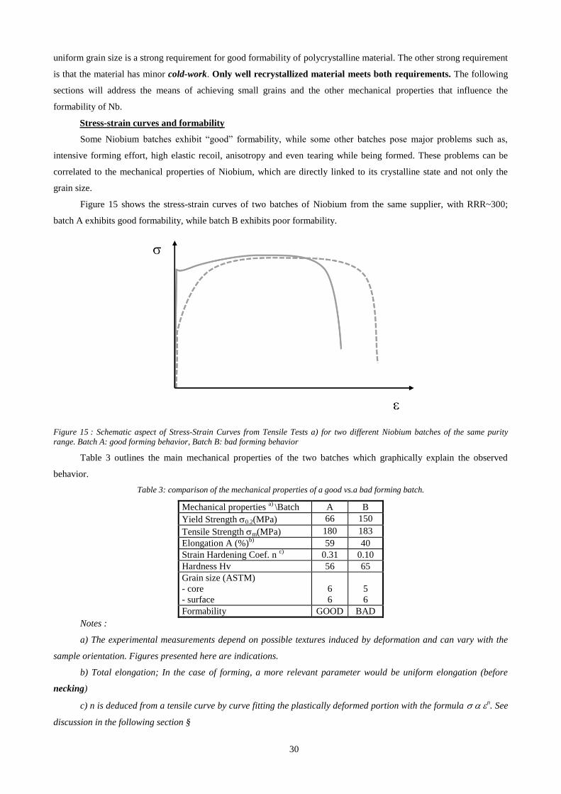
30
uniform grain size is a strong requirement for good formability of polycrystalline material. The other strong requirement
is that the material has minor cold-work. Only well recrystallized material meets both requirements. The following
sections will address the means of achieving small grains and the other mechanical properties that influence the
formability of Nb.
Stress-strain curves and formability
Some Niobium batches exhibit “good” formability, while some other batches pose major problems such as,
intensive forming effort, high elastic recoil, anisotropy and even tearing while being formed. These problems can be
correlated to the mechanical properties of Niobium, which are directly linked to its crystalline state and not only the
grain size.
Figure 15 shows the stress-strain curves of two batches of Niobium from the same supplier, with RRR~300;
batch A exhibits good formability, while batch B exhibits poor formability.
Figure 15 : Schematic aspect of Stress-Strain Curves from Tensile Tests a) for two different Niobium batches of the same purity
range. Batch A: good forming behavior, Batch B: bad forming behavior
Table 3 outlines the main mechanical properties of the two batches which graphically explain the observed
behavior.
Table 3: comparison of the mechanical properties of a good vs.a bad forming batch.
Mechanical properties a)
\Batch A B
Yield Strength 0.2(MPa) 66 150
Tensile Strength m(MPa) 180 183
Elongation A (%)b)
59 40
Strain Hardening Coef. n c)
0.31 0.10
Hardness Hv 56 65
Grain size (ASTM)
- core
- surface
6
6
5
6
Formability GOOD BAD
Notes :
a) The experimental measurements depend on possible textures induced by deformation and can vary with the
sample orientation. Figures presented here are indications.
b) Total elongation; In the case of forming, a more relevant parameter would be uniform elongation (before
necking)
c) n is deduced from a tensile curve by curve fitting the plastically deformed portion with the formula n. See
discussion in the following section §

31
We observe that Niobium of different purity but in good metallurgical condition may have a very high strain
hardening coefficient n (0,45), whereas generally that of the best batches of Nb we used was about 0,3. So there still is
room for improvement.
Micrographs and tensile curves
a) b)
Figure 16 : Micrographs of Niobium sheets (2 mm thick); a) batch A without formability problems b) batch B has a high failure rate
(high level of tearing) Note the alignments of the grains’ boundaries in case b). See text and § 2.3.3
Observe the strips of elongated grains and the big differences in grain size in the samples of batch B. In batch A
the grains are slightly bigger, and the microstructure is more equiaxial.
The above example helps determine the properties required for good formability:
- A low tensile strength, which indicates better formability
- Enhanced elongation. (The figure of interest in the case of forming is the “uniform” elongation before
necking and not the total elongation).
- A high strain hardening coefficient n (definition: see discussion below).
All these parameters vary significantly with the thermo-mechanical behavior of the material, especially, in the
case of BCC metals like Niobium. Only fully recrystallized material exhibits such properties.
When rolling is not performed efficiently, i.e. if thickness reduction is not large enough, the surface will undergo
a lot of deformation while the core of the material will be only slightly deformed. Upon recrystallization, this under-
deformed region tends to have larger grains compared to the surface region, thus leading to the features observed in
fig.5a). Thus it is very important to have a uniform grain distribution throughout the material and all grains
should belong to the same ASTM category.
Strain hardening coefficient n
When the material is well recrystallized, the yield strength of Niobium is relatively low, and there is a big
difference between yield strength and ultimate tensile strength, which gives a good deformation range. A very useful
parameter is the strain hardening coefficient n, which can be deduced from the tensile curve by approximating the
plastic part of the curve by the formula: n. In a way it represents the « curvature» of the tensile curve. The strain

32
hardening coefficient n reflects the resistance of the material to localized deformations (necking). When a local
deformation occurs, the necked region of the material is “hardened”, and becomes more (as the value of n increases)
resistant to further deformation. The deformation occurs then in the softer parts of the material away from the neck. The
higher this coefficient n, the more uniform the deformation and more delayed the appearance of localized necking. On
the other hand, if the yield strength is high, the tensile curve will be « flatter », and the risks of localized deformation
will be higher (see Figure 15).
The strain hardening coefficient is of much interest to the “deep-drawing community” ; it can easily be measured
by means of a tensile curve (uniaxial) and allows to make predictions about the biaxial deformations: indeed, it has been
shown that in case of a hemispherical shape, u varies like 4/11(2n+1) [47] – here u stands for uniform elongation. A
high strain hardening coefficient n favors bi-axial deformation, as it delays instability (necking) - for more details
regarding this calculation and its discussion, see [47]. Table 4 shows the n values of different materials found in
literature. Note that in case of a material with good formability like copper, n ranges between 0.3 and 0.45. The n values
for Niobium are in the same order as those of copper and thus Nb is expected to have a good formability too. Note that
the n values are not influenced much by the presence of impurities like O (samples 2 to 5 in table 3). On the other hand,
the n value seems to be highly influenced by the metallurgical state of the metal.
Table 4: Strain hardening coefficient of various materials
Metal n (ref [22]) Nb n
softened steel 0.15 - 0.25 a) 0.075 -
0.287
austenitic steel
18-10
0.4 - 0.5 b) 0.45
aluminum 0.07 - 027 c) 0.45
copper 0.3 - 0.47 d) 0.45
zinc 0.1 e) 0.45
nickel 0.6 f) 0.10
g) 0.31
a) Ref. [48], the same Nb material, mechanical state ranging from heavily deformed to fully recrystallized
b) ref. [44], pure Nb
c) ref. [44], pure Nb+ 80 Wppm O
d) ref. [44], pure Nb+ 230 Wppm O ;
e) ref. [44], pure Nb+ 330 Wppm O ; All samples in a well recrystallized state
f) Batch B: high failure rate when formed
g) Batch A: high success rate when formed
Note: when not explicitly found in reference, n is experimentally calculated with a graphic method described in
ref [49] where n is the slope of the straight part of the curve ln(s) =f(ln(e)).
We thus see that Niobium, of different purity, but in good metallurgical state, may have a very high n (0,45),
whereas the best batches of Nb that we used the value generally lies somewhere around 0,3. There is still room for
improvement here.

33
2.3.3 Recrystallization and recovering in high purity Niobium
Recrystallization occurs upon heat treatment following a deformation step. If the deformation is over 65%,
uniform nucleation and small equiaxial grains1 can be obtained. Recrystallization temperature will decrease with
increasing purity: it ranges from 900-1000ºC for commercial Nb (RRR 100) to ~ 800ºC for RRR ~ 300, and is
expected to be around 750ºC for RRR>400. Recovering, i.e. the reduction of dislocation density due to strain hardening
mostly occurs at the same temperature as that of recrystallization. Nevertheless recovering can be obtained at lower
temperatures without recrystallization in the case of a very slow annealing rate and long duration, or through quenching
with argon, in order to obtain a rapid cooling [50]. Recrystallization is recommended prior to any forming step as it
helps remove the effects of cold working and achieve smaller grains. An additional advantage to this heat treatment is
that it removes the hydrogen contamination that sometimes takes place during surface etching.
The deformation step prior to recrystallization is critical to achieve uniform grain size. Indeed, when
recrystallization occurs, the final grain size depends on the initial amount of deformation, as shown in Figure 17.
Indeed, dislocations tend to become denser upon strain and distribute themselves in cells that prefigure the future
grains boundary that will appear during recrystallization. Materials subjected to smaller amounts of deformation
recrystallize with very large grain compared to heavily deformed ones. This post-recrystallization property is widely
used to control grain size after a primary deformation (like rolling, cold extrusion, etc.).
Another aspect of recrystallization is that some crystallites with less hard work will fully recrystallize faster than
others, leading to discrepancies in grain size if the recrystallization is not completed.
Figure 17: Grain's diameter after recrystallization as a function of initial stress ratio .
Discrepancies in grain size in the initial Niobium sheet due to incomplete recrystallization are highly detrimental
to the forming process.
Sheets with non-uniform grain size (as the ones shown in Figure 16b) often give rise to tearing during forming
processes. Figure 16a shows a well formed material despite large grain constitution. These types of grain distribution
are directly linked to the rolling + recrystallization process.
1 Deformation and cold work introduce a lot of dislocation inside the material grains. These dislocations tend to reassemble and form “cells”
inside the grain that will initiate nucleation of smaller grains. Equiaxiality of grains is a good indication that recrystallization is completed.
Grain
Deformation

34
Figure 18 : Recrystallization curves of Niobium, obtained with Niobium RRR ~300 of grain diameter 50 µm
Figure 18shows recrystallization curves for Niobium, obtained with Niobium of RRR ~300 and grains of Ø 50
µm. The same experiment was then conducted twice, with a considerable deformation and (73%) and annealing times
of respectively 1/2 h and 1 h. Even though the annealing time does not seem to have a big influence, the temperature
proves to be of importance. All took place between 700 and 800 °C (which is in the same order of magnitude as the
temperature fluctuations inside an industrial furnace!). The results deduced from these curves, as well as the
measurements of the durations, point at a full restoration as of 800°C.
In order to be assured of a full recrystallization we therefore have to place ourselves at the end of the
crystallization, at about 800 °C. Above that, there is still some further elongation, but the ultimate strain starts to
decrease and we observe a secondary crystallization, probably related to the duration of cooling, as we did not
quench with Ar.
Further experiments with series of successive annealing/recovering allowed us to achieve deformation of the
order of 250 % (like those that arise during hydroforming) [48].
Recrystallization and actual furnace temperature:
Recrystallization and thus mechanical properties of the material are very sensitive to the temperature. It is rather
easy to get a rather uniform temperature inside a small laboratory furnace, but it is more difficult to insure it in a large
industrial installation. It will also depend a lot on the mass, shape, arrangement of the material inside the furnace and is
likely to vary from batch to batch. Measurements done in a company furnace with four thermocouples distributed inside
the furnace, showed that in some locations inside the furnace the temperature was about ~ 100 C lower than the external
indication of the furnace.

35
One way to overcome this problem is to know the relationship between time (tR) and temperature (TR) to achieve
a given recrystallization state R. This relationship is in the form of: 1
)T
1B( A tlog
R
R (9)
where time is in hours and temperature in Kelvins. A and B depend on the purity and deformation state prior
annealing, and need to be estimated for each batch of material.
Figure 19 shows an example where two sheets from the same batch annealed in different conditions but which
reached the same mean grain size. From these results we inferred the actual relationship and can use it for the following
annealing:
)T
1(10 . 3.49 10 . 8.11 tlog
R
04-04-
R (10)
Figure 19 :left hand side: Nb sheet annealed at 5 hours at 675C (courtesy of Wah Chang). Right hand side: Nb Sheet from the same
batch treated at Fermilab at 750 C, 3 hours.
For large order of Niobium, where the whole batch cannot be annealed in the same time, it is very important to
determine this relationship on small samples in a small furnace and to monitor closely the temperature inside the larger
production furnace. This procedure should allow us to gain in reproducibility and quality of the delivered material. It
has to be developed hand to hand with the Nb supplier
2.3.4 Low temperature behavior (after [44])
Little information can be found in the literature about Niobium at very low temperature. A relatively complete
and serious study was undertaken at Orsay University in the 1970’s [44]. It involved several degrees of purity and
samples that were very well characterized from a metallurgical point of view. The chemical composition of their high
purity Niobium samples was similar to that used in the cavities, but it had a smaller grain size (about 30 µm). Figure 20
shows the stress-strain curves for commercial (RRR~30) and ultrapure Nb (RRR~ 300) for temperatures between 20 K
and 300 K. A decrease in the temperature reduces the ductility of the material while increasing its yield strength and
ultimate strength. The Young’s modulus is expected to be a little higher [40], but the 10-15% enhancement observed
from stress-strain curves probably rather arises from experimental set-up.
1 “Material for high vacuum technology”, W. Espe, Pergamon Press (1966), vol 1, Metals and Metaloids)

36
a) b)
Figure 20: Stress-strain curves as a function of temperature for a) commercial and b) ultrapure Niobium (from ref [44]). Circle
shows the onset of twinning (irreversible deformation) (irreversible deformation, but the material still remains rigid). The Niobium
UP in this work has a chemical composition close to that of our Nb RRR 300. The grain size in these samples is slightly less than that
of the Niobium that we use (30 µm instead of 70µm on average). Samples section is 2 mm2.
At lower temperatures, the first steps of deformation occur by twinning (red circles on figure 7), the material is
still rather rigid, and the yield strength stays constant. At 4.2 K, fully recrystallized ultra-pure Niobium has yield
strength of ~ 400 MPa and ultimate strength of about 900 MPa [51], but these values can vary significantly with purity
or strain hardening, if present in the material. The material is brittle, i.e. no plastic deformation after twinning is
observed. Figure 21 shows the variation of ultimate strength and yield strength of Niobium as a function of the
temperature (after [44]).
Figure 21: Behavior of ultrapure Nb with temperature. Blue line: ultimate strength, red line: yield strength (dotted red: includes the
apparition of twinning: the deformation is irreversible but keeps small). N/mm2 is equivalent to MPa. After [44].
When cold the material’s resistance is much higher, but rupture occurs as soon as one passes the elastic limit.
Moreover, if one wants to be careful and not initiate twinning that will give rise to instabilities in the mechanical
behavior, it is important to stay below a certain level of stress. It is necessary to further study the cold behavior of Nb in
order to know the range of variation of these values as a function of the metallurgical state of the Niobium, so as to
Without twinning
With twinning
T( C)
(N/mm2)
Elastic
Rupture
0
200
400
600
800
1000
-270-200 -100 0 +25

37
refine the modeling of the mechanical behavior of cavities (vibration, reactions to pressure variations, Laplace forces…)
and to be protected against untimely ruptures. Recent but less thorough measurements can be found in [52, 53].
2.4. Nb sheet production
2.4.1 Example of problems in industrial production
Recently a batch of over 200 sheets was ordered, with a restricted specification that did not take the formability
into account, other than by specifying a grain size of 30 µm.
It is understandable that when one asks for smaller grains but the same purity, the manufacturer will hesitate to
completely change his way of operating. One way to achieve smaller grain without reconsidering the whole fabrication
process is to lower the restoration temperature so as to slow down recrystallization (or to shorten the recrystallization
duration). Unfortunately, these sheets appeared to be very difficult to form (more than 6 passes were necessary, large
elastic recovery, ovalization of the parts …).
A metallurgical study quickly revealed this recrystallization defect and the batch was returned for a
complementary annealing (see Figure 22). This experience underline the importance of providing relevant and yet
reasonable specifications. Too stringent specifications are not always readily achievable and will give rise to additional
cost which is not always justified by a technical improvement.
The average improvement in purity over the past couple of years comes with yet another difficulty. If one
switches from Niobium RRR ~ 30 to Nb RRR ~ 300, the recrystallization temperature decreases about 200 to 300°
lower. For a variation in purity between e.g. RRR 200 and RRR 400 one can expect differences in recrystallization
temperature in the order of 50 to 100 ° C. This asks for systematic tests to determine the right conditions for annealing,
as well as a high accuracy in the measurement of the temperature. This condition cannot easily be realized in an
industrial setting, as long as we do not make it a part of our specifications.
2.4.2 « skin-pass », damaged layer and recrystallization
Another problem is directly linked to the industrial procedure: after lamination the sheets are never completely
flat. They have to be straightened by a superficial lamination that is called “skin-pass” . This lamination has also been
used for artificially raising the yield strength, in order to comply with former inadequate specifications.
In any case, skin pass tends to concentrate damage (i.e. dislocations, displaced atoms…) near the surface (see
Figure 23).
Differential strain has very bad consequences during the recrystallization steps that will be performed
afterwards: the material is strongly deformed at the surface and much less in its core. And as we have seen before in the
case of weak deformations, we are close to the critical hardening and thus risk an exaggerated growth of the grains in
the core, while the grains near the surface keep small. This explains the « strips» of big grains that we saw in the heart
of the sheet, for example in Figure 16, § 3.2.1.
Moreover this situation is aggravated due to texture. Indeed, the texture at the core of well-crystallized Niobium
rather is type (111), while the superficial texture because of the skin-pass is more (100) like and spreads in across about
200 µm. This latter orientation does not seem to recrystallize as well as the (111) [54]. A good deal here will be part of
the famous damaged layer of 100 to 200 µm, which we have to remove from the cavity’s surface by chemical abrasion.
It also explains the patchy nature of dislocations distribution: some grains recover well during recrystallization while
some retain damage, depending on their initial orientation (see discussion § 2.6).
38
Figure 22 : Faulty batch before annealing: a) ovalization of half-cells: the diagram shows deviation from the circular expected
shape. b) the traction curves show a high elastic limit (n ~0.21-0.32) but this gets better after thermal treatment (n ~0.36-0.41). c)
Analysis of the texture shows that there are still elongated grains, with a texture at the core rather different from that at the surface.
After annealing, the grains are much bigger but uniaxial, and the texture is more uniform. Forming of the cells now can be done
without problem [55].
Figure 23: Finite element simulation of 2% reduction of 3.5 mm sheet with 1 cm diameter rolls. Strain is concentrated in the near-
surface region (red). Localized strain exceeds the average by a factor of 5. (Courtesy Non-Linear Engineering, L.L.C. and [56]).
The damaged depth may increase somewhat thicker during deep drawing. Additional thermal strain can also
appear if the welding is not properly conducted. On the other hand, a series of uncontrolled chemical polishing
(« pickling » /brightening by the manufacturer, treatments before welding…) are applied during the fabrication process

39
that can reduce it. Until now there has not been a systematic study aimed at minimizing this layer, although it might
have important consequences for the surface treatments applied to cavities for a large scale production.
Up today manufactures are still far from controlling the production of Nb in a reproducible way, and in the
context of large orders (ILC type), there is certainly reason to tighten our specifications on some realistic values and
remain highly watchful as to the material that is being delivered.
2.4.3 Damaged layer and surface treatment.
This chapter deals with the removal of damaged layer. In § 2.6 one can find a discussion of the possible
influence of damage on superconductivity.
Empirically an abrasion of at least 100 à 200 µm of the surface is necessary in order to obtain optimal cavity
performances (this need has always been attributed to damaged layer due to fabrication steps [31] without further
precision). As quoted in 1.3, two main treatments exist, namely buffered chemical polishing (BCP) and electropolishing
(EP). EP has supplanted somewhat BCP, at least in hope to reach record accelerating gradients, but is more difficult to
perform reproducibly. Huge quantity of information is available in the literature about the optimization of each process
as well as on the research of alternative “recipes”. The reader is invited to consult SRF tutorials for details. In this
chapter we will concentrate on alternatives routes seem to be the most promising in terms of costs.
Indeed, removing some hundred microns by electropolishing is costly and little reproducible. Chemical polishing
leads to a detrimental roughness and, in order to get a « smooth» surface, it is necessary to again electropolish about a
hundred µm. Something similar happens when we apply industrial mechanical polishing like tumbling. The industrial
process applied until recently left a damaged layer of about a hundred micron, as can be inferred by the necessity to
further etch the surface (EP orBCP) [57-59]. It would be more interesting to find a reliable method for the first 1-200
µm and then finish the treatment with a light electropolishing (10-20 µm).
Very recently, the tumbling process was adapted in order to reduce the damaged layer, by including some of the
features of the mechanical polishing applied in metallography and microscopy which is known to produce a reduced
damaged layer.
In the following, we will comment on mechanical polishing techniques, in particular mechanical chemical
polishing, and then how it connects to new tumbling techniques recently developed.
Mechanical and mechanical-chemical polishing
Mechanical polishing with low damaged layer as a preparation technique for metallography is a well-
documented topic (see e.g. [60]). Mechanical-chemical polishing was initially developed for the preparation of samples
for transmission microscopy where damage must be even less. The extension of these polishing techniques to large
surfaces has been developed by the microelectronic industry for the wafers 20’’ and for curved surfaces in the optical
industry. We could easily adapt this technique for application to Niobium, where its feasibility had already been shown
on small samples ([61] and [62]). We could also imagine polishing the disks before deep drawing (or the half cells
before welding) and then only apply a light final treatment.
Typically pre-polishing steps involve the use of a series of SiC papers with decreasing grain size (Ø 100 to 5
µm). The damaged layer due to each stage is more or less estimated to be 3 fold the SiC grain size. At each step, one
shall remove the damaged layer left by the previous step and leave a smaller one. Diamond is not recommended for
smooth materials. Last steps occurs on cloth with a slurry ( e.g. a colloidal suspension of silica) in presence of reactives
that tends to depassivate Niobium oxide, inducing a kind of chemical polishing similar to BCP in the slurry. Colloidal
suspensions present small grains (typically <1 µm) that tend to divide into smaller size grains upon polishing improving

40
further the polishing process with time. In some case it is possible to skip the pre-polishing steps by processing the
cloth/slurry steps for longer time.
New tumbling developments
Tumbling or centrifugal barrel polishing (CBP) was initially an industrial process. It has been applied on cavities
for decades at KEK or DESY, but was not optimized for reduced damaged layer. This topic has been resumed at
Fermilab, with extra care to use less aggressive polishing media, inspired from the slurry used in metallography.
Although the process is not fully optimized, with still a lot of intermediary steps, it was possible to prepare mirror like
finish cavities with very good RF performances after CPB and only 20 µm EP. Removing of welding defects, including
some pits seem very effective, and improvement of performance has been observed (CBP + 20µm EP showed improved
performance compare to heavy EP) [63, 64].
Performing CBP saves huge quantity of acid mixture and is preferable from the safety point of view. Evolution
of the process to hydrogen free processing, inspired by the work from Higuchi is underway [65]. Nevertheless this
process is not applicable to every cavity’s shapes. Studies should be conducted to see if the polishing step cannot be
applied initially on the Niobium sheets before forming.
2.4.4 Delivery controls and Quality insurance
Systematic delivery control is the only way to insure reliable and reproducible delivery of Niobium material.
Besides the standard metallurgical controls: visual inspection, chemical composition and RRR, tensile tests,
metallography, additional controls have been developed like Eddy current scanning of the sheets. In the previous
paragraphs we have tried to explain the physical reason at the origin of the specifications. We have also drawn attention
to factors that might need a better look into such as the monitoring of recrystallization conditions. We summarize here
the standard control operation. More details can be found in e.g. [66]. For more details concerning standard
metallurgical controls, the reader is invited to refer to handbooks (e.g. [67] or ASTM/ISO norms).
Visual inspection allows to detect defects down to 50-70 µm, either scratch or inclusions. Note that inclusions
are not likely to occur naturally in high RRR material. They are rather due to particles that got embedded in the
Niobium during processing. Indeed pure Niobium is very soft, and an industrial workshop is seldom a clean
environment.
Chemical analysis is just a control of accidental situation: standard metallurgical chemical analysis systems are
usually not sensitive enough to check the composition down to the high RRR specification. In a sense RRR
measurement is a much better probe of the purity of the material. Nevertheless in case of out of spec composition, the
detail of the composition might help determining the origin of the failure.
Tensile test are one of the most important test: if properly interpreted, it allows checking the formability of the
sheet. Points to be checked are
- small difference between longitudinal and transverse direction (strictly < 20%) for all the parameters
- relatively low yield strength, indicating well recrystallized material (typically <50 MPa, but it depends on
the grain size, and previous thermo-mechanical history of the batch)
- large difference between yield and ultimate strength, indicating a large reserve for forming
- large uniform deformation (rather than maximum elongation which is not much significant for forming).
- The 3 last points are easily determined if one calculate the stress hardening coefficient n as defined in 2.3.3.
If n>0.3, then the formability of the sheet is insured whatever the relative values of yield strength, ultimate

41
tensile strength and grain size. Since these values fluctuates a lot with grain size, n is a safer parameter than
absolute value of Y.S and U.T.S.
Metallography helps to ensure that recrystallization is complete in both rolling direction. As stretched before,
grain size uniformity is very important: grains should exhibit the same overall dimension in both direction and also over
the whole thickness of the sheet. With grain’s diameter high than 100 µm (ASTM 3.7), risks of appearance of orange
peel upon deformation are higher.
Recently an additional control, Eddy current scanning, was developed at Desy with the help of BAM institute
[66, 68]. ECS can detect inclusion about the same size as optical inspection, but in an automated and documented way.
In addition, it can detect embedded defects: embedded inclusions (although seldom expected), delamination, large
deformations. It is a very precious tool for vendors qualification.
Thorough control might become prohibitive when dealing with large batches, so once a vendor has been
qualified, we can consider taking only random sample. The statistical efficiency of such sampling is well established in
industry and can be relied on (see e.g. [69]).
2.4.5 Some comments about specifications
We hope that the previous chapters have shown what the parameters of importance for forming Niobium are:
uniformity of grain size rather than very small size, uniformity of parameters in the parallel and transverse direction: in
brief very well recrystallized state. Depending on the applications, some of the specifications currently used can be
loosened somewhat in order to reduce the costs.
For instance for simple shape like rolled, welded tubes, the uniformity of mechanical parameters is less
important, provided that the deformation is conducted along the direction that exhibit the best parameters.
When thermal conduction is very important (for instance for pieces outside the helium tank), one should ask for
a higher RRR but be prepared to receive softer material with larger grains.
If we want to increase the quality of material, there is no need to produce more stringent specifications. The ones
in use at the moment are already quite severe and not always necessary. There are numerous examples of cavities with
RRR 250-300 (or even lower) and rather large grains (50-70 µm) that have very good performances. But to our opinion,
efforts need to be put in the follow up of the industrial production of the sheets and subsequent operations. Indeed, most
of the time, the uniformity of a batch is not guaranteed. For instance, we have seen that the variation of temperature in a
large furnace, if it is not properly filled, will be large enough so that some of the sheets are not as fully recrystallized,
while others get extra grain growth. A better follow up of the production would be desirable.
High RRR (e.g. 300) material is very pure and is not liable to have large foreign material inclusion. But as noted
before pure Niobium is very soft, dust particles, in particular metallic particles as can be numerously found in industrial
plants can easily embedded in Nb during steps like rolling or deep drawing. It is mandatory during qualification of
vendors that attention is drawn on the cleanliness of all tools that will come into contact with Niobium: roller, dye,
handling tools...
Extra care must be taken on the cleanliness of tooling, which is not in the original habits of industrial production.
Lastly, EB welding of Nb is very delicate, and in the past we have observed that each newcomer in cavity fabrication
goes through a “learning curve” before mastering the welding. Since we still observe frequent problems at the welding
area (blisters and pits) a specific program dedicated to improvement of EB welding would be useful.

42
2.5. Large grain cavities:
We recently saw the introduction of a new manufacturing technique. We will briefly describe it here, as it has a
certain number of consequences that we will treat in the chapter on « morphology ». With this technique cavities are
made directly from billets obtained by EB melting: « slices » are cut from these billets that contain no more than 4-5
central grains. Indeed, after several electron beam melts under vacuum the Nb billets exhibit a very high RRR. From the
formability point of view, a fine grain material is better; indeed it is the only way to get uniform deformation and
minimum variation of thickness of the sheet. To get small grains, it is necessary to heavily deform the billets during
their transformation into sheets. This is done partially through hot forging, which also allows shaping the billet into a
shape that can be easily fed into the rolling machine, followed by several deformations/annealing steps. During the hot
forging process, which is done in an open environment, the high RRR material from the billet can be heavily oxidized
and the RRR decreases drastically.
The use of large grain or even single crystal blanks was proposed by JLab [70, 71]. This material exhibits similar
properties as fine grain material from the SRF point of view. The original motivation was to obtain material of very
high RRR at a lower price, by avoiding a large number of steps, like forging and rolling, which both have a negative
impact on the Niobium’s purity.
2.5.1 Advantages of large grain materials
By slicing directly from the initial billet one can save several steps of processing, preserve very high RRR and
save on the processing cost. Moreover, a lot of material can be saved since half-cells are cut out of disks while rolled
sheets come in square shape where corners are rejected (elliptical cavities). Multithread electroerosion techniques allow
to cut several sheets altogether with a minimized damaged layer [72].
In addition to the high RRR of the sliced material, initial studies seemed to indicate that one would be able to get
a very low roughness with a simple BCP, which would also lower the production costs [71].
Moreover cavities with large grain seem to exhibit a slightly higher Q0 value [73, 74], which could be accounted
for their high crystalline quality and their high thermal conductivity .
The use of large grain or single crystal material has nevertheless several drawbacks.
2.5.2 Drawbacks
As nearly all the mechanical properties are orientation dependent, forming can result in highly anisotropic
shapes. Although large grain material seems very ductile on tensile tests (1D deformation), as the maximum elongation
change with orientation, the actual elongation on 2D deformation is about the same as with fine grain material.
Asymmetric deformation or exaggerated thinning has been observed but can be overcome by appropriate tooling [75].
In the case of large grain material, all the grains will not deform uniformly under strain and this could result in a
phenomenon analogous to “orange peel”, i.e. steps at grain boundary. This can be overcome with appropriate
mechanical polishing, for instance barrel polishing.
Recrystallization at the welding seam is also another issue. It has been observed that no recrystallization occurs
when there is an equivalent orientation between two welded parts [76]. If no recrystallization occurs (no grain boundary
at the weld), the surface of the cavity should be very smooth even after a BCP (buffered chemical polishing), and this
would eliminate the need for electropolishing. On the other hand if recrystallization occurs, in case of BCP, we keep in
the same situation as the fine grain cavities with pronounced etching at the welding seam, and steps of several tens of
microns. Although the grain surfaces are indeed very smooth, the etching rate is different from one orientation to

43
another and it produces large steps between grains, even bigger than in cavities with « small» grains. Large grain
cavities indeed exhibit similar SRF properties as fine grain material.
The recrystallization of Niobium at a welding seam depends on the number and the orientation of the boundaries.
If two grains of the same orientation were re-welded together, there is no grain boundary after welding. The welding of
two grains with similar orientation give rise to a single boundary. On the other hand, we observe the appearance of
several grains at the welding of, for example, a triple boundary (cf Figure 24) [77, 78].
Recrystallization at welding seam is probably the reason why chemically etched large grain cavities have similar
performance as small grain cavities.
Figure 24 : Influence of the orientation on the recrystallization after welding e (Orientation Imaging Microscopy). The bi-crystal A/B
was cut along the median line. Then one of the halves was turned and re-welded [79].
Large grains cavities have a different set of balance between pros/cons compared to fine grains, and specific
solutions need to be developed if one is to industrialize production [74]. But at this stage, not much improvement of
performance can be expected on the final product.
Specific mention should be made of monocrystalline cavities (see § 2.5.2).
2.5.3 A technological exploit: monocrystalline cavities
This technique however did open a way for the manufacturing of strictly monocrystalline cavities. The first
example of cavity made out of monocrystalline sheets was done at JLab [80]. They profited from a particularly large
grain centered at the heart of the billet and fabricated a 2.2 GHz cavity, which exhibited 45 MV.m-1
after BCP. In
comparison large grain cavities treated the same way only achieved gradients about 30-35 MV.m-1
. A 1.3 GHz cavity
was realized by W. Singer at DESY, also taking advantage of a large grain at the center of the billet. Though the grain
was not big enough to fabricate a cavity, with rolling and a moderate recovering annealing he managed to obtain sheets
of the required dimension. Welding was done while very carefully conserving the initial orientation of the two half
cells, thus giving rise to a strictly monocrystalline cavity with no apparent welding seam. The results obtained are very
interesting from a fundamental point of view. Indeed, the performances of these cavities are quite similar to those of
cavities made starting from polycrystalline material, in particular in term of Q-slope: although the baking seems to be
somewhat faster, it is still necessary (see for example[71, 77, 81]). This proves that the influence of the grain
boundaries, even when it exists (we will see this later on), is not the main origin of losses observed in SRF (see
also[82]). This is surprising and important, as the effect of grain boundaries is highly influential in many other

44
superconducting applications. Monocrystalline cavities also seem to reach higher accelerating gradients than large grain
cavity after BCP, a fact that we will consider more in detail in § 3.
Unfortunately, this technique is hardly applicable to an industrial scale: a central grain in the billet is a seldom
event, and we do not master the process enough to be able to produce it on large scale.
2.6. Damage, dislocations and superconductivity
This chapter is prospective: until recently, it was very difficult to make a link between crystallographic
observations and superconducting properties of the cavities. Recent studies open this pathway. We would like to
summarize here the recent work performed by A. Romanenko and collaborators because it gives a very interesting
lighting of the possible influence of the remains of damaged layer. He worked on samples cut out of cavities (small
grain or large grain, BCP or EP) where a temperature mapping allowed to select cold and hot spots and made a
thorough comparison of hot vs. cold spot from the structural, morphological and chemical point of view [83-86].
It ensued that the main difference between cold and hot spot was observed by EBSD. EBSD is an electron
diffraction technique that probes more or less the same thickness as the field penetration depth. Indexation of the
diffraction pattern give the exact orientation of each grain, but one can also access to an evaluation of the local
misorientation and dislocation density. Romanenko observed that hot spots tend to exhibit higher misorientation angles
and higher dislocation density.
Figure 25 shows the distribution of misorientation angles for a picture formed on various types of samples,
before and after baking. Except for small grain, BCP, misorientation shifts are reduced upon baking. Small grain
cavities indeed show no improved performances after baking.
Figure 25: Local misorientation shifts in cavity samples due to mild baking. Measurements of misorientation distribution are
performed on the same sample before and after baking. Except for small grain, BCP, misorientation shifts are reduced upon baking.
Small grain BCPied cavities indeed show no improved performances after baking. (curtesy of A. Romanenko, after [84]
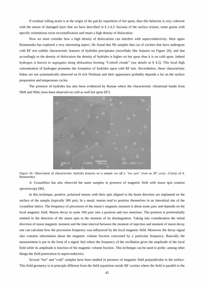
45
If residual rolling strain is at the origin of the patchy repartition of hot spots, then this behavior is very coherent
with the nature of damaged layer that we have described in § 2.4.2: because of the surface texture, some grains with
specific orientations resist recrystallization and retain a high density of dislocation.
Now we must consider how a high density of dislocations can interfere with superconductivity. Here again
Romanenko has explored a very interesting aspect. He found that Nb samples that cut of cavities that have undergone
cold RF test exhibit characteristic features of hydrides precipitates (snowflake like features on Figure 26), and that
accordingly to the density of dislocation the density of hydrides is higher on hot spots than it is on cold spots. Indeed
hydrogen is known to segregates along dislocation forming “Cottrell clouds” (see details in § 4.2). This local high
concentration of hydrogen promotes the formation of hydrides upon cold RF test. Nevertheless, these characteristic
flakes are not systematically observed on H rich Niobium and their appearance probably depends a lot on the surface
preparation and temperature cycles.
The presence of hydrides has also been evidenced by Raman where the characteristic vibrational bands from
NbH and NbH2 have been observed on cold as well hot spots [87].
Figure 26: Observation of characteristic hydrides features on a sample cut off a “hot spot” from an RF cavity. (Curtsy of A.
Romanenko)
A. Grassellino has also observed the same samples in presence of magnetic field with muon spin rotation
spectroscopy [86].
In this technique, positive, polarized muons with their spin aligned to the beam direction are implanted on the
surface of the sample (typically 300 µm). In a metal, muons tend to position themselves in an interstitial site of the
crystalline lattice. The frequency of precession of the muon’s magnetic moment is about some µsec and depends on the
local magnetic field. Muons decay in some 100 µsec into a positron and two neutrinos. The positron is preferentially
emitted in the direction of the muon spin at the moment of its disintegration. Taking into consideration the initial
direction of muon magnetic moment and the time interval between the moment of injection and moment of muon decay
one can calculate how the precession frequency was influenced by the local magnetic field. Moreover the decay signal
also contains information about the magnetic volume fraction concerned by a particular frequency. Basically the
measurement is put in the form of a signal A(t) where the frequency of the oscillation gives the amplitude of the local
field while its amplitude is function of the magnetic volume fraction. This technique can be used to probe -among other
things-the field penetration in superconductors.
Several “hot” and “cold” samples have been studied in presence of magnetic field perpendicular to the surface.
This field geometry is in principle different from the field repartition inside RF cavities where the field is parallel to the

46
surface, but we will see in § 3 that the existence of perpendicular field component is possible due to the surface
morphology.
The onset of flux entry measured by A. Grassellino strongly correlate with the onset of RF losses as measured
during the RF test by thermometry. Figure 27 shows a typical example for a sample cut out of a “hot spot”. After
baking, the onset of field penetration is shifted toward higher field for hot as well cold spots, which is very consistent
with the observation from Romanenko on dislocation density.
Figure 27: Left: amplitude of the Asymetry signal A(t) which is proportional to the volume fraction of the sample not containing
magnetic flux. When vortices start entering the sample this fraction decreases. In this example one can clearly see that baking
increases the onset of field penetration while subsequent polishing brings back the sample close to its initial behavior. On the right
hand side, the behavior of the cavity from which the sample was cut out (after [86].)
It is very difficult to evaluate at this stage what is the exact mechanism that affects superconductivity. Niobium
hydrides are poor superconductor or normal conductors depending on their exact stoichiometry. One can suppose that
they will favor preferential field penetration. Nevertheless we will see in the discussion in § 4.4 that hydrides, density of
dislocations and other types of defects are reduced by the baking in a similar way and that hydride presence might be a
collateral effect rather than the origin of losses.
This series of experimental observation show indubitably that dislocations might play a paramount role in the
superconducting behavior of Niobium, and that evaluation of their origin as studies of possible cure to lower their
density might be necessary to increase the reproducibility of cavity production.

47
3. Surface morphology and quench
Even when the dissipation phenomena at high field are poorly understood, it is relatively easy to establish the
quench: this is the generalized transition of the superconductor to normal state. The cavity then finds itself detuned and
most of the incident power is reflected. Because of the high BCS resistance, at high frequency the generalized heating
often is at the origin of the quench. But at 1.3 GHz the thermal instability can in general be attributed to the presence of
a localized defect (of the size of some 10 µm in diameter) that may provoke a localized increase in the magnetic field
and/or in temperature and thus lead to a quench. Chasing defects the size of some microns on surfaces the size of a
square meter turns out to be quite a challenge: there are a great many possible defects, but only some do effectively
influence the cavity’s functioning. Why and how? This is the both practical and fundamental issue at stake in this
chapter.
3.1. Surface morphology
Also the topography of the surface can be invoked to explain the quench, as it might locally increase the
magnetic field, for example on the steps that appear at the grain boundaries (see Figure 28). If the local field exceeds
Hc, an area of the material may transit to normal state and start to strongly dissipate. This phenomenon was originally
proposed at Cornell to explain the thermal dissipation at high field (Q-slope) [88], which later on was invalidated by the
studies on baking [89].
Figure 28 : The morphology brought about by the different surface treatments greatly depends on the initial crystalline state.
Chemical « polishing» is not a true polishing: it reveals crystallographic defects like grain boundaries or the emergence of
dislocation lines. Not all the grains etch at the same speed. Therefore steps appear that are about 20% of the size of the grains. At a
nanometric scale, though, it is not possible to distinguish the effect of one treatment from the other.
Still, this approach remained of interest to explain the quench, provided that the local increase of the field can be
evaluated correctly. The thermal calculations show that the quench is due to a localized defect with sides not bigger
than some µm, and therefore very difficult to localize on a macroscopic object like a cavity.
We therefore decided to try for a morphologic characterization of the surface, to see whether there might not be
correlation between the quench and a particular kind of surface defect. There were two problems:

48
- How do we measure the surface near a real quench, knowing that one cannot measure directly the RF behavior
of small samples1? We need to develop an in situ and non-destructive measuring technique.
- Which morphologic parameter should we consider? As we can see in Figure 29, the conventional roughness
parameters are not well-adapted to our problem; because very different profiles for the electromagnetic properties may
have the same Ra value. Nevertheless, the profile (b) should lead to a far bigger increase of the field on the peaks than
the profile (a).
Figure 29 : Two examples of surface morphology with the same roughness parameters, but a very different behavior with respect to
the EM field
Temperature maps
Several temperature mapping systems exist. Here we give the example of a superfluid helium temperature
measuring arm that was developed some years ago. It allows detecting the position of the quench in situ by means of
thermal diffusion through the cavity wall (see Figure 30). The distance between the sensors, in the order of a cm, and
the angular resolution of the motor, give a precision of 2-3 degrees at the level of the equator. Once the location of the
quench has been determined we may study the inner surface. Optical methods like endoscopy are not well adapted: at
low magnification it is not possible to distinguish a detail of a size of ~10 μm, at high magnification, there is not enough
depth of field. We therefore need to apply other methods: mechanical sensor (profilometer), electron microscopy…
without having to cut a part of the cavity! There are several methods for making replicas, but in our case it was
necessary to ensure fidelity better than a micron, on uneven surfaces. During the RF tests of the cavities we made a
temperature map in order to localize the quench, followed by making a replica at the site of the quench and at two
reference surfaces (far from the quench), to see if we could find a correlation between the quench and a certain kind of
defect or a specific morphology.
Figure 30 : Mobile temperature measuring arm and the map obtained during an RF test of a cavity at 2 K. To obtain this sort of
map, one needs to place oneself at a field just before the quench.
1 Many attempts to design cavities which could withstand samples were made. In fact, most of these cavities are at higher
frequencies and do not give a large enough precision to extrapolate to the behavior of niobium at 1.3 GHz.
T (mK)
Resistance #Angle ( )
a) b)
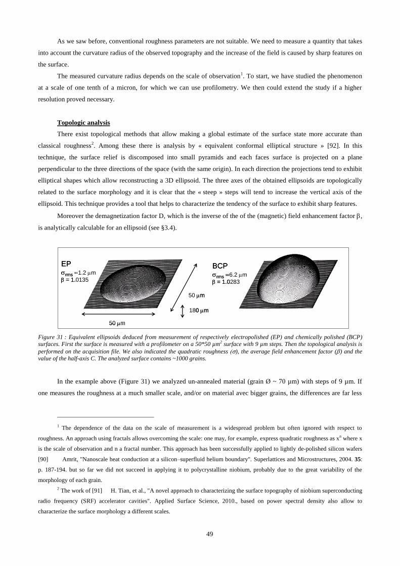
49
As we saw before, conventional roughness parameters are not suitable. We need to measure a quantity that takes
into account the curvature radius of the observed topography and the increase of the field is caused by sharp features on
the surface.
The measured curvature radius depends on the scale of observation1. To start, we have studied the phenomenon
at a scale of one tenth of a micron, for which we can use profilometry. We then could extend the study if a higher
resolution proved necessary.
Topologic analysis
There exist topological methods that allow making a global estimate of the surface state more accurate than
classical roughness2. Among these there is analysis by « equivalent conformal elliptical structure » [92]. In this
technique, the surface relief is discomposed into small pyramids and each faces surface is projected on a plane
perpendicular to the three directions of the space (with the same origin). In each direction the projections tend to exhibit
elliptical shapes which allow reconstructing a 3D ellipsoid. The three axes of the obtained ellipsoids are topologically
related to the surface morphology and it is clear that the « steep » steps will tend to increase the vertical axis of the
ellipsoid. This technique provides a tool that helps to characterize the tendency of the surface to exhibit sharp features.
Moreover the demagnetization factor D, which is the inverse of the of the (magnetic) field enhancement factor ,
is analytically calculable for an ellipsoid (see §3.4).
Figure 31 : Equivalent ellipsoids deduced from measurement of respectively electropolished (EP) and chemically polished (BCP)
surfaces. First the surface is measured with a profilometer on a 50*50 µm2 surface with 9 µm steps. Then the topological analysis is
performed on the acquisition file. We also indicated the quadratic roughness ), the average field enhancement factor () and the
value of the half-axis C. The analyzed surface contains ~1000 grains.
In the example above (Figure 31) we analyzed un-annealed material (grain Ø ~ 70 µm) with steps of 9 µm. If
one measures the roughness at a much smaller scale, and/or on material avec bigger grains, the differences are far less
1 The dependence of the data on the scale of measurement is a widespread problem but often ignored with respect to
roughness. An approach using fractals allows overcoming the scale: one may, for example, express quadratic roughness as xn where x
is the scale of observation and n a fractal number. This approach has been successfully applied to lightly de-polished silicon wafers
[90] Amrit, "Nanoscale heat conduction at a silicon–superfluid helium boundary". Superlattices and Microstructures, 2004. 35:
p. 187-194. but so far we did not succeed in applying it to polycrystalline niobium, probably due to the great variability of the
morphology of each grain.
2 The work of [91] H. Tian, et al., "A novel approach to characterizing the surface topography of niobium superconducting
radio frequency (SRF) accelerator cavities". Applied Surface Science, 2010., based on power spectral density also allow to
characterize the surface morphology a different scales.
EPrms 1.2 m
= 1.0135
BCPrms 6.2 m
= 1.0283
50 m
50 m
180 m
EPrms 1.2 m
= 1.0135
BCPrms 6.2 m
= 1.0283
50 m
50 m
180 m

50
pronounced and the measurements on etched Niobium are close to that of electropolished metal. This clearly shows that
the roughness is mainly due to differences in etching rate of the grains and to the steps resulting in case of BCP.
The values of increase of the average field (some %) are not enough to explain a quench but they give a
qualitative assessment of the roughness: obviously BCP produces « sharper» reliefs than EP. This comprehensive
approach allows for a general qualification of a surface treatment. The same approach can be used to qualify an
individual step. This has been done by INFN-Legnaro to assess the influence of distribution of steps on the field; each
step is being modeled by a half-ellipsoid. [93]. They showed that only a single step with a high form factor and placed
perpendicularly with respect to the field is needed to trigger a quench.
We arrived at the same conclusions using a 2D modeling of the field with FemLab™, but also by means of direct
measurements on a step (see hereafter).
3.2. Replicas at the quench site
To study the morphological evolution of the quench site during successive treatments, a method of replica
making proved to be the most practical. We opted for a technique validated at the University of Besancon, which
guaranteed us the desired level of reliability. This is a very inexpensive method that already has proven itself before (on
Formula 1 engines!). Following a short collaborative work to verify the validity of the method on Niobium samples, we
adapted to technique to cavities, by developing a tracking system suited to the convex and closed shape of the cavity.
This technique has also been used more recently to study etching pits found in heat affected zone of the welding seam
[94].
Figure 32 illustrates the various stages of this technique: having spotted the quench at the outside of the cavity, it
is positioned in such a way that the meridian passing through this point is in low position. We introduce a little
calibrated ball that allows us to identify the meridian and which gives us a size scale. We then, with the help of a mirror,
take a picture of the inner surface. There is a slight error due to the fact that we project a curved surface onto the plane
of the photo, but the degree of accuracy was sufficient for our needs. Next we place a soft polymer (of the « dental
impressions » type) to make a negative replica of the surface. We then transpose this replica positively on a hard
polymer, which is analyzed with a profilometer. The area we want to study is identified with the help of photos and the
placement of coordinates thereupon. As one can see on the measurements, the existence of a grain that is prominent
compared to the others is evident, although because of the lighting it is very difficult to distinguish it in the pictures.
This technique offers a significant advantage: it is very inexpensive and relatively easy to implement. It has
allowed us to open up a new direction in the exploration of the inner surface of cavities that until then had been
neglected.
From the topography of the surface, we introduced the real profile of the steps in a 2D model which allows
reproducing the local increase of the field due to the morphology. This model can still be improved, because it does not
take into account the finite size of the grain in the direction perpendicular to the field, but it allows us to assess the
overall influence of the morphology.

51
Figure 32 : The different stages in the characterization of the internal surface of cavities. Because of the artificial enlargement of the
vertical axis, the « prominent » grains are easier to highlight. At normal scale a step of the size of 10 µm on a grain that is several
hundreds of µm large is quite difficult to distinguish.
Figure 33 : Calculation of the effect of the surface morphology on the local increase of the magnetic field and the power dissipation
(see text). a) Micrograph of a cutting of the replica along the dotted line on the contour (measured before cutting). b) profile used
for calculations. c) Calculations of the local increase of the field induced by the defect. d) Power dissipation of the cavity free of
defects in green, and of the default only in blue. We see that the default becomes dominant at high field and can induce a quench.
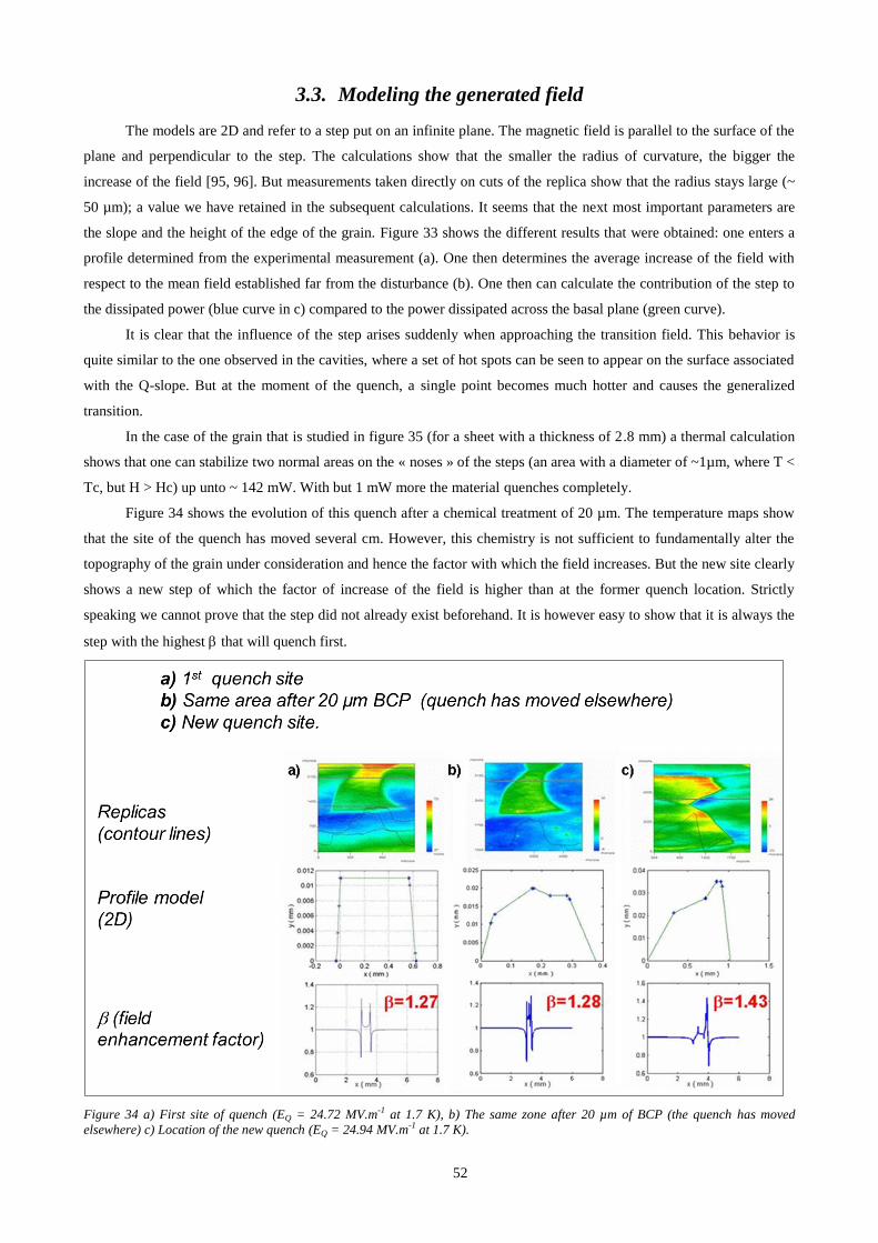
52
3.3. Modeling the generated field
The models are 2D and refer to a step put on an infinite plane. The magnetic field is parallel to the surface of the
plane and perpendicular to the step. The calculations show that the smaller the radius of curvature, the bigger the
increase of the field [95, 96]. But measurements taken directly on cuts of the replica show that the radius stays large (~
50 µm); a value we have retained in the subsequent calculations. It seems that the next most important parameters are
the slope and the height of the edge of the grain. Figure 33 shows the different results that were obtained: one enters a
profile determined from the experimental measurement (a). One then determines the average increase of the field with
respect to the mean field established far from the disturbance (b). One then can calculate the contribution of the step to
the dissipated power (blue curve in c) compared to the power dissipated across the basal plane (green curve).
It is clear that the influence of the step arises suddenly when approaching the transition field. This behavior is
quite similar to the one observed in the cavities, where a set of hot spots can be seen to appear on the surface associated
with the Q-slope. But at the moment of the quench, a single point becomes much hotter and causes the generalized
transition.
In the case of the grain that is studied in figure 35 (for a sheet with a thickness of 2.8 mm) a thermal calculation
shows that one can stabilize two normal areas on the « noses » of the steps (an area with a diameter of ~1µm, where T <
Tc, but H > Hc) up unto ~ 142 mW. With but 1 mW more the material quenches completely.
Figure 34 shows the evolution of this quench after a chemical treatment of 20 µm. The temperature maps show
that the site of the quench has moved several cm. However, this chemistry is not sufficient to fundamentally alter the
topography of the grain under consideration and hence the factor with which the field increases. But the new site clearly
shows a new step of which the factor of increase of the field is higher than at the former quench location. Strictly
speaking we cannot prove that the step did not already exist beforehand. It is however easy to show that it is always the
step with the highest that will quench first.
Figure 34 a) First site of quench (EQ = 24.72 MV.m-1 at 1.7 K), b) The same zone after 20 µm of BCP (the quench has moved
elsewhere) c) Location of the new quench (EQ = 24.94 MV.m-1 at 1.7 K).

53
The surface morphology thus explains some premature quenches observed on cavities treated by BCP, where
enhanced roughness appears close to the welding seam, due to recrystallization of large grains with different
orientations.
The influence of grain boundaries and the morphology on the field penetration has also been studied by
magneto-optics [97] and critical current measurements.
The study of bi-grains shows that indeed there is a preferential penetration of the field at the grain boundaries,
but only when the field is perfectly aligned with the boundary plane and for (static) fields much higher than the peak
fields obtained in RF, i.e., under conditions that are quite far from the configuration of the cavities. In combination with
the results on the « monocrystal » cavities, this shows that, although grain boundaries are an area of weakened
superconductivity, they do not dominate the dissipative phenomena in SRF [97].
An experiment on a monocrystal in which was deliberately dug a groove, however, shows that when the field is
applied parallel to the surface but perpendicular to the groove, a significant vertical field component appears on the
edges of the groove (see Figure 35). This proves that our 2D model is realistic. To try and quantify the influence of a
grain with finite and realistic dimensions, we also need 3D modeling [97].
Figure 35. Effect of an artificial groove on the field distribution on the surface of a monocrystalline sample (after[97]).Left : optical
microscopy and 3D profilometry. Right, up: picture obtained by magneto-optical (MO) contrast. Bottom show the schematic
repartition of field at the origin of the MO contrast.
Remark: the results obtained on monocrystalline cavities are very recent and quite unexpected. Indeed, in
numerous superconducting applications the grain boundaries exhibit a weakened or even an absence of
superconductivity, and have a predominant influence on the properties of the superconductor. We have therefore tried to
explore this aspect in some detail. We will come back to the behavior of grain boundaries in the chapter on « chemical
contamination ».

54
3.4. Welding and roughness
The grain size in fact greatly affects the roughness. Near the weld, the grains of the heat affected zone have
diameters close to 0.5-1 cm. The heights of steps as well as the parameters of the equivalent ellipsoids increase
correspondingly. The local increase of the field, in the order of 40-50%1 , starts to become significant.
Using the « ellipsoid» approach described in § we were nevertheless able to estimate the demagnetization
coefficient of a single step or a surface. Indeed, the computation of the demagnetization factor for an ellipsoid is
relatively easy:
m
m
m
mDa arccos
11
1
1
22 (11)
Where m = c/a
Table 5 shows the evaluation of the demagnetization factor estimated
after the ellipsoids parameters as directly measured on surfaces with various roughness characteristics. Note that from
the topological point of view, a hole is equivalent to a protrusion. So the same approach can be used to study etching
pits.
Table 5: Roughness parameter and demagnetization C factors for ellipsoids measured on standard surfaces.
Parameter
Small-grained
material
Annealed,
far from the
weld
Thermally affected zone
(near the weld) Mean value
Weld defect*
C~ 50µm
2A~200µm
Etching (BCP) Electropolishing (EP)
grains 70 µm 1-2 mm 0,5-1 cm 1 mm => 1 cm -
Ra 1-2 µm 4-8 µm 40-80 µm ~ 1 µm -
C ~ 300 ~ 90-100 ~ 350 ~ 70 50
=1/D 1,065 1,028 1,4 1,018 1,9 !!! *
*Defect associated to a hot point on a cavity quenching at 15 MV.m-1 observed at Fermilab [94, 98] (cf Figure 36)
These simple calculations can also be confirmed with finite element approach. Figure 36 shows the modeling of
an ellipsoid of similar dimension and shows similar modeling for a sharp edged fracture. Here again we can observe
that the most important part is the sharpest curvature area.
1 The factor of increase of the field has been calculated for this region by two different methods [78, 85]. These,
however, are 2D methods, that necessarily overestimate the influence of the step.

55
Figure 36 : Finite element simulation of the field enhancement factor for an ellipsoid 50µm x100 µm (courtesy of Z. Insepov).
Figure 37 shows the same kind of modeling for cracks generated on RF copper cavities (in this case to probe the
field emission potential of such a crack). The same calculation applies for magnetic and electric field enhancement.
Similar 3D simulation have also been conducted at Cornell [99]and show that field enhancement factors between 1.5
and 2 can be easily reached in defects very small compare to cavity size.
Figure 37: Finite element simulation of the field enhancement factor for surface cracks (courtesy of J. Norem,
arxiv.org/pdf/1108.0861).
In the case of electric field enhancement of a factor 50 -100 are often necessary to model field emission, and it is
doubtful that surface morphology plays an important role, whereas magnetic field and enhancement of a factor 2 will
have strong consequences on the transition field.
As we will see in § 7.1, the surface morphology does not matter much for field emission whereas it can be the
dominant effect for quench apparition.
The cavities treated by electropolishing, followed by a moderate baking, show quench thresholds that are
systematically higher than those of cavities treated in a conventional way, by chemical polishing and baking (resp. 35-
40 MV.m-1
and 25-30 MV.m-1
). Only some individual cavities (in thousands of tests) succeeded in reaching ~40 MV.m-
1 after chemical polishing, without the possibility to check the reproducibility of this result. Among these were mainly
~ 5

56
seamless cavities or without boundary (cavities prepared by hydroforming or spinning, monocrystalline cavities) [100,
101].
It is therefore that we believe that all the techniques that maintain welds and grain boundaries are likely
to give rise to a premature quench in case of BCP treatment. « Large grain » cavities do not come with any
particular advantage in case of BCP surface treatment, except in terms of the cost of the Niobium supply.
Electropolishing does not make disappear all the steps on the surface, but as the curvature radius on the steps are much
larger, the field enhancement factor is not so high. That could explain the relative better results obtained with this
surface treatment.

57
4. Chemical contamination at the surfaces / interfaces of the Niobium
It is important to recall that in the penetration depth of the magnetic field currents circulate of the order of some
1012
A/m2, being 50 to 100 nm for Niobium. It is in this part of the superconductor that the dissipative phenomena
originate.
Several indicators highlight a possible influence of the chemical composition of the surface, because cavities
treated by electropolishing have behaviors that are slightly different from those treated by chemical polishing. Most
obvious is the difference of the quench threshold, but we saw in the previous paragraph that this might be an effect due
to the surface morphology. There are however some differences: surface resistance after baking, surface magnetic
field… which could be attributed to a difference in composition. In this chapter we therefore look at chemical
contamination at the interfaces (i.e. the surface and the grain boundaries).
When dealing with thicknesses of some nanometers, getting a precise overview of what happens at the surface
with only one or two techniques is illusory. To make sure to get a correct idea of what happens one need to cross
several techniques, and make sure that the analysis of the results is made by experts aware of the particularities of each
technique. Indeed, the interpretation of surface analysis is not always straightforward and requires a good understanding
of the physical and technical limitation of each technique.
All the results presented here after have been gathered through several collaborations, where the experts of each
technique have been involved in the interpretation of the results. Collaborating with several laboratories allows getting
results that are far more complete than those obtained by focusing on a single technique. Given the inherent difficulty of
the problem (study the interface under the native oxide layer), an approach from several angles allowed for the
corroboration of less certain results.
4.1. Surface composition and oxide-superconductor interface
The mechanism of chemical or electrochemical polishing is similar to a phenomenon of corrosion, where the
formation of an oxide and its dissolution compete (see appendix 7.3). At the time of the formation of the oxide layer,
other atoms (e.g. O, H ...) may spread and pollute the first metallic layers at a depth that seems to be comparable to the
depth of penetration of the magnetic field. Until recently there was no theoretical model for the influence of such a
contaminated layer on the superconducting behavior. But as superconductivity is a phenomenon related to the
crystalline lattice, one should expect each defect therein to have some influence. What counts, however, is succeeding
in quantifying it, for example by correlating levels of impurity and a specific behavior of the cavity.
Studying this layer at the interface oxide-metal is very difficult: indeed, there exist highly sensitive techniques
with a very good depth resolution, but which are particularly sensitive to the outer layer. The most external layer (oxide)
does not play a direct role in radio frequency (it is a good dielectric, transparent to the RF wave). The layer that interests
us is buried under 4-5 nm of native oxide and the usual layers of contamination (hydrocarbons, H2O ...). Only
techniques that have excellent depth-resolution or that provide chemical information allow distinguishing between the
contamination that interests us and the more superficial one that doesn’t seem to play a role of importance in SRF. The
study of oxide and the oxide-metal interface, however, gives us paramount information, as the oxygen is the Niobium’s
main impurity. These studies have also shown that our material is far from uniform at the nanometer scale.
Here are the limits that we will face:
Most of the common techniques (e.g., electronic probe, EDX, X-ray diffraction) explore a volume too deep
to be sensitive to these very superficial effects, i. e. concentrated in the first nanometers of the surface.

58
An additional difficulty for the profiling techniques by abrasion is that the oxygen is preferentially sputtered
in the Niobium oxides. Only techniques where the rate of abrasion is very slow and very well controlled can
give us the necessary resolution (e.g. TOF SIMS). The angularly resolved techniques can also give us valid
information, but they are generally limited in depth.
Very local techniques, such as TEM, also come with a problem of size: how representative is what we
observe at a very local scale? Only a large number of measurements (which is not always possible if one
uses very heavy techniques) can allow for an overall vision.
A technique like XPS (also called ESCA) is very interesting, because it provides information on elements
and their chemical environment – a good way to distinguish interstitial oxygen that oxygen in the oxide for
instance. Unfortunately it is not very sensitive: 0.1 At % at best.
Most of the observations presented below were made on sheets identical to those used for the fabrication of the
cavities, because we wanted to observe samples that are representative for our material. However, we did notice that
some changes observed after different treatments applied to the Niobium are generally of the same order of magnitude
as those observed simply by displacing the probe along the surface of a polycrystalline sample. In order to remove some
of the ambiguities of the observation we have therefore, whenever possible, opted for the study of monocrystals of
different orientations.
4.2. Hydrogen
4.2.2 The « 100K » effect or « Q-Disease »
In the early 90s we were confronted with huge fluctuations in the results of the cavities, without being able to
find out why. Following a defect in the cryogenics during the end-of-the-year holidays, the performances of an
accelerator in Wuppertal became totally degraded, even though the temperature had risen by only some tens of K. At
such a temperature only few species are still mobile and we began to suspect the hydrogen, capable of forming non- or
only weakly superconducting hydrides, even at low temperature.
The presence in the Niobium of hydrogen in solid solution is the result of corrosion phenomena mainly caused
by surface treatments and the room humidity, but its low concentration seemed insufficient to explain the degradations
of Q0 that were observed in some cavity tests.
Figure 38: Effect of slow cooling on a cavity, before (white dots) and after annealing (dark dots).

59
The surface analyses have then shown that the hydrogen segregates at the metal-oxide interface. There the local
concentration may become sufficiently high (~103 to 10
4 At.ppm) for the formation of one or more hydrides (NbH,
Nb2H, Nb4H3, NbH2) at temperatures between 80K and 150K. The critical fields of these hydrides are weak compared
to that of Niobium, and they transit to normal state (dissipative) as soon as the field is increased in the cavity. This
explains the dissipation observed at very low fields (Figure 38, light curve). We can prevent the kinetics of hydride
formation by means of quenching around 100K (very fast drop in temperature), which sometimes was applied during
cryogenic testing and explains why at first the effect seemed pretty much random: all depended on the « urgency » of
the experiment! This, however, is not feasible in the case of an accelerator (high thermal inertia).
The solution is to evacuate the hydrogen by means of a thermal treatment (typically 2h, 800°C -Figure 38, dark
curve- or equivalently 10h, 600°C).
This treatment does however come with certain disadvantages. A short etching (<5 µm) is needed to get rid of
diffusion layers (oxygen and carbon); it is only a temporary solution, as the Niobium after being exposed for several
months to the room humidity will again be loaded with hydrogen [46, 102, 103]; and its industrial costs are high. With
the generalization of electropolishing that, as it is currently being practiced, causes heavy hydrogen pollution, this topic
of study has come back forefront. It is important to list the research techniques that could be applied to the subject, as
well as the limitations in their use, and focus on the steps that are especially polluting.
4.2.3 Experimental observations
Most of the experimental work presented here comes out of [102, 104, 105]. Figure 39 shows the results of
surface analyses of different samples by means of HFS. Under the conditions of this experiment this technique has a
resolution of about 30 nm1. Therefore we could not distinguish between the superficial contamination (hydrocarbons)
and the interstitial hydrogen in the surface peak, but the figures of the 30-300 nm slice are undeniable: the quantity of
hydrogen close to the surface is ~1000 time the bulk content. Analysis shows that a significant amount of hydrogen
returned to the surface after 18 months of exposure to air. This behavior has also been observed with other techniques
[103]. But this is not insurmountable in the case of an accelerator: most of the time the cavities are kept under vacuum.
In the right part we also see that material that is well crystalized compared to ordinary material appears to be far less
sensitive for contamination. Indeed, hydrogen tends to gather around dislocations to form Cottrell clouds [106].
Annealing the material not only rids itself of hydrogen, it also reduces the dislocation density and makes the material
less sensitive. We observed a similar behavior on the cavities: after thermal treatment, in case of prolonged chemical
treatments, the 100 K effect reappears, but is less pronounced.
We also gave special attention to pollution caused by electropolishing, which at present is the recommended
treatment for the cavities.
The study of the contaminating steps confirmed that this pollution mainly occurred without bias and not during
the electropolishing itself. Indeed, HF, and in a lesser extent HCl are known to depassivate the oxide layer, removing its
protective effect of diffusion barrier to atomic H..
1 Better resolution is now available with more recent set-ups, but this technique is still very sensitive to surface roughness.

60
Figure 39: Left: ERDA spectrum of an Nb sample before (H) and right after thermal treatment (F): the peak observed on the surface
can be partially attributed to the usual hydrocarbon contamination (see the sample of Si used as a reference for surface
contamination). In the core of the material the amount of hydrogen is below the limit of sensitivity (0.1% At), but near the surface
there was about 10 000 times more hydrogen than the amount measured on the bulk material. Right: influence of the crystalline
state: down re-crystallized sample (annealed), and up, ordinary material. Both samples were soaked for 10 days in a HCl solution to
charge them with hydrogen.
The mechanisms of apparition of H. during acidic processes are reviewed in details in [107]; four types of
reactions are involved and/or competing, and the effective pollution results from the balance between these different
reactions:
(1) Volmer process (fast):
M + H3O+ + e
-(M) ↔ HadsM + H2O
(2) Heyrovsky-Horiuti process (slow):
M + Hads + H3O+ + e
-(M) ↔ 2M + H2 + H2O
(3) Tafel process (slow):
HadsM + HadsM ↔ 2M + H2
(4) absorption process, competing with (2) and (3):
HadsM ↔ HsM
where Hads represents hydrogen, in the atomic form, adsorbed on the surface of the metal, and Hs dissolved (=
absorbed) under the surface of the metal.
In presence of very oxidizing species like NO3-, it is well known that the product of the reaction (2) is H20
instead of H2, a fact which explains why molecular hydrogen (H2) release is not observed in presence of HNO3. For
instance, the global reaction (1) + (2) could write (5):
HadsM + 2H30+ + e
-(M) + 2NO3
- ↔ 2M + 3H20 + 2NO2
Process (4) is probably the main source of H interstitials. Molecular H2 is less likely to be a source of dissolved
hydrogen since it has to dissociate first, before diffusing inside the metal. More detail about the thermodynamics of H-
Nb system can be found in [108]. Measurements and measurement techniques can be found in [104, 105, 109, 110].
Nevertheless, our study also showed the great sensitivity of freshly etched metal to gas bubbles, which is
understandable because the oxide is partially dissolved by HF (one needs to apply a Teflon fabric to prevent bubbles
from reaching the Niobium surface). A more surprising results was the massive pollution brought by hot water rinsing
(>80°C), which has led us to abandon this method of rinsing [105].

61
4.2.4 Surface segregations and pure metals
Somewhat paradoxically, surface segregations will rather be observed in ultrapure metals. They originate in the
interactions between the impurities and defects in the lattice, through the lattice’s elastic deformations. The energy of
these interactions shows an increase from a point defect (e.g. vacancy), to a linear defect (e.g. dislocation), and then on
to a two-dimensional defect like a surface or interface. When there are few defects in the matrix, as is the case of pure
metals, the metal-oxide interface is the metal’s main flaw. It is therefore not surprising that we find segregations there.
Hydrogen is very mobile at room temperature, but we may explain its presence in high concentrations near the surface
by an analogy with the atmosphere: although air molecules are completely free to move, the atmosphere is denser at sea
level than at higher altitude, as the effects of gravitation add up to the scattering effects.
The existence of segregation near the surface suggests that similar phenomena might occur at the grain
boundaries. We already discussed this in the « morphology » chapter and will come back to the contamination aspect
below.
Note that some of the hydrogen can also be trapped by vacancies, especially if close to another impurity
interstitials [107]. Each oxygen, nitrogen or carbon impurity traps only a single hydrogen atom under formation of
oxygen-hydrogen, nitrogen-hydrogen or carbon-hydrogen pairs, where the trapped hydrogen occupies interstitial trap
sites in the neighborhood of the trapping impurity. The trapped hydrogen is also located on tetrahedral interstitial sites
[111]. There are direct evidences that hydride precipitation is inhibited due to trapping at O and N interstitials [107,
112]. Moderate heating like baking can detrap hydrogen as inferred from the large augmentation of vacancies
concentration after baking [113].
4.3. Other surface contaminations
The study of surface contamination by several additional techniques also has brought to the fore the segregation
of hydrogen, carbon, and the presence on the surface of other species, originating in the bath of chemical polishing like
F, P (in the form of POx, x=1 to 4) or S (Sox), depending on the surface treatment. The oxygen and carbon at the
interface metal-oxide are very difficult to study because of the presence of a surface layer (oxide, hydrocarbons) that
sometimes masks the signal of interests (the one that originates from the superconducting matrix). For oxygen, for
example, most of the conventional techniques cannot distinguish the chemical form of oxygen: oxide or interstitial. The
case of oxygen will be treated in more detail in the chapter below but we can already recall that it may be found in the
form of interstitials at the metal-oxide interface. In several works, the difference between the oxygen of the oxide and
interstitial oxygen in Niobium metal was clearly established. A measurement shows that there is about 200 times more
interstitial oxygen near the metal-oxide interface than in the bulk of the material. Earlier studies have shown
segregations of other impurities (H, C, F, P, S, ...) at the metal-oxide interface. [114-120]. This region is where the
highest current densities circulate. Defects of the crystalline lattice and impurities are known to affect the bulk
superconducting properties of Niobium. For instance interstitial atoms are known to decrease TC, but in the case of
surface contaminants, it is difficult to precise the exact role of each impurities. Only a comparison of the same treatment
on cavities and on samples can allow us to establish the influence of the different contaminants evidenced by surface
analysis by making a correlation with actual cavity results.

62
4.3.2 Contaminations at the metal-oxide interface
By combining several techniques, we are able to identify these segregations. The main difficulty, as noted, is to
determine the location of the interface. The depth calibration is sometimes difficult, especially because the metal-oxide
interface is not uniform (see next paragraph).
Figure 40 shows two typical surface contamination patterns, obtained by Glow Discharge Spectroscopy and
SIMS. In the case of GDS we can clearly distinguish a C and H signal on either side of the oxygen signal (in blue). The
most superficial signal can be attributed to hydrocarbons outside of the material. The deeper contamination signal then
appears clearly just after the signal caused by oxygen.
Figure 40 : Profiles of surface contamination on Niobium obtained by (a) glow discharge spectroscopy (GDS) and (b) SIMS. The
intensity of the signals in such techniques is arbitrary unless compared to a known standard. As the signal is proportional to the
atomic concentration it can be used for relative comparison and profiling information. In the case of GDS, we can clearly distinguish
a signal C and H on both sides of the oxygen signal (blue) In the case of SIMS depth was calibrated using a thin Niobium sample
prepared by MBE and of known thickness. The thin line corresponds to a sample prepared by EP and the thicker line to a sample
prepared by BCP. In both cases one sees that the contamination penetrates to ~ 10-20 nm in the heart of the material. (NB. The
signal intensity is relative for the GDS and absolute for SIMS. In both cases the units are arbitrary. The surface is to the left and the
heart of the material is to the right).
In the case of SIMS the depth was calibrated using a thin Niobium sample prepared by Molecular Beam Epitaxy
(MBE) and of known thickness. In Figure 40b, thin lines represent a sample prepared by EP and thicker lines a sample
prepared by BCP. For these two techniques it is difficult to assess the absolute amounts, because near the surface
sputtering rates are poorly established. They do allow, however, the relative comparison of samples prepared in
different ways.
Figure 41 : SIMS imaging of the surface: we see that there are inclusions rich in oxygen and carbon, which appear below the oxide
layer. Such micro-porosity are believed to appear during cool down of the melted billet: light elements like carbon, oxygen,

63
hydrogen… tend to reassemble in the liquid phase where they get concentrated during the solidification process, leaving a kind of
“blister”, when the material has become entirely solid. Upon forging and rolling, these blister sides become deformed and irregular.
In most cases we find a penetration of the contamination by approximately 10-20 nm, into the core of the
material. For oxygen, the diagnosis is more difficult. Only a parallel study with other techniques (XPS, diffuse
scattering ) allowed us to formally demonstrate the existence of interstitial oxygen (see next §).
This pollution is probably not uniform: in fact, as shown in Figure 41, if we make an image of the surface by
SIMS, we see that there are areas, of a few square micrometers in size, with a high concentration of carbon and oxygen.
This effect has also been observed by SEM and by nuclear microprobe. [121]. Probably we have to do here with micro-
porosities; we have not observed any significant direct influence of these small defects, but they may be causing hot
spots that appear on the surface at high fields and whose position seems to fluctuate with the etchings.
Note that V. Palmieri proposed a model of a 2-layer superconductor, and found that the results are consistent
with the observed behavior of cavities, notably in terms of low and medium field Q-slopes [122]….
64
4.3.3 Oxidation of Niobium
RRR 300 Niobium is covered with a natural defective oxide, namely Nb2O5-x with x varying slightly depending
on its formation conditions. When grown in wet condition, the oxide tends to incorporate anions from the solution as
minor impurity.
Numerous studies of the influence of different stages of the cavity preparation on the nature of the oxide have
been conducted, in the hope of being able to highlight phenomena that can be linked to the behavior of the cavities. This
research together with some more recent experimental facts allows showing that the oxide plays a minimal role in the
observed dissipations. We will present these results here, even if they are not directly related to the superconductivity.
Niobium is a valve metal that very quickly becomes passive at room temperature, but readily reacts with light
elements as soon at it gets rid of its protective oxide layer (e.g. upon heating). The thickness of the native oxide of
Niobium (in equilibrium, exposed to the air) is on the average 5 ± 1.5 nm, but depends on the crystal orientation of each
grain (results obtained by ARXPS [116, 123-125] and MET [126]). In our case oxidation starts during the chemical
treatment (BCP or EP), continues during the rinsing steps, and ends with the exposition to the air humidity. (For
Niobium, water is a more effective oxidant than O2 from the air). The growth mechanism is of the Mott-Cabrera type,
which means that electron pass freely from the metal to the oxide surface where they ionize the oxygen atoms. This
establishes an electric field through the oxide which drives a slow ionic transport across the oxide film [123, 124, 127].
The first oxidation steps obviously have an influence on the nature of the oxide and one can therefore wonder
whether they will also influence the underlying superconductor.
For example, using TOF-SIMS it is possible to show the incorporation of SOx anions in the oxide samples
prepared by EP (with sulfuric acid in the solution), POx anions in the oxide of the samples prepared by BCP (with
phosphoric acid in the solution) [116, 117, 126, 128, 129]. This pollution remains however rather weak: with XPS it is
not detectable, which means that it is probably below 0.5 atomic %. This incorporation of anions is a well-known
phenomenon for many metals [127, 129]. For Niobium these ions of tetrahedral form replace NbO2 of the same
geometry [130].
The microcrystalline-amorphous structure of the Niobium oxide Nb2O5-x is very special: it consists in more or
less regular stacks of NbO3- octahedron, with alternate stacks of « defects » (Niobium with coordination number 4,
NbO2) that allow to recover the stoichiometry. By varying the size of the different stacks one may accommodate more
or less of the stoichiometric defects. Oxides prepared in wet condition apparently show more defects than oxides
prepared in dry condition (Figure 42, after [123-125]). From the electronic point of view, this oxide present a
semiconductor structure with a relatively large gap (3.4-5.3 eV [131]), but the defects of the structure act like trap inside
the forbidden band and allow a certain amount of electronic conduction via a hopping mechanism [132] the more
defective, the highest the electronic as well as the ionic conductivity [127]. So when the oxide gets degraded upon
annealing, more and more defects appear in the forbidden gap, and the conductivity of sub oxide increases. At the end
of the sub-oxide series, NbO, traps are so close together that they form a continuum, and the conduction becomes
metallic.
The HPR (high pressure rinsing) also brings certain changes: it allows for a notable increase in the thickness of
the oxide layer and for a decrease of the quantity of Fluor near the surface. The source of the Fluor is HF contained in
the two solutions (EP and BCP) used to un-passivate the surface. In fact, only the NbF5 complex is soluble and allows
dissolving the Nb5+
. The Niobium oxide therefore gradually is transformed into oxyfluorides, up to pentafluoride, which
then dissolve. Less soluble oxyfluorides are likely to remain on the surface of the Niobium when it is taken out of the

65
acid. They will be incorporated into the oxide during its growth, until it has reached its equilibrium thickness. This has
been observed with XPS as well as with SIMS [115-117].
Figure 42 : Amorphous-microcrystalline structure of Niobium oxide Nb2O5-x. This is more or less regular stacks of NbO3—
octahedron, with stacks of « defects » (Niobium with coordination number 4, NbO2) which allow to catch up the stoichiometry. By
varying the size of individual stacks one can accommodate many stoichiometric defects. Figure prepared using [133] and [125, 134]
The fact that the oxide does not attain readily its equilibrium thickness seems to contradict earlier published
results [123-125], which show that in the presence of water this equilibrium is reached within minutes. We now use,
however, a Niobium that is far more pure and better crystallized. It is not surprising that a growth mechanism involving
vacancy hopping will be slowed down in a material with fewer defects.
The growth of the oxide then continues in the air, and exhibit a rather surprising phenomenon: the growth of the
oxide is much slower after electropolishing than it is after chemical polishing (Figure 43). The oxide is of the same kind
(pentoxide), but the difference resides in the impurities (incorporation of anions). We believe that here also the density
of the defect in the oxide is not the same in the two cases.
This difference in growth rate is probably at the origin of the slight excess of oxygen that is observed under the
electropolished surfaces (unpublished observations by SIMS, also seen by AES [135] and inferred by magnetometry
[38], but the depth resolution of these techniques does not allow to locate it precisely).
We have also observed a similar growth delay after a simple rinsing with HF: more than 48 h after the HF
treatment (followed by H2O !) the oxide was still present in the form of a mix of NbO et NbO2 [136]. This kind of
rinsing is regularly applied to cavities in case of field emission: it helps to dissolve dust particles on the Niobium
surface – as well as the underlying oxide – but it does not affect the metal, hence does not affect the cavity’s
PO43- SO4
2-
NbO2 NbO3-
Valence/Coordination rayon ionique
Nb(V) Td (4 neighbors) 0.62 Å
Nb(V) Oh (6 neighbors) 0.78 Å
S(VI) Td (4 neighbors) 0. 26 Å
P(V) Td (4 neighbors) 0.31 Å
O(-II) Td (4 neighbors) 1.24 Å
O(-II) Oh (8 neighbors) 1.28 Å
66
performances. The time between the preparation of the cavity and its test in general will be between 24 and 48 h. It was
thought that the rinsing with water allowed reconstituting the pentoxide and its good di-electric properties. But
apparently, even if the oxide is not of good quality, there is no notable difference in the cavity’s behavior, which proves
that the observed dissipations come from the interface and clearly dominate any possible dielectric losses.
Note also that the thickness of oxide after EP can vary a lot, depending on what voltage was applied when the
process was stopped, and how long did it stay in presence of HF. Indeed if the voltage is high, then the thickness of the
oxide can increase due to a mechanism similar to anodization. Then once the voltage is stopped, the oxide layer gets
dissolved by the HF present in the solution. In most of the time, it take a while to remove the acids, and the oxide gets
thinner, but on samples it has been observed that it sometimes can be thicker than 6 nm.
It therefore became crucial to study this interface. There one finds an NbO layer (metallic and the interstitial
oxygen.
A lot of photoemission publications have been dedicated to this topic, which we think is a very delicate one:
finding out a very weak signal by deconvolution in a spectrum is not enough to establish the existence of the species
under consideration. The fact that a deconvolution calculation can “detect” the presence of a fraction smaller than 10%
is far from enough to establish its existence from a single photoemission spectra (a step to often taken in many
publications). Smaller fraction need to be established through careful crosschecking and sufficient statistical data to
reduce the uncertainty of deconvolution to an acceptable value. Here below are two examples of approaches that allow
determining significant data on lower fractions: namely NbO and metallic Niobium in contact of interstitial oxygen
Nb0(Oi).
Taking a synchrotron light source for a better energy resolution, combining several detection angles and several
incident energies, and deconvoluting all of the spectra together rather than a single one, we can hope for a more reliable
result. In order to get a good energy resolution, however, we need to keep relatively weak incident energy, and thus an
escape depth of the electrons that is rather small. We had to work on samples annealed at 2000 ° C under UHV to get
rid of the pentoxide. These samples still have a monoxide layer on their surface, and although much oxygen is being
desorbed during annealing, we found that the 3 upper nm of the surface had about 10% of oxygen atoms, which is about
200 times more than what is contained in the bulk (Figure 44).
On the other hand, it has been established that during the oxidation of Niobium in the presence of moisture, there
is a strong competition between injection of oxygen atoms and oxidation. In certain cases up to 70% of interstitials can
be found under the oxide layer (the proportion of oxygen atoms in Nb2O5 is 71,42%) [137].
The other technique is principal component analysis (PCA): a technique now commonly available on most
modern analysis set-ups.

67
Figure 43 : XPS spectra of the doublet of Niobium for various stages of treatment. The two right peaks correspond to the metal
Niobium and tend to disappear when the oxide thickness increases (left peaks). A careful deconvolution could give us additional
information on the intermediate oxides that are present in very small quantities [117, 138].
Figure 44 : Advantages and limitations of the photoemission (XPS). This technique is the only one that provides chemical
information, but it is little sensitive (typically 0.1 atomic%) and very limited for the minority species that interest us. By combining
different energies and different measurement angles, one can nevertheless get information on the depth [139, 140] NB.. Ionic
sputtering to obtain a profile is not recommended for Niobium because of preferential sputtering of oxygen.
In PCA one brings together a great number of spectra, whose points are considered as so many matrix elements
and then one searches the eigenvectors of this matrix. Each component’s is then classified depending upon its statistical
weight. It is usually accepted that only component with a weight superior to 10 % are valid. The number of component

68
with a realistic statistical weight is equal to the number of different atomic species in presence. Note that each
component determined this way is an independent linear combination of the individual spectra of each species, but not
the individual spectra themselves. .In case of uncertainty, more statistics is needed.
Figure 45 shows a series of 40 spectra taken in situ during the baking of a Niobium sample. On can observe
clearly that the doublet corresponding to Nb5+
(pentoxide) decreases while the doublet corresponding to metallic
Niobium increases, which indicates that the oxide layer is getting thinner during vacuum baking. But one also observes
several intermediate species (suboxides, as indicated by arrows). Unfortunately the XPS is not precise enough for us to
quantitatively assess whether the oxygen is re-injected into the underlying metal matrix or not.
The PCA analysis shows that 6 different component seem to be significant. One can infer that the four strongest
signals are likely due to species already listed in Niobium: Nb0, NbO, NbO2 and Nb2O5. The two weaker signals,
however, are probably related to the presence of atoms of the metal with a nearby interstitial. (Strictly speaking it is
difficult to know whether it is oxygen or another light atom, but O is nevertheless the most common impurity and the
most likely.).
Figure 45 : left: series of 40 spectra obtained in situ during the vacuum baking of a sample and right: principal component analysis
of this series. One can see very clearly that there are no more than six components with a statistically significant weight. Study done
in collaboration with l’INFN-Genova [118, 141].
As far as we know this technique is the only reliable method to demonstrate the existence of species in very
small quantities with conventional XPS.
These results added to those discussed in the paragraph on baking (e.g. magnetometry) allow us to establish that
there is indeed a layer of interstitials of some nm just below the surface, with oxygen atoms in concentrations of some
tens of atomic percent’s.
4.3.4 Baking: hunting for interstitial oxygen
The existence of this interstitial oxygen initially was considered as a possible explanation for the baking effect:
indeed, one can imagine a scenario where there is pure Niobium covered with a highly polluted thin layer (few nm).
The superconducting gap would be affected at the surface, there where the field is the strongest. This could explain the
dissipation at high field, a degradation of 10-15% of the gap resulting in a 10-fold increase of RBCS. Also, as soon as we
increase the field this layer transits and begins to dissipate even more. After baking the oxygen would have been

69
distributed more evenly and we would find ourselves in the presence of a Niobium only slightly degraded (see the
diagram in Figure 46). This would be consistent with the experimental observations of the modified mean free path and
the gap 1
.
Figure 46 : Possible scenario explaining the effect of baking.
Additional arguments support further this scenario. Heat treatments performed at different temperature show that
there is an optimum temperature. At lower temperature only the initial interstitial oxygen atoms diffuse whereas at
higher temperature the oxide layer gets discomposed between 200°C and 300°C and eventually the oxygen diffuse
inside the material [142-144]
The study of SIMS spectra before and after baking indeed show slight changes in the oxygen distributions near
the surface, but also those of carbon, fluor and hydrogen. Several problems, though, prevent us from drawing clear
conclusions from these results:
When these spectra are obtained from polycrystalline samples, the observed fluctuations are the same
order of magnitude as those observed in moving along on the same sample, from one grain to another.
It is impossible to pinpoint the location of the interface on a SIMS spectra because one cannot tell
oxygen in the oxide form interstitial oxygen; we also have a problem of depth resolution and of
identification of chemical species present.
That is why it is needed to turn to complementary techniques with a better depth and/or chemical resolution.
3D microprobe (Atom-Probe Tomography)
Figure 47 : a) Micrography of the tip, b) Reconstruction of a Niobium tip and c) proxigram of a sample before (red) and after baking
(blue). In this case, the samples were rinsed with HF and then with water. 1 or 2 days, after the treatment, the oxide still has not
recovered and at the surface we find a mix of NbO2 and NbO. Study done in collaboration with NU, Chicago [136].
1 Reminder: the gap is calculated from the surface resistance of the cavity, adjusted by means of the BCS theory. Later we
shall see that the behavior of the superconductor is not purely BCS but seems to follow a more complex law. This may explain the
apparent variations of the gap.
~ 40 nm
x
~ 40 nm
x
Nb2O5 Oi “clean” Nb Nb2O5 Nb +Oi
Unbaked Baked

70
This technique, used at Northwestern University in Chicago, is based on ion microscopy (FIM), and in principle
allows one to observe atoms, or groups of individual atoms. A sample with a sharp tip is subjected to a pulsed strong
electric field. The atoms leave the tip one by one, in the form of ions (electro-evaporation). Using a position sensor and
an analysis of the times of flight we can deduce the distribution of atoms in the initial tip. A technique called
« proxigramme » allows the reconstruction of an average profile from the 3D distribution (see Figure 47, [136, 145,
146] and references therein).
It is a very accurate technique which enabled us to study electropolished samples. It is, however, also a technique
that is not easy to implement: the preparation of the tips is very difficult and only a small fraction of these allows
exploitable acquisitions. As with all local techniques, there also is the question how representative the observed region
is, compared to the rest of the material. The results on the baking are still very partial, but it is remarkable that but few
differences are observed in the distribution of the oxygen, a rather unexpected result.
X ray diffraction (scattering diffusion, reflectometry and Crystal Troncation Rod)
Despite the large number of techniques put to work, the oxygen distribution before/after baking remained a
mystery. The Max Planck Institute in Stuttgart was a specialist of Niobium oxidation and was contacted.
X-ray diffraction is a conventional technique, but in this case it is used it with grazing incidence. The scattering
of the evanescent wave that travels under the surface allows one to probe only the surface. By varying the angle of
incidence one can even obtain information on the affected depth with very high precision. The signals we wish to
observe are obviously very weak. Getting a significant signal asks for the use of synchrotron radiation sources (see
Figure 48).
With the signal of diffuse scattering, one can observe a very weak signal related to the distortion of the lattice by
single oxygen atoms. This distortion had already been studied by neutron scattering in the bulk material [147], but it
was studied for the first time near the surface, with a resolution in the order of a nm. Besides the difficulty of working
on very weak signals, it took some theoretical work to determine the correct structure factor (which significantly varies
near the critical angle [148]) and find a proper formalism for recovering the concentration profile from the measured
intensity. It is necessary to take into account the fact that the intensity is a complex function of the transmission
coefficients and the structure factor in each configuration of the beam. We need to determine the contributions of the
oxides and the thermal background to the signal, and develop a program allowing for the simultaneous adjustment of all
spectra [149]. This technique can now be used to study other problems of interfaces of the same type.
In parallel we followed modifications of the oxide layer by reflectometry and CTR1, which gives information on
possible distortions due to the surface (faceting, displacements of atoms ...). These experiments were complemented by
a photoemission study (HRCLS). All of these techniques combined provide a complete and accurate view of the oxide
structure and its interface with the underlying metal, with an unprecedented resolution.
Oxidation of monocrystalline samples with two different orientations has been studied, as well as wet oxidation
and low temperature annealing, both situations close to the treatments applied to the cavities that still were relatively
unexplored from a fundamental point of view. Here also the results show but a very weak change of the oxygen
distribution near the surface.
1 Crystal Truncation Rod. The fact that a crystal is not infinite but has a surface (truncation!) affects the morphology of the
observed peaks.

71
Figure 48 : Diagram of the experimental setting for diffuse scattering. The signal of diffuse scattering is measured under grazing
incidence and comes from the diffraction of the evanescent wave which travels under the surface close to the critical angle and
relates to the hkl planes perpendicular to the surface. A very weak signal due to the lattice deformation induced by interstitial oxygen
appears at the foot of a Bragg peak of the Niobium (down, left). By varying the angle of incidence information is obtained about the
depth distribution. When the incidence is at its most grazing, the signal stays in the oxide layer and the peak due to interstitial oxygen
does not appear (red arrow). Down, right oxygen profile obtained on monocrystalline Niobium (in this case (100)) for various heat
treatments [150].
From the results of diffuse scattering it follows that there is but a slight change in the distribution of interstitial
oxygen before/after baking. No oxygen depletion is observed in the first 10 nm of the surface. In the case of orientation
(110) there is even more. The results of the reflectometry show a mono layer of NbO at the metal-oxide interface
(which finally confirms the XPS measurements!). After baking, pentoxide degrades into a mixture of Nb2O5, NbO2 and
NbO. The thickness of NbO at the interface increases. NbO2 is an insulator at low temperature, but NbO is metallic1.
The original hypothesis (diffusion/depletion of oxygen in the first ten nm from the surface) therefore hardly can
explain changes as drastic as those observed during the baking. The work accomplished during the thesis gave access
to reliable and accurate data that allowed eliminating the oxygen diffusion scenario. We therefore need to turn to
another hypothesis: changes in the interface might makes now for a better suspect (see next paragraph).
4.4. Changes at the metal-oxide interface: towards new approaches.
More than ten years after the discovery of the baking effect we still do not fully understand the physical
phenomena involved during the baking. In particular we still do not know what is dominating: the diffusion of light
elements, reduction of dislocation density and hydrides, changes in the interface…?. It is important to determine what is
happening at the level of superconductivity. Specialists of the proximity effect at the Illinois Institute of Technology
1 The enhancement in performance of the cavities becomes even less understandable in view of the fact that the presence of a
metal layer in contact with a superconductor in general is unfavorable.
72
(IIT) and Argonne (ANL) have studied the effect of metallic layers of varying thickness deposited on thin films of
Niobium and how these degraded the superconducting properties [151, 152]. As we have seen there is indeed a metal
layer on the surface of the superconductor: the Niobium monoxide. The fact that the situation improves with increasing
thickness of this layer is paradoxical, to say the least, and motivated an exploration of the quality of the metal-oxide
interface.
4.4.2 Metal-superconductor interface and bound states.
When the thickness of the metal layer is smaller than the coherence length of the Cooper pairs (), we observe a
weakened superconductivity in the metal, with an apparent gap that greatly depends on the nature of the interface
(proximity effect). If this interface is not « neat » (distribution of quasi-particles energy) then the apparent gap is very
low compared to that of the superconductor. If, on the other hand, the interface is very clean, multiple reflections take
place and an energy level (the so-called « bound state ») appears very close to the superconducting gap: the metal then
behaves like a « good superconductor ».
Measuring the gap and the density of quasi particles near the surface through tunnel microscopy is a way to
explore a possible proximity effect of the metallic NbO at the interface.
4.4.3 Tunneling Spectroscopy (point contact tunneling)
Point contact spectroscopy is a conductance measurement performed by bringing the tip from a tunnel
microscope in contact with the surface. When the tip is just in contact with the surface the measurement gives high
resistance due to the insulating oxide layer. In this case the interface layer between superconductor and the oxide is also
probed during the measure. On the other hand it is possible to produce low resistance measurement by pushing the tip
across the oxide layer. In this case the superconductor is probed somewhat deeper and can be considered like
representative of the bulk material. By comparing low and high resistance results, on can identify problems related to
the very surface of the superconductor.
The first measurements on monocrystals of Niobium with a same RRR as the material of the cavities did not
show any dramatic difference in the gap compared to pure metal: 1,55 meV, for low and high impedance as well. Low
impedance (i.e. bulk) measurements show a pure BCS behavior.
In the high impedance measurement, however (with the oxide), there is an increase in the density of states of the
quasi-particles (smearing) that cannot be explained as being merely an effect of the measurements. The signal moreover
is enlarged compared to a purely BCS behavior, which means that the mechanism involved is not the proximity effect
but comes from a breaking of the Cooper pairs [153].
An additional correction needs to be introduced. At this stage the only mechanism that adequately reflects these
results is the theory of Shiba [154] that reflect the inelastic scattering of quasi-particles on magnetic impurities in the
case of a strong coupling: the curve is adjusted by means of a so-called pair breaking parameter, that relates to the
concentration of diffusion centers.
After baking, the parameter sharply decreases Also very interesting is the fact that there is no difference at the
interface between a vacuum baking and a baking in air, just like observed on cavity for the cavities.
In addition, recent statistical analysis on point contact tunneling spectrum measured on chemically polished
cavity-grade Nb samples reveal that the pair-breaking parameters, Γ, depends on the resistance of the junction: low
resistance junctions (R ≤ 100 Ω) show a bulk Nb gad of 1.55 meV and almost no pair breaking whereas higher
resistance junctions (R ≥ 1 kΩ) show higher values of Γ. A preliminary interpretation of these results is that magnetic

73
impurities are localized in the upper most defected Nb2O5 oxide or/and at the interface with the underneath sub-oxides
forms (NbO2, NbO).
The baking effect described earlier, could the also find its origin in a local re-organization at that interface
inducing a lower concentration of localized magnetic moments or a weaker coupling with the underneath Nb
superconductor. Because of the interface low dimensionality and the highly defected nature of the Nb2O5, diffusion can
still makes a difference even at low temperature.
The same approach was applied to coupons cut out of cavities (cold and hot spots).
In the case of hot spots, the density of state is so high at the Fermi level that it forms a central peak in the
conductance spectra (around zero bias). This peak remains even if superconductivity is killed by the presence of
external magnetic field, and can be attributed to Kondo effect due to the presence of localized magnetic moments [155,
156]. This feature appears for ~ 30 to 50% of the junctions measured on hot spots as compared to ~ 5% on cold spots
samples.
The existence of these magnetic impurities has been now confirmed Squid magnetometry. The interesting fact is
the density of magnetic impurities depends strongly on the initial surface preparation of the samples and on the
surface/volume ratio, which confirm that they are very superficial [155, 156]. The interesting fact is the density of
magnetic impurities depends strongly on the initial surface preparation of the samples and the integrated magnetic
signal intensity scales with the surface area of the sample which confirms that they are localized in a very superficial
surface layer. We should consider these results in the light of the magnetic measurements already mentioned [38], that
brought to the fore the existence of magnetic impurities in the first 10 nm of the Niobium surface.
Figure 49: Various examples of high impedance conductance curves measured at 1.6 K. All curves show a superconducting gap
equal to 1.55 meV as expected for pure Nb.
a) In black, conductance curves measured at 1.65 K at the surface of a monocrystalline Niobium sample electropolished
before baking. In red, the fit of the experimental data with Shiba model: the adjustment is done using a parameter which
takes into account the inelastic scattering of quasiparticles by magnetic impurities. In blue, for sake of comparison, the
expected BCS signal for the same superconducting gap .
b) Comparison of the same sample before (in blue) and after baking (in green). Insert shows an enlargement of the 0-2.5 mV
part. After baking the scattering is reduced and the shape of the spectrum becomes more BCS like (red arrows).
c) Typical conductance curve observed on hot spots (in black). Deconvolution shows that it is probably the superposition of a
localized state at zero field to the superconducting gap.
It is indeed known that Niobium oxides are sub-stoichiometric and have a variable density of oxygen vacancies.
During baking radical changes occur in the metal-oxide interface : Nb2O5 dissociates into NbO2 and NbO, as we were
able to establish by other means [149]. One can imagine that the density of magnetic centers decreases a lot during this
transformation. However, in comparison to earlier work [157] the magnetic signal intensity is too important to be cause
just by sub-stoichiometric Nb2O(5-x) 4d1 electrons (roughly by a factor of 10 to 50 depending on the surface treatment),
in qualitative agreement with earlier works done by Casalbuoni [38]. The additional contribution remains a mystery up

74
to now. It might be possible that O-H-Nb vacancies complexes mentioned in 4.2.4 can exhibit some magnetic behavior,
but it needs yet to be explored.
The existence of magnetic impurities results in non-zero density of state at the Fermi level (so called “gapless
superconductivity regime”) which is liable to produce dissipations and suppress the superheating field [156, 158, 159].
In particular in [159], a simple model is considered with uniform space distribution of magnetic and non-magnetic
impurities (i.e. within from the surface) which has the advantage to be valid at arbitrary frequency, (GL parameter),
temperature and scattering rate compare to . They computed the surface impedance (RS) in presence of magnetic
impurities in the Shiba approximation. It reveals a saturation of Rs at low temperature, suggesting that magnetic
impurities can be responsible for an appreciable fraction of the residual resistance.
One can wonder how these results correlate with the observation of early field penetration in high dislocation
density areas, as discussed in § 2.6. One can only speculate, but areas with high dislocation density are liable to oxidize
faster than the remaining surface. For instance the emergence of a screw dislocation on the surface provides a small
group of isolated atoms which is highly reactive and would provide a perfect nucleation site for oxide growth [160].
Pitting and etching also occur preferentially in high dislocation density areas [60, 161, 162]. Moreover, angle resolved
XPS studies show that the thickness is not uniform [125]. All these “ingredients” are compatible with oxide getting
thicker or more defective in the emerging dislocation areas.
Figure 50: schematic emergence point of a screw dislocation.
We believe that here lies an interesting direction for further research, not only from a practical point of view
(process optimization), but also for a deeper fundamental understanding of this aspect of superconductivity.
4.5. Contamination at grain boundaries
This work was conducted in parallel to the development of a theoretical model of « granular » superconductivity
[163] and an experimental setup for measuring the electrical behavior (RRR) of individual grain boundaries [18, 118,
119]. Indeed, in high Tc superconductors like YBaCuO, much work has been done on the role played by grain
boundaries. They are modeled like Josephson junctions where a fine layer of non-superconducting material is
interposed between two superconducting phases. We wondered whether maybe such a phenomena applied also in our
case. Bonin and Safa developed a similar model for Niobium [163], in which, rather than a completely normal phase,
they considered an area of weakened superconductivity. Because of the surface resistances observed in Niobium this
model is more realistic. It clearly showed that in case of segregation at the grain boundaries, we should expect
additional dissipation. Segregations detected at the metal-oxide interface were an indication of a high risk of segregation

75
at the grain boundaries. It remained to show the existence of such segregation experimentally, which is a non-trivial
problem for Niobium.
Most of the existing techniques consist in a cold fracture of the material to study, followed by an in situ study of
the surface thus revealed by the classical methods of surface analysis (XPS, Auger, SIMS, etc.). Unfortunately Niobium
is one of the rare metals that breaks intra-granular rather than at the grain boundaries. As a consequence, conventional
techniques cannot not be used.
At the Pierre Süe laboratory, a nuclear microprobe had been developed of which the spot size could be reduced
to 1 µm. Even so, it was necessary to be particularly sensitive because the segregation in principle extends over
distances in the order of a nm around the grain boundary.
We decided to study the presence of titanium at the grain boundaries by PIXE. Strictly speaking this is not
segregation, but rather a preferential diffusion. We use the titanium as « getter » material, in order to be able to purify
the Niobium at reasonable temperature and level of vacuum. But when deposing about 1 µm of titanium on the
Niobium, we were forced to remove several tens of µm Niobium from the cavity surfaces before they exhibited good
characteristics. (See annex 1 for the relation between purity, RRR and thermal properties of Nb.)
Figure 51 : Determination of the concentration of titanium at the grain boundaries by PIXE. Photomontage of grain boundaries
explored in detail: observe the change in concentration when the orientation of the joint changes. The white rectangles are the
explored region for each spectrum. The beam spot size is: 1x5 µm2.
The analysis shows that some boundaries contain a large quantity of titanium. The analysis of a piece of cavity
treated by titanium only on the outside allowed us to assess the rate of diffusion at the grain boundaries: it is about 1
million times higher than diffusion in the « bulk » [114].

76
These results enabled us to optimize the purification annealing’s: at each temperature there is an optimum time,
not to exceed if one does not want to be affected by diffusion at the grain boundaries. Moreover, for thermodynamical
reasons, it seems better to perform the annealing at a lower temperature, for a longer period. Indeed, around 800°C the
enthalpy of titanium oxide formation is lower. This allows for a more efficient gettering and the diffusion of titanium at
the boundaries is lower.
Nowadays Niobium suppliers offer a better quality, with RRR of about 300-400, and post purification is no
longer applied systematically.
The nuclear microprobe has also been used to track the amounts of carbon and oxygen in the grain boundaries
[114], but the results are highly variable and it was difficult to draw clear conclusions: some grain boundaries seemed to
contain more impurities than the core of the neighboring grain and others less! These observations are not very
surprising, though. We know that the surface energy of a grain boundary, hence its tendency to promote impurities
segregation, will strongly depend on their reciprocal orientation. As they were picked the grain boundaries randomly, it
was very likely that we would get different results each time. Only a systematic study of bi-crystals with known
orientations could lead us to a clear conclusion.
Recently a TEM study revealed a depletion of oxygen in a boundary, compared to the grain [46]. We think that
only one grain with one peculiar orientation and strain state is not representative of the whole material. Due to the great
difficulties in the preparation of the samples we think, however, that it will be very difficult to be able to observe
enough grains to get a complete view on the situation.

77
5. Outlook: breaking Niobium’s monopoly
Since nearly 30 years, despite several attempts at using other superconductors, bulk Niobium still is
unmatched for high gradients applications. Recent results nevertheless seem to indicate that we are about to
reach the material’s ultimate limits, with notably several observations, since 2008, of location of quenches
randomly fluctuating for a given field. This shows that we are no longer limited by a point defect leading to a
premature transition, but that several areas of the surface have the same transition probability. This field is found
around 43 2 MV.m-1
(1830 85 Oe, “Tesla shape”, RRR 3001), a weaker field than predicted by the earliest
theories.
For a long time the failure of these attempts was thought to be related to difficulties in preparing the
superconductors themselves. Indeed, the superconductors with the highest TC generally are compounds with
several possible phases and the superconducting phase often corresponds to a fairly narrow region of
concentration. As soon as we have a region with a lot of defects (e.g. grain boundaries), the stoichiometry and
the regularity of the lattice are no longer guaranteed, which may result in a degraded superconductivity.
As we have also seen in the introduction (§1.1.4), however, recent propositions by A. Gurevich seem to
point towards early magnetic field penetration issues and maybe superheating field is not the right criteria for
practical applications.
5.1. Criteria for choosing a « good » RF superconductor
A priori, there are two partially contradictory aspects that come into play: the surface resistance (in order
to have the highest possible quality coefficient Q0) and the « superheating » field HSH, which affects the
maximally possible accelerating field
We recall equation (5): kT
nFLBCS eT
AR /2
4 ),,,(
(page 14)
We see that, in order to decrease RBCS, we need to attain a maximum gap (which requires a high TC,
because TC ~ 1,87/kB), a minimal penetration depth L and good electric conductivity at normal n. A low RBCS
is a necessary but not a sufficient condition to get a low surface resistance. We must also ensure to have a very
weak residual resistance. For example, high TC, ceramic superconductors, with their weak links (e.g. grain
boundaries in normal state), have a residual resistance at RF that is ~100 times higher than the resistance of
copper. Therefore they are of no interest for RF applications, despite their high TC [164].
We are therefore striving to have metal compounds with high TC. Unfortunately, known high TC
compounds often also have a very high L (see Table 3). Getting a high gradient accelerator automatically results
from a compromise.
Table 1 : Properties of several superconductors
1 The record accelerating field has been reached at Cornell on low losses cavity made of Nb RRR 500. With that
peculiar shape, the exceptional 59 MV/m corresponds to 2065 Oe.

78
Material TC (K) n
(µcm) HC (Tesla)* HC1 (Tesla)* HC2 (Tesla)* L (nm)* Type
Pb 7,1 0,08 n.a. n.a. 48 I
Nb 9,22 2 0,2 0,17 0,4 40 II
NbN 17,1 70 0,23 0,02 15 200 II
NbTiN 16,5 35 0,03 151 II
Nb3Sn 18,3 20 0,54 0,05 30 85 II
V3Si 17 II
Mo3Re 15 0,43 0,03 3,5 140 II
Mg2B2 40 0,43 0,03 3,5 140 II- 2gaps
YBCO 93 1,4 0,01 100 150 d-wave
* at 0K
Compounds such as NbN or Nb3Sn do seem very attractive, but the attempts that have been made to
prepare them, either by thermal means (from bulk Niobium cavities) or by sputtering, did not yield the expected
results: one stays far behind the bulk Niobium. (For a review of these trials, see [165] and Figure 52)
Figure 52. Comparison between the maximum magnetic field for a Nb3Sn cavity obtained by Snvap diffusion in Wuppertal,
and a bulk Nb cavity tested Saclay. The appearance of a slope on the Nb3Sn cavity around 30-35 mT may be related to the
HC1 of Nb3Sn 50 mT at 0 K, while the slope for Nb around 100-120 mT might be related to its HC1 (170 mT at 0K). Nb3Sn
curve determined after [7] with geometrical ratios Hp/Eacc = 4.7 mT for 1.5 GHz and Hp/Eacc = 4.26 mT for 1.3 GHz.
Now if we consider that vortices penetration is promoted by surface defects, superheating field is not
liable to be reached in realistic conditions. Even on bulk Niobium, where much progress has been done on
surface preparation, we have several hints that crystalline defects as common as dislocations can promote field
penetration (see § 2.6). Even if the density of defects can be reduced by appropriate surface preparation, not all
of them can be removed. For instance the density of dislocations in a well recrystallized metal is still higher than
104cm/cm
3 at room temperature (while it can reach 10
12 cm/cm
3 for heavily deformed metal).

79
The other direction that has been explored consists in depositing a thin film (a couple of microns) on a
copper cavity (by sputtering, plasma…), which is much cheaper and more favorable from a thermal point of
view. These techniques are well suited to flat surfaces. In the cavity, layers generally come with a columnar
structure, with porosity, defects, very small grains (100 nm), high residual stress and a HC1 value that is lower
than that of the equivalent bulk material. It was shown on Niobium films (~1-5 µm) that the porosity increase
with the roughness of the substrate, and this seems to cause an increase of the dissipation with the field (see e.g.
[166] and the references therein). In this configuration the material is entirely in mixed state. It has been thought
since a long time that these vortices were well anchored on the material defects and thus hardly dissipated. But
as we already mentioned before, recent work of A. Gurevich has shown that the BCS resistance at high field is
highly non-linear, and of magnetic origin [7, 9]. Moreover grain size seems to influence the frequency at which
vortices can be un-trapped by RF field [167]. This might explain why the technology of films on copper never
produced very high field gradients.
This work maybe also provides a good explanation why the Nb3Sn cavities did not lead to the expected
results, as we can see in figure 51: at low field the Q0 is very good, which means that the residual resistance and
the BCS resistance are weak and that we did obtain the desired phase. But after no more than just a couple of
MV.m-1
, the Q0 collapses and becomes far worse than that of the Nb.
Note that recent progress in deposition techniques seem to open the way to Niobium thin films with bulk
like properties [168] . It will for sure lower the fabrication cost, but we will still be limited by Niobium
performances.
5.2. HC1, a hitherto neglected criterion.
So far, only the superheating field had been considered for the choice of the superconductor, because it
was assumed that the Meissner effect would be maintained above HC1. But in realistic conditions many surface
defects still exist and can ease early penetration of vortices. If the actual limitation in cavities is related to the
penetration of vortices via surface defects, and thus to the HC1 of the material, it is not surprising that only
Niobium performs well: Niobium has the highest value among all known superconductors!
It therefore seems unlikely that we will improve cavities’ performances with conventional
superconductors. Only specific structures such as those proposed by Gurevich [169] are likely to go beyond the
performances of Niobium.
5.3. Superconducting nano-composites: an innovative path for the
future of SRF
Recent work of Alex Gurevich on the SRF opened up a whole new approach, that might allow us to finally
break the monopoly of bulk Niobium [169].
It involves the improvement of the performance of bulk Niobium by « shielding » it, using very thin films.
Here the order of magnitude is no longer the micron, but the nanometer. We will show that it will not only be
possible to obtain higher gradient accelerators, but also to diminish the cryogenic losses, depositing 30-50 nm of
a high TC superconductor like Nb3Sn or MgB2. An insulating layer of some 5-15 nm is required to decouple the

80
two superconductors (in the sense of a Josephson junction). The presence of bulk Niobium is still necessary, as
the multilayers are too thin to fully screen the magnetic field.
The increase of the transition field originates from a property of very thin films: in this case the field
around a potential vortex decreases as d/ instead of , (multiple interactions with the antivortex images); d is
the film’s thickness, the penetration depth of the field. The lower critical field is much higher:
5.0ln
4
0
1
CH
(12)
becomes:
07.0ln
2'
2
0
1
d
dH C
(13)
where 0 is the magnetic flux quantum and is the cooper pair coherence length.
The surface barrier still exists, but it is also higher:
22
0 CS HH
(14)
becomes:
dHH CS
2'' 0
(15)
As an example:
for NbN where = 5 nm, HC1 = 0,02 T and HC = 0,23 T, a layer of 20 nm will give H’C1 = 4,2 T and Hs
= 6,37 T ;
for N3Sn where = 3 nm, HC1 = 0,05 T and HC = 0,54 T, a layer of 50 nm will give H’C1 = 1,4 T.
Recall: for Nb, = 38 nm, HC1 = 0,17 T and HC = 0,18 T [7, 169].
The surface resistance might also diminish, as part of this comes from the superconductor with high
surface TC. High Tc superconductors have a BCS resistance that is much weaker than that of Niobium. The trick
then is to find conditions of fabrication that are gentle enough to not introduce too many defects: extremely
uniform layers, clean interfaces, few grain boundaries, little residual stress, not too many foreign or displaced
atoms.
Though techniques like MBE1 or sputtering are perfect for the preparation of these kind of layers on flat
and relatively small surfaces, they are hardly suitable for use on the internal surface of a cavity (concave and
several m2!).
These techniques can nevertheless be used to prepare model compounds and highlight the effect of
shielding, using specific magnetic measurements. But a technique specifically adapted to the cavities needs to be
developed. These technique need to be conformational, i.e. they have to provide nanometric films with uniform
thickness even if the surface is not directly in line of sight with the film source. Most of the energetic deposition
1« Molecular Beam Epitaxy »
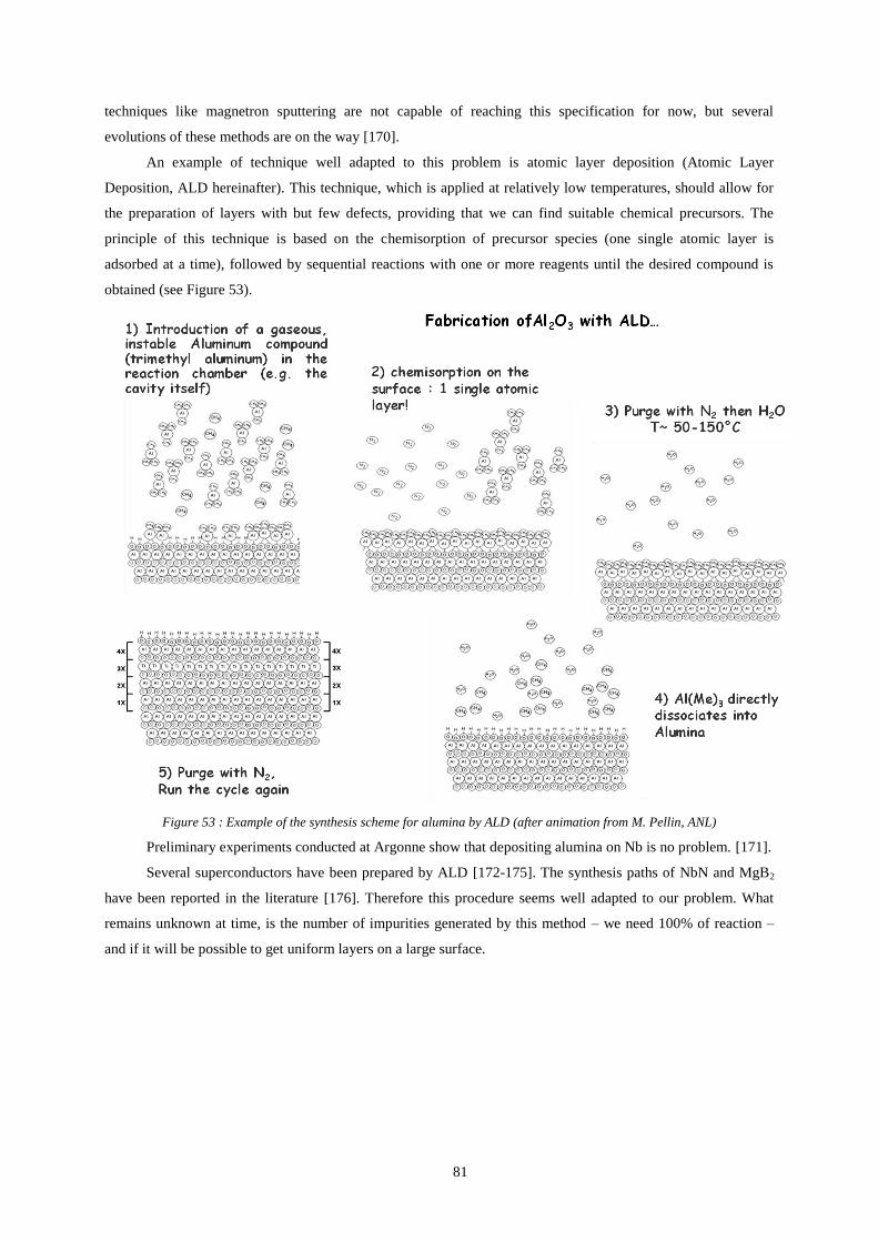
81
techniques like magnetron sputtering are not capable of reaching this specification for now, but several
evolutions of these methods are on the way [170].
An example of technique well adapted to this problem is atomic layer deposition (Atomic Layer
Deposition, ALD hereinafter). This technique, which is applied at relatively low temperatures, should allow for
the preparation of layers with but few defects, providing that we can find suitable chemical precursors. The
principle of this technique is based on the chemisorption of precursor species (one single atomic layer is
adsorbed at a time), followed by sequential reactions with one or more reagents until the desired compound is
obtained (see Figure 53).
Figure 53 : Example of the synthesis scheme for alumina by ALD (after animation from M. Pellin, ANL)
Preliminary experiments conducted at Argonne show that depositing alumina on Nb is no problem. [171].
Several superconductors have been prepared by ALD [172-175]. The synthesis paths of NbN and MgB2
have been reported in the literature [176]. Therefore this procedure seems well adapted to our problem. What
remains unknown at time, is the number of impurities generated by this method – we need 100% of reaction –
and if it will be possible to get uniform layers on a large surface.
82
6. Conclusion
The evolution of the SRF technology at the moment depends directly on problems related to the physics
of the superconducting materials. Advances in the technology are closely related to the understanding of
complex phenomena in superconductivity and in the physics of solids and surfaces. Accelerator physicists now
benefit a lot from collaboration with highly specialized communities in material, surface science and
superconductivity.
I hope to have shown that the dialogue between fundamental laboratories and development laboratories is
an effective way for arriving at an understanding of the limitations that we face, and finding novel and creative
ideas to overcome these. Such joint exploration is beneficial to both communities, because the practical problems
we need to solve often relate to innovative physics that as yet has been little explored.
Once the physics is understood, there is still a huge work ahead to translate this new knowledge into high
yield production of cavities for large SRF projects. This work is far behind the scope of this book, but occupies
most of the community. With a lot of efforts we have been able to carry Niobium close to its ultimate limits in
laboratories, but there is still large room for improvement for large scale production. I hope that understanding
better the origin and the balance of some of the limitations exposed here will help the reader to define tailored
specifications that are adjusted to his own application.
We also see that next generation SRF materials (thin films, multilayers) are about to emerge and that
strong R&D activity could lead to a breakthrough in this technology after several decennia of bulk Niobium
monopoly. I hope our community will seize this opportunity and will go on being dynamic and productive.
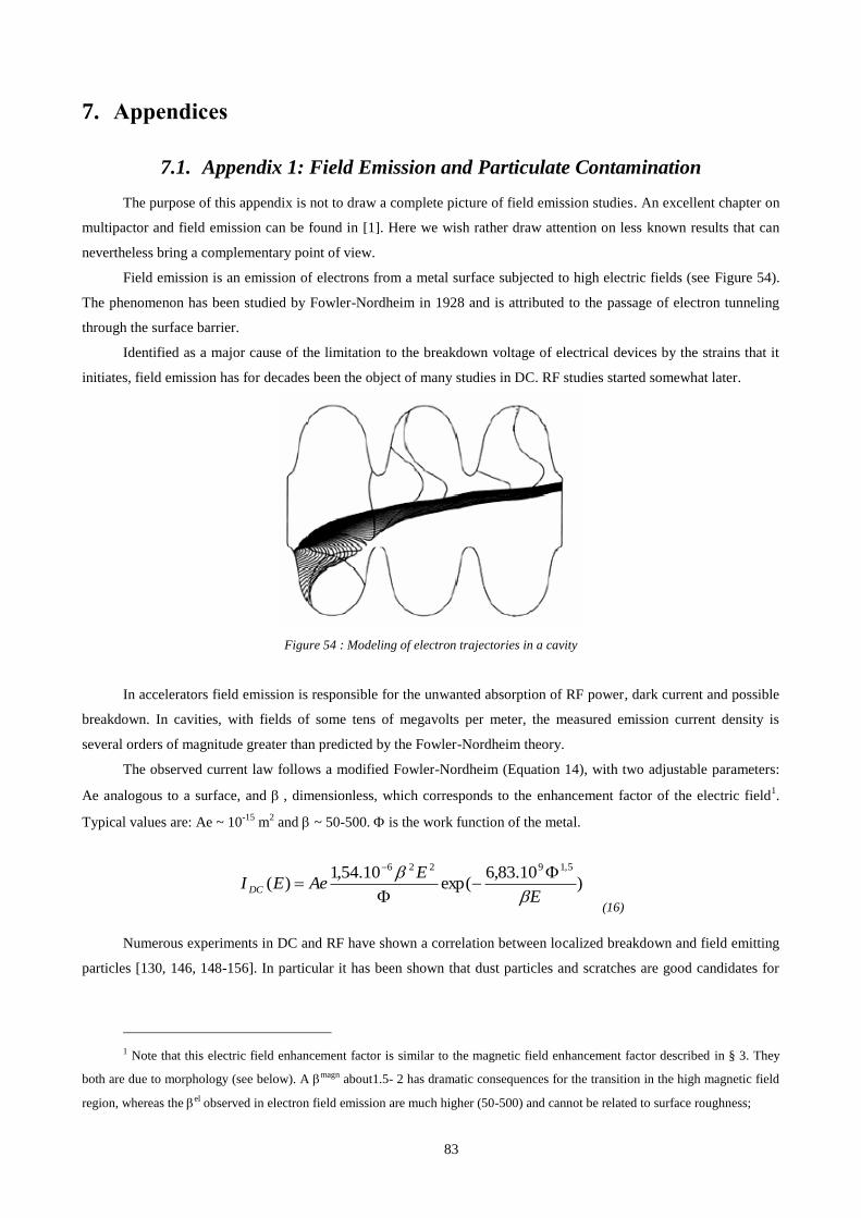
83
7. Appendices
7.1. Appendix 1: Field Emission and Particulate Contamination
The purpose of this appendix is not to draw a complete picture of field emission studies. An excellent chapter on
multipactor and field emission can be found in [1]. Here we wish rather draw attention on less known results that can
nevertheless bring a complementary point of view.
Field emission is an emission of electrons from a metal surface subjected to high electric fields (see Figure 54).
The phenomenon has been studied by Fowler-Nordheim in 1928 and is attributed to the passage of electron tunneling
through the surface barrier.
Identified as a major cause of the limitation to the breakdown voltage of electrical devices by the strains that it
initiates, field emission has for decades been the object of many studies in DC. RF studies started somewhat later.
Figure 54 : Modeling of electron trajectories in a cavity
In accelerators field emission is responsible for the unwanted absorption of RF power, dark current and possible
breakdown. In cavities, with fields of some tens of megavolts per meter, the measured emission current density is
several orders of magnitude greater than predicted by the Fowler-Nordheim theory.
The observed current law follows a modified Fowler-Nordheim (Equation 14), with two adjustable parameters:
Ae analogous to a surface, and , dimensionless, which corresponds to the enhancement factor of the electric field1.
Typical values are: Ae ~ 10-15
m2 and ~ 50-500. is the work function of the metal.
)10.83,6
exp(10.54,1
)(5,19226
E
EAeEI DC
(16)
Numerous experiments in DC and RF have shown a correlation between localized breakdown and field emitting
particles [130, 146, 148-156]. In particular it has been shown that dust particles and scratches are good candidates for
1 Note that this electric field enhancement factor is similar to the magnetic field enhancement factor described in § 3. They
both are due to morphology (see below). A magn about1.5- 2 has dramatic consequences for the transition in the high magnetic field
region, whereas the el observed in electron field emission are much higher (50-500) and cannot be related to surface roughness;
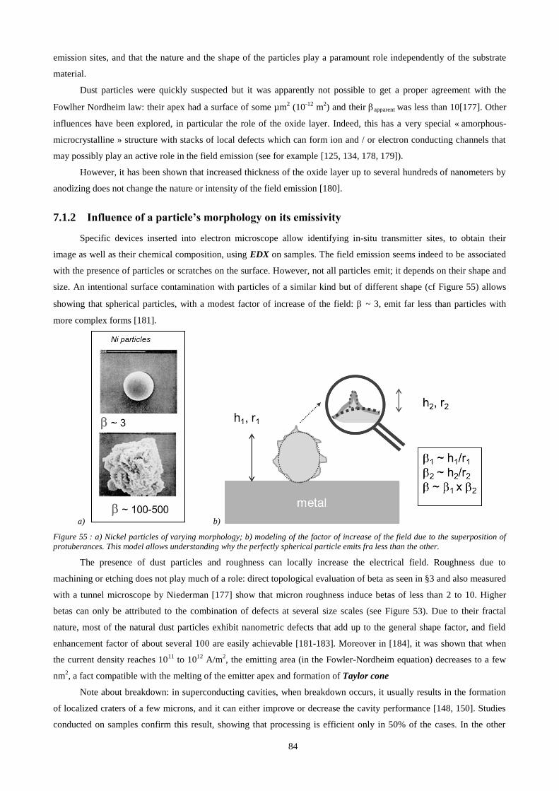
84
emission sites, and that the nature and the shape of the particles play a paramount role independently of the substrate
material.
Dust particles were quickly suspected but it was apparently not possible to get a proper agreement with the
Fowlher Nordheim law: their apex had a surface of some µm2 (10
-12 m
2) and their apparent was less than 10[177]. Other
influences have been explored, in particular the role of the oxide layer. Indeed, this has a very special « amorphous-
microcrystalline » structure with stacks of local defects which can form ion and / or electron conducting channels that
may possibly play an active role in the field emission (see for example [125, 134, 178, 179]).
However, it has been shown that increased thickness of the oxide layer up to several hundreds of nanometers by
anodizing does not change the nature or intensity of the field emission [180].
7.1.2 Influence of a particle’s morphology on its emissivity
Specific devices inserted into electron microscope allow identifying in-situ transmitter sites, to obtain their
image as well as their chemical composition, using EDX on samples. The field emission seems indeed to be associated
with the presence of particles or scratches on the surface. However, not all particles emit; it depends on their shape and
size. An intentional surface contamination with particles of a similar kind but of different shape (cf Figure 55) allows
showing that spherical particles, with a modest factor of increase of the field: ~ 3, emit far less than particles with
more complex forms [181].
a) b)
Figure 55 : a) Nickel particles of varying morphology; b) modeling of the factor of increase of the field due to the superposition of
protuberances. This model allows understanding why the perfectly spherical particle emits fra less than the other.
The presence of dust particles and roughness can locally increase the electrical field. Roughness due to
machining or etching does not play much of a role: direct topological evaluation of beta as seen in §3 and also measured
with a tunnel microscope by Niederman [177] show that micron roughness induce betas of less than 2 to 10. Higher
betas can only be attributed to the combination of defects at several size scales (see Figure 53). Due to their fractal
nature, most of the natural dust particles exhibit nanometric defects that add up to the general shape factor, and field
enhancement factor of about several 100 are easily achievable [181-183]. Moreover in [184], it was shown that when
the current density reaches 1011
to 1012
A/m2, the emitting area (in the Fowler-Nordheim equation) decreases to a few
nm2, a fact compatible with the melting of the emitter apex and formation of Taylor cone
Note about breakdown: in superconducting cavities, when breakdown occurs, it usually results in the formation
of localized craters of a few microns, and it can either improve or decrease the cavity performance [148, 150]. Studies
conducted on samples confirm this result, showing that processing is efficient only in 50% of the cases. In the other

85
50% of cases, breakdown results in a protruding particle welded on the surface which is a very stable emitting site, and
in a degradation of the cavity performance [130, 150]. With the improvement of cleaning techniques, surface fields up
to 80-90 MV.m-1
are currently observed without any breakdown or measurable field emission inside superconducting
cavities [161], whereas breakdown is a common feature in normal conducting cavities. The obvious difference between
superconducting and normal conducting cavities is the operating temperature; a thermally activated phenomenon like
electromigration being negligible at low temperature [185].
7.1.3 Analysis of the steps in the process of surface preparation
Quantifying the contamination occurring at various stages of surface preparation is a difficult task under the
operating conditions of a laboratory. The only means available exist in the microelectronics industry, are adapted at
« Wafers », and can be used only in a Cleanroom (CR). In collaboration with IBM Corbeil, however, we have been able
to study by difference the contamination brought about during each of the stages and identified some particularly
dangerous steps (for example, wet surfaces will re-contaminate easily under laminar flow whereas dry surface can be
exposed for a long time without getting polluted). In this way we have established that all rinsing and drying stages in a
CR were not or little contaminating. The early stages of the treatment, though, which took place outside a CR, gave rise
to a contamination that proved to be impossible to get rid of afterwards even after numerous low pressure rinsing.
Specifically, acid etching removed part of the contamination, but then re-deposited other types of particles [186-188].
7.1.4 Influence of assembly and vacuum handling
In the early 1990s, the dust created during cavity assembly was often cited as responsible for the field emission
phenomena observed during the testing of cavities, but there were no formal proofs. The incidents were listed in the
specifications of the experiments: leakage, problems during installation, change of seal, etc. Statistical study of
hundreds of tests stored at the laboratory and showed that the threshold for the appearance of electrons was about 4 to 5
MV.m-1
lower in case of a problem during assembly. This effect can only be shown statistically: indeed, only a small
portion of the surface may be at the origin of the emission, where the electric field is the strongest. The dust particles
accumulate in a random way and are not necessarily localized in the « danger zone ». Conversely, it will take but a
single dust particle in that particular zone in order for the electrons to be emitted. Our work has been able to confirm on
a substantial basis the intuitions that generally were held by the experimenters. It has led us to reconsider the role of
dust particles [189]. Vacuum handling also need some precautions : in [190], general operation like gasket assembly,
pre-pumping and venting, and steady state pumping have been monitored with a particle counter installed downstream
inside the vacuum system. It shows that any human operation, shock or strong vibration liberate a lot of particles. Only
steady-state pumping is rather benign in exception of startup or possible arcing. Any valve manipulation generates
particles if the pressure differential between both sides is high.
7.1.5 « post processing », a future solution?
We have seen in § 7.1.5 that assembly and jolts that necessary happen during transportation and installation of
cryomodules are liable to displace or create unwanted contamination. Wet processes in a cryomodule are excluded. One
approach that has been initiated in ORNL, FNAL or INFN is a plasma process. This cleaning technique is widespread in
many domains, but the originality of cavity treatment consists in the fact that one does not introduce an additional piece
in the cavity. The cavity is used already assembled in its final configuration and the plasma is triggered inside the cavity
at room temperature and moderate RF power thanks to its antennas and its own RF system [191]. Similar treatment has
been tried by putting an external magnet to obtain a cyclotronic resonance and ease the apparition of plasma [192].

86
Various type of plasma cleaning (low pressure helium, air plasma…) have also been tested at INFN Legnaro
[193].
Not only can we hope to destroy or at least « blunt » the field emitting particles, but we can also remove some
surface oxide and for example, subsequently rebuilt an oxide layer under dry oxygen. Dry grown oxide will hopefully
have fewer defects than the original oxide generated in wet conditions (see details in § 4.3). This « final » layer could
also help us fight against the very troublesome so-called “multipacting” effect in the accelerators. We know that the
layers of hydroxides on the surface after wet treatments applied to the cavities tend to increase secondary emission
coefficient and favor multipacting, and therefore a plasma treatment followed by re-oxidation could be beneficial at
many levels.

87
7.2. Appendix 2: Surface treatments.
This chapter summarizes the main features concerning the optimization of chemical and electrochemical
treatments of the cavity surface. However, these attempts are still done in an empirical way because we do not know the
exact link between surface states and SRF properties. For example, the effect of roughness was only recently
highlighted.
For optimization, multiple and sometimes antagonistic criteria have to be considered: cost and processing time,
ease of industrialization, safety issues, ease of rinsing, contamination with hydrogen… and reproducibility.
For many years chemical polishing was used, the most common mixture being a mixture of fluoric acid HF (1
volume), nitric acid HNO3 (1 volume) and orthophosphoric acid H3PO4 (2 to 4 volumes) which act like a buffer to slow
down the reaction. The term “polishing” is not correct: it rather is an “etching”, since grains are attacked at different
rates and crystal defects such as grain boundary or the emergence of dislocations tend to be revealed by the treatment. It
is, however, a treatment that is fairly easy to implement. In its most current form, the etching rate is about 1 µm/min,
thereby removing large thicknesses fast enough, while not being too much bothered by the time needed for filling and
emptying large cavities: the thickness removed remains under control. This treatment is highly reproducible but leaves
rough surfaces.
On the contrary, electropolishing produces much smoother surfaces, and has proven to produce record
accelerating gradients and is now widely used for cavities. The most common used mixture is HF (1 volume) and
sulfuric acid H2SO4 (9 volumes). Unfortunately the results are much more dispersed. For large accelerator projects it is
essential to understand the origin of these dispersions and to improve the process, especially because it is relatively
expensive and dangerous.
Figure 56 shows schematically the difference between BCP and EP. In both case the polishing occurs by
successive oxidation and dissolution of the oxide in HF. In the case of chemical polishing the oxidation occurs because
of the presence of a strong oxidant in the solution: NO3-, while in electropolishing the oxidation occurs because of the
bias applied to the anode. Because of the presence of water, the stable form of Nb is Nb2O5. But HF discomposes the
oxides into NbF5 which is soluble into the solution.
Here we focus primarily on work done on electropolishing, which by now has replaced the chemical treatments.
For more details on these, see [105, 116, 117, 194-197]
Electropolishing is a technique widely applied in industry for brightening purpose. In this case it is used in very
different conditions from the one used for Niobium polishing: usually brightening needs short processing time and the
cathode surface is very large compared to the parts to be treated (anode), so the current density is not too much affected
by the geometry of the anode . In these conditions, it has been extensively studied although it is a very complex process
[170, 181].
There are several electropolishing (EP) processes applicable to Niobium [198], but the most efficient one was
developed by Siemens in the 70’s [199], in a mixture of sulfuric and hydrofluoric acids. Application to large cavities
has been done at KEK during the 80’s where a thorough work has been completed taking many practical aspects into
account [200]. After the effect of baking revealed the advantage of EP, many other laboratories are now involved in
related R&D.

88
Figure 56: comparison between chemical polishing (left) and electropolishing (right). In both case Niobium is oxidized into Nb5+ In
the case of chemical polishing the oxidation occurs because of the presence of a strong oxidant in the solution: NO3-, while in
electropolishing the oxidation occurs because of the bias applied to the anode. Because of the presence of water, the stable form of
Nb is Nb2O5. But HF decomposes the oxides into NbF5 which is soluble into the solution.
7.2.2 Electropolishing basics
Several current-voltage behaviors can be expected for a metal inside an electrolyte solution (cf Figure 57),
among them, the most common are active dissolution (similar to chemical etching), or passivation (e.g. Nb or Al in pure
water). Electropolishing refers to a phenomenon where a current plateau (about 50-100 mA/cm2) appears, usually
attributed to a diffusion limited phenomena. Polishing and brightening effects are attributed to the existence of a highly
resistive viscous layer [201-205]. When proper electropolishing conditions are established, nearly all voltage drop
occurs in this viscous layer and the polishing process is not much influenced by ohmic losses in the solution. This
translates into the existence of a large plateau where polishing is effective independently of the cathode anode distance.
Unfortunately this condition is seldom achieved in cavities because of unfavorable parameters: high agitation due to
rotating set-ups, small ratio between cathode and anode area, long treatment time leading to temperature increase,
enhanced HF evaporation and premature aging of the polishing solution.
Figure 57: Schematic current voltage curves in various typical situations: active dissolution, when no viscous layer is formed and the
metallic ions dissolve freely in electrolyte; passivation, where formation of a stable, insoluble film prevents further corrosion, and
electropolishing, where an interface layer (viscous layer) is a source of limitation in current. In the absence of reference electrode, V
figures Vanode-Vcathode and includes ohmic losses inside solution.
Nb5+
Nb0
e-
e-
2H+ + 2e-
H2
NbF5
Nb5+
NbF5
NO3-
Nb0
e-
Nb5+
6 Nb + 10 HNO3 3 Nb2O5 + 10 NO + 5 H2O
Nb2O5 + 10 HF 2 NbF5 + 5 H2O
Nb Nb5+ + 5 e- Nb2O5
Nb2O5 + 10 HF 2 NbF5 + 5 H2O

89
For instance in an horizontal EP set-up, the slope of the I(V) curve increases with rotation speed [206].A
classical electropolishing I(V) curve shows a characteristic plateau where the current is limited on a wide range of
potential. Polishing is a combination of macro- and micro-polishing. Wagner made a theoretical prediction of the rate of
leveling of microprofiles at the limiting current, based on a diffusion layer [202, 207, 208]. Choosing the voltage at the
highest cell impedance V/I is a criteria that allows optimizing the macrolevelling and this criteria is widely used in
practical applications [209, 210]. This point is situated on the current plateau of the I(V) curve (Figure 57). This theory
applies to anodic leveling (roughness rms ~ 1µm) and not to anodic brightening (rms << 1µm). The apparition of the
plateau depends a lot on the field distribution in the “electrochemical cell”. Its presence in a simple sample set-up with a
moderate stirring does not guaranty its presence in a cavity with a more complex geometry and a lot of stirring due to
the movement of the cavity, hydrogen bubbling or circulation of the solution for cooling purpose. In particular, the
reduction of the cathode/anode ratio can lead to its disappearance [211].
In our case a phenomenon of current oscillations is superimposed on the classical curve (see Figure 58).
Figure 58 : curve I(V) of Niobium in the EP solution (1 vol. HF-9 vol H2SO4)
Note that the original process developed by Siemens for Nb, is based on the oscillations that appear at the end of
the plateau, and the absence of stirring. The topic is controversial: some authors claim that oscillations are mandatory to
gain very good surface states, in particular in the case without any stirring [199, 212, 213]. Good surface state has also
been achieved in voltage and temperature conditions where no oscillation was observed [200]. Oscillations could issue
from the growth/dissolution of a porous external oxide layer [214, 215].
Microleveling is only possible under transport control, which is the case in the current plateau. In this case 3
possibilities occur; either the process is limited by the diffusion of the metal ion from the anode to the bulk of the
solution, or it is limited by de diffusion of the anion (in our case F-) or by diffusion of H2O to the anode.
Figure 59: Diffusion scenarios for microleveling during EP. I) the process is limited by the diffusion of the metal ion (Nb5+) from the
anode to the bulk of the solution. II) Reaction limited by the diffusion of anion (in our case F-) III) Reaction limited by the diffusion of
H2O to the anode. figures the diffusion layer thickness and CS is the saturation concentration of each species (after[216]).
Volts
I (A)
1
5 10 15
0
Volts
I (A)
1
5 10 15
0
I) Metal Ions (Mn+aq) II) Acceptor anion (A) III) H2O
Distance from electrode
Co
nce
ntr
ati
on
H2O
A-
Mn+aq
Cs
H2O
A-
Mn+aq
Cs
H2O
A-
Mn+aq
Cs

90
Depending on the limiting species one can determine how to modify the solution composition to optimize the
process. Electrochemical Impedance Spectroscopy and voltamperometric measurement allow determining that
electropolishing of Nb in a HF/H2SO4 mixture is limited by F- diffusion [217, 218]. We will see here below, that the
content of HF of the solution plays a paramount role in the success of EP.
7.2.3 Aging of the EP solution, corrosion of the electrode and sulfur particles
The origin of the production of sulfur particles in the system of electropolishing has been investigated [219-222].
This results from a phenomenon of corrosion of the aluminum cathode (simultaneous oxidation of aluminum and
reduction of sulfates). Aluminum is passive in the EP solution because of the forming of an ammonium fluoride that is
insoluble in the sulfuric acid. We cannot prevent this reduction of sulfuric acid, but it remains at a very low level as
long as there enough fluoride in the mixture. With the aging of the bath, the amount of HF tends to decrease
(consumption through the reaction with the Niobium, evaporation) and the sulfur particles appear in the vicinity of the
cathode. Higher voltage seems to promote indirectly sulfur generation: because of the higher current density,
temperature tends to increase and higher temperature favors HF evaporation and faster aging of the EP solution [223].
In some conditions that still need to be clarified, Niobium oxide particles are also observed (see e.g. [224]). All these
particles, initially suspended in the solution, deposit slowly on the walls of the system, including the cavity. These
particles are suspected to cause the increased field emission observed on electropolished cavities. We do not know the
precise form of this sulfur, but unlike classical dust particles, the particles adhere to the surface and are but poorly
cleaned by high pressure rinsing. IR spectra of some of the particles show the presence of organic molecules, probably
due to the action of sulfuric acid on the polymers with which it is in contact [223]. The particles are insoluble in water,
but not in chlorinated solvents and ethanol [219]. Washing with ethanol is now routinely applied for the production of
cavities at DESY and seems to prove its use. Other alternative treatments are under study: ultrasonic degreasing, light
chemical polishing, peroxide rinsing…
The aging of the bath seems to be also one of the keys to the effectiveness of the treatment. With time the
etching rate decreases, and the bath is usually changed when concentration of Nb reaches 10g/l. Under certain
conditions brightening ceases to be effective for smaller quantities of Niobium dissolved. Time required to reach
maximum brightness and the amount of Niobium dissolved depend critically on the amount of F- in the solution.
Very dilute solutions do not improve the roughness [225], but could be a way to remove thick layers before a
final, lighter, electropolishing. Addition of water in small amounts degrades the brightening, probably because it favors
the formation of insoluble oxide. This aspect probably is involved in the aging: because the concentrated sulfuric
solutions are very hygroscopic and over time they tend to absorb moisture from the air.
Low voltage EP allows reducing temperature escalation and reduces HF evaporation. It is more favorable in term
of sulfur particles production and is not detrimental to cavity performances [223].
7.2.4 Field repartition, modeling
On nearly all EP facilities it is observed that polishing is quite different between iris and equator, which is the
sign that we do not achieve a perfect viscous layer in our conditions. One of the symptoms of this situation is that there
is no or small plateau in the I(V) curve. Because of ohmic losses in the EP solution the voltage close to the cavity wall
is different at equators compared to irises. In case of the plateau the same current (i.e. etching rate) is observed for a
large range of voltage whereas when the I(V) curve presents a slope, the etching rate is higher at higher voltage, that is,
close to the irises. For long etching treatment the difference can amount to 100eds of µm. Care has to be taken that the
removal rate is more or less the same (by checking the field distribution for example, see [226]). One way to overcome
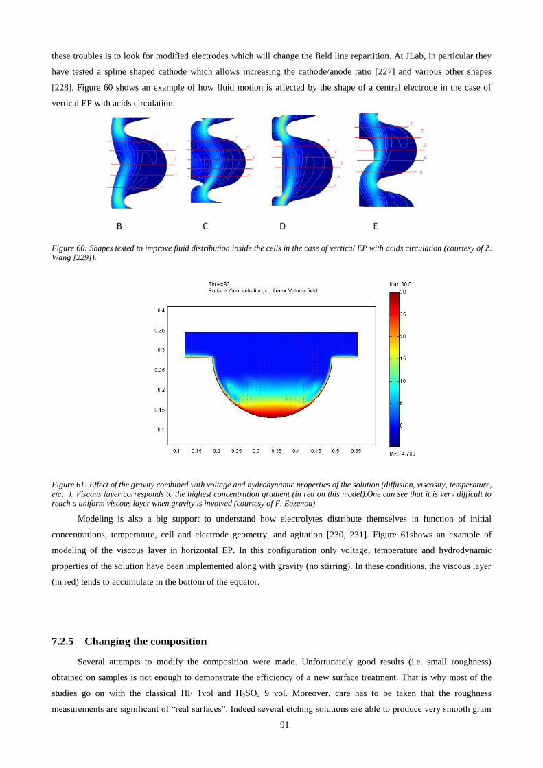
91
these troubles is to look for modified electrodes which will change the field line repartition. At JLab, in particular they
have tested a spline shaped cathode which allows increasing the cathode/anode ratio [227] and various other shapes
[228]. Figure 60 shows an example of how fluid motion is affected by the shape of a central electrode in the case of
vertical EP with acids circulation.
Figure 60: Shapes tested to improve fluid distribution inside the cells in the case of vertical EP with acids circulation (courtesy of Z.
Wang [229]).
Figure 61: Effect of the gravity combined with voltage and hydrodynamic properties of the solution (diffusion, viscosity, temperature,
etc…). Viscous layer corresponds to the highest concentration gradient (in red on this model).One can see that it is very difficult to
reach a uniform viscous layer when gravity is involved (courtesy of F. Eozenou).
Modeling is also a big support to understand how electrolytes distribute themselves in function of initial
concentrations, temperature, cell and electrode geometry, and agitation [230, 231]. Figure 61shows an example of
modeling of the viscous layer in horizontal EP. In this configuration only voltage, temperature and hydrodynamic
properties of the solution have been implemented along with gravity (no stirring). In these conditions, the viscous layer
(in red) tends to accumulate in the bottom of the equator.
7.2.5 Changing the composition
Several attempts to modify the composition were made. Unfortunately good results (i.e. small roughness)
obtained on samples is not enough to demonstrate the efficiency of a new surface treatment. That is why most of the
studies go on with the classical HF 1vol and H2SO4 9 vol. Moreover, care has to be taken that the roughness
measurements are significant of “real surfaces”. Indeed several etching solutions are able to produce very smooth grain

92
surface, while defects like grain boundaries exhibit huge steps. Techniques like AFM are not able to measure
adequately such surface feature, if not properly calibrated.
Among the variation of composition tested one can cite BEP tested at JLab (a mixture of lactic, sulfuric, and
hydrofluoric acids; BEP stands for buffered electropolishing). This treatment provides very bright and smooth surfaces
with a larger etching rate, but is not diffusion limited (no plateau). It needs the development of specific electrodes [232].
Sulfuric-methanol mixtures are widely used in electropolishing and has been applied to Niobium [233].
Another interesting approach is ionic liquids like i.e. Choline chloride (C5H14ClNO) based mixture containing
ammonium or urea [234] or another recipe as studied in [235]: 2-hydroxyethyl-trimethylammonium chloride, ethylene
glycol, urea and ammonium fluoride. Ionic liquid are very interesting from the safety point of view but any change of
the composition will require a full development that might take some years.
In conclusion classical EP will likely be a mandatory step for a long while although aging of polishing solutions
is problematic. Good results have been obtained by adding a final short etching (either EP or BCP) with fresh acids after
a heavy EP. Reducing the necessary EP is to our opinion the best way to mitigate aging and reproducibility problems.
The combination of the new barrel polishing techniques producing very low damaged layer with shorter EP is an
interesting road for the future.

93
7.3. Appendix 3: Nb machining/Forming1
As stated before, pure Niobium is very soft and acts like soft copper or lead. Detailed information on the
mechanical properties, machining techniques, etc. can be found on websites of suppliers. Nevertheless, information on
the websites holds true only for Niobium alloys such as NbTi, or commercial Nb. High purity Nb is discussed below.
7.3.2 Forming
In the case of high pressure forming processes such as spinning, heavy deep drawing, Niobium has a tendency to
stick to the tools and thus special lubricants and die materials are required: brass, bronze; (Be-Cu or steel have also been
used). In the case of forming processes involving smaller deformations, such as half-cell deep drawing or hydroforming,
aluminum tools are commonly used without the sticking problem.
7.3.3 Machining:
Niobium has a tendency to gall or to seize to tooling and this requires the use of tools with specific angles and
proper lubrication. Tools must be very sharp and run at high speeds and steel tools work better than carbide tools.
Manual feed (rate at operator’s discretion) helps in rapid removal of Niobium chips. While working with high RRR
material, the speeds must be increased by a large factor compared to ones found in the literature, (cutting speed ~ 250 –
270 rpm for steel and 350 – 400 rpm for carbon tools.
7.3.4 Lubricant: discussion
The choice of a proper lubricant and its interaction with Niobium surface has been a major topic of discussion.
Nevertheless one cannot avoid surface contamination and cold working upon any type of forming of Niobium. Priority
should be given in accordance to the ensuing cleaning procedure.
Therefore silicon type oil must be avoided, as it is very difficult to eliminate. Light hydrocarbon molecules that
can be effectively rinsed/degreased are preferable (e.g. ethanol, water soluble hydrocarbon…).
As particle contamination is also an issue in SRF application, lubricants with particle suspension like graphite or
MoS2 should be generally avoided, although appropriate cleaning procedure helps overcome this problem.
Any organic lubricant reacts with freshly cut Nb surface, but it results only in surface contamination that will be
eliminated by subsequent chemical etching.
7.3.5 Recommendations
• Need for high thermal conductivity:
- High RRR material
• Sheet material (forming)
- Recrystallized material (800° C, 2 h)
- Uniform grains without different local grain size
- Small grain size (ASTM 5 or finer)
- Yield strength should be 50 MPa < 0.2 < 80 MPa.
1 Most of the information found here has been published at FNAL as TD-06-049.

94
With such conditions, we can achieve a fairly high strain hardening coefficient (n> 0.3), and a more uniform
distribution of deformation in the material. These conditions do not affect purity and RF properties, but are very helpful
to any forming process.
• Rod (drilling, machining)
– Lubricant must be easily removable (no SILICONE grease !!!)
– Recrystallization is not mandatory prior to working (unless the material has already been subjected to
extensive cold working)
– Recrystallization is mandatory AFTER machining!
– Small grain material is better (because of differential etching rate)
For low RRR material, it is also worthwhile to have a well recrystallized material. Meanwhile the hardness,
tensile strength and yield strength will be a little higher than for high RRR. Typical values for material with RRR of 30
are: 0.2 ~ 230-250 Mpa, max ~ 280-300 MPa, Hv ~ 60-70. This also means forming is more difficult compared to high
RRR material.

95
7.4. Appendix 4 : Hydroforming
Here again we will not give a complete picture but only expose the general philosophy and, as an example, show
partial results obtained at Saclay in the 90’s.
As we have already mentioned several times, the control of welds is a sensitive stage in the production of
cavities on an industrial scale. Hydroforming of Niobium tubes provides a fabrication scheme allow avoiding equator
and iris welds. This technique can be applied at room temperature and avoids heating the Niobium. There have been
several attempts to hydroform Niobium in our community: at Cornell and CERN in the 80’s [236, 237], at Saclay and
DESY in the 90’s [238, 239]. Up today, DESY is the only lab that had a continuous and complete program (see [101,
240] and reference therein).
The main problem in hydroforming is the supply of tubes with correct metallurgical properties that stand
elongations up to 200% (to be compared with deformations about 30 % applied to sheets to form half cells).
It requires tubes with especially small grains and specific texture which are usually not commercially available
and need the development of a specific fabrication scheme. Developing new metallurgical fabrication scheme is very
expansive and is at the origin of the lack of spreading of this technique.
The success of the various isolated attempts shows that the technique is nevertheless feasible and that no strong
technical obstacle exists.
The choice at Saclay was to start from a tube of a diameter intermediate between the iris and the equator, to
hydroform at the level of the equator and then spin at the level of the iris.
Even so, to pass from a tube to the finished cavity, we need elongations of over 200%, while current (uniform!)
elongations are in the order of 30-40%. We must therefore consider various deformation/restoration cycles, hence the
importance of previous studies on recrystallization. It is also clear that the metallurgical quality of the original tube is
essential for the success of such a project.
Also the deformation cycle must be studied carefully to optimize the deformation path and stay far from the
rupture. It has been modeled by finite elements for Niobium and for copper, as copper cavities were used in certain
applications where the Niobium is deposited in thin layers.
Finally, in the context of an industrial transfer we built a hydroforming press at an industrial site (Bourgogne
Hydro), allowing us to conduct all our testing and successfully produce several cavities in copper and Niobium.
7.4.2 Manufacture of the tubes
After the failed attempts starting with rolled, welded and hammered sheets, we had to make a tube by extrusion
of a billet and flow-forming the section of the tube thus obtained.
On paper the task looked relatively easy: produce a tube with a strain rate large enough for recrystallization to
result in very small equiaxed grains. But once again the development for the pure material proved very difficult. (At the
first extrusion attempt, the Niobium - RRR ~ 200 - got completely stuck to the tools and blocked the press: we had to
re-make the bronze tools to have the best tribology properties.)
Our first tubes had a grain size that was relatively uniform (80-120 µm) but still exhibited a « roped » texture
that turned out to be harmful. The ruptures were however sufficiently close to the final form to give us hope (Figure 62).

96
a) b)
Figure 62 : a) First Niobium tubes obtained after the development of a manufacturing range especially adapted at Niobium of high
purity; the tube is pushed back and slightly machined to ensure uniform thickness of the final piece. b) Micrography of a tube
showing a uniform grain size (80-120µm).
Because of budgetary problems we continued with Niobium of lesser quality, which then was post-purified.
The tubes of OHFC copper are available commercially and several cavities were successfully hydroformed..
7.4.3 Modeling
The modeling was done using software for finite elements (Forge 2, developed by the Ecole des mines). The
material’s rheology is estimated from the traction and adjusted using a simple law: Hollomon’s: = K n where K is a
« consistency » term and n the famous strain hardening coefficient already mentioned. is the strain and is the stress.
It is assumed that the metal is isotropic and follows a simple criterion of von Mises expressed on the principal
axes according to the Equation (15):
√ [
] ̅ (17)
where is the equivalent stress. The curve )pH.(
-
is extrapolated from the actual stress-strain curve
where pdp
-
. In the case of Niobium the calculation is also coupled with a Coulomb type friction law.
Taking into account all these assumptions, the forming limit follows the law (16):
n1
2
1n
2+-1n2nK
(18)
where :
K is the consistency, n the strain hardening coefficient, the ratio of principal stresses (, z semi-polar
coordinates):
z
In the light of this criterion we can extrapolate a path in the stress space which allows to hydroform a tube
without tearing or folds. The initial ratio between the internal pressure and the displacement of the tools proved
essential to secure a quasi-spherical form. However, this criterion considers only the material’s rheology. It allows good
predictions of the deformation but does not foresee the appearance of the necking. We have added a criterion that
permits to predict the rupture. We were able to show that von Mises criterion (commonly used in forming) is applicable
in our case [238].

97
a)
b)
Figure 63 : a) Example of modeling by Forge 2, b) Results of the first hydroformed cavity. Compared to the performance at the time,
the 18 MV / m are quite decent for Niobium of commercial quality.
Following this work, we have realized a hydroforming tool that allowed us to form several mono-cells in
Niobium and in copper. Figure 63a shows the modeling that was applied to find out the deformation sequence, while in
b) one can see a picture of a cavity made out commercial Nb and post annealed and its performances (test realized in
1998).

98

99
8. Glossary and acronyms
ALD: Atomic Layer Deposition, technique for depositing films, atomic layer by atomic layer, by using various
precursor chemicals. These films are homogeneous and perfectly fit the surfaces, even the most complex ones.
AFM: Atomic Force Microscopy
ARXPS (or ARPES): Angle resolved X-Ray Photoelectron Spectroscopy (see XPS), By varying the incident or
detection angles one detects electrons coming from different depths and get a probe of the depth distribution of the
considered species.
BCP: “buffered chemical polishing”
BCS: “BCS theory (Bardeen-Cooper-Schrieffer) is the microscopic theory that describes superconductivity. It
can be used to describe the surface resistance of a superconductor in RF field. The residual resistance gathers additional
contributions to surface resistance which origin is less determined.
Cleanroom: particulate controlled environment room, as used in microelectronics
Cold work: see strain hardening or damaged layer
CTR (Crystal Truncation Rod): or “method of the truncated crystal”. The fact that a crystal is not infinite but has
a surface has consequences for the shape of the diffraction peaks. If moreover movement of atoms or the surface is
reconstructed, this induces particular structures between the Bragg peaks. These phenomena are of a very weak
intensity and can only be observed with sufficiently intense light sources (synchrotron).
Cultural noise: Cultural noise consists in all the vibrations generated by human activity: pumping, traffic, noise
in general, even if the sources are distant. Accelerators provide a very sensitive means to measure such things: for
example, the LEP at CERN was sensitive to the effects of the earth tides or the passage of the TGV Paris Geneva
Cyclotronic resonance: condition under which the combination of an RF field and a magnetic field leads to very
special electron trajectories. This resonance is in particular used to trigger plasmas in gaseous media with a low energy
input.
Damaged (surface) layer: layer that is strongly deformed by the contact with equipment during a forming
process. This operation results in deformed and textured grains, and a significant increase of the dislocation density
(residual stresses) inside the material. A recovery annealing or recrystallization can remove the residual stress, lower the
dislocation density, and in the case of recrystallization induce new grain boundaries.
Diffuse scattering: X-ray diffraction technique where one places the detector offset from the main beam.
Diffuse scattering is a primary x-ray beam scattering on the crystal lattice defects. It is observed as an elevated
background in the vicinity of Braggs peaks. We can thus detect very weak signals due to lattice distortion.
Dislocations: crystalline defect similar to a half-crystalline plane inserted between two completed crystalline
planes (edge) or connected to the half plane one atomic layer below (screw). In practice a dislocation can be any
combination of a screw and an edge dislocation. It is a linear type of defect, compared to point defects (vacancies or
interstitial atoms) or 2D defects like surfaces and interfaces (between grains or phases).
EBSP or EBSD: Electron Back Scattering Pattern (or Diffraction) or Kikuchi pattern: diffraction pattern that
depends on the crystal orientation, which also allows to quantify the degree of misorientation due to crystalline defects.
EDX (Energy Dispersive Xray analysis): method of elemental analysis by XRF of atoms, often installed on
electron microscopes.
Emittance: A parameter proper to an accelerated beam that describes both the cross section of a beam and its
tendency to diverge from it. The emittance should be as low as possible to avoid losses.
Elastic Limit : See Yield Stregth.

100
EP: « electropolishing»
Equiaxial (grains, crystal structure): crystal structure where the grains have an axisymmetric form, the grains
are neither elongated nor flattened.
ERDA: Elastic Recoil Detection Analysis, also called HFS (Hydrogen Forward Scattering).
Getter: materials very reactive with light elements, which are used for purifications under moderate conditions
of temperature and vacuum. The best known example is titanium, used in the sublimation pumps. In our case it is used
as a thin layer on the Niobium where it reacts preferentially with the oxygen that diffuses to the surface during thermal
treatment.
GDS: Glow Discharge Spectroscopy Elemental analysis method.
HFS: Hydrogen Forward Scattering. See ERDA
HOM: “high order modes”, higher harmonics of the resonance mode of a cavity
HPR: High Pressure Rinsing
HRCLS: High Resolution Core Level Spectroscopy. Variation of XPS. Spectroscopy at the levels of hearts. By
using a synchrotron radiation source, with different angles of detection and / or several energies of incident radiation,
one achieves better energy resolution and greater accuracy on the results. Indeed, they are more reliable because the fits
have to « work » for several spectra simultaneously.
Hydroforming : method of shaping materials particularly well suited for shaping tubes. This method uses both
the pressure of a fluid and the displacement of tools.
ILC: International Linear Collider: international project for the future e+/e- collider for particle physics, aiming
at 0.5 TeV in the center of mass, and successor to the LHC. The project is based on the developments made in the
collaboration TESLA.
IR: Infrared Spectrometry
Josephson junction: Junction composed of two superconductors spaced by an insulating layer of a few nm. If
the insulating layer is thin enough, there is a coupling between the two superconducting layers: Cooper pairs can pass
from one to another in a quantified manner.
Kapitza (resistance): thermal resistance at the interface between two different environments which reflects the
efficiency of heat transfer. This resistance, which must be as low as possible, plays an important role in the thermal
stability of a cavity.
Klystron: Klystrons are used as amplifiers at microwave and radio frequencies to be used as RF power supply
for cavities. For more detail see http://en.wikipedia.org/wiki/Klystron .
Linac: linear accelerator
Maximum elongation: in a tensile test : elongation of material reached when the material breaks. Although this
data is widely used, it is not relevant for forming behavior: uniform elongation should not be exceeded.
MBE (Molecular Beam Epitaxy): The MBE is a technique that involves sending one or more molecular beams
to a substrate adequate for epitaxial growth, i.e. with a crystal lattice close to the film to be deposited.
Micro-porosities: metallurgical term designating the micro-bubbles or blisters formed by diffusion of light
elements in the still liquid phase during the solidification of Niobium. These bubbles are then « packed » during
operations of forging and rolling, and appear as small irregular craters revealed by chemical treatment.
Multipacting: phenomenon of an avalanche of electron emissions. If the secondary emission coefficient of the
surface is very high, it may happen that the impact of an electron in the wall generates a cascade of secondary electrons,
and if resonance conditions are met, this will amplify itself. This phenomenon can generally be overcome through a
conditioning from a few hours to several days, but it would of course be more economical if one could avoid it.

101
Necking: When a material reaches the Ultimate Tensile strength the deformation cease to be uniform and
concentrates locally leading to eventual failure.
Oxipolishing: polishing method which consists in growing an Niobium oxide by anodization and then dissolve it
in a solution of hydrofluoric acid. The operation, which must be repeated several times to remove thick layers, is very
well suited for the removal of thin layers.
Passive metal: Metal forming an oxide insulator, and chemically very inert
Passive, passivity: see Passive Metal.
Peierls Transition: structural alteration that appears at low temperature and puts a metal or semiconductor in the
insulating state.
PIXE: Proton Induced X-ray Emission
Poisson ration (dimensionless). When a material is compressed in one direction, it usually tends to expand in
the other two directions perpendicular to the direction of compression. This phenomenon is called the Poisson effect.
Poisson's ratio is the ratio of the (elastic) normal strain in a transverse direction (after a change of sign) to the normal
strain in the direction of loading under an applied normal stress.
Proximity effect: because of their coherence length (several tens of nm), the Cooper pairs of a superconductor
may subsist within a metal in direct contact with it, inducing a kind of « superconductor » behavior in the metal. This
effect is of course highly dependent on thickness and the quality of the interface between metal and superconductor.
Quench: generalized transition phenomenon of the cavity from the superconducting to the normal state. The
conditions for resonance of the cavity change and nearly all power is reflected. The same term is used to designate fast
cooling processes (for steel after forging… or cavity cooldown).
Recovering: annealing process that can remove the residual stress (strain hardening) in a material. Depending on
the temperature or duration, recovering can happen in the same time as recrystallization or below. During recovering the
density of dislocation is reduced.
RF: « radiofrequencies », electromagnetic field at frequencies between some tens of MHz and some GHz.
RRR: « Residual Resistivity Ratio »
Segregation: local concentration of impurities (usually interstitial atoms) in a crystal lattice.
SIMS: Secondary Ions Mass Spectroscopy. Elemental analysis method.
SRF: « radiofrequency superconductivity », the domain of the application of RF electromagnetic field to
superconductivity, mainly the cavities and the systems for accelerators.
STM: Scanning Tunneling Microscopy.
Strain hardening: increase of dislocation density in a material due to deformation. Cold work hardens the
material and renders the forming difficult. Intermediate recovering annealing might become necessary.
Synchrotron: a circular electron accelerator used for generation of electromagnetic radiation in the frequency
ranged over terahertz.
Taylor cone: Conducting liquids subjected to fields (either electric or magnetic) tend to form cone-shaped
structures (Taylor cones) oriented along the field lines, and stabilized by the balance of electrostatic and surface
tensions forces.
TEM: “Transmission Electron Microscope”.
Texture: Preferred orientation of grains (microcrystallites) of material, often specific to a type of lattice and
strain method used.
Tumbling: mechanical polishing process where “granules” of various sizes and nature are introduced inside the
cavities. Abrasion is achieved through more or less complex ways of rotation. Also called centrifugal barrel polishing.

102
Twinning: crystalline transformation where atoms from a crystallite rearrange themselves on both side of a
common symmetry plane, each side becoming mirror like of the other. This transformation is irreversible, but its
mechanism is different from a plastic deformation. In principle it appears rather at low temperature, and the movement
of atoms necessary to induce it is in the range of one atomic distance.
Type I/ type II superconductors: Type I superconductors like lead (Pb) exhibit only one transition (at HC) from
the Meissner state to the normal conducting state. In the Meissner state, if an external screening current appear at the
surface of the superconductor (in the penetration depth ) and produce a magnetic moment opposite to the external
field. all magnetic fields up to HC. Type II superconductors like Niobium are also in the Meissner state up to their first
critical field HC1. HC1 corresponds to the transition of the purely superconducting state to a mixed state, where both
normal and superconducting areas coexist. The second critical field HC2 corresponds to the transition from the mixed
state to the normal state. HC is the critical thermodynamic field.
Ultimate Tensile strength: is the maximum stress that a material can withstand while being stretched or pulled
before necking, which is when the deformation cease to be uniform and concentrates locally.
Uniform elongation: in a tensile test: maximum elongation of the material where the deformation keeps uniform
(before necking). It is the elongation to be considered for forming, rather than the maximum elongation.
Valve metal: Metal oxide which forms a highly insulating oxide (passive) when polarized anodically and easily
corrodible when polarized cathodically. These are usually metals with higher oxidation states (Al, W, Ti, Ta, Hf, Nb,
Zr).
Wakefield : Field induced by a particle that passes through a vacuum chamber, due to the interaction with the
walls. It produces short-range interference effects (interaction with the particles of the same « package»), as well as
long-range effects (next packages).
XFEL: « X Free Electron Laser », European project for a free electron laser decided upon late 2007. It will
require ~ 800 cavities 9-cells 1.3 GHz.
XPS: X-Ray Photoelectron Spectroscopy, also called ESCA. (Electron Spectroscopy for Chemical Analysis). X
rays eject core electron from a specific atom. The kinetic energy of this electron depends on its binding energy which is
slightly influenced by its chemical state and close neighbor atoms. This techniques is very superficial (3-10 nm in
depth) and not very sensitive (typically 0.5 At %), but it is one of the few that provides chemical information in addition
to elemental analysis.
Yield Strength or Elastic Limit: is defined as the stress at which a material begins to deform plastically. Prior
to the yield point the material will deform elastically and will return to its original shape when the applied stress is
removed. Once the yield point is passed, some fraction of the deformation will be permanent and non-reversible. In
practice, it is measured when 0.2% of deformation is reached, i.e. with an appreciable but still small deformation..
Young’s modulus (E, in GPa): also known as the tensile modulus or elastic modulus, is a measure of the
stiffness of an elastic material. It is defined as the ratio of the uniaxial stress over the uniaxial strain the elastic
deformation region. Tensile test provide an estimation of Young modulus, but they are affected by the elasticity of the
measurement set-up. Fine measures require advanced metallurgical techniques.

103
9. Références
[1] H. Padamsee, J. Knobloch, and T. Hays, "RF superconductivity for accelerators". 1998, 2nd Ed 2009: J. Willey
& son.
[2] B. Aune. "The SC TESLA cavities". 2000.
[3] H. Schwettman. "The development of low temperature technology at Stanford and its relevance to high energy
physics". in Proceedings of the 1968 Summer Study on Superconducting Devices and Accelerators. 1968.
BNL, NY, USA: STANFORD UNIV CALIF HIGH ENERGY PHYSICS LAB.
[4] See e.g. CERN Accelerator School: introduction http://cas.web.cern.ch/cas/Bulgaria-2010/Varna-after.html
and intermediate level: http://cas.web.cern.ch/cas/Greece-2011/Greece-after.html
[5] T. Yogi, G. Dick, and J. Mercereau, "Critical rf magnetic fields for some type-I and type-II superconductors".
Physical Review Letters, 1977. 39(13): p. 826-829.
[6] E.H. Brandt. "Electrodynamics of superconductors exposed to high frequency fields". in International
workshop on thin films and new ideas for pushing the limit of RF superconductivity. 2006. Legnaro National
Laboratories (Padua) ITALY.
[7] A. Gurevich, "Multiscale mechanisms of SRF breakdown". Physica C, 2006. 441(1-2): p. 38-43
[8] A. Gurevich and G. Ciovati, "Dynamics of vortex penetration, jumpwise instabilities, and nonlinear surface
resistance of type-II superconductors in strong rf fields". Physical Review B 2008. 77(10): p. 104501-21.
[9] P. Bauer, et al., "Evidence for non-linear BCS resistance in SRF cavities ". Physica C, 2006. 441: p. 51–56.
[10] Saito. "Theoretical critical field in RF application". in SRF 03. 2003. Lubec.
[11] A. Gurevich, personal communication.
[12] G. Lamura, et al., "First critical field measurements by third harmonic analysis ". Journal of Applied Physics,
2009. 106: p. 053903
[13] see e.g.
http://tdserver1.fnal.gov/project/workshops/RF_Materials/talks/Hasan_Sethna_superheating%20field.ppt
[14] N.W. Ashcroft and N.D. Mermin, "Solid State Physics (Holt, Rinehart and Winston, New York, 1976)". Chap,
2005. 1: p. 12-14.
[15] H. Safa, et al., "Advances in the purification of niobium by solid state gettering with titanium". Journal of
alloys and compounds, 1996. 232: p. 281-288.
[16] K.K. Schulze, "Preparation and characterization of ultra-high- purity niobium". Journal of Metals, 1981. 33(5):
p. 33-41.
[17] G.T. Meaden, "Electrical resistance of metals". 1965, Heywood books: London.
[18] H. Safa, et al. "Specific Resistance Measurement of a Single Grain Boundary in Pure Niobium". in 9th
Workshop on RF Superconductivity. 1999. Santa Fe , NM, USA.
[19] M. Fouaidy and N. Hammoudi, "RRR of copper coating and low temperature electrical resistivity of material
for TTF couplers". Physica C: Superconductivity, 2006. 441(1): p. 137-144.
[20] G. White and P. Meeson, "Experimental techniques in low-temperature physics". 2002: Oxford University
Press, USA.
[21] F. Koechlin and B. Bonin, "Parametrisation of the nobium thermal conductivity in the superconducting state.".
Superconductor Science and Technology, 1996. 9: p. 453-460.
[22] A. Aizaz, et al., "Measurements of Thermal Conductivity and Kapitza Conductance of Niobium for SRF
Cavities for Various Treatments". Applied Superconductivity, IEEE Transactions on, 2006. 17(2): p. 1310-
1313.
[23] J. Amrit, C.Z. Antoine, TBP
[24] J. Amrit, et al., "On intrinsic thermal limitations of superconducting cavities : Kapitza resistance". Advances in
Cryogenic Engineering, 2002. 47(A): p. 499-506.
[25] J. Amrit and C.Z. Antoine, "Kapitza resistance cooling of single crystal (111) niobium for superconducting rf
cavities ". Phys. Rev. ST Accel. Beams 2010. 13: p. 023201.
[26] Proc. Of the 2nd international colloquium on EB welding and melting, Avignon, (1978) ; Proc. Of the 3rd
international colloquium on welding and melting by electrons or laser beams, Lyon, (1983) ; following edition
of the same colloquium…
[27] H. Fujii, et al., "Bubble formation in aluminum alloy during electron beam welding". Journal of Materials
Processing Technology, 2004. 155-156: p. 1252–1255.
[28] N. Gouret, et al., "Assessment of the origin of porosity in electron-beam-welded TA6V plates". Metallurgical
and Materials Transactions A, 2004. 35(3): p. 879-889.
[29] F. Matsuda, Y. Arata, and T. Hashimoto, "Some metallurgical investigations on electron-beam welds". 1973,
Osaka Univ.
[30] A. Brinkmann, et al. "Performance degradation in several TESLA 9-cell cavities due to weld imperfections.".
in 8th workhop on RF superconductivity. 1997. Abano Terme (Padova), Italy.
[31] P. Kneisel. "Surface preparation of niobium". in 1rst International Workshop on RF superconductivity. 1980.
Karlsruhe.

104
[32] R. Crooks, http://tdserver1.fnal.gov/project/workshops/RF_Materials/agenda.htm
[33] B. Visentin, J.P. Charrier, and B. Coadou. "Improvement of superconducting cavity performances at high
accelerating gradients". in EPAC'98. 1998. Stockholm.
[34] B. Visentin. "Q-Slope at high gradient : review of experiments and theories". in 11th Workshop on RF
superconductivity. 2003. Travenmünde.
[35] B. Visentin. "Low, medium and high field Q-slopes change with surface treatments". in Pushing the limits of
RF superconductivity workshop. 2004. ANL, USA.
[36] G. Ciovati. "Review of high field Q slope, cavity measurements". in SRF 2007. 2007. Bejing, China.
[37] P. Kneisel. "Preliminary experience with "in-situ" baking of niobium cavities.". in 9th Workshop on RF
Superconductivity. 1999. Santa Fe , NM, USA.
[38] S. Casalbuoni, et al., "Surface superconductivity in Nb for superconducting RF cavities". Nuclear
Instrumentation and Methods in Physical Research A, 2005. 538: p. 45-64.
[39] J. Emsley, " The Elements, 3rd edition", ed. Oxford University Press. 1997, Oxford, UK.
[40] E.J. Kramer and C.L. Bauer, "Internal-Friction and Young's-Modulus Variations in the Superconducting,
Mixed, and Normal States of Niobium". Physical Review, 1967. 163(2): p. 407-419.
[41] S. Bousson, et al. "SRF Cavity Stiffening by Thermal Spraying ". in EUPAC 2000. 1999. Vienna, Au.
[42] E. Harms, et al. "Status of 3.9-GHz Superconducting RF Cavity technology at Fermilab". in LINAC 2006.
2006. Knoxville, Tennessee USA.
[43] H. Jiang, et al. "Mechanical properties, microstructure, and texture of electron beam butt welds in high purity
Niobium.". in PAC 2003. 2003. Portland, Oregon, USA.
[44] J.F. Fries, "Influence des éléments interstitiels(O, C, N) sur le comportement plastique en traction du niobium
polycristallin entre -253 C et 850 C.". 1972, Paris XI: Orsay.
[45] P.J. Lee, et al. "Flux Penetration Into Grain Boundaries Large Grain Niobium Sheet For SRF Cavities: Angular
Sensitivity". in Single crystal and large grain international niobium workshop. 2006. Aranxa, Brazil: AIP Conf.
Proc.
[46] Z.H. Sung, et al. " An investigation of the influence of grain boundaries on flux penetration in high purity large
grain niobium for particule accelerators". in SRF 2007. 2007. Beijing.
[47] E. Massoni, "Approche scientifique des procedés de mise en forme-Vol 3 : Emboutissage ”(scientific approach
to forming processes- Vol 3 : deep drawing), courses from the “ Ecole des mines de Paris ”". 1994.
[48] C.Z. Antoine and D. Cochet. "Hydroforming of niobium RF cavities : mechanical properties of Nb in relation
to its forming ability". in 7th SRF Internationnal Workshop. 1995. Gif-sur-Yvette, France.
[49] P. Mazot, "Etude du durcissement du aux interstitiels dans le niobium par variation de la concentration
d'oxygène et du taux de déformation. (Study of the interstitially related hardening zones of niobium by
variation of the oxygen concentration and in the tensile deformation rate)", in Ecole Nationale Superieure de
Mecanique et d`Aerotechnique. 1970: Poitiers, France.
[50] W. Singer, DESY, communication personnelle
[51] C. Antoine, Saclay, unpuplished results
[52] R. Walsh, et al. "Low Temperature Tensile and Fracture Toughness Properties of SCRF Cavity Structural
Materials". 1999.
[53] M. Rao and P. Kneisel, "Mechanical properties of high RRR niobium at cryogenic temperatures". Advances in
cryogenic engineering, 1994. 40: p. 1383-1390.
[54] T. Bieler (MSU), K.T. Hartwig (Texas AM), R. Crooks (Black Lab) ; personal communications
[55] TD note TD-06-011 (http://tdserver1.fnal.gov/tdlibry/TD-Notes/2006%20Tech%20Notes/TD-06-011.pdf)
[56] C.Z. Antoine and R. Crooks, "Reducing Electropolishing Time with Chemical-Mechanical Polishing",SRF
2009, Berlin , 2009. http://accelconf.web.cern.ch/AccelConf/srf2009/html/author.htm
[57] Issarovitch. "Development of centrifugal barrel polishing for treatment of superconducting cavities". 2003.
[58] T. Higuchi, et al. "Investigation on barrel polishing for superconducting niobium cavitie". in 7th SRF
Internationnal Workshop. 1995. Gif-sur Yvette
France.
[59] Saito. "Recent developments in SRF cavity cleaning techniques at KEK". in SRF 99. 1999. Santa Fe.
[60] L.E. Samuels, "Metallographic polishing by mechanical methods". 2003: Asm Intl.
[61] G. Calota, et al., "Investigation of Chemical/Mechanical Polishing of Niobium". Tribology Transactions, 2009.
52(4): p. 447-459.
[62] C.Z. Antoine and R. Crooks, "Reducing Electropolishing Time with Chemical-Mechanical Polishing",SRF
2009, Berlin , 2009. http://accelconf.web.cern.ch/AccelConf/srf2009/html/author.htm
[63] C. Cooper. "Centrifugal Barrel Polishing of Cavities Worldwide". in SRF 2011. 2011. Chicago; Il, USA.
[64] C. Cooper and L. Cooley, "Mirror Smooth Superconducting RF Cavities by Mechanical Polishing with
Minimal Acid Use". 2011, Fermi National Accelerator Laboratory (FNAL), Batavia, IL.
[65] Higuchi. "Development of hydrogen-free EP and hydrogen absorption phenomena". 2003.
[66] W. Singer, et al., "Quality requirements and control of high purity niobium for superconducting RF cavities".
Physica C: Superconductivity, 2003. 386: p. 379-384.
[67] H. Czichos, et al., "Springer handbook of materials measurement methods". Vol. 978. 2006: Springer Verlag.

105
[68] B. Aune, et al., "Superconducting TESLA cavities". Physical Review Special Topics-Accelerators and Beams,
2000. 3(9): p. 092001.
[69] W.A. Shewhart, "Economic control of quality of manufactured product". Vol. 509. 1931: American Society for
Qualit.
[70] Kneisel. "Development of seamless Nb cavities for accelerator application". 1999.
[71] Kneisel. "Performance of large grain and single crystal Nb cavities". 2005.
[72] K. Saito, et al. "Multi-wire Slicing of Large Grain Ingot Material". in SRF 2009. 2009. Berlin Germany.
[73] S. Aderhold. "Large Grain Cavities: Fabrication, RF results and Optical Inspection". in SRF 2011. 2011.
Chicago; Il, USA.
[74] W. Singer, et al. "Advances in Large Grain Resonators for the European XFEL". in Symposium on the
superconducting Science & Technology of Ingot Niobium,. 2010. Newport News, VA, USA.
[75] W. singer, Desy, personnal communication.
[76] A. Ermakov, et al., "Physical properties and structure of large grain/single crystal niobium for superconducting
RF cavities". Journal of Physics: Conference Series 2008. 97: p. 012014.
[77] W. Singer, X. Singer, and P. Kneisel, "A Single Crystal Niobium RF Cavity of the TESLA Shape". AIP
Conference Proceedings, 2007. 927: p. 133-140.
[78] C. Compton, et al., "Single Crystal and Large Grain Niobium Research at Michigan State University". AIP
Conference Proceedings, 2007. 927: p. 98-105.
[79] C. Compton, et al. "Single Crystal and Large Grain Niobium Research at Michigan State University". in Single
crystal and large grain international niobium workshop. 2006. Aranxa, Brazil: AIP Conference Proceedings.
[80] P. Kneisel, et al. "Preliminary results from single crystal and very large crystal niobium cavities". 2005: IEEE.
[81] W. Singer, et al. "Fabrication of single crystal Niobium cavities". in SRF 2007. 2007.
[82] G. Ciovati, et al. "Performances of high purity niobium cavities with different grain sizes.". in LINAC 2006,.
2006. Knoxville, Tennessee, USA: Thomas Jefferson National Accelerator Facility, Newport News, VA.
[83] A. Romanenko. "Review of High Field Q-slope, Surface Measurements". in SRF 2007. 2007. Bejing, China.
[84] A. Romanenko and H. Padamsee, "The role of near-surface dislocations in the high magnetic field
performance of superconducting niobium cavities". Superconductor Science and Technology, 2010. 23: p.
045008.
[85] O.S. Romanenko, "Surface Characterization Of Nb Cavity Sections-Understanding The High Field Q-Slope".
2009, Cornell University.
[86] A. Grassellino. "Muon Spin Rotation/Relaxation Studies of Niobium for SRF applications". in SRF 2011.
2011. Chicago; Il, USA.
[87] Thomas Proslier, Personnal communication.
[88] J. Knobloch, et al. "High-Field Q Slope in superconducting cavities du to magnetic field enhancement at grain
boundaries". in 9th Workshop on RF Superconductivity. 1999. Santa Fe , NM, USA.
[89] B. Visentin. "Review on Q-DROP mechanisms ". in International Workshop on Thin Films and New Ideas for
Pushing the Limits of RF Superconductivity. 2006. Legnaro-Padue (Italie).
[90] Amrit, "Nanoscale heat conduction at a silicon–superfluid helium boundary". Superlattices and
Microstructures, 2004. 35: p. 187-194.
[91] H. Tian, et al., "A novel approach to characterizing the surface topography of niobium superconducting radio
frequency (SRF) accelerator cavities". Applied Surface Science, 2010.
[92] C. Roques-Carmes, et al., "Geometrical description of surface topography by means of an equivalent
conformal profile model.". Int. J. Mach. Tools Manufact., 1998. 38(5-6): p. 573-579.
[93] V. Palmieri, C. Roncolato, personal communication
[94] M. Ge, et al., "Routine characterization of 3D profiles of SRF cavity defects using replica techniques".
Superconductor Science and Technology, 2011. 24: p. 035002.
[95] S. Berry, et al. "Topologic analysis of samples and cavities: a new tool for morphologic inspection of quench
site". in 11th workshop on RF Superconductivity. 2003. Lübeck, Germany.
[96] S. Berry, C. Antoine, and M. Desmons. "Surface morphology at the quench site". in EPAC 2004. 2004.
Lucern, Switzerland.
[97] A.A. Polyanskii, et al. "Review of magneto-optical result on high purity Nb for superconducting RF
application.". in International workshop on thin films and new ideas for pushing the limit of RF
superconductivity. 2006. Legnaro National Laboratories (Padua) ITALY.
[98] M.S. Champion, et al., "Quench-limited SRF cavities: failure at the heat-affected zone". Applied
Superconductivity, IEEE Transactions on, 2009. 19(3): p. 1384-1386.
[99] V. Shemelin and H. Padamsee, "Magnetic field enhancement at pits and bumps on the surface of
superconducting cavities". TTC-Report, 2008. 7: p. 2008.
[100] Singer. "Hydroforming of NbCu clad cavities at Desy". 2001.
[101] X. Singer, et al., "Hydroforming of Multi-Cell Niobium and NbCu-Clad Cavities". 2009, Thomas Jefferson
National Accelerator Facility, Newport News, VA (United States).
[102] C.Z. Antoine, et al. "The role of atomic hydrogen in Q-degradation of niobium superconducting cavities: the
analytical point of view". in 5th
Workshop on RF superconductivity. 1991. DESY, Hambourg, Germany.
[103] Isagawa. "Additional RF resistance due to H motion in NbH". in SRF 1991. 1991. Hamburg.

106
[104] C. Antoine and S. Berry. "H in Niobium : origin and method of detection". in 1st International Workshop on
hydrogen in material and vacuum systems. 2002. Newport News, USA.
[105] C.Z. Antoine, S. Berry, and H. Shou. "Hydrogen surface analysis of niobium in function of various
electrochemical conditions". in 11th workshop on RF SUperconductivity. 2003. Lübeck, Germany.
[106] J.A. Rodriguez and R. Kircheim, "More evidence for the formation of a dense Cotrell cloud of hydrogen
(hydride) at dislocation in niobium and palladium". Scripta Mettallurgica, 1983. 17: p. 159-164.
[107] G.V. Khaldeev and V. Gogel, "Physical and Corrosion-electrochemical Properties of the Niobium–Hydrogen
System". Russian chemical reviews, 1987. 56: p. 605.
[108] R. Ricker and G. Myneni, "Evaluation of the Propensity of Niobium to Absorb Hydrogen During Fabrication
of Superconducting Radio Frequency Cavities for Particle Accelerators". Journal of Research of the National
Institute of Standards and Technology, 2010. 115(5).
[109] T. Higuchi and K.Saito. "Hydrogen absorption in electropolishing of niobium". in 1st International Workshop
on hydrogen in material and vacuum systems. 2002. Newport News, USA: AIP.
[110] T. Higuchi, K.Saito, and Y. Yamazaki. "Hydrogen Q-desease and electropolishing". in 10th
Workshop on RF
Superconductivity. 2001. Tsukuba, Japan.
[111] H. Grabert and H. Wipf, "Tunneling of hydrogen in metals". Festkörperprobleme 30, 1990: p. 1-23.
[112] B.J. Makenas and H.K. Birnbaum, "Phase changes in the niobium-hydrogen system I: Accommodation effects
during hydride precipitation". Acta Metallurgica, 1980. 28(7): p. 979-988.
[113] B. Visentin, et al., "Involvement of hydrogen-vacancy complexes in the baking effect of niobium cavities".
Physical Review Special Topics-Accelerators and Beams, 2010. 13(5): p. 052002.
[114] C.Z. Antoine, et al. "Nuclear microbrobe studies of impurities segregation in niobium used for radiofrequency
cavities". in 8th workhop on RF superconductivity. 1997. Abano Terme (Padova), Italy.
[115] C.Z. Antoine, "RF material investigation by sample analysis". Particle accelerators, 1997. 60(1-4).
[116] C.Z. Antoine, et al. "Alternative Approaches for Nb Superconducting Cavities Surface Treatment (Invited
paper)". in 9th Workshop on RF Superconductivity. 1999. Santa Fe , NM, USA.
[117] C.Z. Antoine, et al. "Morphological and Chemical studies of Nb Samples after Various Surface Treatment". in
9th Workshop on RF Superconductivity. 1999. Santa Fe , NM, USA.
[118] C. Antoine, et al. "Surface studies : methods of analysis and results (Invited paper)". in 10th Workshop on RF
Superconductivity. 2001. Tsukuba, Japan.
[119] C.Z. Antoine, "Analysis of Impurities in High Purity Niobium: surface vs bulk ". MATÉRIAUX &
TECHNIQUES 2003. 91(7-9): p. 45-50
[120] C.Z. Antoine. "Overview of Surface Measurements: What Do Surface Studies Tell Us about Q-Slope?". in
Pushing the limits of RFsuperconductivity workshop. 2004. ANL, Il, USA.
[121] Résultats non publiés
[122] V. Palmieri, "The problem of Q-drop in superconducting resonators revisited by the analysis of fundamental
concepts from RF supercontuctivity theory", in SRF 2005. 2005: Cornell, USA. p. 162-166.
[123] M. Grundner and J. Halbritter, "XPS and AES studies on oxide growth and oxide coatings on niobium". J.
Appl. Phys., 1980. 51(1): p. 397-405.
[124] M. Grundner and J. Halbritter, "On the natural Nb2O5 growth on Nb at room temperature". Surface Science,
1984. 136: p. 144-154.
[125] J. Halbritter, "On the oxidation and on the superconductivity of niobium". Applied Physics A, 1987. 43: p. 1-
28.
[126] A.D. Batchelor, et al. "TEM and SIMS Analysis of (100), (110), and (111) Single Crystal Niobium". in Single
crystal and large grain niobium technology: International Niobium Workshop. 2006. Araxa (Brazil), 30
October-1 November AIP Conf. Proc 927.
[127] M.J. Dignam, "Mechanisms of ionic transport through oxide films", in Oxides & oxide films, J. Diggled,
Editor. 1973: New York.
[128] Y.-M. Lia and L.Young, "Niobium Anodic Oxide Films: Effect of Incorporated Electrolyte Species on DC and
AC Ionic Current". Journal of The Electrochemical Society, 2000. 147(4): p. 1344-1348
[129] L.P. Bokii and Y.P. Kostikov, "X-ray spectral determination of the chemical state of phosphorous ans sulfur in
anodic oxide films on niobium". sov. phys. tech. phys, 1989. 34(6): p. 705-706.
[130] H.M. Sammour, "Anodic polarisation of Nb in various acids media and in NaOH". Indian journal of chemistry,
1979. 17(A): p. 237-241.
[131] A. De Sá, et al., "Semiconductive Properties of Anodic Niobium Oxides". Portugaliae Electrochimica Acta,
2006. 24(2): p. 305.
[132] Halbritter. "On residual RF losses and tunnel currents caused by interface states". 1981.
[133] http://www.webelements.com/webelements/elements/text/Nb/key.html
[134] E.S. Crawford and J.S. Anderson, "Homogeneous solid state transformations in niobium oxides". Philosophical
Transactions of the Royal Society of London A (Mathematical-and-Physical-Sciences), 1982. 304(1485): p.
327-64.
[135] K. Asano, et al., "XPS and AES studies of thin oxide layers on Nb for superconducting RF cavities". 1988,
KEK.

107
[136] K.E. Yoon, et al., "Atomic-Scale Chemical-Analyses of Niobium for Superconducting Radio-Frequency
Cavities". Applied Superconductivity, IEEE Transactions on, 2007. 17(2): p. 1314-1317.
[137] O. Hellwig, "Oxidation of Epitaxial Nb(110) Films: Oxygen Dissolution and Oxide Formation", in Fakult¨at
f¨ur Physik und Astronomie. 2000, Ruhr-Universität Bochum: Bochum.
[138] Saito. "Long term air exposure effect on the EP surface of Nb SRF cavity". in SRF 99. 1999. Santa Fe.
[139] I. Arfaoui, et al., "Evidence for a large enrichment of interstitial oxygen atoms in the nanometer-thick metal
layer at the NbO/Nb (110) interface". Journal of Applied Physics, 2002. 91(11): p. 9319-9323.
[140] I. Arfaoui, "Stoechiométrie, structure et tenue en champ électrique d'un film ultramince de NbOx~1 sur
Nb(110)", in Physique des surfaces et Science des matériaux. 2001, Ecole Centrale Paris: Sceaux.
[141] A. Chincarini, et al. "Statistical approach to XPS analysis: Application to niobium surface treatment". in 10th
Workshop on RF Superconductivity. 2001. Tsukuba, Japan.
[142] F. Palmer. "Surface resistance of superconductors - examples from Nb - O systems". in third workshop on rf
(radiofrequency) superconductivity. 1988. Argonne National Lab., IL (USA).
[143] F.L. Palmer, et al., "Oxide overlayers and the superconducting RF properties of yttrium-processed high purity
Nb". Nuclear-Instruments-&-Methods-in-Physics-Research, 1990. A297(3): p. 321-8.
[144] K. Kowalski, et al. ""In situ" XPS investigation of the baking effect on the surface oxide structure formed on
niobium sheets used for superconducting RF cavitiy production". in 11th workshop on RF Superconductivity.
2003. Travemünde, Germany.
[145] K. Yoon, E. , et al., "Atomic-scale chemical analyses of niobium oxide/niobium interfaces via atom-probe
tomography". Applied Physics Letters, 2008. 93(13): p. 132502.
[146] J. Sebastian, et al. "Atom-probe tomographic analyses of Nb SRF cavity materials". in SRF 2005. 2005.
Cornell, USA.
[147] H. Dosch, A.V. Schwerin, and J. Peisl, "Point-defect induced nucleation of the w-phase". Physical Review B,
1986. 34(3): p. 1654-1660.
[148] Travail effectué au max planck Institut par R. Kurta en collaboration avec Mélissa Delheusy
[149] M. Delheusy, "X-Ray investigation of Nb/Oxide interfaces". 2008, Orsay/Stuttgart: Orsay/Stuttgart.
[150] M. Delheusy, et al., "Interstitial oxygen at Nb/Oxide interface observed by X-rays.". APL, 2008. 92(101911).
[151] E.L. Wolf, et al., "Proximity Electron Tunneling Spectroscopy I. Experiments on Nb". Journal of Low
Temperature Physics, 1980. 40(1/2): p. 19-50.
[152] G.B. Arnold, et al., "Proximity Electron Tunneling Spectroscopy. II. Effects of the Induced N-Metal Pair
Potential on Calculated S-Metal Properties". Journal of Low Temperature Phystcs, Vol. , Nos. . , 1980. 40(3/'4):
p. 225-246.
[153] T. Proslier, et al., "Tunneling study of SRF cavity grade Nb: evidence of possible magnetic scattering at the
surface.". APL, 2008. 92: p. 212505.
[154] H.Shiba, Prog. Theor. Phys. 40, 435 (1968) et Prog. Theor. Phys. 50, 50 (1973).
[155] T. Proslier, et al., "Evidence of Surface Paramagnetism in Niobium and Consequences for the Superconducting
Cavity Surface Impedance". Applied Superconductivity, IEEE Transactions on, 2011(99): p. 1-1.
[156] T. Proslier, et al., "Localized magnetism on the surface of niobium: experiments and theory". Bulletin of the
American Physical Society, 2011. 56.
[157] R.J. Cava, et al., "Electrical and magnetic properties of Nb_ {2} O_ {5-d} crystallographic shear structures".
PHYSICAL REVIEW B, 1991. 44(13): p. 6973-6981.
[158] F.P.-J. Lin and A. Gurevich, "Effect of impurities on the superheating field of Type II superconductors".
Bulletin of the American Physical Society, 2012. 57(1).
[159] M. Kharitonov, et al., "Surface impedance of superconductors with magnetic impurities". Arxiv preprint
arXiv:1109.3395, 2011.
[160] J.P. Mercier, W. Kurz, and G. Zambelli, "Introduction à la science des matériaux". Vol. 1. 1999: PPUR.
[161] S. Hashimoto, S. Miura, and T. Kubo, "Dislocation etch pits in gold". Journal of Materials Science, 1976.
11(8): p. 1501-1508.
[162] X. Zhao, G. Ciovati, and T. Bieler, "Characterization of etch pits found on a large-grain bulk niobium
superconducting radio-frequency resonant cavity". Physical Review Special Topics-Accelerators and Beams,
2010. 13(12): p. 124701.
[163] B. Bonin and H. Safa, "Power dissipation at high fields in granular RF superconductivity". Superconducting
Science and Technology, 1991. 4: p. 257-261.
[164] H. Piel, "High T SC for accelerator cavities". NIM A, 1990. 287(1-2): p. 294-309.
[165] http://tdserver1.fnal.gov/project/workshops/RF_Materials/talks/A-M_Valente-
Feliciano_NewMaterialsOverview.ppt
[166] M. Fouaidy, et al. "New results on RF properties of superconducting niobium films using a thermometric
system". 2002: European Physical Society.
[167] V. Palmieri. "RF Losses due to incomplete Meissner-Ochsenfeld effect: difference between bulk Nb and
Nb/Cu ". in 4th International Workshop on "Thin films applied to Superconducting RF and new ideas for
pushing the limits of RF Superconductivity" - 2010. Legnaro, It.
[168] See e.g. presentations from Anders, Krishnan or Valente- Feliciano at thin film workshop 2010 or SRF 2011

108
[169] A. Gurevich, "Enhancement of RF breakdown field of SC by multilayer coating". Appl. Phys.Lett., 2006. 88:
p. 012511.
[170] See e.g. presentations from Anders, Krishnan or Valente- Feliciano at thin film workshop 2010 or SRF 2011
[171] M.J. Pellin, et al. "Initial tests of atomic layer deposition (ALD) coatings for superconducting RF systems.". in
SRF 2007. 2007. Beijing, China.
[172] T. Proslier, et al. "(Invited) Atomic Layer Deposition of Superconductors". 2011: ECS.
[173] J.A. Klug, et al., "Atomic Layer Deposition of Amorphous Niobium Carbide-Based Thin Film
Superconductors". The Journal of Physical Chemistry C, 2011.
[174] T. Proslier, et al., "Atomic layer deposition and superconducting properties of NbSi films". The Journal of
Physical Chemistry C, 2011.
[175] T. Proslier, et al. "Atomic Layer Deposition for SRF Cavities". in PAC09. 2009. Vancouver, BC, Canada.
[176] N.V. Hoornick, et al., "Evaluation of Atomic Layer Deposited NbN and NbSiN as Metal Gate Materials".
Journal of The Electrochemical Society, 2006. 153(5): p. G437-G442.
[177] P. Niedermann and O. Fischer, "Application of a scanning tunneling microscope to field emission studies" .
IEEE Trans. on Dielectrics and Electrical Insulation, 1989 24(6): p. 905-915.
[178] M.L.A. Robinson and H. Roetschi, "AC polarisation in B-modification Nb2O5 single crystals". J. Phys. Chem.
Solids, 1968. 29: p. 1503-1510.
[179] J.S. Sheasby and B. Cox, "Oxygen diffusion in Alpha-Niobium pentoxide". J. Less-Common Metals, 1968. 15:
p. 129-35.
[180] C. Chianelli, et al. "Very low current field electron emission from anodized niobium". in 5Th workshop on RF
superconductivity. 1991.
[181] M. Jimenez, et al., "Electron field emission from selectively contaminated cathodes". Journal-of-Physics-D-
(Applied-Physics), 1992. 26(9): p. 1503-9.
[182] M. Jimenez and R. Noer, "Electron field emission from large-area cathodes: evidence for the projection
model". J. Phys. D: Appl. Phys, 1994. 27: p. 1038-1045.
[183] G.R. Werner, "Probing and modeling voltage breakdown in vacuum". 2004, Cornell University.
[184] M. Luong, "Etude émission électronique par effet de champ sur des surfaces larges en régime statique et
hyperfréquence". 1997, Universite Paris VI - Pierre et Marie Curie
[185] C.Z. Antoine, F. Peauger, and F. Le Pimpec, "Electromigration occurences and its effects on metallic surfaces
submitted to high electromagnetic field: A novel approach to breakdown in accelerators". NIM A, 2012. 670:
p. 79-94.
[186] C.Z. Antoine, et al. "Dust contamination during chemical treatment of RF cavities : symptoms and cures". in
5th Workshop on RF superconductivity. 1991. DESY, Hambourg, Germany.
[187] C.Z. Antoine, et al. "Avoiding dust contamination during chemical treatment of RF cavities ?". in 3rd EPAC.
1992. Berlin.
[188] C.Z. Antoine, et al. "Rôle de la contamination dans les cavités pour accélérateurs de particules". in
CONTAMINEXPERT. 1993. PARIS.
[189] C.Z. Antoine. "Statistical analysis of the risk of dust contamination during assembling of RF cavities". in 6th
Workshop on RF superconductivity. 1993. CEBAF, USA.
[190] J. Martignac, et al. "Particle contamination in vacuum systems". in 7th Workshop on RF Superconductivity.
1995. Gif sur Yvette,.
[191] S. Kim, et al. "R&D status for in-situ plasma surface cleaning of SRF cavities at SNS". in PAC11
2011. New York, USA.
[192] G. Wu, et al. "ECR plasma cleaning: an in-situ processing technique for RF cavities". in SRF 2007. 2007.
Beijing, China.
[193] N. Patron, et al. "Application of plasma cleaning to cavities processing". in SRF 2007. 2007. Beijing, China.
[194] C. Antoine, S. Berry, and A. Aspart, "Comparative characterization of surface states after chemical and
electrochemical treatments.". 2005, CEA. p. 1-5.
[195] A. Aspart and C.Z. Antoine, "Study of the chemical behavior of hydrofluoric, nitric and sulfuric acids mixtures
applied to niobium polishing". Applied Surface Science, 2004. 227(1-4): p. 17-29.
[196] F. Eozénou, "Electropolissage du niobium. Application aux cavités Supracondcutrices Radiofréquence", in
Institut National Polytechnique de Grenoble- CEA Saclay. 2006: Grenoble.
[197] F. Eozenou, et al., "Electropolishing of Niobium : best EP Parameters", in CARE-Report-06-010-SRF. 2003. p.
1-52.
[198] M. Stern and C.R. Bishop, "8 : Corrosion and electrochemical behavior", in Colombium and Tantalum, F.T.
Sisco and E. Epremian, Editors. 1963, John Wiley and Sons: New York. p. 304-346.
[199] H. Diepers, et al., "A new method of electropolishing niobium". Physics Letters, 1971. 37A(2): p. 139-140.
[200] K. Saito, et al. "R & D of superconducting cavities at KEK". in 4th
workshop on RF Superconductivity. 1989.
[201] T.P. Hoar and e. al, "The relationships between anodic passivity, brightening and pitting". Corrosion Science,
1965. 5: p. 279-289.
[202] D. Landolt, "review article : fundamental aspects of electropolishing". Electrochimica Acta, 1987. 32(1): p. 1-
11.

109
[203] D. Landolt, P.F. Chauvy, and O. Zinger, "Electrochemical micromachining, polishing and surface structuring
of metals : fundamental aspects and new developments.". Electrochemica Acta, 2003. 48: p. 3185-3201.
[204] S. Murali, et al., "Development of electropolishing techniques on metals and alloys". Praktische-
Metallographie, 1996. 33(7): p. 359-68.
[205] T. Hryniewicz, "Concept of microsmoothing in the electropolishing process". Surface-and-Coatings-
Technology, 1994. 64(2): p. 75-80.
[206] J. Mammosser, personnal communication.
[207] C. Wagner, "Contribution to the theory of Electropolishing". Journal of the electrochemical society, 1954.
101(5): p. 225-228.
[208] H.M. Hojka, M. Zamin, and M.K. Murthy, "On the validity of Wagner's theory of Electropolishing". J.
Electrochem.Soc., 1979. 126(5): p. 795-797.
[209] W.J.M. Tegart, et al., "Polissage electrolytique et chimique des metaux au laboratoire et dans l'industrie [The
Electrolytic and chemical polishing of metals in research and industry]". 1960: Dunod.
[210] Palmieri. "Besides the standard Nb bath chemical polishing". 2001.
[211] E. Wang, et al. "Study on the buffered electropolishing Jacquet layers on niobium cavity". in SRF 2007. 2007.
Beijing, China.
[212] V.M. Efremov, et al. "Improved methods for electrochemical polishing of niobium superconducting cavities".
in 5th workshop on RF superconductivity. 1991. Hambourg, Germany.
[213] M.N. Ehjdel'berg and D.B. Sandulov, "Nature of niobium passivation in sulfuric-hydrofluoric acid baths".
Soviet Electrochemistry, 1987. 23(4): p. 489-791.
[214] I. Siebert, et al., "Formation of self organized niobium porous oxide on niobium". Electrochemistry
Communications, 2005. 7: p. 97-100.
[215] E. Focca, J. Carstensen, and H. Föll, "Monte Carlo simulation of electrochemical oscillations
in the electropolishing regime". phys. stat. sol. (a), 2005. 202(8): p. 1524–1528.
[216] D. Landolt, "Fundamental aspects of electropolishing". Electrochimica Acta, 1987. 32(1): p. 1-11.
[217] F. Éozénou, et al. "More information concerniong electropolishing mechanism in hydrofluoric-sulfuric acid
mixtures.". in SRF 2009. 2009. Berlin, Germany.
[218] H. Tian and C.E. Reece, "Evaluation of the diffusion coefficient of fluorine during the electropolishing of
niobium". Physical Review Special Topics-Accelerators and Beams, 2010. 13(8): p. 083502.
[219] A. Aspart, F. Eozenou, and C. Antoine, "Aluminum and sulfur impurities in electropolishing baths". Physica
C: Superconductivity, 2006. 441(1-2): p. 249-253.
[220] X. Zhao, et al., "Surface characterization of Nb samples electropolished with real superconducting rf
accelerator cavities". Physical Review Special Topics-Accelerators and Beams, 2010. 13(12): p. 124702.
[221] P. Tyagi, et al., "Surface analyses of electropolished niobium samples for superconducting radio frequency
cavity". Journal of Vacuum Science & Technology A: Vacuum, Surfaces, and Films, 2010. 28: p. 634.
[222] T. Saeki, et al. "R&D for the Post-EP Processes of Superconducting RF Cavity ". in SRF 2009. 2009. Berlin,
Germany.
[223] F. Eozénou, et al., "Aging of the HF-H2SO4 electrolyte used for the electropolishing of niobium
superconducting radio frequency cavities: Origins and cure". Phys. Rev. ST Accel. Beams, 2010. 13(8): p.
083501.
[224] M. Nishiwaki, et al. "Surface study using niobium sample coupons for superconducting RF cavity". 2009.
[225] F. Éozénou, et al. "Single Cell Electro-polishing at CEA Saclay: first results.". in SRF 2007. 2007. Beijing,
China.
[226] N. Steinhau-Kühl, et al. "Update on the JRA1 project results of electro-polishing of multi-cell super
conducting resonators". 2007.
[227] H. Tian. "Quantitative EP Studies and Results for SRF Nb Cavity Production". in SRF 2011. 2011. Chicago,
IL, USA.
[228] A. Wu, et al., "Buffered Electropolishing--a New Way for Achieving Extremely Smooth Surface Finish on Nb
SRF Cavities To be Used in Particle Accelerators". Arxiv preprint arXiv:0905.1957, 2009.
[229] F. Éozénou, et al. "Vertical electropolishing at CEA Saclay: commissionning of a new set-up and modeling of
the process applied to different cavitites". in SRF 2011. 2011. Chicago, IL, USA.
[230] C.E. Reece. "Exploration and Comparison of Hydrodynamic and Thermal Properties of Horizontal and
Vertical Electropolishing Configurations with Various Boundary Conditions ". in SRF 2009. 2009. Berlin
Germany.
[231] M. Bruchon, B. Visentin, and F. Éozénou. "Electropolishing on single- and multicell: COMSOL modeling". in
SRF 2007. 2007. Beijing, China.
[232] F. Eozénou, et al. "Electro-Chemical Comparisons between BEP and Standard EP of Niobium". in SRF 2009.
2009. Berlin, Germany.
[233] X. Zhao, S.G. Corcoran, and M.J. Kelley, "Sulfuric acid–methanol electrolytes as an alternative to sulfuric–
hydrofluoric acid mixtures for electropolishing of niobium". Journal of Applied Electrochemistry, 2011: p. 1-
11.
[234] V. Palmieri, et al. "Niobium electropolishing by ionic liquids: what are the naked facts?". in SRF 2009. 2009.
Berlin Germany.

110
[235] T.M. Abdel-Fattah and R. Crooks. "Surface Characterization of High Purity Niobium Electropolished with an
Ionic Liquid". 2010: ECS.
[236] Kirchgessner. "Forming and welding of Nb for SC cavities". in SRF 87. 1987.
[237] S. Dujardin, et al., "Hydroforming monolithic cavities in the 300 MHz range". Proc. of the 2nd EPAC, Nice,
1990.
[238] C.Z. Antoine, et al. "Hydroforming at Saclay : first issues". in 8th workhop on RF superconductivity. 1997.
Abano Terme (Padova), Italy.
[239] Gonin. "Hydroforming of back extruded Nb tubes". 1999.
[240] Singer. "Hydroforming of superconducting TESLA cavities". 2001.