Materials and Design - NSUF
14
Near-surface structure and residual stress in as-machined synthetic graphite Benjamin März a , Kenny Jolley b , Roger Smith c , Houzheng Wu a, ⁎ a Department of Materials, Loughborough University, Leicestershire LE11 3TU, UK b Department of Chemistry, Loughborough University, Leicestershire LE11 3TU, UK c Department of Mathematical Sciences, Loughborough University, Leicestershire LE11 3TU, UK HIGHLIGHTS • Typical machining of highly graphitised iso-graphite leads to a plastically de- formed surface with refined crystallites. • The plastic deformation in graphite is evidenced by HRTEM images showing split and/or bent graphene layers. • The C-C σ bonds in the plastic/elastic de- formation region are highly stressed with a maximum net compression N2.5 GPa. • MD modelling of plastic deformation in graphite by means of indentation shows splitting and bending of graphene layers. GRAPHICAL ABSTRACT abstract article info Article history: Received 23 July 2018 Received in revised form 18 August 2018 Accepted 20 August 2018 Available online 23 August 2018 We have used optical and electron microscopy and Raman spectroscopy to study the structural changes and re- sidual stress induced by typical industrial machining and laboratory polishing of a synthetic graphite. An abrasion layer of up to 35 nm in thickness formed on both machined and polished surfaces, giving the same I D /I G ratios evidencing graphite crystal refinement from an L a of ~110 nm down to an average of 21 nm, but with different residual compression levels. For the as-polished sample, structural change was limited to the near surface region. Underneath the as-machined surface, large pores were filled with crushed material; graphite crystals were split into multi-layered graphene units that were rearranged through kinking. Graphite crystal refinement in the sub- surface region, measured by L a , showed an exponential relationship with depth (z) to a depth of 35–40 μm. The positive shift of the G band in the Raman spectrum indicates a residual compression accompanied by refinement with the highest average of ~2.5 GPa on top, followed by an exponential decay inside the refined region; beyond that depth, the compression decreased linearly down to a depth of ~200 μm. Mechanisms for the refinement and residual compression are discussed with the support of atomistic modelling. © 2018 The Authors. Published by Elsevier Ltd. This is an open access article under the CC BY license (http:// creativecommons.org/licenses/by/4.0/). Keywords: Graphite Plastic deformation Residual stress Graphene TEM Raman spectroscopy 1. Introduction Carbon materials are used in many applications such as core components of a nuclear reactor, electrodes in sensors and batteries, contact parts for friction and wear reduction and many components for bearing thermal, electrical and/or mechanical load. In some of Materials and Design 159 (2018) 103–116 ⁎ Corresponding author. E-mail address: [email protected] (H. Wu). https://doi.org/10.1016/j.matdes.2018.08.041 0264-1275/© 2018 The Authors. Published by Elsevier Ltd. This is an open access article under the CC BY license (http://creativecommons.org/licenses/by/4.0/). Contents lists available at ScienceDirect Materials and Design journal homepage: www.elsevier.com/locate/matdes
Transcript of Materials and Design - NSUF

Materials and Design 159 (2018) 103–116
Contents lists available at ScienceDirect
Materials and Design
j ourna l homepage: www.e lsev ie r .com/ locate /matdes
Near-surface structure and residual stress in as-machinedsynthetic graphite
Benjamin März a, Kenny Jolley b, Roger Smith c, Houzheng Wu a,⁎a Department of Materials, Loughborough University, Leicestershire LE11 3TU, UKb Department of Chemistry, Loughborough University, Leicestershire LE11 3TU, UKc Department of Mathematical Sciences, Loughborough University, Leicestershire LE11 3TU, UK
H I G H L I G H T S G R A P H I C A L A B S T R A C T
• Typical machining of highly graphitisediso-graphite leads to a plastically de-formed surface with refined crystallites.
• The plastic deformation in graphite isevidenced by HRTEM images showingsplit and/or bent graphene layers.
• The C-C σ bonds in the plastic/elastic de-formation region are highly stressedwitha maximum net compression N2.5 GPa.
• MD modelling of plastic deformation ingraphite by means of indentation showssplitting and bending of graphene layers.
⁎ Corresponding author.E-mail address: [email protected] (H. Wu).
https://doi.org/10.1016/j.matdes.2018.08.0410264-1275/© 2018 The Authors. Published by Elsevier Ltd
a b s t r a c t
a r t i c l e i n f oArticle history:Received 23 July 2018Received in revised form 18 August 2018Accepted 20 August 2018Available online 23 August 2018
We have used optical and electron microscopy and Raman spectroscopy to study the structural changes and re-sidual stress induced by typical industrialmachining and laboratory polishing of a synthetic graphite. An abrasionlayer of up to 35 nm in thickness formed on both machined and polished surfaces, giving the same ID/IG ratiosevidencing graphite crystal refinement from an La of ~110 nm down to an average of 21 nm, but with differentresidual compression levels. For the as-polished sample, structural changewas limited to the near surface region.Underneath the as-machined surface, large pores were filled with crushed material; graphite crystals were splitinto multi-layered graphene units that were rearranged through kinking. Graphite crystal refinement in the sub-surface region, measured by La, showed an exponential relationship with depth (z) to a depth of 35–40 μm. Thepositive shift of the G band in the Raman spectrum indicates a residual compression accompanied by refinementwith the highest average of ~2.5 GPa on top, followed by an exponential decay inside the refined region; beyondthat depth, the compression decreased linearly down to a depth of ~200 μm.Mechanisms for the refinement andresidual compression are discussed with the support of atomistic modelling.
© 2018 The Authors. Published by Elsevier Ltd. This is an open access article under the CC BY license (http://creativecommons.org/licenses/by/4.0/).
Keywords:GraphitePlastic deformationResidual stressGrapheneTEMRaman spectroscopy
. This is an open access article under
1. Introduction
Carbon materials are used in many applications such as corecomponents of a nuclear reactor, electrodes in sensors and batteries,contact parts for friction and wear reduction and many componentsfor bearing thermal, electrical and/or mechanical load. In some of
the CC BY license (http://creativecommons.org/licenses/by/4.0/).

104 B. März et al. / Materials and Design 159 (2018) 103–116
these applications, it is the carbon surface that likely plays a key role indictating its performance. However, many carbon materials are speci-fied in terms of characteristics of their bulk, instead of their surfaces,hence leading to difficulties to establish correlations between perfor-mance and structure of a carbon material. Whilst, in the literatureworld, there is little information and understanding on the structureof an as-finished surface of a carbonmaterial, we can see its importancethrough the following two case studies: (a) nuclear graphite qualificationtest; (b) carbon electrodes regeneration.
In GEN IV nuclear reactor development, graphite continues to beused in some high temperature reactors (HTR) for multiple objectives:moderating and reflecting neutrons for heat capture, exchanging heatwith coolant through its good thermal conductivity, facilitating intricategeometric features to boost heat exchange and sustaining the corestructure for as long a period of time as possible for both safety and eco-nomic reasons. Hence, graphite manufacturers keep developing newgrades with better properties in order to fulfil the desired objectivesfor a modern reactor [1–5].Whilst nuclear graphite has been developedfor this purpose formore than half a century, there is not yet enough un-derstanding of the possible correlations between themicrostructure of avirgin graphite grade and the variation of physical properties with in-creasing neutron irradiation at different temperatures. This understand-ing is required to guide the design and use of nuclear graphite.Therefore, materials engineering and reactor designers still rely on anexpensive and time-consuming qualification programme to obtain allnecessary physical properties formanufacturing and designing graphitereactor components. Such an experimental testing is realised throughaccelerated neutron irradiation in a materials testing reactor (MTR)with high neutron flux. To ensure the neutron flux is as high as possible,only limited space is available in an MTR, making it impossible to havelarge testing specimens irradiated reaching a sufficiently high neutrondosage in a relative short period of time. Because of that, a trade-off isusually made to ensure efficiency by significantly scaling down thesizes of testing specimens to a level where it is still representative ofthe graphite microstructure.
Modern nuclear graphite grades, including those in development,tend to use much smaller coke fillers to achieve the following advan-tages: isotropy, high tensile and compressive strength, and higher den-sity. Typical coke filler sizes are 10 to 20 μm, but some grades, such asthose developed for molten salt reactors, can have a filler size as smallas 5 μm. Hence, specimens used for neutron irradiation can be as smallas 2.4mm×2.8mm×24mm, as usedbyOak RidgeNational Laboratory(ORNL) [6]. To apply defined neutron doses to the specimens, they areusually put into an aluminium capsule (called a ‘rabbit’) which is shut-tled into a nuclear reactor core [7]. The specimens need to be machinedmechanically to the necessary size. This will inevitably create an outerlayer of deformed material, which we propose, does not represent gen-eral bulk properties. The amount of damage i.e. the thickness of the de-formation layer may lead to different conclusions with respect to theirradiation behaviour. If the fraction of the damaged volume is high i.e.if the dimension of a test specimen is very small this layer will becomemore significant.
The importance of surface preparation of a carbon electrode hasbeen highlighted by many researchers. The preparation includes me-chanical polishing, laser and electrochemical pre-treatment, vacuumheat treatment, etc., as reviewed in the literature [8]. Mechanicallypolishing has a long history of practice and remains the most commonpreparation practice for carbon electrodes used in electrochemistry.Typically, a carbon electrode is polished with silicon carbide paperfollowed by a series of alumina slurries, with successively smaller gritsizes down to 50 nm sized particles. It is generally believed that a coarsepolish results in a relatively rough but reactive surface and that an in-crease in the oxygen to carbon (O/C) ratio is responsible for perfor-mance improvement. If the change in the O/C ratio on the surface isassociated with structure or residual strain, it is not yet supported byany evidence.
Raman spectroscopy is a popular technique, since it is a non-destructive testing method and is widely used for the understandingof structural changes in graphite [9–15]. Due to the low transparencyof graphite, acquired Raman photons likely carry contributions of thesurface structure only, in particular if a confocal Raman microscope isused [16]. However, many published papers in the literature have notclarified the surface finishing conditions, implying the question if themeasurements obtained, are representative of the investigated speci-men. The aim of this study is to show the degree of surface effectsupon the measurements.
We have assessed the effect of different surface finishes of a syn-thetic polygranular graphite grade on the microstructure. This wasdone by optical microscopy, scanning electron microscopy (SEM),Raman spectroscopy and transmission electron microscopy (TEM). Tosupport the understanding of the experimental observations and to un-derpin the possible mechanisms behind them, we perform indentationsimulations upon a single crystal of graphite, usingmolecular dynamics(MD), in the Discussion section.
2. Experimental procedures
2.1. Materials and sample preparation
The investigated graphite grade SNG623 was moulded by isostaticpressing (isographite) at Sinosteel Advanced Materials Co. Ltd.(China). This is one of the grades that have been subjected to neutronirradiation qualification in Oak Ridge National Laboratory. Details ofthe manufacture and structure of the as-manufactured graphite, haverecently been reported by März et al. [17,18], and are briefly outlinedhere. The average diameter of coke fillers used for this grade is about20 μm, and these were mixed with the pitch binder before isostaticpressing in a mould. The as-moulded green body was impregnated bypitch, followed by baking and graphitisation at a temperature N2800°C. The representative properties are: density 1.81 g/cm3, porosity17%, and Young's modulus 11 GPa, as reported by Yang et al. [19]. Itcomprises of coke fillers, binding carbon as well as pores and nano-/micro-cracks. Besides these features, carbon in rosette and chaoticstructures were also found, as has been widely observed by other re-searchers in other nuclear graphite grades such as IG110, NBG18 andGilsocarbon [20–26], stemming from quinoline insolubles [27,28],sometime called QI particles.
The surfacefinishing conditions investigated in thepresent study aredescribed below. The as-machined surfaces investigated were the pla-nar ones of disc samples that were supplied by the manufacturer.These disc samples have a diameter of 10 mm and a thickness of0.5 mm. Samples were trimmed to the desired dimensions by cutting,followed by machining, a standard method used by the manufacturerto finish testing samples, including those used for neutron irradiationtesting in an MTR.
The as-polished surface samplewas prepared by cutting andmount-ing into conductive epoxy resin, followed by metallographic cross-sectioning through applying the following steps. The cut surface wasground using P320 SiC paper till it became flat, then 9 μmdiamond sus-pension was used to remove surface material for 5 min, followed by 3μmdiamond suspension polishing for 4min and finally 40 nmOP-S col-loidal silica suspension polishing for 2 min. Polishing is expected to re-sult in a ‘less damaged’ surface, compared to machining.
The as-fractured surface samplewas prepared bymanually breakingthe sample to expose a fracture surface. In contrast to a surface preparedby cutting or polishingwhere “damage” is evidenced by a strongD bandin a Raman spectrum [29], an as-fractured surface can expose pre-existing cracks originating from manufacturing processes, but littledamage is expected [29].
Cross-sectional thin foils for TEM analysis were prepared by fo-cussed ion beam microscopy (FIB) using a FEI Nova 600 Nanolab™DualBeam™ system (Thermo Fisher Scientific, Oregon, USA). The

105B. März et al. / Materials and Design 159 (2018) 103–116
detailed procedure is given in [18]. In some cases an additionalgold palladium (Au/Pd) layer was deposited on top of the specimen bysputter deposition prior to applying a FIB deposited platinum (Pt)strip, to protect the surface from gallium (Ga) ion beam damage.
2.2. Characterisation methods
The microstructure was studied by means of SEM using a JEOL FEG-SEM JSM–7800F (Tokyo, Japan) and by TEM using a FEI Tecnai F20(Thermo Fisher Scientific, Oregon, USA). The latter was operated at80 kV.
TEM thin foils prepared by FIB only cover the first 5 μm below thesample surface due to a technical limitation. For this reason, the totalrange of the machining damage into the bulk was not accessible bymeans of TEM alone. Cross-sections prepared by FIB standard proce-dures were inspected by SEM at larger depths.
Raman spectroscopy was conducted on surfaces finished or createdby the different methods described above, using a Horiba Jobin-YvonLabRam HR (Kyoto, Japan) high spectral resolution Raman systemwith integral confocal microscope, at a laser wavelength of 514 nm(green). The spectral range was defined between 1200 and1675 cm−1 to accommodate D, G and D' Raman bands. Frequency cali-bration was done using the 520.7 cm−1 silicon band. Peaks were fittedusing Lorentzian functions. Although the D band is supposed to repre-sent a doublet (D1, D2) [30–32], in the present study the fit of the Dbandwas done using a single Lorentzian. This gave sufficiently good re-sults for our purpose. The overlapping G and D' bands have not beendeconvolved as no effect on G band height and maximum position isto be expected by D'. Detailed analysis and processing procedures aregiven in [17,18].
A minimum of 140 spectra were collected on each specimen by lineprofiles, measuring several hundreds of micrometres to obtain a repre-sentative dataset. The band intensities were extracted using the peakheights determined from the fitted curve. To assess the depth of proba-ble damage, an array of 280 μm× 245 μmwas analysed by scanning thelaser with a resolution of 5 μm in both dimensions on a fracture surface.The in-plane dimension of a perfect graphite crystal (La) was estimatedfrom the intensity ratio of the D andG band in a Raman spectrum (ID/IG)at each position, using Eq. (1) and visualised as a colouredmap. Themapwas correlated with SEMmicrographs of the same location to compen-sate for possiblemisalignments between the sample area selected usingthe Raman microscope and the actually analysed area.
Inspection by optical microscopy was done using a Leica DM LM in-strument (Germany).
3. Results
3.1. Surface morphology
The as-machined surface, in Fig. 1(a & b), that was imaged by reflec-tive optical microscopy using polarised light, exhibits only an
Fig. 1. Reflective optical microscopy images of (a, b) an as-machined surface and (c,
homogeneous contrastwith a fewpores visible, evenunderhighermag-nification. No contrast change was observed when the polarising condi-tions changed, implying an extremely fine-grained graphite grainstructure. The porosity on the as-machined surface was hardly discern-ible, indicating a very low porosity if there is any on the surface.
After metallographic grinding and polishing were conducted in thelaboratory, subsequent inspection under polarising light revealedgraphite crystallites and pores (black), labelled as ‘V’ in Fig. 1(c & d).The porosity on the as-polished surface was about 8% in area, as esti-mated using ImageJ on images taken under unpolarised light.
Fig. 2 shows SEM images of the as-machined, as-polished and frac-ture surfaces. On the as-machined surface, cracks and chipped materiallabelled as ‘C’ appeared, but no pores as shown in Fig. 2(a). The brighterregions may result from surface contamination duringmachining. A re-gion marked as ‘C’ was observed at higher magnification, showing anextensive cracking as shown in Fig. 2(b).
On an as-polished surface, evenly distributed pores (dark) with anaverage diameter of d = 2.2 ± 2.0 μm (0.65–12 μm) are observed(Fig. 2(c)). They represent a fraction of 8% of the analysed surfacearea. Pores are filled with previously removed material, as exemplarilyshown in Fig. 2(d).
On the fracture surface in Fig. 2(e) the graphite grain structure, com-posed of coke fillers (‘F’), which are covered and interconnected bybinding carbon (‘B’), as well as the presence of pores (‘V’) is illustrated.A typical cokefiller is highlighted by a dashed line. In some cases, graph-ite basal planes of fillers are exposed due to cleavage along pre-existingmicro-cracks. An example is shown in Fig. 2(f) where stacked graphitelaminae are clearly visible.
3.2. Structure analysis by Raman spectroscopy
3.2.1. Top surfaceEach collected spectrum showed the D, G and D' Raman bands, how-
everwith varying intensity. The G band is present in every graphiticma-terial. The occurrence and intensity of the D and D' bands is related tothe presence of ‘disorder’, generally known to be related to the edgesof graphite/graphene layers in the specimen [14,33]. Machining or me-chanical polishing can introduce structural disorder [32,34,35] whichcontributes to the D band. Typical experimental spectra are shown foreach condition in Fig. 3. The ratio of the D to G band intensity, ID/IG,was found to be inversely proportional to the coherent domain size(in-plane crystallite size La) [36,37]. La can be estimated, dependent onthe Raman laser wavelength λ, by applying Eq. (1) [38].
La nmð Þ ¼ 2:4� 10−10� �
λ4 ID�IG
� �−1ð1Þ
Table 1 shows specificmean values determined from each dataset. Adecrease in ID/IG means an increase in La. The mean intensity ratio ID/IGon an as-machined surface is 0.86 ± 0.24, 5 times that on an as-fractured surface (0.17 ± 0.09). The as-polished surface exhibits an ID/
d) an as-polished surface, imaged using polarised light. Pores are labelled as ‘V’.

Fig. 2. SEMmicrographs of an (a, b) as-machined surface, (c, d) as-polished surface, and an (e, f) as-fractured surface. “B” represents binding carbon, “C” cracks, “F” cokefiller, and “V” voids.
106 B. März et al. / Materials and Design 159 (2018) 103–116
IG ratio of 0.78 ± 0.12, slightly lower than that on an as-machinedsurface.
Themaximumof theG band of the as-machined sample, is shifted tohigher wave numbers on average (increased by 5.8 ± 3.2 cm−1), indi-cating compressive stress maintained in the carbon carbon (C\\C) σbonds [21]. No significantD band shiftwas detected on all three samples(Table 1, Fig. 3). However, a differentiation between possibly differentcontributions of fillers and binding carbon was not made.
Histograms of ID/IG and La on different sample surfaces are shown inFig. 4. Both as-machined and as-polished surfaces have similar
Fig. 3. Typical Raman spectra acquired on differently finished surfaces and fitted peakcurves.
histograms. This means that the polishing in the laboratory leads to asimilar degree of damage on the finished surface as machining. In con-trast, the distribution of La of the fracture surface ranges up to sizes ofseveral hundreds of nanometres, as shown in Fig. 4(f). In the case thatthe trans-granular fracture plane of a filler grain is hit by the laser, Lacan easily reach 600 nm and above, as evidenced in Fig. 5(a).
3.2.2. Sub-surface of an as-machined sampleFig. 5(a) shows the La map obtained on a cross section of an as-
machined surface. In the bulk region, the average size of La is about110 nm (Table 1), ranging up to several hundreds of nanometres at par-ticular locations.
These high values have already been shown to originate fromcleaved coke fillers, exposing a basal plane of almost perfect graphite[17]. Because the inhomogeneity of synthetic graphite, either bindingcarbon, a filler or a mixture of both is analysed. Thus, there is always avariation of the Raman band intensities. On the fracture surface this var-iation may also be affected by topographic effects. It is noted that atsmall distances beneath the machined surface, La is generally smallerthan inside thebulk, evidencing a refinement of graphite crystals byma-chining occurring up to a certain depth.
Table 1Positions of band maximum, intensity ratio, and estimated La determined from Ramandatasets obtained on specimen surfaces finished with different methods.
As-machined As-polished As-fractured
D band centre (cm−1) 1354.36 ±0.69 1352.52 ±1.72 1354.39 ±2.00G band centre (cm−1) 1586.95 ±2.55 1582.35 ±0.80 1581.19 ±0.61ID/IG 0.86 ±0.24 0.78 ±0.12 0.17 ±0.09La (nm) 21.64 ±8.66 22.14 ±4.11 110.84 ±43.90

Fig. 4. Histograms of ID/IG and La, determined from Raman bands on different SNG623 surfaces: (a, d) as-machined; (b, e) as-polished and (c, f) as-fractured.
107B. März et al. / Materials and Design 159 (2018) 103–116
3.3. Cross-sectional SEM and TEM inspection
3.3.1. As-machined surfaceSecondary electron (SE) micrographs given in Fig. 6 show the pres-
ence of large pores (‘V’) and cracks (‘C’) underneath the surface,which are not apparent by inspecting solely the machined surface (seeFig. 1(a, b) and Fig. 2(a, b)). Some pores are partially filled with debrisand are marked with ‘D’ in Fig. 6(b, c, d). At deeper position, ~12–14μm beneath the surface, the large pores contain no debris anymoreand the microstructure appears mostly unaffected. Nevertheless, fur-ther non-visible effects like mechanical strain and microstructurechanges might still exist at depths beyond this, as is shown later. Fromthis cross section, an area fraction of about 6.5% porosity was deter-mined, which is close to the 8% already determined on the as-polishedsurface, but smaller than that inside the bulk.
Fig. 5. Surfacemaps of the cross section (fracture surface) of the as-machined surface, acquired bhigher frequencies (b) towards the machined edge.
A TEMbrightfield (BF) overviewof a specimenprepared from an as-machined surface is presented in Fig. 7(a). It shows the typical sphericalQI inclusions, indicating a binding carbon region, as well as many pores(‘V’) and a large crack (‘C’) progressing throughout thewhole specimen.Local bands of dark diffraction contrast may be an indication of internalstrain, brighter regions are due to a lower density i.e. thinner specimen.Some QI particles are separated from the main part by a circular gap(white).
In Fig. 7(b, c) a 35 nm thick layer (‘A’), induced due to themachiningprocess, is present below the Pt strip. Within the first 400 nm beneaththis layer, the microstructure appears completely mixed-up. Mainlynanocrystalline fragments with irregular orientations are present, as re-vealed in Fig. 7(c, d). High-resolution transmission electron microscopy(HRTEM), as shown in Fig. 7(d), shows that graphite crystals are splitinto thinner multilayer graphene units, followed by buckling of these
y Raman spectroscopy, showing a decrease of La (a) and a shift of the G bandmaximum to
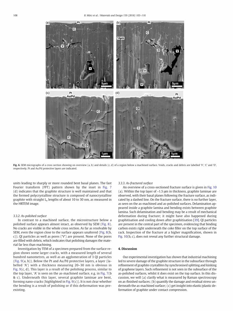
Fig. 6. SEM micrographs of a cross section showing on overview (a, b) and details (c, d) of a region below a machined surface. Voids, cracks and debris are labelled ‘V’, ‘C’ and ‘D’,respectively. Pt and Au/Pd protective layers are indicated.
108 B. März et al. / Materials and Design 159 (2018) 103–116
units leading to sharply or more rounded bent basal planes. The fastFourier transform (FFT) pattern shown by the inset in Fig. 7(d) indicates that the graphite structure is well maintained and thatthe formed polycrystalline structure is composed of nanocrystallinegraphite with straight La lengths of about 10 to 30 nm, as measured inthe HRTEM image.
3.3.2. As-polished surfaceIn contrast to a machined surface, the microstructure below a
polished surface appears almost intact, as observed by SEM (Fig. 8).No cracks are visible in the whole cross section. As far as resolvable bySEM, even the region close to the surface appears unaltered (Fig. 8(b,c)). QI particles as well as pores (‘V’) are present. None of the poresare filled with debris, which indicates that polishing damages themate-rial far less than machining.
Investigation by TEM of a specimen prepared from the surface re-gion shows some larger cracks, with a measured length of severalhundred nanometres, as well as an agglomeration of 3 QI particles(Fig. 9(a, b)). Below the Pt and Au/Pd protective layers, a layer (la-belled ‘A’) with a thickness measuring 20–30 nm is obvious inFig. 9(c, d). This layer is a result of the polishing process, similar tothe top layer, ‘A’ is seen on the as-machined surface, e.g. in Fig. 7(b& c). Underneath this layer, several graphite laminae are bent,forming nano-cracks (highlighted in Fig. 9(c)). It is not clear whetherthe bending is a result of polishing or if this deformation was pre-existing.
3.3.3. As-fractured surfaceAn overview of a cross-sectioned fracture surface is given in Fig. 10
(a). Within the top layer of ~1.5 μm in thickness, graphite laminae areobserved, with their basal planes following the fracture surface, as indi-cated by a dashed line. On the fracture surface, there is no further layer,as seen on the as-machined and as-polished surfaces. Delamination ap-peared inside a graphite lamina and bending exists between graphitelamina. Such delamination and bending may be a result of mechanicaldeformation during fracture; it might have also happened duringgraphitisation and cooling down after graphitisation [39]. QI particlesare present in the central part of the specimen, evidencing that bindingcarbon exists right underneath the coke filler on the top surface of therack. Inspection of the fracture at a higher magnification, shown inFig. 10(b, c), does not reveal any further structural damage.
4. Discussion
Our experimental investigation has shown that industrialmachiningled to severe damage of the graphite structure in the subsurface throughrefinement of graphite crystallites by synchronised splitting and kinkingof graphene layers. Such refinement is not seen in the subsurface of theas-polished surfaces, whilst it does exist on the top surface. In this dis-cussion, we will (a) clarify what is measured by Raman spectroscopyon as-finished surfaces; (b) quantify the damage and residual stress un-derneath the as-machined surface; (c) get insight into elastic/plastic de-formation of graphite under contact compression.

Fig. 7. TEM bright field (BF) views of the microstructure of a machined surface. (a) Overview; (b) upper region; (c) close to the surface; (d) HRTEM image and FFT (inset) of irregularlyoriented, bent graphite nano-crystallites. ‘A’ indicates a top layer of 35 nm thickness, voids ‘V’ and cracks ‘C’ are labelled as well.
109B. März et al. / Materials and Design 159 (2018) 103–116
4.1. Abrasion induced refinement of graphite crystal
Fracturing introduces no noticeable structural changes on the as-fractured surface, apart from nano-cracks that may have formedthrough exfoliation of graphene layers close to the fracture surface. Itis reasonable to believe that neither the in-plane dimension of graphitecrystallites, nor the C\\C bonding and local atomic arrangements, havebeen changed by the splitting process. Hence, the acquired Raman spec-tra on an as-fractured surface, shouldwell represent the structure insidean as-manufactured graphite, which has been supported by measure-ments of La from cross-sectional TEM images [17]. The probed averageposition of 1581.19 cm−1 for the G band on the as-fractured surface isso close to that on highly ordered pyrolytic graphite (HOPG) [40,41],evidencing that there is no extra elastic strain in the C\\C σ bonds.This allows the Raman data acquired on HOPG, i.e. the fracture surfaceof the polygranular graphite, to serve as a reference to understand theresults obtained on as-machined and as-polished surfaces.
Laboratory polishing generates a layer of carbon on the top surfaceshowing little diffraction contrast in the BF TEMmode. This layer is sim-ilar to that observed on an abrasion surface of a C\\C composite orcarbon-ceramic brake after experiencing heavy contact sliding [42]. Im-mediately under this abrasion layer, nano-cracks and bent graphitecrystals might have formed during polishing. However, as the grit sizeof the abrasives used, was only 40 nm in the final step, their penetrationdepth could not have exceeded this diameter and such features can beexpected on the top surface only. Compared to the as-fractured surface,values extracted from Raman spectra of the as-polished surface showsignificant changes, as shown in Table 1 and Fig. 4. The averaged La
estimated from ID/IG reduces from 110.84 ± 43.90 nm on the as-fractured surface to 22.14 ± 4.11 nm on the as-polished surface, andthe position of the G band maximum increases from 1581.19 ± 0.61to 1582.35± 0.80 cm−1 respectively, an increment of ~1 cm−1. Accord-ing to Ferrari and Robertson's interpretation [43], the polishing opera-tion has transformed the graphite into nanocrystalline graphitebecause the G band moves upward from 1581.19 cm−1 and the ID/IGratio increases, leading to smaller in-plane graphite crystallites. Sincethe determined La is much smaller than the thickness of the TEM spec-imens prepared by FIB, no HRTEM image is available to directly supportthe nanocrystalline structure of the abrasion layer. There is no evidencethat sp3 bonds exist in this layer, as no doublet in the D band appears.There is also no evidence showing that this abrasive layer has beentransformed into amorphous carbon, because the G band position didnot shift downwards, neither did the ID/IG ratio decrease to 0 [43].
Industry machining results in a similar thin layer of carbon at the topsurface. But, underneath, the graphite is subject to plastic deformationextending into far deeper regions, at about 12–14 μm (Fig. 6(b)). Thisleads to exfoliation of graphite into multiple graphite crystallites withgraphene planes kinked in different degrees, as shown in Fig. 7(d). Theaveraged La estimated from ID/IG reduces from 110.84 ± 43.90 nm onthe as-fractured surface to 21.64± 8.66 nm on the as-machined surface.The position of the G band maximum increases from 1581.19 ± 0.61 to1586.95 ± 0.80 cm−1 respectively, an increment of ~6 cm−1
. It seemsthis observed abrasion layer barely differs in terms of ID/IG, the trend ofthe G band shift and other features. Hence, we believe that nanocrystal-line graphitewith a thickness of tens of nanometres is formed by thema-chining process used by industry on the as-machined surface.

Fig. 8. SEM micrographs below a polished surface. An overview (a) of the cross section and details (b, c, d) are shown. Voids are labelled ‘V’.
110 B. März et al. / Materials and Design 159 (2018) 103–116
The small difference of La between the as-machined and as-polishedsurfaces implies that the main contribution to the Raman measure-ments was due to the abrasion layer on the top surface and the graphiteunderneath this layer had only a small contribution. However, it isnoted that the position of the G band maximum of the machined sur-face, shifts to much higher wavenumbers, compared to that of the as-polished surface. Ferrari & Robertson proposed that a change of thesp2 configuration from rings to olefinic groups shifts the G band tohigh frequencies because the higher vibrational modes of the olefinicgroups lie above the band limit of graphite. Such an sp2 configurationis observed in diamond like carbon (DLC) where the presence of sp3
bonds isolate sp2 dimers or chains in localised regions. As we do notsee clear D band doublets in our Raman data, as shown in Fig. 3, therewill not be many sp3 bonds in the abrasive layer, hence, short chainsor sp2 dimers. Thus, the observed shift of the G band must be relatedto residual stress or strain.
Frank et al. [44] recently studied the relationship betweenmeasuredRaman shift and stress level on both graphene and carbon fibres withdifferent Young's moduli. They proposed that the spectroscopic coeffi-cient correlating the shift of the G band (ΔωG, in cm−1) and uniaxialstress (σ, in MPa) are proportional to the neutral G band position(ωG0, in cm−1), as shown below:
ΔϖG ¼ −5
ϖG0σ ð2Þ
Based on our measurements of ωG0 on the as-fractured surface andthe shifts measured on as-polished and as-machined surfaces, the aver-age residual stress is −367 MPa and −1641 MPa, respectively. We
believe this incredibly high compression in the abrasion layer mightbe a consequence of plastic deformation, as detailed later. The muchlarger compression in the abrasion layer of the as-machined surface islikely due to even further higher compression in the subsurface, as evi-denced in the next section.
Based on our analysis, we could demonstrate that Raman spectros-copy acquired on a surface of graphite has a likely contribution from alayer of polycrystalline graphite with a thickness of tens nanometres,consisting of strongly refined crystallites due to smearing during theabrasion.
4.2. Subsurface refinement and stressed σ bonding induced by machining
The subsurface damage by industry machining is different from thatin the abrasion layer on the top of the as-polished surface, as indicatedby the diffraction contrast images where clear contrast becomes dis-cernible as shown in Fig. 7(a–c). This fact implies that the graphite crys-tallites are large enough, as supported by the HRTEM image in Fig. 7(d).To quantitatively establish the depth profile of the graphite crystallitesizes, we have averaged the La values estimated from the measured in-tensity ratio of D and G bands at the same depth, z, and plotted in Fig. 11(a–c). As noted in Section 4.1, a residual stress does exist on the as-machined surface and its depth profile is also plotted in Fig. 11.
An overview of the depth profiles of residual stress estimated fromthe shift of the G band and the La from ID/IG is presented in Fig. 11(a).The highest average level of compression, in a region near the surface,was about 2.5 GPa. This compression is about twice that measured onthe abrasion layer. At lower depths, the compression declines rapidly,followed by a further but milder decrease to a depth of about 200 μm

Fig. 9. TEM BF views of an as-polished surface. (a) Overview of the cross section with QI particles and cracks/voids ‘V’; (b) view of the surface region marked in (a) with a void ‘V’perpendicular to the beam direction; (c, d) detailed views showing a thin layer ‘A’ of 20–30 nm thickness as well as bending cracks.
111B. März et al. / Materials and Design 159 (2018) 103–116
where no more residual stress exists. It seems that a two-tier residualstress depth profile exists on the as-machined surface. To discern thetwo tiers, the estimated La is superimposed in the plots. Immediatelybelow the abrasion layer, the La value increases steadily from about20.1 nm to 105 nm into a depth of around 40 μm. Beyond this depth,the change of La shows no particular trend, and we believe that nomore graphite crystal refinement exists at these positions. The averagedLa of 116.4± 8.5 nm is similar to that measured on the as-fractured sur-face, as shown in Fig. 4(f). Hence, the depth profiles were studied
Fig. 10. TEM BF micrographs of a fracture surface. (a) Overview of the specimen cross-secti
separately for the depths below 40 μm, as shown in Fig. 11(b) and(c) respectively.
Within the 40 μm region, refinement of graphite crystallites by themachining operation occurred, and themeasured La versus depth, z, fol-lows a natural exponential function with a fitting confidence of R2 =0.8118:
La ¼ 13:442e0:052z ð3Þ
on; (b) graphite laminae near the surface, (c) detailed view of a bent stack of laminae.

Fig. 11. (a) Overview of depth profiles of residual stress (negative and positive values represent compression and tension respectively) estimated from the shift of the G band and La fromID/IG on the as-machined surface of graphite; (b–c) residual compression and refinement depth profiles on (b) top surface where graphite crystallites are refined and (c) underneath therefined graphite crystallite layer.
112 B. März et al. / Materials and Design 159 (2018) 103–116
The residual compression,σ, versus the depth is fittedwith a naturalexponential function, giving the following relation with a confidence ofR2 = 0. 9578:
σ ¼ 2783:1e−0:051z ð4Þ
As a first approximation, we believe the decay of residual compres-sion is tightly associated to the refinement of graphite crystallites, so alinear correlation between La and residual compression can be pro-posed:
σ ¼ kLa ð5Þ
where k is a constant. Based on Eqs. (3) and (4), we estimate a value of207 MPa/nm for k. Note, Eq. (5) may apply only to a refined graphitestructure by mechanical deformation, not developed through thermalequilibration.
At depths beyond 40 μm, there is no further refinement. However,significantly high compression is maintained, as shown in Fig. 11(c).We can use a linear fit to the data, but the confidence is very low. Themain factors that lie outside the linear fitting are the three valleys,marked as A, B and C. We believe that the stressing was discontinueddue to the existence of a large void/crack as shown in Fig. 7(a). Bytreating the data points in these three regions as outliers, the remainingdata show a perfect linear relation,with R2=0.9825, between the com-pression levels and the depths:
σ ¼ −2:9023zþ 467:16 ð6Þ
By accounting for both, refinement and residual compression, wemay propose the following model for the machining-induced surfacedamage: (a) A compression on the surface by a machining tool leadsto buckling and splitting of graphite crystallites, seen as refinement;(b) the bending and splitting of the graphene layers puts the σ bondsunder compression or tension but the compression dominates withinthe refinement layer; (c) the plastically deformed refinement layer can-not fully recover after removal of the machining tool and a residualstrain is maintained within the region underneath the refined material.Atomistic simulations were conducted to get an insight into the plasticdeformation process, or refinement of graphite crystals, as discussedin Section 4.3.
4.3. Elastic/plastic deformation and graphite refinement by contactdeformation
In order to understand how the graphite responds to the surfacema-chining, we perform indentation simulations upon a single crystal ofgraphite, usingmolecular dynamics (MD). AllMD simulationswere per-formed using the latest stable version of LAMMPS (16 Mar 2018) [45]available at http://lammps.sandia.gov. We used the AIREBO [46] poten-tial with a cut-off of 3 sigma (pair_style airebo 3.0). This gives a maxi-mum cut-off of the Lennard Jones term of 10.2 Å. The AIREBOpotential is an extension of the reactive empirical bond-order (REBO)potential developed by Brenner [47–49]. The REBO potential was origi-nally developed for diamond structures, and is therefore not suitable forgraphite. The AIREBO potential includes additional dispersion, torsion,and non-bonded interactions, which models the hexagonal rings ofthe graphene sheets and the inter-layer bonding between them.

113B. März et al. / Materials and Design 159 (2018) 103–116
To access large length scales, we use a cylindrical indenter upon athin wafer of graphite. The thin width was set to 12 Å, which is thesmallest length that ensures that the atoms do not interact with them-selves across the periodic boundary. The x and z dimensions of the sin-gle crystal graphite wafer are 100 nm. There was a total of 1.5 millioncarbon atoms in the simulation box.
Fig. 12(a–c) shows a snapshot of the graphitewaferwith an indenterradius of 5 nm, pressed into the wafer in the c direction (z in the im-ages). Here we used periodic boundaries in the x and y directions, andthe base was fixed. There was a 25 Å thermostat region set to 300 K atthe base. The images show the indenter at a depth of 15 nm. The in-denter was pressed into the wafer at a fixed speed of 1 Å/ps (100 m/s)to a depth of 20 nm. Fig. 12(a) clearly shows the σ bonds are stretchedaround the sharp indenter. The graphene planes curved around the in-denter and no carbon bonds were broken, indicating that the responseis elastic and reversible at this depth. As there is no space for the mate-rial to go, the graphene planes are also compressed closer together. Thehistogram in Fig. 12(c) shows that the σ bonds become increasinglystretched at greater indentation depths. Beyond 20 nm, the σ bondsbreak leading to a catastrophic failure of the graphite crystal due tothe release of the strain energy. The corresponding elongation is about25%, similar to the elongation limit reported by [50].
Fig. 12(d–f) shows a snapshot of the graphite wafer with a 50 nm ra-dius indenter pressed in the x direction. Here the y and z boundaries areperiodic, and the left x edge is fixed. The 25 Å thermostat region wasalso placed along the left x edge. There is a small compression of the σ
(a) (b)
(d) (e)
Fig. 12. (a–c) Snapshot of a cylindrical indenter with a radius of 5 nm at an indentation depth o(a) Coloured by average σ bond length, and (b) coloured by displacement in the y direction toindenter at depths from 5 to 20 nm. (d–f) Snapshot of a cylindrical indenter with a radius owafer (100 nm × 100 nm × 1.2 nm). (d) Coloured by average σ bond length, and (e) colo(f) Histograms of the σ bond length with the indenter at depths from 5 to 17.85 nm. (For intweb version of this article.)
bonds under the indenter, which can be seen in Fig. 12(d), and also inthe histograms in Fig. 12(f). We see that the graphite planes formmany kink bands and are also compressed closer together (Fig. 13(e)).
Simulation results shown in Fig. 12 reveal the following: (a) whencompression is applied normal to the basal planes of a graphite crystal,there is no plastic deformation, hence no residual strain when pressureis released, but C\\C bond breaking can happen when the pressure ishigh enough, directly leading to graphite crystal refinement. (b) whencompression is applied along the basal planes, plastic deformation hap-pens through the formation of kinks, leading to a residual compressioninside this region. The kinking itself is the major contributor for the re-duced coherent length, La, though C\\C breaking can still happen whenthe pressure is large enough.
Fig. 13(a–c) shows the same system as Fig. 12(d–f), but this time theinitial structure contained a 10 nm×100 nmvoid at the top edge. As theindenter is pressed into the wafer, it can expand in the c direction to fillthis gap. As a result, more distortion of the graphite planes is observed.Also, the σ bonds do not change their lengths significantly. Kink bandswith triangular shaped voids along the kink are also observed inFig. 13(a–b). Fig. 13(d–f) shows a similar smaller system to Fig. 13(a–c), however, this indenter is a sharper quadratic shape. Also, theatoms around the indenter are fixed. More distortion and folding ofthe planes is observed in this case, due to the greater strain in thissystem.
Simulation results shown in Fig. 13 reveal that when free space ex-ists within a graphite crystal under compression, significantly large
(c)
(f)
0
2000
4000
6000
8000
10000
12000
14000
0.135 0.136 0.137 0.138 0.139 0.14 0.141 0.142 0.143 0.144 0.145 0.146 0.147 0.148
Coun
t
Sigma bond length, nm
0 nm indenta�on
5 nm indenta�on
10 nm indenta�on
15 nm indenta�on
20 nm indenta�on
0
2000
4000
6000
8000
10000
12000
14000
0.135 0.136 0.137 0.138 0.139 0.14 0.141 0.142 0.143 0.144 0.145 0.146 0.147 0.148
Coun
t
Sigma bond length, nm
0 nm indenta�on
5 nm indenta�on
10 nm indenta�on
15 nm indenta�on
17.85 nm indenta�on
f 15 nm in the c direction of a single crystal graphite wafer (100 nm × 100 nm × 1.2 nm).allow visualisation of the graphene planes. (c) Histograms of the σ bond length with thef 50 nm at an indentation depth of 15 nm in the x direction of a single crystal graphiteured by displacement in the y direction to allow visualisation of the graphene planes.erpretation of the references to colour in this figure legend, the reader is referred to the

(a) (b) (c)
(d) (e) (f)
0
2000
4000
6000
8000
10000
12000
14000
0.135 0.136 0.137 0.138 0.139 0.14 0.141 0.142 0.143 0.144 0.145 0.146 0.147 0.14
Coun
t
Sigma bond length, nm
0 nm indenta�on
5 nm indenta�on
10 nm indenta�on
15 nm indenta�on
17.5 nm indenta�on
0
500
1000
1500
0.135 0.136 0.137 0.138 0.139 0.14 0.141 0.142 0.143 0.144 0.145 0.146 0.147 0.14
Coun
t
Sigma bond length, nm
0 nm indenta�on
5 nm indenta�on
10 nm indenta�on
15 nm indenta�on
20 nm indenta�on
Fig. 13. Snapshot of a cylindrical indenter with a radius of 50 nm at an indentation depth of 15 nm in the x direction of a single crystal graphite wafer (100 nm× 100 nm× 1.2 nm). Thisstructure initially had a void 10 nm × 100 nm at the top edge. (a) Coloured by average σ bond length, and (b) coloured by displacement in the y direction to allow visualisation of thegraphene planes. (c) Histograms of the σ bond length with the indenter at depths from 5 to 17.5 nm. (d–f) Snapshot of a sharp quadratic indenter with a radius of 20 nm at a depth of15 nm in the x direction in a single crystal graphite wafer (40 nm × 40 nm × 1.2 nm). (d) Coloured by average σ bond length, and (e) coloured by displacement in the y direction toallow visualisation of the graphene planes. (f) Histograms of the σ bond length with the indenter at depths from 5 to 20 nm. The sharp peak is due to a layer of fixed atoms around theindenter. (For interpretation of the references to colour in this figure legend, the reader is referred to the web version of this article.)
114 B. März et al. / Materials and Design 159 (2018) 103–116
plastic deformation can occur. This includes splitting of graphene planesto form multiple layered graphene units and large kinks, similar to theobserved structures seen with HRTEM shown in Fig. 7(d). Free spaceswidely exist inside a synthetic graphite in the form of nano/micro-cracks and pores [51–53].
Whilst the contact loading conditions shown in Fig. 12 and Fig. 13may not represent all loading context during machining or polishing,the plastic deformation and graphite crystal refinement processeshave been clearly demonstrated.
5. Conclusions
Graphite surfaces, industry machined or laboratory polished, showan abrasion surface layer with a thickness of tens nanometres and astructure consisting of refined polycrystalline graphite with almost thesame La, ~20 nm. The C\\C σ bonds in this layer are under compressionat a level of 367 MPa for the as-polished and 1641 MPa for the as-machined surface.
Underneath the as-machined surface, three layers with differentstructural featureswere identified. Near the top surfacewith a thicknessof ~14 μm, large pores were filled with graphite fragments and somecracks were also filled, leading to a higher density than the bulk
graphite. Inside a depth up to ~35–40 μm, graphite crystallites were re-fined by the machining operation with the smallest La measured on thesurface. The refinement is evidenced by HRTEM images showing split-ting of graphite intomultiple layered graphene units with bending, sup-ported by the molecular dynamic simulation. In this refined layer, theC\\C σ bond is under compression with the highest level N 2500 MPaon the surface. Both the degree of crystal refinement, and the compres-sion level, decay exponentially with the depth.
σ or 1=La ¼ βe−αz
with the compression and La showing a linear relationship (α and βare fitting parameters). In a region beyond the refined region compres-sion exists, which follows a linear decay up to a depth of around 200 μm.
Acknowledgements
We gratefully acknowledge the support of the EPSRC AdvancedMa-terials for Nuclear Fission programme under UNIGRAF: Understandingand Improving Graphite for Nuclear Fission with the grant numbersEP/M018822/1, EP/M018598/1 and EP/M018679/1. The authors ac-knowledge use of facilities within the Loughborough Materials

115B. März et al. / Materials and Design 159 (2018) 103–116
Characterization Centre. Special thanks are extended to Mr. Dai Huangfrom Sinosteel Advanced Materials Co. Ltd. to grant researchers inUNIGRAF to access their experimental nuclear graphite grades and pro-vide great support in sample preparation and supply.
Author contribution
Benjamin März: designed and performed the experiments; proc-essed the data; initiated the writing.
Kenny Jolley: Performed the atomistic modelling; supported thewriting.
Roger Smith: Supported the atomistic modelling and writing.Houzheng Wu: Conceived the presented ideas; analysed the data
and derived the model; led the writing.
References
[1] G. Haag, D. Mindermann, G. Wilhelmi, H. Persicke, W. Ulsamer, Development of re-actor graphite, J. Nucl. Mater. 171 (1990) 41–48, https://doi.org/10.1016/0022-3115(90)90345-N.
[2] P. Lian, J. Song, Z. Liu, J. Zhang, Y. Zhao, Y. Gao, Z. Tao, Z. He, L. Gao, H. Xia, Q. Guo, P.Huai, X. Zhou, Preparation of ultrafine-grain graphite by liquid dispersion techniquefor inhibiting the liquid fluoride salt infiltration, Carbon 102 (2016) 208–215,https://doi.org/10.1016/j.carbon.2016.02.018.
[3] X.W. Zhou, Y.P. Tang, Z.M. Lu, J. Zhang, B. Liu, Nuclear graphite for high temperaturegas-cooled reactors, Xinxing Tan Cailiao New Carbon Mater. 32 (2017) 193–204,https://doi.org/10.1016/S1872-5805(17)60116-1.
[4] M.A. Snead, A.A. Campbell, Y. Katoh, D. Huang, H. Wu, H. Yang, H. Li, T.D. Burchell, C.Contescu, Sinosteel AMC Graphite Irradiation Program at ORNL, in: INGSM-17, Vi-enna, IAEA, Vienna, 2016.
[5] M.W. Davies, Graphite Core Design in UK Reactors, 1996 10http://www.iaea.org/inis/collection/NCLCollectionStore/_Public/28/008/28008804.pdf.
[6] J.W. Geringer, A.A. Campbell, J.D. Arregui-Mena, Y. Katoh, D. Huang, H. Wu, H. Yang,H. Li, Y. Lee, C. Contescu, Sinosteel AMC graphite irradiation program at ORNL, Int.Nucl. Graph. Spec. Meet. INGSM-2017, Baltimore, MD, 2017.
[7] D.L. Selby, G.S. Smith, Scientific upgrades at the high flux isotope reactor at OakRidge National Laboratory, Nucl. News 53 (2010) 35.
[8] R.L. McCreery, Advanced carbon electrode materials for molecular electrochemistry,Chem. Rev. 108 (2008) 2646–2687, https://doi.org/10.1021/cr068076m.
[9] M. Le Guillou, J.N. Rouzaud, D. Deldicque, N. Toulhoat, Y. Pipon, N. Moncoffre, Struc-tural and nanostructural behavior of deuterium implanted highly ordered pyrolyticgraphite investigated by combined high resolution transmission electron micros-copy, scanning electron microscopy and Raman microspectrometry, Carbon 94(2015) 277–284, https://doi.org/10.1016/j.carbon.2015.06.065.
[10] S. Mathew, B. Joseph, B.R. Sekhar, B.N. Dev, X-ray photoelectron and Raman spectro-scopic studies of MeV proton irradiated graphite, Nucl. Instrum. Methods Phys. Res.,Sect. B 266 (2008) 3241–3246, https://doi.org/10.1016/j.nimb.2008.03.233.
[11] A.C. Ferrari, J. Robertson, Resonant Raman spectroscopy of disordered, amorphous,and diamondlike carbon, Phys. Rev. B 64 (2001), 075414. https://doi.org/10.1103/PhysRevB.64.075414.
[12] I. Manika, J. Maniks, R. Zabels, J. Gabrusenoks, M. Krause, M. Tomut, K. Schwartz,Nanoindentation and Raman spectroscopic study of graphite irradiated with swift238U ions, Fullerenes, Nanotubes, Carbon Nanostruct. 20 (2012) 548–552, https://doi.org/10.1080/1536383x.2012.656064.
[13] M.R. Ammar, N. Galy, J.N. Rouzaud, N. Toulhoat, C.E. Vaudey, P. Simon, N. Moncoffre,Characterizing various types of defects in nuclear graphite using Raman scattering:heat treatment, ion irradiation and polishing, Carbon 95 (2015) 364–373, https://doi.org/10.1016/j.carbon.2015.07.095.
[14] M.A. Pimenta, G. Dresselhaus, M.S. Dresselhaus, L.G. Cançado, A. Jorio, R. Saito,Studying disorder in graphite-based systems by Raman spectroscopy, Phys. Chem.Chem. Phys. 9 (2007) 1276–1291, https://doi.org/10.1039/b613962k.
[15] M.R. Ammar, J.N. Rouzaud, C.E. Vaudey, N. Toulhoat, N. Moncoffre, Characterizationof graphite implantedwith chlorine ions using combined Ramanmicrospectrometryand transmission electron microscopy on thin sections prepared by focused ionbeam, Carbon 48 (2010) 1244–1251, https://doi.org/10.1016/j.carbon.2009.11.049.
[16] F. Adar, E. Lee, S. Mamedov, A. Whitley, Experimental evaluation of the depth reso-lution of a Raman microscope, Microsc. Microanal. 16 (2010) 360–361, https://doi.org/10.1017/S1431927610055352.
[17] B.März, K. Jolley, T.J. Marrow, Z. Zhou, M. Heggie, R. Smith, H. Wu,Mesoscopic struc-ture features in synthetic graphite, Mater. Des. 142 (2018) 268–278, https://doi.org/10.1016/j.matdes.2018.01.038.
[18] B. März, K. Jolley, T.J. Marrow, Z. Zhou, M. Heggie, R. Smith, H. Wu, Data related tothe mesoscopic structure of iso-graphite for nuclear applications, Data Brief 19(2018) 651–659, https://doi.org/10.1016/j.dib.2018.05.003.
[19] H. Yang, H. Li, D. Huang, H. Wu, M. Snead, A.A. Campbell, Y. Katoh, T.D. Burchell,Specimen size effect on type-I fracture toughness (K_IC) measurements of finegrain nuclear grade graphite, Int. Nucl. Graph. Spec. Meet. INGSM-16, Nottingham,2015.
[20] H.M. Freeman, A.N. Jones, M.B. Ward, F.S. Hage, N. Tzelepi, Q.M. Ramasse, A.J. Scott,R.M.D. Brydson, On the nature of cracks and voids in nuclear graphite, Carbon 103(2016) 45–55, https://doi.org/10.1016/j.carbon.2016.03.011.
[21] R. Krishna, A.N. Jones, R. Edge, B.J. Marsden, Residual stress measurements in poly-crystalline graphite with micro-Raman spectroscopy, Radiat. Phys. Chem. 111(2015) 14–23, https://doi.org/10.1016/j.radphyschem.2015.02.007.
[22] R. Krishna, A.N. Jones, B.J. Marsden, Transmission electron microscopy, Raman andX-ray photoelectron spectroscopy studies on neutron irradiated polycrystallinegraphite, Radiat. Phys. Chem. 107 (2015) 121–127, https://doi.org/10.1016/j.radphyschem.2014.10.005.
[23] C. Karthik, J. Kane, D.P. Butt, W.E. Windes, R. Ubic, Neutron irradiation induced mi-crostructural changes in NBG-18 and IG-110 nuclear graphites, Carbon 86 (2015)124–131, https://doi.org/10.1016/j.carbon.2015.01.036.
[24] C. Karthik, J. Kane, D.P. Butt, W.E. Windes, R. Ubic, Microstructural characterizationof next generation nuclear graphites, Microsc. Microanal. 18 (2012) 272–278,https://doi.org/10.1017/S1431927611012360.
[25] K.Y. Wen, J. Marrow, B.J. Marsden, Nanostructures of carbon in nuclear graphite, J.Phys. Conf. Ser. 126 (2008), 012056. https://doi.org/10.1088/1742-6596/126/1/012056.
[26] K.Y. Wen, T.J. Marrow, B.J. Marsden, The microstructure of nuclear graphite binders,Carbon 46 (2008) 62–71, https://doi.org/10.1016/j.carbon.2007.10.025.
[27] S.S. Jones, E.M.Woodruff, Microstructure of carbon blacks in pitch-bonded graphitesand structural changes produced by gas-graphite oxidation reactions, Carbon 9(1971) 259–264, https://doi.org/10.1016/0008-6223(71)90044-3.
[28] K. Lafdi, S. Bonnamy, A. Oberlin, Tem studies of coal tars: crude tar and its insolublefractions, Carbon 28 (1990) 57–63, https://doi.org/10.1016/0008-6223(90)90093-E.
[29] M. Lasithiotakis, B.J. Marsden, T. JamesMarrow, Annealing of ion irradiation damagein nuclear graphite, J. Nucl. Mater. 434 (2013) 334–346, https://doi.org/10.1016/j.jnucmat.2012.12.001.
[30] A.C. Ferrari, J.C. Meyer, V. Scardaci, C. Casiraghi, M. Lazzeri, F. Mauri, S. Piscanec, D.Jiang, K.S. Novoselov, S. Roth, A.K. Geim, Raman spectrum of graphene and graphenelayers, Phys. Rev. Lett. 97 (2006) 1–4, https://doi.org/10.1103/PhysRevLett.97.187401.
[31] R.P. Vidano, D.B. Fischbach, L.J. Willis, T.M. Loehr, Observation of Raman bandshifting with excitation wavelength for carbons and graphites, Solid State Commun.39 (1981) 341–344, https://doi.org/10.1016/0038-1098(81)90686-4.
[32] R.J. Nemanich, S.A. Solin, First- and second-order Raman scattering from finite-sizecrystals of graphite, Phys. Rev. B 20 (1979) 392–401, https://doi.org/10.1103/PhysRevB.20.392.
[33] A.C. Ferrari, Raman spectroscopy of graphene and graphite: disorder, electron-phonon coupling, doping and nonadiabatic effects, Solid State Commun. 143(2007) 47–57, https://doi.org/10.1016/j.ssc.2007.03.052.
[34] M. Nakamizo, K. Tamai, Raman spectra of the oxidized and polished surfaces ofcarbon, Carbon 22 (1984) 197–198, https://doi.org/10.1016/0008-6223(84)90216-1.
[35] O.A. Maslova, M.R. Ammar, G. Guimbretière, J.N. Rouzaud, P. Simon, Determinationof crystallite size in polished graphitized carbon by Raman spectroscopy, Phys.Rev. B: Condens. Matter Mater. Phys. 86 (2012) 1–5, https://doi.org/10.1103/PhysRevB.86.134205.
[36] F. Tuinstra, J.L. Koenig, Raman spectrum of graphite, J. Chem. Phys. 53 (1970)1126–1130, https://doi.org/10.1063/1.1695699.
[37] D.S. Knight, W.B. White, Characterization of diamond films by Raman spectroscopy,J. Mater. Res. 4 (1989) 385–393, https://doi.org/10.1557/JMR.1989.0385.
[38] L.G. Cançado, K. Takai, T. Enoki, M. Endo, Y.A. Kim, H. Mizusaki, A. Jorio, L.N. Coelho,R. Magalhães-Paniago, M.A. Pimenta, General equation for the determination of thecrystallite size La of nanographite by Raman spectroscopy, Appl. Phys. Lett. 88(2006) 16–19, https://doi.org/10.1063/1.2196057.
[39] S. Mrozowski, Mechanical strength, thermal expansion and structure of cokes andcarbons, Proc. 1st 2nd Conf. Carbon 1956, pp. 31–45.
[40] S. Reich, C. Thomsen, Raman spectroscopy of graphite, Philos. Transact. A Math.Phys. Eng. Sci. 362 (2004) 2271–2288, https://doi.org/10.1098/rsta.2004.1454.
[41] Y. Wang, D.C. Alsmeyer, R.L. Mccreery, Raman spectroscopy of carbon materials:structural basis of observed spectra, Chem. Mater. 2 (1990) 557–563, https://doi.org/10.1021/cm00011a018.
[42] Y. Wang, H. Wu, Microstructure of friction surface evolution of carbon fibre rein-forced carbon/silicon carbide (C f/C-SiC) composites, J. Eur. Ceram. Soc. 30 (2010)3187–3201, https://doi.org/10.1016/j.jeurceramsoc.2010.07.019.
[43] A.C. Ferrari, J. Robertson, Interpretation of Raman spectra of disordered and amor-phous carbon, Phys. Rev. B 61 (2000) 14095–14107, https://doi.org/10.1103/PhysRevB.61.14095.
[44] O. Frank, G. Tsoukleri, I. Riaz, K. Papagelis, J. Parthenios, A.C. Ferrari, A.K. Geim, K.S.Novoselov, C.Galiotis, Development of a universal stress sensor for graphene and car-bon fibres, Nat. Commun. 2 (2011) 255–257, https://doi.org/10.1038/ncomms1247.
[45] S. Plimpton, Fast parallel algorithms for short-range molecular dynamics, J. Comput.Phys. 117 (1995) 1–19, https://doi.org/10.1006/jcph.1995.1039.
[46] S.J. Stuart, A.B. Tutein, J.A. Harrison, A reactive potential for hydrocarbons with inter-molecular interactions, J. Chem. Phys. 112 (2000) 6472–6486, https://doi.org/10.1063/1.481208.
[47] D.W. Brenner, Empirical potential for hydrocarbons for use in simulating the chem-ical vapor deposition of diamond films, Phys. Rev. B 42 (1990) 9458–9471, https://doi.org/10.1103/PhysRevB.42.9458.
[48] D.W. Brenner, J.A. Harrison, C.T. White, R.J. Colton, Molecular dynamics simula-tions of the nanometer-scale properties of compressed Buckminsterfullerene,Thin Solid Films 206 (1991) 220–223, https://doi.org/10.1016/0040-6090(91)90425-W.
[49] D.W. Brenner, Erratum: empirical potential for hydrocarbons for use in simulat-ing the chemical vapor deposition of diamond films [Phys. Rev. B 42, 9458(1990)], Phys. Rev. B 46 (1992) 1948, https://doi.org/10.1103/PhysRevB.46.1948.2.

116 B. März et al. / Materials and Design 159 (2018) 103–116
[50] V.M. Pereira, A.H. Castro Neto, N.M.R. Peres, Tight-binding approach to uniaxialstrain in graphene, Phys. Rev. B: Condens. Matter Mater. Phys. 80 (2009) 1–8,https://doi.org/10.1103/PhysRevB.80.045401.
[51] D. Liu, D. Cherns, Nano-cracks in a synthetic graphite composite for nuclear applica-tions, Philos. Mag. 6435 (2018) 1–12, https://doi.org/10.1080/14786435.2018.1433886.
[52] J. Kane, C. Karthik, D.P. Butt, W.E. Windes, R. Ubic, Microstructural characterizationand pore structure analysis of nuclear graphite, J. Nucl. Mater. 415 (2011)189–197, https://doi.org/10.1016/j.jnucmat.2011.05.053.
[53] D. Liu, K. Mingard, O.T. Lord, P. Flewitt, On the damage and fracture of nucleargraphite at multiple length-scales, J. Nucl. Mater. 493 (2017) 246–254, https://doi.org/10.1016/j.jnucmat.2017.06.021.