MATERIAL AND DEVICE DESIGN FOR ORGANIC OPTOELECTRONICS
194
MATERIAL AND DEVICE DESIGN FOR ORGANIC OPTOELECTRONICS Jack W. Levell A Thesis Submitted for the Degree of PhD at the University of St Andrews 2011 Full metadata for this item is available in Research@StAndrews:FullText at: http://research-repository.st-andrews.ac.uk/ Please use this identifier to cite or link to this item: http://hdl.handle.net/10023/2066 This item is protected by original copyright This item is licensed under a Creative Commons License
Transcript of MATERIAL AND DEVICE DESIGN FOR ORGANIC OPTOELECTRONICS
MATERIAL AND DEVICE DESIGN FOR ORGANICOPTOELECTRONICS
Jack W. Levell
A Thesis Submitted for the Degree of PhDat the
University of St Andrews
2011
Full metadata for this item is available inResearch@StAndrews:FullText
at:http://research-repository.st-andrews.ac.uk/
Please use this identifier to cite or link to this item:http://hdl.handle.net/10023/2066
This item is protected by original copyright
This item is licensed under aCreative Commons License
Material and Device Design for Organic Optoelectronics
Jack W. Levell
This thesis is submitted in partial fulfilment for the degree of PhD
at the University of St Andrews
May 2011

i
ii
Abstract
This thesis describes investigations into the photophysical properties of luminescent
materials and their application in optoelectronic devices such as light emitting diodes
and photodetectors. The materials used were all solution processable because of the
interest in low cost processing of organics.
I have investigated the photophysics of 1,4,5,8,9,12-hexamethyltriphenylene, a
triphenylene derivative which has its luminescence enhanced by the addition of
methyl groups. These groups change the planar shape of the triphenylene molecule
into a twisted one, changing the symmetry of the molecule and increasing its dipole
moment in absorption and emission by ~4 fold. This increased its rate of radiative de-
excitation by ~20 times. In addition, the twisted shape of the molecule prevents
intermolecular interactions and concentration effects from affecting the luminescence.
This results in an efficient solid-state photoluminescence quantum yield of 31%.
This thesis also includes an investigation into phosphorescent polymer dendrimers,
designed to have suitable viscosities in solution for inkjet printed OLED applications.
A photophysical study of the intra-chain aggregation effects on the luminescence was
undertaken in both homopolymers and copolymers with high energy gap spacer units.
Using double dendrons to increase the steric protection of the luminescent cores, the
best homopolymers achieved 12.1% external quantum efficiency (39.3 cd/A) at 100
cd/m2 brightness and the best co-polymer achieved 14.7% EQE (48.3 cd/A) at 100
cd/m2. This compares favourably with 11.8% EQE for the best phosphorescent
polymer and 16% for the best solution processed dendrimer OLED previously
reported.
Finally I have applied a solution processed enhancement layer to silicon photodiodes
to enhance their ultraviolet response. Using a blend of materials to give favourable
absorption and emission properties, 61% external quantum efficiency was achieved at
200 nm, which is better than the 20-30% typical for vacuum deposited lumogen
enhancement layers used commercially.

iii
iv
1. Candidate’s Declarations
I, Jack William Levell, hereby certify that this thesis, which is approximately 45,000 words in length, has been written by me, that it is the record of work carried out by me and that it has not been submitted in any previous application for a higher degree. I was admitted as a research student in September 2007 and as a candidate for the degree of Doctor of Philosophy in September 2007 the higher study for which this is a record was carried out in the University of St Andrews between 2007 and 2011.
Date: 18/05/10 Signature of candidate: Jack W. Levell
2. Supervisor’s Declarations
I hereby certify that the candidate has fulfilled the conditions of the Resolution and Regulations appropriate for the degree of Doctor of Philosophy in the University of St Andrews and that the candidate is qualified to submit this thesis in application for that degree.
Date: 18/05/10 Signature of supervisor: Ifor D. W. Samuel
3. Permission for Electronic Publication:
In submitting this thesis to the University of St Andrews I understand that I am giving permission for it to be made available for use in accordance with the regulations of the University Library for the time being in force, subject to any copyright vested in the work not being affected thereby. I also understand that the title and the abstract will be published, and that a copy of the work may be made and supplied to any bona fide library or research worker, that my thesis will be electronically accessible for personal or research use unless exempt by award of an embargo as requested below, and that the library has the right to migrate my thesis into new electronic forms as required to ensure continued access to the thesis. I have obtained any third-party copyright permissions that may be required in order to allow such access and migration, or have requested the appropriate embargo below. The following is an agreed request by candidate and supervisor regarding the electronic publication of this thesis: Access to all of printed copy but embargo of all of electronic publication of thesis for a period of 1 year on the following ground: Publication would preclude future publication
Date: 18/05/10 Signature of candidate: Jack W. Levell
Date: 18/05/10 Signature of supervisor: Ifor D. W. Samuel

v
vi
Acknowledgements
This thesis and the work within it would literally not have been possible without the
help of a large number of people, some of whom I’ve listed below.
Everyone within the organic semiconductor optoelectronics (OSO) group has been
very helpful and has made my time here a pleasure. I’d like to thank Ruth Harding
and Stuart Stevenson for training me in experimental techniques. Arvydas Ruseckas
was lots of help with photophysics problems, in particular on the HMTP project.
Graham Turnbull has been an excellent second supervisor and his constant
cheerfulness has been reassuring throughout. Most of all I’d like to thank Mario
Giardini. The photodiodes project was based on his original idea but he has also
shown me that solving problems for a living is great fun.
Thanks go to Yi Wang and Trent Galow at the University of Edinburgh for letting me
work on their fascinating HMTP material. The phosphorescent polymer work would
not have happened without Paul Burn’s vision and the hard work of Jack Gunning in
Oxford, and Wen-Yong Lai and Shih-Chun Lo in Queensland. Wen-Yong in
particular worked tirelessly and those materials presented in this thesis are only a
small fraction of his total output! I wish him all the best at his new posting in Nanjing.
I’d also like to thank George Robb and Steve Balfour, without whom nothing would
ever work in the cleanroom. I’m sorry about that fire alarm but if George could have a
look at the health and safety considerations concerned with throwing people into the
physics pond I would be very grateful.
Outside of work I’ve been kept sane by many people including my family, Ken
Armstrong, Saif Ur-Rehman, Tosca Lynch, Nick Drewett and Fiona Howe. Life
would also have been quite dull without my gaming group: Steve Grant, Alasdair
Lymer, George Crossley and Joseph Collins who’ve helped with the other ~200 page
document I’ve produced during my time here.
Finally I’d like to thank Ifor Samuel, my supervisor, for putting up with me and
carefully reading through the many hundreds of pages of terrible English, red pen in
hand.

vii

viii
To my parents, Bruce and Sally.
For everything.

ix
x
“Understanding is a three-edged sword.”
- Ambassador Kosh, Babylon 5

xi
xii
Table of Contents
1. Introduction …………………………………………………………………. 1
2. Organic Semiconductors……………………………………………………. 5 2.1 Overview …………………………………………………………………… 5
2.2 Semiconductors …………………………………………………………… 5
2.3 Organic Semiconductors …………………………………………………… 7
2.4 Charge Transport ………………………………………………………….... 12
2.5 Excited States: Excitons …………………………………………………… 14
2.6 Organic Semiconductors for Devices …………………………………… 16
2.7 Conclusion …………………………………………………………… 20
3. Organic Light Emitting Diodes……………………………………………… 23 3.1 Introduction ……………………………………………………………. 23
3.1.2 OLEDs vs. LCD Displays ……………………………………. 24
3.1.3 OLEDs for Lighting ……………………………………………. 26
3.2 Characterising OLEDs: Device Parameters ……………………………. 26
3.2.1 Power Efficiency ……………………………………………. 26
3.2.2 Brightness ……………………………………………………. 27
3.2.3 CIE Colour Co-ordinates ……………………………………. 28
3.2.4 Colour Rendering Index ....…………………………………. 30
3.2.5 External Quantum Efficiency and Luminous Efficiency ……. 31
3.2.6 Lifetime ……………………………………………………………. 31
3.3 Light Emission In OLEDs ……………………………………………. 32
3.4 Materials for OLED devices …………………………………………… 35
3.4.1 Host-Guest Blending …………………………………………… 36
3.4.2 Phosphorescent Emitters …………………………………… 36
3.4.3 Aggregated States: Dimers and Excimers …………………… 43
3.4 Design of OLEDs …………………………………………………………… 46
3.4.1 Charge Injection …………………………………………… 46
3.4.2 Electrode Quenching …………………………………………… 48
3.4.3 Charge Transport Layers …………………………………… 48
3.4.4 Light Extraction …………………………………………… 50
xiii
4. Experimental Methods ……………………………………………………… 56 4.1 Overview …………………………………………………………………… 56
4.2 Phosphorescence Quenching by Oxygen …………………………………… 57
4.3 Absorption and Photoluminescence Spectra …………………………… 58
4.4 Photoluminescence Quantum Yield (PLQY) …………………………… 58
4.4.1 Solution PLQY …………………………………………………… 58
4.4.2 Film PLQY …………………………………………………… 60
4.4.3 Powder PLQY …………………………………………………… 62
4.4.4 CCD and Integrating Sphere Method …………………………… 63
4.5 Time-Correlated Single Photon Counting …………………………… 64
4.6 OLED Device Fabrication …………………………………………… 65
4.7 OLED Characterisation …………………………………………………… 69
4.7.1 External Quantum Efficiency Calculation …………………… 70
4.7.2 Luminous Efficiency Calculation …………………………… 72
5. Fluorescent Enhancement Using a Twisted Tripheneylene Derivative 76 5.1 Introduction …………………………………………………………… 76
5.2 Measuring Oscillator Strength …………………………………………… 78
5.3 Results and Discussion …………………………………………………… 81
5.3.1 Absorption Properties …………………………………………… 81
5.3.2 Emission Properties …………………………………………… 84
5.4 OLED Measurements …………………………………………………… 92
5.5 Conclusion …………………………………………………………… 92
6. Poly(dendrimer) Iridium Complexes………………………………………... 95 6.1 Introduction ……………………………………………………………. 95
6.2 Introduction to Phosphorescent Polymers ……………………………. 96
6.3 Ir(ppy)2(acac) Based Polymers ……………………………………………. 97
6.3.1 Ir(ppy)2(acac) Solution Properties ……………………………. 98
6.3.2 Ir(ppy)2(acac) Film Properties ……………………………………. 101
6.3.3 Dendronised Ir(ppy)2(acac) Polymer Properties ……………. 102
6.4 Ir(ppy)2(ptz) Based Poly(Dendrimers) ……………………………………. 106
6.4.1 Ir(ppy)2(ptz) Solution Properties ……………………………. 106
6.4.2 Ir(ppy)2(ptz) Film Properties ……………………………………. 108
6.4.3 Ir(ppy)2(ptz) OLED Devices ……………………………………. 109
xiv
6.5 Doubly Dendronised Ir(ppy)2(ptz) Polymer …………………………….. 112
6.6.1 Double Dendron Solution Properties …………………………….. 113
6.5.2 Double Dendron Film Properties …………………………….. 115
6.5.3 Double Dendron OLED Devices …………………………….. 116
6.6 Summary of Materials …………………………………………………….. 119
6.7 Conclusions …………………………………………………………….. 119
7. Phosphorescent Copolymer Dendrimers……………………………………. 123 7.1 Introduction ……………………………………………………………. 123
7.2 Poly(styrene) copolymers ……………………………………………………. 124
7.2.1 Solution Properties - Poly(styrene) co-polymer ……………. 125
7.2.2 Film Properties - Poly(styrene) co-polymer ……………………. 127
7.2.3 OLED Device Properties - Poly(styrene) co-polymer ……………. 128
7.3 Poly(carbazole) copolymers ……………………………………………. 131
7.3.1 Solution Properties - Poly(carbazole) co-polymers ……………. 132
7.3.2 Film Properties - Poly(carbazole) co-polymers ……………………. 137
7.3.3 Neat OLED Device Properties - Poly(carbazole) co-polymers ……. 139
7.3.4 Blended Film Properties - Poly(carbazole) co-polymers ……. 141
7.3.5 Blended OLED Device Properties - Poly(carbazole) co-polymers 143
7.4 Summary of Materials ……………………………………………………. 146
7.5 Conclusions …………………………………………………………… 146
8. UV Enhanced Hybrid Photodiodes…………………………………………. 150 8.1 Introduction ……………………………………………………………. 150
8.2 Photodiode Fabrication and Testing ……………………………………. 152
8.3 Results ……………………………………………………………………. 154
8.3.1 Poly(fluorene) Enhancement Layer ……………………………. 154
8.3.2 (F8)9BT Co-polymer Enhancement Layer ……………………. 156
8.3.3 (F8)9BT CBP Blend Enhancement Layer ……………………. 158
8.4 Modelling ……………………………………………………………………. 161
8.5 Conclusions ……………………………………………………………. 167
9. Conclusion……………………………………………………………………… 170
Appendix: Publications………………………………………………………….. 176
1
1. Introduction
The word plastic is originally Greek and refers to materials that are easily shaped or
moulded such as wax or clay. Today plastic normally refers to organic (carbon based)
polymers which have these properties. By injection moulding, stamping or extruding
these materials can be used for making many of low cost mass produced items in our
daily lives. However, in addition to allowing low cost manufacturing, polymers can
also provide us with unique materials properties. Poly-paraphenylene
terephthalamide, better known as Kelvar is such a polymer which has a yield stress
per unit weight more than 5 times higher than steel. It has been crucial for the
development of modern body armour as well as being useful in many engineering
applications. Polytetrafluoroethylene (PTFE) or teflon is highly resistant to chemical
attack, making it useful for laboratory equipment, but this also leads to having non-
stick properties allowing it to be used to lubricate joints without the need for oil and in
non-stick cookware. These materials have properties that mean that instead of merely
responding to an existing need, they have helped to define the products and
applications they have been applied to.
Organic semiconductors, sometimes referred to as plastic electronics, are another
revolutionary set of materials. They come in the form of conjugated polymers or small
molecules that can conduct electrical currents and absorb and re-emit light. They can
be applied in many of the applications of traditional inorganic semiconductors such as
transistors [1], light emitting diodes [2] and photovoltaics [3]. However, unlike their
inorganic counterparts they are amorphous and can be deposited from solution [4].
This means that they can be deposited over large areas quickly and at low cost but
also that they can take advantage of technologies including ink jet, screen,
flexographic and gravure printing for patterned deposition of optoelectronic devices.
When combined with the fact their amorphous structure makes them flexible this
opens up new areas of application.
Progress in the field of organic semiconductors has resulted from improved device
design but also from improvements in the materials used. Organic chemistry is very
flexible and capable of producing an almost endless variety of molecules which can
Chapter 1 – Introduction
2
be used to drive progress. Much of the work in this thesis would not have been
possible without the efforts of synthetic chemists who provided many of the new
materials for photophysical investigation and device fabrication.
Given the large number of possible materials one clearly needs to adopt a systematic
approach to material design. Dendrimers which consist of a core, dendrons and
surface groups, are one example of such an approach [5]. These molecules are
designed primarily for light emission and so they use a highly emissive central core.
However, without isolation from neighbouring molecules, the emission from the core
can be quenched. In addition the chosen cores are optimised for their emissive
properties and so are often only sparingly soluble. These issues are addressed by using
sterically bulky dendrimer arms with solubilising groups. As the core and dendrons
can be changed independently of one another this allows us to optimise both parts of
the molecule independently.
The research in this thesis explores how organic semiconductors interact with light, in
particular their luminescent properties. A major theme of the work (Chapters 6 and 7)
is focused on the development of materials for organic light emitting diodes (OLEDs)
for display and lighting applications. The photophysics of the molecules determine
their maximum effectiveness these applications, as well as adding to our basic
scientific understanding. It is thus important to understand them both as isolated
molecules in solution and in solid thin films that can be used to make devices.
In Chapter 2 I present an overview of organic semiconductors and many of their
applications including transistors, solar cells, lasers and optical amplifers. Chapter 3
then focuses in on organic light emitting diodes in more detail. Chapter 4 covers the
experimental methods used to investigate the photophyics of the materials studied and
the fabrication of OLED devices.
I begin the experimental chapters in Chapter 5 with an investigation of the
photophysical properties of a planar molecule triphenylene in comparison to a twisted
counterpart, 1,4,5,8,9,12-hexamethyltriphenylene. Triphenylene naturally only has
weak emission and absorption because its symmetry means that it does not couple
strongly to light via the dipole transistion. Planar molecules also have a strong
Chapter 1 – Introduction
3
tendency to stack on top of one another due to their shape. I show that a simple
substitution to the molecule can dramatically enhanced its emissive properties by
changing the symmetry of the molecule and by preventing planar π stacking in the
solid state.
Chapters 6 and 7 introduce phosphorescent polymer-dendrimers, which have been
developed for ink-jet printed OLED applications. Phosphorescence is important for
electroluminescent materials as it allows the emission from all excited states
regardless of their spin state, whereas most organic materials are fluorescent and are
limited to only harvesting a fraction of these states. This limits the efficiency of most
OLEDs based on fluorescent conjugated polymers. These two chapters follow the
development of a class of phosphorescent polymers which aim to take advantage of
the higher viscosity of polymer solutions, which is required for ink-jet printing, while
also increasing emission efficiency using phosphorescence. These materials take the
form of a polymer backbone with pendant dendimers and so I also investigate the
effects of the dendrimer structure on the photophysics of the materials.
Chapter 6 focuses on homo-polymers, which all have the same emissive repeat unit,
while Chapter 7 focuses on copolymers, where some higher energy spacer units have
been introduced. These higher energy spacers help to separate the emissive cores,
reducing concentration quenching, and can also be chosen to improve charge transport
through devices.
In Chapter 8 I apply luminescent polymers to the problem of enhancing the ultra-
violet response of silicon photodiodes. As the UV response of silicon photodetectors
is very poor silicon photodiodes and charge-coupled devices (CCDs) are often coated
with luminescent layers to down convert incident light to longer wavelengths.
Normally these layers are deposited by high cost vacuum deposition techniques but in
this chapter I show that good performance can be achieved through lower cost
solution processing. By optimising a blended organic layer to provide even UV
absorption, along with emission at a wavelength where the photodiode is more
sensitive I take advantage of the well understood and efficient silicon technology
combined with the adaptability and low cost processing of an organic semiconductor
Chapter 1 – Introduction
4
blend. This is an example of a hybrid semiconductor device that exploits the
complementary properties of organic and inorganic semiconductors [6, 7].
This thesis therefore explores the photophysical properties of solution processable
luminescent materials and their use in devices. Much of this work puts an emphasis on
controlling aggregation in order to produce efficient emission in the solid state. The
other main themes are the systematic study of new families of materials and new
applications were easily processed organic semiconductors could have a significant
impact.
1. Yan, H., et al., A high-mobility electron-transporting polymer for printed
transistors. Nature, 2009. 457(7230): p. 679.
2. Grimsdale, A.C., et al., Synthesis of Light-Emitting Conjugated Polymers for
Applications in Electroluminescent Devices. Chemical Reviews, 2009. 109(3): p. 897-
1091.
3. Spanggaard, H. and F.C. Krebs, A brief history of the development of organic
and polymeric photovoltaics. Solar Energy Materials and Solar Cells, 2004. 83(2-3):
p. 125-146.
4. Forrest, S.R., The path to ubiquitous and low-cost organic electronic
appliances on plastic. Nature, 2004. 428: p. 911.
5. Burn, P.L., S.C. Lo, and I.D.W. Samuel, The development of light-emitting
dendrimers for displays. Advanced Materials, 2007. 19(13): p. 1675-1688.
6. Yang, Y., G.A. Turnbull, and I.D.W. Samuel, Hybrid optoelectronics: A
polymer laser pumped by a nitride light-emitting diode. Applied Physics Letters,
2008. 92(16): p. 163306.
7. Currie, M.J., et al., High-efficiency organic solar concentrators for
photovoltaics. Science, 2008. 321(5886): p. 226-228.
5
2. Organic Semiconductors
2.1 Overview .................................................................................................................. 5�2.2 Semiconductors ........................................................................................................ 5�2.3 Organic Semiconductors .......................................................................................... 7�2.4 Charge Transport ................................................................................................... 12�2.5 Excited States: Excitons ......................................................................................... 14�2.6 Organic Semiconductors for Devices .................................................................... 16�2.7 Conclusion ............................................................................................................. 20�2.1 Overview This chapter contains an overview of the importance of semiconductor technology and
the development of organic semiconductors together with a discussion of the desired
properties of these materials for applications in solution-processed light-emitting
diodes. Section 2.2 outlines the applications of semiconductor technology and section
2.3 introduces organic semiconductors, which are promising materials for low cost
and high efficiency semiconductor devices. Charge transport organic semiconductors
is discussed Section 2.4, which is critical for organic electronics, and emissive excited
states or excitons are discussed in Section 2.5. Finally an overview of many possible
types of organic devices is given in Section 2.6.
2.2 Semiconductors Semiconductors are extremely useful materials that are named for their capacity to
function as either conductors or insulators depending on the conditions they are
placed under. This property arises because they have a band gap, an energy gap
where there are no allowed electronic states.
Conductors, such as metals, have a continuous electronic density of states meaning
that an electron can easily be promoted to an effectively infinitesimally higher energy
state with a different momentum allowing conduction even at very small applied
fields. For semiconductors to conduct, either sufficient energy must be put in (in the
form of heat or light) to excite carriers across the energy gap, or the carrier density
Chapter 2 – Organic Semiconductors
6
must be changed by moving the Fermi level away from the centre of the band gap by
doping or injecting carriers from the electrodes. These properties allow
semiconductors to be used as temperature sensors, photodetectors or switches. Taken
together with the fact that they can be formed into compact and reliable solid state
devices they have created a revolutionary technology. By allowing the development
of the transistor by John Bardeen and Walter Brattain in 1947 [1] and subsequently
the development of the microchip these materials have changed the shape of the
modern world.
The majority of this thesis concerns the interactions of semiconductors with light.
When a semiconductor absorbs a photon above the band gap energy, it promotes an
electron to a state above the band gap and leaves behind an unfilled energy state. In
semiconductor terminology this excited electron is simply called an “electron” and the
empty state is called a “hole”. As the remainder of the electrons in the material, and
the nuclei whose charges they screen, can be seen as a passive background we
normally consider only these two entities and their properties.
By separating the electron and hole and extracting them from different sides of the
device (the cathode and anode respectively) a current and voltage can be produced
allowing electrical power to be generated. Using heat to produce this electron-hole
pair allows thermoelectric devices [2] via the Seebeck effect [3] and using light allows
us to make solar cells [4]. These are extremely useful for addressing the world’s
current energy needs as well as the demand for portable energy sources. Any device
that produces electrical current in response to a stimulus can also be used as a sensor.
In this way semiconductors can be used as compact temperature sensors or
photodetectors. Combined with the ability of semiconductors to act as transistors and
logic gates, this allows the manufacture of compact imaging devices such as the now
ubiquitous charge-coupled device or CCD.
Instead of separating charges produced by an incident photon we can instead make a
device where electrons and holes are injected and light is emitted when the carriers of
opposite polarity meet up and recombine. This allows us to produce a light source.
Typically this takes the form of a light-emitting diode or LED [5] however light-
emitting transistors are also possible [6]. In photovoltaic devices it is important that
Chapter 2 – Organic Semiconductors
7
the charges are separated quickly before they have a chance to recombine and decay
either radiatively or non-radiatively. In a light-emitting device the priority is instead
that the charge carriers recombine efficiently and that radiative decay dominates over
wasteful non-radiative decay processes. Due to these different requirements different
materials and device structures are used for photovoltaic and light-emitting
applications. For much of this thesis I will concentrate on light-emitting materials, and
in particular how their radiative properties can be enhanced so they can be used in
devices.
In materials which are good emitters strong coupling to light via an electric dipole
transition means that they are often also efficient absorbers of light. By using higher
energy photons than the bandgap the material can be excited and then it can relax
again by emitting a lower energy photon. This effect is called photoluminescence and
is the basis of “day glow” and fluorescent paints which absorb ultra-violet or blue
light and then emit it at longer wavelengths and so appearing to glow with their own
light. Photoluminescent materials can be used for all optical devices because of
stimulated emission. This is when the emissive electronic transition is induced by
light of the same energy as the emitted light. If the emitted light is passed further
through the material even more emission can be induced. This allows us to create
medium in which there is optical gain allowing optical amplifiers or, if feedback is
introduced to allow the light to pass through the material multiple times, lasers.
2.3 Organic Semiconductors Organic chemistry refers to the chemistry of carbon based systems. Carbon is
tetravalent meaning it requires four pairs of bonding electrons to complete its outmost
shell. Carbon can therefore form single, double and triple bonds as well as forming
conjugated systems. This makes carbon an excellent building block to form to form
long polymer chains and macromolecules.
Carbon also easily forms strong bonds with nitrogen and oxygen, due to similar
atomic size and well matched energy levels. This allows for functionalistion of the
bare carbon skeleton. The increased electro-negativity of these elements allows the
creation of dipoles for hydrogen bonding which increases solubility in water as well
Chapter 2 – Organic Semiconductors
8
as intra-molecular bonds that are critical for biological molecules in aqueous
environments such as proteins, enzymes and deoxyribonucleic acid (DNA). Finally
carbon is a readily available material with a well understood chemistry. Carbon
compounds can readily be made from oil and extensive investigations into it’s
chemistry have been make in order to understand life and produce pharmaceuticals as
well as making plastics for a wide variety of applications.
The electrons in a carbon atom are organised into the orthogonal 1s, 2s, and 2p
orbitals. The two electrons in the 1s orbital have the lowest energy and sit closest to
the carbon’s nucleus meaning they have has no significant overlap with the orbitals of
neighbouring atoms and so do not contribute to bonding. The second and outermost
shell of orbitals contain the four electrons that allow carbon to bond to other atoms.
For an isolated atom these electrons can be said to occupy the 2s zero orbital angular
momentum and the three 2p orbitals (which have one unit of orbital angular
momentum each in one of three orthogonal directions). The electrons are distributed
with 2 in the 2s orbital and two spread among different p orbitals. When carbon is
bonded to 4 atoms by σ single bonds, as in the case of diamond or methane, it forms a
tetrahedral structure in which all the bonds are equivalent. In this state the orbitals are
said to be hybridised into degenerate sp3 orbitals formed from linear combinations of
the 2s and 2p orbitals. Each of these sp3 orbitals contains one electron and allows the
correct symmetry for tetrahedral bonding. In a double bonded system the carbon
atoms form three single bonds at 120 degrees in one plane and the double bonding
occurs between the 2p orbital that lies out of the plane. The three single bonding
orbitals are said to be sp2 hybridised as they are formed from combinations of the s
orbital and 2 of the p orbitals leaving the remaining p orbital free to form π double
bonds and contribute to a conjugated system. The tetrahedral arrangement of sp3
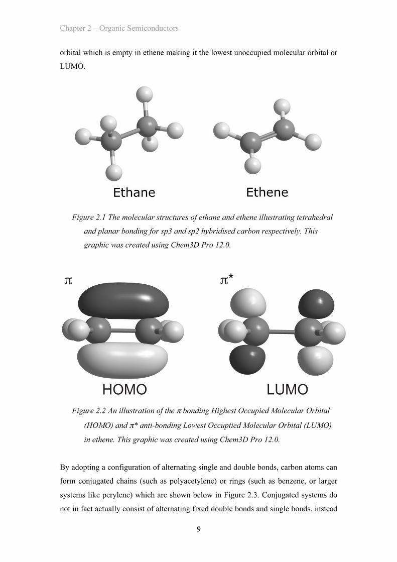
carbon and the planar arrangement of sp2 carbon are illustrated by the 3D diagrams of
ethane and ethene, respectively, in Figure 2.1. An illustration of how the p orbitals
overlap in a π double bond system is shown below in Figure 2.2. When the p orbitals
are in phase a π bond is formed that is filled by the 2 electrons left over from the
single bonds. In ethane this is the highest occupied molecular orbital or HOMO.
When the two p orbitals are out of phase they create a higher energy π* anti-bonding
Chapter 2 – Organic Semiconductors
9
orbital which is empty in ethene making it the lowest unoccupied molecular orbital or
LUMO.
Figure 2.1 The molecular structures of ethane and ethene illustrating tetrahedral
and planar bonding for sp3 and sp2 hybridised carbon respectively. This
graphic was created using Chem3D Pro 12.0.
π*
HOMO LUMO
π
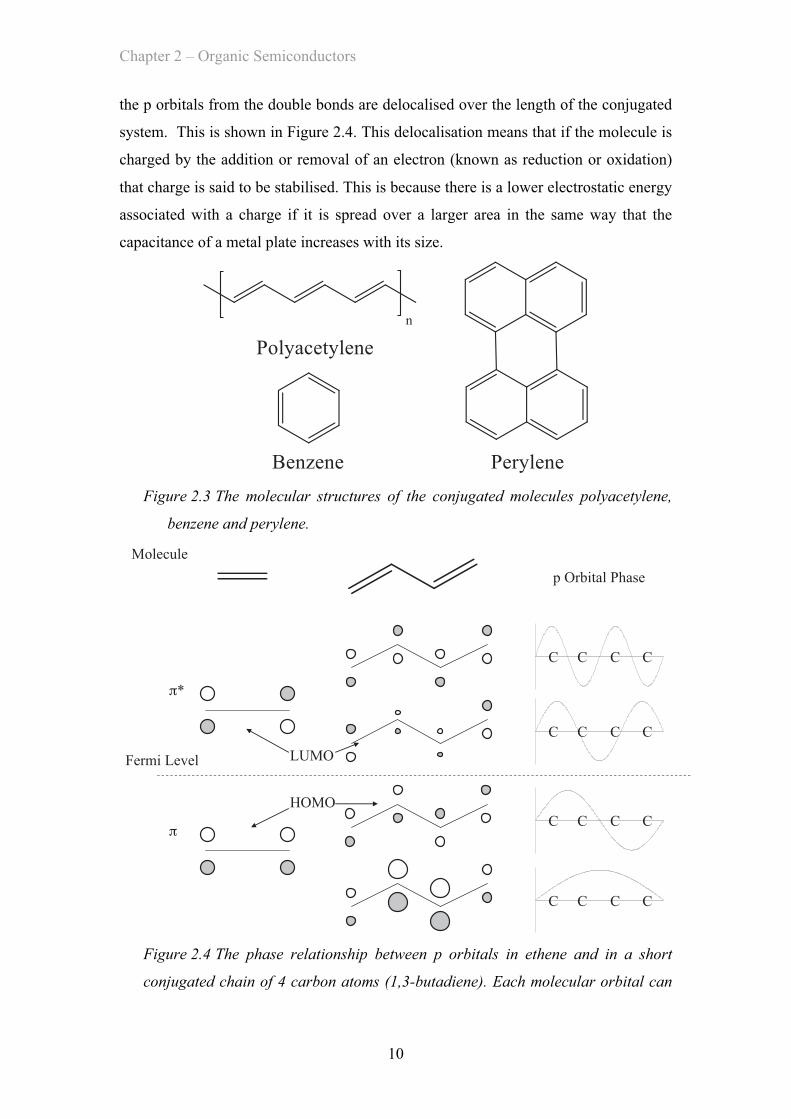
Figure 2.2 An illustration of the π bonding Highest Occupied Molecular Orbital
(HOMO) and π* anti-bonding Lowest Occuptied Molecular Orbital (LUMO)
in ethene. This graphic was created using Chem3D Pro 12.0.
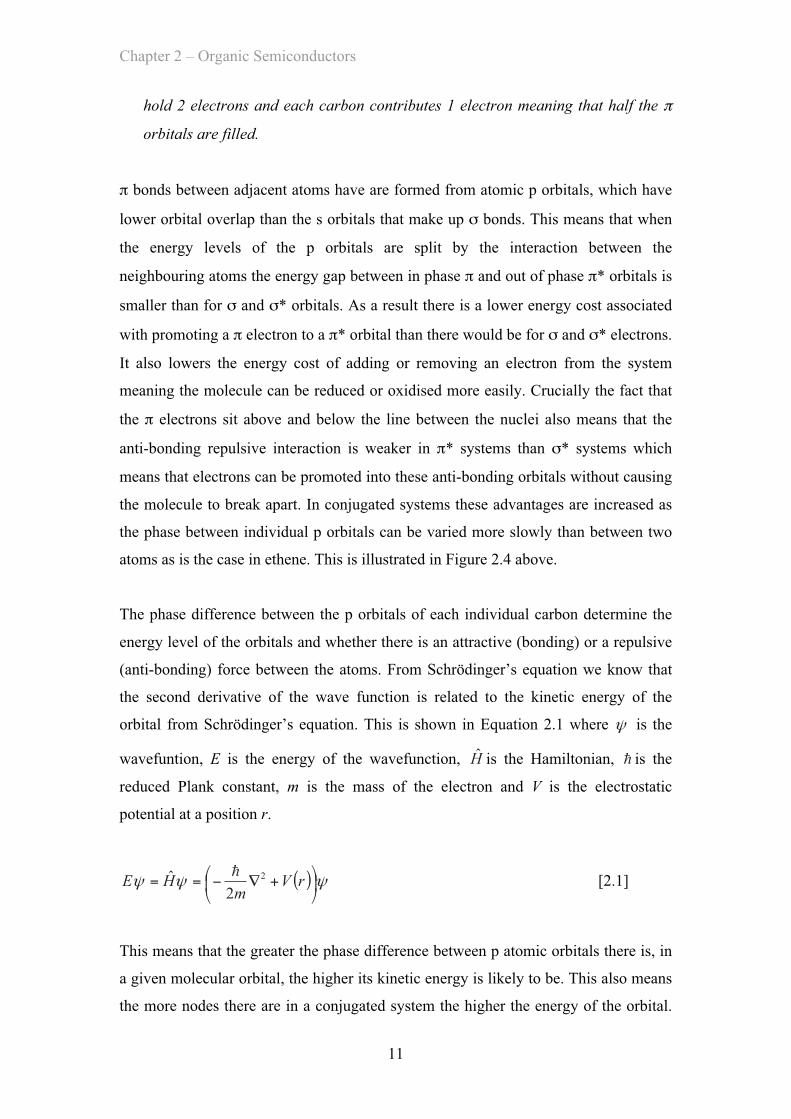
By adopting a configuration of alternating single and double bonds, carbon atoms can
form conjugated chains (such as polyacetylene) or rings (such as benzene, or larger
systems like perylene) which are shown below in Figure 2.3. Conjugated systems do
not in fact actually consist of alternating fixed double bonds and single bonds, instead
Chapter 2 – Organic Semiconductors
10
the p orbitals from the double bonds are delocalised over the length of the conjugated
system. This is shown in Figure 2.4. This delocalisation means that if the molecule is
charged by the addition or removal of an electron (known as reduction or oxidation)
that charge is said to be stabilised. This is because there is a lower electrostatic energy
associated with a charge if it is spread over a larger area in the same way that the
capacitance of a metal plate increases with its size.
Figure 2.3 The molecular structures of the conjugated molecules polyacetylene,
benzene and perylene.
Fermi Level
Molecule
π*
π
p Orbital Phase
-1.1
-0.6
-0.1
0.4
0.9
0 0.3142 0.6284 0.9426 1.2568 1.571 1.8852 2.1994 2.5136 2.8278 3.142
-1.1
-0.6
-0.1
0.4
0.9
0 0.3142 0.6284 0.9426 1.2568 1.571 1.8852 2.1994 2.5136 2.8278 3.142
-1.1
-0.6
-0.1
0.4
0.9
0 0.3142 0.6284 0.9426 1.2568 1.571 1.8852 2.1994 2.5136 2.8278 3.142
-1.1
-0.6
-0.1
0.4
0.9
0 0.3142 0.6284 0.9426 1.2568 1.571 1.8852 2.1994 2.5136 2.8278 3.142C C C C
C C C C
C C C C
C C C C
LUMO
HOMO
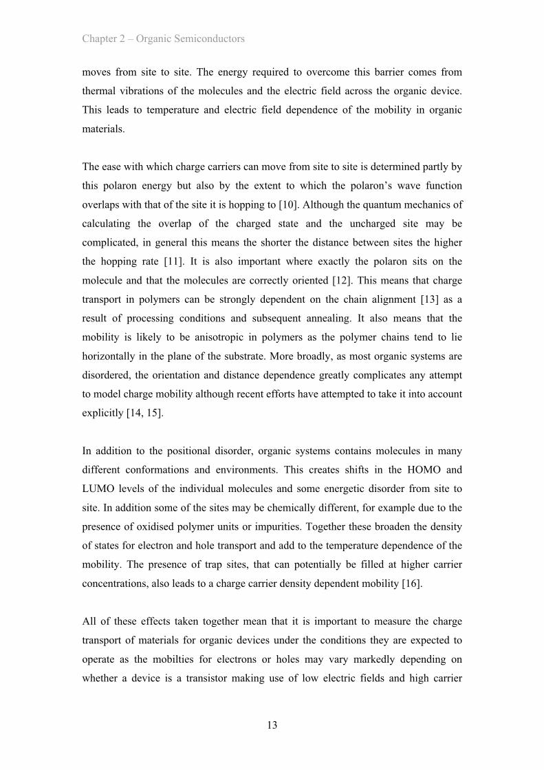
Figure 2.4 The phase relationship between p orbitals in ethene and in a short
conjugated chain of 4 carbon atoms (1,3-butadiene). Each molecular orbital can
Chapter 2 – Organic Semiconductors
11
hold 2 electrons and each carbon contributes 1 electron meaning that half the π
orbitals are filled.
π bonds between adjacent atoms have are formed from atomic p orbitals, which have
lower orbital overlap than the s orbitals that make up σ bonds. This means that when
the energy levels of the p orbitals are split by the interaction between the
neighbouring atoms the energy gap between in phase π and out of phase π* orbitals is
smaller than for σ and σ* orbitals. As a result there is a lower energy cost associated
with promoting a π electron to a π* orbital than there would be for σ and σ* electrons.
It also lowers the energy cost of adding or removing an electron from the system
meaning the molecule can be reduced or oxidised more easily. Crucially the fact that
the π electrons sit above and below the line between the nuclei also means that the
anti-bonding repulsive interaction is weaker in π* systems than σ* systems which
means that electrons can be promoted into these anti-bonding orbitals without causing
the molecule to break apart. In conjugated systems these advantages are increased as
the phase between individual p orbitals can be varied more slowly than between two
atoms as is the case in ethene. This is illustrated in Figure 2.4 above.
The phase difference between the p orbitals of each individual carbon determine the
energy level of the orbitals and whether there is an attractive (bonding) or a repulsive
(anti-bonding) force between the atoms. From Schrödinger’s equation we know that
the second derivative of the wave function is related to the kinetic energy of the
orbital from Schrödinger’s equation. This is shown in Equation 2.1 where ψ is the
wavefuntion, E is the energy of the wavefunction, H is the Hamiltonian, � is the
reduced Plank constant, m is the mass of the electron and V is the electrostatic
potential at a position r.
( ) ψψψ ⎟⎠
⎞⎜⎝
⎛ +∇−== rVm
HE 2
2ˆ �
[2.1]
This means that the greater the phase difference between p atomic orbitals there is, in
a given molecular orbital, the higher its kinetic energy is likely to be. This also means
the more nodes there are in a conjugated system the higher the energy of the orbital.

Chapter 2 – Organic Semiconductors
12
As a node is a point where the wavefunction has opposite phase on either side, these
imply a larger phase difference along the molecule. In addition the nodes in the
wavefunction are regions where there is no electron density as the modulus of the
wavefunction is zero here. With low electron density between the atomic nuclei there
is reduced screening of the positive nuclear charges and less attraction of both nuclei
towards the electron cloud between them. This reduces the attractive interaction
between nuclei and can leave an overall repulsive force resulting in an anti-bonding
orbital.
In conjugated systems, like the one in Figure 2.4, as the length of the conjugated chain
increases the difference in the phases of neighbouring atoms between the HOMO and
the LUMO decreases. This means a smaller band-gap and less repulsive force
between the atoms in the LUMO, making the excited or charged states more stable. In
addition the extended conjugated system stabilises charged states by spreading out the
net charge. Taken together this leads to organic conjugated molecules being able to
act like semiconductors. This was first demonstrated in perylene in 1954 by Hideo
Akamatu et al. [7] and later in polyacetylene in 1977 by Hideki Shirakawa et al. [8].
These researchers found that by doping these molecules with halogens they could
introduce free charge carriers into the materials and increase the conductivity by
several orders of magnitude.
2.4 Charge Transport
Charge transport in organic semiconductors occurs when a molecule in a charged state
transfers its charge to one of its neighbours or when one part of a polymer chain
transfers the charge to the next segment. This charged state is called a polaron after
the distortion introduced in the lattice of a dielectric crystal in response to a charge, an
idea developed by Landau [9]. This distortion occurs as like charged ions in the
structure move away from the free charge and oppositely charge ions to move towards
it. This has the effect of screening the free charge and also reducing the energy of the
charged system. As the energy cost of this distortion must be paid again if the charge
moves this creates a local potential well that must be overcome every time the charge
Chapter 2 – Organic Semiconductors
13
moves from site to site. The energy required to overcome this barrier comes from
thermal vibrations of the molecules and the electric field across the organic device.
This leads to temperature and electric field dependence of the mobility in organic
materials.
The ease with which charge carriers can move from site to site is determined partly by
this polaron energy but also by the extent to which the polaron’s wave function
overlaps with that of the site it is hopping to [10]. Although the quantum mechanics of
calculating the overlap of the charged state and the uncharged site may be
complicated, in general this means the shorter the distance between sites the higher
the hopping rate [11]. It is also important where exactly the polaron sits on the
molecule and that the molecules are correctly oriented [12]. This means that charge
transport in polymers can be strongly dependent on the chain alignment [13] as a
result of processing conditions and subsequent annealing. It also means that the
mobility is likely to be anisotropic in polymers as the polymer chains tend to lie
horizontally in the plane of the substrate. More broadly, as most organic systems are
disordered, the orientation and distance dependence greatly complicates any attempt
to model charge mobility although recent efforts have attempted to take it into account
explicitly [14, 15].
In addition to the positional disorder, organic systems contains molecules in many
different conformations and environments. This creates shifts in the HOMO and
LUMO levels of the individual molecules and some energetic disorder from site to
site. In addition some of the sites may be chemically different, for example due to the
presence of oxidised polymer units or impurities. Together these broaden the density
of states for electron and hole transport and add to the temperature dependence of the
mobility. The presence of trap sites, that can potentially be filled at higher carrier
concentrations, also leads to a charge carrier density dependent mobility [16].
All of these effects taken together mean that it is important to measure the charge
transport of materials for organic devices under the conditions they are expected to
operate as the mobilties for electrons or holes may vary markedly depending on
whether a device is a transistor making use of low electric fields and high carrier
Chapter 2 – Organic Semiconductors
14
densities with charges flowing horizontally, parallel to the substrate, or an LED which
has higher fields and lower charge densities flowing vertically [17].
Typical mobilities in amorphous semiconductor materials, such as those used in
Chapters 6 and 7 in the range of 10-3 to 10-6 cm2/Vs. Highly ordered crystalline
organic semiconductors can reach values of up to 50 cm2/Vs. This is still low
compared to crystalline inorganic semiconductors which have mobilities of about 103
cm2/Vs [18].
2.5 Excited States: Excitons
As was described in Section 2.2, when light is absorbed by a semiconductor
promoting an electron from the conduction to the valance band an electron and a hole
are formed. These charged quasi-particles attract each other electrostatically and can
form a bound state (called an exciton) in which they orbit one another [19, 20]. In
typical inorganic semiconductors the dielectric constant of the material is high and so
the binding energy of the electron hole pair is relatively low, meaning that the initial
photon energy or thermal vibrations can easily dissociate the exciton and form free
charges. Exciton formation in these materials can be seen when the material is excited
below the bandgap energy at low temperatures. As the binding energy reduces the
required photon energy for absorption, “excitonic” absorption bands can be seen in
the region where the photon does not have quite enough energy to cross the bandgap.
When these exictons are formed the high dielectric constant means that the electron
and hole orbit each other at a large radius, several times the lattice spacing. This
means the electrostatic force between the particles can be thought of as resulting from
the averaged lattice and thus the bulk dielectric constant can be used. These excitons
are said to be Mott – Wannier excitons and they have a binding energy simply given
by the binding energy for charges in a dielectric medium. This is similar to the
formula for the energy levels of the hydrogenic atom in free space and is given below
in Equation 2.2. Where bindingE is the exciton binding energy, e is the electronic
charge, *m is the reduced effective mass of the electron-hole system, h is Planck’s
Chapter 2 – Organic Semiconductors
15
constant, ε is the dielectric constant and n is an integer which represents the various
possible allowed exciton orbital states.
222
4
2
*
nhme
Ebinding ε= [2.2]
In materials with lower dielectric constants the exciton radius is smaller due to the
higher binding energy and so the crystal lattice cannot simply be averaged over and
this simple model cannot be used. These are referred to as Poole - Frenkel excitons.
Organic semiconductors have low dielectric constants and they are not extended
systems with periodic lattices. This means that the emissive state is not free electron
holes recombining but localised excitons. Their excitations are related to the
molecular orbitals described more fully in Section 2.3. The exciton is not well
described as an electron and hole orbiting each other but instead as an excited state of
the entire molecule. A third intermediate type of excition exists in donor-acceptor
molecular blends, like those used in organic photovoltaics, called a charge transfer
(CT) exciton. CT excitons are delocalised across a pair of donor acceptor molecules.
When the light is first absorbed it can be thought of as an instantaneous transition
from the HOMO to the LUMO of the molecule. However once the molecule is
excited, the nuclei will relax in a manner similar to a polaron described in Section 2.5
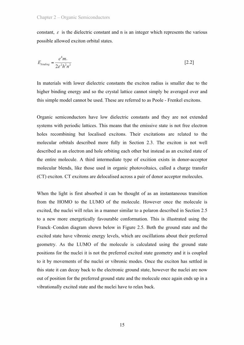
to a new more energetically favourable conformation. This is illustrated using the
Franck–Condon diagram shown below in Figure 2.5. Both the ground state and the
excited state have vibronic energy levels, which are oscillations about their preferred
geometry. As the LUMO of the molecule is calculated using the ground state
positions for the nuclei it is not the preferred excited state geometry and it is coupled
to it by movements of the nuclei or vibronic modes. Once the exciton has settled in
this state it can decay back to the electronic ground state, however the nuclei are now
out of position for the preferred ground state and the molecule once again ends up in a
vibrationally excited state and the nuclei have to relax back.
Chapter 2 – Organic Semiconductors
16
Ene
rgy
Nuclear Coordinates
Excited State
Ground State
VibronicLevels
Absorption Radiative/ Non RadiativeDecay
VibronicRelaxation
VibronicRelaxation
Figure 2.5 The Frank-Condon diagram illustrating the vibronic modes of the
ground and excited electronic states and the transitions between them.
The result of these molecular relaxations is that the energy of the emitted light from
an organic semiconductor will be lower than the excitation energy from absorbed
photons. The difference between the optical absorption of a material and its emission
is known as its Stokes shift.
2.6 Organic Semiconductors for Devices
Organic semiconductors have a band gap energy that naturally lies close to the visible
part of the spectrum. For this reason organic molecules have long been used as dyes.
An example of an organic dye is porphyrin which derives its name from the Greek
word for purple and in the form of the iron complex haem is responsible for the colour
of red blood cells. The black colour of coal and pencils comes from extended
conjugated graphene type systems which have a small enough band gap that they
efficiently absorb right across the visible spectrum. The favourable band gap energy
of organic semiconductors combined with strong dipole moments, which allow

Chapter 2 – Organic Semiconductors
17
efficient coupling to light, make them attractive materials for applications involved in
inter-converting light and electricity, also known as optoelectronics.
Another key advantage of organic semiconductors is that they can be readily
functionalised or modified using the wide range of techniques available from
synthetic organic chemistry. This allows excellent control over light-emitting and
physical properties by modifying the structure of the molecules to suit the needs of the
application. Organic synthetic techniques can produce the desired materials in large
quantities. In addition organic materials do not require carefully grown defect free
crystals that are commonly used in inorganic semiconductors. Large quantities of the
material can easily be produced and stored without the final substrate even being in
sight allowing the construction of separate facilities for synthesis and device
fabrication.
Finally some organic molecules can be readily dissolved in organic solvents, which in
addition to being a boon for organic chemists, allows easy processing of materials.
The semiconductor can be dissolved in a volatile solution and coated by spin casting,
doctor blading or even ink-jet printing [21] in a manner that is far lower cost than
sophisticated chemical vapour deposition or molecular beam epitaxy techniques
required for growing inorganic semiconductor crystals. The fabrication of entire
arrays of light-emitting diodes to form a single display of usable size [22] become
possible via ink-jet printing in a way that wouldn’t be economical for inorganic
devices. Solution-processing also allows compatibility with a wider range of
substrates, which together with the flexibility of organics allows fully flexible
electronic devices [22].
Not all organic molecules are soluble in common solvents or suitable for solution
processing. Today much work is done using organic molecules that are only sparingly
soluble in most solvents and do not form good films when spin cast. These small
molecules tend to be deposited by thermal evaporation in high vacuum which is a
relatively high cost processing technique. Small molecules have also been used to
form high purity single crystals however the slow growth of these crystals means that
they are not really suited for solution-processing on a large scale. The majority of
solution processable organic semiconductors take the form of much higher molecular
Chapter 2 – Organic Semiconductors
18
weight polymers and oligomers, however solution processible dendrimers have also
been developed. These molecules use a small molecule core surrounded by dendron
arms which help protect the core from quenching interactions with its neighbours and
help solubilise it. They are discussed in detail in Chapter 3.
Organic semiconductors have been successfully used in a wide range of
semiconductor devices including transistors [23, 24], light-emitting diodes [25, 26],
solar cells [27, 28] and lasers [29]. Organic transistors, LEDs and solar cells are now
being produced commercially and organic lasers are now efficient and compact
enough to be pumped by a single inorganic LED [30]. Organic light-emitting diodes
are described in detail in chapter 3 but a basic overview of the other devices is given
below.
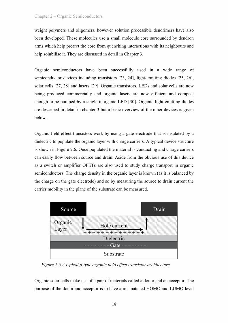
Organic field effect transistors work by using a gate electrode that is insulated by a
dielectric to populate the organic layer with charge carriers. A typical device structure
is shown in Figure 2.6. Once populated the material is conducting and charge carriers
can easily flow between source and drain. Aside from the obvious use of this device
as a switch or amplifier OFETs are also used to study charge transport in organic
semiconductors. The charge density in the organic layer is known (as it is balanced by
the charge on the gate electrode) and so by measuring the source to drain current the
carrier mobility in the plane of the substrate can be measured.
Substrate
- - - - - - - - Gate - - - - - - - -Dielectric
Hole current
Source Drain
+ + + + + + + + + + + + + +
OrganicLayer
Figure 2.6 A typical p-type organic field effect transistor architecture.
Organic solar cells make use of a pair of materials called a donor and an acceptor. The
purpose of the donor and acceptor is to have a mismatched HOMO and LUMO level

Chapter 2 – Organic Semiconductors
19
to split the excitons resulting from the absorbed phonons. The excited electron will
transfer to the material with the lower LUMO (the acceptor) and the resulting hole
will transfer to the material with the higher HOMO level (the donor). This is shown in
Figure 2.7(a). An advantage of solution-processed organic semiconductors is that they
can interpenetrate one another creating a bulk hetrojunction with a larger surface area,
where excitons can be split, compared to evaporated organic devices. A typical device
structure is shown in Figure 2.7(b).
Donor Acceptor
+
-
CathodeAnode
Electron
Hole
LUMO
HOMO
A
Ele
ctro
n E
nerg
y
B
Anode
Cathode
Donor
Acceptor
Figure 2.7 The band structure (a) and device structure (b) of a typical bulk
hetrojunction organic solar cell
The key requirement for lasing is a material that can produce optical gain. This is
achieved in a laser through stimulated emission, when a photon passing through the
medium increases the rate at which other photons of the same wavelength are emitted.
In a two level system the molecules that are unexcited will also absorb light at this
wavelength thereby attenuating the light. This means that unless more molecules are
in the excited state and ready to emit than are in the final state and ready to absorb the
light, the material will not provide gain. This required distribution of molecular states
is called a population inversion and cannot be achieved in a two level system.
Fortunately, as shown in Figure 2.5, the vibronic relaxations of the excited state and
ground state after transistions create a four level system in organic semiconductors
and thus gain is possible. This allows the creation of optical amplifiers [31] and, by
using a light pulse to depopulate the emissive level for short periods of time, optical
switches [32].
Chapter 2 – Organic Semiconductors
20
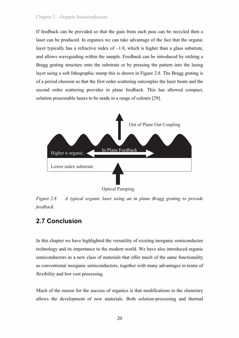
If feedback can be provided so that the gain from each pass can be recycled then a
laser can be produced. In organics we can take advantage of the fact that the organic
layer typically has a refractive index of ~1.8, which is higher than a glass substrate,
and allows waveguiding within the sample. Feedback can be introduced by etching a
Bragg grating structure onto the substrate or by pressing the pattern into the lasing
layer using a soft lithographic stamp this is shown in Figure 2.8. The Bragg grating is
of a period choosen so that the first order scattering outcouples the laser beam and the
second order scattering provides in plane feedback. This has allowed compact,
solution processable lasers to be made in a range of colours [29].
In Plane Feedback
Out of Plane Out Coupling
Lower index substrate
Higher n organic
Optical Pumping
Figure 2.8 A typical organic laser using an in plane Bragg grating to provide
feedback.
2.7 Conclusion
In this chapter we have highlighted the versatility of existing inorganic semiconductor
technology and its importance to the modern world. We have also introduced organic
semiconductors as a new class of materials that offer much of the same functionality
as conventional inorganic semiconductors, together with many advantages in terms of
flexibility and low cost processing.
Much of the reason for the success of organics is that modifications to the chemistry
allows the development of new materials. Both solution-processing and thermal
Chapter 2 – Organic Semiconductors
21
evaporation allow emissive guests to be blended with charge transport hosts for
greater OLED efficiency or acceptors to be blended with donors for efficient charge
separation in solar cells. In polymers solar cells, for example, much attention is also
paid to phase separation and ways to control it by varying solvent mixture and thermal
annealing regimes.
This flexibility, combined with ease of solution-processing means that organic
electronics is an area that is likely to have many commercial applications.
1. Brattain, W.H. and J. Bardeen, The Transistor, A Semi-Conductor Triode. Physics Review, 1948. 74: p. 230.
2. Mahan, G.D., Good thermoelectrics, in Solid State Physics, Vol 511998, Academic Press Inc: San Diego. p. 81-157.
3. Seebeck, T.J., Ueber die magnetische Polarisation der Metalle und Erze durch Temperatur-Differenz. Annalen der Physik, 1826. 82(2): p. 160.
4. Chapin, D.M., C.S. Fuller, and G.L. Pearson, A New Silicon p-n Junction Photocell for Converting Solar Radiation into Electrical Power. 1954. 25(5): p. 677.
5. Holonyak, J.N. and S.F. Bevacqua, Coherent (Visible) Light Emission From Ga(As 1 - x P x ) Junctions. Applied Physics Letters, 1962. 1(4): p. 83.
6. Genoe, J., et al., pnp Resonant Tunneling Light-Emitting Transistor. Applied Physics Letters, 1992. 61(9): p. 1051-1053.
7. Akamatu, H., H. Nokuchi, and Y. Matsunga, Electrical Conductivity of the Perylene–Bromine Complex. Nature, 1954. 173: p. 168.
8. Shirakawa, H., et al., Sythesis of Electically Conducting Organic Polymers - Halogen Derivatives of Polyacetylene, (CH)x. Journal of the Chemical Society-Chemical Communications, 1977(16): p. 578-580.
9. Landau, L.D., On the motion of electrons in a crystal lattice'. Phys. Z. Sowjetunion, 1933. 3: p. 884.
10. Bredas, J.L., et al., Organic semiconductors: A theoretical characterization of the basic parameters governing charge transport. Proceedings of the National Academy of Sciences of the United States of America, 2002. 99(9): p. 5804-5809.
11. Markham, J.P.J., et al., Charge transport in highly efficient iridium cored electrophosphorescent dendrimers. Journal of Applied Physics, 2004. 95(2): p. 438-445.
12. Yamada, T., et al., Revealing bipolar charge-transport property of 4,4′-N,N′-dicarbazolylbiphenyl (CBP) by quantum chemical calculations. Organic Electronics, 2011. 12(1): p. 178.
13. Sirringhaus, H., et al., Two-dimensional charge transport in self-organized, high-mobility conjugated polymers. Nature, 1999. 401(6754): p. 685-688.
14. Vukmirovic, N. and L.W. Wang, Carrier hopping in disordered semiconducting polymers: How accurate is the Miller-Abrahams model? Applied Physics Letters, 2010. 97(4): p. 043305.
Chapter 2 – Organic Semiconductors
22
15. MacKenzie, R.C.I., J.M. Frost, and J. Nelson, A numerical study of mobility in thin films of fullerene derivatives. Journal of Chemical Physics, 2010. 132(6): p. 064904.
16. Tanase, C., et al., Charge carrier density dependence of the hole mobility in poly(p-phenylene vinylene). Physica Status Solidi a-Applied Research, 2004. 201(6): p. 1236-1245.
17. Tanase, C., et al., Unification of the hole transport in polymeric field-effect transistors and light-emitting diodes. Physical Review Letters, 2003. 91(21): p. 216601.
18. Coropceanu, V., et al., Charge transport in organic semiconductors. Chemical Reviews, 2007. 107(4): p. 926-952.
19. Liang, W.Y., Excitons Physics Education 1970. 4: p. 226. 20. Wannier, G.H., The Structure of Electronic Excitation Levels in Insulating
Crystals. Physics Review, 1937. 52(3). 21. Forrest, S.R., The path to ubiquitous and low-cost organic electronic
appliances on plastic. Nature, 2004. 428: p. 911. 22. Zhou, L.S., et al., All-organic active matrix flexible display. Applied Physics
Letters, 2006. 88(8): p. 083502. 23. Newman, C.R., et al., Introduction to organic thin film transistors and design
of n-channel organic semiconductors. Chemistry of Materials, 2004. 16(23): p. 4436-4451.
24. Sirringhaus, H., Device physics of Solution-processed organic field-effect transistors. Advanced Materials, 2005. 17(20): p. 2411-2425.
25. Geffroy, B., P. Le Roy, and C. Prat, Organic light-emitting diode (OLED) technology: materials, devices and display technologies. Polymer International, 2006. 55(6): p. 572-582.
26. Grimsdale, A.C., et al., Synthesis of Light-Emitting Conjugated Polymers for Applications in Electroluminescent Devices. Chemical Reviews, 2009. 109(3): p. 897-1091.
27. Spanggaard, H. and F.C. Krebs, A brief history of the development of organic and polymeric photovoltaics. Solar Energy Materials and Solar Cells, 2004. 83(2-3): p. 125-146.
28. Scharber, M.C., et al., Design rules for donors in bulk-heterojunction solar cells - Towards 10 % energy-conversion efficiency. Advanced Materials, 2006. 18(6): p. 789.
29. Samuel, I.D.W. and G.A. Turnbull, Organic semiconductor lasers. Chemical Reviews, 2007. 107(4): p. 1272-1295.
30. Yang, Y., G.A. Turnbull, and I.D.W. Samuel, Hybrid optoelectronics: A polymer laser pumped by a nitride light-emitting diode. Applied Physics Letters, 2008. 92(16): p. 163306.
31. Amarasinghe, D., et al., Broadband solid state optical amplifier based on a semiconducting polymer. Applied Physics Letters, 2006. 89(20): p. 201119.
32. Amarasinghe, D., et al., Picosecond gain switching of an organic semiconductor optical amplifier. Applied Physics Letters, 2008. 92(8): p. 083305.
23
3. Organic Light Emitting Diodes
3.1 Introduction ............................................................................................................ 23�3.1.2 OLEDs vs. LCD Displays ........................................................................... 24�3.1.3 OLEDs for Lighting .................................................................................... 26�
3.2 Characterising OLEDs: Device Parameters ........................................................... 26�3.2.1 Power Efficiency ......................................................................................... 26�3.2.2 Brightness ................................................................................................... 27�3.2.3 CIE Colour Co-ordinates ............................................................................ 28�3.2.4 Colour Rendering Index .............................................................................. 30�3.2.5 External Quantum Efficiency and Luminous Efficiency ............................ 31�3.2.6 Lifetime ....................................................................................................... 31�
3.3 Light Emission In OLEDs ..................................................................................... 32�3.4 Materials for OLED devices .................................................................................. 35�
3.4.1 Host-Guest Blending ................................................................................... 36�3.4.2 Phosphorescent Emitters ............................................................................. 36�3.4.3 Aggregated States: Dimers and Excimers ................................................... 43�
3.4 Design of OLEDs ................................................................................................... 46�3.4.1 Charge Injection .......................................................................................... 46�3.4.2 Electrode Quenching ................................................................................... 48�3.4.3 Charge Transport Layers ............................................................................. 48�3.4.4 Light Extraction .......................................................................................... 50�
3.1 Introduction
In the previous chapter on organic electronics I discussed the basics of light emission
and charge transport in organic materials. By placing a thin ~100 nm layer of an
emissive, semiconducting material between two electrodes we can electrically excite
its luminescence and create an Organic Light Emitting Diode (OLED) [1]. Like their
inorganic LED counterparts, OLEDs have significant practical applications. At
present OLEDs are being developed commercially and have been deployed to replace
Chapter 3 – Organic Light Emitting Diodes
24
liquid crystal displays in mobile phones, cameras and televisions. The first OLEDs for
lighting products are available commercially and in the near future are likely to offer
an alternative to fluorescent and halogen lights.
In Section 3.2, I will discuss how to characterise an OLED and determine its fitness
for display and lighting applications. In Section 3.3 I will introduce an overview of
light emission in OLEDs and the parameters that result in good OLED efficiency. The
development of materials for OLEDs is discussed in Section 3.4 and the design of
OLED device structures is covered in Section 3.5.
3.1.2 OLEDs vs. LCD Displays
The main flat screen display technology in use at the moment is the liquid crystal
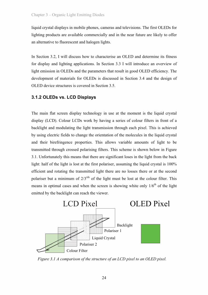
display (LCD). Colour LCDs work by having a series of colour filters in front of a
backlight and modulating the light transmission through each pixel. This is achieved
by using electric fields to change the orientation of the molecules in the liquid crystal
and their birefringence properties. This allows variable amounts of light to be
transmitted through crossed polarising filters. This scheme is shown below in Figure
3.1. Unfortunately this means that there are significant loses in the light from the back
light: half of the light is lost at the first polariser, assuming the liquid crystal is 100%
efficient and rotating the transmitted light there are no losses there or at the second
polariser but a minimum of 2/3rds of the light must be lost at the colour filter. This
means in optimal cases and when the screen is showing white only 1/6th of the light
emitted by the backlight can reach the viewer.
LCD Pixel OLED Pixel
Backlight
Polariser 1
Liquid Crystal
Polariser 2
Colour Filter
Figure 3.1 A comparison of the structure of an LCD pixel to an OLED pixel.
Chapter 3 – Organic Light Emitting Diodes
25
In addition if a white (rather than narrow line width red, green and blue LED)
backlight is used the narrower the colour filters, and greater the colour purity, the
more light is lost. This makes LCD displays intrinsically less bright and more limited
in their colour purity than OLED displays which control the brightness of the pixel
directly.
The LCD system is thick and this limits the possible viewing angle and takes up space
in compact devices. By contrast the OLED device can be less than a micron thick and
so has no viewing angle issues. Finally when showing blacks the LCD display is
wasting the backlight power as it simply shutters off the backlight. This process is
also imperfect allowing some light to leak through and limiting the contrast ratio.
OLEDs are off when the pixels are not required, saving power and giving better
contrast ratios. OLEDs can achieve ratios of 1,000,000:1 compared in the dark to only
10,000:1 for LCDs and commercial LCD displays can have a ratio less than 1,000:1.
Contrast ratios for OLED screens in practice are limited mostly by reflected light [2].
Performing well when showing black is a significant advantage when viewing movies
as darkness and shadow are often used to provide drama in cinema releases. It is less
important when viewing text, which tends to be black on white.
Another advantage of OLEDs over LCDs is that the liquid crystal can take time to re-
orient in response to the applied field. This can lead to response times of 15-25
milliseconds per frame. OLEDs can be turned on and off much faster than this and
have been pulsed as quickly as ~100 ns [3]. In practice the fastest switching speed is
determined by the capacitances in the pixel and the speed at which the pixels can be
addressed. In any case this allows faster refresh rates with OLED displays for high
performance applications where motion tracking is important, for example in
computer games or watching sport.
Finally OLEDs and organic transistors are compatible with flexible substrates
allowing flexible displays. This might allow concepts such as flexible “e-paper” but
also means that the devices are less vulnerable to sudden impacts than rigid LCD
displays. These are both features that are attractive for portable applications.
Chapter 3 – Organic Light Emitting Diodes
26
3.1.3 OLEDs for Lighting
White OLEDs have advantages over fluorescent lighting in power efficiency [4] and
producing more aesthetically pleasing orange “warm” white colours [5, 6] (see section
3.2 below). They also have the advantage that they are available in thin layers that
provide an even light over a large area. This in particular reduces glare and so does
not require luminaires or light fittings to provide uniform illumination. This means the
light fittings require less space and avoid efficiency losses associated with luminaires.
These panels could even be flexible conforming to curved surfaces allowing more
choices to architects or making it easier to fit lighting to vehicle interiors. The large
OLED lighting panels move in the opposite direction to inorganic LED lighting which
uses expensive chips driven at very high brightnesses, due to their high cost of
fabrication per unit area, increasing glare and the requirement for luminaires.
3.2 Characterising OLEDs: Device Parameters
An overview of the parameters on which OLEDs are assessed is given here, while the
experimental details of the determination of the various device parameters are given
in Chapter 4.
3.2.1 Power Efficiency
The simplest device parameter to understand is power efficiency. Clearly for any
given application it is better if a given amount of light can be produced for the
smallest possible amount of electrical power.
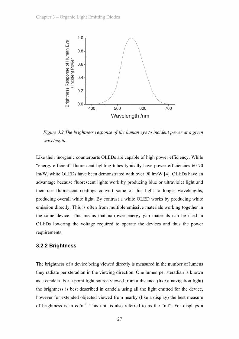
When calculating the useful amount of light put out by a light source we cannot
simply measure its output in Watts because the human eye is not equally sensitive to
all wavelengths (as shown in Figure 3.2). We instead need a new unit that measures
the amount of useful light based on the eye’s perceptions. This perceived brightness is
measured in lumens or lm and so the power efficiency is measured in lumens per Watt
or lm/W of electrical power.
Chapter 3 – Organic Light Emitting Diodes
27
400 500 600 7000.0
0.2
0.4
0.6
0.8
1.0
Bri
gh
tne
ss R
esp
on
se
of
Hu
ma
n E
ye
/ In
cid
en
t P
ow
er
Wavelength /nm
Figure 3.2 The brightness response of the human eye to incident power at a given
wavelength.
Like their inorganic counterparts OLEDs are capable of high power efficiency. While
“energy efficient” fluorescent lighting tubes typically have power efficiencies 60-70
lm/W, white OLEDs have been demonstrated with over 90 lm/W [4]. OLEDs have an
advantage because fluorescent lights work by producing blue or ultraviolet light and
then use fluorescent coatings convert some of this light to longer wavelengths,
producing overall white light. By contrast a white OLED works by producing white
emission directly. This is often from multiple emissive materials working together in
the same device. This means that narrower energy gap materials can be used in
OLEDs lowering the voltage required to operate the devices and thus the power
requirements.
3.2.2 Brightness
The brightness of a device being viewed directly is measured in the number of lumens
they radiate per steradian in the viewing direction. One lumen per steradian is known
as a candela. For a point light source viewed from a distance (like a navigation light)
the brightness is best described in candela using all the light emitted for the device,
however for extended objected viewed from nearby (like a display) the best measure
of brightness is in cd/m2. This unit is also referred to as the “nit”. For displays a
Chapter 3 – Organic Light Emitting Diodes
28
brightness of 200-300 cd/m2 is a typical maximum brightness and 100 cd/m2 is typical
of normal usage and so it is best to assess the performance of OLEDs for displays at
this brightness.
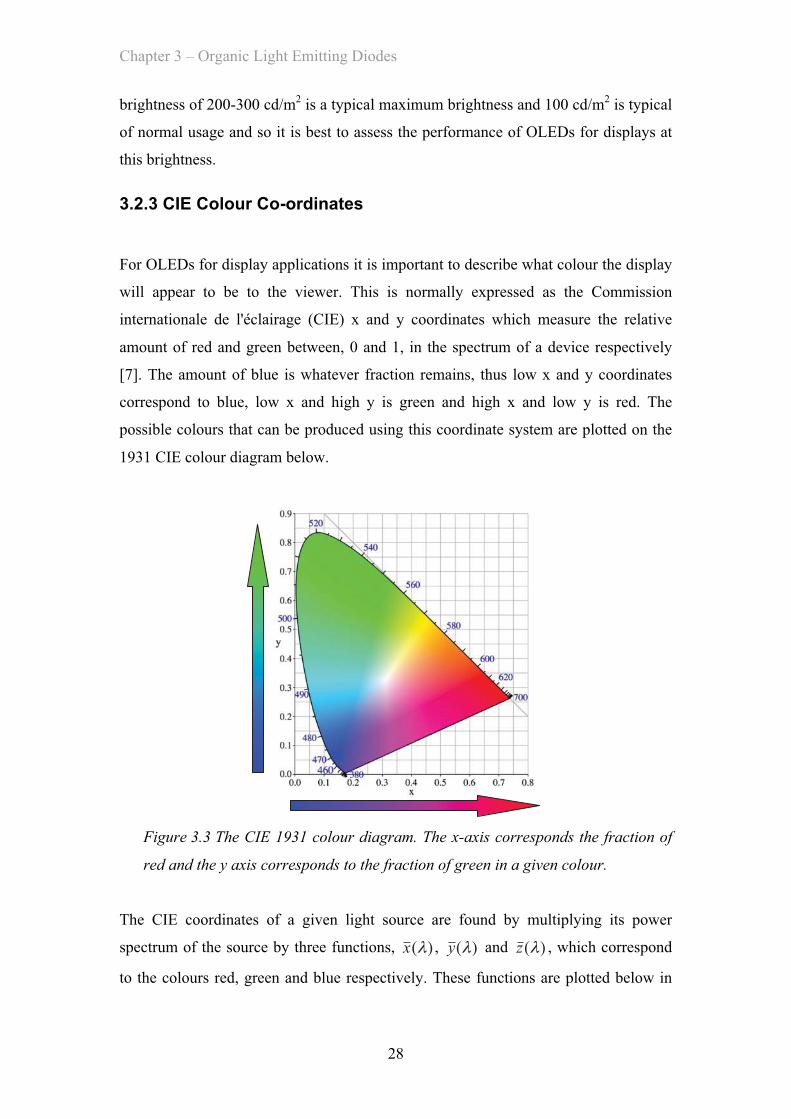
3.2.3 CIE Colour Co-ordinates
For OLEDs for display applications it is important to describe what colour the display
will appear to be to the viewer. This is normally expressed as the Commission
internationale de l'éclairage (CIE) x and y coordinates which measure the relative
amount of red and green between, 0 and 1, in the spectrum of a device respectively
[7]. The amount of blue is whatever fraction remains, thus low x and y coordinates
correspond to blue, low x and high y is green and high x and low y is red. The
possible colours that can be produced using this coordinate system are plotted on the
1931 CIE colour diagram below.
Figure 3.3 The CIE 1931 colour diagram. The x-axis corresponds the fraction of
red and the y axis corresponds to the fraction of green in a given colour.
The CIE coordinates of a given light source are found by multiplying its power
spectrum of the source by three functions, )(λx , )(λy and )(λz , which correspond
to the colours red, green and blue respectively. These functions are plotted below in
Chapter 3 – Organic Light Emitting Diodes
29
Figure 3.4. The green response )(λy also happens to correspond the eye’s brightness
response described above in Section 3.2.1.
400 500 600 7000.0
0.5
1.0
1.5
2.0
Re
lative
Re
sp
on
se
/In
cid
en
t P
ow
er
Wavelength /nm
Figure 3.4 The CIE 1931 colour matching functions )(λx (dashed blue line),
)(λy (thick green line) and )(λz (thin red line).
Using the )(λx , )(λy and )(λz functions the amounts of red (X), green (Y) and blue
(Z) can be determined using the integrals 3.1, 3.2 and 3.3 below. Here ( )λβ is the
emission spectrum in units of photons per unit wavelength that has been converted
into the power per unit wavelength by dividing by the wavelengthλ .
∫= λλ
λβλ dxX )()( [3.1]
∫= λλ
λβλ dyY )()( [3.2]
∫= λλ
λβλ dzZ )()( [3.3]
Ignoring the brightness of the source the fraction of green and red response gives the
CIE x and y coordinates respectively using Equations [3.4] and [3.5] below. This
allows the colour of the OLED to be plotted on the CIE colour diagram shown in
Figure 3.3.
Chapter 3 – Organic Light Emitting Diodes
30
ZYXXx++
= [3.4]
ZYXYy++
= [3.5]
For colour displays pixels should have the most saturated possible colours possible so
that they can be used in combination to show the widest possible array of colours. It
has been a challenge to produce deep blue emitting devices because it can be difficult
to find suitably high energy band gap materials [8, 9]. This means achieving pure blue
emission, as well as high efficiency is a key requirement for OLEDs for displays.
3.2.4 Colour Rendering Index
The faithfulness with which colours are reproduced when illuminated by a light
source is measured by a number called the colour rendering index or CRI. A value of
100 is the best possible CRI and corresponds to a reference good quality white source.
A light which does not have even light emission across the visible may appear white
when looking directly at it while still being not be useful for trying to illuminate
coloured objects because parts of the objects reflection spectrum can fall into gaps in
the emission spectrum of the light source. For displays and signs the colour rendering
index is not important as the devices will not be used to illuminate objects but are
designed to be viewed directly.
The phosphors for down conversion in fluorescent lights often give imperfect white
emission and don’t evenly cover the spectrum. OLEDs typically use materials with
relatively broad emission spectra giving a more even coverage. The phosphors can
also let though a relatively large amount of blue light leading to “cold” white light
which can be less aesthetically pleasing than the “warm” emission that is more
weighted towards the red from black body emitters like older incandescent light bulbs
or the sun. As OLEDs do not rely on these phosphors it is easier to modify their
emission to give a more pleasing neutral or warm orange white. One way of
quantifying this factor is to try to fit the spectrum to that of the nearest black body
spectrum to give a “colour temperature” for the light source in Kelvin. Ironically this
Chapter 3 – Organic Light Emitting Diodes
31
means that “cool” bluish emission is assigned a high colour temperature (often over
10,000 K) and “warm” reddish light is assigned a lower temperature (say 3,000 K)!
3.2.5 External Quantum Efficiency and Luminous Efficiency
For research applications another companion to power efficiency is external quantum
efficiency, which is the number of photons that are emitted from the device per
electron passed through it. As is noted later in Section 3.4.4 not all photons escape
from the device and so if a calculation is performed to find how many photons were
created within the device we can find the internal quantum efficiency.
External quantum efficiency is a parameter that is useful in a research context but is
not directly valuable in a finished device. While power efficiency can be improved by
reducing drive voltage by optimising device thicknesses, cathode and anode materials
and by choosing high mobility host materials (all of which are discussed further on in
this chapter) external quantum efficiency provides a measure of how efficient a
material can be in a device context before this optimisation has been done and so it is
a measure of the material’s promise. Luminous efficiency per unit current (measured
in cd/A) is a closely related parameter. For a given emission spectrum or colour of
device these numbers are related by a simple ratio determined by the human eye’s
sensitivity to that colour. This means that luminous efficiency values are highest for
green devices and lower for red and blue devices for a given external quantum
efficiency.
3.2.6 Lifetime
Another important parameter for practical devices is the lifetime. The time that a
device can function at a given initial brightness before its brightness has dropped to
80% or 50% without changing the drive conditions is the T80 or T50 lifetime. The
lifetime of OLEDs is affected by the choice of materials used but as these are
degraded by the leakage of oxygen or water into the device the technology used to
encapsulate the devices is very important. In addition longer lifetimes can be achieved
by avoiding the use of reactive metals in the devices as the cathodes. Currently
lifetimes for OLED displays and lighting panels used commercially are rated to
Chapter 3 – Organic Light Emitting Diodes
32
exceed 10,000 hours of continuous use and some exceed 100,000 hours. In practice
these tests are done using accelerated aging techniques to model performance.
3.3 Light Emission In OLEDs
In order to be a suitable choice of material for use in the emissive layer of an OLED a
material must first be an efficient light emitter. This is measured by seeing what
fraction of excitations of a molecule result in the emission of a photon and what
fraction decay non-radiatively. If an optical excitation is used this number is called the
photoluminescence quantum yield or PLQY (Φ ) [10, 11].
Provided the electron and hole recombine to form a singlet exciton there is no
difference between optically excited molecules and electrically excited molecules and
so the PLQY is a relevant parameter for choosing which materials are suitable for use
in OLEDs. Unfortunately ~75% of electrons and holes will instead recombine to form
a triplet exciton, which is non-emissive in ordinary fluorescent emitters. Some
materials, known as phosphorescent emitters, also allow emission from the triplet
excitons. This effect is discussed in detail in Chapter 6, which concerns
phosphorescent polymers. In this chapter the ratio of singlet to total excitons formed
is expressed as spinη .
For electrical current through an OLED to produce light, electrons and holes must
recombine rather than simply passing all the way through the device from one side to
the other. In the best organic devices careful device design means that close to 100%
of charge carriers recombine effectively. This recombination or capture fraction
is captureη .
Finally any light emitted by the emissive material must find a way to leave the device.
Unfortunately solids have higher refractive indexes than air and this leads to a
situation where emitted light can be trapped in waveguided modes inside the device.
Organic semiconductors typically have a refractive index of about 1.6-1.8 [12-14]
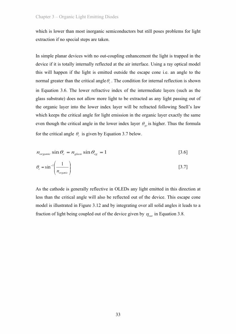
Chapter 3 – Organic Light Emitting Diodes
33
which is lower than most inorganic semiconductors but still poses problems for light
extraction if no special steps are taken.
In simple planar devices with no out-coupling enhancement the light is trapped in the
device if it is totally internally reflected at the air interface. Using a ray optical model
this will happen if the light is emitted outside the escape cone i.e. an angle to the
normal greater than the critical angle cθ . The condition for internal reflection is shown
in Equation 3.6. The lower refractive index of the intermediate layers (such as the
glass substrate) does not allow more light to be extracted as any light passing out of
the organic layer into the lower index layer will be refracted following Snell’s law
which keeps the critical angle for light emission in the organic layer exactly the same
even though the critical angle in the lower index layer gcθ is higher. Thus the formula
for the critical angle cθ is given by Equation 3.7 below.
1sinsin == cgglasscorganic nn θθ [3.6]
⎟⎟⎠
⎞⎜⎜⎝
⎛= −
organicc n
1sin 1θ [3.7]
As the cathode is generally reflective in OLEDs any light emitted in this direction at
less than the critical angle will also be reflected out of the device. This escape cone
model is illustrated in Figure 3.12 and by integrating over all solid angles it leads to a
fraction of light being coupled out of the device given by outη in Equation 3.8.
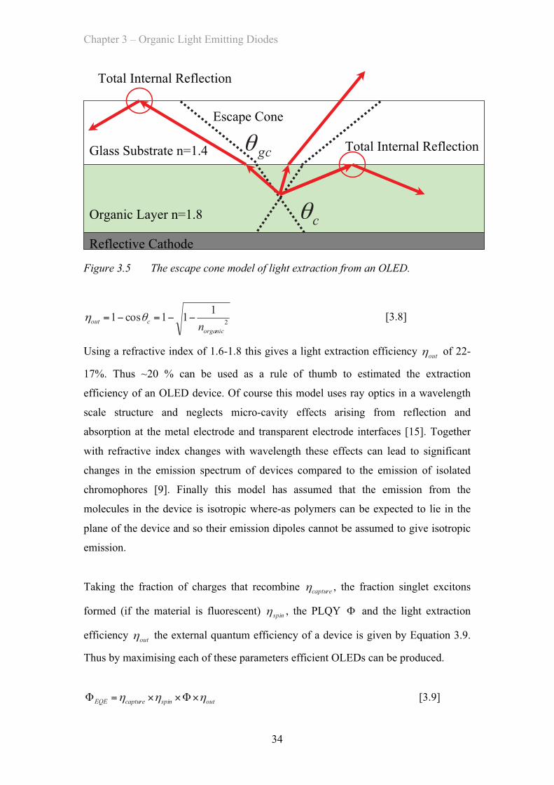
Chapter 3 – Organic Light Emitting Diodes
34
Escape Cone
Total Internal Reflection
Total Internal Reflection
Organic Layer n=1.8
Glass Substrate n=1.4
Reflective Cathode
cθ
gcθ
Figure 3.5 The escape cone model of light extraction from an OLED.
2
111cos1
organiccout n
−−=−= θη [3.8]
Using a refractive index of 1.6-1.8 this gives a light extraction efficiency outη of 22-
17%. Thus ~20 % can be used as a rule of thumb to estimated the extraction
efficiency of an OLED device. Of course this model uses ray optics in a wavelength
scale structure and neglects micro-cavity effects arising from reflection and
absorption at the metal electrode and transparent electrode interfaces [15]. Together
with refractive index changes with wavelength these effects can lead to significant
changes in the emission spectrum of devices compared to the emission of isolated
chromophores [9]. Finally this model has assumed that the emission from the
molecules in the device is isotropic where-as polymers can be expected to lie in the
plane of the device and so their emission dipoles cannot be assumed to give isotropic
emission.
Taking the fraction of charges that recombine captureη , the fraction singlet excitons
formed (if the material is fluorescent) spinη , the PLQY Φ and the light extraction
efficiency outη the external quantum efficiency of a device is given by Equation 3.9.
Thus by maximising each of these parameters efficient OLEDs can be produced.
outspincaptureEQE ηηη ×Φ××=Φ [3.9]
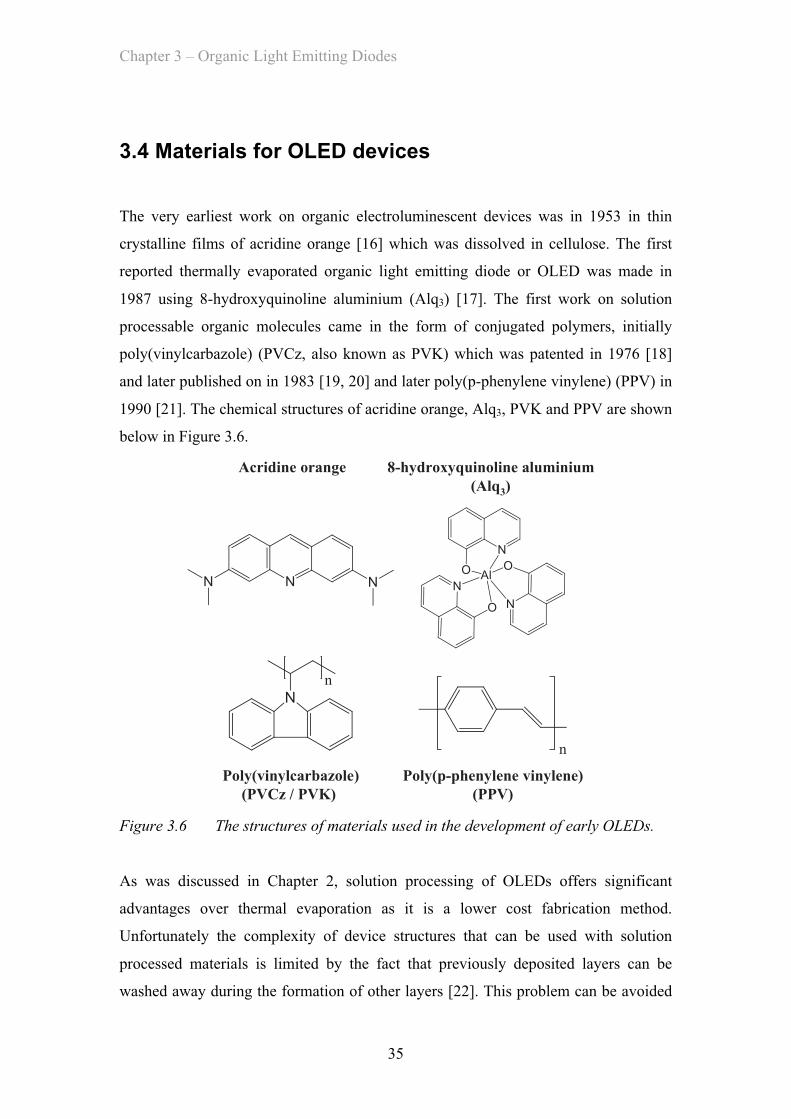
Chapter 3 – Organic Light Emitting Diodes
35
3.4 Materials for OLED devices
The very earliest work on organic electroluminescent devices was in 1953 in thin
crystalline films of acridine orange [16] which was dissolved in cellulose. The first
reported thermally evaporated organic light emitting diode or OLED was made in
1987 using 8-hydroxyquinoline aluminium (Alq3) [17]. The first work on solution
processable organic molecules came in the form of conjugated polymers, initially
poly(vinylcarbazole) (PVCz, also known as PVK) which was patented in 1976 [18]
and later published on in 1983 [19, 20] and later poly(p-phenylene vinylene) (PPV) in
1990 [21]. The chemical structures of acridine orange, Alq3, PVK and PPV are shown
below in Figure 3.6.
Poly(p-phenylene vinylene)(PPV)
Poly(vinylcarbazole)(PVCz / PVK)
8-hydroxyquinoline aluminium (Alq3)
Acridine orange
Figure 3.6 The structures of materials used in the development of early OLEDs.
As was discussed in Chapter 2, solution processing of OLEDs offers significant
advantages over thermal evaporation as it is a lower cost fabrication method.
Unfortunately the complexity of device structures that can be used with solution
processed materials is limited by the fact that previously deposited layers can be
washed away during the formation of other layers [22]. This problem can be avoided
Chapter 3 – Organic Light Emitting Diodes
36
by using orthogonal solvents for the next layer that will not dissolve the previous one.
A good example of this is the adding a layer of the water soluble conducting polymer
poly(3,4-ethylenedioxythiophene) poly(styrenesulfonate) or PEDOT:PSS [23]. This
polymer is often used to improve electrical contact and hole injection at the anode and
is insoluble in most organic solvents. Alternatively thermal [24, 25] or ultraviolet [26]
cross-linking can be used to make previous layers insoluble but these add processing
steps and put extra requirements on the materials used. As solution processing is
lower cost but multilayer evaporated small molecule devices can have higher
performance both approaches have been developed over the last two decades.
3.4.1 Host-Guest Blending
In a single material OLED the emissive material must also be optimised for its charge
transport properties and it can be difficult to optimise both emissive and charge
transport properties at the same time. An alternative is to use a second material to
transport the charge carriers and doping this material with the emissive material. This
strategy is called host-guest blending. The host can have a higher LUMO and lower
HOMO energy than the emissive material so that both charges hop off the host and
onto the emissive guest. This does not necessarily need to be the case however as
provided the energy gap of the guest is narrower than that of the host the excitations
will form on the host and lose energy transferring to the guest [27]. This can also
work with larger energy gaps provided the energy gap difference is lower than the
Boltzmann thermal energy [28]. If, however, the host has a lower energy gap than the
emissive material excitations can transfer back and be lost [29]. This can be
problematic for high energy blue emitters [30]. Preferably the host will also have a
long lifetime for excited states so that excitations will have a long time to transfer
from the host to the emissive guest.
3.4.2 Phosphorescent Emitters
In OLEDs most electrons and holes combine to form triplet excitons while only a
minority form singlet excitons in which can emit light in fluorescent materials. This
puts a significant limit on the efficiency of these materials. By incorporating heavy

Chapter 3 – Organic Light Emitting Diodes
37
metal complexes it is possible to make materials that can emit from the triplet state
and thus dramatically improve the maximum efficiency of devices. These materials
are said to be phosphorescent.
Only phosphorescent materials allow emission from both singlet and triplet excitons
[31, 32] that are formed within an electroluminescent device and thus allow 100%
internal quantum efficiency [4, 33-35]. Recently phosphorescent emitters have
allowed power efficiencies of 90 lm/W at 1,000 cd/m2 in white OLEDs that exceed
the 60-70 lm/W typical for fluorescent tubes [4].
Small molecules used to have the advantage over conjugated polymers in that they
could be heavy metal complexes, which allow phosphorescent emission where as
solution processable conjugated polymers were typically only capable of fluorescent
emission at room temperature. However, more recently phosphorescent polymers
have been develop like those discussed in Chapters 6 and 7.
An alternative approach is to make small molecules into solution processable
dendrimers by surrounding small molecule cores with branched dendrons which make
the cores soluble [36].
Singlet excitons form when a material is excited by an electric dipole transition when
absorbing a photon or under electrical excitation when an electron hole pair
recombines in such a way that their net spin is zero. In fluorescent materials these can
quickly relax to the ground state and emit light via a dipole transition without
difficulty. For the triplet exciton the electron hole pair forms in such a way as to have
a net spin of 1. These two types of excitons are illustrated in Figure 3.7.
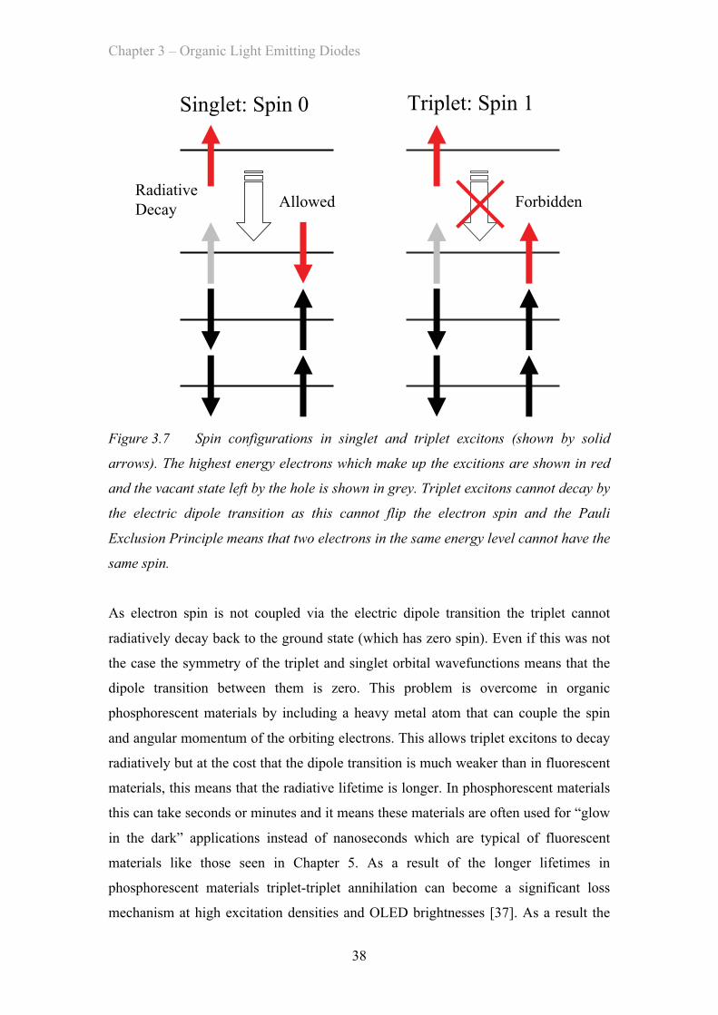
Chapter 3 – Organic Light Emitting Diodes
38
Singlet: Spin 0 Triplet: Spin 1
Allowed ForbiddenRadiativeDecay
Figure 3.7 Spin configurations in singlet and triplet excitons (shown by solid
arrows). The highest energy electrons which make up the excitions are shown in red
and the vacant state left by the hole is shown in grey. Triplet excitons cannot decay by
the electric dipole transition as this cannot flip the electron spin and the Pauli
Exclusion Principle means that two electrons in the same energy level cannot have the
same spin.
As electron spin is not coupled via the electric dipole transition the triplet cannot
radiatively decay back to the ground state (which has zero spin). Even if this was not
the case the symmetry of the triplet and singlet orbital wavefunctions means that the
dipole transition between them is zero. This problem is overcome in organic
phosphorescent materials by including a heavy metal atom that can couple the spin
and angular momentum of the orbiting electrons. This allows triplet excitons to decay
radiatively but at the cost that the dipole transition is much weaker than in fluorescent
materials, this means that the radiative lifetime is longer. In phosphorescent materials
this can take seconds or minutes and it means these materials are often used for “glow
in the dark” applications instead of nanoseconds which are typical of fluorescent
materials like those seen in Chapter 5. As a result of the longer lifetimes in
phosphorescent materials triplet-triplet annihilation can become a significant loss
mechanism at high excitation densities and OLED brightnesses [37]. As a result the
Chapter 3 – Organic Light Emitting Diodes
39
phosphorescent materials used in OLEDs have lifetimes order of 1 or 2 microseconds
in order to reduce triplet-triplet annihilation.
The ratio of singlets to triplets in electroluminescent devices might be expected to be
1 to 3 from the argument that there are 3 possible states making up the triplet (spin in
the z direction of 1, 0 or -1) and only one possible singlet state. This is referred to as
the spin – statistics argument. The exact ratio of singlets to triplets is difficult to
measure but this 1 to 3 ratio has been disputed [15, 38, 39]. For example careful
optical modelling could not explain the high efficiency of a poly(p-phenylene
vinylene) based OLEDs without invoking a higher ratio of singlets to triplets [15]. In
one case a phosphorescent polymer capable of giving emission from both singlets and
triplets, and doing so at different wavelengths, was used to probe the singlet to triplet
ratio [39]. In this case it was found that the individual monomers did indeed result in a
22 ± 1 % singlet states however in the case of the platinum based polymer the fraction
of triplet states was found to rise to 57 ± 4%. This result suggests that the ratio of
singlets to triplets can vary. This is believed to be based on different capture cross
sections for electron hole pairs dependent on their spin ratios. This effect seems to
cause divergence from the 1:3 ratio in some materials. Nevertheless phosphorescence
would still offer at least at least a factor 2 increase in the maximum quantum
efficiency of devices made with these materials.
Triplets have a lower energy than singlets in the same material because of the
exchange interaction. This results from the fact that electrons are fermions and thus
that they must have anti-symmetric wavefunctions under exchange (bosons are
symmetric under exchange). Anti-symmetric under exchange means that if any two
electrons are relabelled in the wavefunction for all the electrons in a system the sign
of the overall wavefunction must change. If the spin parts of the wavefunction are
symmetric under exchange (which is the case for a triplet) then the orbital parts of the
wavefunction are anti-symmetric which puts a greater distance between the electrons
minimising electrostatic repulsion. In the singlet, the spin parts of the wavefunction
are anti-symmetric and thus the orbital parts of the wavefunction must be symmetric
and so the electrostatic repulsion is higher. This can be seen most easily in a two
particle system. The two particle wavefunctions for the singlet and the three triplet
states are given below in Equation 3.10 and Equation 3.11-3.13 respectively. The
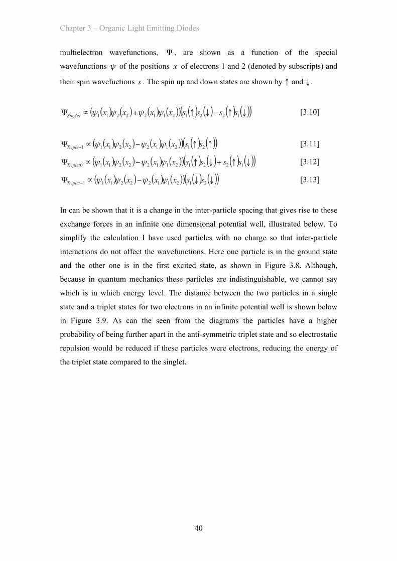
Chapter 3 – Organic Light Emitting Diodes
40
multielectron wavefunctions, Ψ , are shown as a function of the special
wavefunctions ψ of the positions x of electrons 1 and 2 (denoted by subscripts) and
their spin wavefuctions s . The spin up and down states are shown by ↑ and ↓.
( ) ( ) ( ) ( )( ) ( ) ( ) ( ) ( )( )↓↑−↓↑+∝Ψ 122121122211 ssssxxxxSinglet ψψψψ [3.10]
( ) ( ) ( ) ( )( ) ( ) ( )( )↑↑−∝Ψ + 21211222111 ssxxxxTriple ψψψψ [3.11]
( ) ( ) ( ) ( )( ) ( ) ( ) ( ) ( )( )↓↑+↓↑−∝Ψ 1221211222110 ssssxxxxTriplet ψψψψ [3.12]
( ) ( ) ( ) ( )( ) ( ) ( )( )↓↓−∝Ψ − 21211222111 ssxxxxTriplet ψψψψ [3.13]
In can be shown that it is a change in the inter-particle spacing that gives rise to these
exchange forces in an infinite one dimensional potential well, illustrated below. To
simplify the calculation I have used particles with no charge so that inter-particle
interactions do not affect the wavefunctions. Here one particle is in the ground state
and the other one is in the first excited state, as shown in Figure 3.8. Although,
because in quantum mechanics these particles are indistinguishable, we cannot say
which is in which energy level. The distance between the two particles in a single
state and a triplet states for two electrons in an infinite potential well is shown below
in Figure 3.9. As can the seen from the diagrams the particles have a higher
probability of being further apart in the anti-symmetric triplet state and so electrostatic
repulsion would be reduced if these particles were electrons, reducing the energy of
the triplet state compared to the singlet.
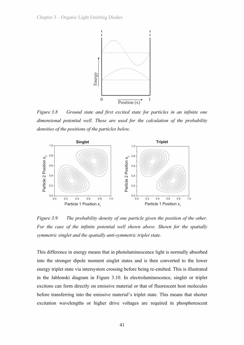
Chapter 3 – Organic Light Emitting Diodes
41
-1.1
-0.6
-0.1
0.4
0.9
0 0.3142 0.6284 0.9426 1.2568 1.571 1.8852 2.1994 2.5136 2.8278 3.142
-1.1
-0.6
-0.1
0.4
0.9
0 0.3142 0.6284 0.9426 1.2568 1.571 1.8852 2.1994 2.5136 2.8278 3.142
Ene
rgy
Position (x)0 1
Figure 3.8 Ground state and first excited state for particles in an infinite one
dimensional potential well. These are used for the calculation of the probability
densities of the positions of the particles below.
0.0 0.2 0.4 0.6 0.8 1.00.0
0.2
0.4
0.6
0.8
1.0
Singlet
Part
icle
2 P
ositio
n x
2
Particle 1 Position x1
0.0 0.2 0.4 0.6 0.8 1.00.0
0.2
0.4
0.6
0.8
1.0
Triplet
Part
icle
2 P
ositio
n x
2
Particle 1 Position x1
Figure 3.9 The probability density of one particle given the position of the other.
For the case of the infinite potential well shown above. Shown for the spatially
symmetric singlet and the spatially anti-symmetric triplet state.
This difference in energy means that in photoluminescence light is normally absorbed
into the stronger dipole moment singlet states and is then converted to the lower
energy triplet state via intersystem crossing before being re-emitted. This is illustrated
in the Jablonski diagram in Figure 3.10. In electroluminescence, singlet or triplet
excitons can form directly on emissive material or that of fluorescent host molecules
before transferring into the emissive material’s triplet state. This means that shorter
excitation wavelengths or higher drive voltages are required in phosphorescent
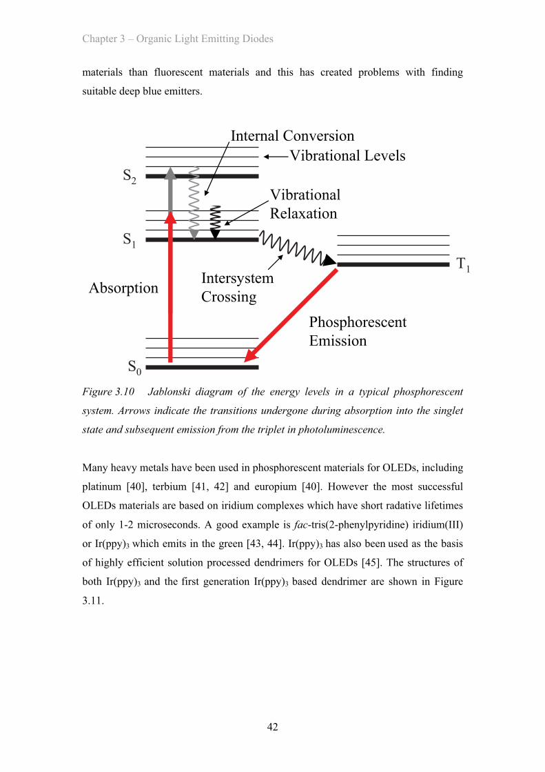
Chapter 3 – Organic Light Emitting Diodes
42
materials than fluorescent materials and this has created problems with finding
suitable deep blue emitters.
T1
S1
S2
S0
VibrationalRelaxation
IntersystemCrossing
PhosphorescentEmission
Absorption
Vibrational LevelsInternal Conversion
Figure 3.10 Jablonski diagram of the energy levels in a typical phosphorescent
system. Arrows indicate the transitions undergone during absorption into the singlet
state and subsequent emission from the triplet in photoluminescence.
Many heavy metals have been used in phosphorescent materials for OLEDs, including
platinum [40], terbium [41, 42] and europium [40]. However the most successful
OLEDs materials are based on iridium complexes which have short radative lifetimes
of only 1-2 microseconds. A good example is fac-tris(2-phenylpyridine) iridium(III)
or Ir(ppy)3 which emits in the green [43, 44]. Ir(ppy)3 has also been used as the basis
of highly efficient solution processed dendrimers for OLEDs [45]. The structures of
both Ir(ppy)3 and the first generation Ir(ppy)3 based dendrimer are shown in Figure
3.11.
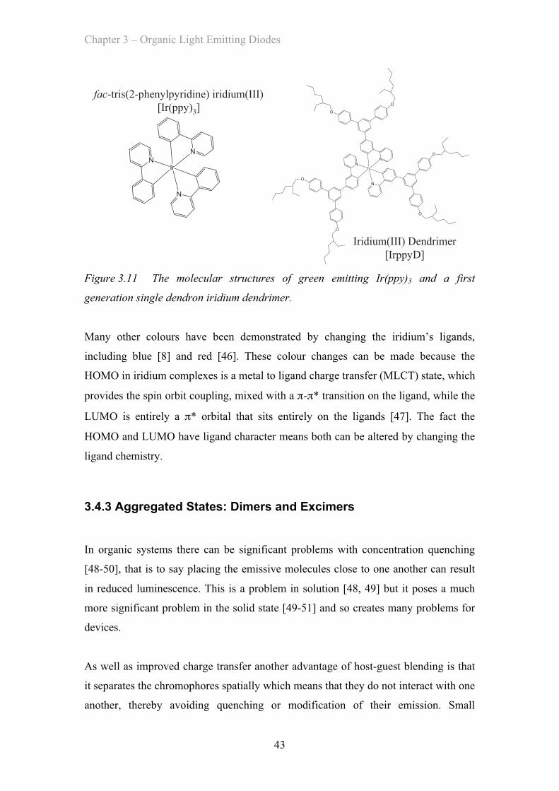
Chapter 3 – Organic Light Emitting Diodes
43
fac-tris(2-phenylpyridine) iridium(III)[Ir(ppy)3]
Iridium(III) Dendrimer[IrppyD]
Figure 3.11 The molecular structures of green emitting Ir(ppy)3 and a first
generation single dendron iridium dendrimer.
Many other colours have been demonstrated by changing the iridium’s ligands,
including blue [8] and red [46]. These colour changes can be made because the
HOMO in iridium complexes is a metal to ligand charge transfer (MLCT) state, which
provides the spin orbit coupling, mixed with a π-π* transition on the ligand, while the
LUMO is entirely a π* orbital that sits entirely on the ligands [47]. The fact the
HOMO and LUMO have ligand character means both can be altered by changing the
ligand chemistry.
3.4.3 Aggregated States: Dimers and Excimers
In organic systems there can be significant problems with concentration quenching
[48-50], that is to say placing the emissive molecules close to one another can result
in reduced luminescence. This is a problem in solution [48, 49] but it poses a much
more significant problem in the solid state [49-51] and so creates many problems for
devices.
As well as improved charge transfer another advantage of host-guest blending is that
it separates the chromophores spatially which means that they do not interact with one
another, thereby avoiding quenching or modification of their emission. Small
Chapter 3 – Organic Light Emitting Diodes
44
molecules are typically prone to π-stacking with one another and often quench each
other’s emission without a host. This means that if they were deposited from solution
they may phase separate and quench their luminescence, if used in high
concentrations. In polymers long, sterically bulky side groups are often added to
provide some protection against these concentration quenching effects [51, 52]. In
dendrimers the highly branched dendrons separate their cores, reducing inter-
chormophore interactions [36, 45, 53].
If two molecules are close enough to each other that their wavefunctions overlap then
they can form a system of coupled oscillators. This means the interaction potential
between the two molecules leads to splitting of molecular energy levels into higher
and lower states with oscillations on each molecule that are either in or out of phase.
If there is a superposition of these two stationary states the exciton can be thought of
as coherently moving back and forth between the two molecules. The dependence on
the splitting for the energy levels on the phase difference is illustrated in Figure 3.12.
Here the analogy of a pair of classical balls on springs interacting via a repulsive
electrostatic interaction is used. If the repulsion acts in the same direction as the
resulting force on the springs, the frequency of the oscillations is increased giving a
higher energy state. If the electrostatic repulsion acts against the springs the balls will
oscillate slower with lower energy. This means that for the head to tail configuration
the energy is lower when the balls are in phase and for the parallel configuration the
lower energy state has the balls oscillating out of phase. This is exactly what is found
in quantum mechanical dipole oscillations in molecules [54]. The head to tail
configuration where the lower energy state gives constructive inference is known as a
J aggregate while the parallel dipole case where the lower energy state is out of phase
is known as an H aggregate [55, 56].
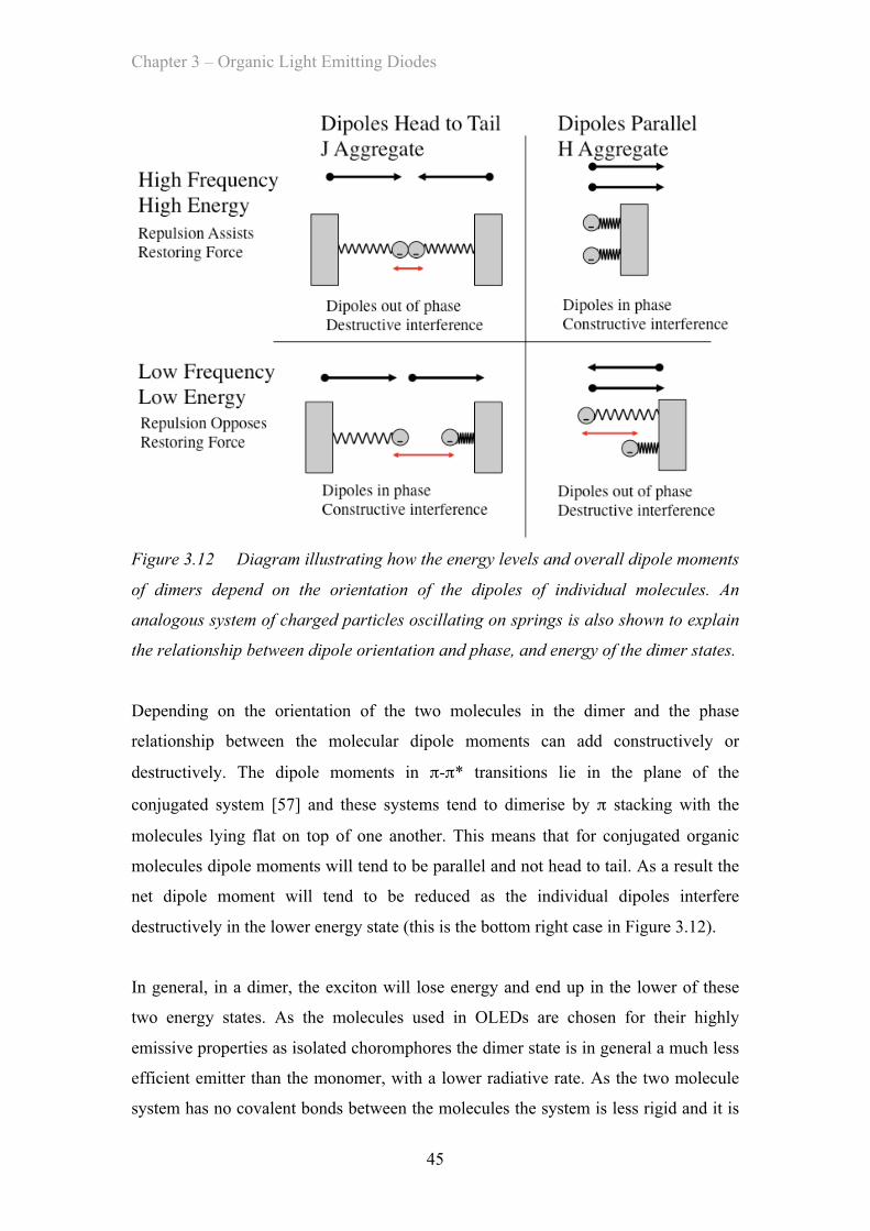
Chapter 3 – Organic Light Emitting Diodes
45
Figure 3.12 Diagram illustrating how the energy levels and overall dipole moments
of dimers depend on the orientation of the dipoles of individual molecules. An
analogous system of charged particles oscillating on springs is also shown to explain
the relationship between dipole orientation and phase, and energy of the dimer states.
Depending on the orientation of the two molecules in the dimer and the phase
relationship between the molecular dipole moments can add constructively or
destructively. The dipole moments in π-π* transitions lie in the plane of the
conjugated system [57] and these systems tend to dimerise by π stacking with the
molecules lying flat on top of one another. This means that for conjugated organic
molecules dipole moments will tend to be parallel and not head to tail. As a result the
net dipole moment will tend to be reduced as the individual dipoles interfere
destructively in the lower energy state (this is the bottom right case in Figure 3.12).
In general, in a dimer, the exciton will lose energy and end up in the lower of these
two energy states. As the molecules used in OLEDs are chosen for their highly
emissive properties as isolated choromphores the dimer state is in general a much less
efficient emitter than the monomer, with a lower radiative rate. As the two molecule
system has no covalent bonds between the molecules the system is less rigid and it is
Chapter 3 – Organic Light Emitting Diodes
46
likely to have a higher non-radiative de-excitation rate. As the properties of a dimer
system depend on the position and orientation of the molecules involved this means
that in a system containing dimers there is a collection of many different emissive
species. This means aggregated systems tend to have broad, featureless, red-shifted
and less efficient emission than the systems of isolated molecules. However in some
unusual cases emission from organic molecules can be enhanced by dimerisation [49].
Like dimers, excimers are formed when two molecules or atoms come together to
form an aggregate. However unlike dimers, excimers are atoms or molecules which
only come together when one is in the excited state. Excimer lasers use gas atoms
which bond together after one has been excited to form a single emissive species by
collision with another atom. They are commonly used to produce high power ultra-
violet light for applications such as lithography for making semiconductor chips.
Excimer emission has also been used to make highly efficient broad spectrum
phosphorescent organic light emitting diodes [58-60]. This broad featureless spectrum
has made them good candidate for white OLED devices using only a single emissive
material [58]. Like normal dimers, excimers typically lead to a red-shifting of the
emission spectrum compared to the monomer and (despite the above examples) are
often less emissive than the isolated monomers and so usually undesirable.
3.4 Design of OLEDs
3.4.1 Charge Injection
Before electroluminescence can happen charges must be injected into the device.
With inorganic materials this means electrons must be injected into the conduction
band and holes into the valance band. In organic materials this means electrons must
move to occupy the lowest unoccupied molecular orbital (LUMO) and holes are
injected by removing a charge from the highest occupied molecular orbital (HOMO).
This is shown in Figure 3.13. In both cases if there is an energy gap between the work
function of the contact and the energy level being injected into then there can be a
barrier to charge injection [61]. The work function is the energy required to remove an
electron from the material and allow it to escape into vacuum, such as via the
photoelectric effect.
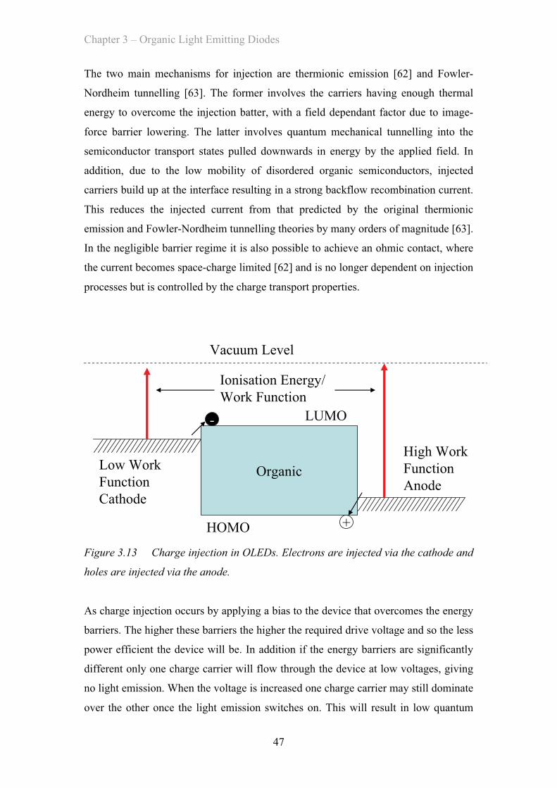
Chapter 3 – Organic Light Emitting Diodes
47
The two main mechanisms for injection are thermionic emission [62] and Fowler-
Nordheim tunnelling [63]. The former involves the carriers having enough thermal
energy to overcome the injection batter, with a field dependant factor due to image-
force barrier lowering. The latter involves quantum mechanical tunnelling into the
semiconductor transport states pulled downwards in energy by the applied field. In
addition, due to the low mobility of disordered organic semiconductors, injected
carriers build up at the interface resulting in a strong backflow recombination current.
This reduces the injected current from that predicted by the original thermionic
emission and Fowler-Nordheim tunnelling theories by many orders of magnitude [63].
In the negligible barrier regime it is also possible to achieve an ohmic contact, where
the current becomes space-charge limited [62] and is no longer dependent on injection
processes but is controlled by the charge transport properties.
Organic
HOMO
LUMO
Low Work FunctionCathode
High Work FunctionAnode
Vacuum Level
Ionisation Energy/ Work Function
-
+
Figure 3.13 Charge injection in OLEDs. Electrons are injected via the cathode and
holes are injected via the anode.
As charge injection occurs by applying a bias to the device that overcomes the energy
barriers. The higher these barriers the higher the required drive voltage and so the less
power efficient the device will be. In addition if the energy barriers are significantly
different only one charge carrier will flow through the device at low voltages, giving
no light emission. When the voltage is increased one charge carrier may still dominate
over the other once the light emission switches on. This will result in low quantum
Chapter 3 – Organic Light Emitting Diodes
48
efficiency as a current is flowing but not all the charges will recombine, reducing
captureη in Equation 3.4. In OLEDs it is often harder to inject electrons than holes and
this means that low workfunction, and thus reactive metals, such as calcium,
magnesium or barium are often needed as the cathode material
3.4.2 Electrode Quenching
Once the charges have been injected they must move through the device to recombine
and form excitons which can emit light. This charge transport typically has a field and
temperature dependent mobility due to the disordered energy levels in amorphous
organic materials (as discussed in Chapter 2). Significantly for OLEDs the electron
mobility in organic materials is often orders of magnitude lower than the hole
mobility [64]. This means that in situations where the charge injection is perfectly
balanced the charge carriers often recombine very close to the cathode.
As the cathode is very often a metal, or is at the very least conductive, it produces
image charges and dipoles in response to the charges and excitons in the organic
layer. If a molecule is trying to emit too close to the contact (say one tenth of a
wavelength in the medium) then the dipole and the image dipole will interfere out of
phase with one another and luminescence will be significantly reduced [15]. In
addition the metal dielectric interface can support surface plasmon modes which can
be excited by nearby emissive molecules [65]. These modes are trapped within the
device and so do not contribute to light emission.
3.4.3 Charge Transport Layers
In order to improve charge injection, achieve charge balance and keep recombining
charges away from the electrodes hole-transport and electron-transport layers can be
used [66]. These materials can perform these roles by having suitable HOMO and
LUMO levels as shown in Figure 3.14. Charge injection at the electrodes can be
improved by having a lower energy barrier at the electrodes. This necessitates another
small energy step inside the device when the charge carriers reach the emissive layer
but these small energy barriers are easier to overcome by mechanisms such as
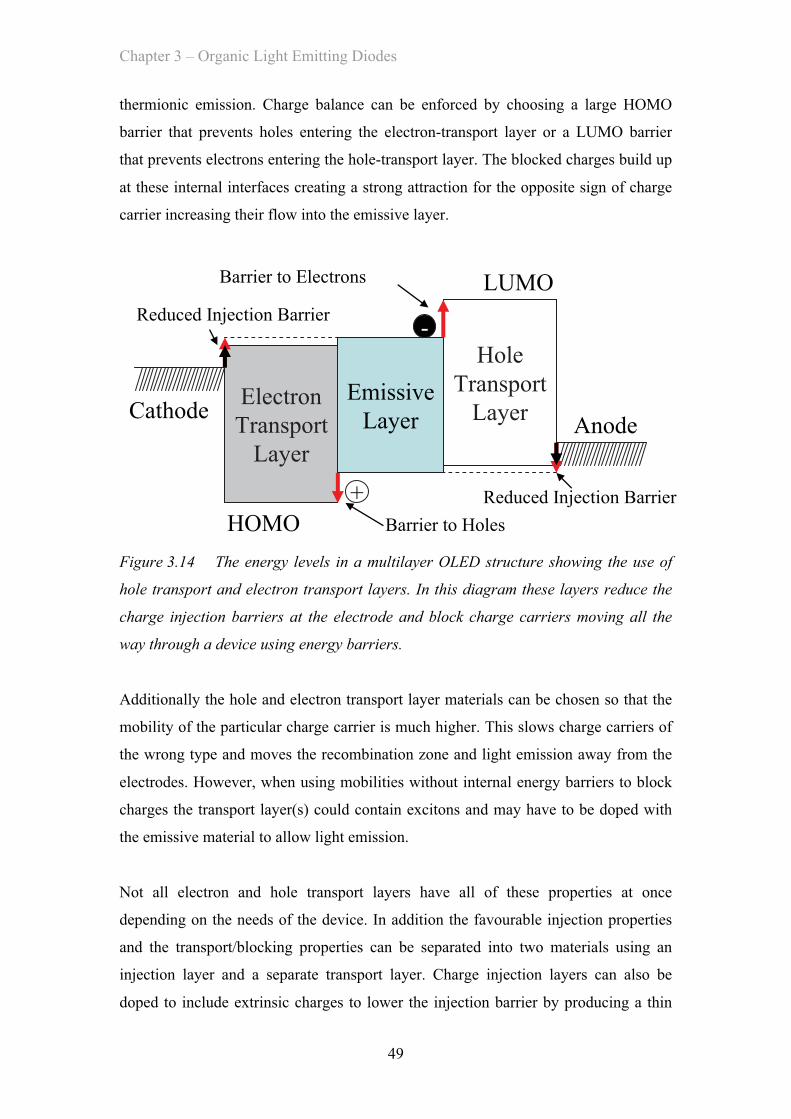
Chapter 3 – Organic Light Emitting Diodes
49
thermionic emission. Charge balance can be enforced by choosing a large HOMO
barrier that prevents holes entering the electron-transport layer or a LUMO barrier
that prevents electrons entering the hole-transport layer. The blocked charges build up
at these internal interfaces creating a strong attraction for the opposite sign of charge
carrier increasing their flow into the emissive layer.
ElectronTransport
Layer
HoleTransport
LayerEmissive
Layer
HOMO
LUMO
CathodeAnode
-
+Barrier to Holes
Barrier to Electrons
Reduced Injection Barrier
Reduced Injection Barrier
Figure 3.14 The energy levels in a multilayer OLED structure showing the use of
hole transport and electron transport layers. In this diagram these layers reduce the
charge injection barriers at the electrode and block charge carriers moving all the
way through a device using energy barriers.
Additionally the hole and electron transport layer materials can be chosen so that the
mobility of the particular charge carrier is much higher. This slows charge carriers of
the wrong type and moves the recombination zone and light emission away from the
electrodes. However, when using mobilities without internal energy barriers to block
charges the transport layer(s) could contain excitons and may have to be doped with
the emissive material to allow light emission.
Not all electron and hole transport layers have all of these properties at once
depending on the needs of the device. In addition the favourable injection properties
and the transport/blocking properties can be separated into two materials using an
injection layer and a separate transport layer. Charge injection layers can also be
doped to include extrinsic charges to lower the injection barrier by producing a thin
Chapter 3 – Organic Light Emitting Diodes
50
depletion region, which helps align the electrodes workfunction with the organic
semiconductor’s HOMO or LUMO [67, 68]. This can lead to devices with 5 or more
layers. This can be achieved using thermal evaporation but it is increasingly difficult
to add multiple layers to solution processed devices. Therefore in solution processed
devices it is better if materials properties allow efficient devices with only one or two
layers [22].
3.4.4 Light Extraction
As only ~20% of light leaves conventional OLED structures, improved light
extraction efficiency offers a way to make large gains in performance. Unfortunately
the cost is often increased device complexity if the light extraction enhancement is
within the device or blurring of pixels with their neighbours if the enhancement is
applied to the substrate.
Strategies that have been tried for enhancing emission from the layer itself include
incorporating photonic crystals [69-72], inserting a low refractive index grid to scatter
light [73], patterning the organic layer into a Bragg grating by imprinting [74],
buckling the reflective electrode [75] or using a semi-transparent electrode to create a
micro-cavity [76]. These approaches can give ~100% improvement in quantum
efficiency [75]. Unfortunately the strategies that use periodic gratings or microcavities
also lead to angle dependent emission and colour, which is not ideal unless another
layer is added to scatter the light and restore even lambertian emission [9].
Adding a diffuser [9], microlens array [73] or luminaire [77] to the top of the device is
generally an easier way to enhance emission but is only suitable for large area single
colour lighting or signage applications. Again the outcoupling efficiency can be
approximately doubled using these approaches [77]. Since it offers such large
improvements in device performance, it is using out-coupling enhancement in
addition to the optimisation of all the other device and material parameters discussed
above that has allowed the most efficient white OLEDs with over 100 lm/W power
efficiency [4].
Chapter 3 – Organic Light Emitting Diodes
51
1. Friend, R.H., et al., Electroluminescence in conjugated polymers. Nature, 1999. 397(6715): p. 121-128.
2. Py, C., et al., High-contrast organic light emitting diodes with a partially absorbing anode. Optics Letters, 2008. 33(10): p. 1126-1128.
3. Braun, D., et al., Nanosecond Transient Electronluminescence From Polymer Light Emitting Diodes. Applied Physics Letters, 1992. 61(26): p. 3092-3094.
4. Reineke, S., et al., White organic light-emitting diodes with fluorescent tube efficiency. Nature, 2009. 459(7244): p. 234-U116.
5. D'Andrade, B.W. and S.R. Forrest, White organic light-emitting devices for solid-state lighting. Advanced Materials, 2004. 16(18): p. 1585-1595.
6. Misra, A., et al., White organic LEDs and their recent advancements. Semiconductor Science and Technology, 2006. 21(7): p. R35-R47.
7. Commission Internationale de l’Éclairage Proceedings, 1931.1931: Cambridge University Press.
8. Tokito, S., et al., Confinement of triplet energy on phosphorescent molecules for highly-efficient organic blue-light-emitting devices. Applied Physics Letters, 2003. 83(3): p. 569-571.
9. Mulder, C.L., et al., Saturated and efficient blue phosphorescent organic light emitting devices with Lambertian angular emission. Applied Physics Letters, 2007. 90(21).
10. Demas, J.N. and G.A. Crosby, Measurement of Photoluminescence Quantum Yields - Review. Journal of Physical Chemistry, 1971. 75(8): p. 991.
11. Greenham, N.C., et al., Measurement of Absolute Photoluminescence Quantum Efficiencies in Conjugated Polymers. Chemical Physics Letters, 1995. 241(1-2): p. 89-96.
12. Liu, Z.T., et al., The characterization of the optical functions of BCP and CBP thin films by spectroscopic ellipsometry. Synthetic Metals, 2005. 150(2): p. 159-163.
13. Greenham, N.C., R.H. Friend, and D.D.C. Bradley, Angular-Dependance of the Emission From a Conjugated Polymer Light-Emitting Diode - Implications For Efficiency Calculations. Advanced Materials, 1994. 6(6): p. 491-494.
14. Khalfin, V.B., et al., Weak microcavity effects in organic light-emitting devices. 1998. - 58(- 7).
15. Kim, J.-S., et al., Electroluminescence emission pattern of organic light-emitting diodes: Implications for device efficiency calculations. Journal of Applied Physics, 2000. 88(2): p. 1073.
16. Bernanose, A., M. Comte, and P. Vouaux, Sur un nouveau mode d'émission lumineuse chez certains composés organiques. J. Chim. Phys. , 1953. 50: p. 64.
17. Tang, C.W. and S.A. VanSlyke, Organic electroluminescent diodes. Applied Physics Letters, 1987. 51(12): p. 913-915.
18. Partridge, R.H., Radiation Sources. U.S. Patent: 3995299, 1975. 19. Partridge, R.H., Electro-Luminescence From Polyvinylcarbazyole Films .3.
Electroluminescent Devices. Polymer, 1983. 24(6): p. 748-754. 20. Partridge, R.H., Electro-Luminescence From Polyvinylcarbazyole Films .4.
Electro-Luminescence Usuing Higher Work Function Cathodes. Polymer, 1983. 24(6): p. 755-762.
21. Burroughes, J.H., et al., Light-emitting diodes based on conjugated polymers. Nature, 1990. 347: p. 539 - 541.
Chapter 3 – Organic Light Emitting Diodes
52
22. Forrest, S.R., The path to ubiquitous and low-cost organic electronic appliances on plastic. Nature, 2004. 428: p. 911.
23. Brown, T.M., et al., Built-in field electroabsorption spectroscopy of polymer light-emitting diodes incorporating a doped poly(3,4-ethylene dioxythiophene) hole injection layer. Applied Physics Letters, 1999. 75(12): p. 1679-1681.
24. Yan, H., et al., High-performance hole-transport layers for polymer light-emitting diodes. Implementation of organosiloxane cross-linking chemistry in polymeric electroluminescent devices. Journal of the American Chemical Society, 2005. 127(9): p. 3172-3183.
25. Klarner, G., et al., Cross-linkable polymers based on dialkylfluorenes. Chemistry of Materials, 1999. 11(7): p. 1800-1805.
26. Contoret, A.E.A., et al., The photopolymerization and cross-linking of electroluminescent liquid crystals containing methacrylate and diene photopolymerizable end groups for multilayer organic light-emitting diodes. Chemistry of Materials, 2002. 14(4): p. 1477-1487.
27. Jeon, W.S., et al., Ideal host and guest system in phosphorescent OLEDs. Organic Electronics, 2009. 10(2): p. 240-246.
28. Holmes, R.J., et al., Blue organic electrophosphorescence using exothermic host-guest energy transfer. Applied Physics Letters, 2003. 82(15): p. 2422-2424.
29. Sudhakar, M., et al., Phosphorescence quenching by conjugated polymers. Journal of the American Chemical Society, 2003. 125(26): p. 7796-7797.
30. Yeh, S.J., et al., New dopant and host materials for blue-light-emitting phosphorescent organic electroluminescent devices. Advanced Materials, 2005. 17(3): p. 285-+.
31. Malliaras, G. and R. Friend, An organic electronics primer. Physics Today, 2005. 58(5): p. 53-58.
32. Baldo, M.A., et al., Highly efficient phosphorescent emission from organic electroluminescent devices. Nature, 1998. 395(6698): p. 151-154.
33. Adachi, C., et al., Nearly 100% internal phosphorescence efficiency in an organic light-emitting device. Journal of Applied Physics, 2001. 90(10): p. 5048-5051.
34. Wang, Q., et al., Harvesting Excitons Via Two Parallel Channels for Efficient White Organic LEDs with Nearly 100% Internal Quantum Efficiency: Fabrication and Emission-Mechanism Analysis. Advanced Functional Materials, 2009. 19(1): p. 84-95.
35. Williams, E.L., et al., Excimer-based white phosphorescent organic light emitting diodes with nearly 100 % internal quantum efficiency. Advanced Materials, 2007. 19(2): p. 197.
36. Burn, P.L., S.C. Lo, and I.D.W. Samuel, The development of light-emitting dendrimers for displays. Advanced Materials, 2007. 19(13): p. 1675-1688.
37. Baldo, M.A., C. Adachi, and S.R. Forrest, Transient analysis of organic electrophosphorescence. II. Transient analysis of triplet-triplet annihilation. Physical Review B, 2000. 62(16): p. 10967-10977.
38. Cao, Y., et al., Improved quantum efficiency for electroluminescence in semiconducting polymers. Nature, 1999. 397(6718): p. 414-417.
39. Wilson, J.S., et al., Spin-dependent exciton formation in pi-conjugated compounds. Nature, 2001. 413(6858): p. 828-831.
40. !!! INVALID CITATION !!!
Chapter 3 – Organic Light Emitting Diodes
53
41. Capecchi, S., et al., High-efficiency organic electroluminescent devices using an organoterbium emitter. Advanced Materials, 2000. 12(21): p. 1591-+.
42. Kido, J. and Y. Okamoto, Organo lanthanide metal complexes for electroluminescent materials. Chemical Reviews, 2002. 102(6): p. 2357-2368.
43. King, K.A., P.J. Spellane, and R.J. Watts, Excited-State Properties of a Triply Ortho-Metalated Iridium(III) Complex. Journal of the American Chemical Society, 1985. 107(5): p. 1431-1432.
44. Baldo, M.A., et al., Very high-efficiency green organic light-emitting devices based on electrophosphorescence. Applied Physics Letters, 1999. 75(1): p. 4-6.
45. Lo, S.C., et al., Green phosphorescent dendrimer for light-emitting diodes. Advanced Materials, 2002. 14(13-14): p. 975.
46. Tsuboyama, A., et al., Homoleptic cyclometalated iridium complexes with highly efficient red phosphorescence and application to organic light-emitting diode. Journal of the American Chemical Society, 2003. 125(42): p. 12971-12979.
47. Hay, P.J., Theoretical studies of the ground and excited electronic states in cyclometalated phenylpyridine Ir(III) complexes using density functional theory. Journal of Physical Chemistry A, 2002. 106(8): p. 1634-1641.
48. Melhuish, W.H., Quantum Efficiencies of Fluorescence of Organic Substances: Effect of Solvent and Concentration on the Fluorescent Solute. Journal of Physical Chemistry, 1961. 65: p. 229.
49. Hong, Y.N., J.W.Y. Lam, and B.Z. Tang, Aggregation-induced emission: phenomenon, mechanism and applications. Chemical Communications, 2009(29): p. 4332-4353.
50. Schouwink, P., et al., The influence of molecular aggregation on the device properties of organic light emitting diodes. Thin Solid Films, 2000. 372(1-2): p. 163-168.
51. Setayesh, S., et al., Polyfluorenes with polyphenylene dendron side chains: Toward non-aggregating, light-emitting polymers. Journal of the American Chemical Society, 2001. 123(5): p. 946-953.
52. Gambino, S., A.K. Bansal, and I.D.W. Samuel, Comparison of hole mobility in thick and thin films of a conjugated polymer. Organic Electronics, 2010. 11(3): p. 467-471.
53. Lo, S.C., et al., Encapsulated cores: Host-free organic light-emitting diodes based on solution-processible electrophosphorescent dendrimers. Advanced Materials, 2005. 17(16): p. 1945-+.
54. Pope, M. and C.S. Swenberg, Electronic Processes in Organic Crystals and Polymers (2nd Edition). 2 ed1982: Oxford University Press.
55. Gadde, S., et al., Control of H- and J-Aggregate Formation via Host-Guest Complexation using Cucurbituril Hosts. Journal of the American Chemical Society, 2008. 130(50): p. 17114-17119.
56. Ghosh, S., et al., Control of H- and J-Type pi Stacking by Peripheral Alkyl Chains and Self-Sorting Phenomena in Perylene Bisimide Homo- and Heteroaggregates. Chemistry-a European Journal, 2008. 14(36): p. 11343-11357.
57. Birge, R.R., et al., Transition dipole orientation of linear polyenes: Semiempirical models and extrapolation to the infinite chain limit. Journal of Physical Chemistry A, 1999. 103(14): p. 2251-2255.
Chapter 3 – Organic Light Emitting Diodes
54
58. Kalinowski, J., et al., Mixing of excimer and exciplex emission: A new way to improve white light emitting organic electrophosphorescent diodes. Advanced Materials, 2007. 19(22): p. 4000-+.
59. Cocchi, M., et al., Highly efficient near-infrared organic excimer electrophosphorescent diodes. Applied Physics Letters, 2007. 90(2).
60. Kalinowski, J., et al., Bi-molecular emissive excited states in platinum (II) complexes for high-performance organic light-emitting diodes. Chemical Physics, 2010. 378(1-3): p. 47-57.
61. Brown, T.M., et al., Electronic line-up in light-emitting diodes with alkali-halide/metal cathodes. Journal of Applied Physics, 2003. 93(10): p. 6159-6172.
62. Davids, P.S., I.H. Campbell, and D.L. Smith, Device model for single carrier organic diodes. Journal of Applied Physics, 1997. 82(12): p. 6319-6325.
63. Davids, P.S., et al., Charge injection in organic light-emitting diodes: Tunneling into low mobility materials. Applied Physics Letters, 1996. 69(15): p. 2270-2272.
64. So, F., et al., Recent progress in solution processable organic light emitting devices. Journal of Applied Physics, 2007. 102(9).
65. Hobson, P.A., et al., The role of surface plasmons in organic light-emitting diodes. Ieee Journal of Selected Topics in Quantum Electronics, 2002. 8(2): p. 378-386.
66. Kulkarni, A.P., et al., Electron transport materials for organic light-emitting diodes. Chemistry of Materials, 2004. 16(23): p. 4556-4573.
67. Pfeiffer, M., et al., Doped organic semiconductors: Physics and application in light emitting diodes. Organic Electronics, 2003. 4(2-3): p. 89-103.
68. Walzer, K., et al., Highly efficient organic devices based on electrically doped transport layers. Chemical Reviews, 2007. 107(4): p. 1233-1271.
69. Ziebarth, J.M. and M.D. McGehee, A theoretical and experimental investigation of light extraction from polymer light-emitting diodes. Journal of Applied Physics, 2005. 97(6).
70. Do, Y.R., et al., Enhanced light extraction efficiency from organic light emitting diodes by insertion of a two-dimensional photonic crystal structure. Journal of Applied Physics, 2004. 96(12): p. 7629-7636.
71. Matterson, B.J., et al., Increased efficiency and controlled light output from a microstructured light-emitting diode. Advanced Materials, 2001. 13(2): p. 123-127.
72. Lupton, J.M., et al., Bragg scattering from periodically microstructured light emitting diodes. Applied Physics Letters, 2000. 77(21): p. 3340-3342.
73. Sun, Y. and S.R. Forrest, Enhanced light out-coupling of organic light-emitting devices using embedded low-index grids. Nature Photonics, 2008. 2(8): p. 483-487.
74. Yates, C.J., et al., Surface plasmon-polariton mediated emission from phosphorescent dendrimer light-emitting diodes. Applied Physics Letters, 2006. 88(16).
75. Koo, W.H., et al., Light extraction from organic light-emitting diodes enhanced by spontaneously formed buckles. Nature Photonics, 2010. 4(4): p. 222-226.
76. Meerheim, R., R. Nitsche, and K. Leo, High-efficiency monochrome organic light emitting diodes employing enhanced microcavities. Applied Physics Letters, 2008. 93(4).
Chapter 3 – Organic Light Emitting Diodes
55
77. D'Andrade, B.W. and J.J. Brown, Organic light-emitting device luminaire for illumination applications. Applied Physics Letters, 2006. 88(19).
56
4. Experimental Methods
4.1 Overview ................................................................................................................ 56�4.2 Phosphorescence Quenching by Oxygen ............................................................... 57�4.3 Absorption and Photoluminescence Spectra .......................................................... 58�4.4 Photoluminescence Quantum Yield (PLQY) ......................................................... 58�
4.4.1 Solution PLQY ............................................................................................ 58�4.4.2 Film PLQY .................................................................................................. 60�4.4.3 Powder PLQY ............................................................................................. 62�4.4.4 CCD and Integrating Sphere Method ......................................................... 63�
4.5 Time-Correlated Single Photon Counting ............................................................. 64�4.6 OLED Device Fabrication ..................................................................................... 65�4.7 OLED Characterisation .......................................................................................... 69�
4.7.1 External Quantum Efficiency Calculation .................................................. 70�4.7.2 Luminous Efficiency Calculation ............................................................... 72�
4.1 Overview
This chapter contains an overview of many of the experimental methods used
throughout this work. The importance of and methods for keeping samples oxygen
free is discussed in Section 4.2. Absorption and photoluminescence spectroscopy is
essential to most of the methods and is described in Section 4.3. Section 4.4 is
concerned with the measurement of the photoluminescence quantum yield (PLQY) of
materials. Section 4.5 covers the Time-Correlated Single Photon Counting (TCSPC)
method for determining the luminescence lifetime of materials. Section 4.6 contains a
description of the methods for making OLED devices and Section 4.7 cover OLED
characterisation.
The PLQY of a material is the efficiency with which incident photons are re-emitted
as luminescence, and as was explained in chapter 3 this is an important parameter for
luminescent devices in its own right. However the PLQY also offers greater insight
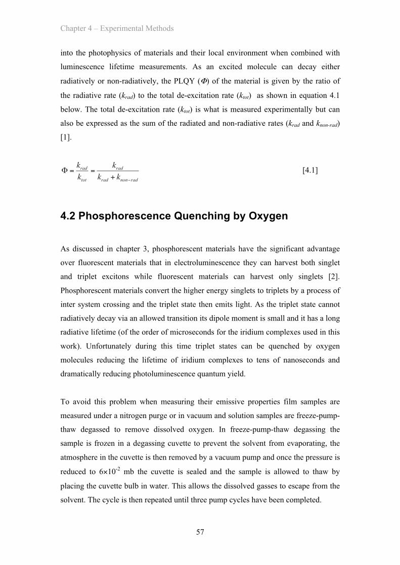
Chapter 4 – Experimental Methods
57
into the photophysics of materials and their local environment when combined with
luminescence lifetime measurements. As an excited molecule can decay either
radiatively or non-radiatively, the PLQY (Φ) of the material is given by the ratio of
the radiative rate (krad) to the total de-excitation rate (ktot) as shown in equation 4.1
below. The total de-excitation rate (ktot) is what is measured experimentally but can
also be expressed as the sum of the radiated and non-radiative rates (krad and knon-rad)
[1].
radnonrad
rad
tot
rad
kkk
kk
−+==Φ [4.1]
4.2 Phosphorescence Quenching by Oxygen
As discussed in chapter 3, phosphorescent materials have the significant advantage
over fluorescent materials that in electroluminescence they can harvest both singlet
and triplet excitons while fluorescent materials can harvest only singlets [2].
Phosphorescent materials convert the higher energy singlets to triplets by a process of
inter system crossing and the triplet state then emits light. As the triplet state cannot
radiatively decay via an allowed transition its dipole moment is small and it has a long
radiative lifetime (of the order of microseconds for the iridium complexes used in this
work). Unfortunately during this time triplet states can be quenched by oxygen
molecules reducing the lifetime of iridium complexes to tens of nanoseconds and
dramatically reducing photoluminescence quantum yield.
To avoid this problem when measuring their emissive properties film samples are
measured under a nitrogen purge or in vacuum and solution samples are freeze-pump-
thaw degassed to remove dissolved oxygen. In freeze-pump-thaw degassing the
sample is frozen in a degassing cuvette to prevent the solvent from evaporating, the
atmosphere in the cuvette is then removed by a vacuum pump and once the pressure is
reduced to 6×10⁻² mb the cuvette is sealed and the sample is allowed to thaw by
placing the cuvette bulb in water. This allows the dissolved gasses to escape from the
solvent. The cycle is then repeated until three pump cycles have been completed.

Chapter 4 – Experimental Methods
58
4.3 Absorption and Photoluminescence Spectra
Absorption measurements in either film or solution were made using a Varian Cary
300 spectrophotometer. This instrument uses a differential measurement between the
monochromated light transmitted through a reference and the sample. In the case of a
film measurement the reference used is a clean substrate, and for solution
measurments it is a cuvette containing the same solvent. The reference allows the
instrument to account for any loses due to reflections, scattering or absorption by the
substrate, cuvette or solvent. The bandpass of the monochromator was set to 2 nm.
The absorbance or optical density (α(λ)) of the sample at a given wavelength (λ) is
calculated using formula 4.2 below where (T(λ)) is the transmitted light through the
sample and (T0(λ)) is the transmitted light through the reference.
( ) ( )( )⎟
⎟⎠
⎞⎜⎜⎝
⎛−=
λλ
λα0
10logTT
[4.2]
Photoluminescence measurements were made using a Jobin Yvon Fluoromax 2
fluorimeter. The instrument used monochromated light to excite the sample and then
another monochromator was used to collect the emitted light. The excitation and
emission bandpass were 1 nm. The spectral response of the instrument was corrected
by multiplying the spectra by a known calibration curve and all spectra were
measured in terms of number of photons detected per unit wavelength.
4.4 Photoluminescence Quantum Yield (PLQY)
4.4.1 Solution PLQY
Solution PLQY measurements were made using the method from Demas and Crosby
[3] which involves comparing the luminescence of the sample to a reference in a fixed
measurement geometry and with the same excitation wavelength. Here we use the
Jobin Yvon Flouromax 2 flourimeter. Unless noted otherwise a solution of quinine
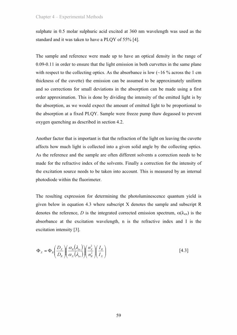
Chapter 4 – Experimental Methods
59
sulphate in 0.5 molar sulphuric acid excited at 360 nm wavelength was used as the
standard and it was taken to have a PLQY of 55% [4].
The sample and reference were made up to have an optical density in the range of
0.09-0.11 in order to ensure that the light emission in both curvettes in the same plane
with respect to the collecting optics. As the absorbance is low (~16 % across the 1 cm
thickness of the cuvette) the emission can be assumed to be approximately uniform
and so corrections for small deviations in the absorption can be made using a first
order approximation. This is done by dividing the intensity of the emitted light is by
the absorption, as we would expect the amount of emitted light to be proportional to
the absorption at a fixed PLQY. Sample were freeze pump thaw degassed to prevent
oxygen quenching as described in section 4.2.
Another factor that is important is that the refraction of the light on leaving the cuvette
affects how much light is collected into a given solid angle by the collecting optics.
As the reference and the sample are often different solvents a correction needs to be
made for the refractive index of the solvents. Finally a correction for the intensity of
the excitation source needs to be taken into account. This is measured by an internal
photodiode within the fluorimeter.
The resulting expression for determining the photoluminescence quantum yield is
given below in equation 4.3 where subscript X denotes the sample and subscript R
denotes the reference, D is the integrated corrected emission spectrum, α(λex) is the
absorbance at the excitation wavelength, n is the refractive index and I is the
excitation intensity [3].
( )( ) ⎟⎟
⎠
⎞⎜⎜⎝
⎛⎟⎟⎠
⎞⎜⎜⎝
⎛⎟⎟⎠
⎞⎜⎜⎝
⎛⎟⎟⎠
⎞⎜⎜⎝
⎛Φ=Φ
X
R
R
X
exX
exR
R
XRX I
Inn
DD
2
2
λαλα
[4.3]
Chapter 4 – Experimental Methods
60
4.4.2 Film PLQY
For most of this work film PLQY measurements were made using the Greenham
method [1] which uses a laser as an excitation source and makes use of an integrating
sphere to collect the light emitted in all directions. The reason for this is that film
samples often show angle-dependent emission because the films have thicknesses
comparable to the wavelength of the emitted light and so a measurement at just one
angle, such as in the solution PLQY method discussed above, would give misleading
results. The fact polymers tend to lie in the place of the substrate, but small molecules
or dendrimers might not, also means all emission angles need to be integrated over.
The intensity of the re-emitted light compared to the excitation intensity is determined
by an NPL calibrated photodiode supplied by Bentham attached to a Labsphere
integrating sphere. The 325 nm line of a Kimmon Electric 1K He:Cd laser was used
as the excitation source. The photodiode signal from the laser beam in the sphere with
no sample present (Xlaser) is measured to determine amount of excitation light. To
determine the quantity of luminescence produced by the sample a long pass filter is
placed in front of the photodiode and the sample is placed in the beam and the
photodiode signal is recorded (Xsample) while the sphere was purged with nitrogen to
prevent oxygen quenching. A diagram showing these measurements is given in Figure
4.1.
As not all the excitation light is absorbed by the film corrections have to be made for
secondary fluorescence generated by laser light which is reflected on the first strike
and absorbed later by the sample. Firstly a measurement of the fraction of laser light
reflected (R) and transmitted (T) by the sample has to be made outside the integrating
sphere. Then the amount of signal produced by the secondary luminescence must be
quantified. This is done by placing the sample in the sphere but out of the path of the
laser beam and measuring the photodiode signal through the long pass filter (Xsphere).
This is shown in Figure 4.1. The secondary fluorescence because of the reflected and
transmitted light is then subtracted from signal on the photodiode when the sample is
in the beam.
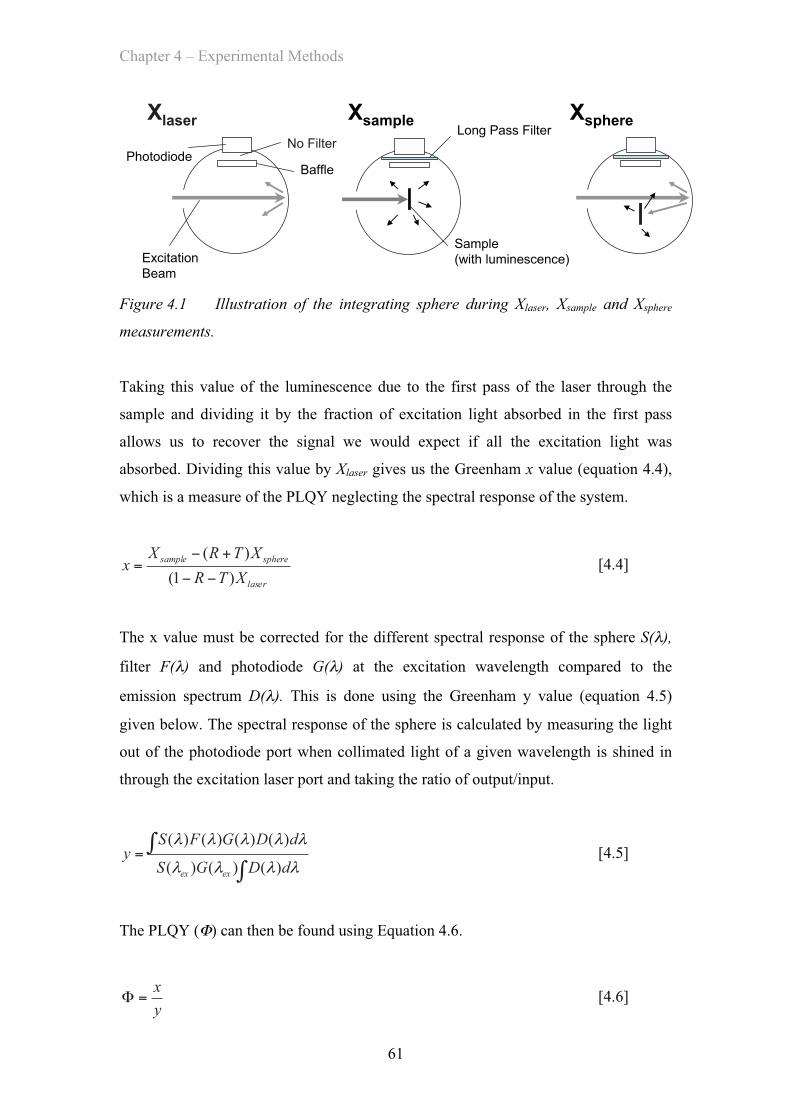
Chapter 4 – Experimental Methods
61
XlaserNo Filter
PhotodiodeBaffle
Long Pass Filter
Sample
(with luminescence)Excitation
Beam
Xsample Xsphere
Figure 4.1 Illustration of the integrating sphere during Xlaser, Xsample and Xsphere
measurements.
Taking this value of the luminescence due to the first pass of the laser through the
sample and dividing it by the fraction of excitation light absorbed in the first pass
allows us to recover the signal we would expect if all the excitation light was
absorbed. Dividing this value by Xlaser gives us the Greenham x value (equation 4.4),
which is a measure of the PLQY neglecting the spectral response of the system.
laser
spheresample
XTRXTRX
x)1(
)(
−−
+−= [4.4]
The x value must be corrected for the different spectral response of the sphere S(λ),
filter F(λ) and photodiode G(λ) at the excitation wavelength compared to the
emission spectrum D(λ). This is done using the Greenham y value (equation 4.5)
given below. The spectral response of the sphere is calculated by measuring the light
out of the photodiode port when collimated light of a given wavelength is shined in
through the excitation laser port and taking the ratio of output/input.
∫∫=
λλλλ
λλλλλ
dDGS
dDGFSy
exex )()()(
)()()()( [4.5]
The PLQY (Φ) can then be found using Equation 4.6.
yx
=Φ [4.6]
Chapter 4 – Experimental Methods
62
4.4.3 Powder PLQY
PLQY measurements from powders were performed using a method similar to the
Greenham [1] method, however an Andor Model DV420-BV CCD spectrometer was
used to determine the amount of scattered light from the sample as a simple
measurement of transmitted and reflected does not account for all the scattered light
[5].
A method for using just a CCD spectrometer to measure PLQY has been developed
by de Mello [6] however it relies on the spectrometer being calibrated over a wide
range of wavelengths from the excitation to the longest emission wavelengths and
also requires a large dynamic range. Due to difficulties in finding a suitable
calibration light source over this wide wavelength range a method based on adapting
the Greenham and de Mello approaches so that an uncalibrated CCD spectrometer
could be used to measure the scattered light [5].
The CCD spectrometer was attached to the integrating sphere for the measurements
along with the photodiode described in Section 4.5. The intensity of the scattered light
was determined by integrating the laser line in the spectrum of the CCD when the
sample is in the beam (Csample).
In order to determine the fraction of scattered laser light it is also necessary to
determine the intensity of the light exciting the sample. However a spectrometer
measurement of the laser intensity with no sample in the sphere (Claser) would not be
sufficient as the spectral response of the sphere is significantly altered by the presence
of a sample that absorbs at the excitation wavelengths.
The change in the spectral response can be determined from the ratio of the
spectrometer signal with the sample in the sphere but out of the beam (Csphere) to the
Claser measurement. This causes the Claser measurement to cancel out. Thus the
fraction of scattered light is given by equation 4.7.
Chapter 4 – Experimental Methods
63
sphere
sample
CC
S = [4.7]
This scattered light can then be used to correct for the secondary fluorescence using
equation 4.4 using S in the place of R+T and the PLQY can be determined using
equation 4.6.
4.4.4 CCD and Integrating Sphere Method
Some PLQY measurements were made using a commercial Hamamatsu C9920-02
measurement system using the method published by Suzuki [7]. Here the excitation is
provided by a monochromated Xenon lamp coupled into an integrating sphere via an
optical fibre. The method works by using a CCD spectrometer attached to the sphere
via another fibre optic cable to measure the spectrum of the light in the integrating
sphere. Two spectra are taken: one with a blank reference and then another with the
sample in place. In each case the excitation and emission parts of the spectrum (in
photons per wavelength) are integrated, after a spectral correction for the detectors,
optics and sphere response has been applied. This yields ( )referenceE λ and ( )sampleE λ (the
excitation spectra with the reference and then the sample in place) and ( )referenceD λ and
( )sampleD λ (the emission spectra). The PLQY can then be calculated using Equation
[4.8].
( ) ( )( ) ( )∫
∫−
−=Φ
λλλ
λλλ
dEE
dDD
samplereference
referencesample [4.8]
This simple equation can be used because the integrating sphere used has >99%
reflectivity over the entire spectral range so a change path length of the average
photons before reaching the detector due to the presence of an absorbing sample is not
large. Therefore the calculations involving scattered light, discussed above in Section
4.4.3, are not needed. This method can be used for films, solution and powder and is
relatively fast as it requires only two measurements using the CCD spectrometer.
Chapter 4 – Experimental Methods
64
However it requires a high quality integrating sphere that is kept very clean to
maintain its high reflectivity across all wavelengths.
4.5 Time-Correlated Single Photon Counting Time-correlated single photon counting is a technique that determines the time delay
between an excitation pulse and the detection of an emitted photon from a sample to
build up statistics about its time dependent emission. The time between the excitation
pulse and the arrival of the first photon at the detector is determined using a time to
amplitude converter (TAC) which converts it to an electrical signal that can be
recorded by a computer. The detected signal intensity is kept low enough so that the
count rate of photons is less than 5% of the excitation repetition frequency so that the
probability of multiple photons arriving at the detector as the result of a single pulse is
low. This is important because the TAC cannot detect multiple photons from a single
pulse and thus multiple photons would lead to skewed statistics.
In these experiments a Picoquant LDH C400 393 nm GaN laser diode and a twice
frequency doubled Alphalas Pulselas-532-30-P Nd:YAG microchip laser at 266 nm
were used as excitation sources. The GaN laser diode resulted in an instrument
response function of <300 ps full width half maximum and the Nd:YAG laser gave a
response of ~500 ps full width half maximum. The detector used was a Hamamatsu
RU-3809 U-50 micro-channel plate photomultiplier tube behind a monochromator to
select the emission wavelength and a filter for the excitation light. Solution samples
were freeze pump thaw degassed as described in Section 4.2 and film samples were
measured in vacuum to prevent oxygen quenching or sample degradation.
For short lifetime fluorescent the data was analysed using an iterative reconvolution
method to take account of the response function. The goodness of fit was calculated
using a chi-squared parameter using Poissonian errors and this value was minimised
over multiple iterations.
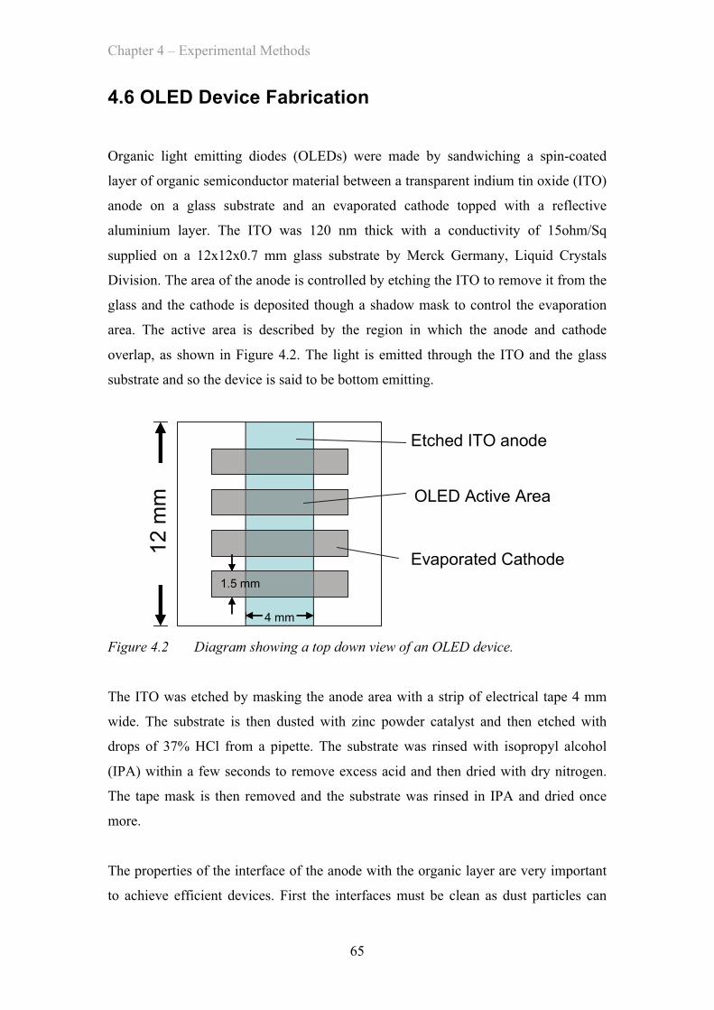
Chapter 4 – Experimental Methods
65
4.6 OLED Device Fabrication
Organic light emitting diodes (OLEDs) were made by sandwiching a spin-coated
layer of organic semiconductor material between a transparent indium tin oxide (ITO)
anode on a glass substrate and an evaporated cathode topped with a reflective
aluminium layer. The ITO was 120 nm thick with a conductivity of 15ohm/Sq
supplied on a 12x12x0.7 mm glass substrate by Merck Germany, Liquid Crystals
Division. The area of the anode is controlled by etching the ITO to remove it from the
glass and the cathode is deposited though a shadow mask to control the evaporation
area. The active area is described by the region in which the anode and cathode
overlap, as shown in Figure 4.2. The light is emitted through the ITO and the glass
substrate and so the device is said to be bottom emitting.
Etched ITO anode
Evaporated Cathode
OLED Active Area
12 m
m
4 mm
1.5 mm
Figure 4.2 Diagram showing a top down view of an OLED device.
The ITO was etched by masking the anode area with a strip of electrical tape 4 mm
wide. The substrate is then dusted with zinc powder catalyst and then etched with
drops of 37% HCl from a pipette. The substrate was rinsed with isopropyl alcohol
(IPA) within a few seconds to remove excess acid and then dried with dry nitrogen.
The tape mask is then removed and the substrate was rinsed in IPA and dried once
more.
The properties of the interface of the anode with the organic layer are very important
to achieve efficient devices. First the interfaces must be clean as dust particles can
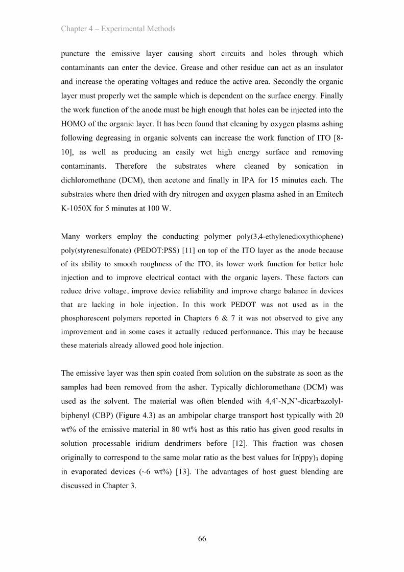
Chapter 4 – Experimental Methods
66
puncture the emissive layer causing short circuits and holes through which
contaminants can enter the device. Grease and other residue can act as an insulator
and increase the operating voltages and reduce the active area. Secondly the organic
layer must properly wet the sample which is dependent on the surface energy. Finally
the work function of the anode must be high enough that holes can be injected into the
HOMO of the organic layer. It has been found that cleaning by oxygen plasma ashing
following degreasing in organic solvents can increase the work function of ITO [8-
10], as well as producing an easily wet high energy surface and removing
contaminants. Therefore the substrates where cleaned by sonication in
dichloromethane (DCM), then acetone and finally in IPA for 15 minutes each. The
substrates where then dried with dry nitrogen and oxygen plasma ashed in an Emitech
K-1050X for 5 minutes at 100 W.
Many workers employ the conducting polymer poly(3,4-ethylenedioxythiophene)
poly(styrenesulfonate) (PEDOT:PSS) [11] on top of the ITO layer as the anode because
of its ability to smooth roughness of the ITO, its lower work function for better hole
injection and to improve electrical contact with the organic layers. These factors can
reduce drive voltage, improve device reliability and improve charge balance in devices
that are lacking in hole injection. In this work PEDOT was not used as in the
phosphorescent polymers reported in Chapters 6 & 7 it was not observed to give any
improvement and in some cases it actually reduced performance. This may be because
these materials already allowed good hole injection.
The emissive layer was then spin coated from solution on the substrate as soon as the
samples had been removed from the asher. Typically dichloromethane (DCM) was
used as the solvent. The material was often blended with 4,4’-N,N’-dicarbazolyl-
biphenyl (CBP) (Figure 4.3) as an ambipolar charge transport host typically with 20
wt% of the emissive material in 80 wt% host as this ratio has given good results in
solution processable iridium dendrimers before [12]. This fraction was chosen
originally to correspond to the same molar ratio as the best values for Ir(ppy)3 doping
in evaporated devices (~6 wt%) [13]. The advantages of host guest blending are
discussed in Chapter 3.

Chapter 4 – Experimental Methods
67
N
N N
N
NN
NN
TPBI
CBP
Figure 4.3 The chemical structures of charge transport host 4,4’-N,N’-
dicarbazolyl-biphenyl (CBP) and electron transport/hole blocking material 1,3,5,-
tris(2-N-phenylbenzimidazolyl)benzene (TPBI).
After spin-coating the samples were placed on a shadow mask for the deposition of
1.5 mm stripes of the subsequent layers shown in Figure 4.2 and placed in an Edwards
FL 400 evaporator operating at a pressure of 10-6 mb. The area of shadow mask and
ITO overlap defines the active area of the OLED devices. This transfer was made as
quickly as possible to avoid sample contamination or degradation.
The evaporated layers deposited were different for single layer and bi-layer devices. A
diagram showing both structures can be found in Figure 4.4. Single layer devices used
a 20 nm low work function calcium layer for electron injection and were then topped
with >100 nm of aluminium to protect the calcium from oxygen and to increase the
cathode conductivity. Bi-layer devices used a second evaporated organic layer of 60
nm of 1,3,5,-tris(2-N-phenylbenzimidazolyl)benzene (TPBI) as an electron transport /
hole blocking layer (structure in Figure 4.3). This ensures that the electron and hole
currents in the device are well balanced as discussed in chapter 3.
Chapter 4 – Experimental Methods
68
Al
Ca
Emissive Layer
ITO
Glass
Al
Emissive Layer
ITO
Glass
TPBILiF 0.7 nm
Single Layer OLED Bi-Layer OLED
20 nm
>100 nm
125 nm
60 nm
Figure 4.4 Single layer and bi-layer OLED structures.
The cathode is then evaporated on top of the TPBI layer. This consisted of a thin 0.7
nm layer of LiF and topped with >100 nm of aluminium. LiF has been shown to
improve electron injection into some organic materials when used with aluminium
[14] or calcium [15] cathodes. An advantage of Al/LiF cathodes over low work
function metals is that it has increased chemical stability as an electrode.
Unfortunately LiF’s effectiveness seems to depend on the organic material deposited
beneath it and so it cannot be used in all cases. Here we use it because of its known
effectiveness on TPBI with an aluminium capping layer.
LiF must be deposited as a thin layer as bulk LiF is an insulator and so it can only be
effective by modifying the properties at the interface. Proposed mechanisms have
been the formation of a LiF dipole monolayer that reduces the work function of the
aluminium, liberation of lithium metal to function as a low work function contact or
doping of the organic layer with Li+ ions [15]. Similar effects could be the reason that
thin layers of MgO, CsF and Li3PO4 are also found to be effective [14-16].
More generally it is thought possible that any hot evaporated material can react
chemically with the organic layer, the metal deposited above it or both to induce inter-
band defect states into the organic which permit easier charge injection. These inter-
band states are believed to exist and make electron injection easier even when less
reactive materials like ITO are evaporated onto organic layers [17]. In this case ITO
was used as the substrate and was also evaporated onto the top of the organic layer
meaning that both cathode and anode should have similar work functions and thus
Chapter 4 – Experimental Methods
69
charge injection properties. However it was found that only the evaporated ITO
contact could inject electrons and function as the cathode. This shows that the
evaporation of the ITO caused an improvement in electron injection.
4.7 OLED Characterisation
The OLEDs were characterised in vacuum to avoid oxygen quenching or sample
degradation during the measurement. The current / voltage characteristics were
recorded using a Keithley 2400 Sourcemeter and the emission intensity was measured
using a calibrated photodiode with a surface area of 1 cm2 at a distance of 4 cm from
the sample. The photodiode current was put through a transimpedance amplifier and
the resulting voltage measured by a Keithley 2000 Multimeter. The emission
spectrum of the OLED was measured using an Andor DV420-BV CCD spectrometer.
This emission spectrum was also used to correct for the spectral response of the
photodiode in order to determine the external quantum efficiency and match it to the
eye’s brightness response to allow measurement in photometric units.
In order to calculate the fraction of emitted light collected by the photodiode the
emission of the OLED is assumed to be Lambertian meaning that the intensity of the
emitted light goes as the cosine of the viewing angle from the normal. To simplify the
calculation the square photodiode is taken to be a circle with the same active area (1
cm2). The OLED is 4 cm from the detector and this is assumed to be sufficiently
distant from the detector compared to the OLED’s size (1.5 mm × 4 mm) that it can
be taken as a point source and it is assumed to be aligned with the centre of the
detector. The photodiode is taken to be the base of a cone of angle α with the point at
the OLED as shown in Figure 4.5.

Chapter 4 – Experimental Methods
70
OLED
d=4 cm
1 cm
Photodiode
α r
Figure 4.5 The geometry of the OLED and photodiode in the OLED
characterisation setup.
The fraction of light emitted into the cone described by the angle α compared to the
forward hemisphere by a Lambertian emitter (emission )cos(θ∝ ) is given by
Equation 4.9.
( )22
22
2/
0
0det sin
)sin()cos(2
)sin()cos(2
drr
d
d
+==
•
•=
∫∫ α
θθθπ
θθθπη π
α
[4.9]
4.7.1 External Quantum Efficiency Calculation
The external quantum efficiency of an OLED is a measure of the number of photons
emitted by the device for each electron worth of charge that crosses the device. As
discussed in chapter 3, this parameter gives insight into how close to the theoretical
maximum efficiency can be achieved by a given material but is not in itself an
important parameter in a useful device.
As this quantity depends on the number of photons emitted if the spectral responsivity
of the photodetector R(λ) expressed in current per unit incident power then this
number needs to be converted into a quantum efficiency E(λ) in order to determine
the number of photons N collected from the detected current I. For a single
wavelength λ this is done by multiplying R(λ) by the photon energy and dividing by
Chapter 4 – Experimental Methods
71
the charge on an electron e. This is shown in Equation 4.10 where h is plank’s
constant and c is the speed of light in vacuum.
( ) ( )λ
λλehcRE = [4.10]
The average quantum efficiency of the detector for the emission spectrum of the
sample B(λ) should thus be calculated by Equation 4.11.
( ) ( ) ( )
( )∫∫
==λλ
λλλ
λ
λλ
dBe
dRBhcRehcEavg [4.11]
The voltage measured by the Keithley 2000 Multimeter (Vdet) as a result of the
photocurrent (Idet) depends on the value of the transimpedance amplifier (Zdet) as
shown in Equation 4.12.
detdetdet ZIV = [4.12]
Taking both the fraction of light collected by the photodiode (Equation 4.9) and the
photodiode’s quantum efficiency (Equation 4.11) it is possible to calculate the number
of emitted photons. By dividing this by the OLED current IOLED the external quantum
efficiency (ηex) can be calculated using Equation 4.13.
( )
( ) ( ) ⎥⎦
⎤⎢⎣
⎡⎥⎦
⎤⎢⎣
⎡
⎥⎥⎥
⎦
⎤
⎢⎢⎢
⎣
⎡
⎥⎦
⎤⎢⎣
⎡ +=
∫∫
OLEDex IZ
V
dRBhc
dBer
dr 1
det
det2
22
λλλ
λ
λλη [4.13]

Chapter 4 – Experimental Methods
72
4.7.2 Luminous Efficiency Calculation
The brightness of a device as observed by the human eye is a useful parameter for
both display and lighting applications. The human eye’s relative brightness response
to a given incident power given by )(λy is not the same over all wavelengths and
peaks in the green as shown in Figure 4.6 [18]. This means that blue and red light
sources of a given power appear dimmer than the equivalent green light. In order to
account for this the emission spectrum of the OLED needs to be taken into account to
determine the perceived brightness.
400 500 600 7000.0
0.2
0.4
0.6
0.8
1.0
Bri
gh
tne
ss R
esp
on
se
of
Hu
ma
n E
ye
/ In
cid
en
t P
ow
er
Wavelength /nm
Figure 4.6 The brightness response of the human eye to incident power at a given
wavelength )(λy .
The perceived brightness of light sources is measured in photometric units (as
opposed to radiometric units for measurements of power). Photometric units are
lumens (lm) which measure the total light output of a device and is most suitable for
lighting applications. How bright a point light source appears at a distance is
measured in candela (cd), which is a lumen per steradian. Brightness of displays or
other extended light sources that are viewed directly is measured in candela per metre
squared.
Chapter 4 – Experimental Methods
73
In order to determine the brightness of an OLED it is necessary to correct for the
difference in the responsivity R(λ) of the photodiode to that of the human eye )(λy to
the emitted power spectrum of the OLED. The relative value is scaled by the peak
response Km of 683 lm/W to given an absolute response in lumens per watt. The
power spectrum can be calculated by simply taking the emission spectrum, B(λ) in
photons per unit wavelength, and dividing by the emission wavelength λ. This can be
compared to the equivalent integral for the photodiode to give the measured
photocurrent per lumen incident on the detector (the photopic response RPhotopic). This
is given by Equation 4.14.
∫
∫∞
∞
=
0
0
./)()(
./)()(
λλλβλ
λλλβλ
dyK
dRR
m
Photopic [4.14]
Using the fraction of light emitted collected by the detector from Equation 4.9 and the
gain of the transimpedance amplifier the number of lumens of light emitted by the
OLED, F, can be calculated using Equation [4.15].
refPhotopic ZV
RrdrF det
2
22 1⎥⎦
⎤⎢⎣
⎡ += [4.14]
The assuming Lambertion emission the number of lumens per steradian or candelas in
the forward direction, L, is calculated by determining emission in the forward
direction divided by the total emission into the forward hemisphere as given in
Equation [4.16].
( ) ( ) πφθθθ
ππ
1
sincos
)0cos(2
0
2/
0
==
∫ ∫ ddf [4.16]
Chapter 4 – Experimental Methods
74
Thus the brightness of the device in candelas, L, can be determined using Equation
[4.17].
refPhotopic ZV
RrdrL det
2
22 11⎥⎦
⎤⎢⎣
⎡ +=π
[4.17]
1. Greenham, N.C., et al., Measurement of Absolute Photoluminescence
Quantum Efficiencies in Conjugated Polymers. Chemical Physics Letters, 1995. 241(1-2): p. 89-96.
2. Baldo, M.A., et al., Highly efficient phosphorescent emission from organic electroluminescent devices. Nature, 1998. 395(6698): p. 151-154.
3. Demas, J.N. and G.A. Crosby, Measurement of Photoluminescence Quantum Yields - Review. Journal of Physical Chemistry, 1971. 75(8): p. 991.
4. Melhuish, W.H., Quantum Efficiencies of Fluorescence of Organic Substances: Effect of Solvent and Concentration on the Fluorescent Solute. Journal of Physical Chemistry, 1961. 65: p. 229.
5. Levell, J.W., et al., Fluorescence Enhancement by Symmetry Breaking in a Twisted Triphenylene Derivative. Journal of Physical Chemistry A, 2010. 114(51): p. 13291.
6. de Mello, J.C., H.F. Wittmann, and R.H. Friend, An improved experimental determination of external photoluminescence quantum efficiency. Advanced Materials, 1997. 9(3): p. 230-&.
7. Suzuki, K., et al., Reevaluation of absolute luminescence quantum yields of standard solutions using a spectrometer with an integrating sphere and a back-thinned CCD detector. Physical Chemistry Chemical Physics, 2009. 11(42): p. 9850-9860.
8. Kim, J.S., et al., Indium-tin oxide treatments for single- and double-layer polymeric light-emitting diodes: The relation between the anode physical, chemical, and morphological properties and the device performance. Journal of Applied Physics, 1998. 84(12): p. 6859-6870.
9. Wu, C.C., et al., Surface modification of indium tin oxide by plasma treatment: An effective method to improve the efficiency, brightness, and reliability of organic light emitting devices. Applied Physics Letters, 1997. 70(11): p. 1348-1350.
10. Fujita, S., et al., Surface treatment of indium-tin-oxide substrates and its effects on initial nucleation processes of diamine films. Japanese Journal of Applied Physics Part 1-Regular Papers Short Notes & Review Papers, 1997. 36(1A): p. 350-353.
11. Brown, T.M., et al., Built-in field electroabsorption spectroscopy of polymer light-emitting diodes incorporating a doped poly(3,4-ethylene dioxythiophene) hole injection layer. Applied Physics Letters, 1999. 75(12): p. 1679-1681.
12. Lo, S.C., et al., Green phosphorescent dendrimer for light-emitting diodes. Advanced Materials, 2002. 14(13-14): p. 975.
13. Baldo, M.A., et al., Very high-efficiency green organic light-emitting devices based on electrophosphorescence. Applied Physics Letters, 1999. 75(1): p. 4-6.
Chapter 4 – Experimental Methods
75
14. Hung, L.S., C.W. Tang, and M.G. Mason, Enhanced electron injection in organic electroluminescence devices using an Al/LiF electrode. Applied Physics Letters, 1997. 70(2): p. 152-154.
15. Brown, T.M., et al., Electronic line-up in light-emitting diodes with alkali-halide/metal cathodes. Journal of Applied Physics, 2003. 93(10): p. 6159-6172.
16. Gassmann, A., et al., Interface properties of a Li3PO4 /Al cathode in organic light emitting diodes. Journal of Applied Physics, 2009. 105: p. 124517.
17. Parthasarathy, G., et al., High-efficiency transparent organic light-emitting devices. Applied Physics Letters, 2000. 76(15): p. 2128-2130.
18. Commission Internationale de l’Éclairage Proceedings, 1931.1931: Cambridge University Press.
76
5. Fluorescent Enhancement Using a Twisted Tripheneylene Derivative
5.1 Introduction ............................................................................................................ 76�5.2 Measuring Oscillator Strength ............................................................................... 78�5.3 Results and Discussion .......................................................................................... 81�
5.3.1 Absorption Properties ................................................................................. 81�5.3.2 Emission Properties .................................................................................... 84�
5.4 OLED Measurements ............................................................................................. 92�5.5 Conclusion ............................................................................................................. 92�
5.1 Introduction Aggregation effects, described in Chapter 3, often result in quenching of
luminescence in organic light emitting materials. This problem is also referred to as
concentration quenching as the light emission is quenched by two or more of the
emissive chromophores interfering with one another [1, 2]. These interactions appear
in solution but result in greater problems in the solid state as the molecules are much
closer together so excitations can diffuse to lower energy quenching sites [3, 4].
Various strategies are used to control aggregation in light emitting materials. Bulky
side groups can be attached to conjugated polymers [4, 5], branching dendrimer arms
can be attached to emissive cores [6-8] or higher energy host molecules can be used to
physically separate the cores. Another approach is to twist the geometry of the
molecules out of a single plane so that stacking is not possible, for example in the case
of spiro-fluorenes [9]. In this chapter I explore an exampole of this last type of
aggregation.
Triphenylene is an example of a planar molecule which is prone to aggregation by π
stacking. In fact it is commonly used to make columnar structures for liquid crystals
[10-13]. In this work, I have investigated the improvement in the fluorescence
efficiency of triphenylene when additional methyl groups are added to the 1,4,5,8,9
and 12 positions which forces the molecule out of the plane [14]. This modified
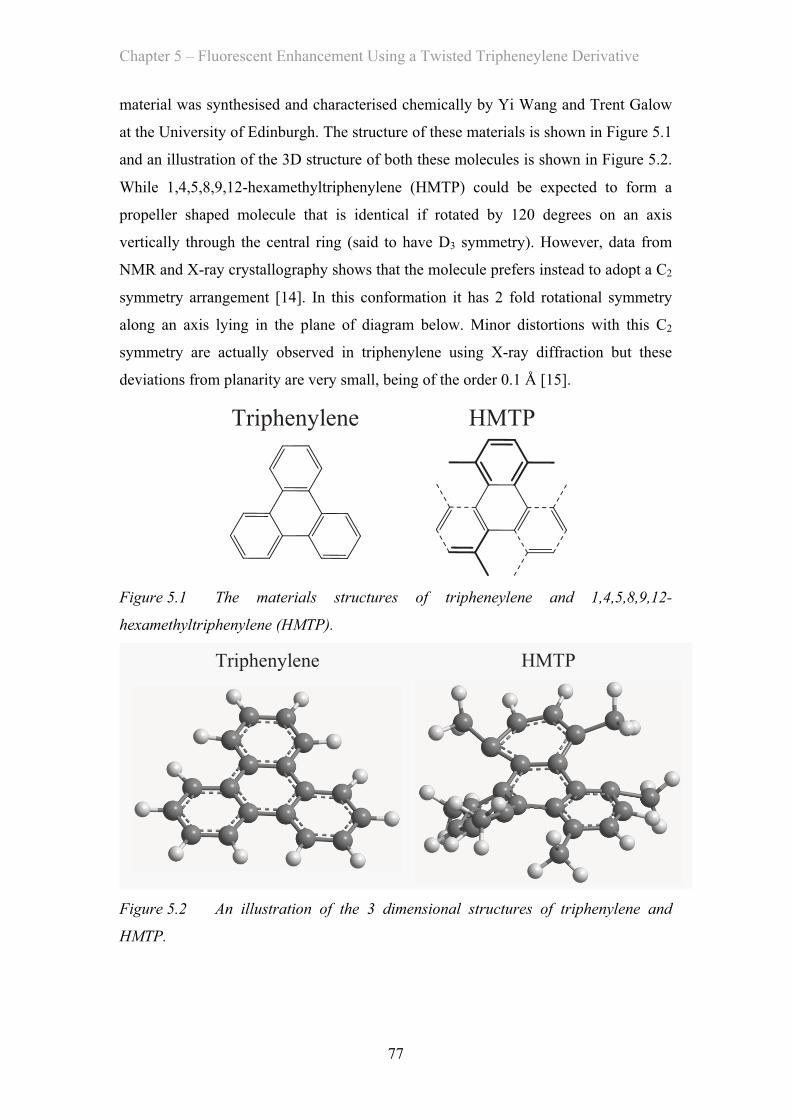
Chapter 5 – Fluorescent Enhancement Using a Twisted Tripheneylene Derivative
77
material was synthesised and characterised chemically by Yi Wang and Trent Galow
at the University of Edinburgh. The structure of these materials is shown in Figure 5.1
and an illustration of the 3D structure of both these molecules is shown in Figure 5.2.
While 1,4,5,8,9,12-hexamethyltriphenylene (HMTP) could be expected to form a
propeller shaped molecule that is identical if rotated by 120 degrees on an axis
vertically through the central ring (said to have D3 symmetry). However, data from
NMR and X-ray crystallography shows that the molecule prefers instead to adopt a C2
symmetry arrangement [14]. In this conformation it has 2 fold rotational symmetry
along an axis lying in the plane of diagram below. Minor distortions with this C2
symmetry are actually observed in triphenylene using X-ray diffraction but these
deviations from planarity are very small, being of the order 0.1 Å [15].
Triphenylene HMTP
Figure 5.1 The materials structures of tripheneylene and 1,4,5,8,9,12-
hexamethyltriphenylene (HMTP).
Triphenylene HMTP
Figure 5.2 An illustration of the 3 dimensional structures of triphenylene and
HMTP.
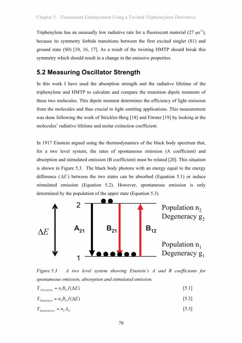
Chapter 5 – Fluorescent Enhancement Using a Twisted Tripheneylene Derivative
78
Triphenylene has an unusually low radiative rate for a fluorescent material (27 µs-1),
because its symmetry forbids transitions between the first excited singlet (S1) and
ground state (S0) [10, 16, 17]. As a result of the twisting HMTP should break this
symmetry which should result in a change in the emissive properties.
5.2 Measuring Oscillator Strength In this work I have used the absorption strength and the radiative lifetime of the
triphenylene and HMTP to calculate and compare the transition dipole moments of
these two molecules. This dipole moment determines the efficiency of light emission
from the molecules and thus crucial to light emitting applications. This measurement
was done following the work of Strickler-Berg [18] and Förster [19] by looking at the
molecules’ radiative lifetime and molar extinction coefficient.
In 1917 Einstein argued using the thermodynamics of the black body spectrum that,
for a two level system, the rates of spontaneous emission (A coefficient) and
absorption and stimulated emission (B coefficient) must be related [20]. This situation
is shown in Figure 5.3. The black body photons with an energy equal to the energy
difference ( E∆ ) between the two states can be absorbed (Equation 5.1) or induce
stimulated emission (Equation 5.2). However, spontaneous emission is only
determined by the population of the upper state (Equation 5.3).
2
1
Population n2
Degeneracy g2
Population n1
Degeneracy g1
E∆ A21 B21 B12
Figure 5.3 A two level system showing Einstein’s A and B coefficients for
spontaneous emission, absorption and stimulated emission.
)(121 EIBnAbsorption ∆=Γ [5.1]
)(212 EIBnStimulated ∆=Γ [5.2]
212 AnusSpontainio =Γ [5.3]
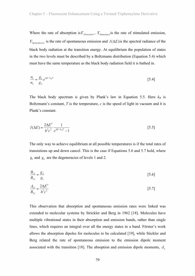
Chapter 5 – Fluorescent Enhancement Using a Twisted Tripheneylene Derivative
79
Where the rate of absorption is AbsorptionΓ , StimulatedΓ is the rate of stimulated emission,
usSpontainioΓ is the rate of spontaneous emission and )( EI ∆ is the spectral radiance of the
black body radiation at the transition energy. At equilibrium the population of states
in the two levels must be described by a Boltzmann distribution (Equation 5.4) which
must have the same temperature as the black body radiation field it is bathed in.
TkE Begg
nn /
2
1
2
1 ∆= [5.4]
The black body spectrum is given by Plank’s law in Equation 5.5. Here kB is
Boltzmann’s constant, T is the temperature, c is the speed of light in vacuum and h is
Plank’s constant.
1
12)(
/22
3
−
∆=∆
∆ TkE BechEEI [5.5]
The only way to achieve equilibrium at all possible temperatures is if the total rates of
transistions up and down cancel. This is the case if Equations 5.6 and 5.7 hold, where
g1 and g2 are the degeneracies of levels 1 and 2.
1
2
21
12
gg
BB
= [5.6]
22
3
21
21 2
chE
BA ∆
= [5.7]
This observation that absorption and spontaneous emission rates were linked was
extended to molecular systems by Strickler and Berg in 1962 [18]. Molecules have
multiple vibrational states in their absorption and emission bands, rather than single
lines, which requires an integral over all the energy states in a band. Förster’s work
allows the absorption dipoles for molecules to be calculated [19], while Stickler and
Berg related the rate of spontaneous emission to the emission dipole moment
associated with the transition [18]. The absoption and emission dipole moments, ad

Chapter 5 – Fluorescent Enhancement Using a Twisted Tripheneylene Derivative
80
and ed respectively, are calculated below following Equations 5.8 and 5.9. The dipole
moments are expressed in units of Debye (D). One Debye is 3.33564 × 10⁻³⁰ Cm. The
absorption dipole moment is calculated using the integrated molar extinction
coefficient spectrum )~(νε in M-1cm-1 integrated over photon energy in units of
wavenumber in cm-1 (ν~ ) and the local refractive index n.
∫−×= νννε ~~
)~(10186.9 32 dnda [5.8]
The emission dipole moment ed is calculated using the radiative lifetime Rτ in
seconds and the emission spectrum versus energy in photons per joule )(EI . Here 0ε
is the electric permittivity of free space in Fm-1, c is the speed of light in ms-1 and � is
the reduced Planck’s constant in J s.
( )R
e n
dEEIdEEIEcd
τ
πε30-
33402
103.33564
)(/)(3
×= ∫ ∫−�
[5.9]
Stickler and Berg note that their formula can only be expected to provide the same
dipole moment in absorption and emission in cases where the molecule does not
significantly change shape in the excited state, as this would obviously affect the
dipole moments. They also note that their calculations make use of an assumption that
the transitions are strongly allowed, unlike those in triphenylene. However as I am
only aiming to compare the relative strengths of dipole moments of HMTP and
triphenylene rather than provide exact values, these equations should be sufficient.
The measured photoluminescence quantum yield and transient luminescence are
direct measures of the emissive properties of the molecule and can still be used to
compare molecules’ emissive properties in the weakly allowed or forbidden regime.
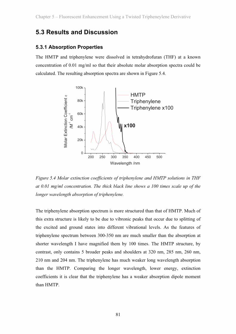
Chapter 5 – Fluorescent Enhancement Using a Twisted Tripheneylene Derivative
81
5.3 Results and Discussion
5.3.1 Absorption Properties
The HMTP and triphenylene were dissolved in tetrahydrofuran (THF) at a known
concentration of 0.01 mg/ml so that their absolute molar absorption spectra could be
calculated. The resulting absorption spectra are shown in Figure 5.4.
200 250 300 350 400 450 5000
20k
40k
60k
80k
100k
x100
Mo
lar
Extin
ctio
n C
oe
ffic
ien
t ε
/M-1 c
m-1
Wavelength /nm
HMTP
Triphenylene
Triphenylene x100
Figure 5.4 Molar extinction coefficients of triphenylene and HMTP solutions in THF
at 0.01 mg/ml concentration. The thick black line shows a 100 times scale up of the
longer wavelength absorption of triphenylene.
The triphenylene absorption spectrum is more structured than that of HMTP. Much of
this extra structure is likely to be due to vibronic peaks that occur due to splitting of
the excited and ground states into different vibrational levels. As the features of
triphenylene spectrum between 300-350 nm are much smaller than the absorption at
shorter wavelength I have magnified them by 100 times. The HMTP structure, by
contrast, only contains 5 broader peaks and shoulders at 320 nm, 285 nm, 260 nm,
210 nm and 204 nm. The triphenylene has much weaker long wavelength absorption
than the HMTP. Comparing the longer wavelength, lower energy, extinction
coefficients it is clear that the triphenylene has a weaker absorption dipole moment
than HMTP.
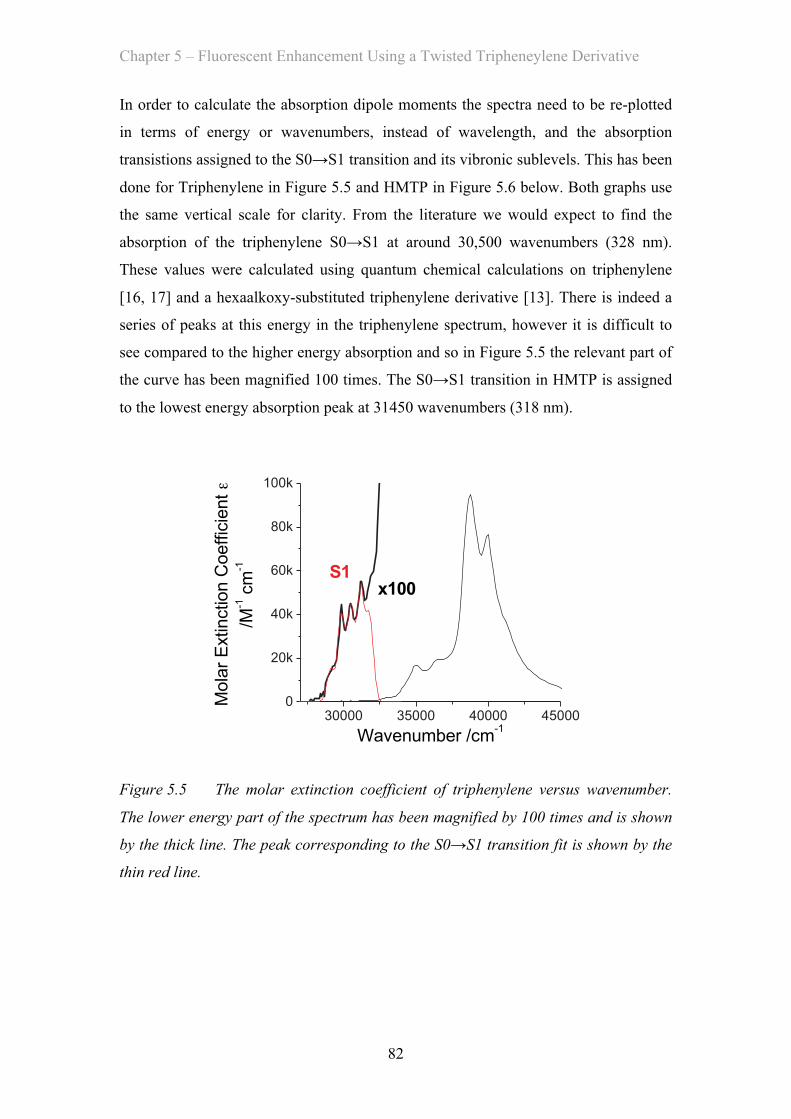
Chapter 5 – Fluorescent Enhancement Using a Twisted Tripheneylene Derivative
82
In order to calculate the absorption dipole moments the spectra need to be re-plotted
in terms of energy or wavenumbers, instead of wavelength, and the absorption
transistions assigned to the S0→S1 transition and its vibronic sublevels. This has been
done for Triphenylene in Figure 5.5 and HMTP in Figure 5.6 below. Both graphs use
the same vertical scale for clarity. From the literature we would expect to find the
absorption of the triphenylene S0→S1 at around 30,500 wavenumbers (328 nm).
These values were calculated using quantum chemical calculations on triphenylene
[16, 17] and a hexaalkoxy-substituted triphenylene derivative [13]. There is indeed a
series of peaks at this energy in the triphenylene spectrum, however it is difficult to
see compared to the higher energy absorption and so in Figure 5.5 the relevant part of
the curve has been magnified 100 times. The S0→S1 transition in HMTP is assigned
to the lowest energy absorption peak at 31450 wavenumbers (318 nm).
30000 35000 40000 450000
20k
40k
60k
80k
100k
S1x100
Mola
r E
xtinction C
oeffic
ient ε
/M-1 c
m-1
Wavenumber /cm-1
Figure 5.5 The molar extinction coefficient of triphenylene versus wavenumber.
The lower energy part of the spectrum has been magnified by 100 times and is shown
by the thick line. The peak corresponding to the S0→S1 transition fit is shown by the
thin red line.
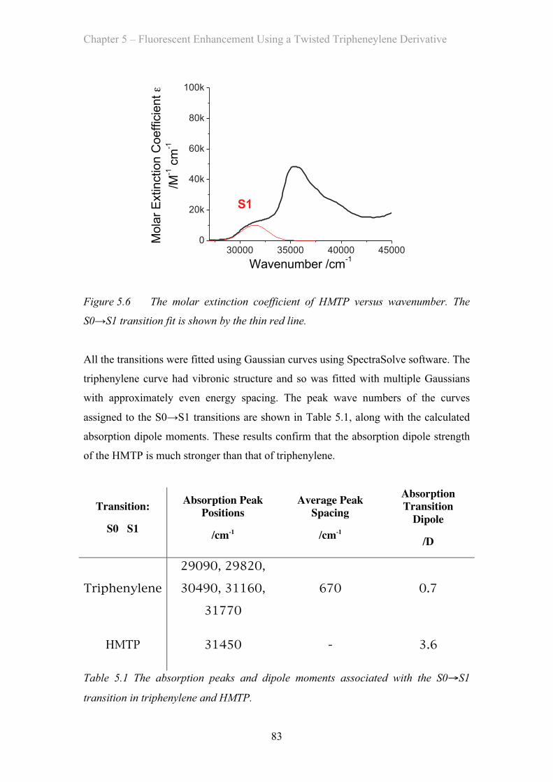
Chapter 5 – Fluorescent Enhancement Using a Twisted Tripheneylene Derivative
83
30000 35000 40000 450000
20k
40k
60k
80k
100k
S1
Mola
r E
xtinction C
oeffic
ient ε
/M-1 c
m-1
Wavenumber /cm-1
Figure 5.6 The molar extinction coefficient of HMTP versus wavenumber. The
S0→S1 transition fit is shown by the thin red line.
All the transitions were fitted using Gaussian curves using SpectraSolve software. The
triphenylene curve had vibronic structure and so was fitted with multiple Gaussians
with approximately even energy spacing. The peak wave numbers of the curves
assigned to the S0→S1 transitions are shown in Table 5.1, along with the calculated
absorption dipole moments. These results confirm that the absorption dipole strength
of the HMTP is much stronger than that of triphenylene.
Transition:
S0 S1
Absorption Peak Positions
/cm-1
Average Peak Spacing
/cm-1
Absorption Transition
Dipole
/D
Triphenylene
29090, 29820,
30490, 31160,
31770
670 0.7
HMTP 31450 - 3.6
Table 5.1 The absorption peaks and dipole moments associated with the S0→S1
transition in triphenylene and HMTP.
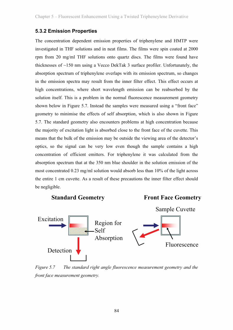
Chapter 5 – Fluorescent Enhancement Using a Twisted Tripheneylene Derivative
84
5.3.2 Emission Properties
The concentration dependent emission properties of triphenylene and HMTP were
investigated in THF solutions and in neat films. The films were spin coated at 2000
rpm from 20 mg/ml THF solutions onto quartz discs. The films were found have
thicknesses of ~150 nm using a Vecco DekTak 3 surface profiler. Unfortunately, the
absorption spectrum of triphenylene overlaps with its emission spectrum, so changes
in the emission spectra may result from the inner filter effect. This effect occurs at
high concentrations, where short wavelength emission can be reabsorbed by the
solution itself. This is a problem in the normal fluorescence measurement geometry
shown below in Figure 5.7. Instead the samples were measured using a “front face”
geometry to minimise the effects of self absorption, which is also shown in Figure
5.7. The standard geometry also encounters problems at high concentration because
the majority of excitation light is absorbed close to the front face of the cuvette. This
means that the bulk of the emission may be outside the viewing area of the detector’s
optics, so the signal can be very low even though the sample contains a high
concentration of efficient emitters. For triphenylene it was calculated from the
absorption spectrum that at the 350 nm blue shoulder in the solution emission of the
most concentrated 0.23 mg/ml solution would absorb less than 10% of the light across
the entire 1 cm cuvette. As a result of these precautions the inner filter effect should
be negligible.
Region for Self Absorption
Standard Geometry Front Face Geometry
Excitation
Detection
Sample Cuvette
Fluorescence
Figure 5.7 The standard right angle fluorescence measurement geometry and the
front face measurement geometry.
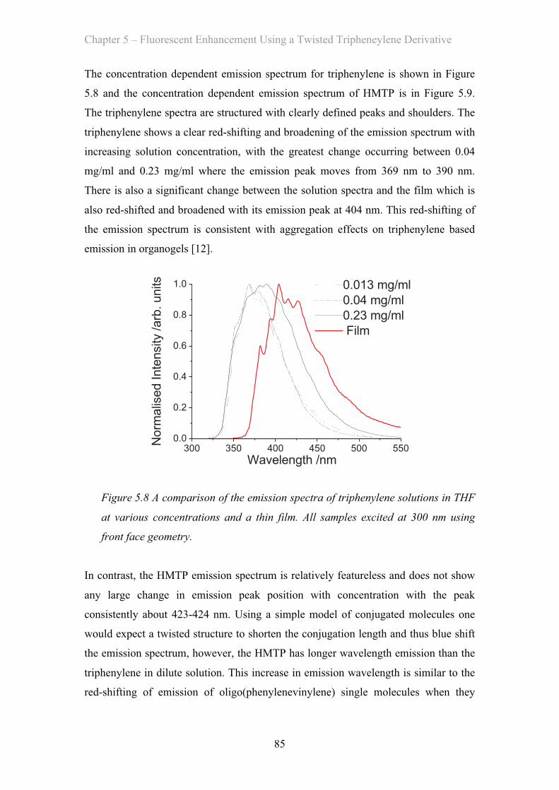
Chapter 5 – Fluorescent Enhancement Using a Twisted Tripheneylene Derivative
85
The concentration dependent emission spectrum for triphenylene is shown in Figure
5.8 and the concentration dependent emission spectrum of HMTP is in Figure 5.9.
The triphenylene spectra are structured with clearly defined peaks and shoulders. The
triphenylene shows a clear red-shifting and broadening of the emission spectrum with
increasing solution concentration, with the greatest change occurring between 0.04
mg/ml and 0.23 mg/ml where the emission peak moves from 369 nm to 390 nm.
There is also a significant change between the solution spectra and the film which is
also red-shifted and broadened with its emission peak at 404 nm. This red-shifting of
the emission spectrum is consistent with aggregation effects on triphenylene based
emission in organogels [12].
300 350 400 450 500 5500.0
0.2
0.4
0.6
0.8
1.0
Norm
alis
ed Inte
nsity /arb
. units
Wavelength /nm
0.013 mg/ml
0.04 mg/ml
0.23 mg/ml
Film
Figure 5.8 A comparison of the emission spectra of triphenylene solutions in THF
at various concentrations and a thin film. All samples excited at 300 nm using
front face geometry.
In contrast, the HMTP emission spectrum is relatively featureless and does not show
any large change in emission peak position with concentration with the peak
consistently about 423-424 nm. Using a simple model of conjugated molecules one
would expect a twisted structure to shorten the conjugation length and thus blue shift
the emission spectrum, however, the HMTP has longer wavelength emission than the
triphenylene in dilute solution. This increase in emission wavelength is similar to the
red-shifting of emission of oligo(phenylenevinylene) single molecules when they
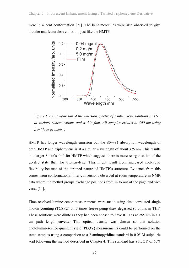
Chapter 5 – Fluorescent Enhancement Using a Twisted Tripheneylene Derivative
86
were in a bent conformation [21]. The bent molecules were also observed to give
broader and featureless emission, just like the HMTP.
300 350 400 450 500 5500.0
0.2
0.4
0.6
0.8
1.0
Norm
alis
ed Inte
nsity /arb
. units
Wavelength /nm
0.04 mg/ml
0.2 mg/ml
5.0 mg/ml
Film
Figure 5.9 A comparison of the emission spectra of triphenylene solutions in THF
at various concentrations and a thin film. All samples excited at 300 nm using
front face geometry.
HMTP has longer wavelength emission but the S0→S1 absorption wavelength of
both HMTP and triphenylene is at a similar wavelength of about 325 nm. This results
in a larger Stoke’s shift for HMTP which suggests there is more reorganisation of the
excited state than for triphenylene. This might result from increased molecular
flexibility because of the strained nature of HMTP’s structure. Evidence from this
comes from conformational inter-conversions observed at room temperature in NMR
data where the methyl groups exchange positions from in to out of the page and vice
versa [14].
Time-resolved luminescence measurements were made using time-correlated single
photon counting (TCSPC) on 3 times freeze-pump-thaw degassed solutions in THF.
These solutions were dilute as they had been chosen to have 0.1 abs at 285 nm in a 1
cm path length cuvette. This optical density was chosen so that solution
photoluminescence quantum yield (PLQY) measurements could be performed on the
same samples using a comparison to a 2-aminopyridine standard in 0.05 M sulphuric
acid following the method described in Chapter 4. This standard has a PLQY of 60%

Chapter 5 – Fluorescent Enhancement Using a Twisted Tripheneylene Derivative
87
when excited at 285 nm [22]. Using the molar extinction coefficients this results in a
concentration of 0.0014 mg/ml for triphenylene and 0.00065 mg/ml for HMTP. These
concentrations are much lower than the point at which concentration dependent
effects were observed in the triphenylene emission spectrum.
These samples were also compared to neat films spin coated under the same
conditions as above. These samples were measured in vacuum. The samples were
excited at 266 nm using twice frequency doubled Nd:YAG laser giving an instrument
response function of ~500 ps full width half maximum. The results from the
triphenylene solution and film are shown in Figure 5.10 and the results from the
HMTP solution and film were shown in Figure 5.11.
0 10 20 30 40 50 60 70 800.01
0.1
1
Norm
alis
ed Inte
nsity
Time /ns
Figure 5.10 Triphenylene Time-resolved luminescence in solution (red open
circles, black fit line) and film (black filled squares, red fit line). Samples were excited
at 266 nm and the emission detected at 390 nm.
The triphenylene fluorescence decays are not straight lines on the log plot and so are
not well fitted by a single exponential decay. This indicates that the samples contain
multiple emissive environments, even in the dilute solution. By contrast HMTP shows
single exponential decays in solution, film and powder indicating only one emissive
state is present in both solution and solid samples.
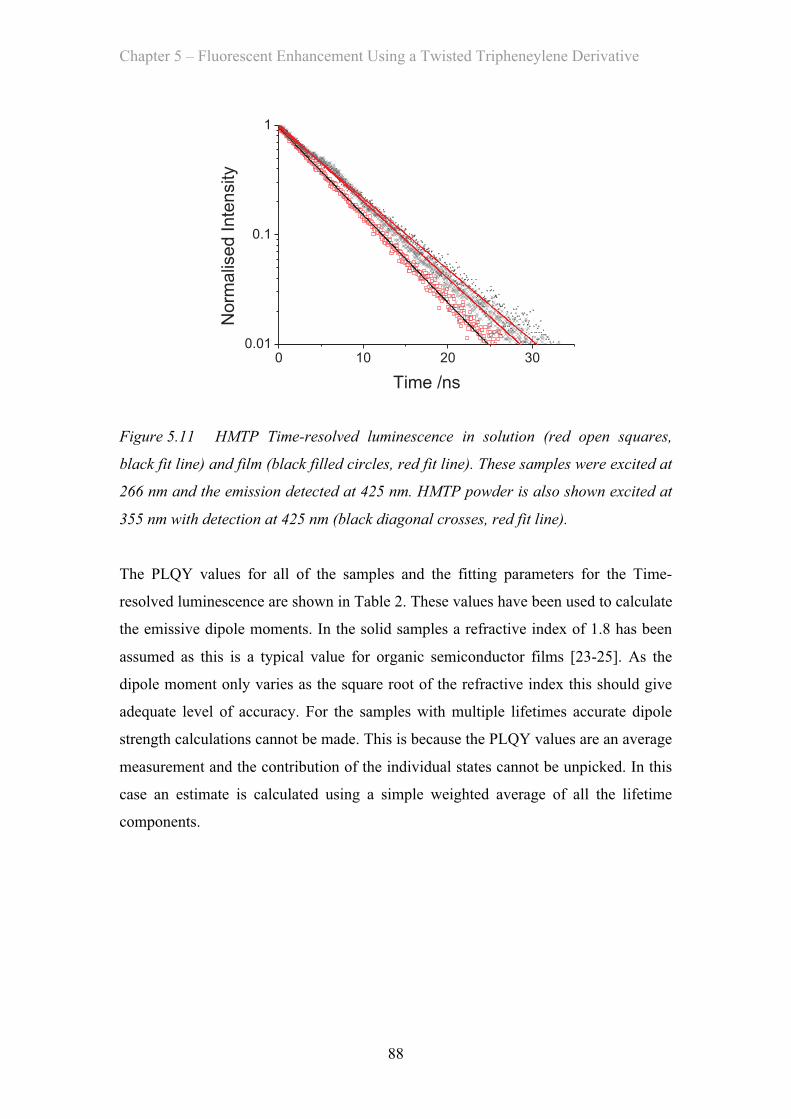
Chapter 5 – Fluorescent Enhancement Using a Twisted Tripheneylene Derivative
88
0 10 20 300.01
0.1
1
Norm
alis
ed Inte
nsity
Time /ns
Figure 5.11 HMTP Time-resolved luminescence in solution (red open squares,
black fit line) and film (black filled circles, red fit line). These samples were excited at
266 nm and the emission detected at 425 nm. HMTP powder is also shown excited at
355 nm with detection at 425 nm (black diagonal crosses, red fit line).
The PLQY values for all of the samples and the fitting parameters for the Time-
resolved luminescence are shown in Table 2. These values have been used to calculate
the emissive dipole moments. In the solid samples a refractive index of 1.8 has been
assumed as this is a typical value for organic semiconductor films [23-25]. As the
dipole moment only varies as the square root of the refractive index this should give
adequate level of accuracy. For the samples with multiple lifetimes accurate dipole
strength calculations cannot be made. This is because the PLQY values are an average
measurement and the contribution of the individual states cannot be unpicked. In this
case an estimate is calculated using a simple weighted average of all the lifetime
components.
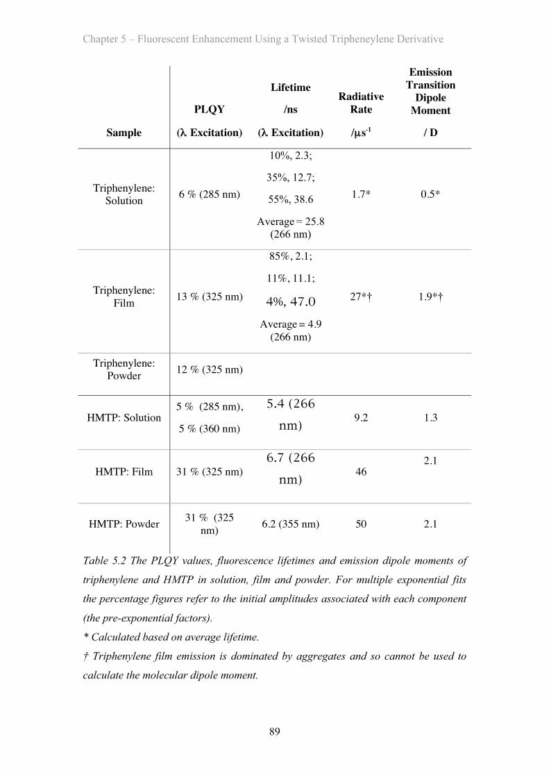
Chapter 5 – Fluorescent Enhancement Using a Twisted Tripheneylene Derivative
89
Sample
PLQY
(λλ Excitation)
Lifetime
/ns
(λλ Excitation)
Radiative Rate
/µµs-1
Emission Transition
Dipole Moment
/ D
Triphenylene: Solution
6 % (285 nm)
10%, 2.3;
35%, 12.7;
55%, 38.6
Average = 25.8 (266 nm)
1.7* 0.5*
Triphenylene: Film
13 % (325 nm)
85%, 2.1;
11%, 11.1;
4%, 47.0
Average = 4.9 (266 nm)
27*† 1.9*†
Triphenylene: Powder
12 % (325 nm)
HMTP: Solution 5 % (285 nm),
5 % (360 nm)
5.4 (266
nm) 9.2 1.3
HMTP: Film 31 % (325 nm) 6.7 (266
nm) 46
2.1
HMTP: Powder 31 % (325
nm) 6.2 (355 nm) 50 2.1
Table 5.2 The PLQY values, fluorescence lifetimes and emission dipole moments of
triphenylene and HMTP in solution, film and powder. For multiple exponential fits
the percentage figures refer to the initial amplitudes associated with each component
(the pre-exponential factors).
* Calculated based on average lifetime.
† Triphenylene film emission is dominated by aggregates and so cannot be used to
calculate the molecular dipole moment.
Chapter 5 – Fluorescent Enhancement Using a Twisted Tripheneylene Derivative
90
The concentration dependence of triphenylene emission and the multiple emissive
states that appear in Time-resolved luminescence both suggest that the triphenylene is
π stacking, even in dilute solution, and forming aggregates. X-ray diffraction data
shows that HMTP does not π stack in the solid state [14] and this is consistent with
the fact that HMTP does not show concentration dependence in solution, and even in
the solid state only one emissive state is present.
In dilute solution, where aggregation should not play a significant role, the PLQYs of
HMTP (5%) and triphenylene (6%) are comparable but the HMTP has a much shorter
lifetime (5.4 ns compared to an average lifetime of 25.8 ns). This shows that the
HMTP has a higher radiative rate, and because the emission energies are not too
different, this indicates a higher emission dipole moment than triphenylene. This
confirms the results that the absorption dipole is higher in HMTP than triphenylene.
Both the HMTP and triphenylene films show increased PLQY compared to the
solutions. This is unusual, as normally concentration quenching reduces luminescence
in the solid state. In triphenylene the PLQY increases from 6% to 13% in film and this
is accompanied by a decrease in the emission lifetime indicating that there is an
increase in the radiative rate. As we would expect the solid state to contain π stacked
aggregates this appears to be a case of aggregate enhanced emission [2]. This could be
due to the fact that the isolated triphenylene molecule’s symmetry is what prevents
light emission. Aggregates offer a way in which this symmetry could be broken
resulting in greater light emission efficiency.
When calculating the solution dipole moment for the triphenylene an average lifetime
has been used, however, lifetime data from the literature gives a fluorescence lifetime
of about 40 ns [17, 26]. This is a close match to the 55% 38.6 ns component present in
dilute solution and so this component is likely to correspond to the monomer. If this
~40 ns lifetime is used to calculate the emission dipole moment then it decreases
slightly from 0.5 D to 0.4 D. Both values are consistent with the solution absorption
dipole moment of 0.7 D.
Chapter 5 – Fluorescent Enhancement Using a Twisted Tripheneylene Derivative
91
HMTP’s enhancement in PLQY is more dramatic as it increases from 5% to 31% in
film. In HMTP there is only one exponential component in both solution and film
indicating that there is only one emissive state, and making aggregation induced
changes to the emissive properties unlikely. The lifetime of the HMTP in solution is
5.4 ns, which is shorter than in film (6.7 ns) or powder (6.2 ns). This could imply that
the increased PLQY in film is due to a reduced non-radiative de-excitation rate. This
could happen if the HMTP molecule could de-excite through molecular vibrations
which are prevented in the solid state [27]. An example of the kinds of vibrations that
are possible are the conformational inter-conversion that HMTP undergoes [14]. This
could offer an increased non-radiative pathway in the solution state for excitations to
decay that would be blocked in the solid state by the rigid framework provided by the
neighbouring molecules. Unfortunately an increased non-radiative rate does not
suffice as an explanation, as the change in lifetime is too small to account for the
change in PLQY by itself. This can be seen in the fact that HMTP solutions and films
have significantly different calculated radiative rates in Table 5.2.
It is possible that in solution some of the HMTP molecules adopt different
conformations or transition states that are capable of absorption but do not emit light.
This would cause a lowering of the measured PLQY as photons would be absorbed by
these conformers without emitting light, apparently increasing the number of absorbed
photons for each one emitted. This hypothesis would also explain that while the
absorption and emission dipole moments for triphenylene are similar (0.7 D and 0.5
D) in dilute solution they are significantly different in HMTP (3.6 D and 1.3 D). The
lower emission dipole moment could be explained if I were including non-emissive
conformers in my calculation. This is because the reduced PLQY reduces the radative
rate, which is used in the calculation of the emission dipole. The film emission dipole
moment of HMTP is 2.1 D, closer to the absorption value and so perhaps offers a
better model for the isolated HMTP molecule in the C2 conformation shown in Figure
5.1. This suggests that dark conformers are a likely explanation for the anomalously
low solution PLQY in HMTP.
Chapter 5 – Fluorescent Enhancement Using a Twisted Tripheneylene Derivative
92
5.4 OLED Measurements
OLED measurements of neat HMTP films ~100 nm were attempted using a single
layer structure however the material was found to be insulating. The films also
crystalised within a short time after being spin cast resulting in significant film
roughness that would be deleterious to device performance. OLEDs were also
attempted using 20 wt% of HMTP in a host of 4,4’-N,N’-dicarbazolyl-biphenyl (CBP)
to try and improve charge transport and prevent crystalisation however the performance
of these devices was extremely low and the electroluminescence spectrum did not
correspond to HMTP’s photoluminescence spectrum. By comparing the emission
spectrum of these devices to devices made with neat CBP it was determined that the
HMTP was resulting in significant changes in the emission spectrum and so the emission
in the blended device could not be ascribed to CBP alone.
5.5 Conclusion By comparing the triphenylene dilute solution measurement (which contains the
fewest aggregates) and the HMTP film measurement (which is not affected by non-
emissive conformers) we conclude that breaking the triphenylene symmetry has
meant the S1→S0 transition is no longer forbidden. This means the twisted HMTP
molecule has a dipole moment by ~4 times greater and radiative rate ~20 times faster
than triphenylene.
The twisted structure of HMTP also prevents π stacking and thus aggregation in the
solid state. This can be seen from the fact that the concentration dependence of
triphenylene’s emission spectrum has been eliminated in HMTP, and single lifetime
fluorescence decay from HMTP solution and films show a single emissive state.
Together, with the increased oscillator strength this resulted in efficient luminescence
from HMTP films with a photoluminescence quantum yield of 31%.
The PLQY of HMTP in films and powder is 6 times as high as in the solution. This
difference is explained partially by an increased non-radiative rate in solution, but the
main part of this difference is assigned to the presence of dark conformers within the
solution, which contribute to the absorption but do not emit light.
Chapter 5 – Fluorescent Enhancement Using a Twisted Tripheneylene Derivative
93
Overall the results show that twisting molecules out of one plane is an effective
strategy for eliminating intermolecular interactions, and producing efficient emissive
materials.
1. Melhuish, W.H., Quantum Efficiencies of Fluorescence of Organic Substances: Effect of Solvent and Concentration on the Fluorescent Solute. Journal of Physical Chemistry, 1961. 65: p. 229.
2. Hong, Y.N., J.W.Y. Lam, and B.Z. Tang, Aggregation-induced emission: phenomenon, mechanism and applications. Chemical Communications, 2009(29): p. 4332-4353.
3. Schouwink, P., et al., The influence of molecular aggregation on the device properties of organic light emitting diodes. Thin Solid Films, 2000. 372(1-2): p. 163-168.
4. Setayesh, S., et al., Polyfluorenes with polyphenylene dendron side chains: Toward non-aggregating, light-emitting polymers. Journal of the American Chemical Society, 2001. 123(5): p. 946-953.
5. Gambino, S., A.K. Bansal, and I.D.W. Samuel, Comparison of hole mobility in thick and thin films of a conjugated polymer. Organic Electronics, 2010. 11(3): p. 467-471.
6. Burn, P.L., S.C. Lo, and I.D.W. Samuel, The development of light-emitting dendrimers for displays. Advanced Materials, 2007. 19(13): p. 1675-1688.
7. Lo, S.C., et al., Green phosphorescent dendrimer for light-emitting diodes. Advanced Materials, 2002. 14(13-14): p. 975.
8. Lo, S.C., et al., Encapsulated cores: Host-free organic light-emitting diodes based on solution-processible electrophosphorescent dendrimers. Advanced Materials, 2005. 17(16): p. 1945-+.
9. Salbeck, J., et al., Low molecular organic glasses for blue electroluminescence. Synthetic Metals, 1997. 91(1-3): p. 209-215.
10. Markovitsi, D., et al., Triphenylene Columnar Liquid-Crystals - Excited States and Energy Transfer. Journal of Physical Chemistry, 1995. 99(3): p. 1005-1017.
11. McKenna, M.D., et al., Discotic liquid crystalline poly(propylene imine) dendrimers based on triphenylene. Journal of the American Chemical Society, 2005. 127(2): p. 619-625.
12. Ikeda, M., M. Takeuchi, and S. Shinkai, Unusual emission properties of a triphenylene-based organogel system. Chemical Communications, 2003(12): p. 1354-1355.
13. Markovitsi, D., et al., Triplet excitation transfer in triphenylene columnar phases. Journal of Physical Chemistry B, 2001. 105(7): p. 1299-1306.
14. Wang, Y., et al., 1,4,5,8,9,12-hexamethyltriphenylene. A molecule with a flipping twist. Journal of the American Chemical Society, 2007. 129(43): p. 13193-13200.
15. Ahmed, F.R. and J. Trotter, The Crystal Structure of Triphenylene. Acta Crystallographica, 1963. 16(6): p. 503-508.
16. Di Donato, E., et al., Tuning Fluorescence Lifetimes through Changes in Herzberg-Teller Activities: The Case of Triphenylene and Its Hexamethoxy-
Chapter 5 – Fluorescent Enhancement Using a Twisted Tripheneylene Derivative
94
Substituted Derivative. Journal of Physical Chemistry A, 2009. 113(23): p. 6504-6510.
17. Kokkin, D.L., et al., Gas phase spectra of all-benzenoid polycyclic aromatic hydrocarbons: Triphenylene. Journal of Chemical Physics, 2007. 126(8).
18. Strickler, S.J. and R.A. Berg, Relationship between absorption intensity and fluorescence lifetime of molecules. Journal of Chemical Physics, 1962. 37(4): p. 814.
19. Knox, R.S. and H. van Amerongen, Refractive index dependence of the Forster resonance excitation transfer rate. Journal of Physical Chemistry B, 2002. 106(20): p. 5289-5293.
20. Einstein, A., Zur Quantentheorie der Strahlung. Physikalische Zeitschrift, 1917. 18: p. 121-128.
21. Becker, K., et al., How chromophore shape determines the spectroscopy of phenylene-vinylenes: Origin of spectral broadening in the absence of aggregation. Journal of Physical Chemistry B, 2008. 112(16): p. 4859-4864.
22. Rusakowicz, R. and A.C. Testa, 2-Aminopyridine as a Standard for Low-Wavelength Spectrofluorimetry. Journal of Physical Chemistry, 1968. 72(7): p. 2680.
23. Liu, Z.T., et al., The characterization of the optical functions of BCP and CBP thin films by spectroscopic ellipsometry. Synthetic Metals, 2005. 150(2): p. 159-163.
24. Greenham, N.C., R.H. Friend, and D.D.C. Bradley, Angular-Dependance of the Emission From a Conjugated Polymer Light-Emitting Diode - Implications For Efficiency Calculations. Advanced Materials, 1994. 6(6): p. 491-494.
25. Khalfin, V.B., et al., Weak microcavity effects in organic light-emitting devices. 1998. - 58(- 7).
26. Wallace, W.L., R.P. Vanduyne, and F.D. Lewis, Quenching of Aromatic Hydrocarbon Singlets and Aryl Ketone Triplets by Alkyl Disulfides. Journal of the American Chemical Society, 1976. 98(17): p. 5319-5326.
27. Harding, R.E., et al., Non-radiative decay mechanisms in blue phosphorescent iridium(III) complexes. Organic Electronics, 2008. 9(3): p. 377-384.
95
6. Poly(dendrimer) Iridium Complexes
6.1 Introduction ............................................................................................................ 95�6.2 Introduction to Phosphorescent Polymers ............................................................. 96�6.3 Ir(ppy)2(acac) Based Polymers .............................................................................. 97�
6.3.1 Ir(ppy)2(acac) Solution Properties .............................................................. 98�6.3.2 Ir(ppy)2(acac) Film Properties .................................................................. 101�6.3.3 Dendronised Ir(ppy)2(acac) Polymer Properties ....................................... 102�
6.4 Ir(ppy)2(ptz) Based Poly(Dendrimers) ................................................................. 106�6.4.1 Ir(ppy)2(ptz) Solution Properties ............................................................... 106�6.4.2 Ir(ppy)2(ptz) Film Properties ..................................................................... 108�6.4.3 Ir(ppy)2(ptz) OLED Devices ..................................................................... 109�
6.5 Doubly Dendronised Ir(ppy)2(ptz) Polymer ........................................................ 112�6.6.1 Double Dendron Solution Properties ........................................................ 113�6.5.2 Double Dendron Film Properties .............................................................. 115�6.5.3 Double Dendron OLED Devices .............................................................. 116�
6.6 Summary of Materials .......................................................................................... 119�6.7 Conclusions .......................................................................................................... 119�
6.1 Introduction
In this chapter I overview the work that was done on iridum polymers for solution
processable phosphorescent organic light emitting diodes. An introduction to
phosphorescent polymers is given in Section 6.2 and experimental results are given in
Sections 6.3, 6.4 and 6.5. Section 6.3 contains early work using Ir(ppy)2(acac) based
polymers with and without dendrons to control aggregation in thin films. Section 6.4
covers work using the higher luminescent efficiency Ir(ppy)2(ptz) based
polymer(dendrimer) and Section 6.5 discusses a poly(dendrimer) that uses double
dendrons to better protect the cores from aggregation in the solid state and achieve
higher efficiencies. A summary of all the materials used in this chapter is given in
Section 6.6. Finally the conclusions are presented in Section 6.7.
Chapter 6 – Poly(dendrimer) Iridium Complexes
96
6.2 Introduction to Phosphorescent Polymers
Much work has been done on the small molecule iridium complexes like fac-tris(2-
phenylpyridine) iridium(III) or Ir(ppy)3 which emits in the green [1, 2] for
phosphorescent OLEDs. Typically these materials are deposited by thermal
evaporation. Unfortunately, this technique is relatively costly and slow as it requires
high vacuum but these small molecules are only slightly soluble in organic solvents
and so are difficult to process via solution. In addition, solution processing can lead to
aggregate formation in these materials as the molecules have more chance to order
than if they are deposited into a glassy phase via thermal deposition.
Conjugated polymers, on the other hand, are readily solution processable. However
they are not generally phosphorescent and so have limited maximum efficiencies in
devices. This failing lead to the development of dendrimers, discussed in Chapter 3,
with phosphorescent cores to provide a route to low cost highly efficient OLEDs.
These devices have achieved 16% external quantum efficiency or ~80% internal
quantum efficiency [3]. Unfortunately, unlike a polymer, dendrimers do not
significantly modify the viscosity of their solvent when dissolved [4, 5]. These higher
viscosities are required for ink-jet printing [6-8], which in turn allows patterned
deposition of OLED materials that is required to produce a colour display. To
overcome this limitation the idea of this project was to investigate phosphorescent
poly(dendrimers) for use in OLEDs. The materials for this project were synthesised
and chemically characterised by Wen-Yong Lai, Shih-Chun Lo and Paul Burn at the
University of Queensland.
Phosphorescent polymers consist of two main components: the polymer backbone and
the pendant iridium complexes. In much previous work conjugated polymers like
poly(fluorene) have been used to provide the backbone [9-14]. Although the chosen
polymers may be blue emitters this colour comes from the singlet state of the
polymer. As the triplet state is lower lying this means that for green and blue emitting
pendant iridium complexes back transfer to the polymer backbone often occurs,
limiting the efficiency of devices [13-15]. These effects are illustrated in Figure 6.1.
Though this problem is particularly pronounced in Poly(fluorene) due to the large
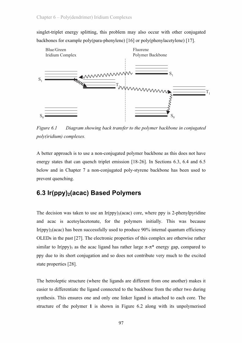
Chapter 6 – Poly(dendrimer) Iridium Complexes
97
singlet-triplet energy splitting, this problem may also occur with other conjugated
backbones for example poly(para-phenylene) [16] or poly(phenylacetylene) [17].
T1
S1
S0
FluorenePolymer Backbone
Blue/GreenIridium Complex
T1
S1
S0
Figure 6.1 Diagram showing back transfer to the polymer backbone in conjugated
poly(iridium) complexes.
A better approach is to use a non-conjugated polymer backbone as this does not have
energy states that can quench triplet emission [18-26]. In Sections 6.3, 6.4 and 6.5
below and in Chapter 7 a non-conjugated poly-styrene backbone has been used to
prevent quenching.
6.3 Ir(ppy)2(acac) Based Polymers
The decision was taken to use an Ir(ppy)2(acac) core, where ppy is 2-phenylpyridine
and acac is acetoylacetonate, for the polymers initially. This was because
Ir(ppy)2(acac) has been successfully used to produce 90% internal quantum efficiency
OLEDs in the past [27]. The electronic properties of this complex are otherwise rather
similar to Ir(ppy)3 as the acac ligand has rather large π-π* energy gap, compared to
ppy due to its short conjugation and so does not contribute very much to the excited
state properties [28].
The hetroleptic structure (where the ligands are different from one another) makes it
easier to differentiate the ligand connected to the backbone from the other two during
synthesis. This ensures one and only one linker ligand is attached to each core. The
structure of the polymer 1 is shown in Figure 6.2 along with its unpolymerised
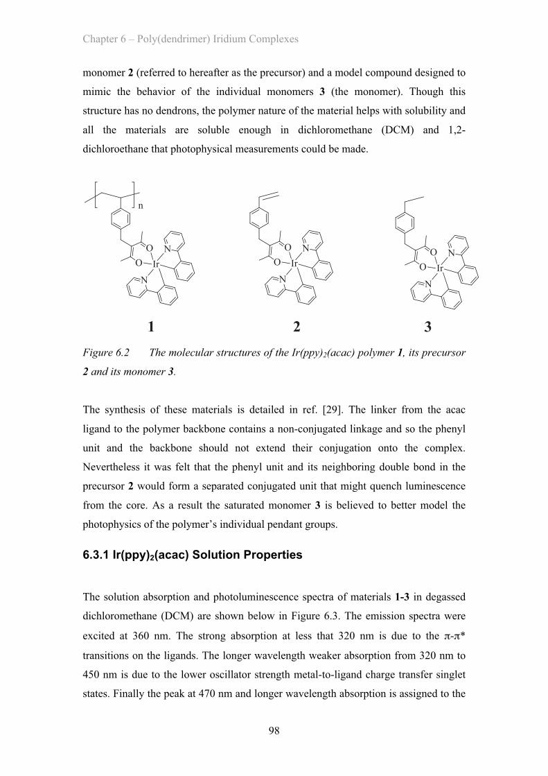
Chapter 6 – Poly(dendrimer) Iridium Complexes
98
monomer 2 (referred to hereafter as the precursor) and a model compound designed to
mimic the behavior of the individual monomers 3 (the monomer). Though this
structure has no dendrons, the polymer nature of the material helps with solubility and
all the materials are soluble enough in dichloromethane (DCM) and 1,2-
dichloroethane that photophysical measurements could be made.
1 2 3
Figure 6.2 The molecular structures of the Ir(ppy)2(acac) polymer 1, its precursor
2 and its monomer 3.
The synthesis of these materials is detailed in ref. [29]. The linker from the acac
ligand to the polymer backbone contains a non-conjugated linkage and so the phenyl
unit and the backbone should not extend their conjugation onto the complex.
Nevertheless it was felt that the phenyl unit and its neighboring double bond in the
precursor 2 would form a separated conjugated unit that might quench luminescence
from the core. As a result the saturated monomer 3 is believed to better model the
photophysics of the polymer’s individual pendant groups.
6.3.1 Ir(ppy)2(acac) Solution Properties
The solution absorption and photoluminescence spectra of materials 1-3 in degassed
dichloromethane (DCM) are shown below in Figure 6.3. The emission spectra were
excited at 360 nm. The strong absorption at less that 320 nm is due to the π-π*
transitions on the ligands. The longer wavelength weaker absorption from 320 nm to
450 nm is due to the lower oscillator strength metal-to-ligand charge transfer singlet
states. Finally the peak at 470 nm and longer wavelength absorption is assigned to the
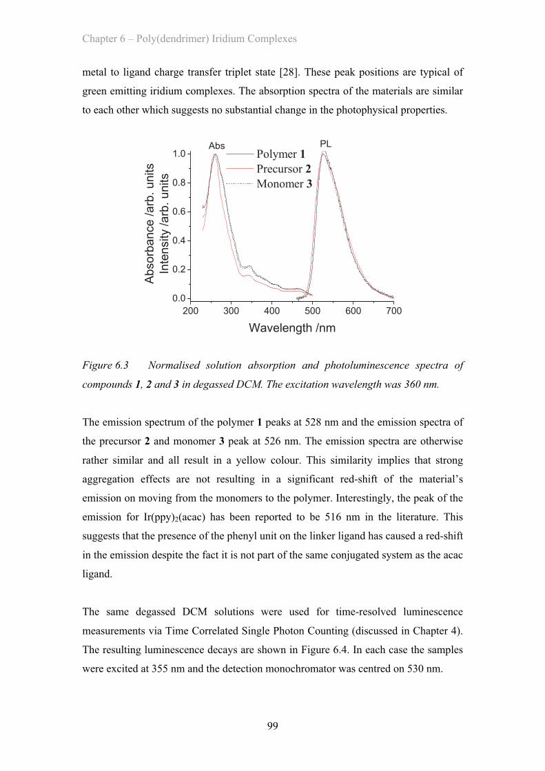
Chapter 6 – Poly(dendrimer) Iridium Complexes
99
metal to ligand charge transfer triplet state [28]. These peak positions are typical of
green emitting iridium complexes. The absorption spectra of the materials are similar
to each other which suggests no substantial change in the photophysical properties.
Figure 6.3 Normalised solution absorption and photoluminescence spectra of
compounds 1, 2 and 3 in degassed DCM. The excitation wavelength was 360 nm.
The emission spectrum of the polymer 1 peaks at 528 nm and the emission spectra of
the precursor 2 and monomer 3 peak at 526 nm. The emission spectra are otherwise
rather similar and all result in a yellow colour. This similarity implies that strong
aggregation effects are not resulting in a significant red-shift of the material’s
emission on moving from the monomers to the polymer. Interestingly, the peak of the
emission for Ir(ppy)2(acac) has been reported to be 516 nm in the literature. This
suggests that the presence of the phenyl unit on the linker ligand has caused a red-shift
in the emission despite the fact it is not part of the same conjugated system as the acac
ligand.
The same degassed DCM solutions were used for time-resolved luminescence
measurements via Time Correlated Single Photon Counting (discussed in Chapter 4).
The resulting luminescence decays are shown in Figure 6.4. In each case the samples
were excited at 355 nm and the detection monochromator was centred on 530 nm.
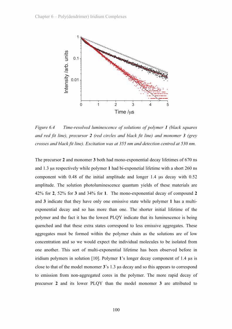
Chapter 6 – Poly(dendrimer) Iridium Complexes
100
0 1 2 3 4 5
0.01
0.1
1
Inte
nsity
/arb
. units
Time /µs
Figure 6.4 Time-resolved luminescence of solutions of polymer 1 (black squares
and red fit line), precursor 2 (red circles and black fit line) and monomer 3 (grey
crosses and black fit line). Excitation was at 355 nm and detection centred at 530 nm.
The precursor 2 and monomer 3 both had mono-exponential decay lifetimes of 670 ns
and 1.3 µs respectively while polymer 1 had bi-exponetial lifetime with a short 260 ns
component with 0.48 of the initial amplitude and longer 1.4 µs decay with 0.52
amplitude. The solution photoluminescence quantum yields of these materials are
42% for 2, 52% for 3 and 34% for 1. The mono-exponential decay of compound 2
and 3 indicate that they have only one emissive state while polymer 1 has a multi-
exponential decay and so has more than one. The shorter initial lifetime of the
polymer and the fact it has the lowest PLQY indicate that its luminescence is being
quenched and that these extra states correspond to less emissive aggregates. These
aggregates must be formed within the polymer chain as the solutions are of low
concentration and so we would expect the individual molecules to be isolated from
one another. This sort of multi-exponential lifetime has been observed before in
iridium polymers in solution [10]. Polymer 1’s longer decay component of 1.4 µs is
close to that of the model monomer 3’s 1.3 µs decay and so this appears to correspond
to emission from non-aggregated cores in the polymer. The more rapid decay of
precursor 2 and its lower PLQY than the model monomer 3 are attributed to
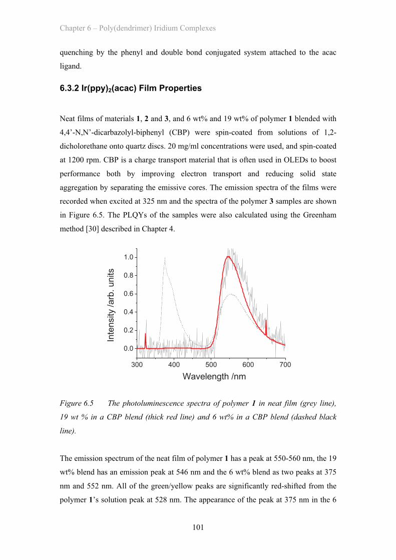
Chapter 6 – Poly(dendrimer) Iridium Complexes
101
quenching by the phenyl and double bond conjugated system attached to the acac
ligand.
6.3.2 Ir(ppy)2(acac) Film Properties
Neat films of materials 1, 2 and 3, and 6 wt% and 19 wt% of polymer 1 blended with
4,4’-N,N’-dicarbazolyl-biphenyl (CBP) were spin-coated from solutions of 1,2-
dicholorethane onto quartz discs. 20 mg/ml concentrations were used, and spin-coated
at 1200 rpm. CBP is a charge transport material that is often used in OLEDs to boost
performance both by improving electron transport and reducing solid state
aggregation by separating the emissive cores. The emission spectra of the films were
recorded when excited at 325 nm and the spectra of the polymer 3 samples are shown
in Figure 6.5. The PLQYs of the samples were also calculated using the Greenham
method [30] described in Chapter 4.
300 400 500 600 700
0.0
0.2
0.4
0.6
0.8
1.0
Inte
nsity
/arb
. units
Wavelength /nm
Figure 6.5 The photoluminescence spectra of polymer 1 in neat film (grey line),
19 wt % in a CBP blend (thick red line) and 6 wt% in a CBP blend (dashed black
line).
The emission spectrum of the neat film of polymer 1 has a peak at 550-560 nm, the 19
wt% blend has an emission peak at 546 nm and the 6 wt% blend as two peaks at 375
nm and 552 nm. All of the green/yellow peaks are significantly red-shifted from the
polymer 1’s solution peak at 528 nm. The appearance of the peak at 375 nm in the 6
Chapter 6 – Poly(dendrimer) Iridium Complexes
102
wt% blend corresponds to the emission of CBP and indicates the energy transfer from
the host is incomplete. In the 19 wt% blend this peak has been greatly reduced
indicating that the concentration of 1 in the 6 wt% is simply too low for efficient
energy transfer.
The film PLQY values of neat films of 1, 2 and 3 are similar and below 1%. This
explains the poor signal to noise seen in the neat polymer’s emission spectrum. The
PLQY value of the 19 wt% blended film of polymer 1 is 7%, while the 6 wt% value
cannot be used for comparison because of emission from the CBP. These results
support the conclusion that there is very strong aggregation in the solid state for these
materials which quenches luminescence. Although this quenching can be reduced by
blending with CBP the 7% PLQY remains much lower than the solution value of 34%
and so these materials are not suitable for making efficient OLEDs. This result is not
entirely unexpected as non-dendronised iridium complexes often show strong
quenching and low efficiency in neat films. For example non-dendronised Ir(ppy)3 has
a PLQY of only 12% in neat films compared to 22% for the comparible first
generation dendrimer shown in Error! Reference source not found. [31].
6.3.3 Dendronised Ir(ppy)2(acac) Polymer Properties
In order to try and improve the film properties of these materials dendronised versions
1, 2 and 3 where prepared and their structures are shown below as materials 4, 5 and 6
respectively in Figure 6.6.
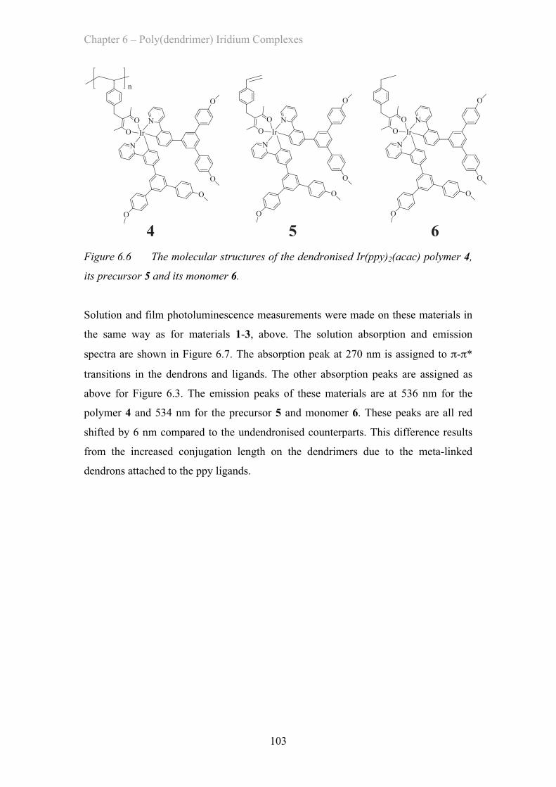
Chapter 6 – Poly(dendrimer) Iridium Complexes
103
4 5 6
Figure 6.6 The molecular structures of the dendronised Ir(ppy)2(acac) polymer 4,
its precursor 5 and its monomer 6.
Solution and film photoluminescence measurements were made on these materials in
the same way as for materials 1-3, above. The solution absorption and emission
spectra are shown in Figure 6.7. The absorption peak at 270 nm is assigned to π-π*
transitions in the dendrons and ligands. The other absorption peaks are assigned as
above for Figure 6.3. The emission peaks of these materials are at 536 nm for the
polymer 4 and 534 nm for the precursor 5 and monomer 6. These peaks are all red
shifted by 6 nm compared to the undendronised counterparts. This difference results
from the increased conjugation length on the dendrimers due to the meta-linked
dendrons attached to the ppy ligands.
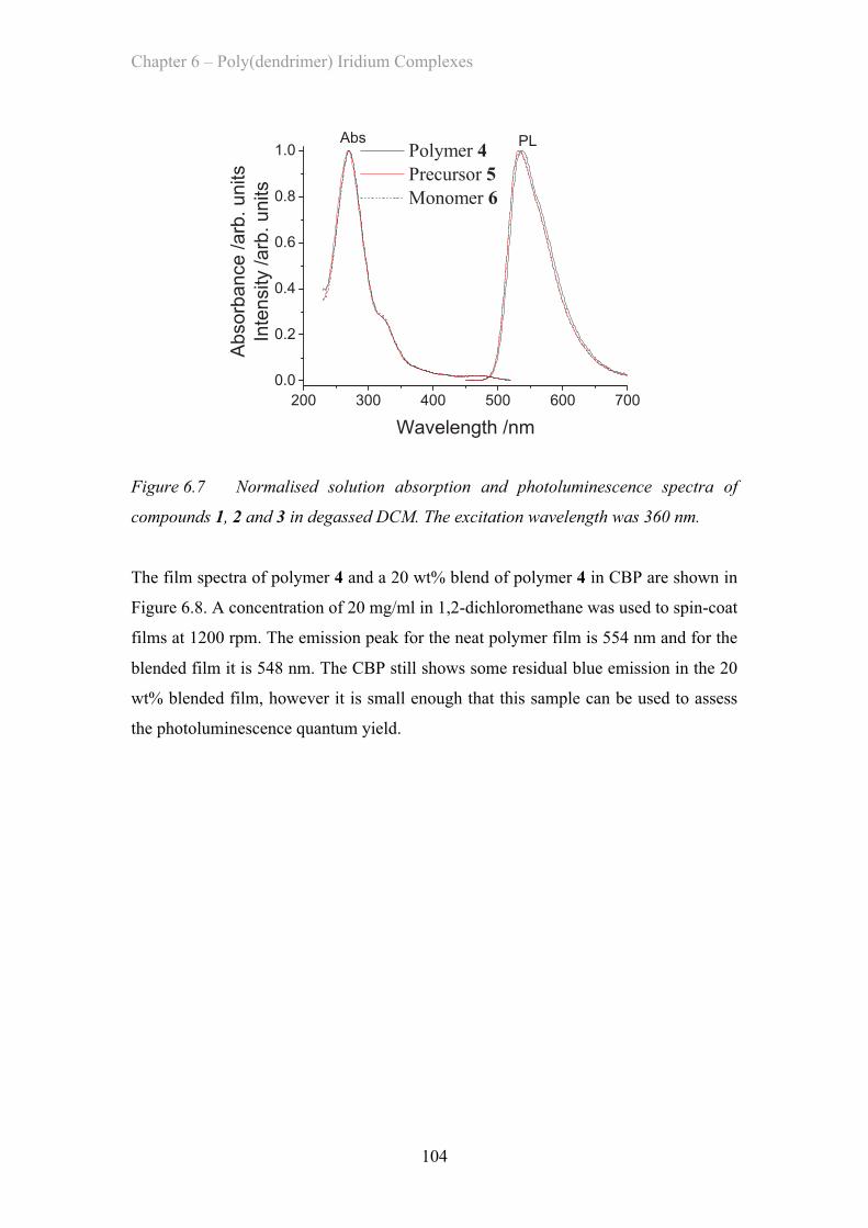
Chapter 6 – Poly(dendrimer) Iridium Complexes
104
Figure 6.7 Normalised solution absorption and photoluminescence spectra of
compounds 1, 2 and 3 in degassed DCM. The excitation wavelength was 360 nm.
The film spectra of polymer 4 and a 20 wt% blend of polymer 4 in CBP are shown in
Figure 6.8. A concentration of 20 mg/ml in 1,2-dichloromethane was used to spin-coat
films at 1200 rpm. The emission peak for the neat polymer film is 554 nm and for the
blended film it is 548 nm. The CBP still shows some residual blue emission in the 20
wt% blended film, however it is small enough that this sample can be used to assess
the photoluminescence quantum yield.
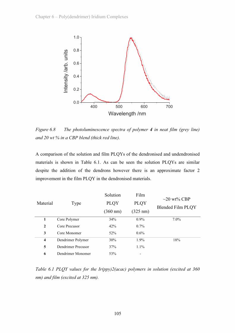
Chapter 6 – Poly(dendrimer) Iridium Complexes
105
400 500 600 7000.0
0.2
0.4
0.6
0.8
1.0
Inte
nsity
/arb
. units
Wavelength /nm
Figure 6.8 The photoluminescence spectra of polymer 4 in neat film (grey line)
and 20 wt % in a CBP blend (thick red line).
A comparison of the solution and film PLQYs of the dendronised and undendronised
materials is shown in Table 6.1. As can be seen the solution PLQYs are similar
despite the addition of the dendrons however there is an approximate factor 2
improvement in the film PLQY in the dendronised materials.
Material Type
Solution
PLQY
(360 nm)
Film
PLQY
(325 nm)
~20 wt% CBP
Blended Film PLQY
1 Core Polymer 34% 0.9% 7.0%
2 Core Precusor 42% 0.7%
3 Core Monomer 52% 0.6%
4 Dendrimer Polymer 30% 1.9% 18%
5 Dendrimer Precusor 37% 1.1%
6 Dendrimer Monomer 53% -
Table 6.1 PLQY values for the Ir(ppy)2(acac) polymers in solution (excited at 360
nm) and film (excited at 325 nm).
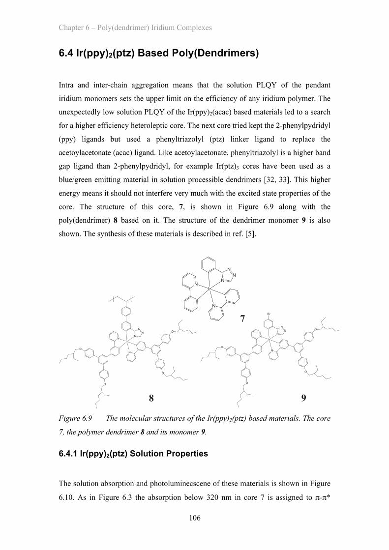
Chapter 6 – Poly(dendrimer) Iridium Complexes
106
6.4 Ir(ppy)2(ptz) Based Poly(Dendrimers)
Intra and inter-chain aggregation means that the solution PLQY of the pendant
iridium monomers sets the upper limit on the efficiency of any iridium polymer. The
unexpectedly low solution PLQY of the Ir(ppy)2(acac) based materials led to a search
for a higher efficiency heteroleptic core. The next core tried kept the 2-phenylpydridyl
(ppy) ligands but used a phenyltriazolyl (ptz) linker ligand to replace the
acetoylacetonate (acac) ligand. Like acetoylacetonate, phenyltriazolyl is a higher band
gap ligand than 2-phenylpydridyl, for example Ir(ptz)3 cores have been used as a
blue/green emitting material in solution processible dendrimers [32, 33]. This higher
energy means it should not interfere very much with the excited state properties of the
core. The structure of this core, 7, is shown in Figure 6.9 along with the
poly(dendrimer) 8 based on it. The structure of the dendrimer monomer 9 is also
shown. The synthesis of these materials is described in ref. [5].
7
8 9
Figure 6.9 The molecular structures of the Ir(ppy)2(ptz) based materials. The core
7, the polymer dendrimer 8 and its monomer 9.
6.4.1 Ir(ppy)2(ptz) Solution Properties
The solution absorption and photoluminecscene of these materials is shown in Figure
6.10. As in Figure 6.3 the absorption below 320 nm in core 7 is assigned to π-π*
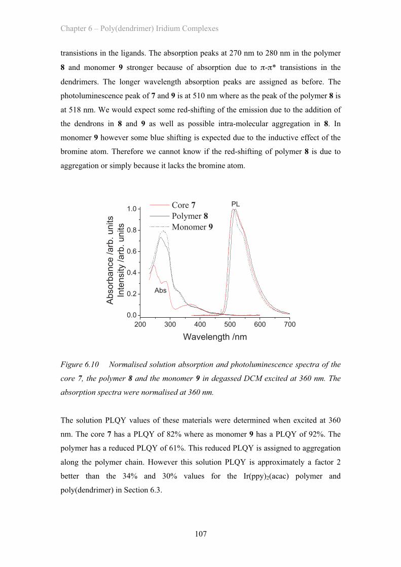
Chapter 6 – Poly(dendrimer) Iridium Complexes
107
transistions in the ligands. The absorption peaks at 270 nm to 280 nm in the polymer
8 and monomer 9 stronger because of absorption due to π-π* transistions in the
dendrimers. The longer wavelength absorption peaks are assigned as before. The
photoluminescence peak of 7 and 9 is at 510 nm where as the peak of the polymer 8 is
at 518 nm. We would expect some red-shifting of the emission due to the addition of
the dendrons in 8 and 9 as well as possible intra-molecular aggregation in 8. In
monomer 9 however some blue shifting is expected due to the inductive effect of the
bromine atom. Therefore we cannot know if the red-shifting of polymer 8 is due to
aggregation or simply because it lacks the bromine atom.
Figure 6.10 Normalised solution absorption and photoluminescence spectra of the
core 7, the polymer 8 and the monomer 9 in degassed DCM excited at 360 nm. The
absorption spectra were normalised at 360 nm.
The solution PLQY values of these materials were determined when excited at 360
nm. The core 7 has a PLQY of 82% where as monomer 9 has a PLQY of 92%. The
polymer has a reduced PLQY of 61%. This reduced PLQY is assigned to aggregation
along the polymer chain. However this solution PLQY is approximately a factor 2
better than the 34% and 30% values for the Ir(ppy)2(acac) polymer and
poly(dendrimer) in Section 6.3.
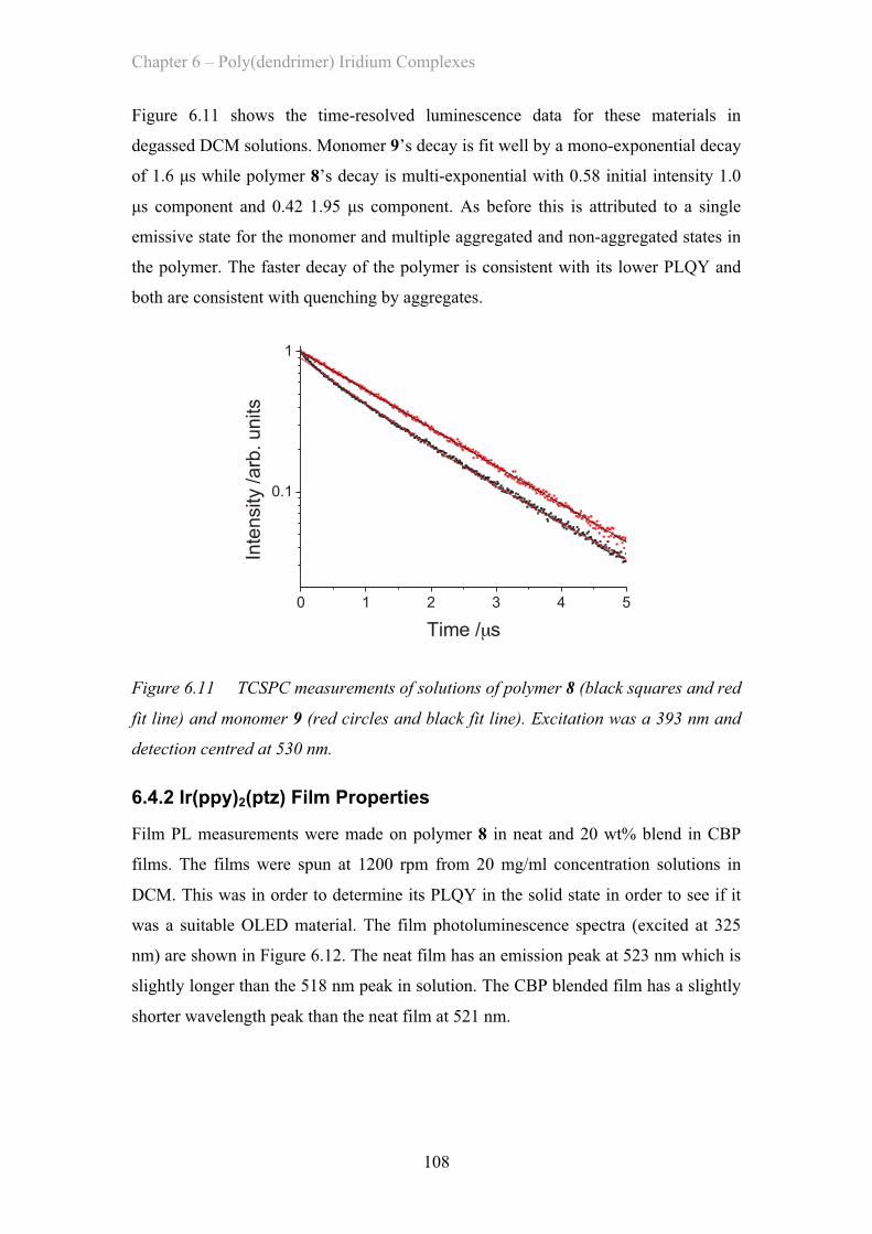
Chapter 6 – Poly(dendrimer) Iridium Complexes
108
Figure 6.11 shows the time-resolved luminescence data for these materials in
degassed DCM solutions. Monomer 9’s decay is fit well by a mono-exponential decay
of 1.6 µs while polymer 8’s decay is multi-exponential with 0.58 initial intensity 1.0
µs component and 0.42 1.95 µs component. As before this is attributed to a single
emissive state for the monomer and multiple aggregated and non-aggregated states in
the polymer. The faster decay of the polymer is consistent with its lower PLQY and
both are consistent with quenching by aggregates.
0 1 2 3 4 5
0.1
1
Inte
nsity /arb
. units
Time /µs
Figure 6.11 TCSPC measurements of solutions of polymer 8 (black squares and red
fit line) and monomer 9 (red circles and black fit line). Excitation was a 393 nm and
detection centred at 530 nm.
6.4.2 Ir(ppy)2(ptz) Film Properties
Film PL measurements were made on polymer 8 in neat and 20 wt% blend in CBP
films. The films were spun at 1200 rpm from 20 mg/ml concentration solutions in
DCM. This was in order to determine its PLQY in the solid state in order to see if it
was a suitable OLED material. The film photoluminescence spectra (excited at 325
nm) are shown in Figure 6.12. The neat film has an emission peak at 523 nm which is
slightly longer than the 518 nm peak in solution. The CBP blended film has a slightly
shorter wavelength peak than the neat film at 521 nm.
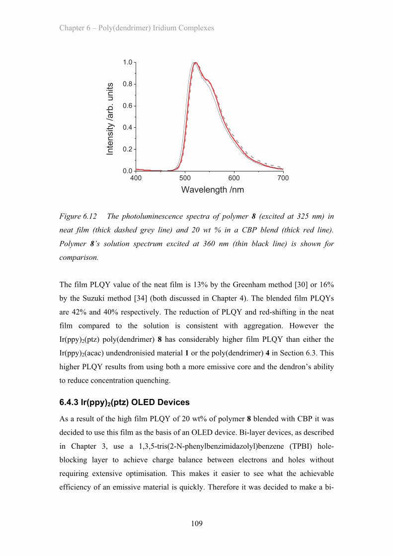
Chapter 6 – Poly(dendrimer) Iridium Complexes
109
400 500 600 7000.0
0.2
0.4
0.6
0.8
1.0
Inte
nsity
/arb
. units
Wavelength /nm
Figure 6.12 The photoluminescence spectra of polymer 8 (excited at 325 nm) in
neat film (thick dashed grey line) and 20 wt % in a CBP blend (thick red line).
Polymer 8’s solution spectrum excited at 360 nm (thin black line) is shown for
comparison.
The film PLQY value of the neat film is 13% by the Greenham method [30] or 16%
by the Suzuki method [34] (both discussed in Chapter 4). The blended film PLQYs
are 42% and 40% respectively. The reduction of PLQY and red-shifting in the neat
film compared to the solution is consistent with aggregation. However the
Ir(ppy)2(ptz) poly(dendrimer) 8 has considerably higher film PLQY than either the
Ir(ppy)2(acac) undendronisied material 1 or the poly(dendrimer) 4 in Section 6.3. This
higher PLQY results from using both a more emissive core and the dendron’s ability
to reduce concentration quenching.
6.4.3 Ir(ppy)2(ptz) OLED Devices
As a result of the high film PLQY of 20 wt% of polymer 8 blended with CBP it was
decided to use this film as the basis of an OLED device. Bi-layer devices, as described
in Chapter 3, use a 1,3,5-tris(2-N-phenylbenzimidazolyl)benzene (TPBI) hole-
blocking layer to achieve charge balance between electrons and holes without
requiring extensive optimisation. This makes it easier to see what the achievable
efficiency of an emissive material is quickly. Therefore it was decided to make a bi-
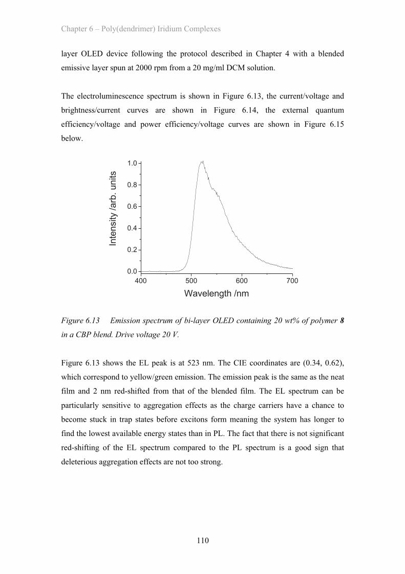
Chapter 6 – Poly(dendrimer) Iridium Complexes
110
layer OLED device following the protocol described in Chapter 4 with a blended
emissive layer spun at 2000 rpm from a 20 mg/ml DCM solution.
The electroluminescence spectrum is shown in Figure 6.13, the current/voltage and
brightness/current curves are shown in Figure 6.14, the external quantum
efficiency/voltage and power efficiency/voltage curves are shown in Figure 6.15
below.
400 500 600 700
0.0
0.2
0.4
0.6
0.8
1.0
Inte
nsity /arb
. units
Wavelength /nm
Figure 6.13 Emission spectrum of bi-layer OLED containing 20 wt% of polymer 8
in a CBP blend. Drive voltage 20 V.
Figure 6.13 shows the EL peak is at 523 nm. The CIE coordinates are (0.34, 0.62),
which correspond to yellow/green emission. The emission peak is the same as the neat
film and 2 nm red-shifted from that of the blended film. The EL spectrum can be
particularly sensitive to aggregation effects as the charge carriers have a chance to
become stuck in trap states before excitons form meaning the system has longer to
find the lowest available energy states than in PL. The fact that there is not significant
red-shifting of the EL spectrum compared to the PL spectrum is a good sign that
deleterious aggregation effects are not too strong.
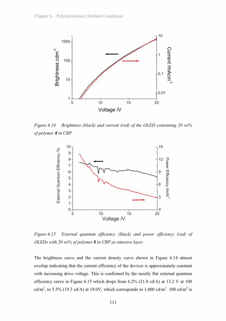
Chapter 6 – Poly(dendrimer) Iridium Complexes
111
5 10 15 201
10
100
1000
0.01
0.1
1
10
Curre
nt /m
Acm
-2B
rightn
ess c
dm
-2
Voltage /V
Figure 6.14 Brightness (black) and current (red) of the OLED containing 20 wt%
of polymer 8 in CBP.
5 10 15 200
1
2
3
4
5
6
7
8
9
10
0
3
6
9
12
15
Po
we
r Effic
ien
cy /lm
W-1
Exte
rna
l Q
ua
ntu
m E
ffic
ien
cy /
%
Voltage /V
Figure 6.15 External quantum efficiency (black) and power efficiency (red) of
OLEDs with 20 wt% of polymer 8 in CBP as emissive layer.
The brightness curve and the current density curve shown in Figure 6.14 almost
overlap indicating that the current efficiency of the devices is approximately constant
with increasing drive voltage. This is confirmed by the mostly flat external quantum
efficiency curve in Figure 6.15 which drops from 6.2% (21.8 cd/A) at 13.2 V at 100
cd/m2, to 5.5% (19.3 cd/A) at 19.0V, which corresponds to 1,000 cd/m2. 100 cd/m2 is
Chapter 6 – Poly(dendrimer) Iridium Complexes
112
normally taken as the benchmark brightness for a display application. Unfortunately
the drive voltage of 13.2 V for this brightness and the turn on voltage (brightness 1
cd/m2) of 6.2 V are a little too high for device applications and negatively impact the
power efficiency. These values could be reduced by reduction and optimisation of the
layer thicknesses and improved charge injection at the cathode for applications in
actual devices.
The external quantum efficiency of 6.2% is ~80% of the theoretical maximum
efficiency of 8% arrived at by assuming 20% out-coupling efficiency, perfect charge
recombination and using the 40% PLQY value of the blended film. This suggests that
the bi-layer structure has done a good job of balancing the electron and hole currents
but that some further optimisation is possible.
6.5 Doubly Dendronised Ir(ppy)2(ptz) Polymer The dendrimer concept uses the dendrimer arms to protect the emissive core from
aggregating with its neighbours via steric interactions. Nevertheless the most efficient
dendrimer OLEDs still make use of a charge transporting host like CBP or 4,4’,4’’-
tris(N-carbazoyl)triphenylamine (TCTA) to increase the film PLQY and device
efficiency by helping to separate the cores [3]. These blended devices achieved 16%
EQE. Another solution that has been used is to add a second set of dendrons to each
ligand, thereby better encapsulating each core and protecting it from its neighbours
[35]. This has allowed 13.6% EQE to be achieved in neat film devices.
As the Ir(ppy)2(ptz) poly(dendimer) in Section 6.4 was already achieving close to its
theoretical maximum OLED efficiency it was decided to try and improve the film
luminescence quantum yields and thus the device efficiencies of the poly(dendrimers)
by adopting a double-dendron structure. The structures of the polymer and its
corresponding polymer are shown as materials 10 and 11 in Figure 6.16 below.
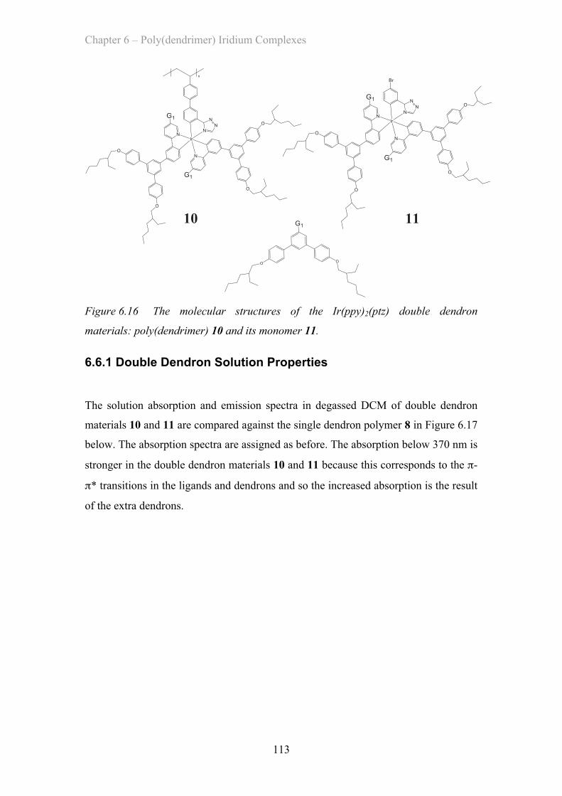
Chapter 6 – Poly(dendrimer) Iridium Complexes
113
10 11
Figure 6.16 The molecular structures of the Ir(ppy)2(ptz) double dendron
materials: poly(dendrimer) 10 and its monomer 11.
6.6.1 Double Dendron Solution Properties
The solution absorption and emission spectra in degassed DCM of double dendron
materials 10 and 11 are compared against the single dendron polymer 8 in Figure 6.17
below. The absorption spectra are assigned as before. The absorption below 370 nm is
stronger in the double dendron materials 10 and 11 because this corresponds to the π-
π* transitions in the ligands and dendrons and so the increased absorption is the result
of the extra dendrons.
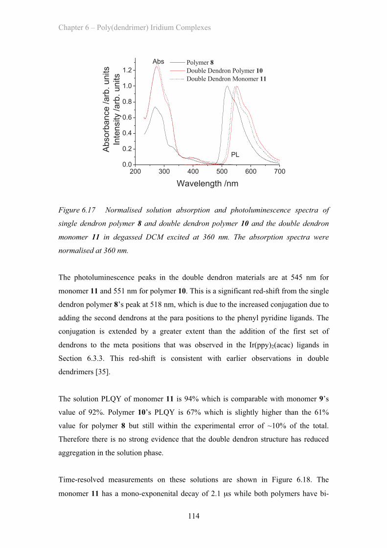
Chapter 6 – Poly(dendrimer) Iridium Complexes
114
Figure 6.17 Normalised solution absorption and photoluminescence spectra of
single dendron polymer 8 and double dendron polymer 10 and the double dendron
monomer 11 in degassed DCM excited at 360 nm. The absorption spectra were
normalised at 360 nm.
The photoluminescence peaks in the double dendron materials are at 545 nm for
monomer 11 and 551 nm for polymer 10. This is a significant red-shift from the single
dendron polymer 8’s peak at 518 nm, which is due to the increased conjugation due to
adding the second dendrons at the para positions to the phenyl pyridine ligands. The
conjugation is extended by a greater extent than the addition of the first set of
dendrons to the meta positions that was observed in the Ir(ppy)2(acac) ligands in
Section 6.3.3. This red-shift is consistent with earlier observations in double
dendrimers [35].
The solution PLQY of monomer 11 is 94% which is comparable with monomer 9’s
value of 92%. Polymer 10’s PLQY is 67% which is slightly higher than the 61%
value for polymer 8 but still within the experimental error of ~10% of the total.
Therefore there is no strong evidence that the double dendron structure has reduced
aggregation in the solution phase.
Time-resolved measurements on these solutions are shown in Figure 6.18. The
monomer 11 has a mono-exponenital decay of 2.1 µs while both polymers have bi-
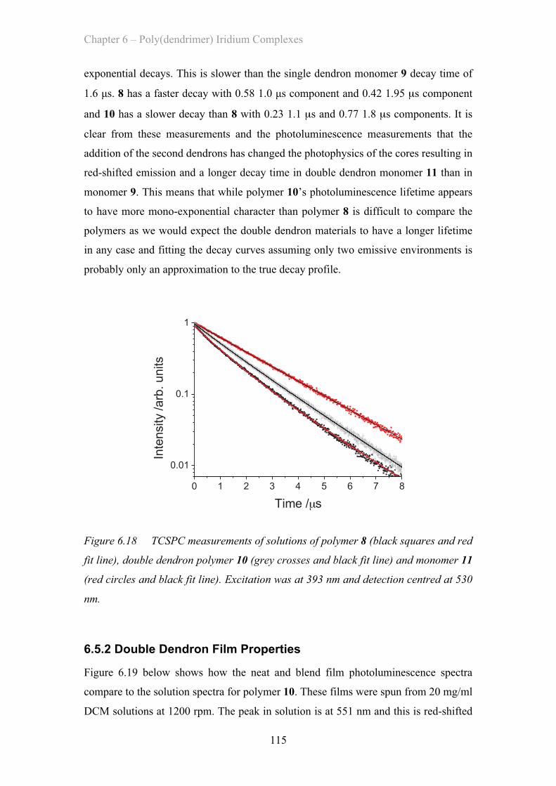
Chapter 6 – Poly(dendrimer) Iridium Complexes
115
exponential decays. This is slower than the single dendron monomer 9 decay time of
1.6 µs. 8 has a faster decay with 0.58 1.0 µs component and 0.42 1.95 µs component
and 10 has a slower decay than 8 with 0.23 1.1 µs and 0.77 1.8 µs components. It is
clear from these measurements and the photoluminescence measurements that the
addition of the second dendrons has changed the photophysics of the cores resulting in
red-shifted emission and a longer decay time in double dendron monomer 11 than in
monomer 9. This means that while polymer 10’s photoluminescence lifetime appears
to have more mono-exponential character than polymer 8 is difficult to compare the
polymers as we would expect the double dendron materials to have a longer lifetime
in any case and fitting the decay curves assuming only two emissive environments is
probably only an approximation to the true decay profile.
0 1 2 3 4 5 6 7 8
0.01
0.1
1
Inte
nsity
/arb
. units
Time /µs
Figure 6.18 TCSPC measurements of solutions of polymer 8 (black squares and red
fit line), double dendron polymer 10 (grey crosses and black fit line) and monomer 11
(red circles and black fit line). Excitation was at 393 nm and detection centred at 530
nm.
6.5.2 Double Dendron Film Properties
Figure 6.19 below shows how the neat and blend film photoluminescence spectra
compare to the solution spectra for polymer 10. These films were spun from 20 mg/ml
DCM solutions at 1200 rpm. The peak in solution is at 551 nm and this is red-shifted
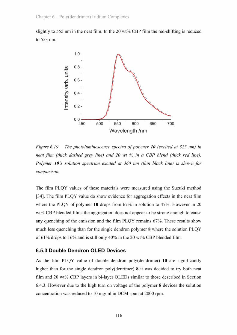
Chapter 6 – Poly(dendrimer) Iridium Complexes
116
slightly to 555 nm in the neat film. In the 20 wt% CBP film the red-shifting is reduced
to 553 nm.
450 500 550 600 650 7000.0
0.2
0.4
0.6
0.8
1.0
Inte
nsity
/arb
. units
Wavelength /nm
Figure 6.19 The photoluminescence spectra of polymer 10 (excited at 325 nm) in
neat film (thick dashed grey line) and 20 wt % in a CBP blend (thick red line).
Polymer 10’s solution spectrum excited at 360 nm (thin black line) is shown for
comparison.
The film PLQY values of these materials were measured using the Suzuki method
[34]. The film PLQY value do show evidence for aggregation effects in the neat film
where the PLQY of polymer 10 drops from 67% in solution to 47%. However in 20
wt% CBP blended films the aggregation does not appear to be strong enough to cause
any quenching of the emission and the film PLQY remains 67%. These results show
much less quenching than for the single dendron polymer 8 where the solution PLQY
of 61% drops to 16% and is still only 40% in the 20 wt% CBP blended film.
6.5.3 Double Dendron OLED Devices
As the film PLQY value of double dendron poly(dendrimer) 10 are significantly
higher than for the single dendron poly(denrimer) 8 it was decided to try both neat
film and 20 wt% CBP layers in bi-layer OLEDs similar to those described in Section
6.4.3. However due to the high turn on voltage of the polymer 8 devices the solution
concentration was reduced to 10 mg/ml in DCM spun at 2000 rpm.
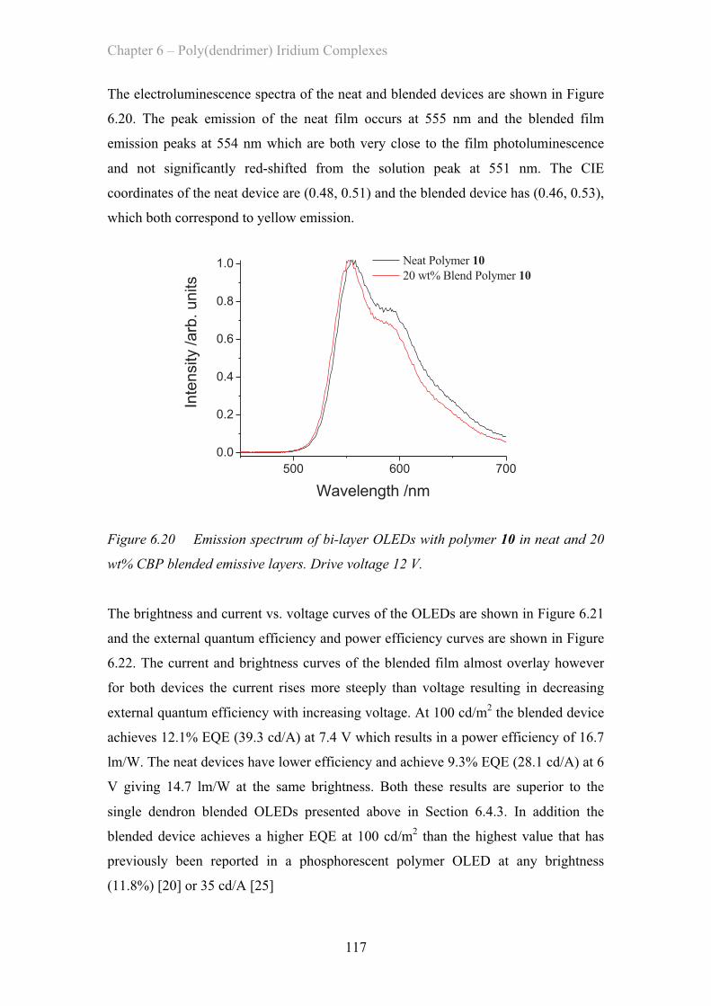
Chapter 6 – Poly(dendrimer) Iridium Complexes
117
The electroluminescence spectra of the neat and blended devices are shown in Figure
6.20. The peak emission of the neat film occurs at 555 nm and the blended film
emission peaks at 554 nm which are both very close to the film photoluminescence
and not significantly red-shifted from the solution peak at 551 nm. The CIE
coordinates of the neat device are (0.48, 0.51) and the blended device has (0.46, 0.53),
which both correspond to yellow emission.
500 600 700
0.0
0.2
0.4
0.6
0.8
1.0 Neat Polymer 10 20 wt% Blend Polymer 10
Inte
nsity /arb
. units
Wavelength /nm
Figure 6.20 Emission spectrum of bi-layer OLEDs with polymer 10 in neat and 20
wt% CBP blended emissive layers. Drive voltage 12 V.
The brightness and current vs. voltage curves of the OLEDs are shown in Figure 6.21
and the external quantum efficiency and power efficiency curves are shown in Figure
6.22. The current and brightness curves of the blended film almost overlay however
for both devices the current rises more steeply than voltage resulting in decreasing
external quantum efficiency with increasing voltage. At 100 cd/m2 the blended device
achieves 12.1% EQE (39.3 cd/A) at 7.4 V which results in a power efficiency of 16.7
lm/W. The neat devices have lower efficiency and achieve 9.3% EQE (28.1 cd/A) at 6
V giving 14.7 lm/W at the same brightness. Both these results are superior to the
single dendron blended OLEDs presented above in Section 6.4.3. In addition the
blended device achieves a higher EQE at 100 cd/m2 than the highest value that has
previously been reported in a phosphorescent polymer OLED at any brightness
(11.8%) [20] or 35 cd/A [25]
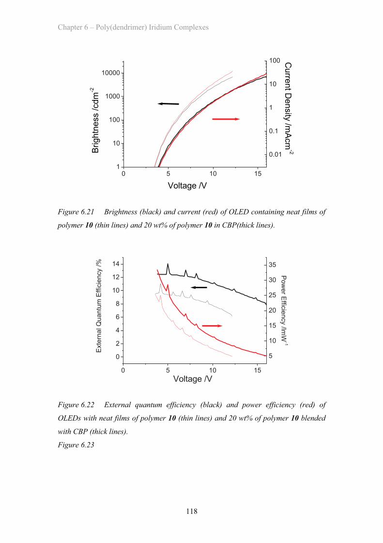
Chapter 6 – Poly(dendrimer) Iridium Complexes
118
0 5 10 151
10
100
1000
10000
0.01
0.1
1
10
100 Curre
nt D
ensity
/mA
cm
-2Brightn
ess /cdm
-2
Voltage /V
Figure 6.21 Brightness (black) and current (red) of OLED containing neat films of
polymer 10 (thin lines) and 20 wt% of polymer 10 in CBP(thick lines).
0 5 10 15
0
2
4
6
8
10
12
14
5
10
15
20
25
30
35
Po
we
r Effic
ien
cy /lm
W-1
Exte
rna
l Q
ua
ntu
m E
ffic
ien
cy /
%
Voltage /V
Figure 6.22 External quantum efficiency (black) and power efficiency (red) of
OLEDs with neat films of polymer 10 (thin lines) and 20 wt% of polymer 10 blended
with CBP (thick lines).
Figure 6.23
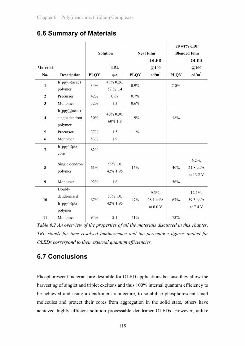
Chapter 6 – Poly(dendrimer) Iridium Complexes
119
6.6 Summary of Materials
Material
No. Description
Solution Neat Film
20 wt% CBP
Blended Film
PLQY
TRL
/µµs PLQY
OLED
@100
cd/m2 PLQY
OLED
@100
cd/m2
1 Ir(ppy)2(acac)
polymer 34%
48% 0.26,
52 % 1.4 0.9% 7.0%
2 Precursor 42% 0.67 0.7%
3 Monomer 52% 1.3 0.6%
4
Ir(ppy)2(acac)
single dendron
polymer
30% 40% 0.30,
60% 1.8 1.9% 18%
5 Precursor 37% 1.5 1.1%
6 Monomer 53% 1.9
7 Ir(ppy)2(ptz)
core 82%
8 Single dendron
polymer 61%
58% 1.0,
42% 1.95 16% 40%
6.2%,
21.8 cd/A
at 13.2 V
9 Monomer 92% 1.6 56%
10
Doubly
dendronised
Ir(ppy)2(ptz)
polymer
67% 58% 1.0,
42% 1.95 47%
9.3%,
28.1 cd/A
at 6.0 V
67%
12.1%,
39.3 cd/A
at 7.4 V
11 Monomer 94% 2.1 41% 73%
Table 6.2 An overview of the properties of all the materials discussed in this chapter.
TRL stands for time resolved luminescence and the percentage figures quoted for
OLEDs correspond to their external quantum efficiencies.
6.7 Conclusions
Phosphorescent materials are desirable for OLED applications because they allow the
harvesting of singlet and triplet excitons and thus 100% internal quantum efficiency to
be achieved and using a dendrimer architecture, to solubilise phosphorescent small
molecules and protect their cores from aggregation in the solid state, others have
achieved highly efficient solution processable dendrimer OLEDs. However, unlike

Chapter 6 – Poly(dendrimer) Iridium Complexes
120
fluorescent polymers, these molecules do not give their solutions the viscosity
necessary for ink-jet printing. This requires us to develop phosphorescent polymers
that can be used to produce highly efficient ink-jet printable devices.
Using a non-conjugated polymer backbone to prevent quenching of the
phosphorescence, the properties of these materials have been explored over the course
of this chapter. The materials have been developed starting with a Ir(ppy)2(acac) core
and no dendrons. The resulting polymer was found to produce high enough viscosity
solutions to allow inkjet printing [29]. It was then demonstrated that adding dendrons
to the core reduced aggregation quenching in the solid state resulting in a factor 2
increase in solid state performance. Unfortunately these materials still suffered from
low photoluminescence quantum yields and unexpectedly long wavelength emission,
possibly due to problems with the acac ligand.
By switching to a Ir(ppy)2(ptz) core the solution photoluminescence quantum yield
was increased by a factor of 2 while retaining the required viscosity for inkjet printing
[5]. The dendrimer structure allowed a blended film quantum yield of 40% which was
high enough to allow OLED devices with 6.2% EQE at 100 cd/m2 to be made. The
aggregation in the solid state was further reduced by adding extra dendrons to make
double dendron materials and, while these showed only a modest improvement in
solution they had, greatly improved film PLQY to 67%. As film PLQY is a very
important parameter for OLED devices this resulted in greatly improved OLEDs with
12.1% EQE (39.3 cd/A) at 100 cd/m2. These doubly dendronised polymer OLEDs
showed a higher efficiency than the 11.8% EQE [20] or 35.1 cd/A [25] of the best
previously reported phosphorescent polymer devices.
Throughout this chapter the solution quantum yield of the monomer materials has
been higher than the polymers and the time-resolved luminescence data has showed
the polymers contain multiple emissive environments. This is because the polymers
have closely spaced pendant iridium complexes that can concentration quench. This
intrachain aggregation does not seem to be significantly affected by using no-
dendrons, single dendrons or double dendrons and so an alternative strategy, of
separating the iridium cores on the polymers using spacer groups and creating a co-
polymer, will be discussed in the next chapter.
Chapter 6 – Poly(dendrimer) Iridium Complexes
121
1. King, K.A., P.J. Spellane, and R.J. Watts, Excited-State Properties of a Triply Ortho-Metalated Iridium(III) Complex. Journal of the American Chemical Society, 1985. 107(5): p. 1431-1432.
2. Baldo, M.A., et al., Very high-efficiency green organic light-emitting devices based on electrophosphorescence. Applied Physics Letters, 1999. 75(1): p. 4-6.
3. Lo, S.C., et al., Green phosphorescent dendrimer for light-emitting diodes. Advanced Materials, 2002. 14(13-14): p. 975.
4. Gunning, J.P., et al., The development of poly(dendrimer)s for advanced processing. Polymer Chemistry, 2010. 1(5): p. 730-738.
5. Lai, W.Y., et al., A Phosphorescent Poly(dendrimer) Containing Iridium(III) Complexes: Synthesis and Light-Emitting Properties. Macromolecules, 2010. 43(17): p. 6986-6994.
6. Tekin, E., et al., Ink-jet printing of luminescent ruthenium- and iridium-containing polymers for applications in light-emitting devices. Macromolecular Rapid Communications, 2005. 26(4): p. 293-297.
7. Singh, M., et al., Inkjet Printing-Process and Its Applications. Advanced Materials, 2010. 22(6): p. 673-685.
8. Shimoda, T., et al., Inkjet printing of light-emitting polymer displays. Mrs Bulletin, 2003. 28(11): p. 821-827.
9. Sandee, A.J., et al., Solution-processible conjugated electrophosphorescent polymers. Journal of the American Chemical Society, 2004. 126(22): p. 7041-7048.
10. Evans, N.R., et al., Triplet energy back transfer in conjugated polymers with pendant phosphorescent iridium complexes. Journal of the American Chemical Society, 2006. 128(20): p. 6647-6656.
11. Zhen, H.Y., et al., Electrophosphorescent chelating copolymers based on linkage isomers of naphthylpyridine-iridium complexes with fluorene. Macromolecules, 2006. 39(5): p. 1693-1700.
12. Jiang, J.X., et al., High-efficiency electrophosphorescent fluorene-alt-carbazole copolymers N-grafted with cyclometalated Ir complexes. Macromolecules, 2005. 38(10): p. 4072-4080.
13. Chen, X.W., et al., High-efficiency red-light emission from polyfluorenes grafted with cyclometalated iridium complexes and charge transport moiety. Journal of the American Chemical Society, 2003. 125(3): p. 636-637.
14. Sudhakar, M., et al., Phosphorescence quenching by conjugated polymers. Journal of the American Chemical Society, 2003. 125(26): p. 7796-7797.
15. Schulz, G.L., et al., Enhancement of phosphorescence of Ir complexes bound to conjugated polymers: Increasing the triplet level of the main chain. Macromolecules, 2006. 39(26): p. 9157-9165.
16. Yang, W., et al., Synthesis of electrophosphorescent polymers based on para-phenylenes with iridium complexes. Synthetic Metals, 2005. 153(1-3): p. 189-192.
17. Vicente, J., et al., Synthesis and Luminescence of Poly(phenylacetylene)s with Pendant Iridium Complexes and Carbazole Groups. Journal of Polymer Science Part a-Polymer Chemistry, 2010. 48(17): p. 3744-3757.
18. Tokito, S., M. Suzuki, and F. Sato, Improvement of emission efficiency in polymer light-emitting devices based on phosphorescent polymers. Thin Solid Films, 2003. 445: p. 353–357.
Chapter 6 – Poly(dendrimer) Iridium Complexes
122
19. Tokito, S., et al., High-efficiency phosphorescent polymer light-emitting devices. Organic Electronics, 2003. 4: p. 105–111.
20. Suzuki, M., et al., Highly efficient polymer light-emitting devices using ambipolar phosphorescent polymers. Applied Physics Letters, 2005. 86(10): p. 103507.
21. Deng, L., et al., Living radical polymerization of bipolar transport materials for highly efficient light emitting diodes. Chemistry of Materials, 2006. 18(2): p. 386-395.
22. Furuta, P.T., et al., Platinum-functionalized random copolymers for use in solution-processible, efficient, near-white organic light-emitting diodes. Journal of the American Chemical Society, 2004. 126(47): p. 15388-15389.
23. Wang, X.Y., et al., Polymer-based tris(2-phenylpyridine)iridium complexes. Macromolecules, 2006. 39(9): p. 3140-3146.
24. Wang, X.Y., A. Kimyonok, and M. Weck, Functionalization of polymers with phosphorescent iridium complexes via click chemistry. Chemical Communications, 2006(37): p. 3933-3935.
25. Thesen, M.W., et al., Hole-Transporting Host-Polymer Series Consisting of Triphenylamine Basic Structures for Phosphorescent Polymer Light-Emitting Diodes. Journal of Polymer Science Part a-Polymer Chemistry, 2010. 48(15): p. 3417-3430.
26. Thesen, M.W., et al., Investigation of Spacer Influences in Phosphorescent-Emitting Nonconjugated PLED Systems. Journal of Polymer Science Part a-Polymer Chemistry, 2010. 48(2): p. 389-402.
27. Adachi, C., et al., Nearly 100% internal phosphorescence efficiency in an organic light-emitting device. Journal of Applied Physics, 2001. 90(10): p. 5048-5051.
28. Hay, P.J., Theoretical studies of the ground and excited electronic states in cyclometalated phenylpyridine Ir(III) complexes using density functional theory. Journal of Physical Chemistry A, 2002. 106(8): p. 1634-1641.
29. Lai, W.Y., et al., A study on the preparation and photophysical properties of an iridium(III) complexed homopolymer. Journal of Materials Chemistry, 2009. 19(28): p. 4952-4959.
30. Greenham, N.C., et al., Measurement of Absolute Photoluminescence Quantum Efficiencies in Conjugated Polymers. Chemical Physics Letters, 1995. 241(1-2): p. 89-96.
31. Namdas, E.B., et al., Photophysics of Fac-tris(2-phenylpyridine) iridium(III) cored electroluminescent dendrimers in solution and films. Journal of Physical Chemistry B, 2004. 108(5): p. 1570-1577.
32. Lo, S.C., et al., Blue phosphorescence from iridium(III) complexes at room temperature. Chemistry of Materials, 2006. 18(21): p. 5119-5129.
33. Lo, S.C., et al., Solution-Processible Phosphorescent Blue Dendrimers Based on Biphenyl-Dendrons and Fac-tris(phenyltriazolyl)iridium(III) Cores. Advanced Functional Materials, 2008. 18(19): p. 3080-3090.
34. Suzuki, K., et al., Reevaluation of absolute luminescence quantum yields of standard solutions using a spectrometer with an integrating sphere and a back-thinned CCD detector. Physical Chemistry Chemical Physics, 2009. 11(42): p. 9850-9860.
35. Lo, S.C., et al., Encapsulated cores: Host-free organic light-emitting diodes based on solution-processible electrophosphorescent dendrimers. Advanced Materials, 2005. 17(16): p. 1945-+.
123
7. Phosphorescent Copolymer Dendrimers
7.1 Introduction .......................................................................................................... 123�7.2 Poly(styrene) copolymers .................................................................................... 124�
7.2.1 Solution Properties - Poly(styrene) co-polymer ....................................... 125�7.2.2 Film Properties - Poly(styrene) co-polymer ............................................. 127�7.2.3 OLED Device Properties - Poly(styrene) co-polymer .............................. 128�
7.3 Poly(carbazole) copolymers ................................................................................. 131�7.3.1 Solution Properties - Poly(carbazole) co-polymers .................................. 132�7.3.2 Film Properties - Poly(carbazole) co-polymers ........................................ 137�7.3.3 Neat OLED Device Properties - Poly(carbazole) co-polymers ................ 139�7.3.4 Blended Film Properties - Poly(carbazole) co-polymers .......................... 141�7.3.5 Blended OLED Device Properties - Poly(carbazole) co-polymers .......... 143�
7.4 Summary of Materials .......................................................................................... 146�7.5 Conclusions .......................................................................................................... 146�
7.1 Introduction
In this chapter I will discuss a continuation to the work on phosphorescent polymers
for ink jet printable OLEDs that was started in Chapter 6. In this chapter a copolymer
approach was used to control intra-chain aggregation that was observed in the homo-
polymers in Chapter 6, which reduced their efficiency as light emitters. These
interactions manifested themselves as decreases in photoluminescence efficiency of
the polymers compared to their monomers and multiple lifetime components
appearing in time resolved luminescence measurements.
In order to reduce these interactions higher energy spacer units are inserted between
the phosphorescent cores. The higher band gap energy of these spacers means they
should not suffer from back transfer of triplet states from the iridium complexes [1, 2]
and any excited states formed on the spacer units will be transferred to the emissive
cores. Previous work on iridium based phosphorescent copolymers has been done by
Chapter 7 – Phosphorescent Copolymer Dendrimers
124
others [1, 3-11] however these authors only made use of pendant iridum complexes
which were susceptible to aggregation, limiting device efficiency.
As many of the materials in this chapter are related to those in the previous chapter on
phosphorescent polymers the material numbers will continue on from those in the
previous chapter. Once again the materials were made and chemically characterised
by Wen-Yong Lai, Shih-Chun Lo and Paul Burn at the University of Queensland. The
spacer unit that was used initially was poly(styrene) and single dendron copolymers
use it as a spacer unit are discussed in Section 7.2, including solution, film and OLED
device results. As poly(styrene)’s high HOMO-LUMO gap required additional charge
transporting CBP to be added to make OLED devices it was decided to use charge
transporting PVK spacer units to make copolymers based on dendronless cores, single
dendron emissive units and doubly dendronised units. These materials are detailed in
Section 7.3. Finally the conclusions from this work are summarised in Section 7.4.
7.2 Poly(styrene) copolymers The polymers described in Chapter 6 are all based on a non-conjugated poly(styrene)
backbone. This material is regularly used as an inert host for organic materials due to
the fact it does not quench photoluminescence and is readily available. Therefore it
was a logical choice as a spacer unit for separating the iridium cores and preventing
intra-chain aggregation and quenching.
The poly(styrene)/poly(dendrimer) copolymer was synthesised using 99 poly(styrene)
spacer units to every 1 dendrimer unit using the single dendron Ir(ppy)2(ptz) polymer
8 described in Chapter 6 Section 6.4 as a basis. The structure of this copolymer (12) is
shown in Figure 7.1 along with polymer 8 and monomer 9 for comparison.
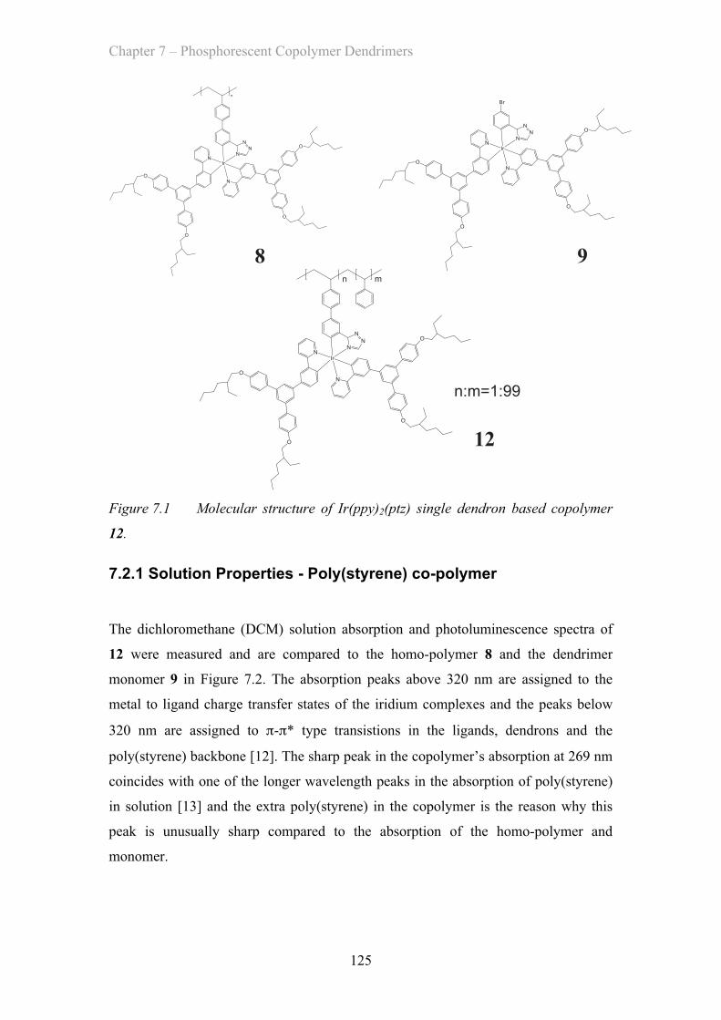
Chapter 7 – Phosphorescent Copolymer Dendrimers
125
12
n:m=1:99
8 9
Figure 7.1 Molecular structure of Ir(ppy)2(ptz) single dendron based copolymer
12.
7.2.1 Solution Properties - Poly(styrene) co-polymer
The dichloromethane (DCM) solution absorption and photoluminescence spectra of
12 were measured and are compared to the homo-polymer 8 and the dendrimer
monomer 9 in Figure 7.2. The absorption peaks above 320 nm are assigned to the
metal to ligand charge transfer states of the iridium complexes and the peaks below
320 nm are assigned to π-π* type transistions in the ligands, dendrons and the
poly(styrene) backbone [12]. The sharp peak in the copolymer’s absorption at 269 nm
coincides with one of the longer wavelength peaks in the absorption of poly(styrene)
in solution [13] and the extra poly(styrene) in the copolymer is the reason why this
peak is unusually sharp compared to the absorption of the homo-polymer and
monomer.
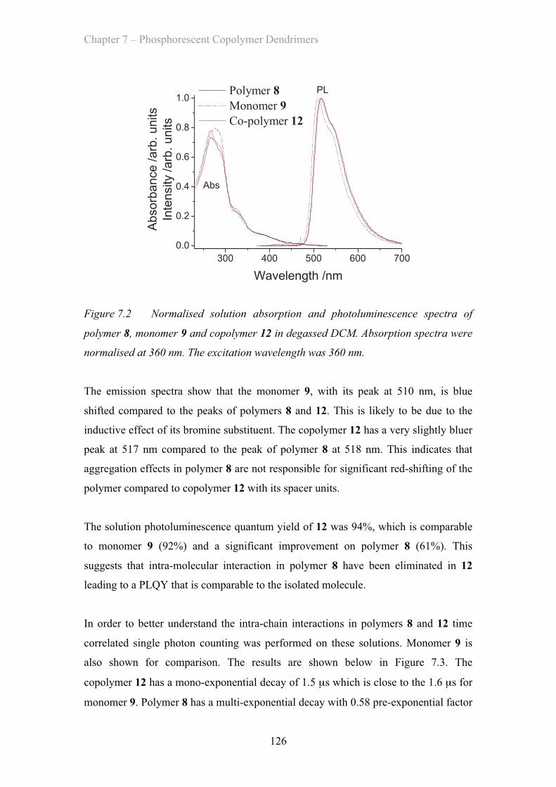
Chapter 7 – Phosphorescent Copolymer Dendrimers
126
Figure 7.2 Normalised solution absorption and photoluminescence spectra of
polymer 8, monomer 9 and copolymer 12 in degassed DCM. Absorption spectra were
normalised at 360 nm. The excitation wavelength was 360 nm.
The emission spectra show that the monomer 9, with its peak at 510 nm, is blue
shifted compared to the peaks of polymers 8 and 12. This is likely to be due to the
inductive effect of its bromine substituent. The copolymer 12 has a very slightly bluer
peak at 517 nm compared to the peak of polymer 8 at 518 nm. This indicates that
aggregation effects in polymer 8 are not responsible for significant red-shifting of the
polymer compared to copolymer 12 with its spacer units.
The solution photoluminescence quantum yield of 12 was 94%, which is comparable
to monomer 9 (92%) and a significant improvement on polymer 8 (61%). This
suggests that intra-molecular interaction in polymer 8 have been eliminated in 12
leading to a PLQY that is comparable to the isolated molecule.
In order to better understand the intra-chain interactions in polymers 8 and 12 time
correlated single photon counting was performed on these solutions. Monomer 9 is
also shown for comparison. The results are shown below in Figure 7.3. The
copolymer 12 has a mono-exponential decay of 1.5 µs which is close to the 1.6 µs for
monomer 9. Polymer 8 has a multi-exponential decay with 0.58 pre-exponential factor
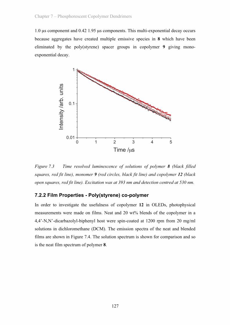
Chapter 7 – Phosphorescent Copolymer Dendrimers
127
1.0 µs componemt and 0.42 1.95 µs components. This multi-exponential decay occurs
because aggregates have created multiple emissive species in 8 which have been
eliminated by the poly(styrene) spacer groups in copolymer 9 giving mono-
exponential decay.
0 1 2 3 4 50.01
0.1
1
Inte
nsity
/arb
. units
Time /µs
Figure 7.3 Time resolved luminescence of solutions of polymer 8 (black filled
squares, red fit line), monomer 9 (red circles, black fit line) and copolymer 12 (black
open squares, red fit line). Excitation was at 393 nm and detection centred at 530 nm.
7.2.2 Film Properties - Poly(styrene) co-polymer
In order to investigate the usefulness of copolymer 12 in OLEDs, photophysical
measurements were made on films. Neat and 20 wt% blends of the copolymer in a
4,4’-N,N’-dicarbazolyl-biphenyl host were spin-coated at 1200 rpm from 20 mg/ml
solutions in dichloromethane (DCM). The emission spectra of the neat and blended
films are shown in Figure 7.4. The solution spectrum is shown for comparison and so
is the neat film spectrum of polymer 8.
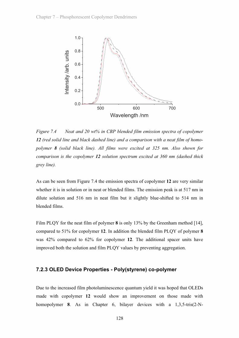
Chapter 7 – Phosphorescent Copolymer Dendrimers
128
500 600 7000.0
0.2
0.4
0.6
0.8
1.0
Inte
nsity
/arb
. units
Wavelength /nm
Figure 7.4 Neat and 20 wt% in CBP blended film emission spectra of copolymer
12 (red solid line and black dashed line) and a comparison with a neat film of homo-
polymer 8 (solid black line). All films were excited at 325 nm. Also shown for
comparison is the copolymer 12 solution spectrum excited at 360 nm (dashed thick
grey line).
As can be seen from Figure 7.4 the emission spectra of copolymer 12 are very similar
whether it is in solution or in neat or blended films. The emission peak is at 517 nm in
dilute solution and 516 nm in neat film but it slightly blue-shifted to 514 nm in
blended films.
Film PLQY for the neat film of polymer 8 is only 13% by the Greenham method [14],
compared to 51% for copolymer 12. In addition the blended film PLQY of polymer 8
was 42% compared to 62% for copolymer 12. The additional spacer units have
improved both the solution and film PLQY values by preventing aggregation.
7.2.3 OLED Device Properties - Poly(styrene) co-polymer
Due to the increased film photoluminescence quantum yield it was hoped that OLEDs
made with copolymer 12 would show an improvement on those made with
homopolymer 8. As in Chapter 6, bilayer devices with a 1,3,5-tris(2-N-
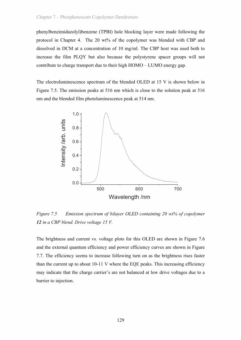
Chapter 7 – Phosphorescent Copolymer Dendrimers
129
phenylbenzimidazolyl)benzene (TPBI) hole blocking layer were made following the
protocol in Chapter 4. The 20 wt% of the copolymer was blended with CBP and
dissolved in DCM at a concentration of 10 mg/ml. The CBP host was used both to
increase the film PLQY but also because the polystyrene spacer groups will not
contribute to charge transport due to their high HOMO – LUMO energy gap.
The electroluminescence spectrum of the blended OLED at 15 V is shown below in
Figure 7.5. The emission peaks at 516 nm which is close to the solution peak at 516
nm and the blended film photoluminescence peak at 514 nm.
500 600 700
0.0
0.2
0.4
0.6
0.8
1.0
Inte
nsity /arb
. units
Wavelength /nm
Figure 7.5 Emission spectrum of bilayer OLED containing 20 wt% of copolymer
12 in a CBP blend. Drive voltage 15 V.
The brightness and current vs. voltage plots for this OLED are shown in Figure 7.6
and the external quantum efficiency and power efficiency curves are shown in Figure
7.7. The efficiency seems to increase following turn on as the brightness rises faster
than the current up to about 10-11 V where the EQE peaks. This increasing efficiency
may indicate that the charge carrier’s are not balanced at low drive voltages due to a
barrier to injection.
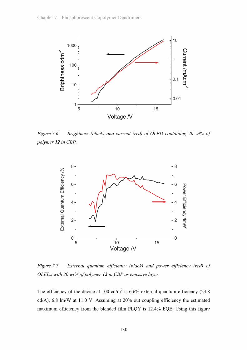
Chapter 7 – Phosphorescent Copolymer Dendrimers
130
5 10 151
10
100
1000
0.01
0.1
1
10
Curre
nt /m
Acm
-2B
rightn
ess c
dm
-2
Voltage /V
Figure 7.6 Brightness (black) and current (red) of OLED containing 20 wt% of
polymer 12 in CBP.
5 10 150
2
4
6
8
0
2
4
6
8
Po
we
r Effic
ien
cy /lm
W-1E
xte
rna
l Q
ua
ntu
m E
ffic
ien
cy /
%
Voltage /V
Figure 7.7 External quantum efficiency (black) and power efficiency (red) of
OLEDs with 20 wt% of polymer 12 in CBP as emissive layer.
The efficiency of the device at 100 cd/m2 is 6.6% external quantum efficiency (23.8
cd/A), 6.8 lm/W at 11.0 V. Assuming at 20% out coupling efficiency the estimated
maximum efficiency from the blended film PLQY is 12.4% EQE. Using this figure
Chapter 7 – Phosphorescent Copolymer Dendrimers
131
these devices are operating about 50% of optimal efficiency. It is likely that this is
because charge balance has not been achieved, perhaps because the poly(styrene)
units are reducing hole transport through the emissive layer. These results are,
however, an improvement on homopolymer 8 blended film devices which achieved
100 cd/m2 at 6.2% EQE (21.8 cd/A) and 13.2 V. This is because the copolymer has
achieved an increased blended film PLQY due to its spacer units which reduce inter-
molecular and intra-molecular aggregation effects.
7.3 Poly(carbazole) copolymers In order to try and produce better copolymer materials for devices it was decided to
try and use charge transporting spacer units to separate the emissive units. As many
charge transport materials used in OLEDs contain the carbazol moiety [15] the
decision was taken to use 9-vinylcarbazole as the spacer unit. When used to form a
homo-polymer, poly(9-vinylcarbazole), this material is often known as PVK or PVCz
and is commonly used as a hole transport material [15, 16]. It was decided to try these
materials without dendrons, with single dendrons and with double dendrons to see
what effect this had on aggregation.
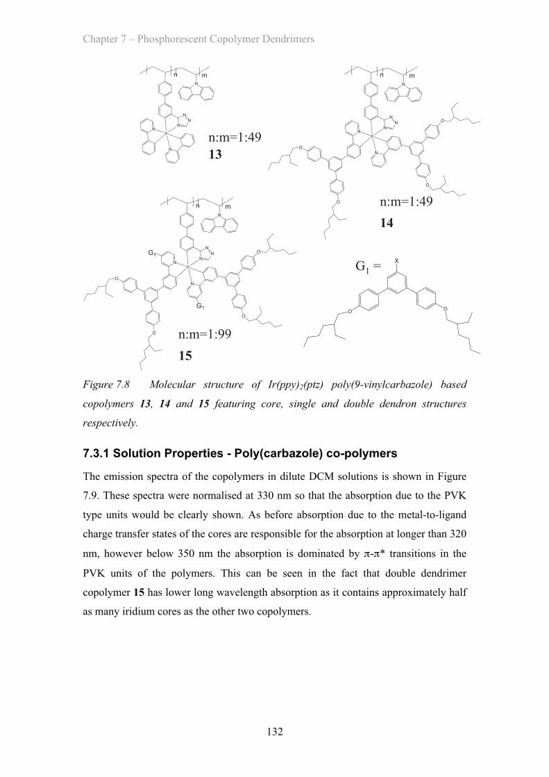
Chapter 7 – Phosphorescent Copolymer Dendrimers
132
14
13
15
n:m=1:49
n:m=1:49
n:m=1:99
G1 =
Figure 7.8 Molecular structure of Ir(ppy)2(ptz) poly(9-vinylcarbazole) based
copolymers 13, 14 and 15 featuring core, single and double dendron structures
respectively.
7.3.1 Solution Properties - Poly(carbazole) co-polymers
The emission spectra of the copolymers in dilute DCM solutions is shown in Figure
7.9. These spectra were normalised at 330 nm so that the absorption due to the PVK
type units would be clearly shown. As before absorption due to the metal-to-ligand
charge transfer states of the cores are responsible for the absorption at longer than 320
nm, however below 350 nm the absorption is dominated by π-π* transitions in the
PVK units of the polymers. This can be seen in the fact that double dendrimer
copolymer 15 has lower long wavelength absorption as it contains approximately half
as many iridium cores as the other two copolymers.
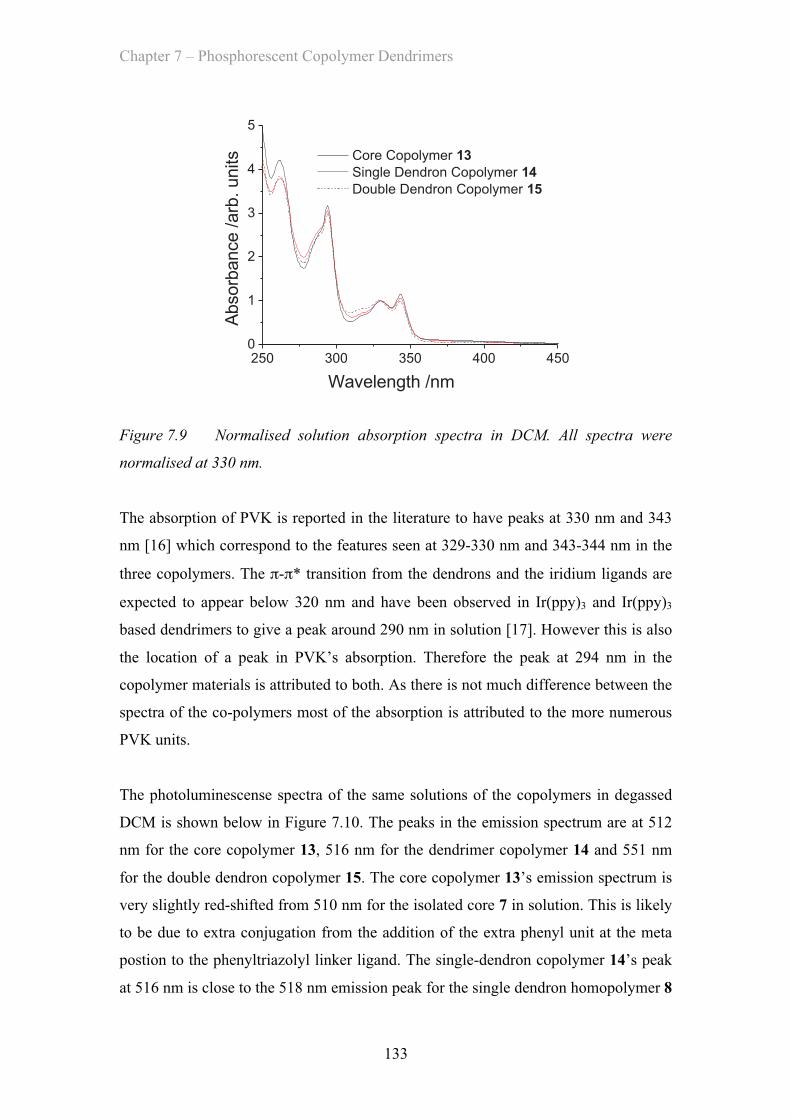
Chapter 7 – Phosphorescent Copolymer Dendrimers
133
250 300 350 400 4500
1
2
3
4
5
Core Copolymer 13 Single Dendron Copolymer 14 Double Dendron Copolymer 15
Absorb
ance /arb
. units
Wavelength /nm
Figure 7.9 Normalised solution absorption spectra in DCM. All spectra were
normalised at 330 nm.
The absorption of PVK is reported in the literature to have peaks at 330 nm and 343
nm [16] which correspond to the features seen at 329-330 nm and 343-344 nm in the
three copolymers. The π-π* transition from the dendrons and the iridium ligands are
expected to appear below 320 nm and have been observed in Ir(ppy)3 and Ir(ppy)3
based dendrimers to give a peak around 290 nm in solution [17]. However this is also
the location of a peak in PVK’s absorption. Therefore the peak at 294 nm in the
copolymer materials is attributed to both. As there is not much difference between the
spectra of the co-polymers most of the absorption is attributed to the more numerous
PVK units.
The photoluminescense spectra of the same solutions of the copolymers in degassed
DCM is shown below in Figure 7.10. The peaks in the emission spectrum are at 512
nm for the core copolymer 13, 516 nm for the dendrimer copolymer 14 and 551 nm
for the double dendron copolymer 15. The core copolymer 13’s emission spectrum is
very slightly red-shifted from 510 nm for the isolated core 7 in solution. This is likely
to be due to extra conjugation from the addition of the extra phenyl unit at the meta
postion to the phenyltriazolyl linker ligand. The single-dendron copolymer 14’s peak
at 516 nm is close to the 518 nm emission peak for the single dendron homopolymer 8
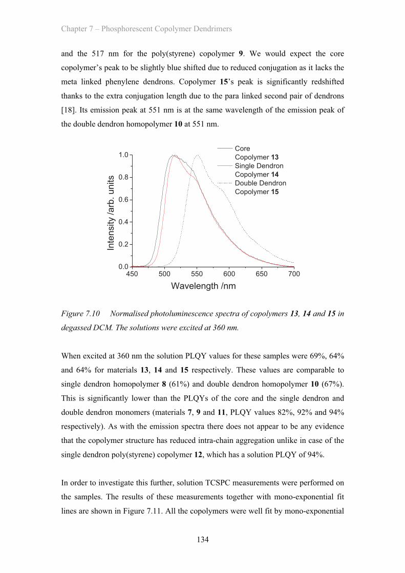
Chapter 7 – Phosphorescent Copolymer Dendrimers
134
and the 517 nm for the poly(styrene) copolymer 9. We would expect the core
copolymer’s peak to be slightly blue shifted due to reduced conjugation as it lacks the
meta linked phenylene dendrons. Copolymer 15’s peak is significantly redshifted
thanks to the extra conjugation length due to the para linked second pair of dendrons
[18]. Its emission peak at 551 nm is at the same wavelength of the emission peak of
the double dendron homopolymer 10 at 551 nm.
450 500 550 600 650 7000.0
0.2
0.4
0.6
0.8
1.0 Core
Copolymer 13 Single Dendron
Copolymer 14 Double Dendron
Copolymer 15
Inte
nsity /arb
. units
Wavelength /nm
Figure 7.10 Normalised photoluminescence spectra of copolymers 13, 14 and 15 in
degassed DCM. The solutions were excited at 360 nm.
When excited at 360 nm the solution PLQY values for these samples were 69%, 64%
and 64% for materials 13, 14 and 15 respectively. These values are comparable to
single dendron homopolymer 8 (61%) and double dendron homopolymer 10 (67%).
This is significantly lower than the PLQYs of the core and the single dendron and
double dendron monomers (materials 7, 9 and 11, PLQY values 82%, 92% and 94%
respectively). As with the emission spectra there does not appear to be any evidence
that the copolymer structure has reduced intra-chain aggregation unlike in case of the
single dendron poly(styrene) copolymer 12, which has a solution PLQY of 94%.
In order to investigate this further, solution TCSPC measurements were performed on
the samples. The results of these measurements together with mono-exponential fit
lines are shown in Figure 7.11. All the copolymers were well fit by mono-exponential
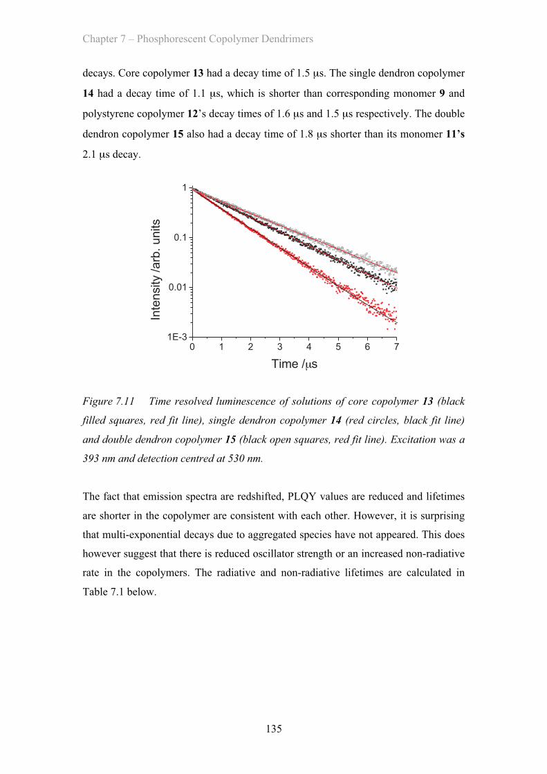
Chapter 7 – Phosphorescent Copolymer Dendrimers
135
decays. Core copolymer 13 had a decay time of 1.5 µs. The single dendron copolymer
14 had a decay time of 1.1 µs, which is shorter than corresponding monomer 9 and
polystyrene copolymer 12’s decay times of 1.6 µs and 1.5 µs respectively. The double
dendron copolymer 15 also had a decay time of 1.8 µs shorter than its monomer 11’s
2.1 µs decay.
0 1 2 3 4 5 6 71E-3
0.01
0.1
1
Inte
nsity /arb
. units
Time /µs
Figure 7.11 Time resolved luminescence of solutions of core copolymer 13 (black
filled squares, red fit line), single dendron copolymer 14 (red circles, black fit line)
and double dendron copolymer 15 (black open squares, red fit line). Excitation was a
393 nm and detection centred at 530 nm.
The fact that emission spectra are redshifted, PLQY values are reduced and lifetimes
are shorter in the copolymer are consistent with each other. However, it is surprising
that multi-exponential decays due to aggregated species have not appeared. This does
however suggest that there is reduced oscillator strength or an increased non-radiative
rate in the copolymers. The radiative and non-radiative lifetimes are calculated in
Table 7.1 below.
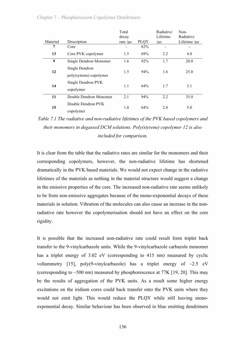
Chapter 7 – Phosphorescent Copolymer Dendrimers
136
Material Description
Total decay rate /µs PLQY
Radiative Lifetime /µs
Non-Radiative Lifetime /µs
7 Core - 82% - -
13 Core PVK copolymer 1.5 69% 2.2 4.8
9 Single Dendron Monomer 1.6 92% 1.7 20.0
12 Single Dendron
poly(sytrene) copolymer 1.5 94% 1.6 25.0
14 Single Dendron PVK
copolymer 1.1 64% 1.7 3.1
11 Double Dendron Monomer 2.1 94% 2.2 35.0
15 Double Dendron PVK
copolymer 1.8 64% 2.8 5.0
Table 7.1 The radiative and non-radiative lifetimes of the PVK based copolymers and
their monomers in degassed DCM solutions. Poly(styrene) copolymer 12 is also
included for comparison.
It is clear from the table that the radiative rates are similar for the monomers and their
corresponding copolymers, however, the non-radiative lifetime has shortened
dramatically in the PVK based materials. We would not expect change in the radiative
lifetimes of the materials as nothing in the material structure would suggest a change
in the emissive properties of the core. The increased non-radiative rate seems unlikely
to be from non-emissive aggregates because of the mono-exponential decays of these
materials in solution. Vibration of the molecules can also cause an increase in the non-
radiative rate however the copolymerisation should not have an effect on the core
rigidity.
It is possible that the increased non-radiative rate could result form triplet back
transfer to the 9-vinylcarbazole units. While the 9-vinylcarbazole carbazole monomer
has a triplet energy of 3.02 eV (corresponding to 415 nm) measured by cyclic
voltammetry [15], poly(9-vinylcarbazole) has a triplet energy of ~2.5 eV
(corresponding to ~500 nm) measured by phosphorescence at 77K [19, 20]. This may
be the results of aggregation of the PVK units. As a result some higher energy
excitations on the iridium cores could back transfer onto the PVK units where they
would not emit light. This would reduce the PLQY while still leaving mono-
exponential decay. Similar behaviour has been observed in blue emitting dendrimers
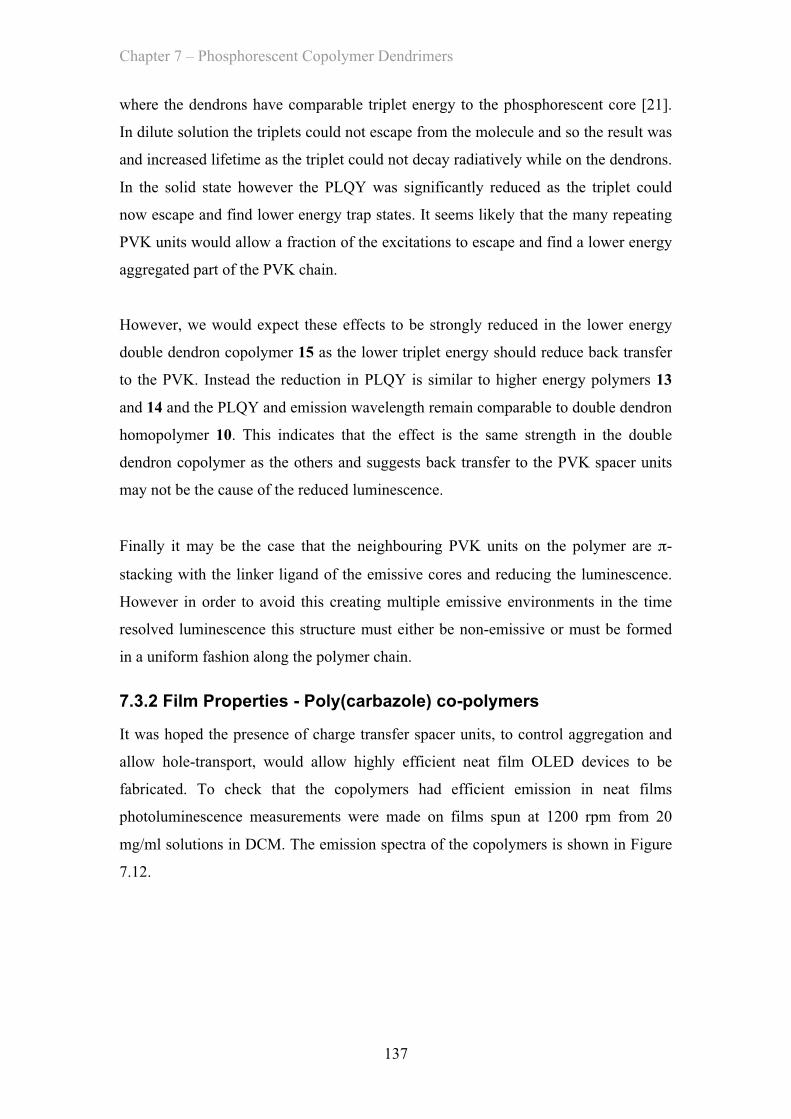
Chapter 7 – Phosphorescent Copolymer Dendrimers
137
where the dendrons have comparable triplet energy to the phosphorescent core [21].
In dilute solution the triplets could not escape from the molecule and so the result was
and increased lifetime as the triplet could not decay radiatively while on the dendrons.
In the solid state however the PLQY was significantly reduced as the triplet could
now escape and find lower energy trap states. It seems likely that the many repeating
PVK units would allow a fraction of the excitations to escape and find a lower energy
aggregated part of the PVK chain.
However, we would expect these effects to be strongly reduced in the lower energy
double dendron copolymer 15 as the lower triplet energy should reduce back transfer
to the PVK. Instead the reduction in PLQY is similar to higher energy polymers 13
and 14 and the PLQY and emission wavelength remain comparable to double dendron
homopolymer 10. This indicates that the effect is the same strength in the double
dendron copolymer as the others and suggests back transfer to the PVK spacer units
may not be the cause of the reduced luminescence.
Finally it may be the case that the neighbouring PVK units on the polymer are π-
stacking with the linker ligand of the emissive cores and reducing the luminescence.
However in order to avoid this creating multiple emissive environments in the time
resolved luminescence this structure must either be non-emissive or must be formed
in a uniform fashion along the polymer chain.
7.3.2 Film Properties - Poly(carbazole) co-polymers
It was hoped the presence of charge transfer spacer units, to control aggregation and
allow hole-transport, would allow highly efficient neat film OLED devices to be
fabricated. To check that the copolymers had efficient emission in neat films
photoluminescence measurements were made on films spun at 1200 rpm from 20
mg/ml solutions in DCM. The emission spectra of the copolymers is shown in Figure
7.12.
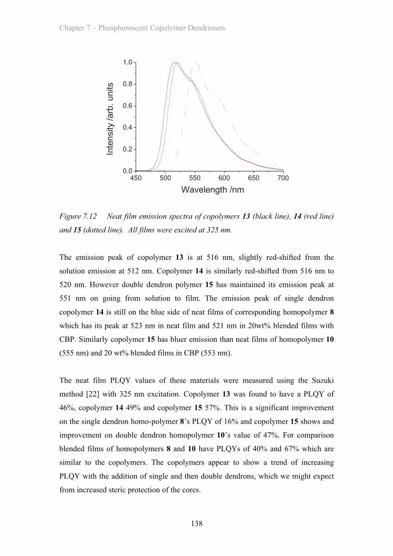
Chapter 7 – Phosphorescent Copolymer Dendrimers
138
450 500 550 600 650 7000.0
0.2
0.4
0.6
0.8
1.0
Inte
nsity
/arb
. units
Wavelength /nm
Figure 7.12 Neat film emission spectra of copolymers 13 (black line), 14 (red line)
and 15 (dotted line). All films were excited at 325 nm.
The emission peak of copolymer 13 is at 516 nm, slightly red-shifted from the
solution emission at 512 nm. Copolymer 14 is similarly red-shifted from 516 nm to
520 nm. However double dendron polymer 15 has maintained its emission peak at
551 nm on going from solution to film. The emission peak of single dendron
copolymer 14 is still on the blue side of neat films of corresponding homopolymer 8
which has its peak at 523 nm in neat film and 521 nm in 20wt% blended films with
CBP. Similarly copolymer 15 has bluer emission than neat films of homopolymer 10
(555 nm) and 20 wt% blended films in CBP (553 nm).
The neat film PLQY values of these materials were measured using the Suzuki
method [22] with 325 nm excitation. Copolymer 13 was found to have a PLQY of
46%, copolymer 14 49% and copolymer 15 57%. This is a significant improvement
on the single dendron homo-polymer 8’s PLQY of 16% and copolymer 15 shows and
improvement on double dendron homopolymer 10’s value of 47%. For comparison
blended films of homopolymers 8 and 10 have PLQYs of 40% and 67% which are
similar to the copolymers. The copolymers appear to show a trend of increasing
PLQY with the addition of single and then double dendrons, which we might expect
from increased steric protection of the cores.
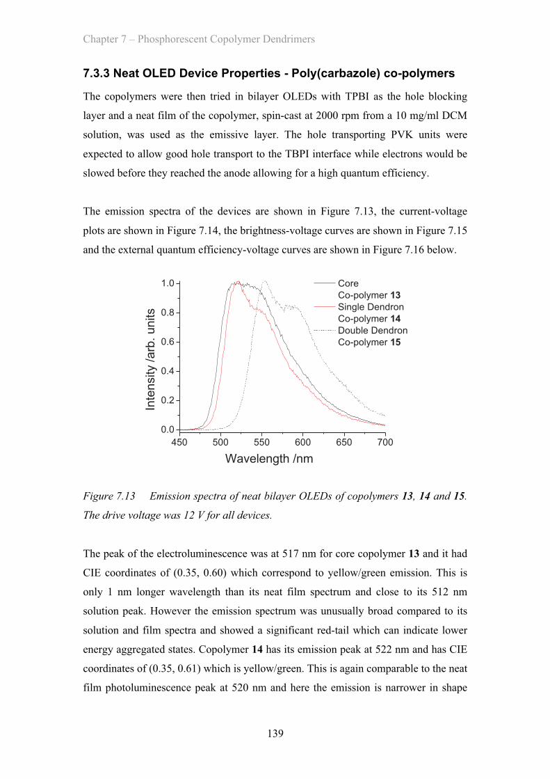
Chapter 7 – Phosphorescent Copolymer Dendrimers
139
7.3.3 Neat OLED Device Properties - Poly(carbazole) co-polymers
The copolymers were then tried in bilayer OLEDs with TPBI as the hole blocking
layer and a neat film of the copolymer, spin-cast at 2000 rpm from a 10 mg/ml DCM
solution, was used as the emissive layer. The hole transporting PVK units were
expected to allow good hole transport to the TBPI interface while electrons would be
slowed before they reached the anode allowing for a high quantum efficiency.
The emission spectra of the devices are shown in Figure 7.13, the current-voltage
plots are shown in Figure 7.14, the brightness-voltage curves are shown in Figure 7.15
and the external quantum efficiency-voltage curves are shown in Figure 7.16 below.
450 500 550 600 650 700
0.0
0.2
0.4
0.6
0.8
1.0 Core
Co-polymer 13 Single Dendron
Co-polymer 14 Double Dendron
Co-polymer 15
Inte
nsity /arb
. units
Wavelength /nm
Figure 7.13 Emission spectra of neat bilayer OLEDs of copolymers 13, 14 and 15.
The drive voltage was 12 V for all devices.
The peak of the electroluminescence was at 517 nm for core copolymer 13 and it had
CIE coordinates of (0.35, 0.60) which correspond to yellow/green emission. This is
only 1 nm longer wavelength than its neat film spectrum and close to its 512 nm
solution peak. However the emission spectrum was unusually broad compared to its
solution and film spectra and showed a significant red-tail which can indicate lower
energy aggregated states. Copolymer 14 has its emission peak at 522 nm and has CIE
coordinates of (0.35, 0.61) which is yellow/green. This is again comparable to the neat
film photoluminescence peak at 520 nm and here the emission is narrower in shape
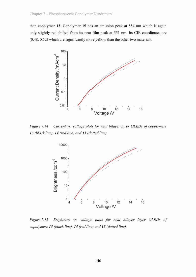
Chapter 7 – Phosphorescent Copolymer Dendrimers
140
than copolymer 13. Copolymer 15 has an emission peak at 554 nm which is again
only slightly red-shifted from its neat film peak at 551 nm. Its CIE coordinates are
(0.48, 0.52) which are significantly more yellow than the other two materials.
4 6 8 10 12 14 160.01
0.1
1
10
100
Curr
ent D
ensity /m
Acm
-2
Voltage /V
Figure 7.14 Current vs. voltage plots for neat bilayer layer OLEDs of copolymers
13 (black line), 14 (red line) and 15 (dotted line).
4 6 8 10 12 14 161
10
100
1000
10000
Brightn
ess /cdm
-2
Voltage /V
Figure 7.15 Brightness vs. voltage plots for neat bilayer layer OLEDs of
copolymers 13 (black line), 14 (red line) and 15 (dotted line).
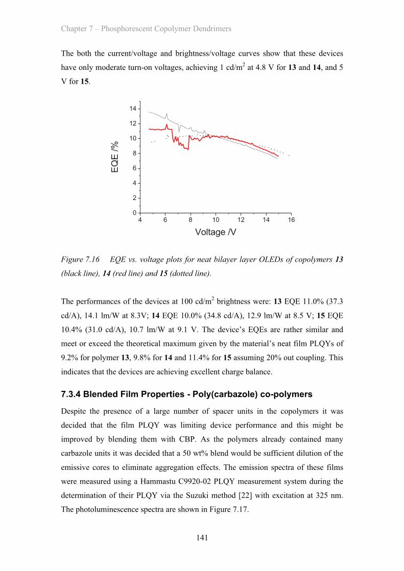
Chapter 7 – Phosphorescent Copolymer Dendrimers
141
The both the current/voltage and brightness/voltage curves show that these devices
have only moderate turn-on voltages, achieving 1 cd/m2 at 4.8 V for 13 and 14, and 5
V for 15.
4 6 8 10 12 14 160
2
4
6
8
10
12
14E
QE
/%
Voltage /V
Figure 7.16 EQE vs. voltage plots for neat bilayer layer OLEDs of copolymers 13
(black line), 14 (red line) and 15 (dotted line).
The performances of the devices at 100 cd/m2 brightness were: 13 EQE 11.0% (37.3
cd/A), 14.1 lm/W at 8.3V; 14 EQE 10.0% (34.8 cd/A), 12.9 lm/W at 8.5 V; 15 EQE
10.4% (31.0 cd/A), 10.7 lm/W at 9.1 V. The device’s EQEs are rather similar and
meet or exceed the theoretical maximum given by the material’s neat film PLQYs of
9.2% for polymer 13, 9.8% for 14 and 11.4% for 15 assuming 20% out coupling. This
indicates that the devices are achieving excellent charge balance.
7.3.4 Blended Film Properties - Poly(carbazole) co-polymers
Despite the presence of a large number of spacer units in the copolymers it was
decided that the film PLQY was limiting device performance and this might be
improved by blending them with CBP. As the polymers already contained many
carbazole units it was decided that a 50 wt% blend would be sufficient dilution of the
emissive cores to eliminate aggregation effects. The emission spectra of these films
were measured using a Hammastu C9920-02 PLQY measurement system during the
determination of their PLQY via the Suzuki method [22] with excitation at 325 nm.
The photoluminescence spectra are shown in Figure 7.17.
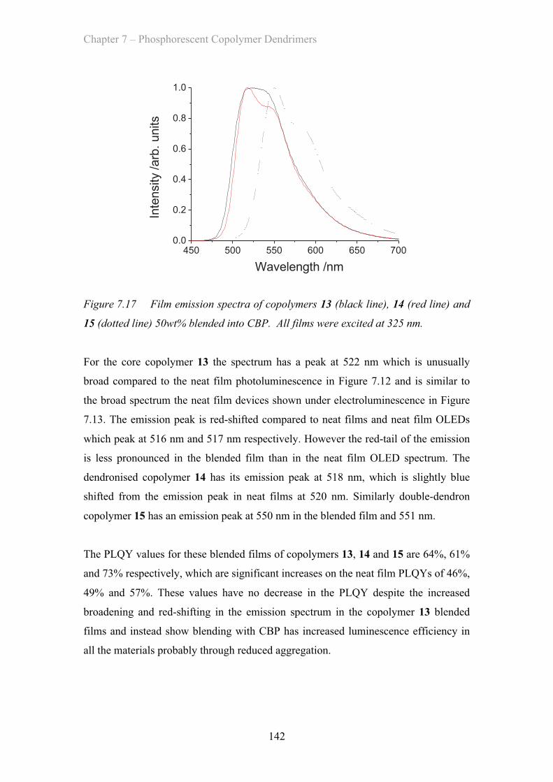
Chapter 7 – Phosphorescent Copolymer Dendrimers
142
450 500 550 600 650 7000.0
0.2
0.4
0.6
0.8
1.0
Inte
nsity
/arb
. units
Wavelength /nm
Figure 7.17 Film emission spectra of copolymers 13 (black line), 14 (red line) and
15 (dotted line) 50wt% blended into CBP. All films were excited at 325 nm.
For the core copolymer 13 the spectrum has a peak at 522 nm which is unusually
broad compared to the neat film photoluminescence in Figure 7.12 and is similar to
the broad spectrum the neat film devices shown under electroluminescence in Figure
7.13. The emission peak is red-shifted compared to neat films and neat film OLEDs
which peak at 516 nm and 517 nm respectively. However the red-tail of the emission
is less pronounced in the blended film than in the neat film OLED spectrum. The
dendronised copolymer 14 has its emission peak at 518 nm, which is slightly blue
shifted from the emission peak in neat films at 520 nm. Similarly double-dendron
copolymer 15 has an emission peak at 550 nm in the blended film and 551 nm.
The PLQY values for these blended films of copolymers 13, 14 and 15 are 64%, 61%
and 73% respectively, which are significant increases on the neat film PLQYs of 46%,
49% and 57%. These values have no decrease in the PLQY despite the increased
broadening and red-shifting in the emission spectrum in the copolymer 13 blended
films and instead show blending with CBP has increased luminescence efficiency in
all the materials probably through reduced aggregation.
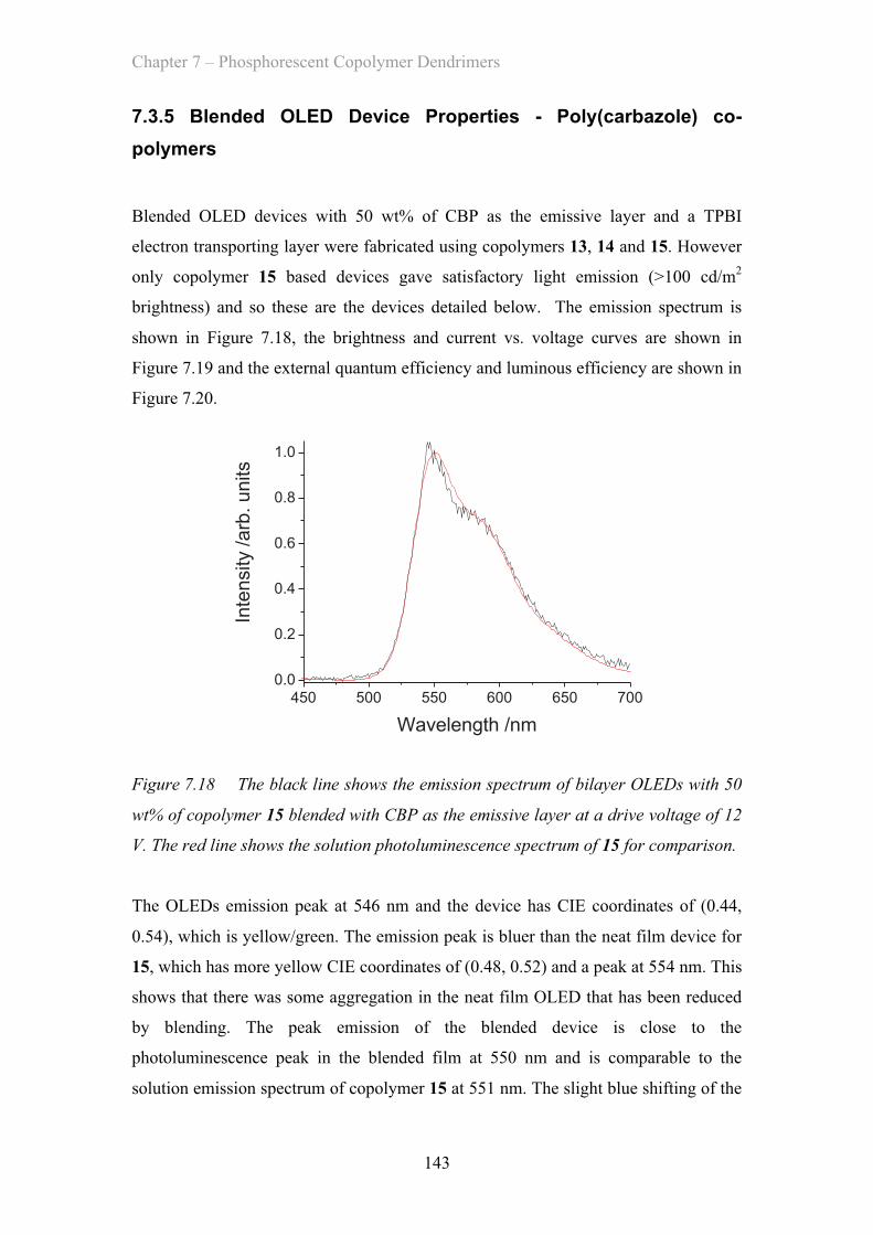
Chapter 7 – Phosphorescent Copolymer Dendrimers
143
7.3.5 Blended OLED Device Properties - Poly(carbazole) co-polymers
Blended OLED devices with 50 wt% of CBP as the emissive layer and a TPBI
electron transporting layer were fabricated using copolymers 13, 14 and 15. However
only copolymer 15 based devices gave satisfactory light emission (>100 cd/m2
brightness) and so these are the devices detailed below. The emission spectrum is
shown in Figure 7.18, the brightness and current vs. voltage curves are shown in
Figure 7.19 and the external quantum efficiency and luminous efficiency are shown in
Figure 7.20.
450 500 550 600 650 700
0.0
0.2
0.4
0.6
0.8
1.0
Inte
nsity /arb
. units
Wavelength /nm
Figure 7.18 The black line shows the emission spectrum of bilayer OLEDs with 50
wt% of copolymer 15 blended with CBP as the emissive layer at a drive voltage of 12
V. The red line shows the solution photoluminescence spectrum of 15 for comparison.
The OLEDs emission peak at 546 nm and the device has CIE coordinates of (0.44,
0.54), which is yellow/green. The emission peak is bluer than the neat film device for
15, which has more yellow CIE coordinates of (0.48, 0.52) and a peak at 554 nm. This
shows that there was some aggregation in the neat film OLED that has been reduced
by blending. The peak emission of the blended device is close to the
photoluminescence peak in the blended film at 550 nm and is comparable to the
solution emission spectrum of copolymer 15 at 551 nm. The slight blue shifting of the
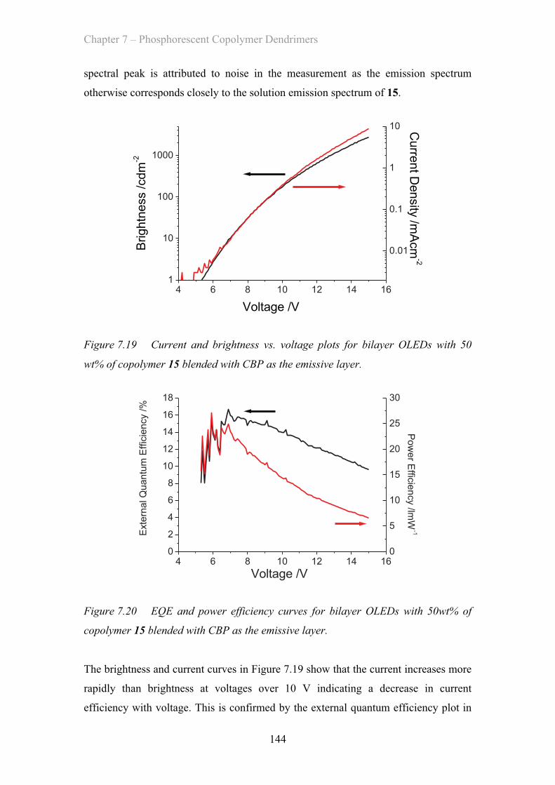
Chapter 7 – Phosphorescent Copolymer Dendrimers
144
spectral peak is attributed to noise in the measurement as the emission spectrum
otherwise corresponds closely to the solution emission spectrum of 15.
4 6 8 10 12 14 161
10
100
1000
0.01
0.1
1
10 Curre
nt D
ensity
/mA
cm
-2B
rightn
ess /cdm
-2
Voltage /V
Figure 7.19 Current and brightness vs. voltage plots for bilayer OLEDs with 50
wt% of copolymer 15 blended with CBP as the emissive layer.
4 6 8 10 12 14 160
2
4
6
8
10
12
14
16
18
0
5
10
15
20
25
30
Po
we
r Effic
ien
cy /lm
W-1E
xte
rna
l Q
ua
ntu
m E
ffic
ien
cy /
%
Voltage /V
Figure 7.20 EQE and power efficiency curves for bilayer OLEDs with 50wt% of
copolymer 15 blended with CBP as the emissive layer.
The brightness and current curves in Figure 7.19 show that the current increases more
rapidly than brightness at voltages over 10 V indicating a decrease in current
efficiency with voltage. This is confirmed by the external quantum efficiency plot in
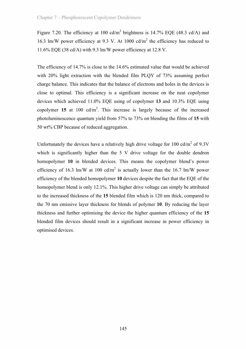
Chapter 7 – Phosphorescent Copolymer Dendrimers
145
Figure 7.20. The efficiency at 100 cd/m2 brightness is 14.7% EQE (48.3 cd/A) and
16.3 lm/W power efficiency at 9.3 V. At 1000 cd/m2 the efficiency has reduced to
11.6% EQE (38 cd/A) with 9.3 lm/W power efficiency at 12.8 V.
The efficiency of 14.7% is close to the 14.6% estimated value that would be achieved
with 20% light extraction with the blended film PLQY of 73% assuming perfect
charge balance. This indicates that the balance of electrons and holes in the devices is
close to optimal. This efficiency is a significant increase on the neat copolymer
devices which achieved 11.0% EQE using of copolymer 13 and 10.3% EQE using
copolymer 15 at 100 cd/m2. This increase is largely because of the increased
photoluminescence quantum yield from 57% to 73% on blending the films of 15 with
50 wt% CBP because of reduced aggregation.
Unfortunately the devices have a relatively high drive voltage for 100 cd/m2 of 9.3V
which is significantly higher than the 5 V drive voltage for the double dendron
homopolymer 10 in blended devices. This means the copolymer blend’s power
efficiency of 16.3 lm/W at 100 cd/m2 is actually lower than the 16.7 lm/W power
efficiency of the blended homopolymer 10 devices despite the fact that the EQE of the
homopolymer blend is only 12.1%. This higher drive voltage can simply be attributed
to the increased thickness of the 15 blended film which is 120 nm thick, compared to
the 70 nm emissive layer thickness for blends of polymer 10. By reducing the layer
thickness and further optimising the device the higher quantum efficiency of the 15
blended film devices should result in a significant increase in power efficiency in
optimised devices.
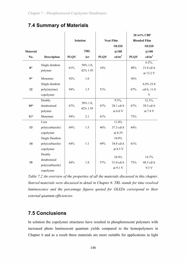
Chapter 7 – Phosphorescent Copolymer Dendrimers
146
7.4 Summary of Materials
Material
No. Description
Solution Neat Film
20 wt% CBP
Blended Film
PLQY
TRL
/µµs PLQY
OLED
@100
cd/m2 PLQY
OLED
@100
cd/m2
8* Single dendron
polymer 61%
58% 1.0,
42% 1.95 16% 40%
6.2%,
21.8 cd/A
at 13.2 V
9* Monomer 92% 1.6 56%
12
Single dendron
poly(styrene)
copolymer
94% 1.5 51% 67%
6.6% 23.8
cd/A, 11.0
V
10*
Doubly
dendronised
polymer
67% 58% 1.0,
42% 1.95 47%
9.3%,
28.1 cd/A
at 6.0 V
67%
12.1%,
39.3 cd/A
at 7.4 V
11* Monomer 94% 2.1 41% 73%
13
Core
poly(carbazole)
copolymer
69% 1.5 46%
11.0%
37.3 cd/A
at 8.3V
64%
14
Single Dendron
poly(carbazole)
copolymer
64% 1.1 49%
10.0%
34.8 cd/A
at 8.5 V
61%
15
Doubly
dendronised
poly(carbazole)
copolymer
64% 1.8 57%
10.4%
31.0 cd/A
at 9.1 V
73%
14.7%
48.3 cd/A
9.3 V
Table 7.2 An overview of the properties of all the materials discussed in this chapter.
Starred materials were discussed in detail in Chapter 6. TRL stands for time resolved
luminescence and the percentage figures quoted for OLEDs correspond to their
external quantum efficiencies.
7.5 Conclusions In solution the copolymer structures have resulted in phosphorescent polymers with
increased photo luminescent quantum yields compared to the homopolymers in
Chapter 6 and as a result these materials are more suitable for applications in light
Chapter 7 – Phosphorescent Copolymer Dendrimers
147
emitting diodes. This has been demonstrated by the fabrication of devices with higher
external quantum efficiencies than in comparable homo-polymers, achieving a
maximum efficiency of 14.7% at 100 cd/m2. This result is significantly higher than
the previous best reported quantum efficiency for a phosphorescent polymer of 11.8%
[5].
The improvement in solution quantum yields can be seen most clearly in copolymer
12, with its poly(styrene) spacer units and single dendron emissive core. In this
material the addition of the spacer groups have increased the PLQY from 61% for,
comparable homopolymer 8, to 94% which is comparable to the monomer’s PLQY of
92%. This lack of intra-chain interactions is confirmed by the mono-exponential
photoluminescence lifetime.
Copolymer 12 remained impressive in films, showing significant improvements over
polymer 8, giving 51% PLQY in neat film and 67% in blended films of 12 compared
to only 16% and 40% for 8. However the polystyrene spacer units were effectively
insulating and appear to have impeded hole transport in blended bilayer OLED
devices resulting in a EQE of 6.6% at 100 cd/m2, approximately 50% of the estimated
maximum given the blended film PLQY. While this was better than 6.2% EQE for
polymer 8 it suggested that copolymers with hole transporting units might be better
for devices.
Using poly(carbazole) as the spacer units met the requirement of high energy hole
transporting spacer units. However the photoluminescence quantum yields of these
materials in film were less promising at only 61%-69%, compared to >90% for the
monomers and the poly(styrene) spacer copolymer. Time resolved luminescence
showed that the materials did have mono-exponential decays, indicating only one
emissive state was present, but that they had increased non-radiative decay rates
without changing the radiative rates. This suggests that the poly(carbazole) units have
in some way provided a non-radiative de-excitation pathway in these materials.
Fortunately the poly(carbazole) materials did not suffer a significant decrease in
photoluminescence quantum yield in neat or blended films, which set the upper limit
on OLED efficiency. By controlling intra-core interactions through the use of the
Chapter 7 – Phosphorescent Copolymer Dendrimers
148
carbazole units and dendrons these materials gave 11.0% EQE in neat films and
14.7% EQE (48.3 cd/A) in blended films at 100 cd/m2. This is a significant
improvement on using double dendrons to control interactions in a homopolymer
alone which only gave 9.0% and 12.1% EQE respectively. This makes means this
device has a significantly higher current efficiency than the 11.8% EQE [5] or 35.1
cd/A [10] of the best literature reports for a phosphorescent polymer.
It is unclear that the dendon’s have made a significant improvement to the
performance of these materials as the neat and blended film PLQYs of the core only,
single dendron and double dendron materials are similar. There is however a slight
upward trend with increasing number of dendrons from 46%, 49% to 57% in neat film
and 64%, 61%, 73% in blended film. Critically it appears that the double dendron
structure has allowed the creation of high brightness OLEDs when blended with CBP,
which was not the case for the other two materials. The combination of double
dendrons and the poly(carbazole) spacer units in copolymer 15 has resulted in the
highest blended film PLQY of any of any of the materials presented in Chapter 6 or 7
and this has lead to its very high OLED external quantum efficiency which
corresponds to an estimated internal quantum efficiency of ~75% in a solution
processable device.
1. Chen, X.W., et al., High-efficiency red-light emission from polyfluorenes grafted with cyclometalated iridium complexes and charge transport moiety. Journal of the American Chemical Society, 2003. 125(3): p. 636-637.
2. Sudhakar, M., et al., Phosphorescence quenching by conjugated polymers. Journal of the American Chemical Society, 2003. 125(26): p. 7796-7797.
3. Tokito, S., M. Suzuki, and F. Sato, Improvement of emission efficiency in polymer light-emitting devices based on phosphorescent polymers. Thin Solid Films, 2003. 445: p. 353–357.
4. Tokito, S., et al., High-efficiency phosphorescent polymer light-emitting devices. Organic Electronics, 2003. 4: p. 105–111.
5. Suzuki, M., et al., Highly efficient polymer light-emitting devices using ambipolar phosphorescent polymers. Applied Physics Letters, 2005. 86(10): p. 103507.
6. Sandee, A.J., et al., Solution-processible conjugated electrophosphorescent polymers. Journal of the American Chemical Society, 2004. 126(22): p. 7041-7048.
7. Jiang, J.X., et al., High-efficiency electrophosphorescent fluorene-alt-carbazole copolymers N-grafted with cyclometalated Ir complexes. Macromolecules, 2005. 38(10): p. 4072-4080.
Chapter 7 – Phosphorescent Copolymer Dendrimers
149
8. Zhen, H.Y., et al., Electrophosphorescent chelating copolymers based on linkage isomers of naphthylpyridine-iridium complexes with fluorene. Macromolecules, 2006. 39(5): p. 1693-1700.
9. Jiang, J.X., et al., High-efficiency white-light-emitting devices from a single polymer by mixing singlet and triplet emission. Advanced Materials, 2006. 18(13): p. 1769-+.
10. Thesen, M.W., et al., Hole-Transporting Host-Polymer Series Consisting of Triphenylamine Basic Structures for Phosphorescent Polymer Light-Emitting Diodes. Journal of Polymer Science Part a-Polymer Chemistry, 2010. 48(15): p. 3417-3430.
11. Thesen, M.W., et al., Investigation of Spacer Influences in Phosphorescent-Emitting Nonconjugated PLED Systems. Journal of Polymer Science Part a-Polymer Chemistry, 2010. 48(2): p. 389-402.
12. Hay, P.J., Theoretical studies of the ground and excited electronic states in cyclometalated phenylpyridine Ir(III) complexes using density functional theory. Journal of Physical Chemistry A, 2002. 106(8): p. 1634-1641.
13. Torkelson, J.M., et al., Fluorescence and Absorbance of Polystyrene in Dilute and Semidilute Solutions. Macromolecules, 1983. 16(2): p. 326-330.
14. Greenham, N.C., et al., Measurement of Absolute Photoluminescence Quantum Efficiencies in Conjugated Polymers. Chemical Physics Letters, 1995. 241(1-2): p. 89-96.
15. Brunner, K., et al., Carbazole compounds as host materials for triplet emitters in organic light-emitting diodes: Tuning the HOMO level without influencing the triplet energy in small molecules. Journal of the American Chemical Society, 2004. 126(19): p. 6035-6042.
16. Zhang, C., et al., Blue Electroluminescent Diodes Utilizing Blends of Poly(p-phenylphenylene vinylene) in Poly(9-vinylcarbazoyl). Synthetic Metals, 1994. 62(1): p. 35-40.
17. Namdas, E.B., et al., Photophysics of Fac-tris(2-phenylpyridine) iridium(III) cored electroluminescent dendrimers in solution and films. Journal of Physical Chemistry B, 2004. 108(5): p. 1570-1577.
18. Lo, S.C., et al., Encapsulated cores: Host-free organic light-emitting diodes based on solution-processible electrophosphorescent dendrimers. Advanced Materials, 2005. 17(16): p. 1945-+.
19. Kawamura, Y., S. Yanagida, and S.R. Forrest, Energy transfer in polymer electrophosphorescent light emitting devices with single and multiple doped luminescent layers. Journal of Applied Physics, 2002. 92(1): p. 87-93.
20. Rippen, G., G. Kaufmann, and W. Klopffer, Luminescence of Poly(n-vinylcarbazole) Films at 77K. Fluorescence, Phosphorescence and Delayed Fluorescence. Chemical Physics, 1980. 52(1-2): p. 165-177.
21. Lo, S.C., et al., High-Triplet-Energy Dendrons: Enhancing the Luminescence of Deep Blue Phosphorescent Iridium(III) Complexes. Journal of the American Chemical Society, 2009. 131(46): p. 16681-16688.
22. Suzuki, K., et al., Reevaluation of absolute luminescence quantum yields of standard solutions using a spectrometer with an integrating sphere and a back-thinned CCD detector. Physical Chemistry Chemical Physics, 2009. 11(42): p. 9850-9860.
150
8. UV Enhanced Hybrid Photodiodes
8.1 Introduction .......................................................................................................... 150�8.2 Photodiode Fabrication and Testing .................................................................... 152�8.3 Results .................................................................................................................. 154�
8.3.1 Poly(fluorene) Enhancement Layer .......................................................... 154�8.3.2 (F8)9BT Co-polymer Enhancement Layer ................................................ 156�8.3.3 (F8)9BT CBP Blend Enhancement Layer ................................................. 158�
8.4 Modelling ............................................................................................................. 161�8.5 Conclusions .......................................................................................................... 167�
8.1 Introduction
Chapters 5 to 7 have focused on light emitting materials and devices, however in this
chapter I will focus on using organic semiconductors in devices for detecting light. A
commonly used technology for light detection in the visible uses silicon p-n junctions.
This has high sensitivity in the visible at relatively low cost while being directly
compatible with silicon CMOS processing technologies. This has allowed a
proliferation of low cost multi-pixel visible imaging technologies like CCDs which
can be used in applications from taking pictures to compact multi-channel
spectrometers.
Unfortunately, silicon detectors work best in the visible and near infra-red and do not
have sensitivity in the ultraviolet (UV). These wavelengths are useful for applications
in spectroscopy [1], astronomy [2] and nuclear physics [3]. Silicon’s low UV response
is due to its of the high refractive index and the strong absorption of silicon at these
wavelengths. This means that much incident light is reflected and the rest absorbed in
the first few nanometers away from the p-n junction, where electron and holes can be
separated and converted into photocurrent. The refractive index and absorption
coefficient of intrinsic silicon are shown in Figure 8.1 (taken from the publication by
Green and Keevers [4]).
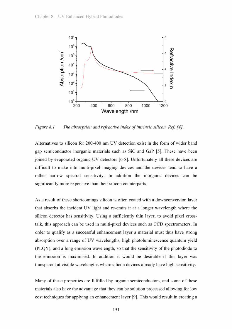
Chapter 8 – UV Enhanced Hybrid Photodiodes
151
200 400 600 800 1000 120010
0
101
102
103
104
105
106
107
0
2
4
6
8
Refra
ctiv
e In
dex nA
bsorp
tion /cm
-1
Wavelength /nm
Figure 8.1 The absorption and refractive index of intrinsic silicon. Ref. [4].
Alternatives to silicon for 200-400 nm UV detection exist in the form of wider band
gap semiconductor inorganic materials such as SiC and GaP [5]. These have been
joined by evaporated organic UV detectors [6-8]. Unfortunately all these devices are
difficult to make into multi-pixel imaging devices and the devices tend to have a
rather narrow spectral sensitivity. In addition the inorganic devices can be
significantly more expensive than their silicon counterparts.
As a result of these shortcomings silicon is often coated with a downconversion layer
that absorbs the incident UV light and re-emits it at a longer wavelength where the
silicon detector has sensitivity. Using a sufficiently thin layer, to avoid pixel cross-
talk, this approach can be used in multi-pixel devices such as CCD spectrometers. In
order to qualify as a successful enhancement layer a material must thus have strong
absorption over a range of UV wavelengths, high photoluminescence quantum yield
(PLQY), and a long emission wavelength, so that the sensitivity of the photodiode to
the emission is maximised. In addition it would be desirable if this layer was
transparent at visible wavelengths where silicon devices already have high sensitivity.
Many of these properties are fulfilled by organic semiconductors, and some of these
materials also have the advantage that they can be solution processed allowing for low
cost techniques for applying an enhancement layer [9]. This would result in creating a
Chapter 8 – UV Enhanced Hybrid Photodiodes
152
“hybrid” device, which uses both organic and inorganic materials [10]. Organic
enhancement layers that have been tried in the past, but have mostly been deposited
by the relatively high cost method of thermal evaporation. Materials that have been
reported included aluminum tris-8-hydroxyquinoline (Alq3), N,N’-diphenyl-N,N’-bis-
(3-methylphenl)-1,1’-biphenyl-4,4’-diamine, and bis-(8-hydroxyquinaldine)-
chlorogallium (Gaq2’Cl) [11], lumogen and coronene [12-14]. Evaporated lumogen
(which is commonly used in sensitising commercial CCDs) achieves 20-30%
quantum efficiency across the UV, and coronene has achieved 30-40% efficiency.
Though some patent literature has reported the idea of using the solution processable
organic semiconducting polymer poly[2,7-(9,9-dioctylfluorene)] (PFO) [15] the
responsivity of this device was still observed to fall by a factor of 100 from 500 nm to
250 nm indicating that this early effort was not very successful. Therefore I decided to
see if it was possible to improve on these results.
In Section 8.2 I will discuss the experimental methods used in this chapter. In Section
8.3 I will discuss the absorption and luminescence properties of the enhancement
layers used and their effect on the performance of photodiodes. Section 8.4 will focus
on a simple model that can be used to explain the response of UV photodiodes given
the optical and photophysical properties of the enhancement layer. Finally the
conclusions are presented in Section 8.5.
8.2 Photodiode Fabrication and Testing The photodiodes used for enhancement in this experiment were Silonex SLSD-71N5
photodiodes. These were chosen because they were not encapsulated and so the
enhancement layer could be directly spin coated on top of the transparent silicon
oxide layer on top of the devices. This layer was found to be 68 nm thick using a J.A.
Woolam Co. Inc. M-2000DI spectrosoptic ellipsometer. It provided good wetting
properties and did not interfere with light coupling into the device. The enhancement
layers were spin coated from toluene or dicholoromethane solutions directly on top of
the photodiodes for device performance and reflectivity measurements and onto
quartz discs for absorption and photoluminescence measurements. Film thickness
measurements were made using a Veeco DekTak 150 surface profilometer.
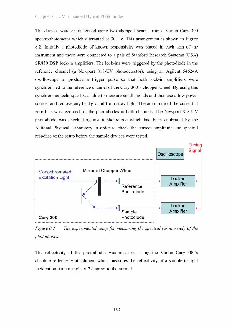
Chapter 8 – UV Enhanced Hybrid Photodiodes
153
The devices were characterised using two chopped beams from a Varian Cary 300
spectrophotometer which alternated at 30 Hz. This arrangement is shown in Figure
8.2. Initially a photodiode of known responsivity was placed in each arm of the
instrument and these were connected to a pair of Stanford Research Systems (USA)
SR830 DSP lock-in amplifiers. The lock-ins were triggered by the photodiode in the
reference channel (a Newport 818-UV photodetector), using an Agilent 54624A
oscilloscope to produce a trigger pulse so that both lock-in amplifiers were
synchronised to the reference channel of the Cary 300’s chopper wheel. By using this
synchronous technique I was able to measure small signals and thus use a low power
source, and remove any background from stray light. The amplitude of the current at
zero bias was recorded for the photodiodes in both channels. The Newport 818-UV
photodiode was checked against a photodiode which had been calibrated by the
National Physical Laboratory in order to check the correct amplitude and spectral
response of the setup before the sample devices were tested.
Mirrored Chopper WheelMonochromated
Excitation Light
Reference
Photodiode
Sample
PhotodiodeCary 300
Lock-in
Amplifier
Lock-in
Amplifier
Oscilloscope
Timing
Signal
Figure 8.2 The experimental setup for measuring the spectral responsively of the
photodiodes.
The reflectivity of the photodiodes was measured using the Varian Cary 300’s
absolute reflectivity attachment which measures the reflectivity of a sample to light
incident on it at an angle of 7 degrees to the normal.

Chapter 8 – UV Enhanced Hybrid Photodiodes
154
8.3 Results
8.3.1 Poly(fluorene) Enhancement Layer
The chemical structure of poly[2,7-(9,9-dioctylfluorene)] (PFO) [16-18] is shown in
Figure 8.3. This material is a commonly used blue light emitting polymer with a good
photoluminescence quantum yield of around 50% in thin films [18]. Therefore, PFO
seemed a suitable candidate for a solution processable enhancement layer. The PFO
used in these measurements was ADS129BE purchased from American Dye Source.
In all cases below the PFO films were spin coated from toluene solutions at a
concentration of 10 mg/ml at 2000 rpm. The absorption and emission spectra of the
material is shown in Figure 8.4. The quantum efficiency of devices enhanced using a
53 nm film PFO is shown in Figure 8.5.
Figure 8.3 Molecular Structure of poly[2,7-(9,9-dioctylfluorene)](PFO).
200 300 400 500 6000.0
0.1
0.2
0.3
0.4
0.5
0.6
0.7
0.8
0.9
1.0
Ab
so
rptio
n /
ab
s.
No
rma
lise
d I
nte
nsity /
arb
. u
nits
Wavelength /nm
Figure 8.4 Absorption and emission spectra of a 53 nm thick film of PFO. The
emission spectrum was excited at 325 nm.
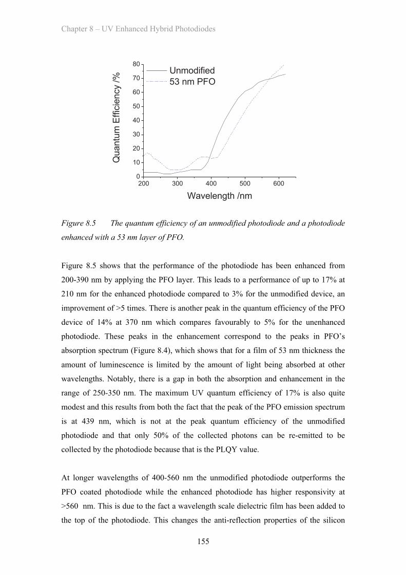
Chapter 8 – UV Enhanced Hybrid Photodiodes
155
200 300 400 500 6000
10
20
30
40
50
60
70
80 Unmodified
53 nm PFO
Quantu
m E
ffic
iency /%
Wavelength /nm
Figure 8.5 The quantum efficiency of an unmodified photodiode and a photodiode
enhanced with a 53 nm layer of PFO.
Figure 8.5 shows that the performance of the photodiode has been enhanced from
200-390 nm by applying the PFO layer. This leads to a performance of up to 17% at
210 nm for the enhanced photodiode compared to 3% for the unmodified device, an
improvement of >5 times. There is another peak in the quantum efficiency of the PFO
device of 14% at 370 nm which compares favourably to 5% for the unenhanced
photodiode. These peaks in the enhancement correspond to the peaks in PFO’s
absorption spectrum (Figure 8.4), which shows that for a film of 53 nm thickness the
amount of luminescence is limited by the amount of light being absorbed at other
wavelengths. Notably, there is a gap in both the absorption and enhancement in the
range of 250-350 nm. The maximum UV quantum efficiency of 17% is also quite
modest and this results from both the fact that the peak of the PFO emission spectrum
is at 439 nm, which is not at the peak quantum efficiency of the unmodified
photodiode and that only 50% of the collected photons can be re-emitted to be
collected by the photodiode because that is the PLQY value.
At longer wavelengths of 400-560 nm the unmodified photodiode outperforms the
PFO coated photodiode while the enhanced photodiode has higher responsivity at
>560 nm. This is due to the fact a wavelength scale dielectric film has been added to
the top of the photodiode. This changes the anti-reflection properties of the silicon
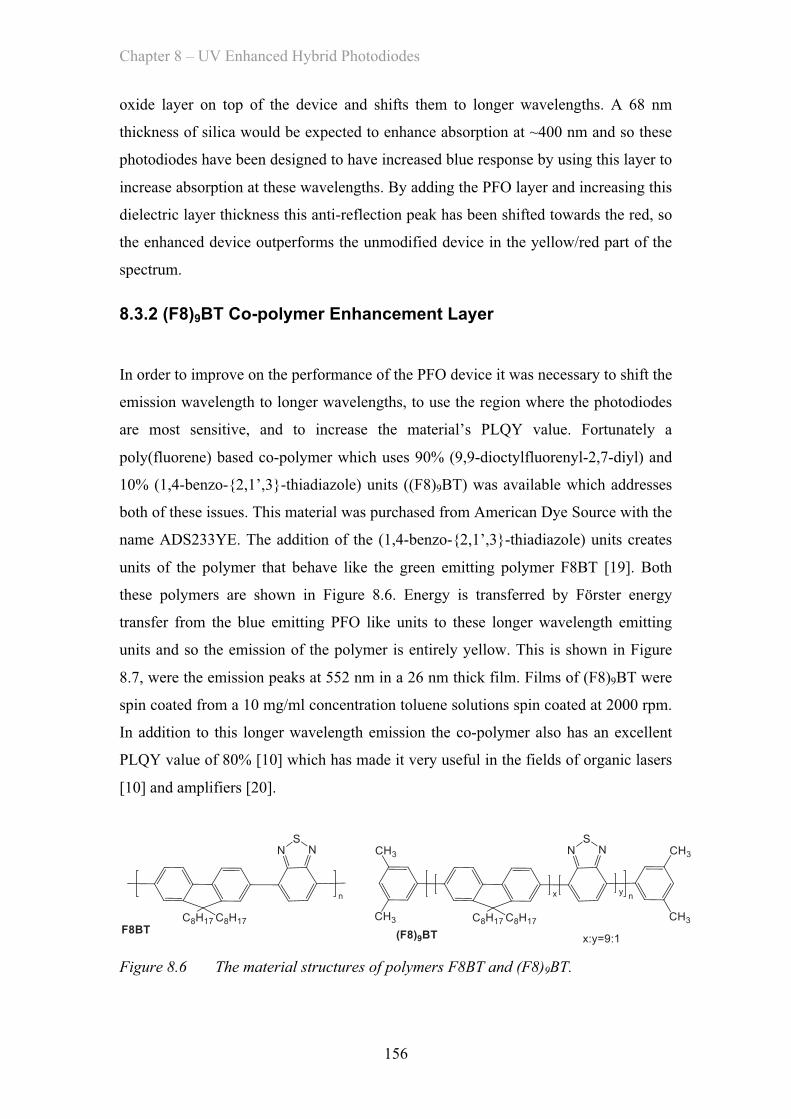
Chapter 8 – UV Enhanced Hybrid Photodiodes
156
oxide layer on top of the device and shifts them to longer wavelengths. A 68 nm
thickness of silica would be expected to enhance absorption at ~400 nm and so these
photodiodes have been designed to have increased blue response by using this layer to
increase absorption at these wavelengths. By adding the PFO layer and increasing this
dielectric layer thickness this anti-reflection peak has been shifted towards the red, so
the enhanced device outperforms the unmodified device in the yellow/red part of the
spectrum.
8.3.2 (F8)9BT Co-polymer Enhancement Layer
In order to improve on the performance of the PFO device it was necessary to shift the
emission wavelength to longer wavelengths, to use the region where the photodiodes
are most sensitive, and to increase the material’s PLQY value. Fortunately a
poly(fluorene) based co-polymer which uses 90% (9,9-dioctylfluorenyl-2,7-diyl) and
10% (1,4-benzo-{2,1’,3}-thiadiazole) units ((F8)9BT) was available which addresses
both of these issues. This material was purchased from American Dye Source with the
name ADS233YE. The addition of the (1,4-benzo-{2,1’,3}-thiadiazole) units creates
units of the polymer that behave like the green emitting polymer F8BT [19]. Both
these polymers are shown in Figure 8.6. Energy is transferred by Förster energy
transfer from the blue emitting PFO like units to these longer wavelength emitting
units and so the emission of the polymer is entirely yellow. This is shown in Figure
8.7, were the emission peaks at 552 nm in a 26 nm thick film. Films of (F8)9BT were
spin coated from a 10 mg/ml concentration toluene solutions spin coated at 2000 rpm.
In addition to this longer wavelength emission the co-polymer also has an excellent
PLQY value of 80% [10] which has made it very useful in the fields of organic lasers
[10] and amplifiers [20].
Figure 8.6 The material structures of polymers F8BT and (F8)9BT.
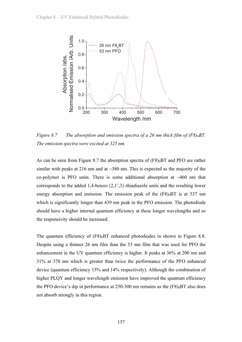
Chapter 8 – UV Enhanced Hybrid Photodiodes
157
200 300 400 500 600 7000.0
0.2
0.4
0.6
0.8
1.0
Absorp
tion /abs.
Norm
alis
ed E
mis
sio
n /A
rb. U
nits
Wavelength /nm
26 nm F89BT
53 nm PFO
Figure 8.7 The absorption and emission spectra of a 26 nm thick film of (F8)9BT.
The emission spectra were excited at 325 nm.
As can be seen from Figure 8.7 the absorption spectra of (F8)9BT and PFO are rather
similar with peaks at 216 nm and at ~380 nm. This is expected as the majority of the
co-polymer is PFO units. There is some additional absorption at ~460 nm that
corresponds to the added 1,4-benzo-{2,1’,3}-thiadiazole units and the resulting lower
energy absorption and emission. The emission peak of the (F8)9BT is at 537 nm
which is significantly longer than 439 nm peak in the PFO emission. The photodiode
should have a higher internal quantum efficiency at these longer wavelengths and so
the responsivity should be increased.
The quantum efficiency of (F8)9BT enhanced photodiodes in shown in Figure 8.8.
Despite using a thinner 26 nm film than the 53 nm film that was used for PFO the
enhancement in the UV quantum efficiency is higher. It peaks at 36% at 200 nm and
31% at 370 nm which is greater than twice the performance of the PFO enhanced
device (quantum efficiency 15% and 14% respectively). Although the combination of
higher PLQY and longer wavelength emission have improved the quantum efficiency
the PFO device’s dip in performance at 250-300 nm remains as the (F8)9BT also does
not absorb strongly in this region.
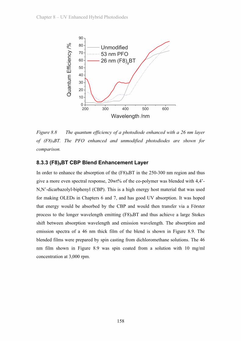
Chapter 8 – UV Enhanced Hybrid Photodiodes
158
200 300 400 500 6000
10
20
30
40
50
60
70
80
90
Unmodified
53 nm PFO
26 nm (F8)9BT
Quantu
m E
ffic
iency /%
Wavelength /nm
Figure 8.8 The quantum efficiency of a photodiode enhanced with a 26 nm layer
of (F8)9BT. The PFO enhanced and unmodified photodiodes are shown for
comparison.
8.3.3 (F8)9BT CBP Blend Enhancement Layer
In order to enhance the absorption of the (F8)9BT in the 250-300 nm region and thus
give a more even spectral response, 20wt% of the co-polymer was blended with 4,4’-
N,N’-dicarbazolyl-biphenyl (CBP). This is a high energy host material that was used
for making OLEDs in Chapters 6 and 7, and has good UV absorption. It was hoped
that energy would be absorbed by the CBP and would then transfer via a Förster
process to the longer wavelength emitting (F8)9BT and thus achieve a large Stokes
shift between absorption wavelength and emission wavelength. The absorption and
emission spectra of a 46 nm thick film of the blend is shown in Figure 8.9. The
blended films were prepared by spin casting from dichloromethane solutions. The 46
nm film shown in Figure 8.9 was spin coated from a solution with 10 mg/ml
concentration at 3,000 rpm.
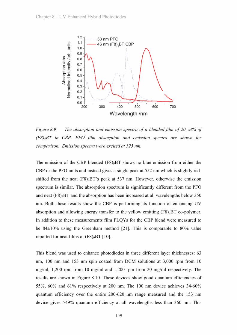
Chapter 8 – UV Enhanced Hybrid Photodiodes
159
200 300 400 500 600 7000.0
0.1
0.2
0.3
0.4
0.5
0.6
0.7
0.8
0.9
1.0
1.1
1.2 53 nm PFO
46 nm (F8)9BT:CBP
Ab
so
rptio
n /
ab
s.
No
rma
lise
d I
nte
nsity /
arb
. u
nits
Wavelength /nm
Figure 8.9 The absorption and emission spectra of a blended film of 20 wt% of
(F8)9BT in CBP. PFO film absorption and emission spectra are shown for
comparison. Emission spectra were excited at 325 nm.
The emission of the CBP blended (F8)9BT shows no blue emission from either the
CBP or the PFO units and instead gives a single peak at 552 nm which is slightly red-
shifted from the neat (F8)9BT’s peak at 537 nm. However, otherwise the emission
spectrum is similar. The absorption spectrum is significantly different from the PFO
and neat (F8)9BT and the absorption has been increased at all wavelengths below 350
nm. Both these results show the CBP is performing its function of enhancing UV
absorption and allowing energy transfer to the yellow emitting (F8)9BT co-polymer.
In addition to these measurements film PLQYs for the CBP blend were measured to
be 84±10% using the Greenham method [21]. This is comparable to 80% value
reported for neat films of (F8)9BT [10].
This blend was used to enhance photodiodes in three different layer thicknesses: 63
nm, 100 nm and 153 nm spin coated from DCM solutions at 3,000 rpm from 10
mg/ml, 1,200 rpm from 10 mg/ml and 1,200 rpm from 20 mg/ml respectively. The
results are shown in Figure 8.10. These devices show good quantum efficiencies of
55%, 60% and 61% respectively at 200 nm. The 100 nm device achieves 34-60%
quantum efficiency over the entire 200-620 nm range measured and the 153 nm
device gives >49% quantum efficiency at all wavelengths less than 360 nm. This
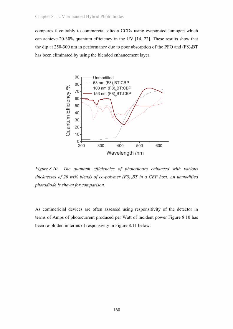
Chapter 8 – UV Enhanced Hybrid Photodiodes
160
compares favourably to commercial silicon CCDs using evaporated lumogen which
can achieve 20-30% quantum efficiency in the UV [14, 22]. These results show that
the dip at 250-300 nm in performance due to poor absorption of the PFO and (F8)9BT
has been eliminated by using the blended enhancement layer.
200 300 400 500 6000
10
20
30
40
50
60
70
80
90
Quantu
m E
ffic
iency /%
Wavelength /nm
Unmodified
63 nm (F8)9BT:CBP
100 nm (F8)9BT:CBP
153 nm (F8)9BT:CBP
Figure 8.10 The quantum efficiencies of photodiodes enhanced with various
thicknesses of 20 wt% blends of co-polymer (F8)9BT in a CBP host. An unmodified
photodiode is shown for comparison.
As commericial devices are often assessed using responsitivity of the detector in
terms of Amps of photocurrent produced per Watt of incident power Figure 8.10 has
been re-plotted in terms of responsivity in Figure 8.11 below.
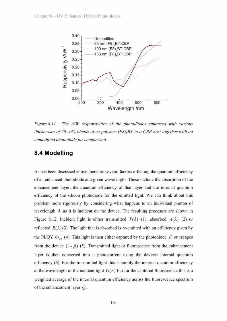
Chapter 8 – UV Enhanced Hybrid Photodiodes
161
200 300 400 500 6000.00
0.05
0.10
0.15
0.20
0.25
0.30
0.35
0.40
Responsiv
ity /A
W-1
Wavelength /nm
Unmodified
63 nm (F8)9BT:CBP
100 nm (F8)9BT:CBP
153 nm (F8)9BT:CBP
Figure 8.11 The A/W responsivities of the photodiodes enhanced with various
thicknesses of 20 wt% blends of co-polymer (F8)9BT in a CBP host together with an
unmodified photodiode for comparison.
8.4 Modelling
As has been discussed above there are several factors affecting the quantum efficiency
of an enhanced photodiode at a given wavelength. These include the absorption of the
enhancement layer, the quantum efficiency of that layer and the internal quantum
efficiency of the silicon photodiode for the emitted light. We can think about this
problem more rigorously by considering what happens to an individual photon of
wavelength λ as it is incident on the device. The resulting processes are shown in
Figure 8.12. Incident light is either transmitted )(λT (1), absorbed )(λA (2) or
reflected )(λR (3). The light that is absorbed is re-emitted with an efficiency given by
the PLQY PLΦ (4). This light is then either captured by the photodiode β or escapes
from the device )1( β− (5). Transmitted light or fluorescence from the enhancement
layer is then converted into a photocurrent using the devices internal quantum
efficiency (6). For the transmitted light this is simply the internal quantum efficiency
at the wavelength of the incident light )(λG but for the captured fluorescence this is a
weighted average of the internal quantum efficiency across the fluorescence spectrum
of the enhancement layer Q .
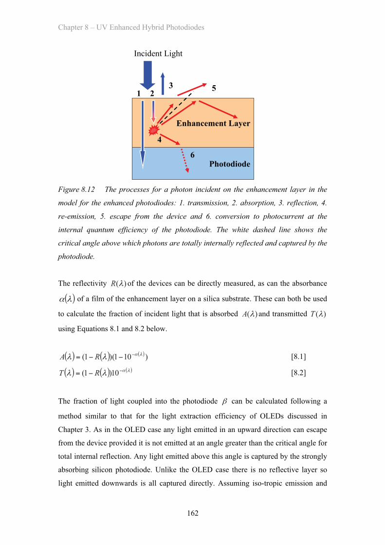
Chapter 8 – UV Enhanced Hybrid Photodiodes
162
Photodiode
Enhancement Layer
1 23
4
5
6
Incident Light
Figure 8.12 The processes for a photon incident on the enhancement layer in the
model for the enhanced photodiodes: 1. transmission, 2. absorption, 3. reflection, 4.
re-emission, 5. escape from the device and 6. conversion to photocurrent at the
internal quantum efficiency of the photodiode. The white dashed line shows the
critical angle above which photons are totally internally reflected and captured by the
photodiode.
The reflectivity )(λR of the devices can be directly measured, as can the absorbance
( )λα of a film of the enhancement layer on a silica substrate. These can both be used
to calculate the fraction of incident light that is absorbed )(λA and transmitted )(λT
using Equations 8.1 and 8.2 below.
( ) ( ) ( ))101)(1( λαλλ −−−= RA [8.1]
( ) ( ) ( )λαλλ −−= 10)1( RT [8.2]
The fraction of light coupled into the photodiode β can be calculated following a
method similar to that for the light extraction efficiency of OLEDs discussed in
Chapter 3. As in the OLED case any light emitted in an upward direction can escape
from the device provided it is not emitted at an angle greater than the critical angle for
total internal reflection. Any light emitted above this angle is captured by the strongly
absorbing silicon photodiode. Unlike the OLED case there is no reflective layer so
light emitted downwards is all captured directly. Assuming iso-tropic emission and
Chapter 8 – UV Enhanced Hybrid Photodiodes
163
performing an integral over all solid angles the fraction of light captured is given by
Equation 8.3. The refractive index of the CBP used in the enhanced photodiodes has a
refractive index of 1.75 at the wavelengths of the fluorescence, as determined from
previous elipsometry work [23]. Thus the fraction of captured light is estimated to be
91%.
⎟⎟⎠
⎞⎜⎜⎝
⎛−+=
2
111
2
1
nβ [8.3]
The internal quantum efficiency of the photodiode )(λG can be calculated by
dividing the external quantum efficiency ( )λBareE of the unmodified photodiode by
the fraction of incident light at a given wavelength that is absorbed ))(1( λBareR− .
Using this value the effective internal quantum efficiency of the photodiode to the
fluorescence of the enhancement layer Q can be calculated using the fluorescence
emission spectrum )(λL as shown in Equation 8.4.
∫∫=
λλ
λλλ
dL
dLGQ
)(
)()( [8.4]
Using all these contributions together the external quantum efficiency of the enhanced
photodiodes )(λE can be calculated using Equation 8.5.
( ) ( ) ( ) ( )λλβλλ GTQAE PL +Φ= [8.5]
Overall this method is similar to that used by Garbozov [11] however unlike their
reported method, this one does not split the spectrum into two parts based on the point
at which the internal quantum efficiency becomes negligible and takes transmitted
light into account across the entire spectrum.
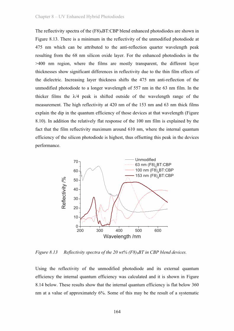
Chapter 8 – UV Enhanced Hybrid Photodiodes
164
The reflectivity spectra of the (F8)9BT:CBP blend enhanced photodiodes are shown in
Figure 8.13. There is a minimum in the reflectivity of the unmodified photodiode at
475 nm which can be attributed to the anti-reflection quarter wavelength peak
resulting from the 68 nm silicon oxide layer. For the enhanced photodiodes in the
>400 nm region, where the films are mostly transparent, the different layer
thicknesses show significant differences in reflectivity due to the thin film effects of
the dielectric. Increasing layer thickness shifts the 475 nm anti-reflection of the
unmodified photodiode to a longer wavelength of 557 nm in the 63 nm film. In the
thicker films the λ/4 peak is shifted outside of the wavelength range of the
measurement. The high reflectivity at 420 nm of the 153 nm and 63 nm thick films
explain the dip in the quantum efficiency of those devices at that wavelength (Figure
8.10). In addition the relatively flat response of the 100 nm film is explained by the
fact that the film reflectivity maximum around 610 nm, where the internal quantum
efficiency of the silicon photodiode is highest, thus offsetting this peak in the devices
performance.
200 300 400 500 6000
10
20
30
40
50
60
70
Reflectivity /%
Wavelength /nm
Unmodified
63 nm (F8)9BT:CBP
100 nm (F8)9BT:CBP
153 nm (F8)9BT:CBP
Figure 8.13 Reflectivity spectra of the 20 wt% (F8)9BT in CBP blend devices.
Using the reflectivity of the unmodified photodiode and its external quantum
efficiency the internal quantum efficiency was calculated and it is shown in Figure
8.14 below. These results show that the internal quantum efficiency is flat below 360
nm at a value of approximately 6%. Some of this may be the result of a systematic
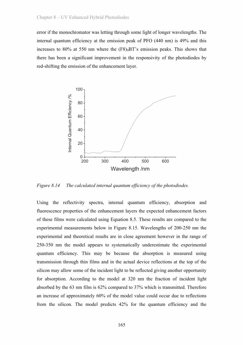
Chapter 8 – UV Enhanced Hybrid Photodiodes
165
error if the monochromator was letting through some light of longer wavelengths. The
internal quantum efficiency at the emission peak of PFO (440 nm) is 49% and this
increases to 80% at 550 nm where the (F8)9BT’s emission peaks. This shows that
there has been a significant improvement in the responsivity of the photodiodes by
red-shifting the emission of the enhancement layer.
200 300 400 500 6000
20
40
60
80
100
Inte
rna
l Q
ua
ntu
m E
ffic
ien
cy /
%
Wavelength /nm
Figure 8.14 The calculated internal quantum efficiency of the photodiodes.
Using the reflectivity spectra, internal quantum efficiency, absorption and
fluorescence properties of the enhancement layers the expected enhancement factors
of these films were calculated using Equation 8.5. These results are compared to the
experimental measurements below in Figure 8.15. Wavelengths of 200-250 nm the
experimental and theoretical results are in close agreement however in the range of
250-350 nm the model appears to systematically underestimate the experimental
quantum efficiency. This may be because the absorption is measured using
transmission through thin films and in the actual device reflections at the top of the
silicon may allow some of the incident light to be reflected giving another opportunity
for absorption. According to the model at 320 nm the fraction of incident light
absorbed by the 63 nm film is 62% compared to 37% which is transmitted. Therefore
an increase of approximately 60% of the model value could occur due to reflections
from the silicon. The model predicts 42% for the quantum efficiency and the
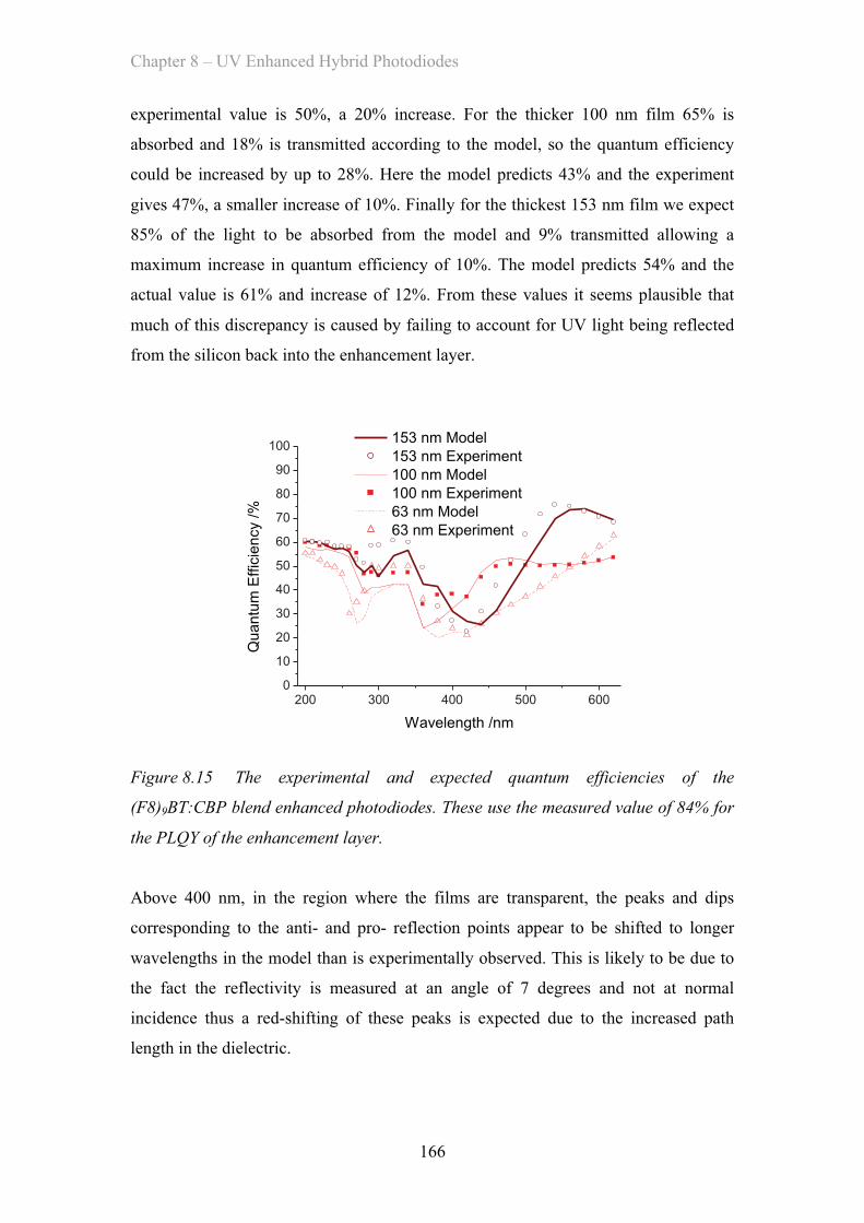
Chapter 8 – UV Enhanced Hybrid Photodiodes
166
experimental value is 50%, a 20% increase. For the thicker 100 nm film 65% is
absorbed and 18% is transmitted according to the model, so the quantum efficiency
could be increased by up to 28%. Here the model predicts 43% and the experiment
gives 47%, a smaller increase of 10%. Finally for the thickest 153 nm film we expect
85% of the light to be absorbed from the model and 9% transmitted allowing a
maximum increase in quantum efficiency of 10%. The model predicts 54% and the
actual value is 61% and increase of 12%. From these values it seems plausible that
much of this discrepancy is caused by failing to account for UV light being reflected
from the silicon back into the enhancement layer.
200 300 400 500 6000
10
20
30
40
50
60
70
80
90
100
Qu
an
tum
Eff
icie
ncy /
%
Wavelength /nm
153 nm Model
153 nm Experiment
100 nm Model
100 nm Experiment
63 nm Model
63 nm Experiment
Figure 8.15 The experimental and expected quantum efficiencies of the
(F8)9BT:CBP blend enhanced photodiodes. These use the measured value of 84% for
the PLQY of the enhancement layer.
Above 400 nm, in the region where the films are transparent, the peaks and dips
corresponding to the anti- and pro- reflection points appear to be shifted to longer
wavelengths in the model than is experimentally observed. This is likely to be due to
the fact the reflectivity is measured at an angle of 7 degrees and not at normal
incidence thus a red-shifting of these peaks is expected due to the increased path
length in the dielectric.
Chapter 8 – UV Enhanced Hybrid Photodiodes
167
A better calculation would measure or model reflectivity of the photodiodes at normal
incidence and possibly include a more reliable estimate of the amount of light
absorbed taking reflections at the silicon interface into account. Despite these issues
the model does a reasonable job of fitting the data. This shows that the simple
estimate of the coupling efficiency based on the refractive index of the enhancement
layer and the escape cone model of light out coupling, has generated results which are
consistent with experiment.
8.5 Conclusions
In this Chapter I have discussed the creation of hybrid organic-inorganic
photodetectors that use a highly emissive layer to down convert incident UV light to
wavelengths that can be detected by low cost silicon photodiodes. By making use of
energy transfer, I have used a high energy host and a longer wavelength emitting
guest. This gives good, even, UV absorption and long wavelength emission. This
~550 nm emission make use of the region where the silicon photodiodes have good
internal quantum efficiency. This has enabled the fabrication of devices with up to
61% quantum efficiency at 200 nm wavelength or 60-34% quantum efficiency over
the 200-620 nm wavelength range.
These results show that solution processed organic semiconductors can be used to
produce devices, that can match or beat the performance of lumogen based
commercial UV enhanced silicon CCDs. I have also shown that these performances
can be achieved using ~100 nm thick films that will be thin enough for multi-pixel
applications. By using solution processing, these devices will be easier to manufacture
than their thermally evaporated counterparts. In addition I have shown that the
performance of these devices can be estimated using a simple model using an escape
cone model for the fraction of light captured from the enhancement layer and coupled
into the silicon photodiode.
The blends of organic materials can easily be optimised both in terms of composition
and layer thickness to give absorption and thin film interference that are most suitable
for the wavelength range required for a given application. The current results and this
Chapter 8 – UV Enhanced Hybrid Photodiodes
168
flexibility mean that this work has applications in making higher sensitivity and lower
cost UV enhanced CCDs than are currently used commercially.
1. Jones, D.G., Photodiode Array Detectors in UV-Vis Spectroscopy. Part 1. Analytical Chemistry, 1985. 57(9): p. 1057-&.
2. Joseph, C.L., Advances in astronomical UV image sensors and associated technologies, in Photodetectors: Materials and Devices Ii, G.J. Brown and M. Razeghi, Editors. 1997. p. 244-258.
3. Soukhanovskii, V.A., et al., Compact collimated vacuum ultraviolet diagnostics for localized impurity measurements in fusion boundary plasmas. Review of Scientific Instruments, 2001. 72(8): p. 3270-3276.
4. Green, M.A. and M.J. Keevers, Optical-Properties of Intrinsic Silicon at 300 K. Progress in Photovoltaics, 1995. 3(3): p. 189-192.
5. Monroy, E., F. Omnes, and F. Calle, Wide-bandgap semiconductor ultraviolet photodetectors. Semiconductor Science and Technology, 2003. 18(4): p. R33-R51.
6. Su, Z.S., et al., High response organic ultraviolet photodetector based on blend of 4,4 ', 4 ''-tri-(2-methylphenyl phenylamino) triphenylaine and tris-(8-hydroxyquinoline) gallium. Applied Physics Letters, 2008. 93(10).
7. Lin, H.W., et al., Highly efficient visible-blind organic ultraviolet photodetectors. Advanced Materials, 2005. 17(20): p. 2489-+.
8. Ray, D. and K.L. Narasimhan, High response organic visible-blind ultraviolet detector. Applied Physics Letters, 2007. 91(9).
9. Forrest, S.R., The path to ubiquitous and low-cost organic electronic appliances on plastic. Nature, 2004. 428: p. 911.
10. Yang, Y., G.A. Turnbull, and I.D.W. Samuel, Hybrid optoelectronics: A polymer laser pumped by a nitride light-emitting diode. Applied Physics Letters, 2008. 92(16): p. 163306.
11. Garbuzov, D.Z., et al., Organic films deposited on Si p-n junctions: Accurate measurements of fluorescence internal efficiency, and application to luminescent antireflection coatings. Journal of Applied Physics, 1996. 80(8): p. 4644-4648.
12. Blouke, M.M., et al., Ultraviolet Downconverting Phosphor for Use With Silicon CCD Imagers. Applied Optics, 1980. 19(19): p. 3318-3321.
13. Kristianpoller, N. and D. Dutton, Optical Properties of "Liumogen": A Phosphor for Wavelength Conversion. Applied Optics, 1964. 3(2): p. 287.
14. Cowens, M.W., et al., Coronene and Liumogen as VUV Sensitive Coatings for Si CCD Imagers - A Comparison. Applied Optics, 1980. 19(22): p. 3727-3728.
15. Vardeny, Z.V., S.A. Jeglinski, and P.A. Lane, Enhanced Radiation Detectors Using Luminescent Materials. United States Department of Energy, 2001(US Patent Application 6211524 B1).
16. Ranger, M., D. Rondeau, and M. Leclerc, New well-defined poly(2,7-fluorene) derivatives: Photoluminescence and base doping. Macromolecules, 1997. 30(25): p. 7686-7691.
17. Bradley, D.D.C., et al., Influence of aggregation on the optical properties of a polyfluorene, in Optical Probes of Conjugated Polymers, Z.V. Vardeny and L.J. Rothberg, Editors. 1997. p. 254-259.
18. Redecker, M., et al., Nondispersive hole transport in an electroluminescent polyfluorene. Applied Physics Letters, 1998. 73(11): p. 1565-1567.
Chapter 8 – UV Enhanced Hybrid Photodiodes
169
19. Stevens, M.A., et al., Exciton dissociation mechanisms in the polymeric semiconductors poly(9,9-dioctylfluorene) and poly(9, 9-dioctylfluorene-co-benzothiadiazole). Physical Review B, 2001. 63(16).
20. Amarasinghe, D., et al., High-Gain Broadband Solid-State Optical Amplifier using a Semiconducting Copolymer. Advanced Materials, 2009. 21(1): p. 107-110.
21. Greenham, N.C., et al., Measurement of Absolute Photoluminescence Quantum Efficiencies in Conjugated Polymers. Chemical Physics Letters, 1995. 241(1-2): p. 89-96.
22. Garnir, H.P. and P.H. Lefebvre, Quantum efficiency of back-illuminated CCD detectors in the VUV region (30-200 nm). Nuclear Instruments & Methods in Physics Research Section B-Beam Interactions with Materials and Atoms, 2005. 235: p. 530-534.
23. Liu, Z.T., et al., The characterization of the optical functions of BCP and CBP thin films by spectroscopic ellipsometry. Synthetic Metals, 2005. 150(2): p. 159-163.
170
9. Conclusion
One of the many useful applications of semiconductor materials is optoelectronics, the
science of inter-converting light and electricity. Examples of these devices include
LEDs, solar cells, CCD cameras and compact solid state lasers. This thesis has
focused on the photophysics and applications of light emitting organic
semiconductors, with a particular emphasis on light emitting diodes.
Organic semiconductors are made from conjugated carbon based systems and through
organic chemistry many possible molecular structures can be synthesised and
investigated. This allows the materials properties to be easily tuned for specific
applications. One important issue with organic semiconductors is that they can suffer
from concentration quenching of their luminescence, and this can be a particular
problem in the solid state. This can reduce the efficiency of light emitting devices and
so it is important to control it. In this thesis I have investigated materials which use a
number of different strategies for controlling concentration quenching: in Chapter 5
by twisting molecules to prevent π stacking, in Chapter 6 by using bulky dendrons to
sterically protect emissive cores [1] and in Chapter 7 by using high energy spacer
units to prevent aggregation along a polymer chain. Another strategy is host-guest
blending which separates the chromophores in a higher energy host which can be
optimised for charge transport. This approach is used to augment the dendrimer
materials in Chapters 6 and 7 and is also used in Chapter 8 to increase the coverage of
the absorption spectrum of the enhancement layers.
In addition organic materials can be made soluble and are generally amorphous which
makes low cost solution processing of devices on rigid or flexible substrates [2]. The
ability to deposit devices on large areas at low cost makes these materials suitable for
large area solar cells and low glare lighting installations. If the solution properties of
these materials can be sufficiently controlled they can be deposited via ink-jet printing
allowing the printing of transistors for processing [3] or light emitting diodes for
displays [4]. Chapters 6 and 7 covered the development of high efficiency emissive
layers for ink-jet printable OLEDs by polymerising successful dendrimer materials so
that higher viscosity solutions, suitable for printing, could be achieved. Taking
Chapter 9 – Conclusion
171
advantage of the ease of deposition via solution processing is also part of the theme of
Chapter 8, where I have shown how an efficient UV enhancement layer can be spin
coated onto silicon photodiodes.
In Chapter 5 I showed how a planar molecule (triphenylene) could be prone to π-
stacking, leading to red-shifted emission in the solid state and multiple emissive
lifetimes in the time-resolved luminescence. By adding extra methyl groups the
hexamethyltriphenylene (HMTP) molecule was twisted out of one plane due to steric
crowding [5]. This prevented both the concentration dependent red-shifting of the
emission spectrum in solution and made sure there was only one emissive state. I also
showed how the strength of the optical transitions of molecules can be affected by
changing their shape. Triphenylene has a symmetry that makes the S0 to S1 transition
rather weak [6-8] and by changing the shape of the molecule this increased both the
absorption and emission dipole moments from 0.7 D to 3.6 D and 0.5 D to 2.1 D
respectively. This resulted in a ~20 times increase in the radiative de-excitation rate,
and taken with the reduced aggregation effects this meant that HMTP became a
moderately efficient emitter in the solid state with a photoluminescence quantum yield
(PLQY) of 31%.
Futher work in this area would investigate the reasons why HMTP has higher film
PLQY (31%) than solution (5%) and the possible existence of dark conformers related
to the interconversion of the molecules between different conformers. This might be
best investigated by freezing out these interconversions and performing photophysical
measurements of absolute quantum yield and time resolved luminescence at low
temperature. These measurements are challenging because many solvents can freeze
and become scattering at low temperatures. Methyl THF was considered as a
candidate for these measurements it forms a transparent glass however it or dissolved
impurities were found to react chemically with the HMTP. A further problem with
these measurement is a relative method of PLQY measurement cannot be used if there
is significant thermal expansion or contraction of the solvent.
Chapters 6 & 7 focused on Iridium based phosphorescent materials for OLEDs.
Phosphorescent materials are necessary for achieving the highest efficiencies in
Chapter 9 – Conclusion
172
electroluminescence because they can emit from triplet excited states, a large number
of which are formed under electrical excitation. In contrast organic materials they do
not include heavy metal atoms are fluorescent and cannot harvest these triplet states
[9].
Unlike dendrimers, which have previously be used to produce successful solution
processable phosphorescent OLEDs with up to 16% external quantum efficiency [10],
in this case the materials investigated were phosphorescent polymers. The aim of this
work was to increase the viscosity of solution so that phosphorescent devices might be
fabricated with ink-jet printing. Many previous attempts used phosphorescent
polymers with conjugated backbones, however these sometimes accepted back
transfer of the triplet states which then became trapped on the fluorescent backbone
and were thus lost [11]. In this work a non-conjugated backbone was used to prevent
quenching via back transfer of triplets. The pendant iridium complexes made use of
dendrons to reduce intermolecular interactions. By using double dendrons structures
with two dendrons per ligand interactions were further reduced. For the
homopolymers investigated in Chapter 6, this allowed the production of OLEDs with
9.3% external quantum efficiency. With host guest blending using CBP as a charge
transport host the efficiency was increased to 12.1%.
One issue with phosphorescent homopolymers with pedant iridium complexes is that
the emissive cores are not sufficiently separated along the chain of the polymer to
prevent intra chain concentration quenching. This results in some quenching of the
luminescence of the polymers even in dilute solutions. This can be detected from both
a reduction in the PLQY values and from non-exponential time-resolved
luminescence characteristics indicating there is more than one emissive state. While
the monomer’s of the more emissive 2-phenylpydridyl (ppy)/phenyltriazolyl (ptz)
based materials achieved >90% PLQY in solution these interactions limited the
solution PLQY of the homopolymers discussed in Chapter 6 to 61-67%.
In Chapter 7 I investigated the use of co-polymers with high energy gap spacer units
to reduce interchormophore interactions along the polymer chain. By using high
energy poly(styrene) spacer groups the solution PLQY was increased to 94% and
mono-exponential luminescence decay was achieved indicating that intra-molecular
Chapter 9 – Conclusion
173
interactions had been eliminated in solution. When blended with the charge transport
host CBP this allowed 6.7% EQE OLEDs to be produced. However, the high energy
of the poly(styrene) spacer units meant they would not contribute to charge transport
and this is undesirable in a material intended for use in OLEDs.
Materials with charge transporting, poly(9-vinylcarbazole) (PVK), spacer units were
investigated next with the aim of retaining the desirable photophysics of the
poly(styrene) co-polymer while improving charge transport. Although these materials
did show only one emissive state in time resolved luminescence the PLQY values
were reduced to 64-69% compared to >90% for the emissive monomers. This may
have been due to back transfer of triplet excitons from the iridium complexes onto the
PVK spacer units. Nevertheless these co-polymers resulted in efficient neat devices
with 10-11 % EQE. The best device achieved 14.7% EQE on blending with CBP,
which is higher than previous reports for a phosphorescent polymer of 11.8% EQE
[12].
Photophysical investigation could determine of the solid state PLQY of these
materials was indeed being reduced by back transfer to the PVK units and offer a
route to still more efficient materials for devices. Futher optimisation of the OLEDs to
achiever lower drive voltages and higher power efficiencies would be desirable. This
would involve adjusting layer thicknesses, considering alternative charge transport
hosts and possibly improving hole injection by using a PEDOT:PSS layer on the
anode. Ideally the charge balance would be optimised by adjusting the transport
groups in the co-polymer structure or by adding charge transport dendrons [13].
Optimising the OLED structure would be easier if the carrier transport of the
polymers and co-polymers was characterised, perhaps by the time of flight or single
carrier device methods, and it would be interesting to see if the charge transport
properties were significantly different from in comparable dendrimer films.
The high luminescence efficiency and easy processing of organic semiconductors
were used to good effect in Chapter 8 to enhance the UV response of a silicon
photodiodes. As silicon photodiodes do not show much response to UV light but are
sensitive to longer wavelengths, a luminescent layer was added to the top of the
devices to downcovert the energy of incident light. By using a blend of a long
Chapter 9 – Conclusion
174
wavelength emitting polymer with a higher energy host efficient absorption in the UV
was combined with re-emission at wavelengths were the silicon photodiode was most
sensitive achieving 61% external quantum efficiency. The strong absorbance of the
enhancement layers allowed thin ~100 nm films to be used which would be thin
enough to be used for enhancement of multipixel detectors like CCDs without
introducing cross talk between pixels. This is promising because it shows an
efficiency significantly better than 20-30% EQE reported for currently used lumogen
devices [14, 15], but also it can be solution processed, rather than the normally
deposited via thermal evaporation in high vacuum normally used for lumogen.
The next step for this project would be the enhancement of a CCD device and to
determined the effects of the enhancement layer on pixel cross talk. Further
optimisation of this enhancement layer would also be possible by varying materials,
blend ratios and layer thicknesses. Although these devices were shown to be stable in
air, their lifetime would need to be investigated and controlled under operating
conditions. This would possibly involve making use of UV transparent thin film
encapsulation.
Emissive organic light emitting diode displays are already being deployed
commercially and in the future solution processable OLEDs, possibly on flexible
substrates, may provide low cost, energy efficient portable device displays and large
area low-glare lighting and signage [2]. This thesis has contributed to the investigation
of high efficiency phosphorescent materials available for solution processed OLEDs.
By combing the strengths of organics with inorganics hybrid devices allow us make
use of the best of both systems. For example using organic layers as light
concentrators for high performance but expensive inorganic solar cells [16] or making
compact LED pumped tuneable polymer lasers [17]. In this work I have shown that
solution processed organics are versatile and efficient materials for making hybrid UV
photodetectors. Taking all of this into account, the future of organic optoelectronics
looks bright indeed.
1. Burn, P.L., S.C. Lo, and I.D.W. Samuel, The development of light-emitting dendrimers for displays. Advanced Materials, 2007. 19(13): p. 1675-1688.
2. Forrest, S.R., The path to ubiquitous and low-cost organic electronic appliances on plastic. Nature, 2004. 428: p. 911.
Chapter 9 – Conclusion
175
3. Yan, H., et al., A high-mobility electron-transporting polymer for printed transistors. Nature, 2009. 457(7230): p. 679.
4. Shimoda, T., et al., Inkjet printing of light-emitting polymer displays. Mrs Bulletin, 2003. 28(11): p. 821-827.
5. Wang, Y., et al., 1,4,5,8,9,12-hexamethyltriphenylene. A molecule with a flipping twist. Journal of the American Chemical Society, 2007. 129(43): p. 13193-13200.
6. Markovitsi, D., et al., Triphenylene Columnar Liquid-Crystals - Excited States and Energy Transfer. Journal of Physical Chemistry, 1995. 99(3): p. 1005-1017.
7. Di Donato, E., et al., Tuning Fluorescence Lifetimes through Changes in Herzberg-Teller Activities: The Case of Triphenylene and Its Hexamethoxy-Substituted Derivative. Journal of Physical Chemistry A, 2009. 113(23): p. 6504-6510.
8. Kokkin, D.L., et al., Gas phase spectra of all-benzenoid polycyclic aromatic hydrocarbons: Triphenylene. Journal of Chemical Physics, 2007. 126(8).
9. Baldo, M.A., et al., Highly efficient phosphorescent emission from organic electroluminescent devices. Nature, 1998. 395(6698): p. 151-154.
10. Lo, S.C., et al., Green phosphorescent dendrimer for light-emitting diodes. Advanced Materials, 2002. 14(13-14): p. 975.
11. Sudhakar, M., et al., Phosphorescence quenching by conjugated polymers. Journal of the American Chemical Society, 2003. 125(26): p. 7796-7797.
12. Suzuki, M., et al., Highly efficient polymer light-emitting devices using ambipolar phosphorescent polymers. Applied Physics Letters, 2005. 86(10): p. 103507.
13. Gambino, S., et al., Control of Charge Transport in Iridium(III) Complex-Cored Carbazole Dendrimers by Generation and Structural Modification. Advanced Functional Materials, 2009. 19(2): p. 317-323.
14. Blouke, M.M., et al., Ultraviolet Downconverting Phosphor for Use With Silicon CCD Imagers. Applied Optics, 1980. 19(19): p. 3318-3321.
15. Garnir, H.P. and P.H. Lefebvre, Quantum efficiency of back-illuminated CCD detectors in the VUV region (30-200 nm). Nuclear Instruments & Methods in Physics Research Section B-Beam Interactions with Materials and Atoms, 2005. 235: p. 530-534.
16. Currie, M.J., et al., High-efficiency organic solar concentrators for photovoltaics. Science, 2008. 321(5886): p. 226-228.
17. Yang, Y., G.A. Turnbull, and I.D.W. Samuel, Hybrid optoelectronics: A polymer laser pumped by a nitride light-emitting diode. Applied Physics Letters, 2008. 92(16): p. 163306.
176
Appendix: Publications
Chapter 5: Fluorescent Enhancement Using a Twisted Tripheneylene
Derivative
J. W. Levell, A. Ruseckas, J. B. Henry, Y. Wang, A. D. Stretton, A. R. Mount, T. H.
Galow, I. D. W. Samuel, Fluorescence Enhancement by Symmetry Breaking in a
Twisted Triphenylene Derivative. Journal of Physical Chemistry A, 2010. 114(51): p.
13291.
Chapter 6: Poly(dendrimer) Iridium Complexes
Lai, W.Y., et al., A study on the preparation and photophysical properties of an
iridium(III) complexed homopolymer. Journal of Materials Chemistry, 2009. 19(28):
p. 4952-4959.
W. Y. Lai, J. W. Levell, A. C. Jackson, S. C. Lo, P. V. Bernhardt, I. D. W. Samuel, P.
L. Burn, A Phosphorescent Poly(dendrimer) Containing Iridium(III) Complexes:
Synthesis and Light-Emitting Properties. Macromolecules, 2010. 43(17): p. 6986-
6994.
W. Y. Lai, J. W. Levell, S. C. Lo, P. L. Burn, and I. D. W. Samuel, The ‘Double
Dendron’ Approach to Host Free Phosphorescent Poly(dendrimer)
OLEDs. Advanced Materials, 2011. Submitted
Related Work:
J. P. Gunning, J. W. Levell, M. F. Wyatt, P. L. Burn, J. Robertson, I. D. W. Samuel,
The development of poly(dendrimer)s for advanced processing. Polymer Chemistry,
2010. 1(5): p. 730-738.
Appendix: Publications
177
J. W. Levell, J. P. Gunning, P. L. Burn, J. Robertson, I. D. W. Samuel, A
phosphorescent poly(dendrimer) with increased viscosity for solution-processed
OLED devices Organic Electronics, 2010. 11(9): p. 1561-1568
Conference Proceedings:
J. P. Gunning, K. A. Knights, J. C. Ribierre, R. E. Harding, J. W. Levell, P. L. Burn, I.
D. W. Samuel, Light-emitting poly(dendrimer)s - art. no. 70511X. Proceedings of the
SPIE, 2008. 7051: p. X511-X511.
J. W. Levell, W. Y. Lai, S. C. Lo, P. L. Burn and I. D. W. Samuel, Iridium (III)
Complex-based Small Molecules, Dendrimers and Poly(dendrimers) for Organic
Light-Emitting Diodes, Polymer Preprints, 2011. Submitted
Chapter 7: Phosphorescent Copolymer Dendrimers
J. W. Levell, W. Y. Lai, R. J. Borthwick, S. C. Lo, P. L. Burn and I. D. W. Samuel,
Efficient phosphorescence by reducing intrachain chromophore interactions in
dendrimer containing polymers, Journal of Physical Chemistry C, 2011. Submitted
J. W. Levell, W. Y. Lai, S. C. Lo, P. L. Burn and I. D. W. Samuel, Carbazoyl /iridium
dendrimer based phosphorescent copolymers for efficient light emitting devices, New
Journal of Chemistry, In Preparation
Chapter 8: UV Enhanced Hybrid Photodiodes
Levell, J.W., M.E. Giardini, and I.D.W. Samuel, A hybrid organic
semiconductor/silicon photodiode for efficient ultraviolet photodetection. Optics
Express, 2010. 18(4): p. 3219-3225.
Appendix: Publications
178
Other Publications
G. C. Fortman, A. Poater, J. W. Levell, S. Gaillard, A. M. Z. Slawin, I. D. W. Samuel,
L. Cavallo, S. P. Nolan, A versatile gold synthon for acetylene C-H bond activation.
Dalton Transactions, 2010. 39(43): p. 10382-10390.