California Volunteer Matching Network Overview CaliforniaVolunteers
QPD1003 500W, 50V, 1.2 – 1.4 GHz, GaN RF IMFET
Datasheet Rev. E, June 14, 2019 | Subject to change without notice - 1 of 18 - www.qorvo.com
Key Features • Frequency: 1.2 to 1.4 GHz
• Output Power (P3dB)1: 540 W
• Linear Gain1: 19.9 dB
• Typical PAE3dB1: 66.7%
• Operating Voltage: 50 V
• Low thermal resistance package
• Pulse capable
Note 1: @ 1.3 GHz
Product Overview The QPD1003 is a 500 W (P3dB) internally matched discrete
GaN on SiC HEMT which operates from 1.2 to 1.4 GHz and
a 50V supply rail. The device is GaN IMFET fully matched
to 50 Ω in an industry standard air cavity package and is
ideally suited for military and civilian radar. The device can
support pulsed and linear operations.
ROHS compliant.
Evaluation boards are available upon request.
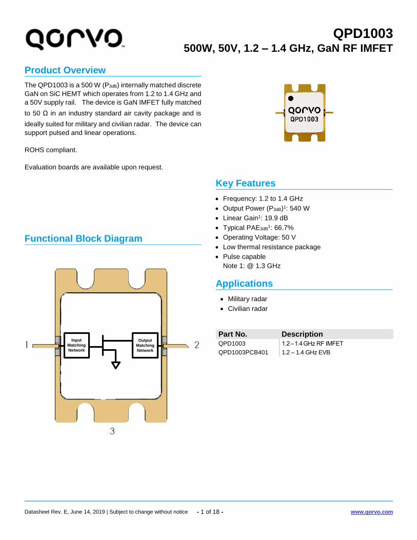
Functional Block Diagram
Applications • Military radar
• Civilian radar
Part No. Description
QPD1003 1.2 – 1.4 GHz RF IMFET
QPD1003PCB401 1.2 – 1.4 GHz EVB
Input
Matching
Network
Output
Matching
Network

QPD1003 500W, 50V, 1.2 – 1.4 GHz, GaN RF IMFET
Datasheet Rev. E, June 14, 2019 | Subject to change without notice - 2 of 18 - www.qorvo.com
Absolute Maximum Ratings1 Parameter Rating Units
Breakdown Voltage,BVDG +145 V
Gate Voltage Range, VG -7 to +2 V
Drain Current, IDMAX 20 A
Gate Current Range, IG See page 4. mA
Power Dissipation, 10% DC 1 mS PW, PDISS
410 W
RF Input Power, 10% DC 1 mS PW, 1.3 GHz, T = 25 °C
+42 dBm
Mounting Temperature (30 Seconds)
320 °C
Storage Temperature −65 to +150 °C
Notes:
1. Operation of this device outside the parameter ranges given above may cause permanent damage.
Recommended Operating Conditions1 Parameter Min Typ Max Units
Operating Temp. Range −40 +25 +85 °C
Drain Voltage Range, VD +28 +50 +55 V
Drain Bias Current, IDQ – 750 – mA
Drain Current, ID – 15 – A
Gate Voltage, VG4 – −2.8 – V
Power Dissipation, Pulsed (PD)2, 3
– – 370 W
Notes: 1. Electrical performance is measured under conditions noted
in the electrical specifications table. Specifications are not guaranteed over all recommended operating conditions.
2. Package base at 85 °C
3. Pulse Width = 1 mS, Duty Cycle = 10%
4. To be adjusted to desired IDQ
Pulsed Characterization – Load-Pull Performance – Power Tuned1 Parameters Typical Values Unit
Frequency, F 1.2 1.3 1.4 GHz
Linear Gain, GLIN 19 19.9 18.6 dB
Output Power at 3dB compression point, P3dB
57.3 57.3 57 dBm
Power-Added-Efficiency at 3dB compression point, PAE3dB
55.1 57.6 56.9 %
Gain at 3dB compression point 16 16.9 15.6 dB
Notes: 1. Test conditions unless otherwise noted: VD = +50 V, IDQ = 750 mA, Temp = +25 °C
Pulsed Characterization – Load-Pull Performance – Efficiency Tuned1 Parameters Typical Values Unit
Frequency, F 1.2 1.3 1.4 GHz
Linear Gain, GLIN 20.3 20.6 19.4 dB
Output Power at 3dB compression point, P3dB
55.4 55.6 55.3 dBm
Power-Added-Efficiency at 3dB compression point, PAE3dB
70.3 66.7 67.4 %
Gain at 3dB compression point, G3dB
17.3 17.6 16.4 dB
Notes: 1. Test conditions unless otherwise noted: VD = +50 V, IDQ = 750 mA, Temp = +25 °C

QPD1003 500W, 50V, 1.2 – 1.4 GHz, GaN RF IMFET
Datasheet Rev. E, June 14, 2019 | Subject to change without notice - 3 of 18 - www.qorvo.com
RF Characterization – 1.2 – 1.4 GHz EVB Performance At 1.2 GHz1 Parameter Min Typ Max Units
Linear Gain, GLIN – 18.6 – dB
Output Power at 3dB compression point, P3dB – 57.1 – dBm
Power-Added Efficiency at 3dB compression point, PAE3dB
– 57.7 – %
Gain at 3dB compression point, G3dB – 15.6 – dB
Notes: 1. VD = +50 V, IDQ = 750 mA, Temp = +25 °C, CW
RF Characterization – 1.2 – 1.4 GHz EVB Performance At 1.4 GHz1 Parameter Min Typ Max Units
Linear Gain, GLIN – 18.5 – dB
Output Power at 3dB compression point, P3dB – 56.4 – dBm
Power-Added Efficiency at 3dB compression point, PAE3dB
– 59.2 – %
Gain at 3dB compression point, G3dB – 15.5 – dB
Notes: 1. VD = +50 V, IDQ = 750 mA, Temp = +25 °C, CW
RF Characterization – Mismatch Ruggedness at 1.3 GHz1 Symbol Parameter dB Compression Typical
VSWR Impedance Mismatch Ruggedness 3 5:1
Notes: 1. Test conditions unless otherwise noted: TA = 25 °C, VD = 50 V, IDQ = 750 mA, 1 mS PW, 10% DC 2. Driving input power is determined at pulsed compression under matched condition at EVB output connector.
RF Characterization – 1.2 – 1.4 GHz EVB Performance At 1.3 GHz1 Parameter Min Typ Max Units
Linear Gain, GLIN – 19.8 – dB
Output Power at 3dB compression point, P3dB – 56.6 – dBm
Power-Added Efficiency at 3dB compression point, PAE3dB
– 62.0 – %
Gain at 3dB compression point, G3dB – 16.8 – dB
Notes: 1. VD = +50 V, IDQ = 750 mA, Temp = +25 °C, CW
QPD1003 500W, 50V, 1.2 – 1.4 GHz, GaN RF IMFET
Datasheet Rev. E, June 14, 2019 | Subject to change without notice - 4 of 18 - www.qorvo.com
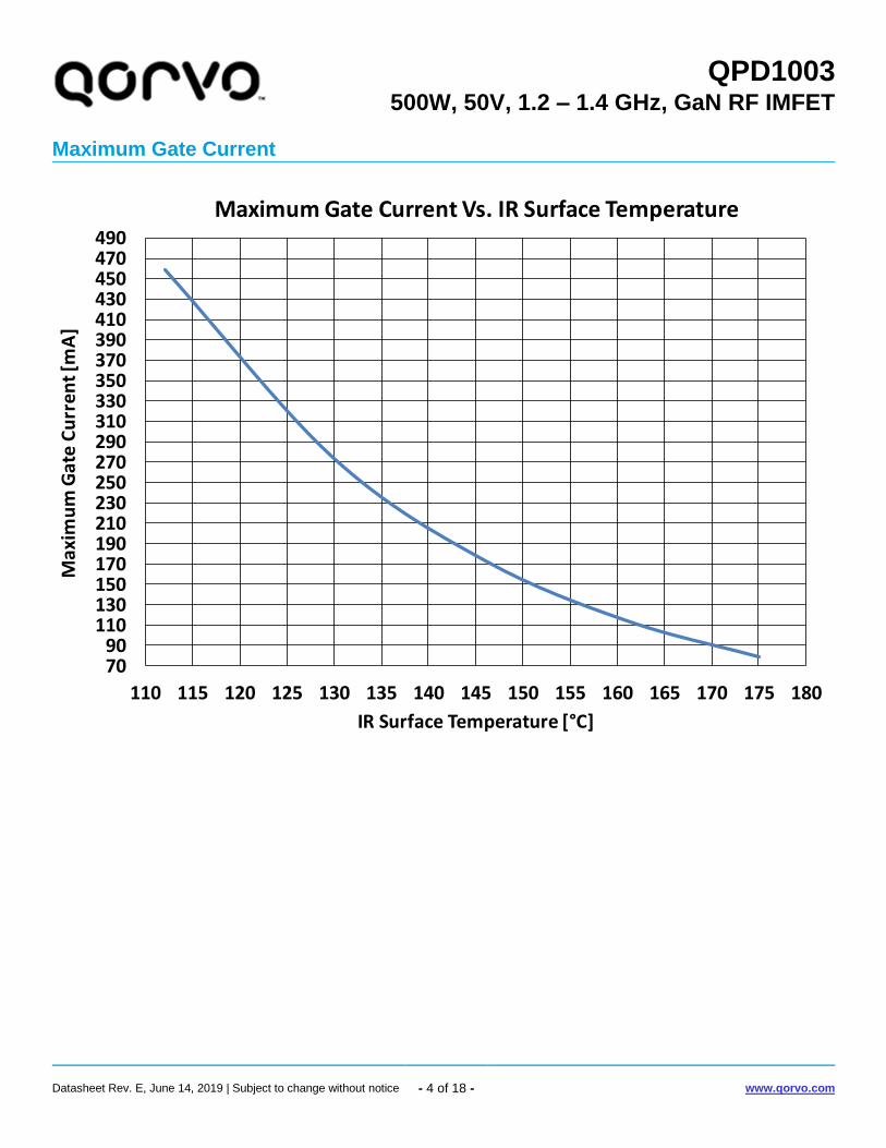
Maximum Gate Current
7090
110130150170190210230250270290310330350370390410430450470490
110 115 120 125 130 135 140 145 150 155 160 165 170 175 180
Max
imu
m G
ate
Cu
rren
t [m
A]
IR Surface Temperature [°C]
Maximum Gate Current Vs. IR Surface Temperature

QPD1003 500W, 50V, 1.2 – 1.4 GHz, GaN RF IMFET
Datasheet Rev. E, June 14, 2019 | Subject to change without notice - 5 of 18 - www.qorvo.com
1Refer to the following document GaN Device Channel Temperature, Thermal Resistance, and Reliability Estimates
Thermal and Reliability Information – Pulsed
Parameter Conditions Values Units Thermal Resistance, IR1 (θJC) 85 °C back side temperature
346 W Pdiss, 1 mS PW, 10% DC
0.30 °C/W
Peak IR Surface Temperature1 (TCH) 189 °C
40
60
80
100
120
140
160
180
200
220
240
260
280
300
320
1.0E-09 1.0E-07 1.0E-05 1.0E-03 1.0E-01
Peak I
R S
urf
ace T
em
pera
ture
[ C
]
Pulse Width [Sec]
Peak IR Surface Temperature vs. Pulse WidthPdiss = 346 W, Base Temperature @ 85 C

QPD1003 500W, 50V, 1.2 – 1.4 GHz, GaN RF IMFET
Datasheet Rev. E, June 14, 2019 | Subject to change without notice - 6 of 18 - www.qorvo.com
Load-Pull Smith Charts1, 2, 3 Notes:
1. VD = 50 V, IDQ = 750 mA, 1 mS PW, 10% DC pulsed. Performance is at 3dB gain compression referenced to peak gain.
2. See page 13 for load-pull and source-pull reference planes. 50-Ω load-pull TRL fixtures are built with 20-mil RO4350B material. 3. NaN means the impedances are either undefined or varying in load-pull system.
0.4
0.5
0.6
0.7
0.8
0.9
1 1.2
1.4
1.6
1.8
2 3
1.2GHz, Load-pull
57.2
57
56.8
17.4
16.9
16.4
68.5
66.564.5
• Max Power is 57.3dBm
at Z = 38.711+13.983i
= -0.0999+0.1734i
• Max Gain is 17.4dB
at Z = 146.401+21.891i
= 0.4971+0.0561i
• Max PAE is 70.3%
at Z = 117.619-0.032i
= 0.4034-0.0001i
Zo = 50
3dB Compression Referenced to Peak Gain
Zs(fo) = 50-0.01i
Zs(2fo) = 53.4+28.74i
Zs(3fo) = 67.51+56.9i
Zl(2fo) = NaN
Zl(3fo) = NaN
Power
Gain
PAE

QPD1003 500W, 50V, 1.2 – 1.4 GHz, GaN RF IMFET
Datasheet Rev. E, June 14, 2019 | Subject to change without notice - 7 of 18 - www.qorvo.com
Load-Pull Smith Charts1, 2, 3 Notes:
1. VD = 50 V, IDQ = 750 mA, 1 mS PW, 10% DC pulsed. Performance is at 3dB gain compression referenced to peak gain.
2. See page 13 for load-pull and source-pull reference planes. 50-Ω load-pull TRL fixtures are built with 20-mil RO4350B material. 3. NaN means the impedances are either undefined or varying in load-pull system.
0.5
0.6
0.7
0.8
0.9
1 1.2
1.4
1.6
1.8
2
1.3GHz, Load-pull
57.1 56.956.7
18
17.5
17
65.1
63.1
61.1
• Max Power is 57.3dBm
at Z = 33.332+0.002i
= -0.2
• Max Gain is 18.1dB
at Z = 37.815+48.733i
= 0.1294+0.4832i
• Max PAE is 66.7%
at Z = 63.965+19.872i
= 0.1484+0.1485i
Zo = 50
3dB Compression Referenced to Peak Gain
Zs(fo) = 49.99+0.01i
Zs(2fo) = 48.17+46.93i
Zs(3fo) = 39.12-47.6i
Zl(2fo) = NaN
Zl(3fo) = NaN
Power
Gain
PAE

QPD1003 500W, 50V, 1.2 – 1.4 GHz, GaN RF IMFET
Datasheet Rev. E, June 14, 2019 | Subject to change without notice - 8 of 18 - www.qorvo.com
Load-Pull Smith Charts1, 2, 3 Notes:
1. VD = 50 V, IDQ = 750 mA, 1 mS PW, 10% DC pulsed. Performance is at 3dB gain compression referenced to peak gain.
2. See page 13 for load-pull and source-pull reference planes. 50-Ω load-pull TRL fixtures are built with 20-mil RO4350B material. 3. NaN means the impedances are either undefined or varying in load-pull system.
0.7
0.8
0.9
1 1.2
1.4
1.6
1.8
2 3 4
1.4GHz, Load-pull
56.9 56.7
56.5
16
15.5
15
65.8
63.8
61.8
• Max Power is 57dBm
at Z = 46.156-19.245i
= 0.0001-0.2001i
• Max Gain is 16.5dB
at Z = 33.348+16.116i
= -0.1565+0.2236i
• Max PAE is 67.4%
at Z = 46.151+19.213i
= -0.0001+0.1998i
Zo = 50
3dB Compression Referenced to Peak Gain
Zs(fo) = 50-0.02i
Zs(2fo) = 43.81+72i
Zs(3fo) = 34.92-23.54i
Zl(2fo) = NaN
Zl(3fo) = NaN
Power
Gain
PAE

QPD1003 500W, 50V, 1.2 – 1.4 GHz, GaN RF IMFET
Datasheet Rev. E, June 14, 2019 | Subject to change without notice - 9 of 18 - www.qorvo.com
Typical Performance – Load-Pull Drive-up1, 2 Notes:
1. 1 mS PW, 10% DC pulsed signal, VD = 50 V, IDQ = 750 mA
2. See page 13 for load-pull and source-pull reference planes where the performance was measured.
46 47 48 49 50 51 52 53 54 55 56 57 5812
13
14
15
16
17
18
19
20
21
22
Output Power [dBm]
Ga
in [d
B]
QPD1003 - Gain and PAE vs. Output Power1.2 GHz - Power Tuned
Zs-fo = 50-0.01i
Zs-2fo = 53.4+28.74i
Zs-3fo = 67.51+56.9i
Zl-fo = 38.711+13.983i
Zl-2fo = NaN
Zl-3fo = NaN
46 47 48 49 50 51 52 53 54 55 56 57 5810
15
20
25
30
35
40
45
50
55
60
PA
E [%
]
Gain
PAE
46 47 48 49 50 51 52 53 54 55 5612
13
14
15
16
17
18
19
20
21
22
Output Power [dBm]
Ga
in [d
B]
QPD1003 - Gain and PAE vs. Output Power1.2 GHz - Efficiency Tuned
Zs-fo = 50-0.01i
Zs-2fo = 53.4+28.74i
Zs-3fo = 67.51+56.9i
Zl-fo = 117.619-0.032i
Zl-2fo = NaN
Zl-3fo = NaN
46 47 48 49 50 51 52 53 54 55 5625
30
35
40
45
50
55
60
65
70
75
PA
E [%
]
Gain
PAE
46 47 48 49 50 51 52 53 54 55 56 57 5812
13
14
15
16
17
18
19
20
21
22
Output Power [dBm]
Ga
in [d
B]
QPD1003 - Gain and PAE vs. Output Power1.3 GHz - Power Tuned
Zs-fo = 49.99+0.01i
Zs-2fo = 48.17+46.93i
Zs-3fo = 39.12-47.6i
Zl-fo = 33.332+0.002i
Zl-2fo = NaN
Zl-3fo = NaN
46 47 48 49 50 51 52 53 54 55 56 57 5810
15
20
25
30
35
40
45
50
55
60
PA
E [%
]
Gain
PAE
46 47 48 49 50 51 52 53 54 55 5612
13
14
15
16
17
18
19
20
21
22
Output Power [dBm]
Ga
in [d
B]
QPD1003 - Gain and PAE vs. Output Power1.3 GHz - Efficiency Tuned
Zs-fo = 49.99+0.01i
Zs-2fo = 48.17+46.93i
Zs-3fo = 39.12-47.6i
Zl-fo = 63.965+19.872i
Zl-2fo = NaN
Zl-3fo = NaN
46 47 48 49 50 51 52 53 54 55 5620
25
30
35
40
45
50
55
60
65
70
PA
E [%
]Gain
PAE

QPD1003 500W, 50V, 1.2 – 1.4 GHz, GaN RF IMFET
Datasheet Rev. E, June 14, 2019 | Subject to change without notice - 10 of 18 - www.qorvo.com
Typical Performance – Load-Pull Drive-up1, 2 Notes:
1. 1 mS PW, 10% DC pulsed signal, VD = 50 V, IDQ = 750 mA
2. See page 13 for load-pull and source-pull reference planes where the performance was measured.
46 47 48 49 50 51 52 53 54 55 56 57 5812
13
14
15
16
17
18
19
20
21
22
Output Power [dBm]
Ga
in [d
B]
QPD1003 - Gain and PAE vs. Output Power1.4 GHz - Power Tuned
Zs-fo = 50-0.02i
Zs-2fo = 43.81+72i
Zs-3fo = 34.92-23.54i
Zl-fo = 46.156-19.245i
Zl-2fo = NaN
Zl-3fo = NaN
46 47 48 49 50 51 52 53 54 55 56 57 5810
15
20
25
30
35
40
45
50
55
60
PA
E [%
]
Gain
PAE
46 47 48 49 50 51 52 53 54 55 5612
13
14
15
16
17
18
19
20
21
22
Output Power [dBm]
Ga
in [d
B]
QPD1003 - Gain and PAE vs. Output Power1.4 GHz - Efficiency Tuned
Zs-fo = 50-0.02i
Zs-2fo = 43.81+72i
Zs-3fo = 34.92-23.54i
Zl-fo = 46.151+19.213i
Zl-2fo = NaN
Zl-3fo = NaN
46 47 48 49 50 51 52 53 54 55 5620
25
30
35
40
45
50
55
60
65
70
PA
E [%
]
Gain
PAE

QPD1003 500W, 50V, 1.2 – 1.4 GHz, GaN RF IMFET
Datasheet Rev. E, June 14, 2019 | Subject to change without notice - 11 of 18 - www.qorvo.com
Power Drive-up Performance Over Temperatures Of 1.2 – 1.4 GHz EVB1
Notes:
1. VD = 50 V, IDQ = 750 mA, 1 mS PW, 10% DC
300
350
400
450
500
550
600
-40 -30 -20 -10 0 10 20 30 40 50 60 70 80 90
P3
dB
[W
]
Temperature [°C]
P3dB vs. Temperatures
1.2 GHz
1.3 GHz
1.4 GHz
10
11
12
13
14
15
16
17
18
19
20
-40 -30 -20 -10 0 10 20 30 40 50 60 70 80 90
G3
dB
[d
B]
Temperature [°C]
G3dB vs. Temperatures
1.2 GHz
1.3 GHz
1.4 GHz
40
45
50
55
60
65
70
75
80
-40 -30 -20 -10 0 10 20 30 40 50 60 70 80 90
DE3
dB
[%
]
Temperature [°C]
Drain Efficiency @ 3dB Compression vs. Temperatures
1.2 GHz
1.3 GHz
1.4 GHz
150
200
250
300
350
400
450
-40 -30 -20 -10 0 10 20 30 40 50 60 70 80 90
Pd
iss3
dB
[W
]
Temperature [°C]
Dissipation Power @ 3dB Compression vs. Temperatures
1.2 GHz
1.3 GHz
1.4 GHz
QPD1003 500W, 50V, 1.2 – 1.4 GHz, GaN RF IMFET
Datasheet Rev. E, June 14, 2019 | Subject to change without notice - 12 of 18 - www.qorvo.com
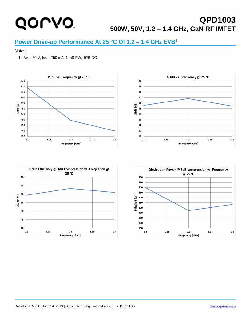
Power Drive-up Performance At 25 °C Of 1.2 – 1.4 GHz EVB1
Notes:
1. VD = 50 V, IDQ = 750 mA, 1 mS PW, 10% DC
430
440
450
460
470
480
490
500
510
520
530
1.2 1.25 1.3 1.35 1.4
P3
dB
[W
]
Frequency [GHz]
P3dB vs. Frequency @ 25 °C
10
11
12
13
14
15
16
17
18
19
20
1.2 1.25 1.3 1.35 1.4
G3
dB
[d
B]
Frequency [GHz]
G3dB vs. Frequency @ 25 °C
40
45
50
55
60
65
70
1.2 1.25 1.3 1.35 1.4
DE3
dB
[%
]
Frequency [GHz]
Drain Efficiency @ 3dB Compression vs. Frequency @ 25 °C
150
170
190
210
230
250
270
290
310
330
350
1.2 1.25 1.3 1.35 1.4
Pd
iss3
dB
[W
]
Frequency [GHz]
Dissipation Power @ 3dB compression vs. Frequency @ 25 °C
QPD1003 500W, 50V, 1.2 – 1.4 GHz, GaN RF IMFET
Datasheet Rev. E, June 14, 2019 | Subject to change without notice - 13 of 18 - www.qorvo.com
Notes:
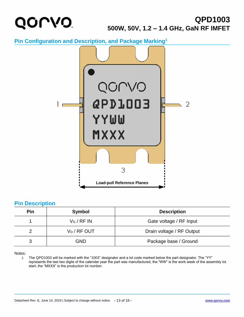
1. The QPD1003 will be marked with the “1003” designator and a lot code marked below the part designator. The “YY” represents the last two digits of the calendar year the part was manufactured, the “WW” is the work week of the assembly lot start, the “MXXX” is the production lot number.
Pin Configuration and Description, and Package Marking1
Pin Description
Pin Symbol Description
1 VG / RF IN Gate voltage / RF Input
2 VD / RF OUT Drain voltage / RF Output
3 GND Package base / Ground
Load-pull Reference Planes

QPD1003 500W, 50V, 1.2 – 1.4 GHz, GaN RF IMFET
Datasheet Rev. E, June 14, 2019 | Subject to change without notice - 14 of 18 - www.qorvo.com
Package Dimensions1, 2, 3
Notes: 1. Unless otherwise noted, the tolerance is ±0.15 mm. 2. For instruction to mount the part, please refer to application note “RF565 Package Mounting, Mechanical Mounting and PCB
Considerations.”

QPD1003 500W, 50V, 1.2 – 1.4 GHz, GaN RF IMFET
Datasheet Rev. E, June 14, 2019 | Subject to change without notice - 15 of 18 - www.qorvo.com
Schematic – 1.2 – 1.4 GHz EVB
Bias-up Procedure Bias-down Procedure
1. Set VG to -4 V. 1. Turn off RF signal.
2. Set ID current limit to 800 mA. 2. Turn off VD
3. Apply 50 V VD. 3. Wait 2 seconds to allow drain capacitor to discharge
4. Slowly adjust VG until ID is set to 750 mA. 4. Turn off VG
5. Set ID current limit to 2 A
6. Apply RF.
QPD1003 500W, 50V, 1.2 – 1.4 GHz, GaN RF IMFET
Datasheet Rev. E, June 14, 2019 | Subject to change without notice - 16 of 18 - www.qorvo.com
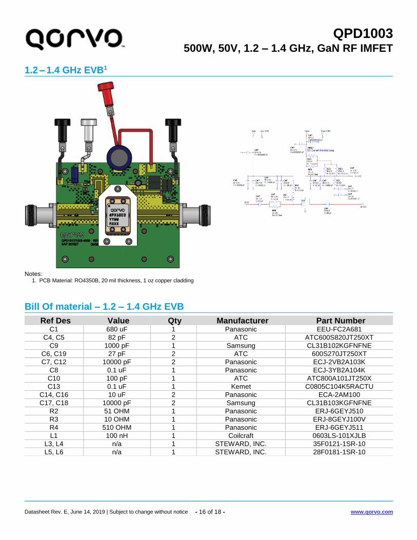
1.2 – 1.4 GHz EVB1
Notes: 1. PCB Material: RO4350B, 20 mil thickness, 1 oz copper cladding
Bill Of material – 1.2 – 1.4 GHz EVB
Ref Des Value Qty Manufacturer Part Number C1 680 uF 1 Panasonic EEU-FC2A681
C4, C5 82 pF 2 ATC ATC600S820JT250XT
C9 1000 pF 1 Samsung CL31B102KGFNFNE
C6, C19 27 pF 2 ATC 600S270JT250XT
C7, C12 10000 pF 2 Panasonic ECJ-2VB2A103K
C8 0.1 uF 1 Panasonic ECJ-3YB2A104K
C10 100 pF 1 ATC ATC800A101JT250X
C13 0.1 uF 1 Kemet C0805C104K5RACTU
C14, C16 10 uF 2 Panasonic ECA-2AM100
C17, C18 10000 pF 2 Samsung CL31B103KGFNFNE
R2 51 OHM 1 Panasonic ERJ-6GEYJ510
R3 10 OHM 1 Panasonic ERJ-8GEYJ100V
R4 510 OHM 1 Panasonic ERJ-6GEYJ511
L1 100 nH 1 Coilcraft 0603LS-101XJLB
L3, L4 n/a 1 STEWARD, INC. 35F0121-1SR-10
L5, L6 n/a 1 STEWARD, INC. 28F0181-1SR-10

QPD1003 500W, 50V, 1.2 – 1.4 GHz, GaN RF IMFET
Datasheet Rev. E, June 14, 2019 | Subject to change without notice - 17 of 18 - www.qorvo.com
Recommended Solder Temperature Profile

QPD1003 500W, 50V, 1.2 – 1.4 GHz, GaN RF IMFET
Datasheet Rev. E, June 14, 2019 | Subject to change without notice - 18 of 18 - www.qorvo.com
Handling Precautions Parameter Rating Standard
Caution! ESD-Sensitive Device
ESD – Human Body Model (HBM) Class 1B
950 V ANSI/ESD/JEDEC JS-001
ESD – Charged Device Model (CDM) Class C3
1000 V ANSI/ESD/JEDEC JS-002
MSL – Moisture Sensitivity Level MSL 3 IPC/JEDEC J-STD-020
Important Notice The information contained herein is believed to be reliable; however, Qorvo makes no warranties regarding the information contained herein and assumes no responsibility or liability whatsoever for the use of the information contained herein. All information contained herein is subject to change without notice. Customers should obtain and verify the latest relevant information before placing orders for Qorvo products. The information contained herein or any use of such information does not grant, explicitly or implicitly, to any party any patent rights, licenses, or any other intellectual property rights, whether with regard to such information itself or anything described by such information. THIS INFORMATION DOES NOT CONSTITUTE A WARRANTY WITH RESPECT TO THE PRODUCTS DESCRIBED HEREIN, AND QORVO HEREBY DISCLAIMS ANY AND ALL WARRANTIES WITH RESPECT TO SUCH PRODUCTS WHETHER EXPRESS OR IMPLIED BY LAW, COURSE OF DEALING, COURSE OF PERFORMANCE, USAGE OF TRADE OR OTHERWISE, INCLUDING THE IMPLIED WARRANTIES OF MERCHANTABILITY AND FITNESS FOR A PARTICULAR PURPOSE.
Without limiting the generality of the foregoing, Qorvo products are not warranted or authorized for use as critical components in medical, life-saving, or life-sustaining applications, or other applications where a failure would reasonably be expected to cause severe personal injury or death.
Copyright 2016 © Qorvo, Inc. | Qorvo is a registered trademark of Qorvo, Inc.
Contact Information For the latest specifications, additional product information, worldwide sales and distribution locations: Web: www.qorvo.com Tel: +1.844.890.8163 Email: [email protected] For technical questions and application information: Email: [email protected]
Solderability Compatible with both lead-free (260°C max. reflow temp.) and tin/lead (245°C max. reflow temp.) soldering processes.
Solder profiles available upon request.
Package lead plating is NiAu. Au thickness is 1.0 µm minimum.
RoHS Compliance This part is compliant with 2011/65/EU RoHS directive (Restrictions on the Use of Certain Hazardous Substances in Electrical and Electronic Equipment) as amended by Directive 2015/863/EU. This product also has the following attributes:
• Halogen Free (Chlorine, Bromine) • Antimony Free
• TBBP-A (C15H12Br402) Free
• PFOS Free
• SVHC Free

![Pyramid Stereo Matching Network · pyramid stereo matching network for depth estimation. 3. Pyramid Stereo Matching Network We present PSMNet, which consists of an SPP [9,32] module](https://static.fdocuments.in/doc/165x107/5f5ce14406f9f6678036ef57/pyramid-stereo-matching-network-pyramid-stereo-matching-network-for-depth-estimation.jpg)