Master theses CIC lter design with HLS - PoliTO
81
Politecnico di Torino Electronic engineering Master theses CIC filter design with HLS Master degree in Electronic Engineering Author: Simone Impagnatiello Supervisor: Prof. Mario Roberto Casu Co-supervisor: Prof. Luciano Lavagno
Transcript of Master theses CIC lter design with HLS - PoliTO

Politecnico di Torino
Electronic engineering
Master theses
CIC filter design with HLS
Master degree in Electronic Engineering
Author: Simone Impagnatiello
Supervisor: Prof. Mario Roberto Casu
Co-supervisor: Prof. Luciano Lavagno


Abstract
The thesis work is based on the use of the High-Level-Synthesis methodology and
focuses on the use of an High-Level-Synthesis tool, Mentor Catapult, to apply the HLS
design methodology to an industrial application. In collaboration with the company
Silicon Mitus, a CIC filter is developed. The CIC filter is one of the upstream filters in
an high-performance DAC for audio application, developed by Silicon Mitus. The thesis
goal is to prove that an architecture designed with HLS design methodology, can achieve
performance in terms of area, power consumption an timing, which are comparable with
the one obtained by an architecture, designed with the classical RTL design flow. The
thesis work starts with an introduction to HLS, explaining its concepts, the structures
of HLS tools and its advantages over those of RTL design flow. An overview on the
structures and the frequency behaviour of the CIC filters is reported, with different
CIC filter state-of-the-art architectural solutions. Finally the description of the design
flow is introduced and the final results are discussed.

Contents
Contents ii
List of Figures v
1 High-Level-Synthesis and Mentor Catapult 1
1.1 High-Level-Synthesis . . . . . . . . . . . . . . . . . . . . . . . . . . . . 1
1.1.1 Advantage of High-Level-Synthesis . . . . . . . . . . . . . . . . 2
1.1.2 HLS flow description . . . . . . . . . . . . . . . . . . . . . . . . 2
1.1.3 HLS State-Of-The-Art . . . . . . . . . . . . . . . . . . . . . . . 4
1.2 Catapult C . . . . . . . . . . . . . . . . . . . . . . . . . . . . . . . . . 5
1.2.1 Data types . . . . . . . . . . . . . . . . . . . . . . . . . . . . . . 6
1.2.2 Synthesis tool steps . . . . . . . . . . . . . . . . . . . . . . . . . 8
2 CIC filter and state of art 13
2.1 Cascaded Integrator and Comb (CIC) filter . . . . . . . . . . . . . . . . 13
2.2 CIC filter frequency response . . . . . . . . . . . . . . . . . . . . . . . 16
2.3 Two possible algorithms for a CIC filter implementation . . . . . . . . 19
2.4 State-of-the-art CIC filter . . . . . . . . . . . . . . . . . . . . . . . . . 21
2.4.1 Bit-serial implementation (Recursive structure) . . . . . . . . . 21
2.4.2 Implementation of a sharpened CIC filter . . . . . . . . . . . . . 23
2.4.3 CIC filter architecture with optimal performance . . . . . . . . 29
3 C++ algorithm 33
3.1 Reference filter specification . . . . . . . . . . . . . . . . . . . . . . . . 33
3.2 MATLAB code and algorithm by Silicon Mitus . . . . . . . . . . . . . 34
3.3 MATLAB code translated in C++ . . . . . . . . . . . . . . . . . . . . 37
i

CIC filter design with HLS ii
3.3.1 The testing environment in C++ . . . . . . . . . . . . . . . . . 37
3.3.2 Filter algorithm and its implementation . . . . . . . . . . . . . 39
3.4 C++ code to synthesize the CIC filter . . . . . . . . . . . . . . . . . . 43
4 CIC filter development with Catapult 50
4.1 Correctness verification of the synthesized architecture . . . . . . . . . 51
4.2 Different architectures of the CIC filter and Catapult results . . . . . . 53
4.3 Final architecture and optimizations . . . . . . . . . . . . . . . . . . . 55
4.3.1 Architecture functioning . . . . . . . . . . . . . . . . . . . . . . 61
5 Conclusion 65
A Code 67
A.1 Synthesizable code . . . . . . . . . . . . . . . . . . . . . . . . . . . . . 67
A.2 C++ Testbench . . . . . . . . . . . . . . . . . . . . . . . . . . . . . . . 69

List of Figures
1.1 HLS flow [1] . . . . . . . . . . . . . . . . . . . . . . . . . . . . . . . . . 3
1.2 Catapult flow . . . . . . . . . . . . . . . . . . . . . . . . . . . . . . . . 6
1.3 Quantization modes . . . . . . . . . . . . . . . . . . . . . . . . . . . . . 7
1.4 Overflow modes . . . . . . . . . . . . . . . . . . . . . . . . . . . . . . . 8
1.5 Methods for ac fixed . . . . . . . . . . . . . . . . . . . . . . . . . . . . 9
1.6 Operators for ac fixed . . . . . . . . . . . . . . . . . . . . . . . . . . . 10
1.7 SCVerify infrastructure . . . . . . . . . . . . . . . . . . . . . . . . . . . 12
2.1 Decimation filter with CIC structure . . . . . . . . . . . . . . . . . . . 14
2.2 A single integrator stage . . . . . . . . . . . . . . . . . . . . . . . . . . 14
2.3 A single differential stage, with M=1 . . . . . . . . . . . . . . . . . . . 15
2.4 Scheme of the CIC decimation filter structure . . . . . . . . . . . . . . 15
2.5 Decimation filter implemented as a cascade of FIR filters . . . . . . . . 16
2.6 CIC filter frequency response, with M=1 . . . . . . . . . . . . . . . . . 18
2.7 CIC filter frequency response with M=2 . . . . . . . . . . . . . . . . . 18
2.8 General structure of a recursive CIC filter 2.8 . . . . . . . . . . . . . . 19
2.9 General structure of a non-recursive CIC filter 2.8 . . . . . . . . . . . . 20
2.10 Comparison between non-recursive and recursive algorithm, in terms of
area, power consumption and frequency [8] . . . . . . . . . . . . . . . . 20
2.11 Structure of integrative stage (a) and derivative stage (b) [9] . . . . . . 22
2.12 Array registers and adder decoder [9] . . . . . . . . . . . . . . . . . . . 22
2.13 Stop-band attenuation of a 6 order CIC filters . . . . . . . . . . . . . . 23
2.14 Stop-band attenuation of a 8 order CIC filters . . . . . . . . . . . . . . 23
2.15 Stop-band attenuation of a 10 order CIC filters . . . . . . . . . . . . . 24
2.16 Pass-band droop of CIC filters of the 6-th order . . . . . . . . . . . . . 24
iii

CIC filter design with HLS iv
2.17 Pass-band droop of CIC filters of the 8-th order . . . . . . . . . . . . . 25
2.18 Pass-band droop of CIC filters of the 10-th order . . . . . . . . . . . . 25
2.19 The desired ACF curve that represents improvement in stop-band and
in pass-band . . . . . . . . . . . . . . . . . . . . . . . . . . . . . . . . . 26
2.20 Architecture of the sharpened-response CIC filter . . . . . . . . . . . . 27
2.21 Comparison between the standard CIC response and the sharpened CIC
response [12] . . . . . . . . . . . . . . . . . . . . . . . . . . . . . . . . . 27
2.22 CIC filter pass-band droop trend according to the decimation factors
and parametrized on the filter order [12] . . . . . . . . . . . . . . . . . 28
2.23 Sharpened CIC filter pass-band droop trend according to the decimation
factors and parametrized on the filter order [12] . . . . . . . . . . . . . 29
2.24 CIC filter for decimation operation [14] . . . . . . . . . . . . . . . . . . 30
2.25 Comparison of area between the optimized architecture and the one
produced by the MATLAB HDL code for ASIC implementation [14] . . 31
2.26 Comparison of power between the optimized architecture and the one
produced by the MATLAB HDL code for ASIC implementation [14] . . 31
2.27 Comparison of frequency between the optimized architecture and the
one produced by the MATLAB HDL code for ASIC implementation [14] 31
2.28 Comparison of area between the optimized architecture and the one
produced by the MATLAB HDL code for FPGA implementation [14] . 32
2.29 Comparison of frequency between the optimized architecture and the
one produced by the MATLAB HDL code for FPGA implementation [14] 32
3.1 Top level entity of the architecture provided by Silicon Mitus . . . . . . 34
3.2 Structure of the MATLAB code for one single channel provided by Sili-
con Mitus . . . . . . . . . . . . . . . . . . . . . . . . . . . . . . . . . . 35
3.3 Pulse density modulation example . . . . . . . . . . . . . . . . . . . . . 36
3.4 Graphical representation of the integral section computation algorithm 41
3.5 Graphical representation of the decimation stage computation algorithm 41
3.6 Graphical representation of the derivative section computation algorithm 42
3.7 The basic principle of the integrative algorithm . . . . . . . . . . . . . 44
3.8 The basic principle of the derivative section algorithm . . . . . . . . . . 45

CIC filter design with HLS v
4.1 ModelSim simulation of the reference architecture by Silicon Mitus . . 50
4.2 ModelSim simulation shows the correct behaviour of the architecture
produced by Catapult . . . . . . . . . . . . . . . . . . . . . . . . . . . 53
4.3 Simulation by SCV erify . . . . . . . . . . . . . . . . . . . . . . . . . . 55
4.4 How multiplexers, registers, functional units and logic affect the area of
the different architectures . . . . . . . . . . . . . . . . . . . . . . . . . 57
4.5 Silicon Mitus architecture (top view) . . . . . . . . . . . . . . . . . . . 58
4.6 Internal structure of the reference architecture bt Silicon Mitus . . . . 59
4.7 Clock setting . . . . . . . . . . . . . . . . . . . . . . . . . . . . . . . . 59
4.8 Signal setting . . . . . . . . . . . . . . . . . . . . . . . . . . . . . . . . 60
4.9 Top view designed by Catapult . . . . . . . . . . . . . . . . . . . . . . 61
4.10 Top view of the optimized architecture . . . . . . . . . . . . . . . . . . 62
4.11 Area estimation: Catapult vs Synopsys . . . . . . . . . . . . . . . . . . 62

List of Tables
1.1 Numerical range of ac int and ac fixed . . . . . . . . . . . . . . . . . . 6
2.1 Sampling rate and word length for recursive algorithm . . . . . . . . . 19
2.2 Sampling rate and word length for non-recursive algorithm . . . . . . . 20
2.3 Pass-band distortion after decimation vs decimation factor [12] . . . . . 28
2.4 Improvements for FPGA implementation [14] . . . . . . . . . . . . . . 30
2.5 Improvements for ASIC implementation [14] . . . . . . . . . . . . . . . 30
4.1 Catapult results in terms of latency an throughput cycles and slack time 54
4.2 The table shows the resources allocated by Catapult for the different
architectural solutions . . . . . . . . . . . . . . . . . . . . . . . . . . . 56
4.3 Synopsys results . . . . . . . . . . . . . . . . . . . . . . . . . . . . . . . 57
4.4 Catapult and Synopsys results of the final architecture . . . . . . . . . 63
4.5 Catapult final architecture evaluated with Synopys . . . . . . . . . . . 64
4.6 Catapult final architecture comparisons with Silicon Mitus architecture 64
vi

CHAPTER 1
High-Level-Synthesis and Mentor Catapult
1.1 High-Level-Synthesis
Digital electronic systems have grown their complexity and this trend will only increase
in the next future. This aspect of the digital design with the increasing capability of
silicon technology, leads to a high effort from hundreds of engineers and very expensive
projects in terms of time and cost. The request of short time-to-market reduces a
product development time and the productivity per engineer has to increase to allow
the development and the optimization of products.
Designs developed with hardware description language will eventually become imprac-
tical because of the growing complexity of the systems. These reasons have forced
design methodologies and tools to rise the abstraction description levels. In particular,
designers would use High-Level-Languange (HLL) to describe the algorithm, instead
of using hand-written Verilog or VHDL code, describing a RTL architecture.
Typically, design projects start with some kind of specification. An executable code
is created in HLL (typically MATLAB and C), providing functional specification. The
first step of a design using traditional methodologies is to define an optimal architec-
ture, and as a consequence to describe the architecture using hardware description
language as Verilog or VHDL. This fully-manual approach hides very big problems:
first, to find an optimal architecture is challenging, then manual interventions may
cause errors, involving behavioural bugs.
1

CIC filter design with HLS 2
High-Level-Synthesis is a design methodology that generates register-transfer level
description from behavioural specification. More precisely, the HLS tool performs a
translation of the high-level code into RTL-code starting from the description in an
high-level programming language (C++, C, SystemC and others).
1.1.1 Advantage of High-Level-Synthesis
Reducing design and Verification effort
By working with HLS, designers need to worry only about the desired behaviour and
not about implementation details, as clock, technology and so on. HLS tools allow to
accelerate the design process and to reduce the verification effort. Verification can be
done by writing few lines of code. Even if the HLS eliminates the manual intervention
of the RTL code, it continues to guarantee some decisions that a designer could take,
as the level of parallelism, the proper architecture (performing pipelining, re− timing
for example) ad so on.
With HLS, it is possible to obtain correct RTL code, in a small amount of time.
More effective reuse
Since clock, technology and micro-architecture are automatically added by the HLS
tool, changes can be made and verified more easily, without time-consuming problems
as re-writing the code, the state machine or breaking a pipeline.
Investing R&D resources
HLS leads an important advantage: the research and development resources can be
spent to create new algorithm and optimization, instead of writing RTL code. Features
superiority, performance and low cost can be easily achieved rising the abstraction level.
1.1.2 HLS flow description
In Figure 1.1 a typical High-Level-Synthesis flow is described. The flow depends on
the tool but typically most of the tools use this approach for the synthesis.

CIC filter design with HLS 3
Figure 1.1: HLS flow [1]
Compilation
The first step is the code compilation. Compilation typically includes other optimiza-
tion codes as dead-code elimination or false data dependency elimination. A formal
model is created by compiling the code. It contains informations about loops iter-
ations, data dependencies and parallel structure in the HLL code. The compilation
step produces a data flow graph (DFG), explaining all the data dependencies and the
operations. DFG representation is extended by using control DFGs (CDFG) used to
reprensent the control flow between the basic blocks and the data dependencies inside
them.
Allocation
The allocation step provides the number and the type of allocated resources. This is
not the unique step for resources allocation. Some resources could be added during
the scheduling and the binding step. The allocation is done using the components of
a specified library, where also timing power and area properties of the components are

CIC filter design with HLS 4
contained.
Scheduling
The functional operations are scheduled into cycles. These functional operations can
be chained, so that their outputs feed other successive operations, or scheduled to be
executed in parallel, when no data dependencies occur.
Binding
In the binding phase, the tool checks if the allocated resources and scheduling allows
the resources sharing. As a result every functional operation, variable and connection
is bound to a physical resource. Since area and delay are estimated as early as possible,
the binding step can perform some kind on optimization of the architecture.
Generation
This step takes all the decision taken in the allocation, scheduling and binding steps
and it generates the final RTL architecture.
1.1.3 HLS State-Of-The-Art
It is possible to divide the story of the HLS in three generations. The first generation
(1980s-early 1990s) failed [2] because of:
• input language (Silage);
• poor results quality, involving in too simple architecture, poor scheduling;
• domain specialization (HLS was DSP oriented, not appropriate for ASIC designs).
The second generation (mid-1990s-early 2000s) failed, too [2]. The main reasons are:
• attempting of substituting RTL synthesis with HLS;
• wrong input HLLs;
• variable and unpredictable results;
• hard validation process;

CIC filter design with HLS 5
• poor attention on interfaces.
The current generation is the third (from early 2000s) [2]. In spite of the second and
the first HLS generations, the third one is doing better for several reasons:
• Focus on domain of application: tools are used typically on domains where they
have an higher probability of generating quality results (DSP application).
• the use of comfortable language to develop algorithms implies the success of the
third generation;
• higher results quality;
• shifted design domains: the huge amount of signal and multimedia processing in-
corporated by many products, allows different kind of designs to take advantages
from HLS;
• using HLS for FPGA means to quickly get an algorithm in hardware.
1.2 Catapult C
Catapult C is a product of Mentor Graphics used for HLS synthesis. Catapult accepts
as inputs C/C++ and System C code producing register tranfer level (RLT) code. The
target platforms are FPGA and ASIC. It is also capable of verifying the correctness
of the output of the synthesized architecture, directly comparing its output with the
ones produced by the description algorithm. In Figure 1.2, the Catapult design flow
is shown. Notice the presence of a section (Constraints) exploiting the concept of
Folding/Unfolding, Re-timing/Pipelining and so on, to explore different architectural
solutions.
The High-level-synthesis tool needs the top entity to be specified. In this way the
top-module specifies port interface and definitions, bit widths and data types. Another
characteristic is that Catapult produces registered output so that it is easier to interface
modules one to each other.
Since the C++ description is time agnostic, clock, enable and reset signals are added
by the synthesis tool.

CIC filter design with HLS 6
Algorithmdescription
Floating point model
Fixed Point Model
Hardware FPGA/ASIC
Catapultsynthesis
RTL synthesis
Place & Route
Constraints
Figure 1.2: Catapult flow
1.2.1 Data types
Catapult allows the designer to use variables defined in a way suitable to be used
in the synthesized architecture in order to optimize the hardware design. There are
two possible data types that can be used: ac int and ac fixed. The Table 1.1 shows
Table 1.1: Numerical range of ac int and ac fixed
TYPE DESCRIPTION NUMERICAL RANGE
ac int<W, false> unsigned integer 0 to 2W−1
ac int<W, true> signed integer −2W−1 to 2W−1 − 1
ac fixed<W, I, false> unsigned fixed-point 0 to (1 − 2−W )2I
ac fixed<W, I, true> signed fixed-point (−0.5)2I to (0.5 − 2−W )2I
the possible basic declaration of variables using ac int or ac fixed. The template
parameter ’W ’ is a positive integer, so it defines the number of bits of the number.
The second parameter ’I’ defines the position of the fixed point, so it identifies the

CIC filter design with HLS 7
number of bits representing the integer part. The third parameter is a boolean value
and can be set to ”false” for unsigned numbers or ”true” for signed. The fixed-point
datatype ac fixed has two additional template parameters. Its full template is:
ac fixed < intW, intI, boolS, ac q modeQ, ac o modeO > (1.1)
The parameter ac q mode imposes which kind of Quantization method must be used
and the parameter ac o mode impose the Overflow method. In Tables 1.3 and 1.4 the
possible Quantization and Overflow modes are shown. The last thing to remark
Figure 1.3: Quantization modes
is that there a group of methods and operators that can be used using ac int and
ac fixed data types. A complete overview on these methods and operators is shown
in Figures 1.5 and 1.6.

CIC filter design with HLS 8
Figure 1.4: Overflow modes
1.2.2 Synthesis tool steps
Catapult synthesis tool needs different steps to complete the extraction of the RTL
code.
• Hierarchy: Catapult requires to identify the top entity, selecting TOP in the
Hierarchy setting in the Constraint editor ;
• Libraries: the technology is set.
• Mapping: allows to set the clock frequency and also other signals related to
timing as resets (synchronous and asynchronous) and enable;
• Architecture: to apply loop Pipeline and loop Unfolding technique to the ar-
chitecture;
• Schedule:
1. Catapult adds time to the design in this phase;
2. Scheduling task determines when a certain operation must be performed
and can be modified due to registers insertion, according to the target clock
the architecture ;
3. Scheduling task corresponds to a pipelining operation, with the purpose of
reducing the combinational delay;

CIC filter design with HLS 9
Figure 1.5: Methods for ac fixed
• RTL: Catapult generates the RTL netlist.
An important consideration must be done for the Architucture section. In this section
it is possible to ”pipeline” the loops. To pipeline a loop means that a new iteration can
start before the current one has completed. This operation has two important results:
execution of the loop iterations are overlapped and clearly an increase of performance
since the loops run in parallel. When a loop is pipelined, the initiation interval (II)
is set, and the number of pipeline stages are specified. The initiation interval (II) is

CIC filter design with HLS 10
Figure 1.6: Operators for ac fixed
the number of clock cycles between the start of two consecutive loop iterations. As a
direct consequence the loop pipelining leads to an increase of the allocated resources.
As output Catapults provides:
• reports: RTL report and Cycle report;
• RTL description in VHDL and Verilog;
• Gantt chart: a timing chart;

CIC filter design with HLS 11
• RTL schematic.
Finally, it is possible to proceed with the Verification step. The SCVerify infrastructure
is shown in Figure 1.7.
SCVerify flow allows the validation of the RTL netlist using the testbench written in
C/C++, comparing its output with a SCVerify-generated testbench. SCVerify places
the RTL netlist in a SystemC wrapper and it encapsulates the C/C++ testbench with
the C/C++ algorithm in the total infrastructure. The same input stimuli are passed
to both the SystemC wrapper and the C/C++ testbench. Finally the output from
both the modules are compared. SCVerify manages also timimg signals:
• generate sync: provides the synchronization events
1. ac channel: synchronization signals like handshake protocols signals (ccs in valid,
ccs in vld or ∗ wait);
2. Transaction Done Signal (triosy lz): it is a signal which is added to the
C++ variables. This signal is enabled for 1 clock cycle at the completion of
each I/O transaction;
• geratate reset: manages the assertion of the reset signal;
• watch comparators: compares the output and reports the number of comparisons
passed and the number of comparison failed.
SCVerify supports different simulation enviroments for verification as: Questasim and
Modelsim, Synopsys VCS and Cadance IUS/NCSim.

CIC filter design with HLS 12
Figure 1.7: SCVerify infrastructure

CHAPTER 2
CIC filter and state of art
2.1 Cascaded Integrator and Comb (CIC) filter
In DSP systems, the applications for extraction narrow-band signals form wide-band
source and narrow-band construction of wide-band signals are becoming more impor-
tant. In audio applications different sample rates coexist and this means that it is
necessary to change the rate of a system for lower or higher sampling rates. The
change of the samples rates is performed exploiting two operations: interpolation, to
increase the samples rates, and decimation, to decrease the samples rates.
In the following sections the decimation filtering is studies. The decimation oper-
ation can be performed using FIR-based filters. These class of filters have the great
disadvantage of having a structure with multipliers. This means that the computa-
tional costs in terms of power consumption would increase dramatically, because it
is necessary to perform a high number of multiplications per second. In [5]a way to
perform interpolation and decimation is introduced. Hogenauer proposed the CIC fil-
ters, a class of digital linear phase finite impulse response (FIR) filters, for decimation
and interpolation operations. The peculiar characteristic of the CIC filter is its mul-
tiplierless structure, implying a save of power consumption and area, because it is no
more necessary the coefficients storage for multipliers. In the following sections the
behaviour of a CIC decimation filter is studied.
13

CIC filter design with HLS 14
A CIC decimation filter structure is shown in Figure 2.1.
+
𝑧−1
+
𝑧−1
…
+
𝑧−1
+
𝑧−𝑀
+
𝑧−𝑀
…
+
𝑧−𝑀
X[n] Y[n]
Integrative section Derivative section
Stage1 Stage2 Stage N Stage1 Stage2 Stage N
Rf= 𝑓𝑠 f=𝑓𝑠/R
Figure 2.1: Decimation filter with CIC structure
The entire structure of a decimation filter consists of two sections: the integral
section and derivative section, also called comb section, connected by a decimation
step R.
The integrator section is composed by a number N of ideal integrator stages working
at the high sampling rate fs, where N is the order of the filter. Each integrator stage is
implemented as single-pole filter with a unitary feedback coefficient. A single integrator
stage is shown in Figure 2.2. The performed equation by this base integrator is:
y[n] = y[n− 1] + x[n] (2.1)
Figure 2.2: A single integrator stage
The transfer function of that stage is:
Hi(z) =1
1 − z−1(2.2)
Since N is the filter order, and so it contains the information about the number of
stages per section, the transfer function of the total integrator section is the following:
HI(z) =
(1
1 − z−1
)N(2.3)

CIC filter design with HLS 15
The combinational or derivative part works at lower frequency: fs/R, where R is called
integer change rate factor. This stage is composed by N comb stages and each one is a
differential delay M, that in practice is 1 or 2. A combinational stage is the one shown
is Figure 2.3, and the performed equation is:
y[n] = y[n− 1] − x[n−RM ] (2.4)
Figure 2.3: A single differential stage, with M=1
Its transfer function is:
Hd(z) = 1 − z−RM (2.5)
Even in this case the resulting transfer function of the whole differential section is:
HD(z) = (1 − z−RM)N (2.6)
There is a switch between the two sections, that for decimation filters, reduces the
number of samples coming from the integral section by factor R factor. The entire
structure and transfer function of the CIC filter is:
I I I D D DR
N N
Figure 2.4: Scheme of the CIC decimation filter structure
HD(z)HI(z) =(1 − z−RM)N
(1 − z−1)N=
[ RM−1∑k=0
z−k]
(2.7)
So from this result it is clear that a CIC filter is the equivalent of a cascade of N
FIR filters like in Figure 2.5, but it is less expensive for the following reasons:
• no multipliers and no storage for coefficients are required (saving of area);

CIC filter design with HLS 16
• intermediate storage is reduced (saving of area);
• the CIC filter structure is very regular since it consists 2 sections (integral and
differential);
• there is no need of control units or complex timing;
• re-usability of the same filter with different input sample rate
Figure 2.5: Decimation filter implemented as a cascade of FIR filters
2.2 CIC filter frequency response
A CIC filter behaves like a low-pass filter. Since the CIC filter is an LTI filter, in
order to evaluate the frequency response, it is necessary to evaluate the spectrum of
the output signal divided by the spectrum of the input signal.
Y (z) = H(z)X(z) (2.8)
where Y (z) is the z-transform of the output y[n], while X(z) is the z-transform of the
input x[n].

CIC filter design with HLS 17
Thus the H(z) has to be consider to evaluate the frequency response of a LTI filter
like the CIC. In particular H(z) has to be evaluated in the unit circle in the z-plane,
where as definition, z = ej(2πfts). Notice that fs = 1/ts is the input sample rate. From
(2.7), the frequency response can be simply obtained:
H(f) =
(1 − e−j2πRMfts
1 − e−j2πfts
)N= e−jπfts(RM−1)N
[sin(πftsRM)
sin(πfts)
]N(2.9)
From (2.9), it is possible to notice that H(0) = (RM)N . So the frequency response of
the CIC filter can be obtained by considering:
H(f)
H(0)= e−jπfts(RM−1)N
[1
RM
sin(πftsRM)
sin(πfts)
]N(2.10)
It is possible to notice that the zeros of the frequency response occur every 1/RM, so
both the differential delay and the integer change rate factor are parameters that can
be used to control the zeros placements. In Figure 2.6, the frequency response of a
CIC decimation filter is shown using the MATLAB function for the CIC filters:
dsp.CICDecimator(R,M,N) (2.11)
The simulation is done using the following parameters:
• R=8;
• N=6;
• M=1;
• fs=8MHz
Notice that the zeros occur every 1/RM positions, which means that the zeros are
placed every 8MHz/8*1
Figure 2.7 displays the frequency response of the CIC decimation filter characterized
by the same parameters (R=8 and N=6), but with M=2. In this case is it possible to
appreciate that the zeros are placed every 1/RM. This is important since for decimation
filters implemented with CIC filter, the region around every M − th zero, falls inside
the passband, causing aliasing errors.

CIC filter design with HLS 18
Figure 2.6: CIC filter frequency response, with M=1
Figure 2.7: CIC filter frequency response with M=2

CIC filter design with HLS 19
2.3 Two possible algorithms for a CIC filter imple-
mentation
There are two ways for the implementation of a CIC filter: recursive and non −recursive [8]. The implementation described above in Figure 2.1 is a recursive struc-
ture.
[1
(1 − 𝑧−1)]𝑘 (1 − 𝑧−1)𝑘
N
X[n] Y[n]
Figure 2.8: General structure of a recursive CIC filter 2.8
In Figure 2.8 a general structure of a CIC implemented using recursive algorithm
is shown.
Input Output
Sampling rate fos fos/N
Word Length m m+ k ∗ log2N
Table 2.1: Sampling rate and word length for recursive algorithm
The main problem of this structure is the high power consumption and the speed
limitation. A/D sigma-delta converters have become very popular, because they avoid
the problems of the classical A/D, thanks to the help of the large digital decimation
filters. The A/D sigma-delta converters usually have an output characterized by a
small parallelism (1 bit or 2 bits), and a very high output sample rate. Taking into
account recursive structures of the decimation CIC filter, it is possible to notice that
the integrative section takes as input the samples coming from a sigma-delta A/D con-
verter output. To maintain accuracy, the internal parallelism is m+ k ∗ log2N , where
m is the input parallelism, k is the filter order, and N is the decimation factor. Thus
the integral section of the filter is the dominant part in terms of power consumption,
because the computation requires additions between high parallelism data, performed
to a very high sampling rate.

CIC filter design with HLS 20
The new non-recursive algorithm provides an architecture like the one shown in
Figure 2.9. At every stage, the frequency is lowered by a factor of 2. From the Table
2.2 it is clear that when the frequency is high the word length is low, reducing the
problem of power consumption. Another comparison can be done by estimating the
(1 − 𝑧−1)𝑘2
Y[n](1 − 𝑧−1)𝑘 (1 − 𝑧−1)𝑘
2 2
X[n]
Figure 2.9: General structure of a non-recursive CIC filter 2.8
power consumption, the highest working frequency and the estimated area, against the
decimation factor, as shown in Figure 2.10
Figure 2.10: Comparison between non-recursive and recursive algorithm, in terms of
area, power consumption and frequency [8]
Input Output
Sampling rate fos/2i−1 fos/2
i
Word Length m+ k ∗ (i− 1) m+ k ∗ i
Table 2.2: Sampling rate and word length for non-recursive algorithm

CIC filter design with HLS 21
In conclusion, the architectures implemented using non-recursive algorithm can be
used for low-power and high-speed applications, while the architecture implemented
with recursive algorithm are suitable for applications requiring small area devices.
2.4 State-of-the-art CIC filter
2.4.1 Bit-serial implementation (Recursive structure)
The architecture described in 2.1 is the typical implementation proposed by Hogenauer
and it is characterized by a recursive architecture. As shown in Figure 2.4, the recursive
implementation of a CIC filter requires a certain number of integrator stages and deriva-
tor stages. For recursive filter, bit-serial implementation is proposed in [9]. Bit-serial
implementation exploits 1-bit input per clock cycle processing,having as immediate
result the reduction in the allocated hardware resources (few processing element and
smaller buses) and so the chip area is significantly reduced compared with the one of
the bit-parallel implementation. For this architecture the same working frequency rules
for the integral and derivative section are kept. It means that the integrative section
works at a frequency equal to the input sample rate, the derivative section works at
a frequency equal to the input sample rate divided by the decimation factor (taking
into account a CIC decimation filter). By using the bit-serial implementation, three
possible architecture are developed:
• CBS: conventional bit serial;
• BSAD: bit-serial with address decoder;
• BSOP: bit-serial with one-hot pointer.
The CIC filter proposed is a fifth-order filter with a integer change rate factor equal
to 16. The block diagrams of the integral and derivative stages are shown in Figure
2.11 These stages are cascaded with a number according to the filter order. Notice
that the shift register is a 25-bit shift register. The reason is that to maintain accuracy
the intermediate word length is bigger than the input one and it is chosen using the
following relation:
m+K ∗ log2(M) (2.12)

CIC filter design with HLS 22
25-bit shift register
X[n]
1
1
ADDER
Y[n]
(a)
25-bit shift register SUBTRACTOR
X[n]
1
1
Y[n]
(b)
Figure 2.11: Structure of integrative stage (a) and derivative stage (b) [9]
where:
• m is the input word length, which is 5 in this case;
• K is the filter order, whose value is 5;
• M is the integer change rate factor equal to 16.
This architecture is the CBS one. The other optimized implementations are derived
from this one and they are the BSAD and BSOP architectures. The first one is pro-
posed to avoid the problem of the large shift register, by substituting it with registers
addressed with a 5-bit decoder. The structure of the array registers and the address
decoder is shown in Figure 2.12
Figure 2.12: Array registers and adder decoder [9]
The BSOP architecture avoids the decoder and inserts a one-hot pointer.

CIC filter design with HLS 23
2.4.2 Implementation of a sharpened CIC filter
One disadvantage of the CIC filters frequency response is the lack of a flat pass-band.
The typical implementations of the CIC filter structure proposed in [5] exhibit good
stop-band attenuation, but also pass-band droop. By increasing the filter order the
stop-band attenuation increases as reported in Figure 2.13, 2.14 and 2.18, but the
pass-band droop increases, too. This behavior is shown is figures 2.16, 2.17 and 2.18.
Figure 2.13: Stop-band attenuation of a 6 order CIC filters
Figure 2.14: Stop-band attenuation of a 8 order CIC filters

CIC filter design with HLS 24
Figure 2.15: Stop-band attenuation of a 10 order CIC filters
Figure 2.16: Pass-band droop of CIC filters of the 6-th order
The figures 2.13, 2.14, 2.15 and 2.16 2.17, 2.18 refer to CIC filters with decimation
factor equal to 8 and order of 6, 8 and 10 respectively.
Typically, it is necessary to improve the frequency response of a filter by increasing
the stop-band rejection (loss) and by decreasing the pass-band distortion. This can be
done by a compensation filter. Another way to improve the frequency response of a
filter is to repeat the use of the filter itself. The most simple idea is to cascade two
identical filter sections obtaining stop-band loss increased, but pass-band distortion
increased, too. The process to combine the results of several passes through the same

CIC filter design with HLS 25
Figure 2.17: Pass-band droop of CIC filters of the 8-th order
Figure 2.18: Pass-band droop of CIC filters of the 10-th order
filter is called filter sharpening [11]. This method is based on the Amplitude Change
Function (ACF), which has the form
Hin = f(Hout) (2.13)
where f is a polynomial relationship between the amplitude of the prototype filter Hin
(the CIC filter in this case), and the transformed filter Hout, which is the resulting
filter obtained by using the filter sharpening technique. The desired ACF curve
passes for (0,0) and (1,1), and the improvements in pass-band (Hout = 1) and in stop-

CIC filter design with HLS 26
Figure 2.19: The desired ACF curve that represents improvement in stop-band and in
pass-band
band (Hin = 0) are given by the order of tangency of the curve to Hout=1 and Hout=0.
The desired ACF curve is the one reported in Figure 2.19. The proposed filter which
achieve these improvements has as transfer function:
H(z) = H(z)2[3 − 2H(Z)] (2.14)
The entire architecture is shown in Figure 2.20 and it consists of 3 copies of a single-
stage CIC filter and two multipliers and a delay line to equalize the group delay through
the two channels
In Figure 2.21 the comparison between the frequency response of a CIC filter im-
plemented with a standard architecture and the one of a sharpened CIC architecture
is shown.
Table reports 2.3 the pass-band distortion according the decimation factor. The
Figures 2.22 and 2.23 demonstrate the difference of the pass-band droop between a
standard CIC filter implementation and a sharpened CIC filter implementation.
It is clear that the sharpened CIC filter has better performance compared to the

CIC filter design with HLS 27
H(z) +
Delay line
H(z) H(z)-2
3
X[n]
Y[n]
Figure 2.20: Architecture of the sharpened-response CIC filter
Figure 2.21: Comparison between the standard CIC response and the sharpened CIC
response [12]
standard CIC filter. This kind of structure provides a solution for the problems of the
necessity of a compensation filter downstream the CIC filter and continues to keep the
advantage of the multiplierless architecture of the standard CIC filters.
Moreover it can be used for very-high data throughput rates, for example for wide-band
satellite comunication systems.
This architecture is also useful for systems requiring programmable decimation
factors. The compensation filter, which has to reduce the pass-band droop, must
be programmable in these systems. That’s because the pass-band depends on the
decimation factor as discussed in section 2.2. With the architecture proposed in [12]

CIC filter design with HLS 28
Pass-band distortion after decimation vs decimation factor [12]
Decimation Factor Worst-case pass-band distortion (dB)
2 0.00748664
4 0.00469985
8 0.00308263
16 0.00958937
32 0.00604246
64 0.00488694
128 0.00472363
256 0.00438328
512 0.00419868
1024 0.00411545
2048 0.00407759
4096 0.00405978
8192 0.00405779
Figure 2.22: CIC filter pass-band droop trend according to the decimation factors and
parametrized on the filter order [12]
it is possible to eliminate the necessity of a programmable compensation filters is to

CIC filter design with HLS 29
Figure 2.23: Sharpened CIC filter pass-band droop trend according to the decimation
factors and parametrized on the filter order [12]
modify the CIC architecture in order to obtain a sharpened response. This architecture
reduces the pass-band droop, allowing a lower pass-band distortion and facilitate the
design of a compensation filters because it can have constant coefficients, with little
extra cost.
2.4.3 CIC filter architecture with optimal performance
The new architectural approach proposed in [14], is represented in Figure 2.24. The
analysis in [14] focuses of the comb section of the CIC filter. The proposed architecture
allows to reduce the number of subtractors using the accumulation mode to perform
the sequential subtraction. The controller is connected to the multiplexer and gener-
ates the output enable, according to the filter parameters.
Table 2.4 shows the improvements of the implementation on FPGA of the optimized ar-
chitecture compared with architecture of the filter produced by MATLAB HDL Coder.
Table 2.5 shows the improvements obtained for ASIC implementation. More in
general this architecture improves the power and the area trends for both FPGA and
ASIC implementation also varying the filter order. Figures 2.25, 2.26 and 2.27 show
the trend of improvements comparing the ASIC implementation (blue) of the filter and
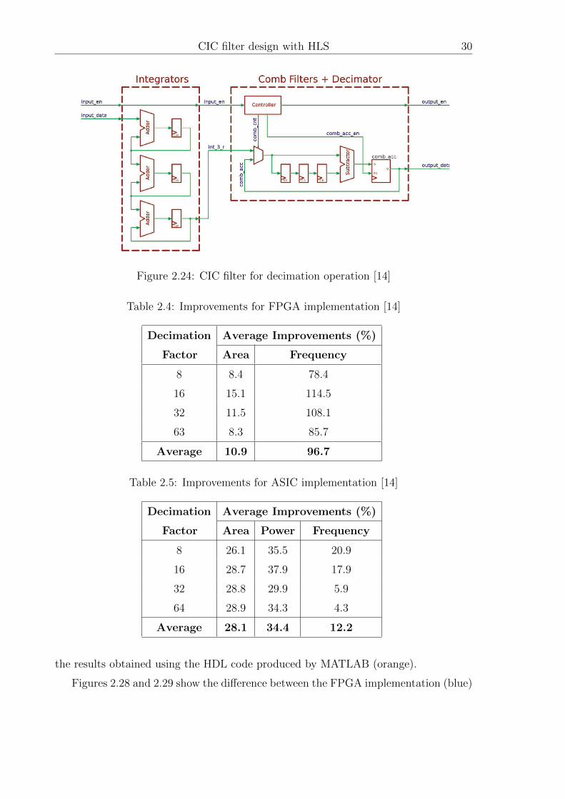
CIC filter design with HLS 30
Figure 2.24: CIC filter for decimation operation [14]
Table 2.4: Improvements for FPGA implementation [14]
Decimation
Factor
Average Improvements (%)
Area Frequency
8 8.4 78.4
16 15.1 114.5
32 11.5 108.1
63 8.3 85.7
Average 10.9 96.7
Table 2.5: Improvements for ASIC implementation [14]
Decimation
Factor
Average Improvements (%)
Area Power Frequency
8 26.1 35.5 20.9
16 28.7 37.9 17.9
32 28.8 29.9 5.9
64 28.9 34.3 4.3
Average 28.1 34.4 12.2
the results obtained using the HDL code produced by MATLAB (orange).
Figures 2.28 and 2.29 show the difference between the FPGA implementation (blue)

CIC filter design with HLS 31
Figure 2.25: Comparison of area between the optimized architecture and the one pro-
duced by the MATLAB HDL code for ASIC implementation [14]
Figure 2.26: Comparison of power between the optimized architecture and the one
produced by the MATLAB HDL code for ASIC implementation [14]
Figure 2.27: Comparison of frequency between the optimized architecture and the one
produced by the MATLAB HDL code for ASIC implementation [14]

CIC filter design with HLS 32
and the results using the MATLAB function (orange).
Figure 2.28: Comparison of area between the optimized architecture and the one pro-
duced by the MATLAB HDL code for FPGA implementation [14]
Figure 2.29: Comparison of frequency between the optimized architecture and the one
produced by the MATLAB HDL code for FPGA implementation [14]

CHAPTER 3
C++ algorithm
3.1 Reference filter specification
The case study is provided by the company Silicon Mitus, and it is a CIC filter, added
in an high-performance DAC designed to process digital stereo streaming. In particular
the CIC filter in the DAC must perform the decimation of the input samples. Silicon
Mitus provided the MATLAB behavioural description, the System Verilog description
of the architecture and the System Verilog testbench of the reference filter implemented
with the classical RTL design.
The reference CIC decimation filter has the following specifications:
• fdsd (direct digital interface frequency): possible choice between 2.8224MHz -
5.768 MHz - 11.2896 MHz - 22.5792MHz
• filter order: 6;
• downsampling rate (integer chenge rate factor): 8;
• Input parallelism: 1 bit;
• Internal parallelism: 19 bits;
• output parallelism: 19 bits.
The Direct Stream Digital interface (DSD) is based on Pulse-Density Modulation
(PDM) encoding, and it aims to store/stream a delta-sigma modulated digital audio
signal, without any coding. The input data rate can be:
33

CIC filter design with HLS 34
• DSD64: 64 times CD audio sampling rate(64*44.1kHz=2.8224MHz);
• DSD128: double-rate DSD (128*44.1kHz=5.768MHz);
• DSD256 (256*44.1kHz=11.2896);
• DSD512 (512*44.1kHz=22.5792MHz).
The top level entity of the architecture is the one shown in Figure 3.1. The architecture
consists of two independent channels, so it has two inputs ports and two outputs ports
for data stream, and another port with a signal trgo (trigger out), which is asserted
when the outputs are ready.
CLK
datai_ch1
datai_ch2
rstb
ckg_en
datao_ch1
datao_ch2
trgo
1
1
1
19
19
1
Figure 3.1: Top level entity of the architecture provided by Silicon Mitus
3.2 MATLAB code and algorithm by Silicon Mitus
The MATLAB code contains the discrete model of the CIC filter and the testbench
enviroment for the bittrue verification. The algorithm is developed as depicted in
Figure 3.2:
Digital waveform generation
The first step of the MATLAB code is to create the digital input. The function
gen dig stim produces the signals that have to be processed, by specifying the fre-
quency, the amplitude and the offset and the sine waves that have be generated. The

CIC filter design with HLS 35
Digital waveformsgenerator
Pulse DensityModulation
DC input component elimination
CIC filter algorithm
Output
Output representation on
n-bit and saturation
Figure 3.2: Structure of the MATLAB code for one single channel provided by Silicon
Mitus
function performing this generation uses also the dithering, which is a sample volun-
tary added noise, in order to reduce the quantization error when samples are quantized.
Pulse Density Modulation
The subsequent step is to perform the Pulse Density Modulation (PDM) on the quan-
tized samples coming from the function described below (gen pdm). Indeed the Direct
Stream Digital Interface is based on PDM. The PDM is a modulation to represent
an analog signal in binary code. In PDM signals the amplitude is represented by the
relative density of the pulses: a high density on 1’s implies the maximum value of
the amplitude, while a high density of 0’s implies the sine curve reaches the minimum
amplitude level. An example of Pulse Density modulated signal is shown in Figure 3.3.

CIC filter design with HLS 36
Figure 3.3: Pulse density modulation example
CIC filter algorithm
The implementation of the filter function is the next step. The dws cic bittrue function
is the core of the code and describes the discrete model of the CIC filter. The function
is divided into 3 steps: the computation of the output of the integral section, the
decimation operation, and the computation of the output of the derivative section
corresponding to the final filter output. The output of each sections are represented
inside the bit dynamics and eventually wrapped around the upper or the lower value
of the binary dynamic limit. The function performing the representation of the output
values on 19 bits is dws dyn wa, which performs also a saturation of the outputs if
needed
Golden output generation
The gen cic golden function is the function encloses the described functions. Since the
entire architecture consist of 2 channels, the function performs all of the steps previously
described twice. In particular this function generates one input per channel, it performs
the Pulse Density Modulation exploiting the gen pdm function. In this way an array
containing all the inputs is created by this function. The DC component of the digital
input is eliminated using the following equation:
input AC = (input ∗ 2) − 1 (3.1)

CIC filter design with HLS 37
Finally the input array is passed to the CIC core function dws cic bittrue and the
output array is computed.
3.3 MATLAB code translated in C++
The entire code for the production of the golden output is translated is C++.
3.3.1 The testing environment in C++
The testbench environment in C++ is structured in the same way of the one described
in MATLAB. The digital input generation is the first step for the golden output cre-
ation, so for the C++ testbench environment. By using the class vector, the time
vector and the input vector are created. Both are initialized as single element vectors,
containing a 0. The following elements are inserted by using the method push.back,
which exploits the dynamically allocated space in memory. This is necessary since
the amount of input data that the filter have to process to produce the golden output
is very high (N val = 282244). For the same reason, all of the arrays are treated as
vectors.
1 vector<double> gen_dig_stim(double amp, double f, double offset, double fs,
2 float tend, int nbit){
3 //time vector declaration and initialization
4 vector<double> t (1,0);
5 //input vector declaration and initialization
6 vector<double> vi;
7 int da=0;
8 //output vector declaration and initialization
9 vector<double> vi_int;
10 //time vector creation
11 for(unsigned i=1; i<N_val; ++i){
12 t.push_back(t[i-1]+1/fs);
13 }
14 //input vector creation

CIC filter design with HLS 38
15 for(unsigned i=0; i<N_val; ++i){
16 vi.push_back(pow(10.0,amp/20)*sin(2*pi*f*t[i])+
17 pow(10.0,(offset/20)));
18 }
19 for(unsigned i=0; i<N_val; ++i){
20 vi_int.push_back(round(vi[i]*pow(2.0,(nbit-1))-1));
21 }
22 return vi_int;
23 }
The second step is to perform the PDM.
1 vector<double> gen_pdm(double amp, double f, double offset,
2 double fs, float tend, int nb, int adddith, string file_name) {
The PDM is created by computing some vectors as show is the code above.
1 //vectors computation
2 for(unsigned i=1; i<N_val; i++){
3 //x1
4 x1.push_back(b[0]*in[i]-c[0]*y[i-1]-g[0]*int2[i-1]);
5 .
6 .
7 .
8 //u
9 u.push_back(b[4]*in[i]+a[0]*int1[i]+a[1]*int2[i]+a[2]*int3[i]+a[3]*int4[i]);
10 //y
11 int z=0; //this value is 1 if u[w]>=0, 0 otherwise. It's a logic operation
12 if (u[i]>=0){
13 z=1;
14 }
15 else
16 z=0;
17 y.push_back(z*2-1);
18 for(unsigned i=0; i<N_val; i++){

CIC filter design with HLS 39
19 mod_dout.push_back((y[i]+1)/2.0);
20 }
21 return mod_dout;
The testbench environment consists also of a function representing the output results
on 19 bits.
vector<double> dws_dyn_wa(vector<double> vi, int nbit)
By calling the function dws cic bittrue, the golden output are generated. The function
parameters are initialized as follows:
1 vo_ch1_cic=dws_cic_bittrue(cic_dwsr, vi_cic_ch1, nbdi_cic, nbdo_cic,
2 cic_ord, cic_diffdel, dec_ph);
• int cic dwsr = 8;
• int sig ch2 a = -8;
• int nbdi cic = 1;
• int nbdo cic = 19;
• int cic ord = 8;
• int cic diffdel = 2;
• int dec ph = 2;
3.3.2 Filter algorithm and its implementation
The core of the MATLAB code is the dws cic bittrue function. The function described
in C++ follows the same algorithms used by Silicon Mitus in the MATLAB code.
The C++ code exploits the class std::vector which allows to create dynamic allocated
arrays.
The function declaration is shown below.
1 vector<double> dws_cic_bittrue(int dwsr, vector<double> vi, int nbdi,
2 int nbdo, int ord, int diffdel, int dec_ph)

CIC filter design with HLS 40
• int dwsr: it is an int variable which perform decimation operation;
• vector<double> vi: it is the input vector;
• int ndbi: it is the input parallelism;
• int ndbo: it is the output parallelism;
• int ord: it is the CIC filter order;
• int diffdel: it is the differential delay;
• int dec ph: it is the decimation phase;
In the following lines the C++ code implementing the computation done by the
integral section is shown. The matrix vector<vector<double> > vint has to be com-
puted.
1 vector<vector<double> > vint;
2 vector<vector<double> >::iterator i_vint;
3 //integral loop repeated according to the CIC order
4 vint.push_back(vi);
5 for(unsigned i=1; i<=6; i++){
6 vector <double> tmp;
7 tmp.push_back(vint[i-1][0]);
8 for(unsigned j=1; j<N_val; j++){
9 tmp.push_back(vint[i-1][j]+tmp[j-1]);
10 }
11 tmp=dws_dyn_wa(tmp, num_dyn_bit, 0);
12 vint.push_back(tmp);
13 }
In Figure 3.4 the graphical representation of the integral section algorithm is reported.
When the whole matrix is computed the last row is extracted and passed as input to
the following stage, which is the decimation stage.
The aim is to create the vector vdws inserting in it one element every eight elements
of the last row of the matrix vint computed by the integral section. This operation is

CIC filter design with HLS 41
……
X_IN[0] X_IN[1] X_IN[2]IN
X_1[0]=X_IN[0]
X_1[1]=X_IN[1]+X_IN[0]
X_1[2]=X_IN[2]+X_1[1]
X_IN[n]
X_1[n]
X_N[0] X_N[1] X_N[2] X_N[n]OUT
Figure 3.4: Graphical representation of the integral section computation algorithm
performed by the counter cnt which increments its value by a dwsr value (which is 8
in the case study) as reported in Figure 3.5. This means that the vector vdws contains
a number of elements decreased by a 8 factor compared to the number of elements in
vint[6].
x0 x1 x9 x17 x25… … …
cnt=1
…
cnt=9 cnt=17 cnt=25
vint[6]
Figure 3.5: Graphical representation of the decimation stage computation algorithm
1 vector<double> vdws;
2 //discard downsampling
3 unsigned cnt=1;
4 for(unsigned i=1; i<N_val; i++){
5 if(i==cnt){
6 vdws.push_back(vint[6][i]);

CIC filter design with HLS 42
7 cnt=cnt+dwsr;
8 }
9 }
Finally, the output of the filter is computed by the derivative section. The aim is
to compute the matrix vdiff as done for the integral section following the algorithm
in Figure 3.6, which reports the graphical representation of the derivative section com-
putation algorithm. The derivative section code is shown below. Notice that the 6− th
……
X_IN[0] X_IN[1] X_IN[2]IN
X_1[0]=X_IN[0]-0
X_1[1]=X_IN[1]-X_IN[0]
X_1[2]=X_IN[2]-X_IN[1]
X_IN[n]
X_1[n]
X_N[0] X_N[1] X_N[2] X_N[n]OUT
Figure 3.6: Graphical representation of the derivative section computation algorithm
row contains the final output of the filter. All the elements of the vdiff[6] are rounded
and placed in the output vector vout.
1 vector<vector<double> > vdiff;
2 vector<vector<double> >::iterator i_vdiff;
3 vector<double> vout; //output vector
4 vdiff.push_back(vdws);
5 unsigned len_vdws=vdws.size();
6 //differential loop repeated according to the CIC order
7 for(unsigned i=1; i<=6; i++){
8 vector<double> tmp1;
9 vector<double> tmp2;

CIC filter design with HLS 43
10 tmp2.push_back(0.0);
11 for(unsigned j=0; j<len_vdws-1; j++){
12 tmp2.push_back(vdiff[i-1][j]);
13 }
14 for(unsigned k=0; k<len_vdws; k++){
15 tmp1.push_back(vdiff[i-1][k]-tmp2[k]);
16 }
17 tmp1=dws_dyn_wa(tmp1, num_dyn_bit, 0);
18 vdiff.push_back(tmp1);
19 }
20 for(unsigned i=0; i<len_vdws; i++){
21 vout.push_back(floor(vdiff[6][i]*pow(2,(nbdo-num_dyn_bit))+0.5));
22 }
23 return vout;
24 }
3.4 C++ code to synthesize the CIC filter
Once the whole MATLAB code is translated in C++, the idea is to isolate the core
function and to pass it in Catapult so that it can be synthesized and the RTL descrip-
tion of the architecture can produced.
The CIC function implemented as described is the previous section, produces the out-
put with an algorithm which takes into account the number of samples at the input.
In order to allow Catapult to work, the described function has to get rid of the depen-
dence from the input.
The first step is to re-think about the algorithm.
Integrative section algorithm
In Figure 3.7 the basic principle of the new integrative section algorithm is reported.
In this case only two arrays are used: outsum and integ. The number of elements in
the array integ is 6, as the filter order value is, while the elements in the array outsum
is 7, so the value of the CIC filter order plus one element which is the incoming input.

CIC filter design with HLS 44
Figure 3.7: The basic principle of the integrative algorithm
Every time an input occurs the function is called and the outsum array computed
in the previews function call is copied in the array integ. Then the array outsum
is computed by using the array integ, where the values of outsum computed in the
previous function call are stored.
Derivative section algorithm
For the derivative section the new algorithm is similar to the one of the integrative
section, as reported in Figure 3.8. Also in this case the number of elements in the
outdiff array is order + 1, so 7, while the elements in the diff array is ord, so 6.
That’s because the last elements of the array coming from the decimation stage is
stored is the array outdiff .
The derivative section provides the final output of the filter, which is the last element
of the array outdiff .

CIC filter design with HLS 45
outdiff[5]
outdiff[4]
outdiff[3]
outdiff[2]
outdiff[1]
outdiff[0]
outdiff[6]
diff[5]
diff[4]
diff[3]
diff[2]
diff[1]
diff[0] -
-
-
-
-
-
=
=
=
=
=
=
outdiff[7]diff[6]
Figure 3.8: The basic principle of the derivative section algorithm
The synthesizable code
In the following lines the implementation of a CIC filter is shown.
1 double dws_cic_bittrue(double vi, int ord){
2 static double integ[ord];
3 static double outsum[ord+1];
4 static unsigned in_cnt = 0;
5
6 static double diff[ord];
7 static double outdiff[ord+1];
8
9 INTEGRAL_COPY_LOOP: for( int i=0; i<ord; i++){
10 integ[i]=outsum[i+1];

CIC filter design with HLS 46
11 }
12 outsum[0] = vi;
13 INTEGRAL_LOOP: for (int i=0; i<ord; i++){
14 outsum[i+1]=dws_dyn_wa(outsum[i]+integ[i], 19, 0);
15 }
16 if(in_cnt==1 || (in_cnt-1)%8==0){
17 DERIVATIVE_COPY_LOOP: for(int i=ord-1; i>=0; i--){
18 diff[i] = outdiff[i];
19 }
20 outdiff[0] = outsum[ord];
21 DERIVATIVE_LOOP: for (int i=0; i<ord; i++){
22 outdiff[i+1]=dws_dyn_wa(outdiff[i]-diff[i], 19, 0);
23 }
24 }
25 in_cnt++;
26 return outdiff[ord];
27 }
The code shown above implements one filter’s channel. For sake of simplicity the
part of the code implementing the second channel in missing, because it is exactly
identical to the one of the first channel. The entire code is shown in appendix A.1.
The elements of the arrays outsum, outdiff , integ, diff are declared as ’double’,
as done in the previous C++ code in order to compare the output results with the
golden output produced by the MATLAB code or by the C++ code. The arrays are
also declared as ’static’, because the data computed after each function call can be
reused when a new input has to be processed. This is useful for the arrays integ and
diff , because their previous content is directly involved in the sum and the subtraction
operations in integrative and derivative sections. The arrays outsum and outdiff are
also ’static’ because in each function call their content from the previous computation
is copied in integ and diff arrays.
For this code production, the parallelism of the input, intermediate and output data
is not used to define the variables, so, in order to compare the results of this code with
the once of the previous code it is necessary to use the function to represent the output

CIC filter design with HLS 47
values into the binary dynamic (dws dyn wa).
The code structure is composed by four for statements. Each section is described
using two independent loops: the first one is dedicated to the Copy ; the second one
is referred to the operation that has to be performed. In the Copy Loops the storing
in the arrays integ and in diff of all the elements of the arrays outsum and outdiff
is performed. The Integral Loop or the Derivative Loop allow the operations (sum for
integration and subtraction for derivation).
A counter (in cnt) is also instantiated as ’unsigned’. It has the function to discard
samples processed by the integral section in order to send the only the useful samples
to the derivative section. In particular it is necessary to send to the derivative section
the second integrated sample and one integrated sample every eight computed by the
integrative section. This discard operation is implemented using the if statement.
When the condition is verified, the derivative section is enabled, so it can work, too.
Optimized synthesizable code
Since Catapult is able to use variables with data types that take into account the
parallelism of the data, it is useful to use this declaration of variables exploiting the
arbitrary-length bit-accurate integer and fixed-point datatypes. The ac int represen-
tation was used, and in particular the following data types are exploited all around the
design:
• IN TY PE(ac int < 1, false >): the input of the CIC filter are 1-bit unsigned
data;
• CNT TY PE(ac int < 3, false >): the counter performing decimation is a mod-
ulo 8 counter, so it is a 3bit unsigned number;
• AC TY PE s(ac int < 2, true >): the filter requires to work with samples with-
out the DC component. To perform this operation, the input datum equal to 0
has to be represent as -1, while the input datum equal to 1 remains 1. In order
to represent correctly this values, a 2bit signed representation is required;
• OUT TY PE(ac int < 19, false >): all the value processed by every stage of
the integrative and derivative sections and given as output are represent as 19bit
unsigned numbers.

CIC filter design with HLS 48
1 void dws_cic_bittrue(IN_TYPE vi_ch1, IN_TYPE vi_ch2,
2 OUT_TYPE &out_cic_ch1, OUT_TYPE &out_cic_ch2){
3
4 static OUT_TYPE integ_ch1[ord];
5 static OUT_TYPE outsum_ch1[ord+1];
6 static CNT_TYPE in_cnt_ch1 = 7;
7 static OUT_TYPE diff_ch1[ord];
8 static OUT_TYPE outdiff_ch1[ord+1];
9
10 AC_TYPE_s vi_ac_ch1;
11 vi_ac_ch1 = AC_TYPE_s(vi_ch1)*2 - 1;
12
13 INTEGRAL_COPY_LOOP1: for( int i=0; i<ord; i++){
14 integ_ch1[i]=outsum_ch1[i+1];
15 }
16 outsum_ch1[0] = OUT_TYPE(vi_ac_ch1);
17 INTEGRAL_LOOP1: for (int i=0; i<ord; i++){
18 outsum_ch1[i+1]=outsum_ch1[i]+integ_ch1[i];
19 }
20 if(in_cnt_ch1==0){
21 DIFFERENTIAL_COPY_LOOP1: for(int i=ord-1; i>=0; i--){
22 diff_ch1[i] = outdiff_ch1[i];
23 }
24 outdiff_ch1[0] = outsum_ch1[ord];
25 DIFFERENTIAL_LOOP1: for (int i=0; i<ord; i++){
26 outdiff_ch1[i+1]=outdiff_ch1[i]-diff_ch1[i];
27 }
28 }
29 in_cnt_ch1++;
30 out_cic_ch1 = outdiff_ch1[ord];
31 }
Notice the counter (in cnt ch1) instantiated used to do the decimation operation as

CIC filter design with HLS 49
described previously. In this case the initialization of the counter is at the value 7.
The code written in this way allows Catapult to synthesize the architecture, because
the C++ description algorithm is totally independent from the input.

CHAPTER 4
CIC filter development with Catapult
In this chapter, the design of the CIC filter using Catapult is described. From the C++
algorithm description, the RTL code is produced by Catapult and the results obtained
using Catapult during the pre-synthesis phase, and the ones produced by Synopsys
during the post-synthesis phase are described and compared. In particular the results
in terms of area and power consumption are shown and the differences between the
explored solutions are reported. The aim of the work is to demonstrate that by using
HLS it is possible to obtain high quality implementations. This aim is obtained by
comparing the architecture synthesized by using the HLS tool Catapult, with the one
produced by Silicon Mitus which is implemented with the classical hand-written RTL
design. Figure 4.1 reports a section of the simulation of the reference architecture, with
both the channels. The output sample rate of the architecture is fs out = 1/R ∗ fs in,
-5 -259 1...
0 0 ...0 ...0
-5 -259 1...
0 ...0 ...0 ...0
0 ps 10000 ps
/tb_cic_top/clk_2p8m
/tb_cic_top/data_ch1
/tb_cic_top/ckg_en
/tb_cic_top/cic_trgo
...c_top/cic_datao_ch1_reg -5 -259 1...
/tb_cic_top/cic_datao_ch1 0 0 ...0 ...0
/tb_cic_top/data_ch2
...c_top/cic_datao_ch2_reg -5 -259 1...
/tb_cic_top/cic_datao_ch2 0 ...0 ...0 ...0
8 clock cycles
-5
Figure 4.1: ModelSim simulation of the reference architecture by Silicon Mitus
50

CIC filter design with HLS 51
where R is the decimation factor, which is 8 in this case, and fs in is the input sample
rate equal to 2.8224MHz. It means that the output is updated every 8 clock cycles as
it is reported in Figure 4.1.
4.1 Correctness verification of the synthesized ar-
chitecture
The first step is to evaluate if the architecture generated by Catapult provides the
corrected output. In order to do this SCV erify is enabled. In order to perform
this step a testbench in C++ is written. SCV erify uses ModelSim to simulate the
architecture and to check that no output errors occur. The synthesis in this step is
done by Catapult, without using any specific setting. Once Catapult terminates the
synthesis and produces the RLT description of the architecture, SCV erify creates a
SystemC wrapper, which tests the architecture, and compare the results with the ones
produced by the C++ testbench, as described in Chapter1. In the following lines the
testbench written in C++ is reported. The input are taken from a .txt file. For sake
of simplicity only the management of the file containing the input of the first channel
is shown, while the entire code is shown in Appendix A.2.
1 CCS_MAIN(int argc, char **argv) // required for sc verify flow in
2 // Catapult
3 {
4 ifstream in_ch1 ("cic_in_ch1.txt", ios::in);
5 vector<IN_TYPE> vi_cic_ch1;
6 int in1; //in1=[0 o 1], in1_bin=[-1 o 1]
7 OUT_TYPE in1_bin;
8 OUT_TYPE vout_cic_ch1;
9 vector<OUT_TYPE> cic_output_ch1;
10 while(!in_ch1.eof()){
11 in_ch1>>in1;
12 vi_cic_ch1.push_back(IN_TYPE(in1));
13 }

CIC filter design with HLS 52
14 in_ch1.close();
15
16 //the same is done for channel 2//
17
18 for (unsigned i=0; i<vi_cic_ch1.size(); i++){
19 CCS_DESIGN(dws_cic_bittrue)(vi_cic_ch1[i], vi_cic_ch2[i],
20 vout_cic_ch1, vout_cic_ch2);
21 }
22 CCS_RETURN(0);
23 }
The input are stored in a vector containing elements, whose data type is IN TY PE,
so 1bit unsigned elements. Every time an input occurs the function is called. The
produced output are stored in the vector of OUT TY PE elements (19 bits signed).
As shown in the ModelSim message below, there are no errors, so no mismatches
between the output produced by the architecture, and the one produced by the C++
testbench.
# Info: Execution of user -supplied C++ testbench 'main()' has
completed with exit code = 0
#
# Info: Collecting data completed
# captured 284 values of vi_ch1
# captured 284 values of vi_ch2
# captured 284 values of out_cic_ch1
# captured 284 values of out_cic_ch2
# Info: scverify_top/user_tb: Simulation completed
#
# Checking results
# 'out_cic_ch1 '
# capture count = 284
# comparison count = 284
# ignore count = 0
# error count = 0
# stuck in dut fifo = 0
# stuck in golden fifo = 0
# 'out_cic_ch2 '

CIC filter design with HLS 53
# capture count = 284
# comparison count = 284
# ignore count = 0
# error count = 0
# stuck in dut fifo = 0
# stuck in golden fifo = 0
#
# Info: scverify_top/user_tb: Simulation PASSED 1083657975 ps
The Figure 4.2 shows the ModelSim simulation done using SCV erify. The signals
out cic ch1−ERR# and out cic ch2−ERR# counts the output errors, which are 0 in
this case, remarking the correct behavior of the architecture. The data out cic ch1 −GOLDEN and out cic ch2 − GOLDEN are the output data produced by the C++
testbench in appendix A.2, while the data out cic ch1−DUT and out cic ch2−DUT
are produced by the SystemC wrapper testbench produced by SCV erify.
... -19’d5 -19’d259 19’d1524 19’d4226 19’d6459 19’d... 19’d... 19’d... 19’d... ...
... -19’d5 -19’d259 19’d1524 19’d4226 19’d6459 19’d... 19’d... 19’d... 19’d... ...
32’h0
... -19’d5 -19’d259 19’d1046 19’d1120 19’d2021 19’d4799 19’d8430 19’d7656 19’d... ...
... -19’d5 -19’d259 19’d1046 19’d1120 19’d2021 19’d4799 19’d8430 19’d7656 19’d... ...
32’h0
0 ps+10 200000000 ps 400000000 ps
out_cic_ch1-GOLDEN ... -19’d5 -19’d259 19’d1524 19’d4226 19’d6459 19’d... 19’d... 19’d... 19’d... ...
out_cic_ch1-DUT ... -19’d5 -19’d259 19’d1524 19’d4226 19’d6459 19’d... 19’d... 19’d... 19’d... ...
out_cic_ch1-ERR# 32’h0
out_cic_ch2-GOLDEN ... -19’d5 -19’d259 19’d1046 19’d1120 19’d2021 19’d4799 19’d8430 19’d7656 19’d... ...
out_cic_ch2-DUT ... -19’d5 -19’d259 19’d1046 19’d1120 19’d2021 19’d4799 19’d8430 19’d7656 19’d... ...
out_cic_ch2-ERR# 32’h0
Figure 4.2: ModelSim simulation shows the correct behaviour of the architecture pro-
duced by Catapult
4.2 Different architectures of the CIC filter and
Catapult results
Once the correctness of the architecture is verified, it is possible to proceed to explore
different architectural solutions to evaluate what is the best in terms of area power
and timing. This process is done by exploiting the Catapult synthesis first, and then

CIC filter design with HLS 54
generating the gate-level code with Synopsys Design Compiler, starting from the
Verilog RTL code produced by Catapult.
Starting from the code described in appendix A.1, the Catapult synthesis is performed
by using as clock frequency 2.8224MHz and 45nm target technology.
The Table 4.1 shows the timing results from Catapult synthesis. Note that the different
simulations are produced without changing the C++ code, but by simply changing the
simulation parameters described in Chapter1. The code is synthesized to create folded
architecture (F), first. Then different unfolding grade (U) and initiation intervals (P)
are applied.
Catapult results
Architecture solutions Latency cycles Throughput cycles Slack(ns)
F 40 41 352.3
P=1 F 36 36 353.28
P=1 U=2 18 18 352.74
P=1 U=3 12 12 352.09
P=1 U=4 16 16 351.56
P=1 U=5 16 16 350.8
P=1 U=6 1 1 337.42
Table 4.1: Catapult results in terms of latency an throughput cycles and slack time
The architecture full-unrolled (U=6) and with an initiation interval 1 (P=1) is the
one more interesting because it reflects the timing behavior of the reference architecture.
The Figure 4.3 explain the reason why Catapult evaluation of the throughput is 1.
Every output is written of the bus 8 times. The signal out cic ch1 − TRANS# and
out cic ch2 − TRANS# counts the number of transition on the output buses, so the
number of transactions on the bus is 8, per every output. This means that this behavior
is similar to the one of the reference architecture provided by Silicon Mitus, shown in
Figure 4.1.
The Table 4.2 shows what are the allocated resources in the different architectural
solution. Notice that folded architecture has the highest area. That’s because the op-
eration of the INTEGRAL COPY LOOP and the DERIVATIVE COPY LOOP are implemented

CIC filter design with HLS 55
19’d0 -19’d5 -19’d259 19’d1524
19’d0 -19’d5 -19’d259 19’d1046
32’h0 3... 3... 3... 3... 3... 3... 3... 3... 3... 3... 3... 3... 3... 3... 3... 3... 3... 3... ...
32’h0
32’h0 3... 3... 3... 3... 3... 3... 3... 3... 3... 3... 3... 3... 3... 3... 3... 3... 3... 3... ...
32’h0
clk
vi_ch1_rsc_dat
vi_ch2_rsc_dat
out_cic_ch1_rsc_dat 19’d0 -19’d5 -19’d259 19’d1524
out_cic_ch2_rsc_dat 19’d0 -19’d5 -19’d259 19’d1046
out_cic_ch1-TRANS# 32’h0 3... 3... 3... 3... 3... 3... 3... 3... 3... 3... 3... 3... 3... 3... 3... 3... 3... 3... ...
out_cic_ch1-ERR# 32’h0
out_cic_ch2-TRANS# 32’h0 3... 3... 3... 3... 3... 3... 3... 3... 3... 3... 3... 3... 3... 3... 3... 3... 3... 3... ...
out_cic_ch2-ERR# 32’h0
8 output transitions
Figure 4.3: Simulation by SCV erify
with 102 multiplexers with 19 bits of input parallelism, which impact the total area
of the folded structure dramatically. The use of a very large number of multiplexers
require a large amount of instantiated registers.
The Figure 4.4 reports how much multiplexers, registers, functional units and logic
affect the area of the different architectural solutions. Notice the absence of multiplex-
ers and a few number of registers instantiated in the full-unrolled architecture. This
architecture allows resource sharing and so its total area is the lowest possible.
As expected the solutions with higher unfolding grade have larger area, except for
the full-unfolding architecture, for the reason discussed before.
The Table 4.3 reports the results obtained using Synopsys Design Compiler. Note
that also with the synthesis done by the actual logic synthesizer, the full-unrolling
architecture keeps the primacy in terms of area, and it is also the solution with the
lowest power consumption. For this reason, the full-unrolled architecture is developed
with the aim of obtaining an architecture whose performance are as close as possible
to the reference one designed by Silicon Mitus
4.3 Final architecture and optimizations
In order to better understand if an architecture designed using HLS can have perfor-
mance which are comparable with the ones obtained using the classical RTL design,
it is necessary to design an architecture which could replace the reference one, which
means to use for the synthesized architecture to use the same interface signals of the

CIC filter design with HLS 56
Allocated resources Total area µm2
Adders Multiplexers RegistersArchitectural solutions Number Parallelism Number Parallelism Number Parallelism
F 1 4bit 3 3bit 11 3bit 21946.45
4 3bit 102 19bit 121 19bit1 19bit
P=1 F 2 4bit 12 19bit 12 3bit 8594.17
14 3bit 6 1bit 1 2bit4 19bit 10 3bit 40 19bit
11 1bit
P=1 U=2 2 3bit 10 2bit 4 3bit 8570.85
8 2bit 18 19bit 9 2bit8 19bit 6 1bit 40 19bit
11 1bit
P=1 U=3 16 3bit 22 19bit 4 3bit 9603.20
6 2bit 16 1bit 1 2bit12 19bit 4 3bit 40 19bit
23 1bit
P=1 U=4 2 3bit 14 19bit 4 3bit 10386.4
16 19bit 10 1bit 1 2bit52 19bit19 1bit
P=1 U=5 2 4bit 18 19bit 4 3bit 11884.62
8 3bit 19 1bit 1 2bit2 2bit 52 19bit20 19bit 27 1bit
P=1 U=6 2 3bit 0 - 2 3bit 5163.6
24 19bit 0 - 24 19bit2 19bit3 1bit
Table 4.2: The table shows the resources allocated by Catapult for the different archi-
tectural solutions
reference ones. The architecture produced by Silicon Mitus is the one reported in
Figure 4.5.
The interface signals are:
• rstb: it is the asynchronous reset of the architecture, which creates the internal
synchronous reset;

CIC filter design with HLS 57
0
5000
10000
15000
20000
25000
F P=1 F P=1 U=2 P=1 U=3 P=1 U=4 P=1 U=5 P=1 U=6
REG 16834,7 5929,9 5913,9 5857,9 7477,9 7606,2 3201,4
LOGIC 379,2 257,8 342,8 288,1 311,6 356,5 103,3
FUNCT 154,2 773,4 1114,2 1728,6 2077,2 2614,6 1807,3
MUX 4510,3 1632,9 1285,62 1632,5 519,3 1188,4 0
Area(µm^2)
Architectural solutions
MUX FUNCT LOGIC REG
Figure 4.4: How multiplexers, registers, functional units and logic affect the area of
the different architectures
Unfolding grade Area(µm2) Power(µW ) Dynamic / Leakage Time(ns) Slack / Arrival time
F 17007.50 47.88 / 388.51 351.05 / 3.13
P=1 F 6563.81 16.20 / 136.85 351.58 / 2.60
P=1 U=2 6517.26 16.15 / 142.46 351.47 / 2.71
P=1 U=3 6738.31 16.27 / 145.34 351.35 / 2.83
P=1 U=4 8154.22 20.24 / 174.02 351.6 / 2.58
P=1 U=5 8843.96 20.64 / 186.78 351.26 / 2.92
P=1 U=6 5163.59 12.52 / 94.77 350.21 / 3.97
Table 4.3: Synopsys results
• data ch1 and data ch2: they are the 1bit input data of the two filters;
• ckg en: it is the clock enable to perform the clock gating;

CIC filter design with HLS 58
rstb
clk
ckg_en
data_ch1
data_ch2
cic_datao_ch1
cic_datao_ch2
cic_trgo
1
1
1
1
1
19
19
Figure 4.5: Silicon Mitus architecture (top view)
• clk: it is the clock. Its frequency is 2.8224MHz;
• cic datao ch1 and cic datao ch1: are the 19bit filters output data;
• trgo: it is the signal indicating when the output is ready.
In this case the architecture design with HLS has to include a clock enable and an
asynchronous reset. Moreover, the reference architecture, by Silicon Mitus, produces
internally a synchronous reset starting from the asynchronous reset (rstb) and the clock
enable (ckg en). The synchronous reset has the aim to reset all the internal registers
of both the filters. For the architecture produced with the HLS methodology, enable,
clock and reset signals can be added to the architecture without changing the code.
The clock, enable and reset signals are set as follows:
• clk: the clock frequency is 2.8224MHz and the data sampling is performed on its
rising edge;
• rst: the synchronous reset is high-active;
• arst n: the asynchronous reset is low-active;
• en: the clock enable is high-active.
The full-unrolled architecture is developed and the Catapult results are:

CIC filter design with HLS 59
CIC1
CIC2
LOGIC
rstb
ckg_ensync_rst
data_ch1
data_ch2
cic_datao_ch1
cic_datao_ch2
clk
trgo
cic_en
Figure 4.6: Internal structure of the reference architecture bt Silicon Mitus
Figure 4.7: Clock setting
• Slack cycle: 1;
• Throughput cycle: 1;
• Area: 6204.05 µm2;
• Slack time: 337.39 ns.

CIC filter design with HLS 60
Figure 4.8: Signal setting
Catapult uses triosy lz signals for each C++ variable to indicate the I/O completion
of the associated signals. In order to avoid these signals at the architecture interface
it is possible to use the interface using ac channel interface. This latter solves the
problem to build a streaming interface to guarantee that the data communication is
correct, so that data are read and written in the same order they are processed. So,
the ac channel interface constructs a FIFO discipline to ensure the correctness of the
communication between different blocks.
The C++ code is slightly modified to allow the synthesis using acchannel interface.
1 #include <ac_fixed>
2 #include <ac_channel>
3 const unsigned ord = 6;
4 typedef ac_int<1,false> IN_TYPE;
5 typedef ac_int<2,true> AC_TYPE_s;
6 typedef ac_int<19, true> OUT_TYPE;
7 typedef ac_int<1, false> BIT_TYPE;
8
9 void dws_cic_bittrue(ac_channel<IN_TYPE> &, ac_channel<IN_TYPE> &,
10 ac_channel<IN_TYPE> &, ac_channel<OUT_TYPE> &, ac_channel<OUT_TYPE> &,
11 BIT_TYPE &ready_out);
Once the directive to synthesize a full-unrolled architecture are set, the Catapult results
are:

CIC filter design with HLS 61
• Slack cycle: 1;
• Throughput cycle: 1;
• Area: 6767.38 µm2;
• Slack time: 337.25 ns.
This architecture is larger than the one implemented without acchannel interface. For
this reason the solution without ac channel interface is preferred.
4.3.1 Architecture functioning
The top view of this architecture synthesized by Catapult is the one represented in
Figure 4.9.
arst_n
clk
en
vi_ch1_rsc_dat out_cic_ch1_rsc_dat
ready_out_rsc_dat
1
1
1
1
1
19
19
out_cic_ch2_rsc_datvi_ch2_rsc_dat
out_cic_ch1_rsc_triosy_lz
out_cic_ch2_rsc_triosy_lz
vi_ch2_rsc_triosy_lz
vi_ch1_rsc_triosy_lz
ready_out_rsc_triosy_lz
1
1
1
1
1
rst
Figure 4.9: Top view designed by Catapult
The triosy lz signals enlarge the total area and make the architecture interface
(Figure 4.9) different from the one of the reference architecture (Figure 4.5). So the
solution is to eliminate them by hand in the Verilog code produced by Catapult, with
a very small effort. The resulting architecture is the one reported in Figure 4.10.
Table 4.4 reports that the results evaluated with Catapult and Synopsys are slightly
different but with the same behaviour, as shown in Figure 4.11.

CIC filter design with HLS 62
arst_n
clk
en
vi_ch1_rsc_dat out_cic_ch1_rsc_dat
ready_out_rsc_dat
1
1
1
1
1
19
19
out_cic_ch2_rsc_datvi_ch2_rsc_dat
rst
Figure 4.10: Top view of the optimized architecture
19191,9
70806841,8 7098,5
8749,8 9165
5025,3
24229,05
9425,25 9379,13 10386,3511328,44
12831,87
6070,72
0
5000
10000
15000
20000
25000
30000
F P=2 F P=2 U=2 P=2 U=3 P=2 U=4 P=2 U=5 P=2 U=6
AR
EA
ARCHITECTURAL SOLUTIONS
CATAPULT VS SYNOPSYS-AREA EVALUATION
Synopsys Catapult
(µ𝑚
2)
Figure 4.11: Area estimation: Catapult vs Synopsys
Notice that the Table 4.4 reports two full-unrolling solutions. By using the architec-
ture full-unrolled and with an initiation interval equal to 2 the area is lower compared
to the full-unrolled architecture with initiation interval 1.
The solution with P=2 can take as input the signals with a sample rate 2.8224MHz,

CIC filter design with HLS 63
but it has to use as internal frequency for the processing task 5.768MHz. In the DAC
design by Silicon Mitus, it is not possible to use two clock regimes, so this solution is
not further developed.
Tables 4.5 and 4.6 shows the difference in percentage between the Catapult architec-
ture and the reference architecture by Silicon Mitus. The architecture selected for the
Unfolding gradeArea by
Synopsys(µm2)
Area by
Catapult(µm2)
Power
Dynamic/
Leakage (µW )
Time Slack/
Arrival time
by Synopsys
(ns)
Time Slack/
Arrival time
by Catapult
(ns)
F 19191,9 24229,05 50,17/349,45 351,05/3,13 352,29
P=2 F 7080,0 9425,25 17,28/144,96 351,58/2,60 353,26
P=2 U=2 6841,8 9379,13 17,28/140,91 351,47/2,71 352,72
P=2 U=3 7098,5 10386,35 17,25/143,77 351,35/2,83 352,08
P=2 U=4 8749,8 11328,44 21,72/166,61 351,6/2,58 351,54
P=2 U=5 9165,0 12831,87 21,97/154,95 351,26/2,92 350,78
P=2 U=6 5025,3 6070,72 13,64/93,32 350,21/3,97 337,25
P=1 U=6 5402,9 6204,05 12,96/88,53 350,34/3,85 337,39
Table 4.4: Catapult and Synopsys results of the final architecture
comparison with the reference architecture provided by Silicon Mitus, is the full un-
rolled one, with initiation interval 1 (P=1 U=6). By using Synopsys Design Compiler
the logic synthesis is performed. The synthesis results differences between the Silicon
Mitus architecture and the Catapult architecture are performed by using the Compile
and the Compile ultra directives, and are reported in Table 4.5.
Notice that the with the architecture synthesized with the Compile ultra directive the
area and the power consumption of the architecture implemented with Catapult are
lower that the one of the architecture implemented by using the classical RTL design
methodology. In Table 4.6 the difference of the results of the logic synthesis between
the two architecture are highlighted.
In this way the aim to demonstrate the good quality production of a HLS synthesis
is achieved.

CIC filter design with HLS 64
Catapult Silicon Mitus
Compile Compile Ultra Compile Compile Ultra
Area (µm2) 6002.02 5402.99 5993.78 5564.64
Power Dyn/Stat (µW ) 14.07 / 101.93 12.96 / 88.53 12.14 / 102.85 12.04 / 94.1
Time Slack/Arrival (ns) 350.20 / 3.99 350.34 / 3.85 351.11 / 2.62 351.21 / 2.61
Table 4.5: Catapult final architecture evaluated with Synopys
Catapult
Compile Compile Ultra
Area +0.14% -2.9%
Power Dyn/Stat +0.88% -4.38%
Time Slack/Arrival (ns) +1.37 +1.24
Table 4.6: Catapult final architecture comparisons with Silicon Mitus architecture

CHAPTER 5
Conclusion
The thesis work aims to evaluate the quality of the architecture implemented by us-
ing the HLS design methodology. The area, timing and power estimation difference
between the hand-written RTL reference design and the one developed with HLS is
summarized below.
Catapult
Area -2.9%
Power Dyn/Stat -4.38%
Time Slack/Arrival (ns) +1.24
The performance results in this case study are even better than the one obtained with
the hand-written RTL design. This means that from the current generation of HLS, it
is possible to consider it as a valid design methodology, with results very close to the
ones of the well-optimized classical RTL design.
The great advantage of design implemented with HLS is the very low time consuming
to implement different architectural solutions, since it is simply necessary to properly
set the constraints in the HLS tool, without changing the HLL description algorithm.
In this way, a very high effort can be dedicated to the algorithm optimization, instead
of writing HDL code.
Another important aspect of HLS is the highly reduced effort for verification flow. The
fast development of the test is another way to improve productivity.
In conclusion, the HLS can represent a very efficient mean for digital architectures
65

CIC filter design with HLS 66
design, which can lead to high quality results, with a small effort from the designer,
who can avoid the redundant work of writing HDL code by hand.

APPENDIX A
Code
A.1 Synthesizable code
1 void dws_cic_bittrue(IN_TYPE vi_ch1, IN_TYPE vi_ch2,
2 OUT_TYPE &out_cic_ch1, OUT_TYPE &out_cic_ch2){
3
4 static OUT_TYPE integ_ch1[ord];
5 static OUT_TYPE outsum_ch1[ord+1];
6 static CNT_TYPE in_cnt_ch1 = 7;
7 static OUT_TYPE diff_ch1[ord];
8 static OUT_TYPE outdiff_ch1[ord+1];
9 AC_TYPE_s vi_ac_ch1;
10 vi_ac_ch1 = AC_TYPE_s(vi_ch1)*2 - 1;
11
12 static OUT_TYPE integ_ch2[ord];
13 static OUT_TYPE outsum_ch2[ord+1];
14 static CNT_TYPE in_cnt_ch2 = 7;
15 static OUT_TYPE diff_ch2[ord];
16 static OUT_TYPE outdiff_ch2[ord+1];
17 AC_TYPE_s vi_ac_ch2;
18 vi_ac_ch2 = AC_TYPE_s(vi_ch2)*2 - 1;
19
20 INTEGRAL_COPY_LOOP1: for( int i=0; i<ord; i++){
21 integ_ch1[i]=outsum_ch1[i+1];
67

CIC filter design with HLS 68
22 }
23 outsum_ch1[0] = OUT_TYPE(vi_ac_ch1);
24 INTEGRAL_LOOP1: for (int i=0; i<ord; i++){
25 outsum_ch1[i+1]=outsum_ch1[i]+integ_ch1[i];
26 }
27 if(in_cnt_ch1==0){
28 DIFFERENTIAL_COPY_LOOP1: for(int i=ord-1; i>=0; i--){
29 diff_ch1[i] = outdiff_ch1[i];
30 }
31 outdiff_ch1[0] = outsum_ch1[ord];
32 DIFFERENTIAL_LOOP1: for (int i=0; i<ord; i++){
33 outdiff_ch1[i+1]=outdiff_ch1[i]-diff_ch1[i];
34 }
35 }
36 in_cnt_ch1++;
37 out_cic_ch1 = outdiff_ch1[ord];
38
39 INTEGRAL_COPY_LOOP1: for( int i=0; i<ord; i++){
40 integ_ch2[i]=outsum_ch2[i+1];
41 }
42 outsum_ch2[0] = OUT_TYPE(vi_ac_ch2);
43 INTEGRAL_LOOP2: for (int i=0; i<ord; i++){
44 outsum_ch2[i+1]=outsum_ch2[i]+integ_ch2[i];
45 }
46 if(in_cnt_ch2==0){
47 DIFFERENTIAL_COPY_LOOP2: for(int i=ord-1; i>=0; i--){
48 diff_ch2[i] = outdiff_ch2[i];
49 }
50 outdiff_ch2[0] = outsum_ch2[ord];
51 DIFFERENTIAL_LOOP2: for (int i=0; i<ord; i++){
52 outdiff_ch2[i+1]=outdiff_ch2[i]-diff_ch2[i];
53 }
54 }
55 in_cnt_ch2++;

CIC filter design with HLS 69
56 out_cic_ch2 = outdiff_ch2[ord];
57
58 }
A.2 C++ Testbench
1 #include "cic_synt.h"
2 #include <mc_scverify.h>
3 using namespace std;
4
5 CCS_MAIN(int argc, char **argv) // required for sc verify flow in Catapult
6 {
7 ifstream in_ch1 ("cic_in_ch1.txt", ios::in);
8 if(!in_ch1.is_open()){
9 cout<<"Opening error of the input file on the channel1"<<endl;
10 return -1;
11 }
12 vector<IN_TYPE> vi_cic_ch1;
13 int in1; //in1=[0 o 1], in1_bin=[-1 o 1]
14 OUT_TYPE in1_bin;
15 OUT_TYPE vout_cic_ch1;
16 vector<OUT_TYPE> cic_output_ch1;
17 while(!in_ch1.eof()){
18 in_ch1>>in1;
19 vi_cic_ch1.push_back(IN_TYPE(in1));
20 }
21 in_ch1.close();
22
23 ifstream in_ch2 ("cic_in_ch2.txt", ios::in);
24 if(!in_ch2.is_open()){
25 cout<<"Opening error of the input file of the channel2"<<endl;
26 return -1;
27 }
28 vector<IN_TYPE> vi_cic_ch2;

CIC filter design with HLS 70
29 int in2; //in1=[0 o 1], in1_bin=[-1 o 1]
30 OUT_TYPE in2_bin;
31 OUT_TYPE vout_cic_ch2;
32 vector<OUT_TYPE> cic_output_ch2;
33 while(!in_ch2.eof()){
34 in_ch2>>in2;
35 vi_cic_ch2.push_back(IN_TYPE(in2));
36 }
37 in_ch2.close();
38
39 ofstream out_ch1 ("cic_filter_out_ch1.txt");
40 ofstream out_ch2 ("cic_filter_out_ch2.txt");
41 for (unsigned i=0; i<vi_cic_ch1.size(); i++){
42 CCS_DESIGN(dws_cic_bittrue)(vi_cic_ch1[i], vi_cic_ch2[i],
43 vout_cic_ch1, vout_cic_ch2);
44 if (i==1 || (i-1)%8==0){
45 out_ch1<<vout_cic_ch1<<endl;
46 out_ch2<<vout_cic_ch2<<endl;
47 }
48 }
49 out_ch1.close();
50 out_ch2.close();
51 CCS_RETURN(0);
52 }

Bibliography
[1] P. Coussy, D. D. Gajski, M. Meredith, and A. Takach, ”An Introduction to High-
Level Synthesis”, IEEE Design & Test of Computers, vol. 26, no. 4, 2009 iii,
3
[2] Grant Martin, Gary Smith, ”High-Level Synthesis: Past, Present, and Future”,
IEEE Design & Test of Computers, July/August 2009 4, 5
[3] Mojtaba Mahdavi, ”High Level Synthesis with Catapult”, DSP Design Course,
EIT Department, Lund University, Sweden
[4] Catapult Documentation viewer, Mentor Graphics
[5] Eugene B. Hogenauer, An Economical Class of Digital Filters for Decimation and
Interpolation, IEEE Transactions on Acoustics, Speech, ans Signal Processing,
Vol. ASSP-29, No. 2, April 1981 13, 23
[6] Matthew P. Donadio, ”CIC Filter Introduction”, For Free Publication by Iowegian,
http://www.mit.bme.hu/,18 July 2000
[7] Julius O. Smith III,”Introduction to Digital Filters with Audio Applications”,
(September 2007 Edition), Center for Computer Research in Music and Acoustics
[8] Yonghong Gao, Lihong Jia, Jouni Isoaho and Hannu Tenhunen, ”A Compari-
son Design of Comb Decimators for Delta-Sigma Analog-to-Digital Converters”,
Electronic System Design Laboratory, Royal Institute of Technology, Stockholm,
Sweden (1999)
[9] S. M. Mortazavi Zanjani, S. Rahimian Omam, S. Mehdi Fakhraie, Omid Shoaei,
School of ECE, ”Experimental Evaluation Of Different Realizations Of Recursive
CIC Filters” IEEE CCECE/CCGEI, Ottawa, May 2006 iii, 19, 20
71

CIC filter design with HLS 72
[10] ALTERA, ”Understanding CIC Compensation Filters”, Application Note 455,
April 2007, ver. 1.0 iii, 21, 22
[11] James F. Kaiser, Richard W. Hamming, ”Sharpening the Response of a Symmetric
Nonrecursive Filter by Multiple Use of the Same Filter”, IEEE Transactions on
Acoustics, Speech, and Signal Processing ( Volume: 25 , Issue: 5 , Oct 1977 )
[12] Alan Y. Kwentus, Zhongnong Jiang, Alan N. Willson, Jr., ”Application of Filter
Sharpening to Cascaded Integrator-Comb Decimation Filters”, IEEE Transaction
On Signal Processing, Vol. 45, No. 2, February 1997 25
[13] Gordana Jovanovic Dolecek, Javier Diaz-Carmona, ”On Design of CIC Decima-
tors”, Institute INAOE Puebla, Institute ITC Celaya, Mexico iv, vi, 27, 28, 29
[14] Marian Pristach, Michal Pavlik, Jiri Haze, Lukas Fujcik, ”Optimized Architecture
of High Order CIC Filters”, Department of Microelectronics, Faculty of Electrical
Engineering and Communication Brno University of Technology, MIXDES 2013,
20th International Conference ”Mixed Design of Integrated Circuits and Systems”,
June 20-22, 2013, Gdynia, Poland
[15] Alan Kwentus Owen Lee Alan N. Willson, Jr., ”A 250 Msample/sec Programmable
Cascaded Integrator-Comb Decimation Filter”, Broadcom Corp. Irvine, CA, Elec.
Engr. Dept UCLA Los Angeles, CA, in Proc. VLSI Signal Processing, IX, pp.
231-24O,Oct.-Nov. 1996. iv, vi, 29, 30, 31, 32