Master of Science Green Electronics - scut.edu.cn · Master of Science Green Electronics 1 1 1 11...
8
Master of Science Green Electronics 1 1 1 11 50 At A Glance JOINT DEGREE BY Technische Universität München (TUM) Nanyang Technological University (NTU) 20 MONTHS FULL TIME PROGRAMME Coursework in Singapore PRACTICAL KNOWLEDGE Compulsory Internship & Dissertation GLOBAL PROSPECTS Internationally Recognized Degree INTAKE August Every Year TO APPLY Apply online from 1 st November at www.tum-asia.edu.sg TUM is ranked as the #1 University in Germany + NTU is ranked #1 in Asia for Engineering ++ TUM ranked #11 in the Global Employability Survey ^ Both TUM & NTU # are in the world’s Top 50 Universities NTU is ranked #1 in the world for industry income and innovation *
Transcript of Master of Science Green Electronics - scut.edu.cn · Master of Science Green Electronics 1 1 1 11...
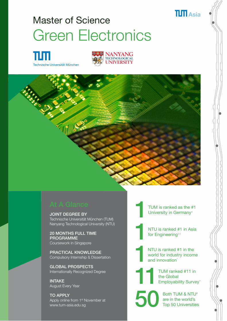
Master of Science
Green Electronics
1111150
At A Glance
JOINT DEGREE BY Technische Universität München (TUM) Nanyang Technological University (NTU)
20 MONTHS FULL TIME PROGRAMMECoursework in Singapore
PRACTICAL KNOWLEDGECompulsory Internship & Dissertation
GLOBAL PROSPECTSInternationally Recognized Degree INTAKE August Every Year
TO APPLY Apply online from 1st November at www.tum-asia.edu.sg
NTU Full Logo printing on uncoated stock: CMYK
0C 100M 90Y 0K 100C 68M 7Y 28K
TUM is ranked as the #1 University in Germany+
NTU is ranked #1 in Asia for Engineering++
TUM ranked #11 in the Global Employability Survey^
Both TUM & NTU# are in the world’s Top 50 Universities
NTU is ranked #1 in the world for industry income and innovation*
02 Technische Universität München Asia - TUM Asia
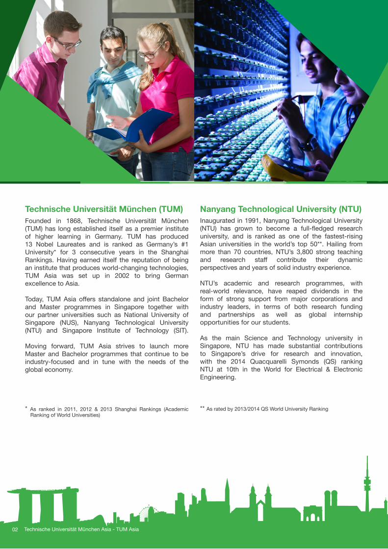
Founded in 1868, Technische Universität München (TUM) has long established itself as a premier institute of higher learning in Germany. TUM has produced 13 Nobel Laureates and is ranked as Germany’s #1 University* for 3 consecutive years in the Shanghai Rankings. Having earned itself the reputation of being an institute that produces world-changing technologies, TUM Asia was set up in 2002 to bring German excellence to Asia. Today, TUM Asia offers standalone and joint Bachelor and Master programmes in Singapore together with our partner universities such as National University of Singapore (NUS), Nanyang Technological University (NTU) and Singapore Institute of Technology (SIT). Moving forward, TUM Asia strives to launch more Master and Bachelor programmes that continue to be industry-focused and in tune with the needs of the global economy.
* As ranked in 2011, 2012 & 2013 Shanghai Rankings (Academic Ranking of World Universities)
Technische Universität München (TUM) Inaugurated in 1991, Nanyang Technological University (NTU) has grown to become a full-fledged research university, and is ranked as one of the fastest-rising Asian universities in the world’s top 50**. Hailing from more than 70 countries, NTU’s 3,800 strong teaching and research staff contribute their dynamic perspectives and years of solid industry experience.
NTU’s academic and research programmes, with real-world relevance, have reaped dividends in the form of strong support from major corporations and industry leaders, in terms of both research funding and partnerships as well as global internship opportunities for our students.
As the main Science and Technology university in Singapore, NTU has made substantial contributions to Singapore’s drive for research and innovation, with the 2014 Quacquarelli Symonds (QS) ranking NTU at 10th in the World for Electrical & Electronic Engineering.
** As rated by 2013/2014 QS World University Ranking
Nanyang Technological University (NTU)
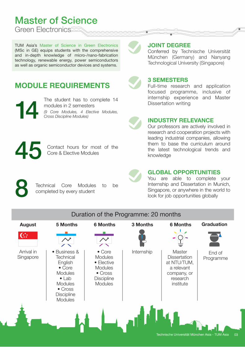
Duration of the Programme: 20 months
Arrival in Singapore
• Business & Technical English• Core
Modules• Lab
Modules• Cross
Discipline Modules
• Core Modules• Elective Modules• Cross
Discipline Modules
Internship Master Dissertation
at NTU/TUM, a relevant
company, or research institute
End of Programme
5 MonthsAugust 6 Months 3 Months 6 Months Graduation
Master of Science Green Electronics
TUM Asia’s Master of Science in Green Electronics (MSc in GE) equips students with the comprehensive and in-depth knowledge of micro-/nano-fabrication technology, renewable energy, power semiconductors as well as organic semiconductor devices and systems.
03Technische Universität München Asia - TUM Asia
JOINT DEGREEConferred by Technische Universität München (Germany) and Nanyang Technological University (Singapore)
3 SEMESTERSFull-time research and application focused programme, inclusive of internship experience and Master Dissertation writing
INDUSTRY RELEVANCE Our professors are actively involved in research and cooperation projects with leading industrial companies, allowing them to base the curriculum around the latest technological trends and knowledge
GLOBAL OPPORTUNITIESYou are able to complete your Internship and Dissertation in Munich, Singapore, or anywhere in the world to look for job opportunities globally
MODULE REQUIREMENTS
845 Contact hours for most of the
Core & Elective Modules
Technical Core Modules to be completed by every student
14 The student has to complete 14 modules in 2 semesters (9 Core Modules, 4 Elective Modules, Cross Discipline Modules)
04 Technische Universität München Asia - TUM Asia
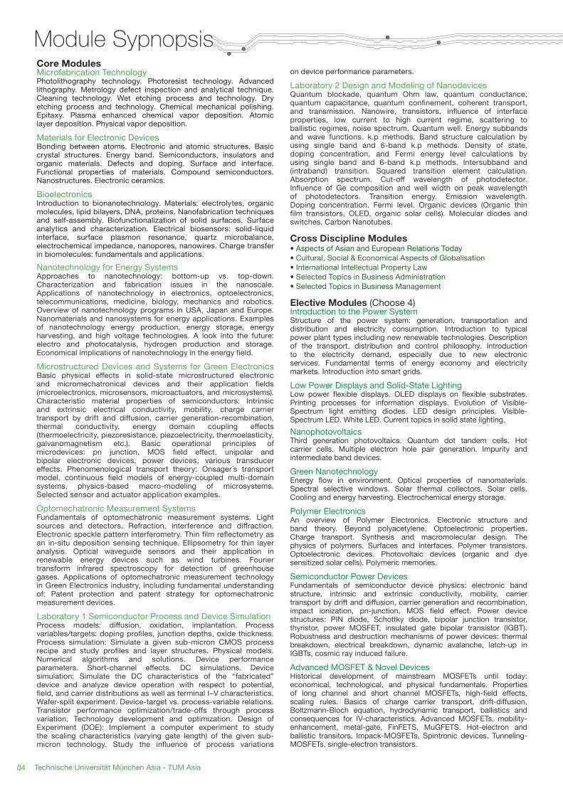
Module Sypnopsis on device performance parameters. Laboratory 2 Design and Modeling of Nanodevices Quantum blockade, quantum Ohm law, quantum conductance, quantum capacitance, quantum confinement, coherent transport, and transmission. Nanowire, transistors, influence of interface properties, low current to high current regime, scattering to ballistic regimes, noise spectrum. Quantum well. Energy subbands and wave functions. k.p methods. Band structure calculation by using single band and 6-band k.p methods. Density of state, doping concentration, and Fermi energy level calculations by using single band and 6-band k.p methods. Intersubband and (intraband) transition. Squared transition element calculation. Absorption spectrum. Cut-off wavelength of photodetector. Influence of Ge composition and well width on peak wavelength of photodetectors. Transition energy. Emission wavelength. Doping concentration. Fermi level. Organic devices (Organic thin film transistors, OLED, organic solar cells). Molecular diodes and switches. Carbon Nanotubes. Cross Discipline Modules• Aspects of Asian and European Relations Today • Cultural, Social & Economical Aspects of Globalisation • International Intellectual Property Law • Selected Topics in Business Administration • Selected Topics in Business Management
Elective Modules (Choose 4)Introduction to the Power SystemStructure of the power system: generation, transportation and distribution and electricity consumption. Introduction to typical power plant types including new renewable technologies. Description of the transport, distribution and control philosophy. Introduction to the electricity demand, especially due to new electronic services. Fundamental terms of energy economy and electricity markets. Introduction into smart grids.
Low Power Displays and Solid-State LightingLow power flexible displays. OLED displays on flexible substrates. Printing processes for information displays. Evolution of Visible- Spectrum light emitting diodes. LED design principles. Visible- Spectrum LED. White LED. Current topics in solid state lighting. NanophotovoltaicsThird generation photovoltaics. Quantum dot tandem cells. Hot carrier cells. Multiple electron hole pair generation. Impurity and intermediate band devices. Green NanotechnologyEnergy flow in environment. Optical properties of nanomaterials. Spectral selective windows. Solar thermal collectors. Solar cells. Cooling and energy harvesting. Electrochemical energy storage. Polymer ElectronicsAn overview of Polymer Electronics. Electronic structure and band theory. Beyond polyacetylene. Optoelectronic properties. Charge transport. Synthesis and macromolecular design. The physics of polymers. Surfaces and interfaces. Polymer transistors. Optoelectronic devices. Photovoltaic devices (organic and dye sensitized solar cells). Polymeric memories.
Semiconductor Power DevicesFundamentals of semiconductor device physics: electronic band structure, intrinsic and extrinsic conductivity, mobility, carrier transport by drift and diffusion, carrier generation and recombination, impact ionization, pn-junction, MOS field effect. Power device structures: PIN diode, Schottky diode, bipolar junction transistor, thyristor, power MOSFET, insulated gate bipolar transistor (IGBT). Robustness and destruction mechanisms of power devices: thermal breakdown, electrical breakdown, dynamic avalanche, latch-up in IGBTs, cosmic ray induced failure.
Advanced MOSFET & Novel DevicesHistorical development of mainstream MOSFETs until today: economical, technological, and physical fundamentals. Properties of long channel and short channel MOSFETs, high-field effects, scaling rules. Basics of charge carrier transport, drift-diffusion, Boltzmann-Bloch equation, hydrodynamic transport, ballistics and consequences for IV-characteristics. Advanced MOSFETs, mobility- enhancement, metal-gate, FinFETS, MuGFETS. Hot-electron and ballistic transitors, Impack-MOSFETs, Spintronic devices. Tunneling- MOSFETs, single-electron transistors.
Core ModulesMicrofabrication TechnologyPhotolithography technology. Photoresist technology. Advanced lithography. Metrology defect inspection and analytical technique. Cleaning technology. Wet etching process and technology. Dry etching process and technology. Chemical mechanical polishing. Epitaxy. Plasma enhanced chemical vapor deposition. Atomic layer deposition. Physical vapor deposition. Materials for Electronic DevicesBonding between atoms. Electronic and atomic structures. Basic crystal structures. Energy band. Semiconductors, insulators and organic materials. Defects and doping. Surface and interface. Functional properties of materials. Compound semiconductors. Nanostructures. Electronic ceramics. BioelectronicsIntroduction to bionanotechnology. Materials: electrolytes, organic molecules, lipid bilayers, DNA, proteins. Nanofabrication techniques and self-assembly. Biofunctionalization of solid surfaces. Surface analytics and characterization. Electrical biosensors: solid-liquid interface, surface plasmon resonance, quartz microbalance, electrochemical impedance, nanopores, nanowires. Charge transfer in biomolecules: fundamentals and applications. Nanotechnology for Energy SystemsApproaches to nanotechnology: bottom-up vs. top-down. Characterization and fabrication issues in the nanoscale. Applications of nanotechnology in electronics, optoelectronics, telecommunications, medicine, biology, mechanics and robotics. Overview of nanotechnology programs in USA, Japan and Europe. Nanomaterials and nanosystems for energy applications. Examples of nanotechnology energy production, energy storage, energy harvesting, and high voltage technologies. A look into the future: electro and photocatalysis, hydrogen production and storage. Economical implications of nanotechnology in the energy field. Microstructured Devices and Systems for Green Electronics Basic physical effects in solid-state microstructured electronic and micromechatronical devices and their application fields (microelectronics, microsensors, microactuators, and microsystems). Characteristic material properties of semiconductors: Intrinsic and extrinsic electrical conductivity, mobility, charge carrier transport by drift and diffusion, carrier generation-recombination, thermal conductivity, energy domain coupling effects (thermoelectricity, piezoresistance, piezoelectricity, thermoelasticity, galvanomagnetism etc.). Basic operational principles of microdevices: pn junction, MOS field effect, unipolar and bipolar electronic devices, power devices, various transducer effects. Phenomenological transport theory: Onsager´s transport model, continuous field models of energy-coupled multi-domain systems, physics-based macro-modeling of microsystems. Selected sensor and actuator application examples.
Optomechatronic Measurement SystemsFundamentals of optomechatronic measurement systems. Light sources and detectors. Refraction, interference and diffraction. Electronic speckle pattern interferometry. Thin film reflectometry as an in-situ deposition sensing technique. Ellipsometry for thin layer analysis. Optical waveguide sensors and their application in renewable energy devices such as wind turbines. Fourier transform infrared spectroscopy for detection of greenhouse gases. Applications of optomechatronic measurement technology in Green Electronics industry, including fundamental understanding of: Patent protection and patent strategy for optomechatronic measurement devices. Laboratory 1 Semiconductor Process and Device SimulationProcess models: diffusion, oxidation, implantation. Process variables/targets: doping profiles, junction depths, oxide thickness. Process simulation: Simulate a given sub-micron CMOS process recipe and study profiles and layer structures. Physical models. Numerical algorithms and solutions. Device performance parameters. Short-channel effects. DC simulations. Device simulation: Simulate the DC characteristics of the “fabricated” device and analyze device operation with respect to potential, field, and carrier distributions as well as terminal I–V characteristics. Wafer-split experiment. Device-target vs. process-variable relations. Transistor performance optimization/trade-offs through process variation. Technology development and optimization. Design of Experiment (DOE): Implement a computer experiment to study the scaling characteristics (varying gate length) of the given sub- micron technology. Study the influence of process variations
Admissions Information
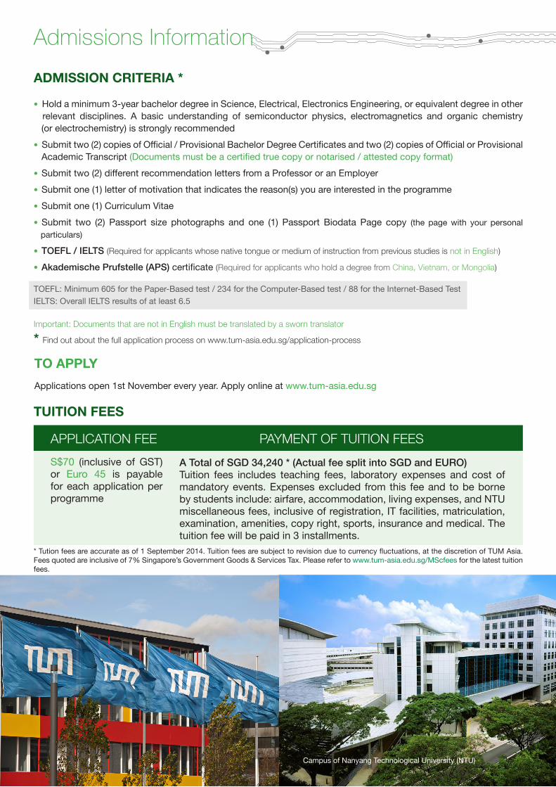
APPLICATION FEE
TUITION FEES
PAYMENT OF TUITION FEESS$70 (inclusive of GST) or Euro 45 is payable for each application per programme
A Total of SGD 34,240 * (Actual fee split into SGD and EURO)Tuition fees includes teaching fees, laboratory expenses and cost of mandatory events. Expenses excluded from this fee and to be borne by students include: airfare, accommodation, living expenses, and NTU miscellaneous fees, inclusive of registration, IT facilities, matriculation, examination, amenities, copy right, sports, insurance and medical. The tuition fee will be paid in 3 installments.
TO APPLYApplications open 1st November every year. Apply online at www.tum-asia.edu.sg
ADMISSION CRITERIA *
• Hold a minimum 3-year bachelor degree in Science, Electrical, Electronics Engineering, or equivalent degree in other relevant disciplines. A basic understanding of semiconductor physics, electromagnetics and organic chemistry (or electrochemistry) is strongly recommended • Submit two (2) copies of Official / Provisional Bachelor Degree Certificates and two (2) copies of Official or Provisional Academic Transcript (Documents must be a certified true copy or notarised / attested copy format)• Submit two (2) different recommendation letters from a Professor or an Employer• Submit one (1) letter of motivation that indicates the reason(s) you are interested in the programme • Submit one (1) Curriculum Vitae• Submit two (2) Passport size photographs and one (1) Passport Biodata Page copy (the page with your personal particulars)
• TOEFL / IELTS (Required for applicants whose native tongue or medium of instruction from previous studies is not in English)
• Akademische Prufstelle (APS) certificate (Required for applicants who hold a degree from China, Vietnam, or Mongolia)
TOEFL: Minimum 605 for the Paper-Based test / 234 for the Computer-Based test / 88 for the Internet-Based Test IELTS: Overall IELTS results of at least 6.5
Important: Documents that are not in English must be translated by a sworn translator
* Find out about the full application process on www.tum-asia.edu.sg/application-process
* Tution fees are accurate as of 1 September 2014. Tuition fees are subject to revision due to currency fluctuations, at the discretion of TUM Asia. Fees quoted are inclusive of 7% Singapore’s Government Goods & Services Tax. Please refer to www.tum-asia.edu.sg/MScfees for the latest tuition fees.
Campus of Nanyang Technological University (NTU)
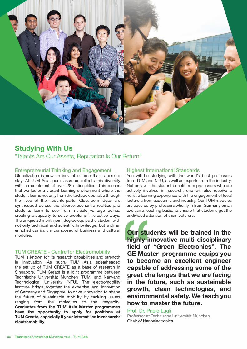
Entrepreneurial Thinking and EngagementGlobalization is now an inevitable force that is here to stay. At TUM Asia, our classroom reflects this diversity with an enrolment of over 28 nationalities. This means that we foster a vibrant learning environment where the student learns not only from the textbook but also through the lives of their counterparts. Classroom ideas are synthesized across the diverse economic realities and students learn to see from multiple vantage points, creating a capacity to solve problems in creative ways. The unique 20 month joint degree equips the student with not only technical and scientific knowledge, but with an enriched curriculum composed of business and cultural modules.
Studying With Us “Talents Are Our Assets, Reputation Is Our Return”
Highest International StandardsYou will be studying with the world’s best professors from TUM and NTU, as well as experts from the industry. Not only will the student benefit from professors who are actively involved in research, one will also receive a holistic learning experience with the engagement of local lecturers from academia and industry. Our TUM modules are covered by professors who fly in from Germany on an exclusive teaching basis, to ensure that students get the undivided attention of their lecturers.
06 Technische Universität München Asia - TUM Asia
TUM CREATE - Centre for Electromobility TUM is known for its research capabilities and strength in innovation. As such, TUM Asia spearheaded the set up of TUM CREATE as a base of research in Singapore. TUM Create is a joint programme between Technische Universität München (TUM) and Nanyang Technological University (NTU). The electromobility institute brings together the expertise and innovation of Germany and Singapore, to drive innovation to shape the future of sustainable mobility by tackling issues ranging from the molecues to the megacity. Graduates from the TUM Asia Master programmes have the opportunity to apply for positions at TUM Create, especially if your interest lies in research/electromobility.
“Prof. Dr. Paolo LugliProfessor at Technische Universität München, Chair of Nanoelectronics
Our students will be trained in the highly innovative multi-disciplinary field of “Green Electronics”. The GE Master programme equips you to become an excellent engineer capable of addressing some of the great challenges that we are facing in the future, such as sustainable growth, clean technologies, and environmental safety. We teach you how to master the future.
Singapore is home to approximately 20 semiconductor assembly and test operations
07Technische Universität München Asia - TUM Asia
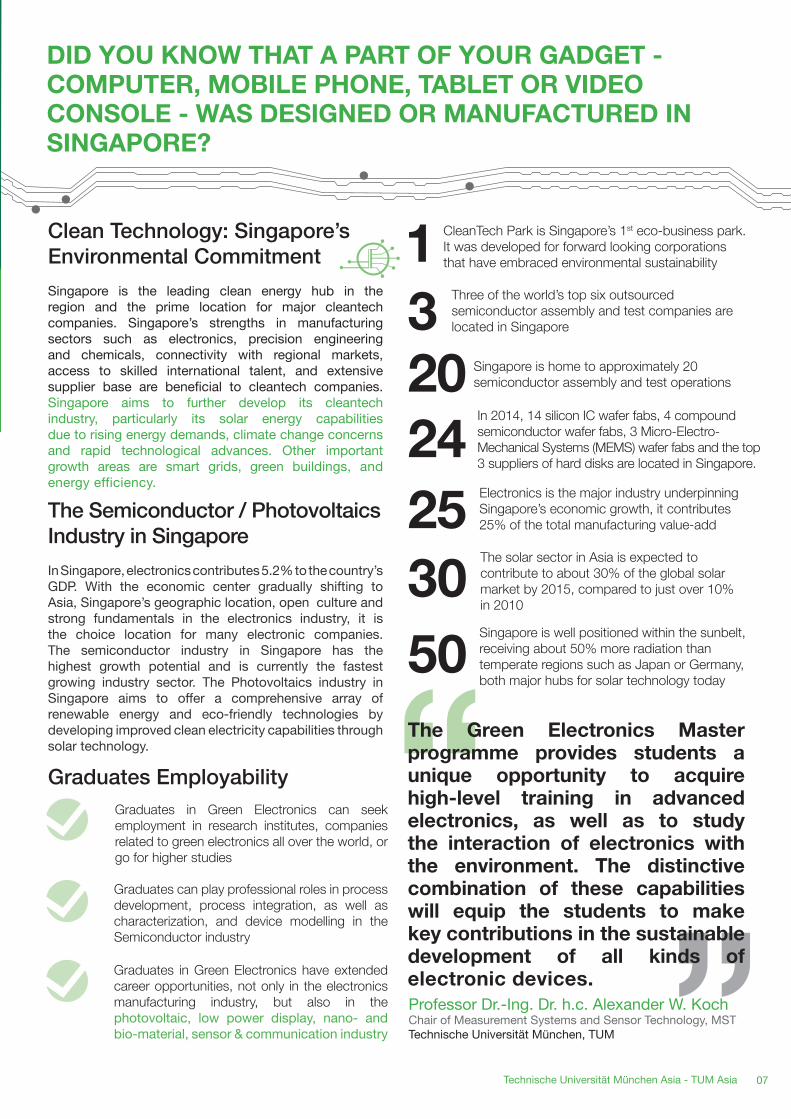
DID YOU KNOW THAT A PART OF YOUR GADGET - COMPUTER, MOBILE PHONE, TABLET OR VIDEO CONSOLE - WAS DESIGNED OR MANUFACTURED IN SINGAPORE?
Clean Technology: Singapore’s Environmental CommitmentSingapore is the leading clean energy hub in the region and the prime location for major cleantech companies. Singapore’s strengths in manufacturing sectors such as electronics, precision engineering and chemicals, connectivity with regional markets, access to skilled international talent, and extensive supplier base are beneficial to cleantech companies. Singapore aims to further develop its cleantech industry, particularly its solar energy capabilities due to rising energy demands, climate change concerns and rapid technological advances. Other important growth areas are smart grids, green buildings, and energy efficiency.
CleanTech Park is Singapore’s 1st eco-business park. It was developed for forward looking corporations that have embraced environmental sustainability
Electronics is the major industry underpinning Singapore’s economic growth, it contributes 25% of the total manufacturing value-add
In 2014, 14 silicon IC wafer fabs, 4 compound semiconductor wafer fabs, 3 Micro-Electro- Mechanical Systems (MEMS) wafer fabs and the top 3 suppliers of hard disks are located in Singapore.
The Semiconductor / Photovoltaics Industry in SingaporeIn Singapore, electronics contributes 5.2% to the country’s GDP. With the economic center gradually shifting to Asia, Singapore’s geographic location, open culture and strong fundamentals in the electronics industry, it is the choice location for many electronic companies. The semiconductor industry in Singapore has the highest growth potential and is currently the fastest growing industry sector. The Photovoltaics industry in Singapore aims to offer a comprehensive array of renewable energy and eco-friendly technologies by developing improved clean electricity capabilities through solar technology.
Graduates Employability
1
The solar sector in Asia is expected to contribute to about 30% of the global solar market by 2015, compared to just over 10% in 2010
3 Three of the world’s top six outsourced semiconductor assembly and test companies are located in Singapore
20242530
Graduates in Green Electronics can seek employment in research institutes, companies related to green electronics all over the world, or go for higher studies
Graduates can play professional roles in process development, process integration, as well as characterization, and device modelling in the Semiconductor industry
“ “The Green Electronics Master programme provides students a unique opportunity to acquire high-level training in advanced electronics, as well as to study the interaction of electronics with the environment. The distinctive combination of these capabilities will equip the students to make key contributions in the sustainable development of all kinds of electronic devices.Graduates in Green Electronics have extended
career opportunities, not only in the electronics manufacturing industry, but also in the photovoltaic, low power display, nano- and bio-material, sensor & communication industry
50 Singapore is well positioned within the sunbelt, receiving about 50% more radiation than temperate regions such as Japan or Germany, both major hubs for solar technology today
Professor Dr.-Ing. Dr. h.c. Alexander W. KochChair of Measurement Systems and Sensor Technology, MSTTechnische Universität München, TUM
German Institute of Science & Technology - TUM Asia 10 Central Exchange Green #03-01 Pixel Building Singapore 138649 Tel: +65 6777 7407 / +49 89 416 177428 Fax: +65 6777 7236 Email: [email protected] www.tum-asia.edu.sg
German Institute of Science & Technology - TUM AsiaCPE Registration No.: 200105229R CPE Registered Period: 13/06/2011 to 12/06/2017 All information is accurate at time of printing and subjected to change. Printed September 2014.
+ As rated by Academic Ranking of World Universities (Shanghai Ranking) 2011, 2012 and 2013 and 2012/2013 QS World University Ranking++ As rated by Academic Ranking of World Universities (Shanghai Ranking) 2014* As rated by the Times Higher Education University Ranking 2013/2014^ As ranked in the 2013 Global Employability Survey by The New York Times# As ranked by Academic Ranking of World Universities (Shanghai Ranking) 2013 and 2013/2014 QS World University Ranking