Manual EVB Mint Module MB86277 Version PA 04.1 January …€¦ · Preliminary 1(18) Prepared...
18
Preliminary 1(18) Prepared Document Number Manfred Ortmann Approved Checked Date Revision Storage Manfred Ortmann 2008-01-23 PA4.1 Mycable01 Receiver: EVB Mint users Info: Manual EVB Mint Module MB86277 Version PA 04.1 January 23, 2008 http://www.fujitsu.com/emea/services/microelectronics FUJITSU PROPRIETARY AND CONFIDENTIAL
-
Upload
phungtuong -
Category
Documents
-
view
218 -
download
3
Transcript of Manual EVB Mint Module MB86277 Version PA 04.1 January …€¦ · Preliminary 1(18) Prepared...
Preliminary1(18)
Prepared Document Number
Manfred OrtmannApproved Checked Date Revision Storage
Manfred Ortmann 2008-01-23 PA4.1 Mycable01
Receiver:
EVB Mint users
Info:
Manual
EVB Mint Module
MB86277
Version PA 04.1 January 23, 2008
http://www.fujitsu.com/emea/services/microelectronics
FUJITSU PROPRIETARY AND CONFIDENTIAL
Preliminary2(18)
Prepared Document Number
Manfred OrtmannApproved Checked Date Revision Storage
Manfred Ortmann 2008-01-23 PA4.1 Mycable01
FUJITSU PROPRIETARY AND CONFIDENTIAL
Preliminary3(18)
Prepared Document Number
Manfred OrtmannApproved Checked Date Revision Storage
Manfred Ortmann 2008-01-23 PA4.1 Mycable01
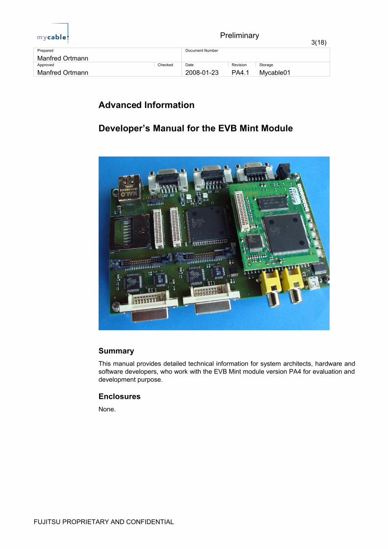
Advanced Information
Developer’s Manual for the EVB Mint Module
SummaryThis manual provides detailed technical information for system architects, hardware and software developers, who work with the EVB Mint module version PA4 for evaluation and development purpose.
EnclosuresNone.
FUJITSU PROPRIETARY AND CONFIDENTIAL

Preliminary4(18)
Prepared Document Number
Manfred OrtmannApproved Checked Date Revision Storage
Manfred Ortmann 2008-01-23 PA4.1 Mycable01
Product InformationProduct InformationThe EVB Mint is a module based on Fujitsu’s MB86277 also called MINT.
The MINT has following features:
● CMOS 0.18µm technology
● Internal and memory frequency : 100MHz ( generated by on-chip PLL )
● Base-clock for display clocks : 400.9MHz ( generated by on-chip PLL )
● Display resolutions typically from 320x234 up to 1024x768
● 6 layers of overlay display ( windows )
● Alpha Plane and constant alpha value for each layer
● Digital Video input ( various formats including YUV )
● Video Scaler ( down scaling )
● RGB digital output ( 8bit x 3 )
● RGB Analog Output
● Built-in alpha blending, anti-aliasing and chroma-keying
● Rendering Engine for various kinds of 2D graphic acceleration functions
● Texture Mapping Unit for 2D polygon support up to 4096x4096 textures
● Bit-Blt Unit for transfers up to 4096x4096 areas
● Alpha Bit-Blt and ROP2 functions
● External 32-bit SDRAM interface for up to 64MB graphic memory
● Parallel host interface ( FR,SH3,SH4,V850,SparcLite etc )
● Internal and external DMA support
● I2C Master interface
● Supply voltage 3.3V ( I/O ), 1.8V ( Internal )
● LQFP-256 Package
● Typical power consumption < 1.0W ( estimated )
● Temperature range -40..+85 °C
Further information about the MINT can be obtained from the datasheet.
The module is designed to plug it on the 467 GDC board.
FUJITSU PROPRIETARY AND CONFIDENTIAL

Preliminary5(18)
Prepared Document Number
Manfred OrtmannApproved Checked Date Revision Storage
Manfred Ortmann 2008-01-23 PA4.1 Mycable01
Revision History
Version Date Sign DescriptionPA 4.1 2007-11-23 mo Create this document
Contact Information
mycable GmbHMichael Carstens-Behrens( hardware and commercial )
Email [email protected]
Tel. +49 4321 55956 55
FUJITSU PROPRIETARY AND CONFIDENTIAL

Preliminary6(18)
Prepared Document Number
Manfred OrtmannApproved Checked Date Revision Storage
Manfred Ortmann 2008-01-23 PA4.1 Mycable01
Table of Contents
1 OVERVIEW.................................................................................................................... 71.1 MANUAL SCOPE............................................................................................................ 71.2 PUTTING INTO OPERATION............................................................................................... 7
2 EVB MINT MODULE...................................................................................................... 82.1 FEATURES................................................................................................................... 82.2 SYSTEM ARCHITECTURE.................................................................................................. 82.3 FUNCTION UNITS......................................................................................................... 11
2.3.1Power Supply................................................................................................... 112.3.2Reset ............................................................................................................... 112.3.3Host CPU Interface.......................................................................................... 112.3.4SDRAM............................................................................................................ 132.3.5Video Output.................................................................................................... 132.3.6Video Input....................................................................................................... 14
2.4 HARDWARE VARIANTS.................................................................................................. 142.5 PLACEMENT OF COMPONENTS........................................................................................ 152.6 MECHANICAL DIMENSIONS............................................................................................. 17
FUJITSU PROPRIETARY AND CONFIDENTIAL
Preliminary7(18)
Prepared Document Number
Manfred OrtmannApproved Checked Date Revision Storage
Manfred Ortmann 2008-01-23 PA4.1 Mycable01
1 Overview
1.1 Manual Scope
This manual provides detailed technical information about the EVB Mint module for system architects, hardware and software developers covering:
● System architecture description and users manual
● Hardware architecture
● Mechanical information
● References to further information like design data, data sheets, software documentation
It is the engineer’s reference for evaluation, system development and prototyping based on the module. This document covers all available hardware versions regarding their configuration options and revision state.
1.2 Putting into Operation
Plug the EVB Mint on a board only if the power supply is off !
FUJITSU PROPRIETARY AND CONFIDENTIAL

Preliminary8(18)
Prepared Document Number
Manfred OrtmannApproved Checked Date Revision Storage
Manfred Ortmann 2008-01-23 PA4.1 Mycable01
2 EVB Mint Module
2.1 Features
The EVB Mint module has the following features:
• MINT ( MB86277 )
• SDRAM
• Needs 3.3 V DC power supply only
• Plugable with three connectors on 467 GDC board
• Card size 75.0 x 60.0 mm
• Operating temperature range -40 ... + 85 Grad Celsius
2.2 System Architecture
The system architecture of the EVB Mint module is shown in picture 2-1.
Pic. 2-1: EVB Mint module block diagram
FUJITSU PROPRIETARY AND CONFIDENTIAL

Preliminary9(18)
Prepared Document Number
Manfred OrtmannApproved Checked Date Revision Storage
Manfred Ortmann 2008-01-23 PA4.1 Mycable01
Picture 2-2 shows the top side of the EVB Mint module, Picture 2-3 shows the bottom side.
Pic. 2-2: EVB Mint module top side
FUJITSU PROPRIETARY AND CONFIDENTIAL

Preliminary10(18)
Prepared Document Number
Manfred OrtmannApproved Checked Date Revision Storage
Manfred Ortmann 2008-01-23 PA4.1 Mycable01
Pic. 2-3: EVB Mint module bottom side
FUJITSU PROPRIETARY AND CONFIDENTIAL
Preliminary11(18)
Prepared Document Number
Manfred OrtmannApproved Checked Date Revision Storage
Manfred Ortmann 2008-01-23 PA4.1 Mycable01
2.3 Function Units
2.3.1 Power SupplyThe modul needs only 3.3 V DC for power supply.
1.8 V for the MINT will be regulated from the switching regulator LTC3411 ( U100 ) from Linear Technologies on the modul.
2.3.2 Reset The microprocessor reset circuit LM3724 from National Semiconductors ( U101 ) generates a power on reset.
An external reset can be asserted through a reset input at the host CPU extension interface ( RESET#0 ).
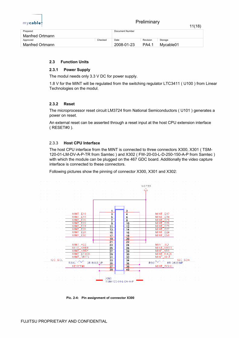
2.3.3 Host CPU InterfaceThe host CPU interface from the MINT is connected to three connectors X300, X301 ( TSM-120-01-LM-DV-A-P-TR from Samtec ) and X302 ( FW-20-03-L-D-250-150-A-P from Samtec )with which the module can be plugged on the 467 GDC board. Additionally the video capture interface is connected to these connectors.
Following pictures show the pinning of connector X300, X301 and X302:
Pic. 2-4: Pin assignment of connector X300
FUJITSU PROPRIETARY AND CONFIDENTIAL

Preliminary12(18)
Prepared Document Number
Manfred OrtmannApproved Checked Date Revision Storage
Manfred Ortmann 2008-01-23 PA4.1 Mycable01
Pic. 2-5: Pin assignment of connector X301
Pic. 2-6: Pin assignment of connector X302
FUJITSU PROPRIETARY AND CONFIDENTIAL

Preliminary13(18)
Prepared Document Number
Manfred OrtmannApproved Checked Date Revision Storage
Manfred Ortmann 2008-01-23 PA4.1 Mycable01
The configuration pins of the MINT are strapped on the board by 10k resistors to VCC. By populating a 0 Ohm resistor the corresponding pin can be tied to GND.
Following table shows which resistor is assigned to tie the pin to low.
Pin name Pull down
resistorDefault
PopulationCLKSEL0 R419 noCLKSEL1 R418 yesRDY_MODE R417 yesBS_MODE R416 yesMODE0 R415 yesMODE1 R414 yesDRACK R413 noDTACK R409 noXRDY R408 noXBS R406 no
So as default following options are adjusted: 32 bit demux, no BS signal used and normal not ready.
The 14.32 MHz CLK signal for the MINT will be generated on the module by the oscillator U400( SG8002CE from Epson ).
2.3.4 SDRAMThe modul is populated with two 256 MBit SDRAM ( MT48LC16M16A2TG-75-IT ) from Micron ( U500, U501 ) as graphic memory.
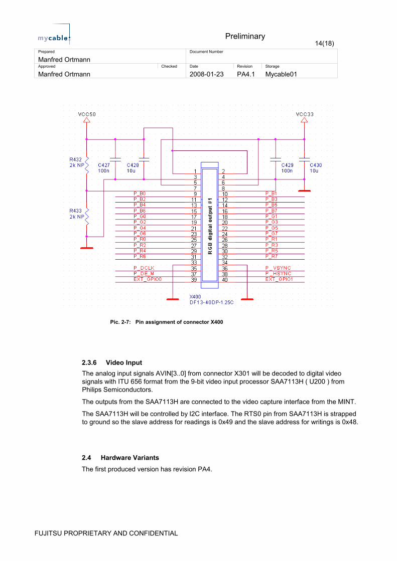
2.3.5 Video OutputThe video output interface from the MINT is connected to connector X400 ( DF13-40-DP-1.25V(55) from Hirose ) on the top side.
It is forseen to connect this interface with the 467 GDC board by a cable.
Following pictures show the pinning of connector X400:
FUJITSU PROPRIETARY AND CONFIDENTIAL
Preliminary14(18)
Prepared Document Number
Manfred OrtmannApproved Checked Date Revision Storage
Manfred Ortmann 2008-01-23 PA4.1 Mycable01
Pic. 2-7: Pin assignment of connector X400
2.3.6 Video InputThe analog input signals AVIN[3..0] from connector X301 will be decoded to digital video signals with ITU 656 format from the 9-bit video input processor SAA7113H ( U200 ) from Philips Semiconductors.
The outputs from the SAA7113H are connected to the video capture interface from the MINT.
The SAA7113H will be controlled by I2C interface. The RTS0 pin from SAA7113H is strapped to ground so the slave address for readings is 0x49 and the slave address for writings is 0x48.
2.4 Hardware VariantsThe first produced version has revision PA4.
FUJITSU PROPRIETARY AND CONFIDENTIAL

Preliminary15(18)
Prepared Document Number
Manfred OrtmannApproved Checked Date Revision Storage
Manfred Ortmann 2008-01-23 PA4.1 Mycable01
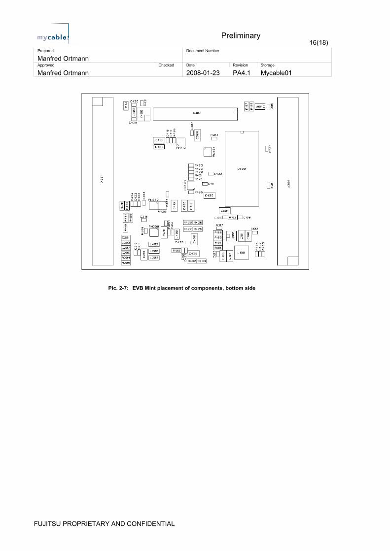
2.5 Placement of Components
The placement of components on the EVB Mint Module is shown below.
Pic. 2-6: EVB Mint placement of components, top side
FUJITSU PROPRIETARY AND CONFIDENTIAL
Preliminary16(18)
Prepared Document Number
Manfred OrtmannApproved Checked Date Revision Storage
Manfred Ortmann 2008-01-23 PA4.1 Mycable01
Pic. 2-7: EVB Mint placement of components, bottom side
FUJITSU PROPRIETARY AND CONFIDENTIAL

Preliminary17(18)
Prepared Document Number
Manfred OrtmannApproved Checked Date Revision Storage
Manfred Ortmann 2008-01-23 PA4.1 Mycable01
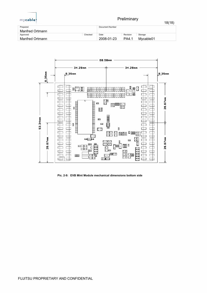
2.6 Mechanical Dimensions
The EVB Mint module has a card size of 68.6 x 53.3 mm.
Pic. 2-8: EVB Mint Module mechanical dimensions top side
FUJITSU PROPRIETARY AND CONFIDENTIAL
Preliminary18(18)
Prepared Document Number
Manfred OrtmannApproved Checked Date Revision Storage
Manfred Ortmann 2008-01-23 PA4.1 Mycable01
Pic. 2-9: EVB Mint Module mechanical dimensions bottom side
FUJITSU PROPRIETARY AND CONFIDENTIAL