Optical manipulation of a single human virus for study of ...

Manipulation of
Single Atoms
Ajit Gopalakrishnan (CH04B055)
K B Ganesh (BT04B015)
Pavan Srinath (BT04B051)
Radha Ramachandran (CH04B034)
Vinod Kumar V (CH04B046)

Manipulation of Single Atoms
Introduction to ‘Atom manipulation’
We have seen a surge of development in the field of Nanotechnology these past
two decades or so. There is now a need to build nanoscale structures that,
wherein one needs to engineer groups of atoms and molecules in required
fashion. Building structures and devices at this level is quite different from
everything else, and one needs to start afresh. To fulfill this dream, a good way
to go is to use a bottom‐up approach, starting from atoms and molecules. To do
this, we need to learn how to manipulate single atoms.
Eigler DM and Schweizer EK in 1990 were able to construct a structure made of
single atoms, by manipulating them in a controlled fashion. Their achievement
sparked off the manipulation of single atoms and molecules.
In this report, we will be analyzing the major techniques used for atom
manipulation, namely low temperature Scanning Tunneling Microscopy and
Atomic Force Microscopy. We shall start with STM and how manipulation using
the techniques was developed. After that, we will go into the finer details and
look at the various modes of manipulation; all illustrated with case studies. After
that, we will discuss manipulation using AFM, which has been done only since
recently. In the end, we will also take a brief look at Optical manipulation.
- 2 -

Manipulation of Single Atoms
1. Scanning Tunneling Microscopy STM was built and used first by Binnig, Rohrer et al. [1], [2] in 1983. It was a
device constructed to facilitate surface studies at a nanometer‐level. Instead of employing optical methods of microscopy, STM uses the quantum mechanical phenomenon of vacuum tunneling for the imaging. An atomically sharp probe (the tip) is moved over the surface of the material under study, and a voltage is applied between probe and the surface. Depending on the voltage, electrons will ʺtunnelʺ or jump from the tip to the surface (or vice‐versa, depending on the polarity), resulting in a weak electric current. The size of this tunnel current is exponentially dependent on the distance between probe and the surface. For tunneling to occur, the substrate being scanned must be conductive (or semiconductive). The primary drawback of STM is that insulators cannot be scanned through the technique, as the electron has no available energy state to tunnel into or out of due to the band gap structure in insulators.
Figure 1. Schematic picture of the STM scanner. Mounted in the center of the base plate is the piezoelectric tube scanner holding the tip. On the outside are the three tube scanners used for coarse approach. A temperature sensor and a small resistance heater are mounted on the thick copper sample. [3]
- 3 -

Manipulation of Single Atoms
Figure 2. Schematic view of an STM. Creative Commons
The position and the motion of the tip are controlled by placing various
voltages on the electrodes of a piezoelectric element.
The microscopy can be done in two modes:
• A constant current mode where a feedback loop keeps the tunneling current constant by adjusting the distance between the tip and the surface. By scanning the tip over the surface and measuring the height (which is directly related to the voltage applied to the piezo‐element), one can thus reconstruct the surface structure of the material under study.
• A constant height mode where the scan is made at a constant height above the surface, and the varying current is noted.
2. Development of Manipulation using STM Investigations using the STM were usually done at room temperature, but there
were developments made to work at low temperatures ranging down to 4 K. Later, it was found that not only surface‐scanning, but that surface‐modification was also possible using STM.[4] The breakthrough for single atom manipulation came when Eigler et al., [5]
were able to position single Xenon atoms across a single‐crystal Nickel (110) surface, using STM at 4 K, in an ultra‐high‐vacuum. The tip in an STM always exerts a finite force on the surface atoms (from Van der Waals and electrostatic
- 4 -

Manipulation of Single Atoms
contributions). Whilst scanning, this force is sufficient to displace neither the native substrate atoms nor atoms adsorbed onto the surface (adatoms). However, if the tip is taken closer, the interaction can become large enough to move some atoms across the surface. Here, the surface was first scanned. The interaction was too low (10‐9 A at 0.01 V) to perturb the atoms out of their place. The tip was then placed directly over a Xe atom and lowered, till the current increased to around 1.8x10‐8 A. Now, the atom was bound to the tip, and could move with it along the surface. It is important to note that the Xenon atom here never loses contact with the metal surface. It was dragged till the point of interest, and then the tip was retracted. A second scan is always done after manipulation to find out where the atom now was shifted to. The letters ‘I B M’ were drawn this way.
Figure 3. A sequence of STM images taken during the construction of a patterned array of Xenon atoms on a Nickel (110) surface. Each letter is 5 nm from top to bottom. [5]
Using the same technique, a simple linear multimer was created, as illustrated
below. This breakthrough shifted the focus of STM from pure imaging to the manipulation of atoms and molecules across a surface. However, it took some time before anyone other than the afore‐mentioned group could successfully carry out the manipulation of single atoms in a controlled fashion.
- 5 -

Manipulation of Single Atoms
Eigler and collaborators did not wait to come out with new results, such as their famous construction of a ‘quantum corral’ [6]. In this, they arranged atoms on the
Figure 4. Various steps in the construction of a linear multimer of Xenon atoms on a Nickel (110) surface. The rows of alternating dark and bright lines are the native Nickel atoms of the surface. The distance between the Xe atoms is 5 Å. [5]
surface next to each other in a circular fashion. The scan afterwards showed that there were standing electron waves formed inside the corral. The experimental data found confirm with the quantum mechanical predictions of particles trapped in a 2‐dimensional box [5].
Figure 5. Spatial image of the eigen states of a quantum corral. A 48‐atom Fe‐ring constructed on the Cu (111) surface. Average diameter of ring (atom center to atom center) is 142.6 Å. [6]
Today, the focus has gone beyond single atoms, and developments are being
made in the manipulation of molecules and macromolecules, but we will discuss mainly regarding atoms here. 3. Low Temperature STM Atom manipulation is always done under low temperature and ultra‐high‐
vacuum conditions. At room temperature, the thermal energy of the adatoms is so high that their positions on the substrate do not remain fixed. Initial
- 6 -

Manipulation of Single Atoms
experiments were conducted at 4 K, and later technology was developed to increase the temperature to values like 30K [7] and 60K for certain experiments. Ultra‐high‐vacuum is required to prevent contamination of the surface due to the adsorption of gas‐phase atoms and molecules. Also, at these low temperatures, the system is very stable, which allows one to conduct experiments for many days, after preparing one sample. Essentially, there are two broad types of manipulation were developed based
on STM, namely Lateral and Vertical manipulation. 4. Lateral Manipulation Lateral Manipulation (LM) is done such that the atoms being manipulated
never leave the surface. That is, the bonds between them and the surface are not broken. An extremely fine control over the tip‐atom‐surface interaction is necessary to achieve the atomic scale precision. A typical LM procedure involves three steps: (1) Vertically approaching the tip toward the manipulated atom to increase the tip–atom interaction, (2) Scanning the tip parallel to the surface where the atom moves under the influence of the tip, (3) Retracting the tip back to the normal image height thereby leaving the atom at the final location on the surface. The scanning height is usually around 6‐7 Å. For manipulation, the current is
increased by about two orders of magnitude. This results in reducing the tip‐sample separation by about 3.5‐4.5 Å. [8] If operating in constant current mode, the current value is fixed at this for manipulation, and if the mode is constant height, the tip will be fixed at the new height obtained. Usually, the tips used for lateral manipulation are made of the same atoms as
the native substrate. So, even if the tip is made by etching Tungsten, in situ preparation of the tip is done afterwards such that the tip is covered with the same atoms. The methods for manipulating the adspecies on the surface depend on the nature of the interactions between them and the tip. If the adspecies is repulsed by the tip, then it cannot be manipulated in the same way as an adspecies which is attracted by the tip.
- 7 -

Manipulation of Single Atoms
Figure 6. Working steps for lateral manipulation.
4.1 Threshold tunneling resistance In LM, tunneling resistance (RT) is used to denote the tip‐atom distance, and to
qualitatively estimate the tip‐atom interaction strength [9]. The minimum tip‐atom distance required for a manipulation can be determined by measuring a threshold tunneling current (IT) to move an atom at a fixed bias (Fig. 7 (a)). Fig. 7 (b) shows a plot of IT as a function of applied bias. Here, each data point is determined by plotting a curve, like the one shown in Fig. 7 (a). From the slope of this curve, a threshold tunneling resistance required to move the atom can be determined.
Figure 7. a) Probability to move an atom vs. tunneling current at −45 mV. b) At the small bias range, the threshold current linearly varies with the bias. Rt can be determined from the slope of this curve. [9]
- 8 -

Manipulation of Single Atoms
4.2 Modes of lateral manipulation Based on the nature of the interaction between the tip and the atom, there are
three different LM modes, namely “pulling”, “pushing” and “sliding”.
• Pulling In the pulling mode, the atom follows the tip. This occurs when the forces between the tip and the adatom are attractive in nature. The motion of the adatom is discontinuous. It hops on the surface.
• Pushing In the pushing mode, the atom leads the tip. It occurs when the tip sample forces are repulsive in nature. The motion of the adatom here is again discontinuous and it hops over the other surface atoms.
• Sliding In the sliding mode, the adatom attracted by the tip gradually slides along the surface. When the tip is really close to the sample, the atom is virtually bound to or trapped under the tip and it moves smoothly across the surface together with the tip.
One thing to be noted is that if an atom is attracted to the tip, then it appears as a ‘hill’ on the STM image and that it appears as a depression when it is repulsed by the tip. 4.3 Tip motion in lateral manipulation A schematic diagram of force components involved in an atom manipulation
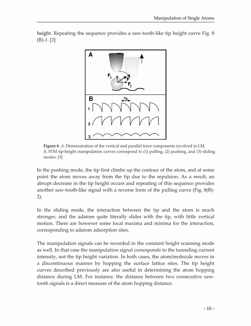
process is illustrated in Fig. 8(a). Here, the STM is set in the constant current scanning mode. The tip is initially located directly above the atom and hence, only a vertical force component FN exists. In pulling mode, the tip‐atom distance is carefully chosen so that the attractive interaction between them is not strong enough to overcome the desorption barrier of the atom. Since the lateral force component FL is negligible at this point the atom will neither transfer to the tip nor move to the next adsorption site (ad‐site) on the surface. When the tip moves parallel to the surface it passes over the manipulated atom, thereby tracing a part of the atomic contour. This action increases FL and decreases FN. When FL overcomes the hopping barrier of the atom, the atom hops to the next ad‐site under the tip. This action alerts the STM feedback system to retract the tip in order to maintain the current constant causing an abrupt increase in the tip
- 9 -
Manipulation of Single Atoms
height. Repeating the sequence provides a saw‐tooth‐like tip height curve Fig. 8 (B)‐1. [3]
Figure 8. A. Demonstration of the vertical and parallel force components involved in LM. B. STM tip‐height manipulation curves correspond to (1) pulling, (2) pushing, and (3) sliding modes. [3]
In the pushing mode, the tip first climbs up the contour of the atom, and at some point the atom moves away from the tip due to the repulsion. As a result, an abrupt decrease in the tip height occurs and repeating of this sequence provides another saw‐tooth‐like signal with a reverse form of the pulling curve (Fig. 8(B)‐2).
In the sliding mode, the interaction between the tip and the atom is much stronger, and the adatom quite literally slides with the tip, with little vertical motion. There are however some local maxima and minima for the interaction, corresponding to adatom adsorption sites.
The manipulation signals can be recorded in the constant height scanning mode as well. In that case the manipulation signal corresponds to the tunneling current intensity, not the tip height variation. In both cases, the atom/molecule moves in a discontinuous manner by hopping the surface lattice sites. The tip height curves described previously are also useful in determining the atom hopping distance during LM. For instance, the distance between two consecutive saw‐tooth signals is a direct measure of the atom hopping distance.
- 10 -

Manipulation of Single Atoms
The LM modes described previously are mostly observed when an atom is manipulated along a close‐packed row direction (a [110] direction) on face‐centered‐cubic (fcc) [111] surfaces. Atoms usually prefer to travel along close‐packed directions on these surfaces due to a lower diffusion barrier as compared to other surface directions. Sophisticated atom movement mechanisms occur when the atom is manipulated along the directions away from the surface close‐packed directions. 4.4 Case Study One can elaborate further on Lateral Manipulation of adspecies, on a Cu (211) surface, by considering some examples from Bartel et al. [9] Cu [211] is a stepped, or a ridged surface. Hence, most adatoms are confined to one ridge, and can be manipulated only up or down a direction.
Figure 9. The anisotropic surface of Cu [211] [9]
i. Cu on Cu [211]
The Cu adatom here will typically move by pulling [9]. Figure 10(a) shows the tip height during moving a Cu atom. In the initial flat part the tip approaches the Cu atom. The following sudden upward jump of the tip must be interpreted as the Cu adatom being attracted by the tip and hence hopping by one adsorption site towards the tip. After this jump the tip moves over the top and then downward along the contour of the Cu adatom. From the contour line of the Cu atom we can deduce that its new location is an fcc adatom site again. Once the downward movement of the tip along the side of the atom has reached a threshold depending on the tunneling resistance, another upward jump of the tip occurs [the second in Fig. 10(a)]. At this point the Cu atom hops by one adsorption site, following the tip.
- 11 -

Manipulation of Single Atoms
ii. Pb on Cu [211]
At a high tunnel resistance like 120 kΩ, Pb behaves just like Cu, (Fig. 9(b)) and hops between adjacent fcc sites [9]. However, Pb is a much bigger atom compared to Cu. Which means that it doesn’t sit as well as Cu in those fcc sites. When the resistance is lowered to a value like 43 kΩ, one finds that the Pb atom moves with the tip in a smoothly and without discontinuities, and little vertical displacement. This is typically characteristic of sliding.
iii. CO on Cu [211]
CO is a molecule which is repulsed by the Cu tip used for manipulation [9]. Even when scanned, the CO molecule appears as a sombrero, as a small hill in a depression (Fig. 9(d)) Usually, controlled manipulation of CO can only be done by using attractive forces. But due to the high anisotropy of the Cu [211], one can use repulsive forces to move the CO molecule. The manipulation is characteristic of pushing.
- 12 -
Figure 10. The left part shows tip height curves during manipulation of a Cu atom, a Pb atom, a CO molecule and a Pb dimer along [110]. The tip movement is from left to right, and the tunneling resistances are indicated. All tip height curves are unfiltered raw data. The vertical dotted lines correspond to fcc sites next to the step edge. On the right part STM images of the different adparticles are shown. [9]

Manipulation of Single Atoms
iv. Pb‐dimer on Cu [211]
We see something very interesting when we take up the case of the Pb‐dimer [9]. Hops by more than one adsorption site can be observed for Pb dimers and even larger Pb clusters. Manipulated by pulling, it moves quite like the single Pb atom at a low resistance like 100 kΩ. However, when the resistance is lowered to 130 kΩ, the dimer performs double hops, and at 190 kΩ, it even performs triple hops. (Fig. 9(e)‐(g)).
5. Vertical Manipulation using STM Vertical Manipulation is the reversible transfer of atoms/molecules between the surface and the STM tip employing additionally electronic/vibrational excitation of the adsorbate by inelastic tunneling. In general, it is more difficult than lateral manipulation as the activation energy barriers needed to lift the adatom from surface maybe substantially higher than in lateral manipulation. Studies have shown that as the tip is brought closer to the surface, the energy barrier decreases and finally vanishes at a certain tip‐substrate distance and the adatom can be pulled to the tip.(Ref. graph below) The tip is brought close to the particle to be transferred until the force between tip and particle is sufficiently strong, so that the particle can go with the tip upon its withdrawal. It is important to note that manipulation of atoms across step edges laterally is not possible but can be done using vertical manipulation. Step 1: Step 2:
Figure 11. Vertical Manipulation using STM [11]
Electron current effects play an important role in deciding the direction of atom movement. The polarity is chosen such that electrons flow in the required direction of transfer i.e. from sample to tip in Step 1 and vice versa in Step 2.
- 13 -

Manipulation of Single Atoms
5.1 Variation of system energy with tip height The graph in figure 12 shows the double well potential model which explains the atom transfer mechanism [3]. When the tip is about 6 A from the surface, the adatom has two stable positions ‐ at the surface and at the tip apex, as represented by the two potential wells separated by a barrier. When the tip is above the atom and an electric field is applied, the shape of the wells changes to that shown by the dotted line and the well at the tip apex has a much lower energy. So, the atom can be easily transferred to the tip. By reversing the polarity, the transfer of atom from the tip to the surface can be achieved. For manipulation using mechanical contact of the tip with the atom, the tip is lowered till it touches the atom. When this happens, the two wells overlap and transfer of the atom is easily done.
Figure 12. Double well potential model [3]
5.2 Variation of energy barrier with tip height At higher tip heights, it is easier to pull an atom from a flat surface than from a kinked or stepped surface [11]. This is as expected because in the case of a flat surface, only 3 bonds need to be broken to release the atom whereas it is 5 for the stepped and 6 for the kinked surfaces. But as tip height decreases, the impact of the tip on the potential energy of the surface is more pronounced in stepped and kinked surfaces than for flat surfaces. The crossover point that is clearly seen in the graph is the point where the decrease in barriers for kinked and stepped surface becomes more rapid for kinked and stepped surfaces than for a flat surface. This shows that the presence of the tip affects the local environment of that adatom to a significant extent, especially in the case of low coordinated systems and it is easier to vertically manipulate an adatom on a kinked or stepped surface.
- 14 -

Manipulation of Single Atoms
5.3 Factors affecting transfer of adatom to tip. The probability p of picking up a single Ge atom from a Ge(111) surface was studied extensively by G. Dujardin et al [12]. It was found that it varied with the change in tip‐sample distance ∆z, the sample voltage Vs and the duration of tip‐sample interaction ∆t. Also, it was seen that the most reliable tips were those in which the tip was terminated with the same atom which was being manipulated, in this case Ge.
Figure 13. Comparison of the barriers for the flat, stepped and kinked Cu(111) surfaces with respect to the inverse of the tip height. [11]
Flat surface Stepped surface Kinked surface
Figure 14. Three graphs showing the probability of extracting a Ge adatom as a function of applied sample voltage. The tip is approached towards the surface by (a) 4 Å, (b) 6 Å, and (c) 8 Å. The interaction duration has a fixed value ∆t ‐ 10 ms. [12]
- 15 -

Manipulation of Single Atoms
For small ∆z, p increases with ∆z but is independent at higher ∆z. This shows that at larger tip‐surface distances, the electric field and/or the tunnel current are significant while at smaller distances, they do not have any noticeable effect. 5.4. Case Studies One can elaborate further on Vertical Manipulation by considering some examples. 5.4.1 Xe atom on Cu(211) surface
Figure 15. Sequences of images during the vertical manipulation [13]
The images in figure 15 demonstrate the vertical manipulation of a single Xe atom on a Cu (211) surface as reported by G. Meyer et al [13]. The arrow shows the Xe atom that is being moved. In the second figure, the atom has been removed and it attaches itself to the tip. The resolution in the middle picture is higher than the other two pictures. This is because the removed Xe atom sits at the apex of the tip, thus sharpening it. By releasing it back to the surface, the tip returns to its initial shape and thus the resolution is same as that in the first picture.
- 16 -
Figure 16. Line scan along the marked line.[13]

Manipulation of Single Atoms
The graph in Figure 16 shows that the height difference between the tip heights before picking and after releasing the Xe atom (~0.1 A), over a time period of 15 minutes, proves that the whole system is extremely stable. With the method of vertical manipulation, tips of specific geometry and chemical composition at their apex can be produced which can prove useful for studying the effects of tip composition on the imaging processes. 5.4.2 Case study ‐ C3H6 molecule on Cu(211) surface Figure 17. Vertical manipulation of propylene molecule on a Cu (211) surface. [14]
The above figures demonstrate the vertical manipulation of a single C3H6 molecule on a Cu (211) surface as reported by G. Meyer et al [14] The circle shows the atom being manipulated. In the middle picture, one can clearly see the difference between the C3H6 molecules (lighter hills) and the CO atoms (darker hills). This shows that the molecule tips are useful in molecular recognition imaging. Another interesting point to note here is that the C3H6 molecule is oriented the same way before and after the transfer, proving that there has been no rotation of the molecule around the axis. 6. Applications of controlled Manipulation using STM After the initial development of controlled manipulation of atoms, advances
took place in the manipulation of small molecules and macromolecules. Even so, that intramolecular rearrangement could be done with STM. Much of this is beyond the subject of discussion here, but a few novel extensions of STM manipulation can be mentioned.
- 17 -

Manipulation of Single Atoms
6.1 Chemical Reaction using STM In 1904, Ullmann et al. [21] discovered that heating iodo‐benzene with a copper
powder catalyst leads to the formation of biphenyl with high purity. Meanwhile, this reaction has become a textbook case and it is widely used in synthetic chemistry due to its versatility in the association of substituted phenyls to complex biphenyl derivatives. Hla et al. [10] were able to carry out this same reaction by inducing each step of the reaction by means of STM.
Figure 18. Biphenyl formation from Iodobenzene [21]
The iodobenzene preferentially anchors at the lower part of step edges [Fig. 19(a)]. Iodobenzene adsorbs with the π ring approximately parallel to the Cu (111) substrate and binds through substrate interaction of both its iodine atoms and the π system. The first reaction step, iodine abstraction from iodobenzene [Figs. 19(a) and
19(b)], was performed by positioning the STM tip right above the molecule at fixed height and switching the sample bias to 1.5 V for several seconds. Thereby electrons of up to 1.5 eV are injected into the molecule. Simultaneously, the corresponding tunneling current is recorded as a function of time. The separation of iodine is accompanied by a sudden and easily measurable change of
Figure 19. Schematic illustration of the STM tip‐induced synthesis steps of a biphenyl molecule[10]
current, which allows one to determine the dissociation rate. It is not possible to break the C‐H and C‐C bonds with a single electron process at this voltage, especially as their bond energies are about 2 and 3 times higher than the C‐I bond. Upon dissociation, resultant species change their positions from the
- 18 -

Manipulation of Single Atoms
original location under the tip. This effectively terminates tunneling through the fragments. The second reaction step is the migration of one phenyl close to another
phenyl. The “soft” technique of lateral manipulation is employed, which uses only tip’s adsorbate forces [Fig. 19(d)]. The path of manipulation for the phenyl is chosen along the Cu [111] straight step edge. This path has the advantage that due to the higher binding energy and well defined geometry of the step edge as compared to the plane surface, it is more convenient to move the adsorbates along the step with the STM tip without losing them.
Figure 20. STM images showing the initial steps of the tip‐induced Ullmann synthesis. [10]
To induce the last reaction step, association, molecular excitation by inelastic tunneling is employed. The bias is increased to a high value temporarily, while the tip is over the two phenyl molecules, so as to facilitate bond formation. 6.2 Quantum Corrals Quantum corrals are closed two dimensional structures built atom by atom on an atomically clean metallic surface using an STM. The surface state electrons are restricted to the direction perpendicular to the surface due to the intrinsic energy barriers which exist in that direction. Crommie et al, [6] built the first quantum
- 19 -

Manipulation of Single Atoms
corrals from iron atoms on the Cu(111) surface. STM images showed that the corralʹs interior local density of states is similar to the eigenstate density expected for an electron trapped in a round two‐dimensional box. 6.3 Quantum Mirages The term quantum mirage refers to a phenomenon that may make it possible to
transfer data without conventional electrical wiring. They were first observed by Manoharan et al[15]. A quantum mirage is a spot where electron waves are focused so they reinforce each other. The result is an energy hot zone similar to the electromagnetic wave focus of a dish antenna. In the case of electron waves, the enclosure is called a quantum corral.
Figure 21. First instance of Quantum Corrals – 48 atom Fe ring on a Cu(111) surface. [6]
Figure 22A. Atom at Focus. Mirage
is formed. [15] Figure 22B. Atom not at Focus. No mirage formed. [15]
An elliptical corral produces mirages at the foci of the ellipse. When an atom is
placed at one focus of the corral, a mirage of the atom appears at the other focus. Specifically the same electronic properties are present in the electrons surrounding both foci, even though the atom was only present at one focus.
- 20 -

Manipulation of Single Atoms
Through a quantum mirage it is possible to transfer data without conventional electrical wiring. The quantum mirage technique also permits us to do some very interesting scientific experiments such as remotely probing atoms and molecules, studying the origins of magnetism at the atomic level, and ultimately manipulating individual electron or nuclear spins.
7. Atomic Force Microscopy - Introduction Atomic Force Microscopy is a high‐resolution imaging technique that can resolve features as small as an atomic lattice in the real space. It allows researchers to observe and manipulate molecular and atomic level features. The AFM was invented by Binnig, Quate and Gerber in 1986[16], and currently has a wide range of applications from imaging to manipulation to organization of atomic structures at a nano level. 7.1 Principle AFM works by bringing a cantilever tip in contact with the surface to be imaged. The cantilever is typically silicon or silicon nitride with a tip radius of curvature on the order of nanometers. When the tip is brought into proximity of a sample surface, forces between the tip and the sample lead to a deflection of the cantilever according to Hookeʹs law. The amount of bending, measured by a laser spot reflected onto a position sensitive photo detector, can be used to calculate the force.
Figure 23. Schematic of an AFM
- 21 -

Manipulation of Single Atoms
By keeping the force constant while scanning the tip across the surface, the vertical movement of the tip follows the surface profile and is recorded as the surface topography by the AFM. A Wheatstone bridge can also be used to measure the strain in the AFM probe due to deflection, but this method is not as sensitive as laser deflection. If the tip were scanned at a constant height, there would be a risk that the tip would collide with the surface, causing damage. Hence, in most cases a feedback mechanism is employed to adjust the tip‐to‐sample distance to maintain a constant force between the tip and the sample. 7.2 Modes of Imaging The primary modes of operation are static (contact) mode and dynamic (non‐contact or near‐contact) mode.
• Static Mode
In the static mode operation, the static tip deflection is used as a feedback signal. Because the measurement of a static signal is prone to noise and drift, low stiffness cantilevers are used to boost the deflection signal. Close to the surface of the sample, attractive forces can be quite strong, causing the tip to ʹsnap‐inʹ to the surface. Thus, static mode AFM is done in where the overall force is repulsive. This technique is typically called ʹcontact modeʹ. In contact mode, the force between the tip and the surface is kept constant during scanning by maintaining a constant deflection.
• Dynamic Mode
In the dynamic mode, the cantilever is externally oscillated at or close to its resonance frequency. The cantilever is oscillated such that it comes in contact with the sample with each cycle, and then enough restoring force is provided by the cantilever spring to detach the tip from the sample. The oscillation amplitude, phase and resonance frequency are modified by tip‐sample interaction forces. The changes in oscillation characteristics provide information about the sample. Dynamic mode can be either frequency modulation or amplitude modulation. In frequency modulation, changes in the oscillation frequency provide information about tip‐sample interactions. Frequency can be measured with very high sensitivity and thus the frequency modulation mode
- 22 -

Manipulation of Single Atoms
allows for the use of very stiff cantilevers. Stiff cantilevers provide stability very close to the surface and, as a result, this technique was the first AFM technique to provide true atomic resolution in ultra‐high vacuum conditions [16]. In amplitude modulation, changes in the oscillation amplitude or phase provide the feedback signal for imaging. Changes in the phase of oscillation can be used to discriminate between different types of materials on the surface. Amplitude modulation can be operated either in the non‐contact or in the intermittent contact regime. In ambient conditions, most samples develop a liquid meniscus layer. The tip hence tends to stick to the sample. To bypass this problem, Dynamic contact mode was developed [17].
7.3 Advantages and Limitations The AFM provides a three‐dimensional image of the sample unlike the conventional Scanning Electron Microscopes. While an electron microscope needs an expensive vacuum environment for proper operation, most AFM modes can work perfectly well in ambient air or even a liquid environment, making it possible to study biological macromolecules and even living organisms. Its advantage over STM is that it can image surfaces of semi‐conductors and insulators unlike the STM which can image only conductors. A disadvantage of AFM is its image size. The AFM can only image a maximum height on the order of micrometres and a maximum scanning area of around 150 by 150 micrometres. The quality of an image is limited by the radius of curvature of the probe tip and an incorrect choice of tip can lead to an image artifact. The AFM typically takes hours to scan and this slow rate can lead to a thermal drift in the image. 8. Case study ‐ Atom imaging and distinction using AFM on a Si surface
The figure below shows NC‐AFM images of Oxygen atoms adsorbed on a Silicon surface observed by Seizo Morita et al [27]. At relatively far distances, it is difficult to observe the Silicon adatom arrangement on the Si(111) surface. By decreasing the tip‐sample distance, the Silicon adatom structure can be distinguished but the arrangement is still unclear. On bringing the tip closer to the sample, one can clearly identify the Silicon unit cell structure.
- 23 -

Manipulation of Single Atoms
Figure 24. NC‐AFM images of oxygen adsorbed on Si(111)‐(7x7) surface at room temperature. [27]
The bright spots in Fig.24(a) correspond to the oxygen atoms adsorbed on the surface. The spot labeled as A is the brightest showing its proximity to the tip. Spots B and C are dimmer than A indicating their distance from the tip. The type A spots tend to desorb easily from the surface as is observed in Fig.24(c) when the tip is at a very close distance to the sample. Hence, the NC‐AFM is able to discriminate Oxygen atoms from Silicon adatoms. 9. Atom Manipulation using AFM Atomic Force Microscopy can be used for manipulating single atoms on a surface. It is a relatively new tool compared to the STM and can be used for manipulation on non‐conducting surfaces also.
Figure 25. Lateral and Vertical manipulation using AFM
Lateral Manipulation of a single atom is done in Figure 25.1. When the tip is at a close enough distance, the sample gets attracted. On moving the tip laterally, the adsorbate atom also moves along with it. The next two figures correspond to vertical manipulation. In Figure 25.2, the tip comes close enough and sticks to the atom and pulls it out of the surface. An atom can also be transferred from the tip to the sample similarly as shown in figure 25.3.
- 24 -

Manipulation of Single Atoms
9.1 Case study 9.1.1 Lateral manipulation of an adsorbate on a Ge(111) surface using AFM
A Ge(111) surface with (2x8) unit cell dimensions at a temperature of 80K is considered [19]. The origin of the protrusion observed in Figure. 26(a) is the deposition of a single adsorbate on the clean Ge(111)‐c(2x8) surface. A slow scan is done in the [110] crystallographic direction. The blue arrows correspond to a particular value of tip‐sample distance that does not induce movement and the red arrows correspond to a tip‐sample interaction which induces movement of the adsorbed atom. A slow scan is done in the [110] direction and a fast scan is done in the [112] direction. The fast scan is used for acquiring the image and the slow scan, for atom manipulation. Scanning at a far enough tip‐sample distance which corresponds to a frequency shift Δf1 (indicated by the blue arrows), the adsorbate atom remained unperturbed during the image scan process shown in Figure 26(a). On slightly reducing the tip‐sample distance to a value which corresponds to a frequency shift of Δf2 (indicated by the red arrows), two similar protrusions
Figure 26. (a)–(h) Sequence of consecutive topographic NC‐AFM images showing the lateral manipulation of an adsorbate deposited on top of a Ge(111)‐c(2× 8) surface. [19]
- 25 -

Manipulation of Single Atoms
were observed instead of one. This is due to the movement of the adsorbate on the surface. The dotted line indicates the slow scan position at which the frequency shift was switched from one value to another. On releasing the interaction force after imaging the second protrusion, no additional protrusions were observed. After being imaged, the adsorbate jumped to a stable adsorption position on the surface as a result of a slow scan in the [110] crystallographic direction. This jump is due to a pulling process of the adsorbate on the tip since it occurs after imaging the adatom. Lateral displacements do not occur in the [112] direction because of greater diffusion energy barriers in that direction than the [110] one. To verify it, further manipulation is done in the [110] direction as shown in figures 26(c) – (h). In figures (f) and (h) the slow scan direction is reversed. In figures (e) and (h), the atom is guided through several consecutive positions along the [110] direction. Finally, it is brought back to the position where it initially was. This experiment is a clear indication of the capabilities of NC‐AFM in laterally manipulating adsorbates deposited on a surface and has numerous applications in the current atom manipulation field. 9.1.2 Lateral manipulation of intrinsic atoms using AFM
Figure 27 Topographic images showing the rubbing process on a Ge(111)‐c(2x8) surface. [19]
- 26 -

Manipulation of Single Atoms
Discussion: A Ge(111) surface with a unit cell dimension of (2x8) is considered [19]. Both the tip and sample are at 80K. A particular region of the semiconductor surface, indicated by the square in Figure 27 (a) is considered for rubbing. Figure 27(b) shows the line scan of the area considered. Forward and backward line scans are then done in the [112] crystallographic direction, gradually reducing the tip‐surface distance. As the distance is decreased, the images get distorted as indicated in Figure 27(c). On imaging the surface after the rubbing process, it is observed that the structure is locally modified from a c(2x8) to a c(4x2) unit cell dimension. Also, two additional features – an atomic semi‐vacancy, and an adatom in a metastable H3 position are observed. There is no change in the tip composition during the entire rubbing process. This is because images (a) and (d) are identical in structure but for the area which was rubbed. Therefore, the distortion in (c) is due to a rearrangement of the Ge atoms on the surface and the two additional features observed in (d) are likely to have originated from intrinsic atoms only. 9.1.3 Migration of the atom in the metastable state
Figure 28 Consecutively acquired NC‐AFM topographic images showing the tip‐induced migration of an intrinsic Ge adatom of the Ge(111)‐c(2× 8) surface in a metastable H3 position.[19] The surface in Figure 28(a) is scanned again but at a closer tip‐sample distance. Figures 28(b) and (c) reveal a migration of the Ge‐adatom in the metastable H3 state. This migration is induced by the tip. Typically, the energy barriers at 80K for the diffusion of Ge adatoms are very high. Hence, the migration of the Ge adatom through diffusion to another metastable position is ruled out. This atom migration is explained by a pulling process induced by the tip on the Ge atoms. In figures (b) and (c), the atom appears slightly truncated because
- 27 -

Manipulation of Single Atoms
initially it was in a different position and it has just undergone a sudden jump to meet the tip. Discussion: The figure below shows the semi‐vacancy, the atom in the metastable H3 state and the c(2x8) unit cell. [19] The circle indicates the area where the truncated adatom appeared in Figure 28(c) and the square indicates the unit cell. When the tip is brought near the circle, the Ge adatom jumps, changing its T4 adsorption position (shown in Figure(a)) to a H3 one as indicated in Figure 28(b). This is due to an interaction with the tip. The Ge adatom breaks one of its three bonds, and occupies the H3 position by forming a bond with the nearest restatom under the tip (figure 28(b)). Then, the atom initially in the metastable state instantaneously relaxes to a stable T4 position as indicated in Figure(c). This is due to the availability of a dangling bond formed by the initial migration of an atom from the T4 to H3 position. This also results in a change in the unit cell dimension as indicated in Figure 28(c).
Figure 29. The sequence of images (a)‐(c) indicates the movement of the adatom in the metastable H3 position [19]
- 28 -

Manipulation of Single Atoms
The pulling mechanism which results in the migration of the Ge atom from the stable T4 to the unstable H3 adsorption position can be explained by a reduction of the energy barrier associated with it due to an interaction with the AFM tip. At 80K temperature, the energy barrier is sufficient to keep the Ge atom in its stable adsorption position. However, two atoms undergo a change in their adsorption position and this is proof of the fact that the local energy barriers are reduced. 10. Vertical manipulation through soft nanoindentation using AFM A specific area on a Si(111)‐(7x7) surface is selected for being manipulated[20]. The feedback mechanism is removed. The tip is positioned right above the surface and soft nanoindentation is applied. The sample is slowly moved towards the tip oscillating at its resonant frequency. At a particular height, the sample comes into contact with a tip and a dent is created on its surface. The image scan reveals that the Silicon atom indicated by the circle in Figure (a) has been removed from the surface without disturbing the rest of the unit cell. At least three strong covalent bonds have been broken during nanoindentation. The atom picked up from the surface can similarly be deposited again on it as shown in Figure(c).
Figure 30. Corrugation vs Displacement curves during vertical manipulation [20]
- 29 -

Manipulation of Single Atoms
11. Optical trapping and manipulation: A brief look. 11.1 Introduction The technique of optical trapping and manipulation of neutral particles by lasers provides unique means to control the dynamics of small particles[23] In atomic physics it is now possible to optically cool atoms to record low temperatures (a fraction of a micro Kelvin) and optically trap them at high densities. The availability of large numbers of cold atoms moving with velocities as low as 1 cm/s and deBroglie wavelengths comparable to the light wavelength has opened a wide range of new possibilities. Atomic fountains of cooled atoms have been devised that are capable of greatly improving the accuracy of atomic clocks. New types of atom interferometers have been developed using cold atoms with the potential for sensitive measurements, such as the measurement of the acceleration of gravity with large increases in sensitivity. A new field of atom optics is developing based on new types of atom lenses, beam splitters, and atomic mirrors. Applications to high definition lithography are being investigated. Here we attempt to present a recent paper on “atom sorting machine”. Basic working principles of these techniques are also discussed. 11.2 Optical tweezers [24] Many of the most powerful optical manipulation techniques are derived from single‐beam optical traps known as optical tweezers which were introduced by Arthur Ashkin, Steven Chu, and their coworkers at AT&T Bell Laboratories.
Figure 31 Optical Tweezer [24]
- 30 -

Manipulation of Single Atoms
An optical tweezer uses forces exerted by a strongly focused beam of light to trap small objects. Small objects develop an electric dipole moment in response to the light’s electric field. 11.3 Atom‐sorting machine An “atom‐sorting machine” has been developed [25] which can be used to deftly rearrange Laser‐trapped atoms in strings and the spacing between them can be precisely adjusted. Caesium atoms are first trapped and cooled to sub‐millikelvin temperatures. These atoms were then transferred into a horizontal standing‐wave optical dipole trap (HDT) 1, formed by two counter propagating laser beams. The dipole‐trap lasers polarize the atoms and pull them into the intensity maxima, located at the antinodes and separated by about 0.5 μm. The trapped atoms (storage time of up to 1 min) are then randomly distributed over the antinodes, forming a string along the axis of the trap.
Figure 32. Atom sorting machine [25] By varying the relative phase of the trapping beams, the HDT can be moved along the x direction, shifting the string of atoms but leaving the interatomic separations unchanged. To control these separations, we used a second, vertical standing‐wave dipole trap (VDT). In both dipole traps, the confining forces along the trap axis are much larger than in the radial direction. Accordingly, an atom stored in the overlap region of both traps will always follow the axial motion of the traps. The atom is shifted upwards by axially moving the standing‐wave pattern of the VDT. The string of atoms left in the HDT can be moved to any
- 31 -

Manipulation of Single Atoms
position along the HDT with respect to the VDT. By reinserting the extracted atom into the HDT, it can then be placed at any target distance dt from the remaining atoms. The equidistant strings of atoms produced by this method could therefore serve as a scalable, neutral‐atom quantum register for storing and manipulating quantum information. 12. Conclusion In summary, we have analyzed various methods of atom manipulation. After reading this, we hope that one is able to
o Get an idea about how the developments in Atom Manipulation took place.
o Understand the basic techniques in Atom Manipulation. o Grasp some of the theory behind Atom Manipulation. o And, with luck, like and respect the field as much as we have come to do.
The methods are versatile and can be applied in many fields. The focus today has gone beyond that of manipulation of atoms. There are many trying to conduct intra molecular manipulation of large and complex molecular structures like Fullerenes, DNA etc. In the future, we might be able to develop mechanical and electronic nano‐machines. The principles of Atom manipulation seem vital in this. To give a taste of what is to come, we have included in our conclusion the exciting new results of Stroscio et al. [26], (Electronically Induced Atom Motion in Engineered CoCun Nanostructures, Nature, published 18th August 2006). They were able to induce motion in a particular atom of a small nanostructure using an STM tip (see Figure 33).
- 32 -

Manipulation of Single Atoms
Figure 33. Model of a CoCu2 molecule on the Cu (111) substrate in (A) a linear and (B) a canted configuration, corresponding to the Co atom (mobile) in the fcc and the hcp sites, respectively. (C) STM topographic image of a CoCu2 molecule showing a superposition of the geometries in (A) and (B). (D) Distribution of residence times of the Co atom in the high current state with a fit to an exponential decay, e–t/τ [26]
One could visualize it as a switch, where the electronic excitation causes the Co atom to hop between two sites. This hopping is seen as a change in the current by the STM. Hence, what we have here is the modulation of electrical conductivity through the control of a single atom, creating this smallest of switches. The extension of studies such as this to semiconductor and insulating thin films could point the way to new classes of atomic‐scale electronic and magnetic devices.
- 33 -

Manipulation of Single Atoms
References: [1]G. Binnig, H.Roher, Ch. Gerber and E.Weibel, (1981), Surface Studies by Scanning Tunneling Microscopy, Applied Physics Letters. 40,178. [2]G. Binnig, H. Rohrer, C. Gerber, and E. Weibel, (1983), 7 × 7 Reconstruction on Si(111) Resolved in Real Space, Physical Review Letters. 50,120. [3] Hla S‐W, (2005), Scanning tunneling microscopy single atom/molecule manipulation and its application to nanoscience and technology, Journal of Vacuum Science and Technology, B 2‐4. [4] RS Becker, J.A. Golovchenko & B.S. Swartzentruber, (1987), Atomic Scale surface modifications using Tunneling microscope modifications, Nature, 325. [5] M. Eigler and E. K. Schweizer, (1990), Positioning single atoms using scanning tunneling microscope, Nature, London, 344, 524. [6]M. F. Crommie, C. P. Lutz, D. M. Eigler, (1993), Confinement of Electrons to Quantum Corrals on a Metal Surface, Science, 262 – 218. [7]G. Meyer, B. Neu, K.‐H. Rieder, (1995), Controlled lateral manipulation of single molecules with the scanning tunneling microscope, Applied Physics Letters, A 60, 343‐345. [8]L. Bartels, G. Meyer, and K.‐H. Rieder, (1997), Basic Steps of Lateral Manipulation of Single Atoms and Diatomic Clusters with a Scanning Tunneling Microscope Tip, Physical Review Letters, 79, 4. [9] L. Bartels and G. Meyer and K. H. Rieder, (1997), Basic Steps of Lateral Manipulation of Single Atoms and Diatomic Clusters with a Scanning Tunneling Microscope Tip, Physical Review Letters, 71, pp. 213‐215. [10]Saw‐Wai Hla, Ludwig Bartels, Gerhard Meyer, and Karl‐Heinz Rieder, (2000), Inducing All Steps of a Chemical Reaction with the Scanning Tunneling Microscope Tip: Towards Single Molecule Engineering, Physical Review Letters, 85, 13. [11] C. Ghosh, A. Kara, and T.S. Rahman, (2002), Theoretical aspects of Vertical and Lateral Manipulation of Atoms, Surface Science, 502‐503, 519.
- 34 -

Manipulation of Single Atoms
[12] G. Dujardin, A. Mayne, O. Robert, F. Rose, C. Joachim and H. Tang, (1998) Vertical Manipulation of Individual Atoms by a Direct STM Tip‐Surface Contact on Ge(111), Physical Review Letters, 80, 3085. [13] G. Meyer and S. Zöphel and K. H. Rieder, (1996) Manipulation of atoms and molecules with a low temperature scanning tunneling microscope, Applied Physics Letters, A 63, pp. 557‐564. [14] G. Meyer, K.H. Rieder, (1997), Controlled vertical manipulation of single CO molecules with the scanning tunneling microscope: A route to chemical contrast, Surface Science, 377‐91087‐1093. [15] H. C. Manoharan, C. P. Lutz & D. M. Eigler, (2000), Quantum mirages formed by coherent projection of electronic structure, Nature, VOL 403, 512‐515. [16] G. Binnig, C. Quate, and Ch. Gerber, (1986), Atomic Force Microscope, Physical Review Letters, 56, 930. [17] Q. Zhong, D. Innis, K. Kjoller, V.B. Elings, (1993), Fractured polymer/silica fiber surface studied by tapping mode atomic force microscopy, Surface Science Letters,290, L688. [18] Seizo Moritaa, Insook Yib, Yoshiaki Sugimotoa, Noriaki Oyabua, (2005), Non‐contact atomic force microscopy study of the Sn/Si(111) mosaic phase, Applied Surface Science, 241 2–8. [19] Noriaki Oyabu, Yoshiaki Sugimoto, Masayuki Abe, Oscar Custance and Seizo Morita, (2005), Lateral manipulation of single atoms at semiconductor surfaces using atomic force microscopy, Nanotechnology, 16, S 112‐117. [20] Noriaki Oyabu, Custance Insook Yi Yasuhiro Sugawara and Seizo Morita, (2003), Mechanical Vertical Manipulation of Selected Single Atoms by Soft Nanoindentation Using Near Contact Atomic Force Microscopy, Physical Review Letter,. 90, 17. [21] F. Ullmann, G. M. Meyer, O. Loewenthal, and O. Gilli, (1904), Justus Liebig’s Annalen der Chemie, 331, 38.
- 35 -

Manipulation of Single Atoms
[22] J. J. Saenz and N. Garcia, (1993), Quantum contact in gold nanostructures by scanning tunneling microscopy, Physical Review Letters, B 47, 7537. [23] Arthur Ashkin , (2006), Optical trapping and manipulation of neutral atoms using lasers, Proceedings of Natural Academy of Sciences USA, Vol. 94, pp. 4853–4860. [24] David G. Grier, (2003), A Revolution in Optical Manipulation, Nature, 424, 810‐816. [25] Yevhen Miroshnychenko, Wolfgang Alt,Igor Dotsenko, Leonid Förster, Mkrtych Khudaverdyan, Dieter Meschede, Dominik Schrader, Arno Rauschenbeutel, (2006), An atom‐sorting machine, Nature, Vol 442. [26] Joseph A. Stroscio, Francesca Tavazza, Jason N. Crain, Robert J. Celotta, Anne M. Chaka, (2006), Electronically Induced Atom Motion in Engineered CoCun Nanostructures, Science, Vol 313. [27] Morita, S., Yi, I, Sugimoto, Y. Oyabu, N. Nishi, R. Custance, O. Abe M, (2005), Mechanical distinction and manipulation of atoms based on non contact atomic force microscopy, Applied Surface Science, v. 241, iss. 1‐2, p. 2‐8. [27] S.Morita et. al, (2002), Non‐Contact Atomic force microscopy, NanoScience and Technology, Springer. [28] C Kittel, (1993), Introduction to solid state physics, Wiley Eastern Ltd.
- 36 -