Flying Pigs QRP Club – BBQ - Flying Pigs QRP Club International
Making A Software Defined Radio for the QRP Enthusiast: Part IVWard Harriman—AE6TY [email protected]
www.qrparci.org/ The QRP Quarterly Spring 2011 · 51
Those of you who have been following this series of articlesknow that the description of the “SDR” portion of my project
is now complete. At the conclusion of Part III of the series, a fullyfunctioning SDR receiver and transmitter had been described.However, the output amplitude of the transmitted signal was toosmall even for most QRP users. So, a transmitting amplifiermatched to the SDR was in order and will be described here.
I am an active home brew enthusiast and as such, I’ve readthrough a large number of articles and built many circuitsdescribed by other designers. Many times I’ve asked myself, “Buthow did he get here?” Seldom does anyone bother to describe theactual design process. In this paper I hope to show not just theresult of the design process but also ‘HOW’ I got to the endpoint.My goal is not to provide a complete circuit you can just build, butto show you the tools necessary to design your own.
This paper chronicles the design of a Class E, 20 meter, QRPtransmitter. This was my very first power amplifier and I got start-ed with a great deal of trepidation. During the design process Ifound that the class E amplifier is very simple to understand anddesign and extremely easy to make work correctly. I hope you willfind the following enlightening and empowering. There is nothingquite like designing, building and operating your own brainchild.
In the design process, I use four free tools from the internet:“ClassE” from Tonne Software, LTSpice from Linear Technology,Elsie from the ARRL software toolkit and “SuperSmith” fromTonne Software. I highly recommend these tools to anyoneactively designing circuits in the HF bands.
The Power StageClass E amplifiers are closely related to class C amplifiers. As
such, they are generally non-linear and can be used best for CWand FM operations. As with class C amplifiers, class E amplifiersuse a transistor as a switching element which is either completely‘on’ or completely ‘off’. The major advantage of the class E is thehigher efficiencies achievable with proper tweaking.
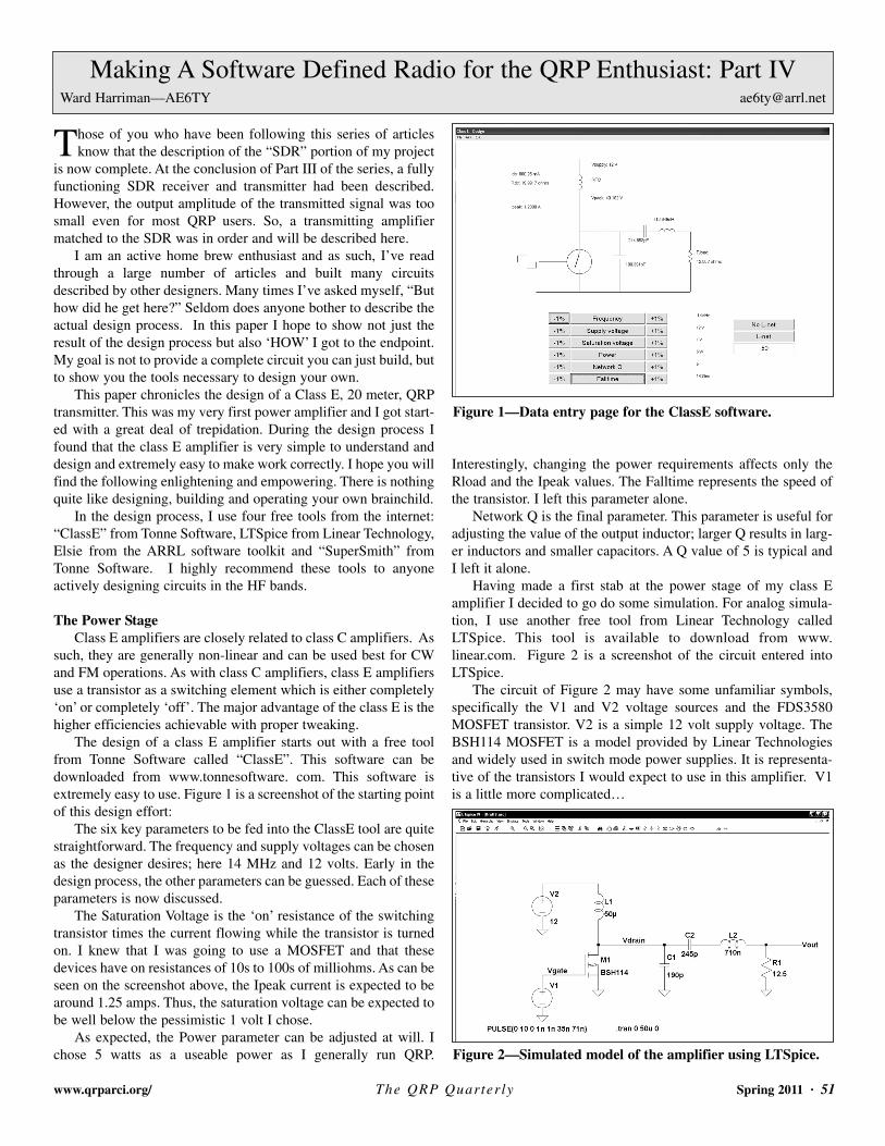
The design of a class E amplifier starts out with a free toolfrom Tonne Software called “ClassE”. This software can bedownloaded from www.tonnesoftware. com. This software isextremely easy to use. Figure 1 is a screenshot of the starting pointof this design effort:
The six key parameters to be fed into the ClassE tool are quitestraightforward. The frequency and supply voltages can be chosenas the designer desires; here 14 MHz and 12 volts. Early in thedesign process, the other parameters can be guessed. Each of theseparameters is now discussed.
The Saturation Voltage is the ‘on’ resistance of the switchingtransistor times the current flowing while the transistor is turnedon. I knew that I was going to use a MOSFET and that thesedevices have on resistances of 10s to 100s of milliohms. As can beseen on the screenshot above, the Ipeak current is expected to bearound 1.25 amps. Thus, the saturation voltage can be expected tobe well below the pessimistic 1 volt I chose.
As expected, the Power parameter can be adjusted at will. Ichose 5 watts as a useable power as I generally run QRP.
Interestingly, changing the power requirements affects only theRload and the Ipeak values. The Falltime represents the speed ofthe transistor. I left this parameter alone.
Network Q is the final parameter. This parameter is useful foradjusting the value of the output inductor; larger Q results in larg-er inductors and smaller capacitors. A Q value of 5 is typical andI left it alone.
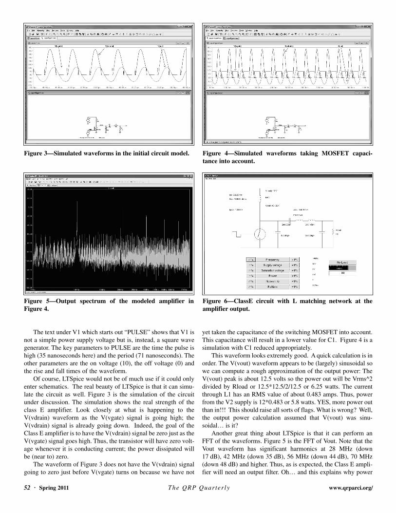
Having made a first stab at the power stage of my class Eamplifier I decided to go do some simulation. For analog simula-tion, I use another free tool from Linear Technology calledLTSpice. This tool is available to download from www.linear.com. Figure 2 is a screenshot of the circuit entered intoLTSpice.
The circuit of Figure 2 may have some unfamiliar symbols,specifically the V1 and V2 voltage sources and the FDS3580MOSFET transistor. V2 is a simple 12 volt supply voltage. TheBSH114 MOSFET is a model provided by Linear Technologiesand widely used in switch mode power supplies. It is representa-tive of the transistors I would expect to use in this amplifier. V1is a little more complicated…
Figure 1—Data entry page for the ClassE software.
Figure 2—Simulated model of the amplifier using LTSpice.
52 · Spring 2011 The QRP Quarterly www.qrparci.org/
The text under V1 which starts out “PULSE” shows that V1 isnot a simple power supply voltage but is, instead, a square wavegenerator. The key parameters to PULSE are the time the pulse ishigh (35 nanoseconds here) and the period (71 nanoseconds). Theother parameters are the on voltage (10), the off voltage (0) andthe rise and fall times of the waveform.
Of course, LTSpice would not be of much use if it could onlyenter schematics. The real beauty of LTSpice is that it can simu-late the circuit as well. Figure 3 is the simulation of the circuitunder discussion. The simulation shows the real strength of theclass E amplifier. Look closely at what is happening to theV(vdrain) waveform as the V(vgate) signal is going high; theV(vdrain) signal is already going down. Indeed, the goal of theClass E amplifier is to have the V(vdrain) signal be zero just as theV(vgate) signal goes high. Thus, the transistor will have zero volt-age whenever it is conducting current; the power dissipated willbe (near to) zero.
The waveform of Figure 3 does not have the V(vdrain) signalgoing to zero just before V(vgate) turns on because we have not
yet taken the capacitance of the switching MOSFET into account.This capacitance will result in a lower value for C1. Figure 4 is asimulation with C1 reduced appropriately.
This waveform looks extremely good. A quick calculation is inorder. The V(vout) waveform appears to be (largely) sinusoidal sowe can compute a rough approximation of the output power: TheV(vout) peak is about 12.5 volts so the power out will be Vrms^2divided by Rload or 12.5*12.5/2/12.5 or 6.25 watts. The currentthrough L1 has an RMS value of about 0.483 amps. Thus, powerfrom the V2 supply is 12*0.483 or 5.8 watts. YES, more power outthan in!!! This should raise all sorts of flags. What is wrong? Well,the output power calculation assumed that V(vout) was sinu-soidal… is it?
Another great thing about LTSpice is that it can perform anFFT of the waveforms. Figure 5 is the FFT of Vout. Note that theVout waveform has significant harmonics at 28 MHz (down17 dB), 42 MHz (down 35 dB), 56 MHz (down 44 dB), 70 MHz(down 48 dB) and higher. Thus, as is expected, the Class E ampli-fier will need an output filter. Oh… and this explains why power
Figure 3—Simulated waveforms in the initial circuit model. Figure 4—Simulated waveforms taking MOSFET capaci-tance into account.
Figure 5—Output spectrum of the modeled amplifier inFigure 4.
Figure 6—ClassE circuit with L matching network at theamplifier output.
www.qrparci.org/ The QRP Quarterly Spring 2011 · 53
out appeared larger than power in.Before proceeding to the output filter, however, there is one
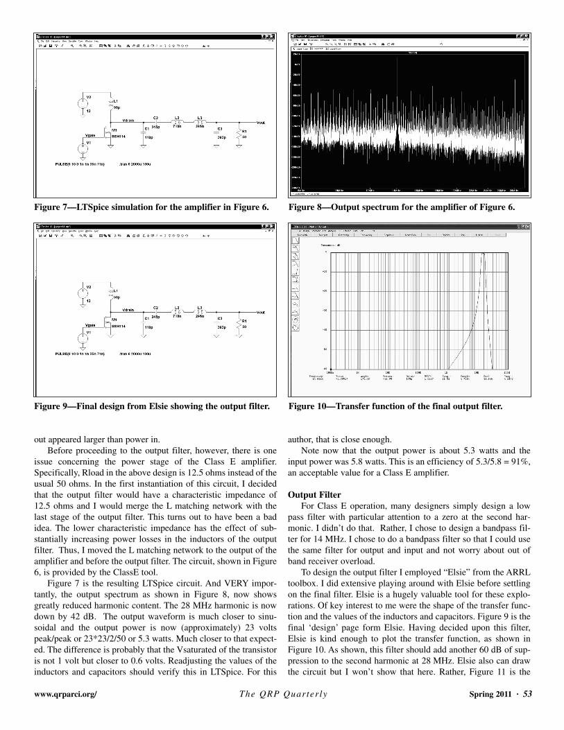
issue concerning the power stage of the Class E amplifier.Specifically, Rload in the above design is 12.5 ohms instead of theusual 50 ohms. In the first instantiation of this circuit, I decidedthat the output filter would have a characteristic impedance of12.5 ohms and I would merge the L matching network with thelast stage of the output filter. This turns out to have been a badidea. The lower characteristic impedance has the effect of sub-stantially increasing power losses in the inductors of the outputfilter. Thus, I moved the L matching network to the output of theamplifier and before the output filter. The circuit, shown in Figure6, is provided by the ClassE tool.
Figure 7 is the resulting LTSpice circuit. And VERY impor-tantly, the output spectrum as shown in Figure 8, now showsgreatly reduced harmonic content. The 28 MHz harmonic is nowdown by 42 dB. The output waveform is much closer to sinu-soidal and the output power is now (approximately) 23 voltspeak/peak or 23*23/2/50 or 5.3 watts. Much closer to that expect-ed. The difference is probably that the Vsaturated of the transistoris not 1 volt but closer to 0.6 volts. Readjusting the values of theinductors and capacitors should verify this in LTSpice. For this
author, that is close enough.Note now that the output power is about 5.3 watts and the
input power was 5.8 watts. This is an efficiency of 5.3/5.8 = 91%,an acceptable value for a Class E amplifier.
Output FilterFor Class E operation, many designers simply design a low
pass filter with particular attention to a zero at the second har-monic. I didn’t do that. Rather, I chose to design a bandpass fil-ter for 14 MHz. I chose to do a bandpass filter so that I could usethe same filter for output and input and not worry about out ofband receiver overload.
To design the output filter I employed “Elsie” from the ARRLtoolbox. I did extensive playing around with Elsie before settlingon the final filter. Elsie is a hugely valuable tool for these explo-rations. Of key interest to me were the shape of the transfer func-tion and the values of the inductors and capacitors. Figure 9 is thefinal ‘design’ page form Elsie. Having decided upon this filter,Elsie is kind enough to plot the transfer function, as shown inFigure 10. As shown, this filter should add another 60 dB of sup-pression to the second harmonic at 28 MHz. Elsie also can drawthe circuit but I won’t show that here. Rather, Figure 11 is the
Figure 7—LTSpice simulation for the amplifier in Figure 6. Figure 8—Output spectrum for the amplifier of Figure 6.
Figure 9—Final design from Elsie showing the output filter. Figure 10—Transfer function of the final output filter.
54 · Spring 2011 The QRP Quarterly www.qrparci.org/
LTSpice circuit. The detail oriented reader will notice the additionof three, 10k resistors. These resistors are needed becauseLTSpice doesn’t work well with undefined voltages on an electri-cal ‘node’. If these resistors were not added then the simulationwould run significantly slower.
Figure 12 is the FFT of the output signal. One of the weak-nesses of LTSpice is that when computing the FFT it does so overa relatively small subset of time. Even when windowed it canreport harmonics which are larger than reality. Still, it can showtrends and relative magnitudes. In the above, the 28 MHz har-monic is shown as 60 dB down from the 14 MHz carrier.
Driving the Power TransistorOne of the real niceties of all switching power amplifiers is the
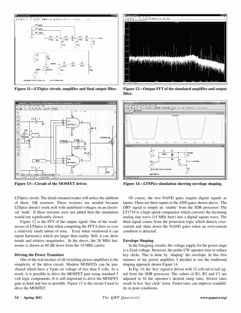
simplicity of the drive circuit. Modern MOSFETs can be pur-chased which have a Vgate on voltage of less than 5 volts. As aresult, it is possible to drive the MOSFET gate using standard 5volt logic components. It is still important to drive the MOSFETgate as hard and fast as possible. Figure 13 is the circuit I used todrive the MOSFET.
Of course, the two NAND gates require digital signals asinputs. There are three inputs to the AND gates shown above. TheDRV signal is simply an ‘enable’ from the SDR processor. TheLT1719 is a high speed comparator which converts the incominganalog sine wave (14 MHz here) into a digital square wave. Thethird signal comes from the protection logic which detects over-current and shuts down the NAND gates when an over-currentcondition is detected.
Envelope ShapingIn the foregoing circuits, the voltage supply for the power stage
is a fixed voltage. However, the polite CW operator tries to reducekey clicks. This is done by ‘shaping’ the envelope. In this firstinstance of my power amplifier, I decided to use the traditionalshaping approach shown Figure 14.
In Fig. 14, the ‘key’ signal is driven with 12 volt rail to rail sig-nal from the SDR processor. The values of R1, R2 and C1 areadjusted to fit the operator’s desired ramp rates. Slower ratesresult in less ‘key click’ noise. Faster rates can improve readabil-ity in poor conditions.
Figure 11—LTSpice circuit; amplifier and final output filter. Figure 12—Output FFT of the simulated amplifier and outputfilter.
Figure 13—Circuit of the MOSFET driver. Figure 14—LTSPice simulation showing envelope shaping.
www.qrparci.org/ The QRP Quarterly Spring 2011 · 55
With the addition of an op amp, one can actually modulate theenvelope and generate an AM signal. With an ‘edge detector’ driv-ing the switch FET, one can actually build a linear amplifier usingclass E as the final stage. There are other ways. The problemsinvolved are brushed over here.
Transmit/Receive SwitchingThere are many ways to provide transmit/receive switching. In
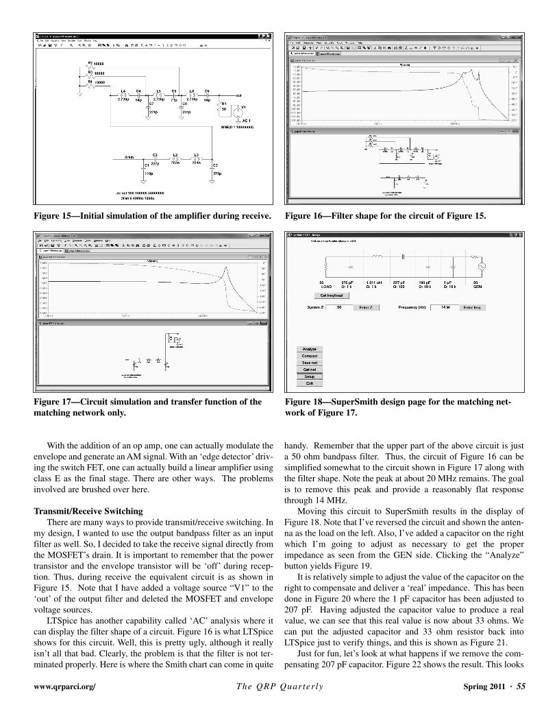
my design, I wanted to use the output bandpass filter as an inputfilter as well. So, I decided to take the receive signal directly fromthe MOSFET’s drain. It is important to remember that the powertransistor and the envelope transistor will be ‘off’ during recep-tion. Thus, during receive the equivalent circuit is as shown inFigure 15. Note that I have added a voltage source “V1” to the‘out’ of the output filter and deleted the MOSFET and envelopevoltage sources.
LTSpice has another capability called ‘AC’ analysis where itcan display the filter shape of a circuit. Figure 16 is what LTSpiceshows for this circuit. Well, this is pretty ugly, although it reallyisn’t all that bad. Clearly, the problem is that the filter is not ter-minated properly. Here is where the Smith chart can come in quite
handy. Remember that the upper part of the above circuit is justa 50 ohm bandpass filter. Thus, the circuit of Figure 16 can besimplified somewhat to the circuit shown in Figure 17 along withthe filter shape. Note the peak at about 20 MHz remains. The goalis to remove this peak and provide a reasonably flat responsethrough 14 MHz.
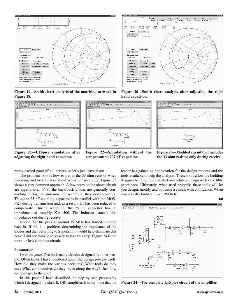
Moving this circuit to SuperSmith results in the display ofFigure 18. Note that I’ve reversed the circuit and shown the anten-na as the load on the left. Also, I’ve added a capacitor on the rightwhich I’m going to adjust as necessary to get the properimpedance as seen from the GEN side. Clicking the “Analyze”button yields Figure 19.
It is relatively simple to adjust the value of the capacitor on theright to compensate and deliver a ‘real’ impedance. This has beendone in Figure 20 where the 1 pF capacitor has been adjusted to207 pF. Having adjusted the capacitor value to produce a realvalue, we can see that this real value is now about 33 ohms. Wecan put the adjusted capacitor and 33 ohm resistor back intoLTSpice just to verify things, and this is shown as Figure 21.
Just for fun, let’s look at what happens if we remove the com-pensating 207 pF capacitor. Figure 22 shows the result. This looks
Figure 15—Initial simulation of the amplifier during receive. Figure 16—Filter shape for the circuit of Figure 15.
Figure 17—Circuit simulation and transfer function of thematching network only.
Figure 18—SuperSmith design page for the matching net-work of Figure 17.
56 · Spring 2011 The QRP Quarterly www.qrparci.org/
pretty darned good (if not better), so let’s just leave it out.The problem now is how to put in the 33 ohm resistor when
receiving and how to take it out when not receiving. Figure 23shows a very common approach. A few notes on the above circuitare appropriate. First, the back/back diodes are generally con-ducting during transmission. On reception, they don’t conduct.Thus, the 25 pF coupling capacitor is in parallel with the MOS-FET during transmission and, as a result, C1 has been reduced tocompensate. During reception, the 25 pF capacitor has animpedance of roughly X = –500. The inductor cancels thisimpedance out during receive.
Notice that the peak at around 19 MHz has started to creepback in. If this is a problem, determining the impedance of thediodes and then returning to SuperSmith would help eliminate thispeak. I did not think it necessary to take this step. Figure 24 is themore-or-less complete circuit.
SummationOver the years I’ve built many circuits designed by other peo-
ple. Often times I have wondered about the design process itself.How did they make the various decisions? What tools do theyuse? What compromises do they make along the way? Just howdid they get to the end?
In this paper, I have described the step by step process bywhich I designed my class E, QRP amplifier. It is my hope that the
reader has gained an appreciation for the design process and thetools available to help the analysis. These tools allow the buddingdesigner to ‘jump in’ and start and refine a design with very littleexperience. Ultimately, when used properly, these tools will letyou design, modify and optimize a circuit with confidence. Whenyou actually build it, it will WORK!
●●
Figure 24—The complete LTSpice circuit of the amplifier.
Figure 19—Smith chart analysis of the matching network inFigure 18.
Figure 21—LTSpice simulation afteradjusting the right hand capacitor.
Figure 22—Simulation without thecompensating 207 pF capacitor.
Figure 23—Modifed circuit that includesthe 33 ohm resistor only during receive.
Figure 20—Smith chart analysis after adjusting the righthand capacitor.