Macintosh® Macintosh IIci€¦ · ð ® Macintosh® Macintosh IIci ð ® Developer Notes Developer...
89
® Macintosh® Macintosh IIci ® Developer Notes Developer Technical Publications © Apple Computer, Inc. 1989
Transcript of Macintosh® Macintosh IIci€¦ · ð ® Macintosh® Macintosh IIci ð ® Developer Notes Developer...

ð ®
Macintosh® Macintosh IIci
ð ®
Developer NotesDeveloper Technical Publications© Apple Computer, Inc. 1989

ð APPLE COMPUTER, INC.
This manual is copyrighted byApple or by Apple’s suppliers,with all rights reserved. Underthe copyright laws, thismanual may not be copied, inwhole or in part, without thewritten consent of AppleComputer, Inc. This exceptiondoes not allow copies to bemade for others, whether ornot sold, but all of the materialpurchased may be sold, given,or lent to another person.Under the law, copyingincludes translating intoanother language.
The Apple logo is a registeredtrademark of AppleComputer, Inc. Use of the“keyboard” Apple logo(Option-Shift-K) forcommercial purposes withoutthe prior written consent ofApple may constitutetrademark infringement andunfair competition in violationof federal and state laws.
© Apple Computer, Inc., 198920525 Mariani AvenueCupertino, CA 95014-6299(408) 996-1010
Apple, the Apple logo,AppleTalk, and Apple IIGS areregistered trademarks ofApple Computer, Inc.
APDA, Apple Desktop Bus,GS/OS, and UniDisk aretrademarks of AppleComputer, Inc.
ITC Zapf Dingbats is aregistered trademark ofInternational TypefaceCorporation.
POSTSCRIPT is a registeredtrademark, and Illustrator is atrademark, of Adobe SystemsIncorporated.
LIMITED WARRANTY ONMEDIA ANDREPLACEMENT
If you discover physicaldefects in the manual or inthe media on which asoftware product isdistributed, APDA willreplace the media or manualat no charge to you providedyou return the item to bereplaced with proof ofpurchase to APDA.
ALL IMPLIEDWARRANTIES ON THISMANUAL, INCLUDINGIMPLIED WARRANTIESOF MERCHANTABILITYAND FITNESS FOR APARTICULAR PURPOSE,ARE LIMITED INDURATION TO NINETY(90) DAYS FROM THEDATE OF THE ORIGINALRETAIL PURCHASE OFTHIS PRODUCT.
Even though Apple hasreviewed this manual,APPLE MAKES NOWARRANTY ORREPRESENTATION,EITHER EXPRESS ORIMPLIED, WITH RESPECTTO THIS MANUAL, ITSQUALITY, ACCURACY,MERCHANTABILITY, ORFITNESS FOR APARTICULAR PURPOSE.AS A RESULT, THISMANUAL IS SOLD “ASIS,” AND YOU, THEPURCHASER, AREASSUMING THE ENTIRERISK AS TO ITS QUALITYAND ACCURACY.
IN NO EVENT WILLAPPLE BE LIABLE FORDIRECT, INDIRECT,SPECIAL, INCIDENTAL,OR CONSEQUENTIALDAMAGES RESULTINGFROM ANY DEFECT ORINACCURACY IN THISMANUAL, even if advisedof the possibility of suchdamages.
THE WARRANTY ANDREMEDIES SET FORTHABOVE ARE EXCLUSIVEAND IN LIEU OF ALLOTHERS, ORAL ORWRITTEN, EXPRESS ORIMPLIED. No Apple dealer,agent, or employee isauthorized to make anymodification, extension, oraddition to this warranty.
Some states do not allow theexclusion or limitation ofimplied warranties orliability for incidental orconsequential damages, sothe above limitation orexclusion may not apply toyou. This warranty gives youspecific legal rights, and youmay also have other rightswhich vary from state tostate.

Contents iii
Contents
Figures and tables / v
1 Introduction / 1Features / 3Compatibility / 7
Disks / 7Memory / 7
History of the Macintosh II Family / 7References / 8
2 Address Mapping / 11Address Space / 13
Programmable Memory Management / 15The memory map / 15
3 The RAM Interface / 17RAM Configuration / 19
Use of RAM by the Video / 21DRAM Requirements and Refresh / 22
Parity and the PGC / 25
4 The Cache Connector / 27Designing For the Cache Connector / 29
Use of a Cache / 29Accessing the Card / 30Electrical Design Guidelines / 31
Power Consumption Guidelines / 37

iv Developer Notes
Mechanical Specifications / 37EMI, Heat Dissipation, and Product Safety / 40
5 The Video Interface / 41On-board Video / 43Video Cables / 49
6 The NuBus Interface / 53NuBus Interface / 55
A RAM and ROM Timing Diagrams 57
B Diagnostic Pinouts 63
C Cache card timing diagrams 71

Figures and tables v
Figures and tables
1 Introduction / 1
Figure 1-1 System block diagram / 5Figure 1-2 Hardware block diagram / 6Table 1-1 System comparisons / 8
2 Address Mapping / 11
Figure 2-1 The physical memory maps / 14Table 2-1 24-bit–to–32-bit mapping mode / 15Figure 2-2 24- and 32-bit address spaces / 16
3 The RAM Interface / 17
Figure 3-1 RAM configurations / 20Figure 3-2 RAM and video block diagram / 22Table 3-1 DRAM access time requirements / 23Figure 3-3 RAM SIMM diagram / 23Table 3-2 Eight-bit DRAM SIMM pinout / 24Table 3-3 Nine-bit DRAM SIMM pinout (for
implementing parity) / 25
4 The Cache Connector / 27
Table 4-1 Cache address space / 30Table 4-2 Cache control trap / 30Table 4-3 Cache connector signals / 32Table 4-4 Cache connector pinout / 34Figure 4-1 Cache connector pin / 36Table 4-5 Cache connector power consumption
limits / 37Figure 4-2 Cache card dimensions, component-side
view / 38Figure 4-3 Cache card dimensions, end view (from front
of computer) / 39

vi Developer Notes
5 The Video Interface / 41
Table 5-1 MON.ID values / 43Figure 5-1 Video timing (not to scale) / 44Table 5-2 RBV signal descriptions / 45Figure 5-2 Video signal sync timing / 46Figure 5-3 Video signal timing for the Apple 13-inch and
12-inch monitors / 47Figure 5-4 Horizontal and vertical video signal timing for
the Apple 15-inch Portrait Monitor / 48Figure 5-5 DB-15 Macintosh IIci Video Connector / 49Figure 5-6 DB-15 Monitor Video Connector / 49Figure 5-7 D-25 Monitor Video Connector / 49Table 5-3 Video connector and cable pinouts / 50Table 5-4 Apple 15-inch Apple Portrait Monitor cable
connections / 50
6 The NuBus Interface / 53
Table 6-1 NuBus slot numbers / 55
A RAM and ROM Timing Diagrams / 57
Figure A-1 RAM burst read timing / 59Figure A-2 RAM random read timing / 60Figure A-3 RAM random write timing / 60Figure A-4 RAM refresh timing / 61Figure A-5 ROM read timing / 62
B Diagnostic Pinouts / 63
Table B-1 Cache connector signal descriptions / 65Figure B-1 Cache connector pinout diagram / 68Table B-2 Cache connector pin diagram / 70
C Cache card timing diagrams / 71
Figure C-1 Timing diagram showing the interactionbetween cache card signals and the optionalParity Generator Chip / 73
Figure C-2 Timing diagram showing the interactionbetween a generic cache card’s signals and theMacintosh IIci’s NuBus connector signals / 74

Figures and tables vii
Figure C-3 Timing diagram showing the interactionbetween a generic cache card and the MacintoshIIci / 75
Figure C-4 Timing diagram showing the interactionbetween a generic cache card’s signals and theMacintosh IIci Nubus’ signals / 76


1
Chapter 1 Introduction
The Apple Macintosh IIci is a new offering in theMacintosh family of computers. It brings with it a historyof compatibility, as well as new features. These old andnew features are described in this chapter.

2 Developer Notes

CHAPTER 1 Introduction 3
Features
The Macintosh IIci is the first in a new series of Macintosh computerscompatible with the Macintosh II family (Macintosh II, Macintosh IIx,and Macintosh IIcx), and offering improved performance and flexibility.The new architecture is based upon the Memory Decode Unit (MDU)and RAM-based video chips (RBV). Key new features are a 25 MHzclock speed and on-board video; most other features are the same as theMacintosh IIcx.
The major new features of the design are:
• MDU/RBV Architecture A new chip set provides memorydecoding and low-cost video by utilizingexisting on-board DRAM for the framebuffer.
• 25 MHz clock speed Faster clock speed for improvedperformance.
• On board video On-board video support for 12” B&W, 13”RGB, and 15” B&W Portrait monitors.
• Burst reads Burst reads from RAM.
• DRAM Parity Optional DRAM parity generation anddetection, when 9-bit DRAM SIMMs and aParity-Generator Chip (PGC) are installed.
• Cache Connector An optional memory cache card.
Additional features that separate the Macintosh IIci from the MacintoshII/IIx/IIcx are:
• RAM Expansion Address space for up to 128 MB of RAM onthe motherboard. 4 Mbit DRAM is nowsupported (and 16 Mbit if it remainscompatible with the 4 Mbit DRAM). Over800 MB of expansion RAM is possible inNuBus slots.
• ROM Expansion A ROM SIMM allows future ROM revisionin the field.

4 Developer Notes
• Slot Expansion Three NuBus expansion slots which allowfull size cards (13” x 4”). Slots support full32 bit address and data.
• Hard Drive support Room for one internal 3 1/2” hard drive withSCSI interface. Additional storage capacitythrough up to 6 additional external drivesconnected to SCSI port on back of CPU.
• Floppy Drive support One internal 1.4 MB Sony 3.5” floppy drive.Support for one external 800K or 1.4 MBSony 3.5” floppy drive. (see Compatibility)
• 68030 Processor True 32-bit processor running at 25 MHz forhigh performance. The 68030 has internal256-byte data and instruction caches as wellas on-chip memory management. Burstreads to the on-chip cache are supported.The 68030 is compatible with existingMacintosh timings and software.
• Memory Management True 32-bit address translation withhardware page replacement.
• Built-in Serial Ports Two Macintosh 8-pin serial ports supportingRS–232, RS–422 and AppleTalk.
• ADB (Apple Desktop Bus) Apple Desktop Bus allows additionalinput devices (e.g. graphics tablet) to beadded at any time. Keyboard and mouse arestandard input devices.
• Numerics Processor The 25 MHz 68882 Floating-PointCoprocessor Unit (FPU) allows high-speed,high-accuracy floating-point computation toIEEE standards.
• Soft Power Control Keyboard power-on and software power-offhelp ensure data integrity on disks. Slotaccess to power control allows power to becontrolled by NuBus cards. The mechanicalon/off button can be locked in the onposition so the computer will automaticallyturn back on after an A/C power outage.
• Real Time Clock Macintosh-compatible clock and parameterRAM with 7-year battery protection.

CHAPTER 1 Introduction 5
• Sound Apple sound chip provides Macintosh-compatible sound and four-voice synthesisin hardware.
• Video On-board video support for the Apple 12-inch B&W, 13-inch RGB, and 15-inch B&WPortrait monitors. NuBus video-card optionsare also available.

6 Developer Notes
• Figure 1-1 System block diagram
FPU
REV
RAM Array
PGC
ROM
RTC
VIA
SCC
SCSI
SWIM
Sound
NuBus
Video DAC Video Post
Desktop Bus
Two Serial Ports
External SCSI Port
External Floppy Drive Port
Stereo Output
Internal SCSI Port (Hard Disk)
Internal Floppy Drive Port
Internal Speaker
Three NuBus Ports
Cache Connector
CPU
MDU
CHAPTER 1 Introduction 7
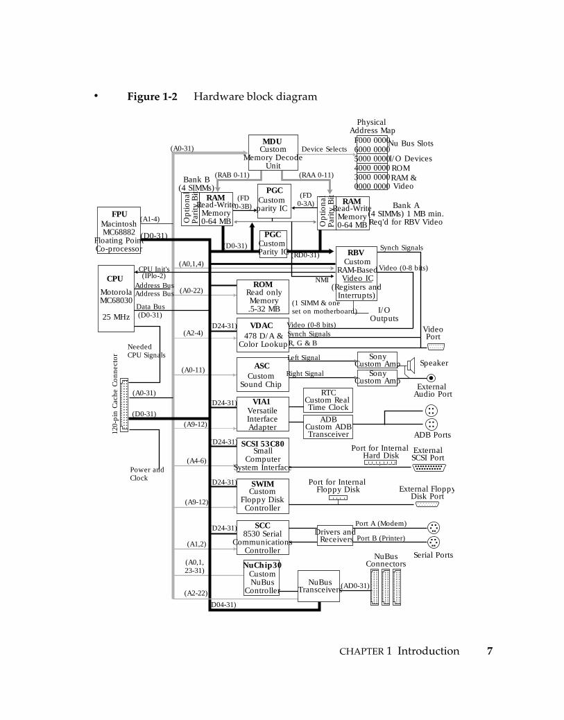
• Figure 1-2 Hardware block diagram
CustomMemory Decode
Unit
PGCCustomparity IC
Optio
nal
Par
ity B
itRead-WriteMemory0-64 MB O
ptio
nal
Par
ity B
it
Read-WriteMemory0-64 MB
RAM
Bank B(4 SIMMs)
Bank A(4 SIMMs) 1 MB min.Req'd for RBV Video
Nu Bus Slots
I/O DevicesROMRAM &Video
Device Selects
(FD0-3B)
F000 00006000 00005000 00004000 00003000 00000000 0000
(FD0-3A)
I/OOutputs
CustomRAM-BasedVideo IC
(Registers andInterrupts)
Custom Parity IC
PGC
(A0-31)
(RAA 0-11)(RAB 0-11)
Physical Address Map
SonyCustom Amp
FPUMacintoshMC68882
Floating PointCo-processor
CPU
MotorolaMC68030
25 MHz
(A1-4)
(D0-31)
CPU Init's(IPlo-2)
Address BusAddress Bus
(D0-31)Data Bus
(A0-22)
(A0,1,4)
(A2-4)
RTCCustom Real Time Clock
SonyCustom Amp
ADBCustom ADBTransceiver
Drivers and Receivers
ExternalSCSI Port
External FloppyDisk Port
NuBusTransceivers
Port for Internal Hard Disk
Port for Internal Floppy Disk
Read onlyMemory.5-32 MB
VIA1
SWIMCustom
Floppy DiskController
SCC8530 Serial
CommunicationsController
SmallComputer
System Interface
Synch Signals
Video (0-8 bits)
CustomSound Chip
ASC
NeededCPU Signals
(A0-31)
(D0-31)
Power andClock
(A0-11)
(D24-31)
(A9-12)
(D24-31)
(A4-6)
(D24-31)
(A9-12)
(D24-31)
(A1,2)
(A0,1,23-31)
(AD0-31)
(1 SIMM & one set on motherboard)
VersatileInterfaceAdapter
SCSI 53C80
ROM
VDAC478 D/A &
Color Lookup
NuChip30CustomNuBus
Controller
VideoPort
NuBusConnectors
120-
pin
Cac
he
Connec
tor
(D24-31) Video (0-8 bits)Synch SignalsR, G & B
Left Signal
Right Signal
Port A (Modem)
Port B (Printer)
(D04-31)
(A2-22)
RBV
MDU
RAM
Serial Ports
External Audio Port
ADB Ports
Speaker
(D0-31)(RD0-31)
NMI

8 Developer Notes
Compatibility
Disks
The external floppy drive port on this product does not support the400K floppy drive. It does support 400K disks used in the 800K drive.
Memory
Physical memory is not contiguous, as it is on the Macintosh II, IIx, andIIcx. The 68030 on-chip MMU is used to join the discontiguous blocks ofphysical memory to present contiguous logical memory to applicationsoftware. RAM must be 80 ns access time (or faster), fast page mode.For additional RAM specifications, see see Chapter 3, “The RAMInterface.”
History of the Macintosh II Family
The Macintosh IIci continues the modular design center. Macintosh IIcxbegan this evolution by taking the Macintosh IIx and removing threeNuBus slots and a floppy-disk drive. Most other changes from theMacintosh IIx were in appearance, and Apple’s official approval (andencouragement, even) to stand it up on end. The box was redesigned,the power supply and power-on circuitry redesigned, and the hard-diskdrive was changed from 5 1/2” to 3 1/2”.
The Macintosh IIci project continues this evolution with a completelynew architecture, built around the Memory Decode Unit (MDU) andRAM Based Video (RBV) chips. The NuChip was also modified,becoming the NuChip30, to work efficiently with the 68030 bus.

CHAPTER 1 Introduction 9
• Table 1-1 System comparisons
Macintosh II Macintosh IIx Macintosh IIcx Macintosh IIci
ð Macintosh II ð Macintosh IIx ð Macintosh IIcx ð Macintosh IIci
processor 16 MHz 68020 16 MHz 68030 16 MHz 68030 25 MHz 68030
coprocessor 16 MHz 68881 16 MHz 68882 16 MHz 68882 25 MHz 68882
NuBus 6 NuBus Slots 6 NuBus Slots 3 NuBus Slots 3 NuBus Slots
Other none none none Cache Connector
architecture GluChip/NuChip GluChip/NuChip GluChip/NuChip MDU/RBV/NuChip30
Parity none none none optional PGC
int. floppy 2 internal floppies 2 internal floppies 1 internal floppy 1 internal floppy
ext. floppy no external floppy no external floppy 1 external floppy 1 external floppy
hard drive internal 5 1/4” or 3 1/2”
hard drive
internal 5 1/4” or 3 1/2”
hard drive
internal 3 1/2” hard drive internal 3 1/2” hard
drive
ROM socket DIP SIMM DIP & SIMM DIP & SIMM
ROM speed 150 ns 150 ns 150 ns 150 ns
RAM speed 120 ns 120 ns 120 ns 80 ns fast page mode
References
Additional information relating to this design can be found in thefollowing documents.
• MC68030 Enhanced 32-Bit Microprocessor User’s Manual, SecondEdition, Motorola, MC68030UM/AD REV 1, 1989.
• MC68882 Floating-Point Coprocessor User’s Manual, Motorola,Prentice-Hall, 1985.
• NuBus Specification (Draft 1.1), NuBus Subcommittee, 1985.
• Product Databook, Brooktree, First Edition, 1988
• SCSI Small Computer System Interface, ANSI X3T9.2/82-2 Rev. 17B.

10 Developer Notes
• Controller Products Data Book (VIA), Rockwell, 1987.
• Z8030 Z-BUS SCC/Z8530 SCC Serial Communications Controller,Product Specification, Zilog, September 1986.

11
Chapter 2 Address Mapping
The Macintosh IIci uses a memory mapping scheme whichis implemented by a new custom IC, the Memory DecodeUnit. The memory map as controlled by the MDU, isdescribed in this chapter.

12 Developer Notes

CHAPTER 2 Address Mapping 13
Address Space
The address space is decoded by the Memory Decode Unit (MDU). Onpower up, ROM is mapped by the MDU to physical location $0000 0000.This enables the starting address, retrieved by the 68030 on reset, to bestored in ROM. After the first access to the true ROM address space($4000 0000 through $4FFF FFFF), the normal memory map is imposedby the MDU. The only change from one map to the other is that in thepower-up map ROM is selected for addresses $0000 0000-3FFF FFFF,whereas the normal map selects RAM for that address space as shownin Figure 2-1.

14 Developer Notes
• Figure 2-1 The physical memory maps
NuBus SuperSlot Space
Reserved (No device assigned)
NuBus Slot Space
(Slots 4 - 6)
Expansion I/O Space
Reserved ROM Space
I/O Devices
ROM
(32m Bytes)
(8M Bytes)
(2M Bytes)
(1M Bytes)
More Images of ROM
(32M Bytes)
NuBus SuperSlot Space
Reserved (No device assigned)
NuBus Slot Space
(Slots 4 - 6)
Expansion I/O Space
Reserved ROM Space
I/O Devices
(512k Bytes)
Map on Power-up(before first access to
$4000 0000-$4FFF FFFF)
Normal Map(after first access to
$4000 0000-$4FFF FFFF)
$ F100 0000
$ F000 0000
$ C000 0000
$ 9000 0000
$ 6000 0000
$ 10000 0000
$ 4200 0000
$ 4800 0000
$ 4020 0000
$ 4010 0000
$ 4008 0000
$ 4000 0000
$ 0800 0000
$ 0500 0000
$ 0200 0000
$ 0100 0000
$ 0040 0000
$ 0010 0000
$ 0008 0000
$ 0000 0000
$ 5300 0000
$ 5000 0000
$ 0440 0000
$ 0410 0000
$ 0400 0000
(16M Bytes)
(4M Bytes)
(1M Bytes)
ROM
(32m Bytes)
(8M Bytes)
(2M Bytes)
(1M Bytes)
(16M Bytes)
(4M Bytes)
(512k Bytes)
(64M Bytes)
(16M Bytes)
(4M Bytes)
RAMBank B
(1M Bytes)
(64M Bytes)
RAMBank A
Reserved RAM Space
Video Screen Buffer
(1M Bytes)
(SIMMs 1-4)
Duplicate Imageof ROM
(512M Bytes)

CHAPTER 2 Address Mapping 15
Programmable Memory Management
Memory mapping is performed by the Memory Management Unit(MMU), whose function is built into the MC68030 processor. Havingthe MMU function built into the microprocessor saves one wait stateover the use of an external MC68851 PMMU or Apple HMMU with theMC68020 on the Macintosh II. However, the 68030 on-chip MMUprovides only a subset of the 68851’s capabilities. The 68030 allowsmemory management that is required when running virtual memorysystems such as A/UX.
Software determines the memory size at power-on and compiles a tabledescribing the current memory configuration. The MMU is thenprogrammed based on this table to provide contiguous logical memoryfrom the potentially non-contiguous physical segments in Banks A andB.
The memory map
The 24/32 bit Memory Map is designed to allow existing Macintoshsoftware to use a 24 bit address mode while new software can use thefull 32 bit address space. It is implemented as a simple direct mapping,as shown in Table 2-1 and Figure 2-2. The memory maps are set up bythe 68030’s on-chip MMU. Note that this memory mapping schememaps the video frame buffer into the NuBus superslot space.

16 Developer Notes
• Table 2-1 24-bit–to–32-bit mapping mode
Usage 24 bit Address Range 32 bit Address Rangefrom to from to
RAM $xx00 0000 $xx7F FFFF $0000 0000 $07FF FFFF
ROM $xx80 0000 $xx8F FFFF $4000 0000 $400F FFFF
(not on IIci) NuBus Address $9 $xx90 0000 $xx9F FFFF $F900 0000 $F90F FFFF
(not on IIci) NuBus Address $A $xxA0 0000 $xxAF FFFF $FA00 0000 $FA0F FFFF
(not on IIci) NuBus Address $B $xxB0 0000 $xxBF FFFF $FB00 0000 $FB0F FFFF
Slot 4 NuBus Address $C $xxC0 0000 $xxCF FFFF $FC00 0000 $FC0F FFFF
Slot 5 NuBus Address $D $xxD0 0000 $xxDF FFFF $FD00 0000 $FD0F FFFF
Slot 6 NuBus Address $E $xxE0 0000 $xxEF FFFF $FE00 0000 $FE0F FFFF
I/O Space $xxF0 0000 $xxFF FFFF $5000 0000 $500F FFFF

CHAPTER 2 Address Mapping 17
• Figure 2-2 24- and 32-bit address spaces
I\OF0 0000
NuBus
90 0000
ROM
8F FFFF
80 0000
7F FFFF
RAM
00 0000
F0FF FFFF
NuBus Slots
F100 0000
Reserved
F000 0000
NuBus Super-Slots
6000 00005FFF FFFF
I\O5000 0000
3FFF FFFF
4FFF FFFF
RAM
4000 0000
0000 0000
24 bit LogicalAddress Space
32 bit LogicalAddress Space
32 Bit PhysicalAddress Space
FFFF FFFFFFFF FFFFNuBusSlots
F100 0000
F0FF FFFF
Reserved
F000 0000
NuBus Super-Slots
6000 0000
5FFF FFFF
I/O5FFF FFFF
4FFF FFFFROM
4000 000007FF FFFF
RAM Bank B
0800 0000
FF FFFF
FF FFFF
FFFF FFFF
ROM
ExpansionRAM
07FF FFFF
0400 000003FF FFFF
RAM Bank A
0000 0000
FFFF FFFF


19
Chapter 3 The RAM Interface
The Macintosh IIci introduces new memory read andwrite techniques—such as burst reads and paritychecking—which are implemented in RAM SIMMS. Thischapter details the electrical and physical details of theRAM, as well as the optional Parity Generator Chip forproviding memory parity checking. How video makesuse of RAM, and RAM refresh are also described in thischapter.

20 Developer Notes

CHAPTER 3 The RAM Interface 21
RAM Configuration
The Random Access Memory (RAM) interface on the motherboard isdesigned to support from 1 MB to 128 MB of RAM. The interfacesupports burst-read mode which allows a 5 clock initial access followedimmediately by three 2 clock accesses. The RAM is mounted in SingleInline Memory Modules (SIMMs) which each contain up to eight ornine Dynamic Random Access Memories (DRAMs) on a PC board.Nine-bit DRAM SIMMs are necessary only if the optional ParityGenerator Checker (PGC) is installed and parity checking is desired, butparity checking will be enabled only if all installed SIMMs are 9-bitSIMMs. RAM is divided into two banks, A and B, of four SIMM socketseach. Each bank may contain either no RAM or four 256K SIMMs(made from 1 Mbit fast-page-mode parts), four 1 MB SIMMs, four 4 MBSIMMs, or four 16 MB SIMMs. The amount of motherboard RAM ischanged by installing four of the same size SIMMs into either bank.(See Figure 3-1). Bank A must have DRAM installed in order to use on-board video.
Note that although the Macintosh IIci supports parity checking, thestandard machine configuration will be shipped with eight-bit DRAMSIMMs. For parity, special units with the PGC and nine-bit DRAMSIMMs must be ordered.
Each bank of RAM is decoded into one of two fixed contiguous 64 MBaddress spaces. Since these banks are at fixed physical locations (seePhysical Memory Map), the overall RAM address space will not becontiguous unless Bank A is full (16 Mbit DRAM parts). Bank Aoccupies physical address $0000 0000 to $03FF FFFF and Bank Boccupies physical addresses $0400 0000 to $07FF FFFF. Unless 16 MbitDRAMs are used in a bank of memory, some part of the 64 MB addressspace will be unused. Such space will wrap, containing multiple imagesof the existing RAM in that bank’s address space. For example, if 1 MBof RAM is inserted into Bank A then $0000 0000 to $000F FFFF willcontain the normal image and $0001 0000 to $0001 FFFF will contain thesecond image, and so on, with a total of 63 copies of the normal 1 MBaddress range. This address wrapping allows the ROM to determinehow much memory is present in each bank.

22 Developer Notes
• Figure 3-1 RAM configurations
8 M
egab
yte
Syste
m
1 M
egab
yte
Syste
m2
Meg
abyt
e Sys
tem
4 M
egab
yte
Syste
m
5 M
egab
yte
Syste
m
16 M
egab
yte
Syste
m17
Meg
abyt
e Sys
tem
20 M
egab
yte
Syste
m32
Meg
abyt
e Sys
tem
Em
pty
Ban
k
Em
pty
Ban
k
Em
pty
Ban
k
Fou
r 1
MB
SIM
Ms
Fou
r 1
MB
SIM
Ms
Fou
r 1
MB
SIM
Ms
Fou
r 1
MB
SIM
Ms
Fou
r 1
MB
SIM
Ms
Fou
r 4
MB
SIM
Ms
Fou
r 4
MB
SIM
Ms
Fou
r 4
MB
SIM
Ms
Fou
r 4
MB
SIM
Ms
Fou
r 4
MB
SIM
Ms
Fou
r 25
6 K
B S
IMM
s
Fou
r 25
6 K
B S
IMM
s
Fou
r 25
6 K
B S
IMM
s
Fou
r 25
6 K
B S
IMM
s
Fou
r 25
6 K
B S
IMM
s
NOTES:
1 Banks A and B are interchangeable. For best performance with on-board video, putthe smaller SIMMs in bank A.
2 Use of on-board video requires DRAM in bank A.
3 256K SIMMs will be made from 256K x 4 fast page mode DRAM parts (1 MBittechnology), unless 256K x 1 fast page mode DRAM parts (256 KBit technology)become more readily available.

CHAPTER 3 The RAM Interface 23
Use of RAM by the Video
If the on-board video is used, RAM must be installed in Bank A becausethe frame buffer is maintained beginning at physical address $00000000. The RBV’s frame buffer is variable in size, depending on thecurrently selected bit-depth and on the size of the video monitorplugged in to the on-board video port. The RBV will require only theamount of memory to hold the contents of the screen; no additionalmemory is used for the frame buffer by the RBV. Software willdetermine the maximum (default, or previous selection by the user)video bit depth to be made available at startup, and set aside thatmemory for video. If a smaller bit depth than this maximum is selectedby the user, operating system software may make use of this additionalspace.
The RBV requests memory in bursts and the MDU passes the data frommemory, automatically incrementing a pointer to the current location inthe frame buffer. The RBV tells the MDU to reset this pointer at the endof a screen, and the MDU sets the frame buffer pointer back to physicaladdress $0000 0000. (All addresses dealt with by the MDU must bephysical because all logical memory mapping is performed by the68030’s on-board MMU.)
The operating system may map this region of memory elsewhere, inorder to make it look like any other video device. The operating systemdecides at startup how much of Bank A to devote to video, and howmuch may be mapped to the normal RAM address space.
Video accesses affect only Bank A memory access because the data busbetween the RAM banks can be disconnected by an F245 buffer asshown in Figure 3-2. This allows the RBV to fetch data from Bank Awithout interrupting CPU access to Bank B or I/O devices. Each bankof RAM is accessed independently by the MDU, so it can decodeaddresses for the CPU and the RBV at the same time withoutinterference.
For clarity, only the necessary components are illustrated in Figure 3-2.

24 Developer Notes
• Figure 3-2 RAM and video block diagram
CPU
Data BusMotorolaMC68030
(D0-31
Address Bus
(A0-31
(D0-31)
(A0-31
(RD0-31)
RAMBank A
RAM Addresses
F245Bus
Buffers
RAMBank B
MDU
RBV
DRAM Requirements and Refresh
The RAM interface requires 80 ns RAS access time DRAMs with CASbefore RAS refresh and fast page mode. The Table 3-1 gives moredetailed DRAM specifications. These DRAMs must be mounted on 30pin SIMMs with bypass capacitors. Table 3-2 and Table 3-3 show thepinout for the SIMMs both with and without parity, and the connectionsmade to the processor bus.
• Table 3-1 DRAM access time requirements
RAS Access Time 80 ns
CAS Access Time 20 ns
Access Type Fast Page Mode
Refresh Type CAS~ before RAS~
Refresh Period 15.6 µs

CHAPTER 3 The RAM Interface 25
RAM refresh is performed by the MDU with CAS before RAS cycles.The refresh cycles are six CPU clocks long. Refresh is initiated at thesame time in both banks of RAM every 15.6 µs; however, it continuesindependently in each bank so that if it must be held off until thecompletion of a CPU or video access in one bank, the other bank’srefresh is not also held off. Refresh does not affect the processor at all ifthe processor is accessing anything except RAM.
• Figure 3-3 RAM SIMM diagram
2.900"
0.100"
3.500"
0.080"
R 0.067
0.300"
0.250"
0.133"
R 0.125"
3.234"
0.070"
0.100"
0.050"[+.004/-.00
1 30
0.400"

26 Developer Notes
• Table 3-2 Eight-bit DRAM SIMM pinout
Pin # SIMM Processor Bus Pin # SIMM Processor BusFunction Function Function Function
1 +5V +5V 16 DQ4 D4, D12, D20, orD28
2 CAS~ CASLL~, CASLM~, 17 RA8 A19RAS, A18CASCASUM~ or CASUU~ 18 RA9 A21RAS, A20CAS
3 DQ0 D0, D8, D16, or D24 19 RA10 A23RAS, A22CAS4 RA0 A6RAS, A2CAS 20 DQ5 D5, D13, D21, or
D295 RA1 A7RAS, A3CAS 21 WE~ RAMRW~6 DQ1 D1, D9, D17, or D25 22 +5V +5V7 RA2 A8RAS, A4CAS 23 DQ6 D6, D14, D22, or
D308 RA3 A9RAS, A5CAS 24 RA11 A24RAS, A25CAS9 GND GND 25 DQ7 D7, D15, D23, or
D3110 DQ2 D2, D10, D18, or D26 26 NC NC11 RA4 A11RAS, A10CAS 27 RAS~ RAS0~ or RAS1~12 RA5 A13RAS, A12CAS 28 NC Pullup to +5V13 DQ3 D3, D11, D19, or D27 29 NC NC14 RA6 A15RAS, A14CAS 30 +5V +5V15 RA7 A17RAS, A16CAS

CHAPTER 3 The RAM Interface 27
• Table 3-3 Nine-bit DRAM SIMM pinout (for implementing parity)
Pin # SIMM Processor Bus Pin # SIMM Processor BusFunction Function Function Function
1 +5V +5V 17 RA8 A19RAS, A18CAS2 CAS~ CASLL~, CASLM~, 18 RA9 A21RAS, A20CAS
CASUM~ or CASUU~ 19 RA10 A23RAS, A22CAS3 DQ0 D0, D8, D16, or D24 20 DQ5 D5, D13, D21, or
D294 RA0 A6RAS, A2CAS 21 WE~ RAMRW~5 RA1 A7RAS, A3CAS 22 +5V +5V6 DQ1 D1, D9, D17, or D25 23 DQ6 D6, D14, D22, or
D307 RA2 A8RAS, A4CAS 24 RA11 A24RAS, A25CAS8 RA3 A9RAS, A5CAS 25 DQ7 D7, D15, D23, or
D319 GND GND 26 PDO PDO0, PDO1,
PDO2,10 DQ2 D2, D10, D18, or D26 or PDO311 RA4 A11RAS, A10CAS 27 RAS~ RAS0~, or RAS1~12 RA5 A13RAS, A12CAS 28 PCAS~ CASLL~,
CASLM~,13 DQ3 D3, D11, D19, or D27 CASUM~ or
CASUU~14 RA6 A15RAS, A14CAS 29 PD PD0, PD1, PD2, or15 RA7 A17RAS, A16CAS PD316 DQ4 D4, D12, D20, or D28 30 +5V +5V
Parity and the PGC
Parity is generated by the optional Parity Generator Chip (PGC). If youwant parity checking you must order the Macintosh IIci configured withthe PGC and nine-bit DRAM SIMMs.
On all reads in the RAM address space, the PGC generates an internalparity bit from each byte of the data bus, and compares it to the bit readfrom SIMM’s parity bit. If the two parity bits do not agree, and parity isenabled, the PGC generates a parity error.

28 Developer Notes
Note that parity is always written to the parity bit if the PGC is present.If the bit is not physically present on the SIMM module, it is simplyignored—a problem only exists if parity is read from the bit (i.e., parityis enabled) when the bit is not present (i.e., eight-bit DRAM SIMMs arein use).
Parity checking starts out disabled; the startup code will determine ifthe PGC is installed, and if parity memory is installed, and enable parityif appropriate. If a parity error is detected you will be told “A MemoryParity Error Has Occurred” and must reboot your Macintosh IIci.

29
Chapter 4 The Cache Connector
A cache card is a way of increasing system performance inthe Macintosh IIci. The cache connector providesdevelopers with infinite flexibility in implementingcustom-designed cache hardware. The electrical andphysical specifications of the cache connector and otherimplementation design considerations are provided in thischapter.

30 Developer Notes

CHAPTER 4 The Cache Connector 31
Designing For the Cache Connector
The Macintosh IIci is designed with a special purpose cache connector.The signals provided are optimized for a cache design, not a generalpurpose interface. A 120-pin EuroDIN connector is provided on themotherboard. This is the same connector as the SE/30 provides, butSE/30 cards are not compatible with the Macintosh IIci (see warningbelow). In addition to a new pinout, optimized for cache design, theMacintosh IIci cache connector is incompatible with the SE/30 due to:
• Different form factor: The space inside the Macintosh IIci differsfrom the SE/30.
• No space for an external connector: The Macintosh IIci has no backpanel cutout for I/O connection to a card in the cache connector.
• Different clock speed: The Macintosh IIci runs at 25 MHz, rather than16 MHz like the SE/30.
• Different Power Limit: 5 watts of power is allocated at +5 volts only.
♦ Warning The Macintosh IIci cache connector is not designed forSE/30 cards. The pinouts are different, so cardsdesigned for the SE/30 will not work on Macintosh IIci,and may damage both the computer and the card. ♦
Do not cache accesses made by bus masters other than the 68030, sincethey may not know how to retry. Apple strongly suggests the use ofsynchronous logic (clocked by CPUCLK) on a cache card.
See Appendix A for detailed RAM and ROM waveforms. Forinformation about using the Cache Connector for diagnostics, seeAppendix B.
32 Developer Notes
Use of a Cache
A cache card should operate transparently to user programs. The cachewill be physical, as it has no access to the 68030’s on-board MMU, socache coherency should not be a problem. In addition, for a physicalcache there should be no reason to flush the cache except when enablingthe cache. The cache should also flush on a RESET~, but the systemdoesn’t rely on this. The MMU table will mark the NuBus slot spaceand all I/O space as non-cacheable. Accesses to these locations by the68030 will not be cached.
Accessing the Card
Address space has been reserved for use by the cache card, allowing testsoftware to access both cache data memory and cache tag memory.Cache data should be accessed in the range from $5200 0000 through$527F FFFF (8 MB maximum), and Tag memory should be accessed inthe range from $5280 0000 through $52FF FFFF (8 MB maximum).Cache cards must decode these address ranges themselves; no selectsignal is provided on the connector. Note that the cache card’s addressspace is not accessible through the 24-bit memory map. Test softwarerunning in 24-bit mode must use the SwapMMUMode trap to enter 32-bitmode before it can access cache card memory.
• Table 4-1 Cache address space
From To
Cache Data Memory $5200 0000 $527F FFFFCache Tag Memory $5280 0000 $52FF FFFF
Cache card enable, disable, and flush are controlled by ROM traps.They are called using a selector off the HWPriv (A098) trap.

CHAPTER 4 The Cache Connector 33
• Table 4-2 Cache control trap
Function Selector
EnableExtCache 4
DisableExtCache 5
FlushExtCache 6
The organization of a particular card’s data and tag memory will bedetermined by the card. System software will not make anyassumptions about the cache card’s organization, and only the card’stest software should directly access cache card RAM.
Electrical Design Guidelines
The Macintosh IIci cache connector has a pinout specifically tailored to acache implementation. The only unusual signal on the cache connectoris CACHE. This active high signal disables the memory controller(MDU), so that it will not start a memory cycle and will allow the cacheto supply the data instead. The active high CACHE signal musttransition at the same time as the active low address strobe (AS~), orearlier. Asserting CACHE prevents the memory controller frombeginning a RAM, ROM, or NuBus cycle. If CACHE is asserted afterthe memory controller has started a cycle, that cycle is not affected.CACHE has no effect on memory controller cycles for I/O devices.Since CACHE must be asserted at AS~, a cache controller will mostlikely leave CACHE asserted except when the cache is not active (e.g.,CIOUT~ is asserted, CENABLE~ is negated, or an alternate bus masterowns the bus as indicated by an asserted BGACK~ signal).

34 Developer Notes
Note that NuBus cards can access each other without that transactionappearing on the CPU bus. This can lead to inconsistencies betweenmemory on a NuBus card, for example, and the cached version of thatmemory. For this reason, the operating system always marks theNuBus address space as non-cacheable, as controlled by the MC68030’son-chip memory management unit (MMU).
The BGACK~ signal is not driven high quickly enough by themotherboard. The cache card should pull BGACK~ up to +5 V with a2.2 K-ohm resistor, and double-rank synchronize BGACK~ before usingit. To double-rank synchronize, put BGACK~ through two DQ flip-flops clocked by CPUCLK, and use the output from the second flip-flop.
Table 4-3 gives details of each cache connector signal. The categorylabeled “I/O” indicates Input or Output (or both, in some cases) fromthe cache card’s point of view. “Motherboard Drives” specifies thecurrent that the motherboard is able to supply, and the capacitiveloading that the motherboard can tolerate. “Card Drives” specifies thecurrent that the card must be able to supply, and the maximumcapacitive loading that the motherboard would exhibit. “MasterDrives” is applicable to input signals and “Card Drives” is applicable tooutput signals; thus, signals which are only input or output will havethe appropriate driving specification left blank.
Most of the cache connector signals are designed to drive two 74LSinputs (a standard 74LS input load is 20 µA high, 0.2 mA low). Someexceptions will drive only one 74LS input,. These are: RESET~; thehigh order data byte (D24-D31); and the function codes (FC0-FC2).CPUCLK will drive only a CMOS input (a standard CMOS input load is10 µA high, 10 µA low).
Refer to Appendix C for the timing diagrams of the cache cardconnector signals.
• Table 4-3 Cache connector signals
Signal Signal I/O Motherboard Card Motherboar
d
Name Description Drives Drives Note Pins
A0-A31 Address Bus I 40 µA/0.4 mA
30 pF
1 KΩ Pullup
(A30-A31
only)
32

CHAPTER 4 The Cache Connector 35
D0-D23 Data Bus I/O 40 µA/0.4 mA
30 pF
150 µA/1 mA
100 pF
24
D24-D31 20 µA/0.2 mA
15 pF
300 µA/1 mA
100 pF
8
RESET~ Reset I 20 µA/0.2 mA
15 pF
Open
Collector
470Ω pullup
1
BERR~ Bus Error I/O 40 µA/0.4 mA
30 pF
100 µA/8 mA
50 pF
1 KΩ pullup 1
HALT~ Halt I/O 40 µA/0.4 mA
30 pF
100 µA/8 mA
50 pF
1 KΩ pullup 1
FC0-FC2 Function Codes I 20 µA/0.2 mA
30 pF
1 KΩ pullup 3
BG~ Bus Grant I 40 mA/0.4 mA
30 pF
1
BGACK~ Bus Grant Acknowledge I 40 mA/0.4 mA
30 pF
1
SIZ0-SIZ1 Transfer Size I 40 µA/0.4 mA
30 pF
2
AS~ Address Strobe I 40 µA/0.4 mA
30 pF
1 KΩ pullup 1
R/W~ Read/Write I 40 µA/0.4 mA
30 pF
1 KΩ pullup 1
STERM~ Synchronous Termination I/O 40 µA/0.4 mA
30 pF
100 µA/8 mA
50 pF
1 KΩ pullup 1
CBACK~ Cache Burst Acknowledge I 40 µA/0.4 mA
30 pF
1 KΩ pullup 1
CBREQ~ Cache Burst Request I 40 µA/0.4 mA
30 pF
1 KΩ pullup
CIOUT~ Cache Inhibit Out I 40 µA/0.4 mA
30 pF
1 KΩ pullup 1
DS~ Data Strobe I 40 µA/0.4 mA
30 pF
1 KΩ pullup
RMC~ Read Modify write Cycle I 40 µA/0.4 mA
30 pF
1 KΩ pullup
CPUCLK CPU Clock (25 MHz) I 10µA/10µA
15 pF
1
CACHE Memory Controller Disable
for Cache Access
O 8 mA/1 mA
30 pF
1 KΩpulldown
1
CFLUSH~ Cache Flush I 40 µA/0.4 mA
30 pF
1

36 Developer Notes
CENABLE~ Cache Enable I 40 µA/0.4 mA
30 pF
1
n.c. no connection 15
Vcc +5 volts I 1 A 11
GND Ground (Vss) I 11

CHAPTER 4 The Cache Connector 37
• Table 4-4 Cache connector pinout
A B CA30 1 RESET~ 1 R/W~
HALT~ 2 A29 2 STERM~A31 3 A25 3 A28A26 4 A27 4 Vcc
RMC~ 5 A24 5 CFLUSH~D31 6 GND 6 VccD30 7 D29 7 n.c.D28 8 D27 8 GNDD26 9 D25 9 VccD24 10 D23 10 GNDD22 11 D21 11 GNDD20 12 D19 12 n.c.D18 13 D17 13 CENABLE~D16 14 Vcc 14 VccA22 15 A21 15 VccA20 16 A19 16 GNDA18 17 A17 17 n.c.A16 18 A15 18 GNDA14 19 A13 19 VccA12 20 A11 20 n.c.A10 21 GND 21 GNDFC1 22 A9 22 VccA8 23 n.c. 23 GNDFC2 24 FC0 24 CIOUT~D15 25 D14 25 n.c.D13 26 D12 26 n.c.D11 27 D10 27 CBREQ~D9 28 D8 28 D7D6 29 BGACK~ 29 D5D4 30 D3 30 D2D1 31 D0 31 Vccn.c. 32 A7 32 A6A5 33 A4 33 A3A2 34 A1 34 A0
BG~ 35 Vcc 35 CBACK~A23 36 n.c. 36 n.c.n.c. 37 AS~ 37 DS~
CPUCLK 38 n.c. 38 BERR~GND 39 Vcc 39 SIZ1GND 40 CACHE 40 SIZ0

38 Developer Notes
• Figure 4-1 Cache connector pin
diagram
A B C12345678910111213141516171819202122232425262728293031323334353637383940
123456789
10111213141516171819202122232425262728293031323334353637383940
A30HALT~A31A26RMC~D31D30D28D26D24D22D20D18D16A22A20A18A16A14A12A10FC1A8FC2D15D13D11D9D6D4D1n.c.A5A2BG~A23n.c.CPUCLKGNDGND
RESET~A29A25A27A24GNDD29D27D25D23D21D19D17VccA21A19A17A15A13A11GNDA9n.c.FC0D14D12D10D8BGACK~D3D0A7A4A1Vccn.c.AS~n.c.VccCACHE
R/W~STERM~A28VccCFLUSH~Vccn.c.GNDVccGndGndn.c.CENABLE~VccVccGNDn.c.GNDVccn.c.GNDVccGNDCIOUT~n.c.n.c.CBREQ~D7D5D2VccA6A3A0CBACK~n.c.DS~BERR~SIZ1SIZ0

CHAPTER 4 The Cache Connector 39
Power Consumption Guidelines
The Macintosh IIci cache connector provides only +5 volts for cachecard power. 5 watts of power are available for a cache card. Guidelinesfor power consumption are detailed in Table 4-5.
• Table 4-5 Cache connector power consumption limits
Device: At +5 V At +12 V At -12 V
Each NuBusCard
2.0 A 0.175 A 0.150 A
Cache Card 1.0 A not available not available
♦ Warning Exceeding these guidelines will create potentialreliability problems for your customer.♦
Mechanical Specifications
The maximum dimensions of the cache card are 3.0 inches in height and6.1 inches in length, with the connector located as pictured below.These limitations are required for proper cooling. Cards notconforming to these guidelines will potentially create reliabilityproblems for the customer. Note that the location of the connector isgiven with reference to the edge of the connector, not to pin A1.

40 Developer Notes
• Figure 4-2 Cache card dimensions, component-side view
6.1"
4.5"
3"
1" 0.6"
Component Side(Facing Power Supply)
120 Pin connector
No Component Zone

CHAPTER 4 The Cache Connector 41
• Figure 4-3 Cache card dimensions, end view (from front of computer)
0.062” ± 0.0075
0.10” max
0.40” max
RO
M S
IMM
Sid
e
Pow
er S
uppl
y S
ide
Back Side of BoardNo Active Components
Front Side of BoardComponent Side
120 pinconnector
Max
imum
Hei
ght
Card thickness must be 0.062±0.0075 inches. Warpage must becontrolled to within 0.10 inch deviation from ideal.
The component placement specification for the cache card is not yetcomplete. Until such a specification is final, Apple suggests that youplace no components or traces in the top 0.150 inch of the card, on eitherside. This is to allow Apple to provide additional stabilization for thecard, if necessary.
Components may not extend beyond the edge of the card in anydirection. Components height must not exceed 0.40 inch on the frontside (toward the power supply), measured from the card surface. Onthe bottom side of the card (toward the ROM SIMM), no component orwire lead is allowed to extend more than 0.10 inch from that surface ofthe card.

42 Developer Notes
No active components may be placed on the back side of the board; onlyresistors and capacitors which do not extend more than 0.10 inch abovethe surface of the board may be located on the back “non-component”side of the board.
Following these guidelines is important in order to allow properthermal dissipation and in order not to interfere mechanically orelectrically with the ROM SIMM.
EMI, Heat Dissipation, and Product Safety
See the guidelines in Designing Cards and Drivers For the MacintoshFamily, second edition for these topics. Note that the maximum powerdissipation is 5 watts for the cache connector, rather than the 7.5 wattsspecified for the SE/30 PDS connector.

43
Chapter 5 The Video Interface
Unlike previous Macintosh II models, the Macintosh IIciincorporates video on the main logic board. The on-boardvideo supports many of the Apple Macintosh videomonitors. The video electrical and physical specificationsare provided in this chapter.

44 Developer Notes

CHAPTER 5 The Video Interface 45
On-board Video
In addition to the existing NuBus video options, a new video solutionhas been built in to the Macintosh IIci, supporting the Macintosh II 12”B&W or 13” RGB and the 15” B&W Portrait monitors. The video signalsare generated by the Apple custom RAM-Based Video (RBV) chip, andare driven through a CLUT/VDAC chip. Each monitor identifies itselfby grounding certain pins on the RBV which then automatically selectsthe appropriate pixel clock and sync timing parameters. See “VideoCables” later in this chapter for cable wiring details.
When no monitor is plugged in, on-board video is halted. As shown inTable 5-1, the MON.ID bits can specify 8 possible combinations, each ofmay indicate a particular monitor.
• Table 5-1 MON.ID values
MON MON MON MonitorID3 ID2 ID1 Selected
0 0 0 Unsupported monitor (videohalted)
0 0 1 15” B&W Portrait Monitor0 1 0 RESERVED for use by Apple0 1 1 Unsupported monitor (video
halted)
1 0 0 Unsupported monitor (videohalted)
1 0 1 RESERVED for use by Apple1 1 0 Macintosh II 12” B&W, 13”
RGB1 1 1 No external monitor (video
halted)
46 Developer Notes
The RBV and Bank A of DRAM share a separate RAM data bus, whichcan be connected to or disconnected from the CPU data bus by F245 busbuffers (see “Use of RAM by Video” in Chapter 3, “The RAMInterface”.) Data stored in Bank A of system DRAM is used by the RBVto feed a constant stream of video data to the display monitor duringthe live video portion of each horizontal screen line. The RBV asks theMDU for data as it is needed; the MDU responds by disconnecting theRAM data bus from the CPU data bus and performing an eight-long-word DMA burst read from RAM while clocking the read data into theRBV FIFO.
If a video burst is in progress, a CPU access to RAM Bank A is delayed,effectively slowing down the CPU. This effect is more pronounced forthe larger monitors and for more bits per pixel as you can see in Figure5-1. Note that only accesses to RAM Bank A are affected by video. Theoptional Bank B of DRAM connects directly to the CPU data bus, andthe CPU has full access to this bank at all times, as it does to ROM andthe I/O devices.
Figure 5-1 shows the time spent displaying video (labeled “Live VideoTime”), and the time spent during blanking when no video memoryaccesses are occurring (labeled “Horizontal Blanking Time” and“Vertical Blanking Time”).

CHAPTER 5 The Video Interface 47
• Figure 5-1 Video timing (not to scale)
Live Video Time
Vertical Blanking Time
Ho
rizo
nta
l B
lan
kin
g T
ime
Horizontal Sweep Time
Ver
tica
l Sw
eep
Tim
e
The RBV knows nothing about screen mapping or video addresses.Likewise, the MDU knows nothing about video. Each simply follows aprotocol for passing data. The RBV drives certain signals based on themonitor indicated by the Monitor ID bits (see Table 5-2). The videosignals are pictured in detail on the following pages. The Monitor ID(MON.ID1-3) is asserted by the monitor by grounding lines for 0’s andleaving no connects for 1’s.

48 Developer Notes
• Table 5-2 RBV signal descriptions
MON ID Monitor Signals Signals Cols/ Dot Clock/ Line/ Frame/321 Selected Driven Stopped Rows Dot Rate Rate
0 0 1 15" Portrait VID.OUT(0-7) CSYNC~ = 1 640 57.2832 MHz 14.52 µs 13.33
ms
CBLANK~ 870 17.457 ns 68.850 KHz 75
Hz
HSYNC~
VSYNC~
0 1 0 RESERVED
1 0 1
1 1 0 12" B/W, VID.OUT(0-7) HSYNC~ = 1 640 30.2400 MHz 28.57 µs 15.00
ms
13" RGB CBLANK~ VSYNC~ = 1 480 33.07 ns 35.0 KHz 66.67
Hz
CSYNC~
0 0 0 Video halted None VID.OUT(0-7) = 1’s
1 0 0 CBLANK~ = 0
0 1 1 CSYNC~ = 1
1 1 1 HSYNC~ = 1
VSYNC~ = 1

CHAPTER 5 The Video Interface 49
• Figure 5-2 Video signal sync timing
Live Video
Live Video
Video (1-8 bits)
HorizontalBlanking
HSYNC~
VerticalBlanking~
VSYNC~
CSYNC~
CBLANK
NOTES:
1. All signals change on the rising edge of the dot clock.
2. Signals with names in mixed case are used inside the RBV, and are not available onoutput pins.
3. The width of the pulse on CSYNC~ during VSYNC~ low is the same width as theHSYNC~ pulse (and therefore the width of the pulse on CSYNC~ during VSYNC~high).
4. For the 12” RGB, 13” B&W, and 15” B&W Portrait monitors, both edges of VSYNC~coincide with HSYNC~ falling.

50 Developer Notes
• Figure 5-3 Video signal timing for the Apple 13-inch and 12-inch monitors.
HorizontalBlanking
HorizontalBlanking
Black
White
Video(1-8 Bits)
Horizontal Timing
224 Dots 640 dots
Full Line = 864 dots
Back Porch = 96 dotsHorizontal Synch Pulse = 64 dotsFront Porch = 64 dots
HBlank~
HYSNC~
VerticalBlanking
VerticalBlanking
Black
White
Video(1-8 Bits)
Vertical Timing
45 lines 480 lines
Full frame = 525 lines
Back Porch = 39 linesHorizontal Synch Pulse = 3 linesFront Porch = 3 lines
VBlank~
VYSNC~
Live Video
Dot Clock = 30.2400 MHz±.196Dot = 33.07 nS
Full Line = 28.57µSLine Rate = 35.0 KHz
Full Frame = 15.00 mSFrame Rate = 66.67 Hz
All timings are derived from the dot clock and have the same tolerance
Live Video

CHAPTER 5 The Video Interface 51
• Figure 5-4 Horizontal and vertical video signal timing for the Apple 15-inch Portrait Monitor.
HorizontalBlanking
HorizontalBlanking
Black
White
Video(1-8 Bits)
Horizontal Timing
192 dots 640 dots
Full Line = 832 dots
Back Porch = 80 dotsHorizontal Synch Pulse = 80 dotsFront Porch = 32 dots
HBlank-
HYSNC-
VerticalBlanking
VerticalBlanking
Black
White
Video(1-8 Bits)
Vertical Timing
48 lines 870 lines
Full frame = 918 lines
Back Porch = 42 linesHorizontal Synch Pulse = 3 linesFront Porch = 3 lines
VBlank-
VYSNC-
Lines of Live Video
Live Video
Dot Clock= 57.2832 MHz±.196Dot = 17.457ns
Full Line = 14.52µSLine Rate = 68.850 KHz
Full Rate = 13.33 mSFrame Rate = 75 Hz
All timings are derived from the dot clock and have the same tolerance

52 Developer Notes
Video Cables
The video connector on the back of the Macintosh IIci is a DB-15, asshown in Figure 5-5. The connector on the monitor will be either a DB-15 (for the 12” B&W and 13” RGB monitors) as shown in Figure 5-6, or aD-25 (for the 15” Portrait monitor), as in Figure 5-7. The DB-15 Monitorconnector pin numbers are the same as the Macintosh IIci pin numbers,pin for pin.
• Figure 5-5 DB-15 Macintosh IIci Video Connector
15 14
8 7 6 5 4 3 2 1
91013 12 11
• Figure 5-6 DB-15 Monitor Video Connector
15 14
8 7 6 5 4 3 2 1
91013 12 11
• Figure 5-7 D-25 Monitor Video Connector
7 8 9 10
2 3 4 51
6
A1 A3A2

CHAPTER 5 The Video Interface 53
• Table 5-3 Video connector and cable pinouts
Macintosh IIci DB-15 Pinout 12” B&W, 15” B&WPin Signal Description 13” RGB Portrait
1 RED.GND Red Video Ground RED.GND n. c.2 RED.VID Red Video RED.VID n. c.3 CSYNC~ Composite Sync CSYNC~ n. c.4 MON.ID1 Monitor ID, Bit 1 ID1.GND n. c.5 GRN.VID Green Video GRN.VID n. c.
6 GRN.GND Green Video Ground GRN.GND n. c.7 MON.ID2 Monitor ID, Bit 2 n. c. ID2.GND8 n. c. (no connection) n. c. n. c.9 BLU.VID Blue Video BLU.VID BLU.VID10 MON.ID3 Monitor ID, Bit 3 n. c. ID3.GND
11 C&VSYNC.GND
CSYNC & VSYNCGround
CSYNC.GND VSYNC.GND
12 VSYNC~ Vertical Sync n. c. VSYNC~13 BLU.GND Blue Video Ground BLU.GND BLU.GND14 HSYNC.GND HSYNC Ground n. c. HSYNC.GND15 HSYNC~ Horizontal Sync n. c. HSYNC~
Shell CHASSIS.GND Chassis Ground CHASSIS.GN
D
CHASSIS.GN
D

54 Developer Notes
• Table 5-4 Apple 15-inch Apple Portrait Monitor cable connections
7 8 9 10
2 3 4 51
6
A1 A3A2
15 14
8 7 6 5 4 3 2 1
91013 12 11
Macintosh IIciD-25 Pin No. Signal Name
Apple PortraitMonitor
DB-15 Pin No.
1 HSYNC.GND 142 VSYNC~ 123 MON.ID3 104 (no wire) 85 CSYNC~ 3 (note 1)6 HSYNC~ 157 VSYNC.GND 11 (note 2)8 MON.ID2 79 MON.ID1
10 CSYNC.GND 11 (notes 1 & 2)
A1 (center) BLU.VID9A1 (outer) BLU.GND13
A2 (center) GRN.VID5 (note 3)
A2 (outer) GRN.GND6 (note 3)
A3 (center) RED.VID2 (note 3)
A3 (outer) RED.GND1 (note 3)
Shell CHASSIS.GND Shell
NOTES:
1. The lines labelled CSYNC~ and CSYNC.GND are not needed for the 15” Portrait orlarger monitors because those monitors use separate VSYNC~ and HSYNC~ signals.CSYNC~ and CSYNC.GND are needed in the cable only for connecting a NuBusportrait video card’s D-25 connector to a DB-15 connector.
2. Notice that CSYNC.GND and VSYNC.GND share the same pin on the DB-15connector.
3. The green video and the red video coax cables are not needed for the black & white15” portrait monitor.

CHAPTER 5 The Video Interface 55


57
Chapter 6 The NuBus Interface
The NuBus expansion interface bus in the Macintosh IIci isthe same design as used in the Macintosh IIcx, with fewchanges. The similarities and differences are detailed inthis chapter.

58 Developer Notes
CHAPTER 6 The NuBus Interface 59
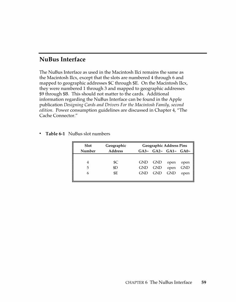
NuBus Interface
The NuBus Interface as used in the Macintosh IIci remains the same asthe Macintosh IIcx, except that the slots are numbered 4 through 6 andmapped to geographic addresses $C through $E. On the Macintosh IIcx,they were numbered 1 through 3 and mapped to geographic addresses$9 through $B. This should not matter to the cards. Additionalinformation regarding the NuBus Interface can be found in the Applepublication Designing Cards and Drivers For the Macintosh Family, secondedition. Power consumption guidelines are discussed in Chapter 4, “TheCache Connector.”
• Table 6-1 NuBus slot numbers
Slot Geographic Geographic Address PinsNumber Address GA3~ GA2~ GA1~ GA0~
4 $C GND GND open open5 $D GND GND open GND6 $E GND GND GND open

60 Developer Notes

61
Appendix A RAM and ROM TimingDiagrams
Timing diagrams for the RAM and ROM signals areprovided in this appendix.

62 Developer Notes

APPENDIX A RAM and ROM Timing Diagrams 63
The following waveforms are idealized drawings of the RAM and ROMinterfaces. The “s” numbers refer to the MC68030 states, while the largenumbers refer to the MDU states. The timings are referenced to theCPUCLK. Both the rising and falling edges of the CPUCLK are used tochange states.
• Figure A-1 RAM burst read timing
s0 s2 s4 s6 s8 s10 s12s1 s3 s5 s7 s9 s11 s13 s14 s15 s16 s17 s18 s19 s20 s21 s0 s1 s2 s3
0 2 4 6 8 101 3 5 7 9 11 12 13 14 15 16 17 18 19 20 21 0
7 98 0 Read or Write:0 1
Burst Read:
Read:
End of Proceeding RAM read
Start of another RAM read or write
RAM (80 ns fast page mode)25 MHz 68030 burst read5 clock minimum initial access, 2 clock subsequent accesses
CPUCLX
Address Bus
AS-
Data Bus
STERM-
CBREQ
CBACK
R/W

64 Developer Notes
• Figure A-2 RAM random read timing
s0 s2 s4 s6 s8 s10 s0s1 s3 s5 s7 s9 s11 s1 s2 s3 s4 s5 s6 s7 s8 s9 s0 s1 s2 s3
2 4 6 8 01 3 5 7 9
5 76 8 0 1
Read:
Read:
s4
9 0 Read: 0 1
0
2 3 4 5 6 7 8 9
0 1 2Read or Write:
End of Proceeding RAM read
Start of another RAM read or write
RAM (80 ns fast page mode)25 MHz 68030 burst read5 clock minimum initial access, 2 clock subsequent accesses
CPUCLX
Address Bus
AS-
Data Bus
STERM-
CBREQ
CBACK
R/W
• Figure A-3 RAM random write timing
s0 s1 s2 s3 s6 s7 s0 s1 s2
6 7 8 02 40 51s3 s4 s5s4
3s5
2 41
s6 s7
6
s8 s9
9s0 s1 s2
3 5 7 8
s3
9
RAM (80 ns fast page mode)25 MHz 68030 random write4 clock minimum access
5 clock access (delayed by previous write cyc
CPUCLK
Address Bu
AS~
STERM~
CBREQ~
CBACK~
R/W~
Data Bus
8 97 0Read:Write
End ofpreceding
RAMread
0Write
s4 s5
0Read or Writ 0 1
Start ofanother
RAM reador write

APPENDIX A RAM and ROM Timing Diagrams 65
• Figure A-4 RAM refresh timing
s0 s2s1 s3 s4(0) 1 2 3 4 5 6 8 9 10 11 07
5 6 7 8 (9 0)
Refresh:
Write: Read: 0 1 2
End of RAM write cycle
Continuation of held-off 68030 RAM read or write cycle
RAM (80 ns fast page mode)25 MHz RAM refresh cycle6 clock cycle every 15.6µS (refresh cycle can overlap previous RAM cycle by 1 clock; next RAM cycle may be held off for 5 clocks by refresh cycle)
Start of a new 68030 RAM cycle
Start of RAM refresh cycle
CPUCLX
Address Bus
Data Bus
STERM~
CBREQ~
CBACK~
R/W~
• Figure A-5 ROM read timing
s0 s2s10 0 0 1 2 3 4 6 0 0 0 05
CPUCLX
Address Bus
Data Bus
STERM~
s1 s2 s3 s4 s5 s6 s8 s9s7 s0 s1
AS~
25 MHz 68030 ROM read5 clock access


67
Appendix B Diagnostic Pinouts
Additional signals are provided for Apple’s internal use indebugging and for emulator support. These signals aredocumented in this chapter for developers to use todevelop emulators and other hardware debugging tools.

68 Developer Notes
APPENDIX A RAM and ROM Timing Diagrams 69
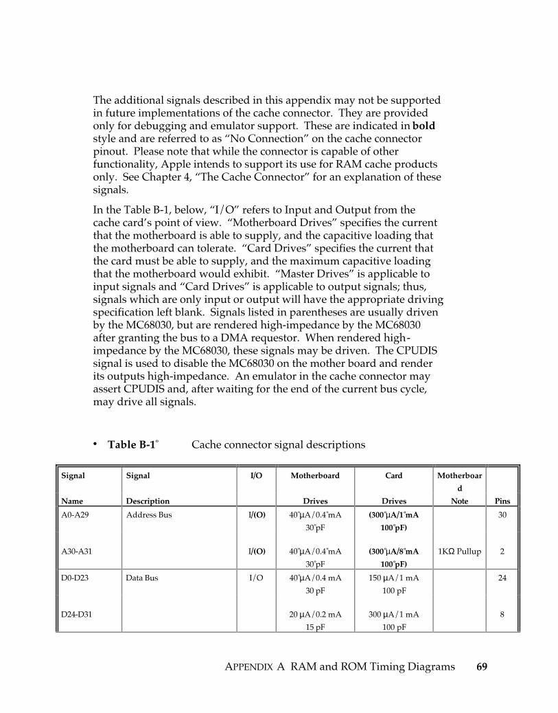
The additional signals described in this appendix may not be supportedin future implementations of the cache connector. They are providedonly for debugging and emulator support. These are indicated in boldstyle and are referred to as “No Connection” on the cache connectorpinout. Please note that while the connector is capable of otherfunctionality, Apple intends to support its use for RAM cache productsonly. See Chapter 4, “The Cache Connector” for an explanation of thesesignals.
In the Table B-1, below, “I/O” refers to Input and Output from thecache card’s point of view. “Motherboard Drives” specifies the currentthat the motherboard is able to supply, and the capacitive loading thatthe motherboard can tolerate. “Card Drives” specifies the current thatthe card must be able to supply, and the maximum capacitive loadingthat the motherboard would exhibit. “Master Drives” is applicable toinput signals and “Card Drives” is applicable to output signals; thus,signals which are only input or output will have the appropriate drivingspecification left blank. Signals listed in parentheses are usually drivenby the MC68030, but are rendered high-impedance by the MC68030after granting the bus to a DMA requestor. When rendered high-impedance by the MC68030, these signals may be driven. The CPUDISsignal is used to disable the MC68030 on the mother board and renderits outputs high-impedance. An emulator in the cache connector mayassert CPUDIS and, after waiting for the end of the current bus cycle,may drive all signals.
• Table B-1 Cache connector signal descriptions
Signal Signal I/O Motherboard Card Motherboar
d
Name Description Drives Drives Note Pins
A0-A29 Address Bus I/(O) 40 µA/0.4 mA
30 pF
(300 µA/1 mA
100 pF)
30
A30-A31 I/(O) 40 µA/0.4 mA
30 pF
(300 µA/8 mA
100 pF)
1KΩ Pullup 2
D0-D23 Data Bus I/O 40 µA/0.4 mA
30 pF
150 µA/1 mA
100 pF
24
D24-D31 20 µA/0.2 mA
15 pF
300 µA/1 mA
100 pF
8

70 Developer Notes
RESET~ Reset I/O 20 µA/0.2 mA
15 pF
N.A./15 mA
50 pF
Open
Collector
470Ω pullup
1
BERR~ Bus Error I/O 40 µA/0.4 mA
30 pF
100 µA/8 mA
50 pF
1 KΩ pullup 1
HALT~ Halt I/O 40 µA/0.4 mA
30 pF
100 µA/8 mA
50 pF
1 KΩ pullup 1
FC0-FC2 Function Codes I/(O) 20 µA/0.2 mA
15 pF
(100 µA/8 mA
50 pF)
1 KΩ pullup 3
BR~ Bus Request I 40 µA/0.4 mA
30 pF
1 KΩpullup
1
BG~ Bus Grant I/(O) 40 µA/0.4 mA
30 pF
(100 µA/8 mA
50 pF)
1 KΩ pullup 1
BGACK~ Bus Grant Acknowledge I 40 µA/0.4 mA
30 pF
1
SIZ0-SIZ1 Transfer Size I/(O) 40 µA/0.4 mA
30 pF
(40 µA/0.4 mA
30 pF)
2
AS~ Address Strobe I/(O) 40 µA/0.4 mA
30 pF
(300 µA/8 mA
100 pF)
1 KΩ pullup 1
DSACK0~,
DSACK1~
Data Transfer and Size
Acknowledge
I/O 40 µA/0.4 mA
30 pF
100 µA/8 mA
50 pF
1 KΩpullup
2
R/W~ Read/Write I/(O) 40 µA/0.4 mA
30 pF
(300 µA/8 mA
100 pF)
1 KΩ pullup 1
STERM~ Synchronous Termination I/O 40 µA/0.4 mA
30 pF
100 µA/8 mA
50 pF
1 KΩ pullup 1
CBACK~ Cache Burst Acknowledge I/O 40 µA/0.4 mA
30 pF
100 µA/8 mA
50 pF
1 KΩ pullup 1
CBREQ~ Cache Burst Request I/(O) 40 µA/0.4 mA
30 pF
(100 µA/8 mA
50 pF)
1 KΩ pullup 1
CIOUT~ Cache Inhibit Out I/(O) 40 µA/0.4 mA
30 pF
(100 µA/8 mA
50 pF)
1 KΩ pullup 1
DS~ Data Strobe I/(O) 40 µA/0.4 mA
30 pF
(100 µA/8 mA
50 pF)
1 KΩ pullup 1
RMC~ Read Modify write Cycle I/(O) 40 µA/0.4 mA
30 pF
(100 µA/8 mA
50 pF)
1 KΩ pullup 1
IPL0~-IPL2~ Interrupt Priority Lines I 40 µA/0.4 mA
30 pF
1 KΩpullup
3
CPUCLK CPU Clock (25 MHz) I 10µA/10µA
15 pF
1
ROMOE~ ROM Output Enable I 40 µA/0.4 mA
30 pF
1
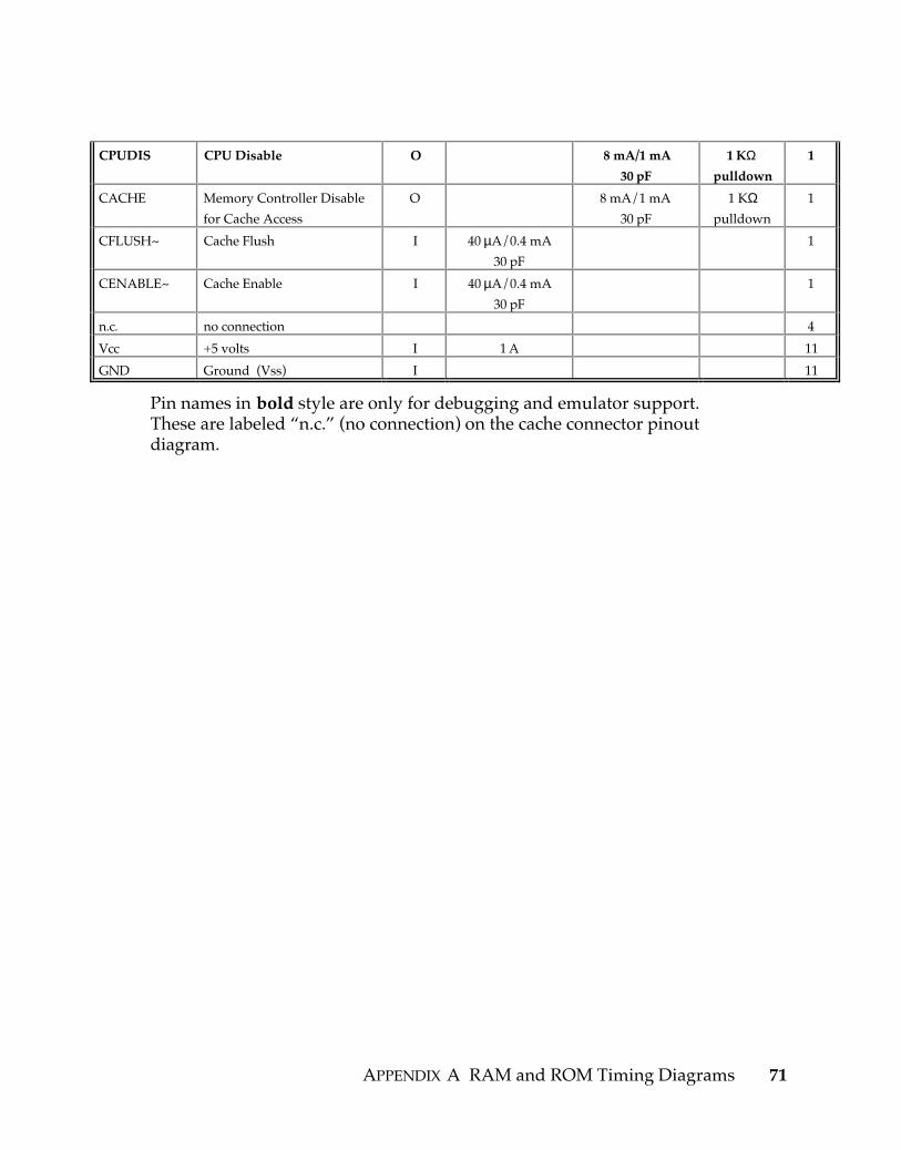
APPENDIX A RAM and ROM Timing Diagrams 71
CPUDIS CPU Disable O 8 mA/1 mA
30 pF
1 KΩpulldown
1
CACHE Memory Controller Disable
for Cache Access
O 8 mA/1 mA
30 pF
1 KΩpulldown
1
CFLUSH~ Cache Flush I 40 µA/0.4 mA
30 pF
1
CENABLE~ Cache Enable I 40 µA/0.4 mA
30 pF
1
n.c. no connection 4
Vcc +5 volts I 1 A 11
GND Ground (Vss) I 11
Pin names in bold style are only for debugging and emulator support.These are labeled “n.c.” (no connection) on the cache connector pinoutdiagram.
72 Developer Notes
• Figure B-1 Cache connector pinout diagram
A B CA30 1 RESET~ 1 R/W~
HALT~ 2 A29 2 STERM~A31 3 A25 3 A28A26 4 A27 4 Vcc
RMC~ 5 A24 5 CFLUSH~D31 6 GND 6 VccD30 7 D29 7 n.c.D28 8 D27 8 GNDD26 9 D25 9 VccD24 10 D23 10 GNDD22 11 D21 11 GNDD20 12 D19 12 IPL2~D18 13 D17 13 CENABLE~D16 14 Vcc 14 VccA22 15 A21 15 VccA20 16 A19 16 GNDA18 17 A17 17 n.c.A16 18 A15 18 GNDA14 19 A13 19 VccA12 20 A11 20 n.c.A10 21 GND 21 GNDFC1 22 A9 22 VccA8 23 n.c. 23 GNDFC2 24 FC0 24 CIOUT~D15 25 D14 25 IPL1~D13 26 D12 26 IPL0~D11 27 D10 27 CBREQ~D9 28 D8 28 D7D6 29 BGACK~ 29 D5D4 30 D3 30 D2D1 31 D0 31 Vcc
ROMOE~ 32 A7 32 A6A5 33 A4 33 A3A2 34 A1 34 A0
BG~ 35 Vcc 35 CBACK~A23 36 CPUDIS 36 BR~
DSACK0~ 37 AS~ 37 DS~CPUCLK 38 DSACK1~ 38 BERR~
GND 39 Vcc 39 SIZ1GND 40 CACHE 40 SIZ0

APPENDIX A RAM and ROM Timing Diagrams 73
• Table B-2 Cache connector pin diagramA B C
A30HALT~A31A26RMC~D31D30D28D26D24D22D20D18D16A22A20A18A16A14A12A10FC1A8FC2D15D13D11D9D6D4D1ROMOE~A5A2BG~A23DSACK0~CPUCLKGNDGND
RESET~A29A25A27A24GNDD29D27D25D23D21D19D17VccA21A19A17A15A13A11GNDA9n.c.FC0D14D12D10D8BGACK~D3D0A7A4A1VccCPUDISAS~DSACK1~VccCACHE
R/W~STERM~A28VccCFLUSH~Vccn.c.GNDVccGndGndIPL2~CENABLE~VccVccGNDn.c.GNDVccn.c.GNDVccGNDCIOUT~IPL1~IPL0~CBREQ~D7D5D2VccA6A3A0CBACK~BR~DS~BERR~SIZ1SIZ0
12345678910111213141516171819202122232425262728293031323334353637383940
123456789
10111213141516171819202122232425262728293031323334353637383940


75
Appendix C Cache signal timing diagrams
The cache card connector signal timing diagrams areprovided in this appendix.

76 Developer Notes

APPENDIX C Cache signal timing diagrams 77
• Figure C-1 Timing diagram showing the interaction betweencache card signals and the optional Parity Generator Chip
CPU
Clo
ck
STE
RM
~
CA
CH
E
No
pari
ty
erro
r he
re,
even
thou
gh
STE
RM
~=0
at p
revi
ous
risi
ng e
dge
of c
lock
and
C
AC
HE
=0
at th
is e
dge,
be
caus
e va
lid
DR
AM
dat
a is
pre
sent
No
pari
ty
erro
r he
re
beca
use
STE
RM
~=1
at p
revi
ous
risi
ng e
dge
of c
lock
No
pari
ty
erro
r he
re
beca
use
CA
CH
E=
1 at
this
fa
lling
edg
e of
clo
ck
No
pari
ty
erro
r he
re
beca
use
CA
CH
E=
1 at
pre
viou
s fa
lling
edg
e of
clo
ck
No
pari
ty
erro
r he
re
beca
use
STE
RM
~=1
at p
revi
ous
risi
ng e
dge
of c
lock
No
pari
ty
erro
r he
re
beca
use
STE
RM
~=1
at p
revi
ous
risi
ng e
dge
of c
lock
Pari
ty e
rror
he
re b
ecau
se
STE
RM
~=0
at p
revi
ous
risi
ng e
dge
of c
lock
, C
AC
HE
=0
at th
is e
dge,
an
d va
lid
DR
AM
dat
a is
not
pre
sent
(s
ee N
ote
2)
No
pari
ty
erro
r he
re
beca
use
CA
CH
E=
1 at
this
fa
lling
edg
e of
clo
ck
No
pari
ty
erro
r he
re
beca
use
CA
CH
E=
1 at
pre
viou
s fa
lling
edg
e of
clo
ck
STE
RM
~=0
at p
revi
ous
risi
ng e
dge
of c
lock
, C
AC
HE
=0
at th
is e
dge,
an
d va
lid
DR
AM
dat
a is
not
pre
sent
(s
ee N
ote
2)
No
pari
ty
erro
r he
re
beca
use
STE
RM
~=1
at p
revi
ous
risi
ng e
dge
of c
lock
DR
AM
Rea
dG
ood
Cac
he C
ard
Rea
dB
ad C
ache
Car
d R
ead
Not
e 1:
The
cyc
les
show
n in
this
dia
gram
are
mea
nt to
sho
w v
ario
us p
ossi
ble
rela
tive
timin
gs o
f ST
ER
M~
and
C
AC
HE
, as
they
affe
ct p
arity
che
ckin
g in
a M
acin
tosh
IIci
with
par
ity o
ptio
n. T
hese
cyc
les
do n
ot r
epre
sent
ac
tual
Mac
into
sh II
ci D
RA
M o
r ca
che
card
cyc
les.
Not
e 2:
In a
Mac
into
sh II
ci w
ith p
arity
opt
ion,
a p
arity
err
or m
ay o
ccur
if S
TE
RM
~ is
low
at a
ny r
isin
g ed
ge
of C
PU
clo
ck u
nles
s:
1) v
alid
DR
AM
dat
a is
pre
sent
at t
he n
ext f
allin
g ed
ge, o
r 2)
CA
CH
E is
hig
h at
the
next
falli
ng e
dge,
or
3) C
AC
HE
was
hig
h at
the
prev
ious
falli
ng e
dge.
Not
e 3:
Par
ity e
rror
s ar
e no
t gen
erat
ed fo
r w
rites
, for
acc
esse
s ou
tsid
e of
the
DR
AM
phy
sica
l add
ress
spa
ce
($00
00 0
000
thro
ugh
$07F
F F
FF
F),
or
whe
n pa
rity
chec
king
is d
isab
led.

78 Developer Notes
• Figure C-2 Timing diagram showing the interaction between ageneric cache card’s signals and the Macintosh IIci’sNuBus connector signals
CPU
Clo
ck
AS~
End
of
NuB
us D
RA
M R
ead
Cac
he R
ead
Mac
IIc
i ST
ER
M E
nabl
e~
Mac
IIc
iST
ER
M~
Cac
he C
ard
STE
RM
~
Cac
he C
ard
R/W
NuB
us C
ontr
olle
r A
S~
6803
0A
S~
Star
t of
DR
AM
Rea
d by
NuB
us M
aste
r
Mac
IIc
iST
ER
M~
Mac
IIc
i ST
ER
M E
nabl
e~
Bus
Acq
uisi
tion
by N
uBus
NuB
us C
ontr
olle
r A
S~
NuB
us C
ontr
olle
r B
GA
CK
~ N
uBus
Con
trol
ler
BG
AC
K~
NuB
us C
ontr
olle
r B
GA
CK
Ena
ble~
N
uBus
Con
trol
ler
BG
AC
K E
nabl
e~
Bus
Rel
ease
by
NuB
us
(wai
ts f
or N
uBus
AC
K*)
BG
~
BR
~N
uBus
Con
trol
ler
BR
~
6803
0A
S~
Cac
he R
ead
(See
Not
e 2)
(See
Not
e 2)
(See
Not
e 2)
(See
Not
e 2)
Not
e 1:
The
tran
sitio
ns in
dica
ted
for
cach
e ca
rd s
igna
ls S
TE
RM
~ a
nd C
AC
HE
sho
w th
e ra
nge
of a
ccep
tabl
e tr
ansi
tion
times
that
will
allo
w th
e fa
stes
t pos
sibl
e op
erat
ion
of th
e co
mpu
ter
and
the
cach
e. T
rans
ition
s ou
tsid
e of
thes
e ra
nges
may
cau
se v
ario
us s
orts
of e
rror
s or
con
tent
ion,
or
may
del
ay th
e ac
cess
that
fo
llow
s.N
ote
2: In
the
Mac
into
sh II
ci w
ith p
arity
opt
ion,
a p
arity
err
or m
ay o
ccur
if S
TE
RM
~ is
low
at a
ny r
isin
g ed
ge
of C
PU
clo
ck u
nles
s:1)
val
id D
RA
M d
ata
is p
rese
nt a
t the
nex
t fal
ling
edge
, or
2) C
AC
HE
is h
igh
at th
e ne
xt fa
lling
edg
e, o
r3)
C
AC
HE
was
hig
h at
the
prev
ious
falli
ng e
dge.

APPENDIX C Cache signal timing diagrams 79
• Figure C-3 Timing diagram showing the interaction between ageneric cache card and the Macintosh IIci
CPU
Clo
ck
AS~
STE
RM
~
CA
CH
E
End
of
DR
AM
Rea
d C
ache
Rea
d C
ache
Rea
d M
iss
(Ret
ry)
Star
t of
DR
AM
Rea
d R
etry
BE
RR
~,
HA
LT
~
Ret
ry R
ecov
ery
Tim
e
Mac
IIc
i ST
ER
M E
nabl
e~
Mac
IIc
i ST
ER
M~
Cac
he C
ard
STE
RM
~
Cac
he
Car
d
(See
Not
e 2)
(See
Not
e 2)
Cac
he C
ard
R/W
Not
e1: T
he tr
ansi
tions
indi
cate
d fo
r ca
che
card
sig
nals
ST
ER
M~
, CA
CH
E, B
ER
R~
, and
HA
LT s
how
the
rang
e of
ac
cept
able
tran
sitio
n tim
es h
tat w
ill a
llow
the
fast
est p
ossi
ble
oper
atio
n of
the
com
pute
r an
d th
e ca
che.
T
rans
ition
s ou
tsid
e of
thes
e ra
nges
may
cau
se v
ario
us s
orts
of e
rror
s or
con
tent
ion,
or
may
del
ay th
e ac
cess
that
follo
ws.
Not
e 2:
A fa
lse
parit
y er
ror
may
occ
ur a
fter
a ca
che
card
acc
ess
if S
TE
RM
~ is
not
driv
en h
igh
befo
re th
e ris
ing
cloc
k ed
ge th
at fo
llow
s th
e fir
st fa
lling
edg
e af
ter
the
CA
CH
E s
igna
l is
driv
en lo
w.

80 Developer Notes
• Figure C-4 Timing diagram showing the interaction between ageneric cache card’s signals and the Macintosh IIci NuBus’signals
CPU
Clo
ck
AS~
STE
RM
~
CA
CH
E
End
of
DR
AM
Wri
te
Cac
he R
ead
DR
AM
Wri
te
BE
RR
~,
HA
LT
~
Mac
IIc
i ST
ER
M E
nabl
e~
Mac
IIc
i ST
ER
M~
Cac
he C
ard
STE
RM
~
Cac
he C
ard
Mac
IIc
i ST
ER
M~
Mac
IIc
i ST
ER
M E
nabl
e~
Cac
he R
ead
R/W
(See
Not
e 2)
Not
e1: T
he tr
ansi
tions
indi
cate
d fo
r ca
che
card
sig
nals
ST
ER
M~
, CA
CH
E, B
ER
R~
, and
HA
LT s
how
the
rang
e of
ac
cept
able
tran
sitio
n tim
es h
tat w
ill a
llow
the
fast
est p
ossi
ble
oper
atio
n of
the
com
pute
r an
d th
e ca
che.
T
rans
ition
s ou
tsid
e of
thes
e ra
nges
may
cau
se v
ario
us s
orts
of e
rror
s or
con
tent
ion,
or
may
del
ay th
e ac
cess
that
follo
ws.
Not
e 2:
Thi
s tim
ing
diag
ram
illu
stra
tes
the
effe
ct o
f writ
es (
R/W
=0)
on
a ca
che
card
. T
he e
ffect
of
cach
e-in
hibi
ted
acce
sses
(C
IOU
T~
=0)
and
cop
roce
ssor
acc
esse
s (F
CO
-2=
111)
_ fo
llow
sim
ilar
timin
g.F
igur
e B
-5 is
a c
ompl
ete
pino
ut d
iagr
am a
nd is
pro
vide
d on
ly fo
r us
e w
ith e
mul
ator
s an
d te
ster
s.

THE APPLE PUBLISHINGSYSTEM
This Apple manual waswritten, edited, andcomposed on a desktoppublishing system usingApple Macintosh®
computers andMicrosoft® Wordsoftware. Proof and finalpages were created on theApple LaserWriter®
printers. Line art wascreated using AdobeIllustrator™.POSTSCRIPT®, the page-description language forthe LaserWriter, wasdeveloped by AdobeSystems Incorporated.Text type and displaytype are Apple’scorporate font, acondensed version ofGaramond. Bullets areITC Zapf Dingbats® .Some elements, such asprogram listings, are setin Apple Courier.