MachXO2™ Family Data Sheet - Farnell element14 · March 2012 Data Sheet DS1035 ... and...
103
MachXO2™ Family Data Sheet DS1035 Version 01.9, April 2012
Transcript of MachXO2™ Family Data Sheet - Farnell element14 · March 2012 Data Sheet DS1035 ... and...
MachXO2™ Family Data Sheet
DS1035 Version 01.9, April 2012
www.latticesemi.com 1-1 DS1035 Introduction_01.5
March 2012 Data Sheet DS1035
© 2012 Lattice Semiconductor Corp. All Lattice trademarks, registered trademarks, patents, and disclaimers are as listed at www.latticesemi.com/legal. All other brand or product names are trademarks or registered trademarks of their respective holders. The specifications and information herein are subject to change without notice.
Features Flexible Logic Architecture
• Six devices with 256 to 6864 LUT4s and 19 to 335 I/Os
Ultra Low Power Devices• Advanced 65 nm low power process• As low as 19 µW standby power • Programmable low swing differential I/Os • Stand-by mode and other power saving options
Embedded and Distributed Memory• Up to 240 Kbits sysMEM™ Embedded Block
RAM• Up to 54 Kbits Distributed RAM• Dedicated FIFO control logic
On-Chip User Flash Memory• Up to 256 Kbits of User Flash Memory• 100,000 write cycles• Accessible through WISHBONE, SPI, I2C and
JTAG interfaces • Can be used as soft processor PROM or as
Flash memory Pre-Engineered Source Synchronous I/O
• DDR registers in I/O cells• Dedicated gearing logic• 7:1 Gearing for Display I/Os• Generic DDR, DDRX2, DDRX4• Dedicated DDR/DDR2/LPDDR memory with
DQS support High Performance, Flexible I/O Buffer
• Programmable sysIO™ buffer supports wide range of interfaces:
– LVCMOS 3.3/2.5/1.8/1.5/1.2– LVTTL– PCI– LVDS, Bus-LVDS, MLVDS, RSDS, LVPECL– SSTL 25/18– HSTL 18– Schmitt trigger inputs, up to 0.5V hysteresis
• I/Os support hot socketing• On-chip differential termination• Programmable pull-up or pull-down mode
Flexible On-Chip Clocking• Eight primary clocks• Up to two edge clocks for high-speed I/O
interfaces (top and bottom sides only)• Up to two analog PLLs per device with
fractional-n frequency synthesis– Wide input frequency range (10 MHz to
400 MHz) Non-volatile, Infinitely Reconfigurable
• Instant-on – powers up in microseconds• Single-chip, secure solution• Programmable through JTAG, SPI or I2C• Supports background programming of non-vola-
tile memory• Optional dual boot with external SPI memory
TransFR™ Reconfiguration • In-field logic update while system operates
Enhanced System Level Support• On-chip hardened functions: SPI, I2C, timer/
counter• On-chip oscillator with 5.5% accuracy• Unique TraceID for system tracking• One Time Programmable (OTP) mode• Single power supply with extended operating
range• IEEE Standard 1149.1 boundary scan• IEEE 1532 compliant in-system programming
Broad Range of Package Options• TQFP, WLCSP, ucBGA, csBGA, caBGA, ftBGA,
fpBGA, QFN package options• Small footprint package options
– As small as 2.5x2.5mm• Density migration supported• Advanced halogen-free packaging
MachXO2 Family Data SheetIntroduction

1-2
IntroductionMachXO2 Family Data Sheet
Table 1-1. MachXO2™ Family Selection Guide
IntroductionThe MachXO2 family of ultra low power, instant-on, non-volatile PLDs has six devices with densities ranging from 256 to 6864 Look-Up Tables (LUTs). In addition to LUT-based, low-cost programmable logic these devices feature Embedded Block RAM (EBR), Distributed RAM, User Flash Memory (UFM), Phase Locked Loops (PLLs), pre-engineered source synchronous I/O support, advanced configuration support including dual-boot capability and hardened versions of commonly used functions such as SPI controller, I2C controller and timer/counter. These fea-tures allow these devices to be used in low cost, high volume consumer and system applications.
The MachXO2 devices are designed on a 65nm non-volatile low power process. The device architecture has sev-eral features such as programmable low swing differential I/Os and the ability to turn off I/O banks, on-chip PLLs
XO2-256 XO2-640 XO2-640U1 XO2-1200 XO2-1200U1 XO2-2000 XO2-2000U1 XO2-4000 XO2-7000
LUTs 256 640 640 1280 1280 2112 2112 4320 6864
Distributed RAM (Kbits) 2 5 5 10 10 16 16 34 54
EBR SRAM (Kbits) 0 18 64 64 74 74 92 92 240
Number of EBR SRAMBlocks (9 Kbits/block)
Device Options
0 2 7 7 8 8 10 10 26
UFM (Kbits) 0
✓
✓
✓
✓
✓ ✓
✓
✓✓✓
✓✓
✓✓✓
✓✓✓
✓24 64 64 80 80 96 96 256
Number of PLLs
Packages I/Os
0
HC2
HE3
ZE4
0 1 1 1 1 2 2 2Hardened Functions: I2CSPITimer/Counter
211
211
211
211
211
211
211
211
211
25 WLCSP5
(2.5 x 2.5mm, 0.4mm)
32 QFN6
(5 x 5mm, 0.5mm)
19
64 ucBGA (4 x 4mm, 0.4mm)
45
22
100 TQFP (14 x 14mm)
132 csBGA (8 x 8mm, 0.5mm)
144 TQFP (20 x 20mm)
256 caBGA (14 x 14mm, 0.8mm)
256 ftBGA (17 x 17mm, 1.0mm)
332 caBGA (17 x 17mm, 0.8mm)
484 fpBGA (23 x 23mm, 1.0mm)
1. Ultra high I/O device.2. High performance with regulator – VCC = 2.5V, 3.3V 3. High performance without regulator – VCC = 1.2V 4. Low power without regulator – VCC = 1.2V 5. WLCSP package only available for ZE devices.6. QFN package only available for HC and ZE devices.
207
279 279 335
275 279
207207 207 207
207 207 207
108 108 112 115 115
56 80 105 105 105
56 79 80 80

1-3
IntroductionMachXO2 Family Data Sheet
and oscillators dynamically. These features help manage static and dynamic power consumption resulting in low static power for all members of the family.
The MachXO2 devices are available in two versions – ultra low power (ZE) and high performance (HC and HE) devices. The ultra low power devices are offered in three speed grades -1, -2 and -3, with -3 being the fastest. Sim-ilarly, the high-performance devices are offered in three speed grades: -4, -5 and -6, with -6 being the fastest. HC devices have an internal linear voltage regulator which supports external VCC supply voltages of 3.3V or 2.5V. ZE and HE devices only accept 1.2V as the external VCC supply voltage. With the exception of power supply voltage all three types of devices (ZE, HC and HE) are functionally compatible and pin compatible with each other.
The MachXO2 PLDs are available in a broad range of advanced halogen-free packages ranging from the space saving 2.5x2.5 mm WLCSP to the 23x23 mm fpBGA. MachXO2 devices support density migration within the same package. Table 1-1 shows the LUT densities, package and I/O options, along with other key parameters.
The pre-engineered source synchronous logic implemented in the MachXO2 device family supports a broad range of interface standards, including LPDDR, DDR, DDR2 and 7:1 gearing for display I/Os.
The MachXO2 devices offer enhanced I/O features such as drive strength control, slew rate control, PCI compati-bility, bus-keeper latches, pull-up resistors, pull-down resistors, open drain outputs and hot socketing. Pull-up, pull-down and bus-keeper features are controllable on a “per-pin” basis.
A user-programmable internal oscillator is included in MachXO2 devices. The clock output from this oscillator may be divided by the timer/counter for use as clock input in functions such as LED control, key-board scanner and sim-ilar state machines.
The MachXO2 devices also provide flexible, reliable and secure configuration from on-chip Flash memory. These devices can also configure themselves from external SPI Flash or be configured by an external master through the JTAG test access port or through the I2C port. Additionally, MachXO2 devices support dual-boot capability (using external Flash memory) and remote field upgrade (TransFR) capability.
Lattice provides a variety of design tools that allow complex designs to be efficiently implemented using the MachXO2 family of devices. Popular logic synthesis tools provide synthesis library support for MachXO2. Lattice design tools use the synthesis tool output along with the user-specified preferences and constraints to place and route the design in the MachXO2 device. These tools extract the timing from the routing and back-annotate it into the design for timing verification.
Lattice provides many pre-engineered IP (Intellectual Property) LatticeCORE™ modules, including a number of reference designs licensed free of charge, optimized for the MachXO2 PLD family. By using these configurable soft core IP cores as standardized blocks, users are free to concentrate on the unique aspects of their design, increas-ing their productivity.
www.latticesemi.com 2-1 DS1035 Architecture_01.4
April 2012 Data Sheet DS1035
© 2012 Lattice Semiconductor Corp. All Lattice trademarks, registered trademarks, patents, and disclaimers are as listed at www.latticesemi.com/legal. All other brand or product names are trademarks or registered trademarks of their respective holders. The specifications and information herein are subject to change without notice.
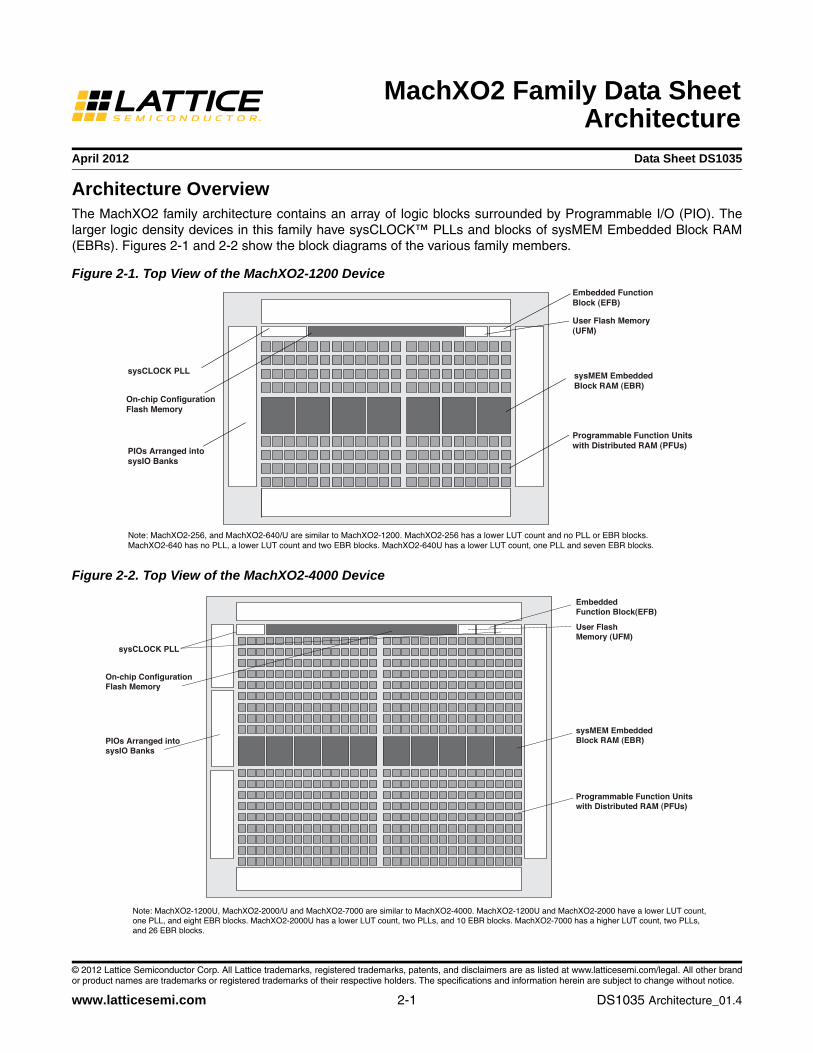
Architecture OverviewThe MachXO2 family architecture contains an array of logic blocks surrounded by Programmable I/O (PIO). The larger logic density devices in this family have sysCLOCK™ PLLs and blocks of sysMEM Embedded Block RAM (EBRs). Figures 2-1 and 2-2 show the block diagrams of the various family members.
Figure 2-1. Top View of the MachXO2-1200 Device
Figure 2-2. Top View of the MachXO2-4000 Device
sysMEM EmbeddedBlock RAM (EBR)
sysCLOCK PLL
PIOs Arranged intosysIO Banks
Programmable Function Unitswith Distributed RAM (PFUs)
Embedded FunctionBlock (EFB)
User Flash Memory(UFM)
On-chip ConfigurationFlash Memory
Note: MachXO2-256, and MachXO2-640/U are similar to MachXO2-1200. MachXO2-256 has a lower LUT count and no PLL or EBR blocks. MachXO2-640 has no PLL, a lower LUT count and two EBR blocks. MachXO2-640U has a lower LUT count, one PLL and seven EBR blocks.
sysMEM EmbeddedBlock RAM (EBR)
Programmable Function Unitswith Distributed RAM (PFUs)
On-chip ConfigurationFlash Memory
sysCLOCK PLL
PIOs Arranged intosysIO Banks
EmbeddedFunction Block(EFB)
User FlashMemory (UFM)
Note: MachXO2-1200U, MachXO2-2000/U and MachXO2-7000 are similar to MachXO2-4000. MachXO2-1200U and MachXO2-2000 have a lower LUT count, one PLL, and eight EBR blocks. MachXO2-2000U has a lower LUT count, two PLLs, and 10 EBR blocks. MachXO2-7000 has a higher LUT count, two PLLs, and 26 EBR blocks.
MachXO2 Family Data SheetArchitecture
2-2
ArchitectureMachXO2 Family Data Sheet
The logic blocks, Programmable Functional Unit (PFU) and sysMEM EBR blocks, are arranged in a two-dimen-sional grid with rows and columns. Each row has either the logic blocks or the EBR blocks. The PIO cells are located at the periphery of the device, arranged in banks. The PFU contains the building blocks for logic, arithmetic, RAM, ROM, and register functions. The PIOs utilize a flexible I/O buffer referred to as a sysIO buffer that supports operation with a variety of interface standards. The blocks are connected with many vertical and horizontal routing channel resources. The place and route software tool automatically allocates these routing resources.
In the MachXO2 family, the number of sysIO banks varies by device. There are different types of I/O buffers on the different banks. Refer to the details in later sections of this document. The sysMEM EBRs are large, dedicated fast memory blocks; these blocks are found in MachXO2-640/U and larger devices. These blocks can be configured as RAM, ROM or FIFO. FIFO support includes dedicated FIFO pointer and flag “hard” control logic to minimize LUT usage.
The MachXO2 architecture also provides up to two sysCLOCK Phase Locked Loop (PLL) blocks on MachXO2-640U, MachXO2-1200/U and larger devices. These blocks are located at the ends of the on-chip Flash block. The PLLs have multiply, divide, and phase shifting capabilities that are used to manage the frequency and phase rela-tionships of the clocks.
MachXO2 devices provide commonly used hardened functions such as SPI controller, I2C controller and timer/counter. MachXO2-640/U and higher density devices also provide User Flash Memory (UFM). These hardened functions and the UFM interface to the core logic and routing through a WISHBONE interface. The UFM can also be accessed through the SPI, I2C and JTAG ports.
Every device in the family has a JTAG port that supports programming and configuration of the device as well as access to the user logic. The MachXO2 devices are available for operation from 3.3V, 2.5V and 1.2V power sup-plies, providing easy integration into the overall system.
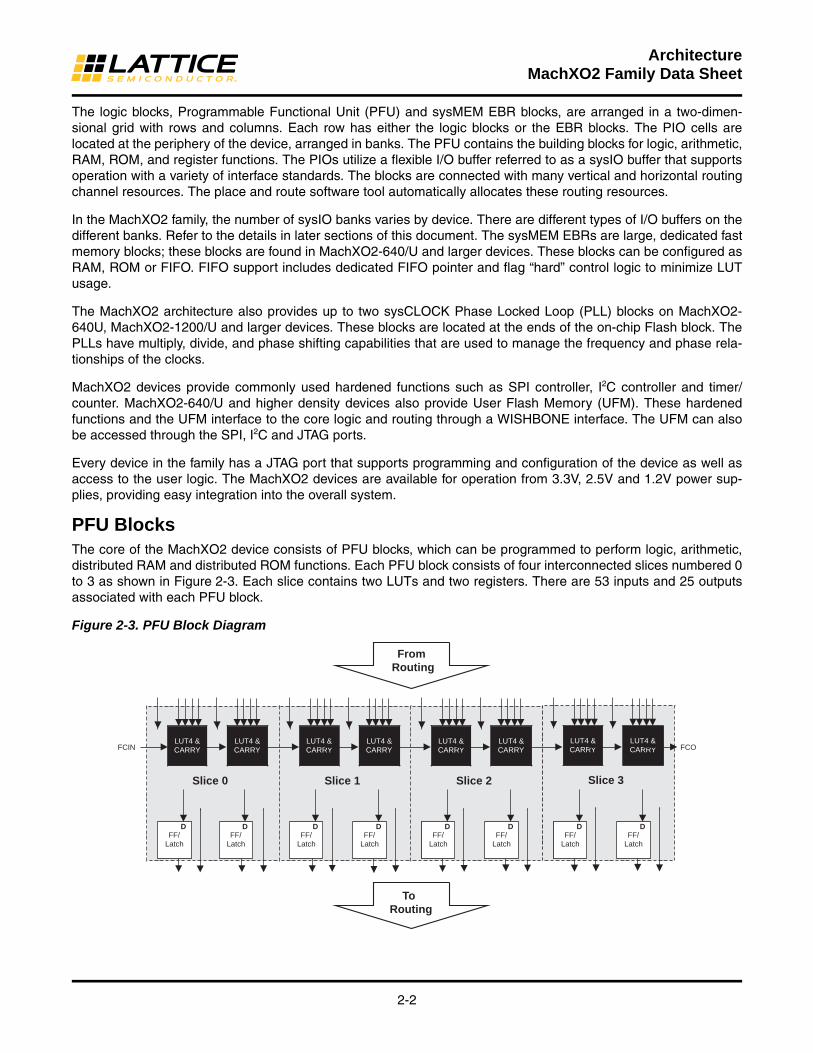
PFU BlocksThe core of the MachXO2 device consists of PFU blocks, which can be programmed to perform logic, arithmetic, distributed RAM and distributed ROM functions. Each PFU block consists of four interconnected slices numbered 0 to 3 as shown in Figure 2-3. Each slice contains two LUTs and two registers. There are 53 inputs and 25 outputs associated with each PFU block.
Figure 2-3. PFU Block Diagram
Slice 0
LUT4 & CARRY
LUT4 & CARRY
FF/ Latch
FCIN FCO
D FF/
Latch
D
Slice 1
LUT4 & CARRY
LUT4 & CARRY
Slice 2
LUT4 & CARRY
LUT4 & CARRY
From Routin g
To Routin g
Slice 3
LUT4 & CARRY
LUT4 & CARRY
FF/ Latch
D FF/
Latch
D FF/
Latch
D FF/
Latch
D FF/
Latch
D FF/
Latch
D
2-3
ArchitectureMachXO2 Family Data Sheet
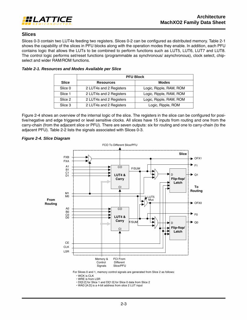
SlicesSlices 0-3 contain two LUT4s feeding two registers. Slices 0-2 can be configured as distributed memory. Table 2-1 shows the capability of the slices in PFU blocks along with the operation modes they enable. In addition, each PFU contains logic that allows the LUTs to be combined to perform functions such as LUT5, LUT6, LUT7 and LUT8. The control logic performs set/reset functions (programmable as synchronous/ asynchronous), clock select, chip-select and wider RAM/ROM functions.
Table 2-1. Resources and Modes Available per Slice
Figure 2-4 shows an overview of the internal logic of the slice. The registers in the slice can be configured for posi-tive/negative and edge triggered or level sensitive clocks. All slices have 15 inputs from routing and one from the carry-chain (from the adjacent slice or PFU). There are seven outputs: six for routing and one to carry-chain (to the adjacent PFU). Table 2-2 lists the signals associated with Slices 0-3.
Figure 2-4. Slice Diagram
Slice
PFU Block
Resources Modes
Slice 0 2 LUT4s and 2 Registers Logic, Ripple, RAM, ROM
Slice 1 2 LUT4s and 2 Registers Logic, Ripple, RAM, ROM
Slice 2 2 LUT4s and 2 Registers Logic, Ripple, RAM, ROM
Slice 3 2 LUT4s and 2 Registers Logic, Ripple, ROM
LUT4 &Carry
Slice
Flip-flop/Latch
OFX0
F0
Q0
CI
CO
LUT4 &Carry
CI
CO
OFX1
F1
Q1
F/SUM
F/SUM D
D
FCI From Different Slice/PFU
Memory &Control Signals
FCO To Different Slice/PFU
LUT5MuxFrom
Routing
ToRouting
For Slices 0 and 1, memory control signals are generated from Slice 2 as follows: • WCK is CLK • WRE is from LSR • DI[3:2] for Slice 1 and DI[1:0] for Slice 0 data from Slice 2 • WAD [A:D] is a 4-bit address from slice 2 LUT input
A0
C0D0
A1B1C1D1
CE
CLK
LSR
M1M0
FXBFXA
B0
Flip-flop/Latch
2-4
ArchitectureMachXO2 Family Data Sheet
Table 2-2. Slice Signal Descriptions
Modes of Operation Each slice has up to four potential modes of operation: Logic, Ripple, RAM and ROM.
Logic Mode In this mode, the LUTs in each slice are configured as 4-input combinatorial lookup tables. A LUT4 can have 16 possible input combinations. Any four input logic functions can be generated by programming this lookup table. Since there are two LUT4s per slice, a LUT5 can be constructed within one slice. Larger look-up tables such as LUT6, LUT7 and LUT8 can be constructed by concatenating other slices. Note LUT8 requires more than four slices.
Ripple Mode Ripple mode supports the efficient implementation of small arithmetic functions. In Ripple mode, the following func-tions can be implemented by each slice:
• Addition 2-bit
• Subtraction 2-bit
• Add/subtract 2-bit using dynamic control
• Up counter 2-bit
• Down counter 2-bit
• Up/down counter with asynchronous clear
• Up/down counter with preload (sync)
• Ripple mode multiplier building block
• Multiplier support
• Comparator functions of A and B inputs – A greater-than-or-equal-to B – A not-equal-to B – A less-than-or-equal-to B
Function Type Signal Names Description
Input Data signal A0, B0, C0, D0 Inputs to LUT4
Input Data signal A1, B1, C1, D1 Inputs to LUT4
Input Multi-purpose M0/M1 Multi-purpose input
Input Control signal CE Clock enable
Input Control signal LSR Local set/reset
Input Control signal CLK System clock
Input Inter-PFU signal FCIN Fast carry in1
Output Data signals F0, F1 LUT4 output register bypass signals
Output Data signals Q0, Q1 Register outputs
Output Data signals OFX0 Output of a LUT5 MUX
Output Data signals OFX1 Output of a LUT6, LUT7, LUT82 MUX depending on the slice
Output Inter-PFU signal FCO Fast carry out1
1. See Figure 2-3 for connection details.2. Requires two PFUs.

2-5
ArchitectureMachXO2 Family Data Sheet
Ripple mode includes an optional configuration that performs arithmetic using fast carry chain methods. In this con-figuration (also referred to as CCU2 mode) two additional signals, Carry Generate and Carry Propagate, are gener-ated on a per-slice basis to allow fast arithmetic functions to be constructed by concatenating slices.
RAM Mode In this mode, a 16x4-bit distributed single port RAM (SPR) can be constructed by using each LUT block in Slice 0 and Slice 1 as a 16x1-bit memory. Slice 2 is used to provide memory address and control signals. A 16x2-bit Pseudo Dual Port RAM (PDPR) memory is created by using one slice as the read-write port and the other compan-ion slice as the read-only port.
MachXO2 devices support distributed memory initialization.
The Lattice design tools support the creation of a variety of different size memories. Where appropriate, the soft-ware will construct these using distributed memory primitives that represent the capabilities of the PFU. Table 2-3 shows the number of slices required to implement different distributed RAM primitives. For more information about using RAM in MachXO2 devices, please see TN1201, Memory Usage Guide for MachXO2 Devices.
Table 2-3. Number of Slices Required For Implementing Distributed RAM
ROM Mode ROM mode uses the LUT logic; hence, slices 0-3 can be used in ROM mode. Preloading is accomplished through the programming interface during PFU configuration.
For more information on the RAM and ROM modes, please refer to TN1201, Memory Usage Guide for MachXO2 Devices.
RoutingThere are many resources provided in the MachXO2 devices to route signals individually or as buses with related control signals. The routing resources consist of switching circuitry, buffers and metal interconnect (routing) seg-ments.
The inter-PFU connections are made with three different types of routing resources: x1 (spans two PFUs), x2 (spans three PFUs) and x6 (spans seven PFUs). The x1, x2, and x6 connections provide fast and efficient connec-tions in the horizontal and vertical directions.
The design tools take the output of the synthesis tool and places and routes the design. Generally, the place and route tool is completely automatic, although an interactive routing editor is available to optimize the design.
Clock/Control Distribution NetworkEach MachXO2 device has eight clock inputs (PCLK [T, C] [Banknum]_[2..0]) – three pins on the left side, two pins each on the bottom and top sides and one pin on the right side. These clock inputs drive the clock nets. These eight inputs can be differential or single-ended and may be used as general purpose I/O if they are not used to drive the clock nets. When using a single ended clock input, only the PCLKT input can drive the clock tree directly.
The MachXO2 architecture has three types of clocking resources: edge clocks, primary clocks and secondary high fanout nets. MachXO2-640U, MachXO2-1200/U and higher density devices have two edge clocks each on the top and bottom edges. Lower density devices have no edge clocks. Edge clocks are used to clock I/O registers and have low injection time and skew. Edge clock inputs are from PLL outputs, primary clock pads, edge clock bridge outputs and CIB sources.
SPR 16x4 PDPR 16x4
Number of slices 3 3
Note: SPR = Single Port RAM, PDPR = Pseudo Dual Port RAM

2-6
ArchitectureMachXO2 Family Data Sheet
The eight primary clock lines in the primary clock network drive throughout the entire device and can provide clocks for all resources within the device including PFUs, EBRs and PICs. In addition to the primary clock signals, MachXO2 devices also have eight secondary high fanout signals which can be used for global control signals, such as clock enables, synchronous or asynchronous clears, presets, output enables, etc. Internal logic can drive the global clock network for internally-generated global clocks and control signals.
The maximum frequency for the primary clock network is shown in the MachXO2 External Switching Characteris-tics table.
The primary clock signals for the MachXO2-256 and MachXO2-640 are generated from eight 17:1 muxes The available clock sources include eight I/O sources and 9 routing inputs. Primary clock signals for the MachXO2-640U, MachXO2-1200/U and larger devices are generated from eight 27:1 muxes The available clock sources include eight I/O sources, 11 routing inputs, eight clock divider inputs and up to eight sysCLOCK PLL outputs.
Figure 2-5. Primary Clocks for MachXO2 Devices
8 11
Clo
ck P
ads
Rou
ting
Primary Clock 0
Primary Clock 1
Primary Clock 2
Primary Clock 3
Primary Clock 4
Primary Clock 5
Primary Clock 6
8
Edg
e C
lock
D
ivid
er
Primary clocks for MachXO2-640U, MachXO2-1200/U and larger devices.
Note: MachXO2-640 and smaller devices do not have inputs from the Edge Clock Divider or PLL and fewer routing inputs. These devices have 17:1 muxes instead of 27:1 muxes.
Primary Clock 7
DynamicClock
Enable
DynamicClock
Enable
DynamicClock
Enable
DynamicClock
Enable
DynamicClock
Enable
27:1
27:1
27:1
27:1
27:1
27:1
27:1
27:1
27:1
27:1
Up to 8
PLL
Out
puts
DynamicClock
Enable
DynamicClock
Enable
DynamicClock
Enable
ClockSwitch
ClockSwitch
2-7
ArchitectureMachXO2 Family Data Sheet
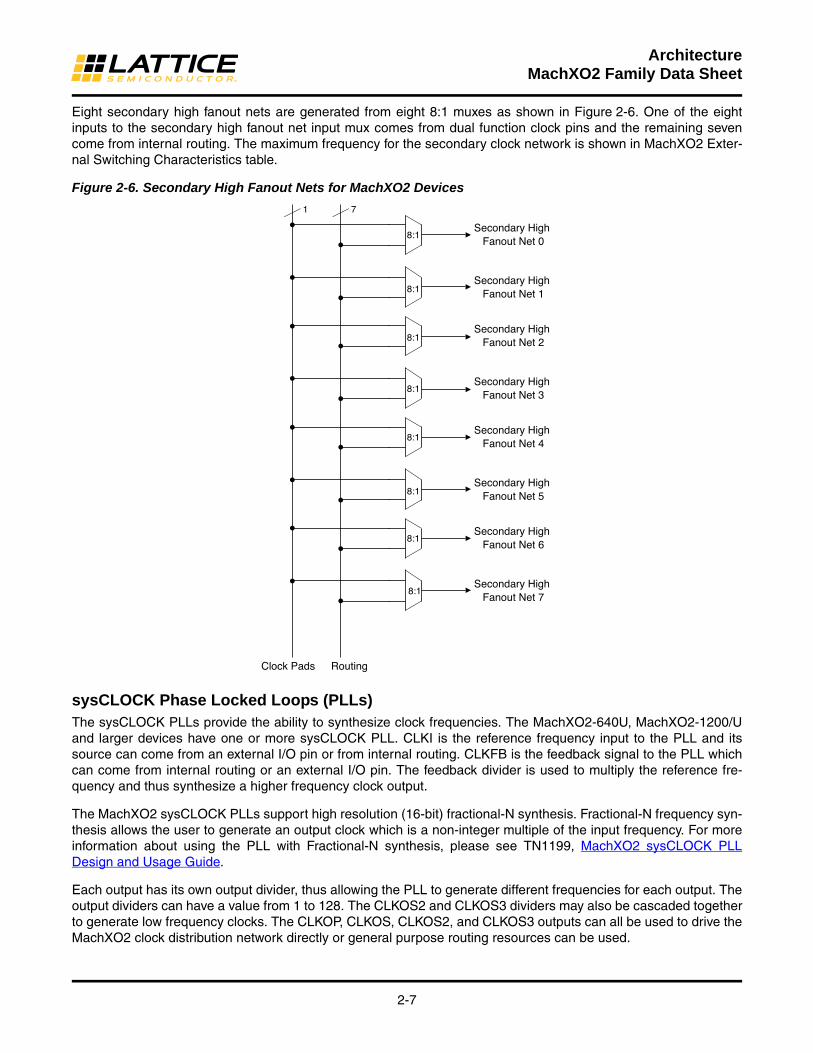
Eight secondary high fanout nets are generated from eight 8:1 muxes as shown in Figure 2-6. One of the eight inputs to the secondary high fanout net input mux comes from dual function clock pins and the remaining seven come from internal routing. The maximum frequency for the secondary clock network is shown in MachXO2 Exter-nal Switching Characteristics table.
Figure 2-6. Secondary High Fanout Nets for MachXO2 Devices
sysCLOCK Phase Locked Loops (PLLs)The sysCLOCK PLLs provide the ability to synthesize clock frequencies. The MachXO2-640U, MachXO2-1200/U and larger devices have one or more sysCLOCK PLL. CLKI is the reference frequency input to the PLL and its source can come from an external I/O pin or from internal routing. CLKFB is the feedback signal to the PLL which can come from internal routing or an external I/O pin. The feedback divider is used to multiply the reference fre-quency and thus synthesize a higher frequency clock output.
The MachXO2 sysCLOCK PLLs support high resolution (16-bit) fractional-N synthesis. Fractional-N frequency syn-thesis allows the user to generate an output clock which is a non-integer multiple of the input frequency. For more information about using the PLL with Fractional-N synthesis, please see TN1199, MachXO2 sysCLOCK PLL Design and Usage Guide.
Each output has its own output divider, thus allowing the PLL to generate different frequencies for each output. The output dividers can have a value from 1 to 128. The CLKOS2 and CLKOS3 dividers may also be cascaded together to generate low frequency clocks. The CLKOP, CLKOS, CLKOS2, and CLKOS3 outputs can all be used to drive the MachXO2 clock distribution network directly or general purpose routing resources can be used.
1 7
8:1
8:1
8:1
8:1
8:1
8:1
8:1
8:1
Clock Pads Routing
Secondary High Fanout Net 0
Secondary High Fanout Net 1
Secondary High Fanout Net 2
Secondary High Fanout Net 3
Secondary High Fanout Net 4
Secondary High Fanout Net 5
Secondary High Fanout Net 6
Secondary High Fanout Net 7
2-8
ArchitectureMachXO2 Family Data Sheet
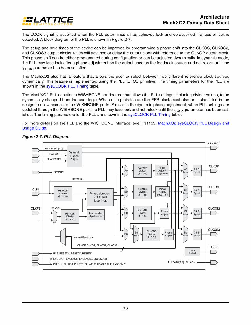
The LOCK signal is asserted when the PLL determines it has achieved lock and de-asserted if a loss of lock is detected. A block diagram of the PLL is shown in Figure 2-7.
The setup and hold times of the device can be improved by programming a phase shift into the CLKOS, CLKOS2, and CLKOS3 output clocks which will advance or delay the output clock with reference to the CLKOP output clock. This phase shift can be either programmed during configuration or can be adjusted dynamically. In dynamic mode, the PLL may lose lock after a phase adjustment on the output used as the feedback source and not relock until the tLOCK parameter has been satisfied.
The MachXO2 also has a feature that allows the user to select between two different reference clock sources dynamically. This feature is implemented using the PLLREFCS primitive. The timing parameters for the PLL are shown in the sysCLOCK PLL Timing table.
The MachXO2 PLL contains a WISHBONE port feature that allows the PLL settings, including divider values, to be dynamically changed from the user logic. When using this feature the EFB block must also be instantiated in the design to allow access to the WISHBONE ports. Similar to the dynamic phase adjustment, when PLL settings are updated through the WISHBONE port the PLL may lose lock and not relock until the tLOCK parameter has been sat-isfied. The timing parameters for the PLL are shown in the sysCLOCK PLL Timing table.
For more details on the PLL and the WISHBONE interface, see TN1199, MachXO2 sysCLOCK PLL Design and Usage Guide.
Figure 2-7. PLL Diagram
CLKOP, CLKOS, CLKOS2, CLKOS3
REFCLK
Internal Feedback
FBKSEL
CLKOP
CLKOS
4
CLKOS2
CLKOS3
REFCLK Divider
M (1 - 40)
LOCK
ENCLKOP, ENCLKOS, ENCLKOS2, ENCLKOS3
RST, RESETM, RESETC, RESETD
CLKFB
CLKI
Dynamic Phase Adjust
PHASESEL[1:0]
PHASEDIR
PHASESTEP
FBKCLK Divider
N (1 - 40)
Fractional-NSynthesizer
Phase detector,VCO, and loop filter.
CLKOS3 Divider
(1 - 128)
CLKOS2 Divider
(1 - 128)
Phase Adjust
Phase Adjust
Phase Adjust/
Edge Trim
CLKOS Divider
(1 - 128)
CLKOP Divider
(1 - 128)
LockDetect
ClkEnSynch
ClkEnSynch
ClkEnSynch
ClkEnSynch
PLLDATO[7:0] , PLLACKPLLCLK, PLLRST, PLLSTB, PLLWE, PLLDATI[7:0], PLLADDR[4:0]
A0
B0
C0
D0D1
Mux
A2Mux
B2Mux
C2Mux
D2Mux
DPHSRC
Phase Adjust/
Edge TrimSTDBY

2-9
ArchitectureMachXO2 Family Data Sheet
Table 2-4 provides signal descriptions of the PLL block.
sysMEM Embedded Block RAM MemoryThe MachXO2-640/U and larger devices contain sysMEM Embedded Block RAMs (EBRs). The EBR consists of a 9-Kbit RAM, with dedicated input and output registers. This memory can be used for a wide variety of purposes including data buffering, PROM for the soft processor and FIFO.
sysMEM Memory BlockThe sysMEM block can implement single port, dual port, pseudo dual port, or FIFO memories. Each block can be used in a variety of depths and widths as shown in Table 2-5.
Table 2-4. PLL Signal Descriptions
Port Name I/O Description
CLKI I Input clock to PLL
CLKFB I Feedback clock
PHASESEL[1:0] I Select which output is affected by Dynamic Phase adjustment ports
PHASEDIR I Dynamic Phase adjustment direction
PHASESTEP I Dynamic Phase step – toggle shifts VCO phase adjust by one step.
CLKOP O Primary PLL output clock (with phase shift adjustment)
CLKOS O Secondary PLL output clock (with phase shift adjust)
CLKOS2 O Secondary PLL output clock2 (with phase shift adjust)
CLKOS3 O Secondary PLL output clock3 (with phase shift adjust)
LOCK O PLL LOCK, asynchronous signal. Active high indicates PLL is locked to input and feed-back signals.
DPHSRC O Dynamic Phase source – ports or WISHBONE is active
STDBY I Standby signal to power down the PLL
RST I PLL reset without resetting the M-divider. Active high reset.
RESETM I PLL reset - includes resetting the M-divider. Active high reset.
RESETC I Reset for CLKOS2 output divider only. Active high reset.
RESETD I Reset for CLKOS3 output divider only. Active high reset.
ENCLKOP I Enable PLL output CLKOP
ENCLKOS I Enable PLL output CLKOS when port is active
ENCLKOS2 I Enable PLL output CLKOS2 when port is active
ENCLKOS3 I Enable PLL output CLKOS3 when port is active
PLLCLK I PLL data bus clock input signal
PLLRST I PLL data bus reset. This resets only the data bus not any register values.
PLLSTB I PLL data bus strobe signal
PLLWE I PLL data bus write enable signal
PLLADDR [4:0] I PLL data bus address
PLLDATI [7:0] I PLL data bus data input
PLLDATO [7:0] O PLL data bus data output
PLLACK O PLL data bus acknowledge signal

2-10
ArchitectureMachXO2 Family Data Sheet
Table 2-5. sysMEM Block Configurations
Bus Size MatchingAll of the multi-port memory modes support different widths on each of the ports. The RAM bits are mapped LSB word 0 to MSB word 0, LSB word 1 to MSB word 1, and so on. Although the word size and number of words for each port varies, this mapping scheme applies to each port.
RAM Initialization and ROM OperationIf desired, the contents of the RAM can be pre-loaded during device configuration. EBR initialization data can be loaded from the UFM. To maximize the number of UFM bits, initialize the EBRs used in your design to an all-zero pattern. Initializing to an all-zero pattern does not use up UFM bits. MachXO2 devices have been designed such that multiple EBRs share the same initialization memory space if they are initialized to the same pattern.
By preloading the RAM block during the chip configuration cycle and disabling the write controls, the sysMEM block can also be utilized as a ROM.
Memory CascadingLarger and deeper blocks of RAM can be created using EBR sysMEM Blocks. Typically, the Lattice design tools cascade memory transparently, based on specific design inputs.
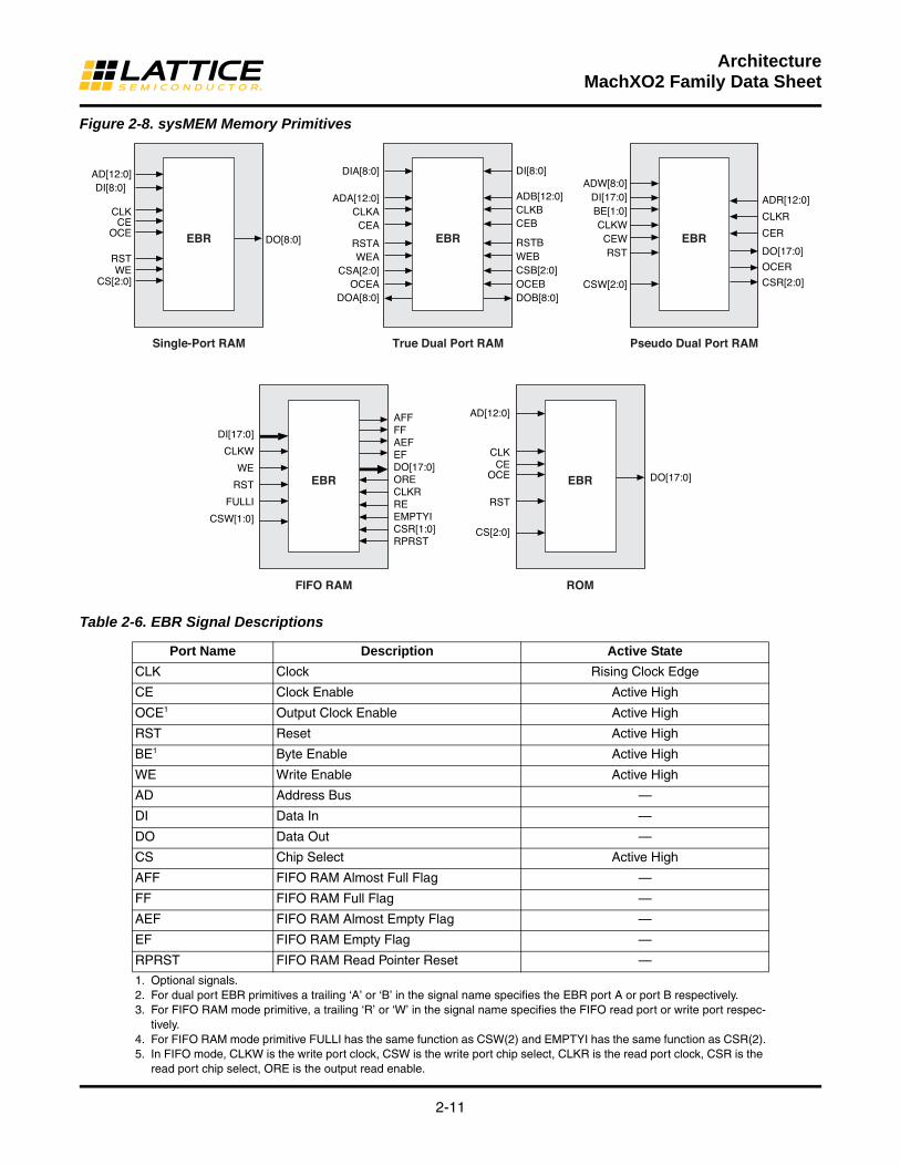
Single, Dual, Pseudo-Dual Port and FIFO ModesFigure 2-8 shows the five basic memory configurations and their input/output names. In all the sysMEM RAM modes, the input data and addresses for the ports are registered at the input of the memory array. The output data of the memory is optionally registered at the memory array output.
Memory Mode Configurations
Single Port
8,192 x 14,096 x 22,048 x 41,024 x 9
True Dual Port
8,192 x 14,096 x 22,048 x 41,024 x 9
Pseudo Dual Port
8,192 x 14,096 x 22,048 x 41,024 x 9512 x 18
FIFO
8,192 x 14,096 x 22,048 x 41,024 x 9512 x 18
2-11
ArchitectureMachXO2 Family Data Sheet
Figure 2-8. sysMEM Memory Primitives
Table 2-6. EBR Signal Descriptions
Port Name Description Active State
CLK Clock Rising Clock Edge
CE Clock Enable Active High
OCE1 Output Clock Enable Active High
RST Reset Active High
BE1 Byte Enable Active High
WE Write Enable Active High
AD Address Bus —
DI Data In —
DO Data Out —
CS Chip Select Active High
AFF FIFO RAM Almost Full Flag —
FF FIFO RAM Full Flag —
AEF FIFO RAM Almost Empty Flag —
EF FIFO RAM Empty Flag —
RPRST FIFO RAM Read Pointer Reset —
1. Optional signals.2. For dual port EBR primitives a trailing ‘A’ or ‘B’ in the signal name specifies the EBR port A or port B respectively.3. For FIFO RAM mode primitive, a trailing ‘R’ or ‘W’ in the signal name specifies the FIFO read port or write port respec-
tively.4. For FIFO RAM mode primitive FULLI has the same function as CSW(2) and EMPTYI has the same function as CSR(2).5. In FIFO mode, CLKW is the write port clock, CSW is the write port chip select, CLKR is the read port clock, CSR is the
read port chip select, ORE is the output read enable.
DI[17:0]
CLKW
WE
FIFO RAM
DO[17:0]
RST
FULLI
AFFFFAEFEF
CLKRRE
CSR[1:0]
ORE
RPRST
CSW[1:0] EMPTYI
ROM
DO[17:0]
AD[12:0]
CLKCE
RST
CS[2:0]
OCEEBR EBR
AD[12:0]DI[8:0]
DO[8:0]
CLKCE
RSTWE
CS[2:0]
OCE
Single-Port RAM
ADA[12:0]
DIA[8:0]
CLKACEA
RSTAWEA
CSA[2:0]
DOA[8:0]OCEA
ADB[12:0]
DI[8:0]
CLKBCEB
RSTBWEBCSB[2:0]
DOB[8:0]OCEB
True Dual Port RAM
ADW[8:0]DI[17:0]
CLKWCEWRST
CSW[2:0]
ADR[12:0]
CLKR
CER
DO[17:0]
CSR[2:0]
OCER
BE[1:0]
Pseudo Dual Port RAM
EBREBREBR
2-12
ArchitectureMachXO2 Family Data Sheet
The EBR memory supports three forms of write behavior for single or dual port operation:
1. Normal – Data on the output appears only during the read cycle. During a write cycle, the data (at the current address) does not appear on the output. This mode is supported for all data widths.
2. Write Through – A copy of the input data appears at the output of the same port. This mode is supported for all data widths.
3. Read-Before-Write – When new data is being written, the old contents of the address appears at the output.
FIFO ConfigurationThe FIFO has a write port with data-in, CEW, WE and CLKW signals. There is a separate read port with data-out, RCE, RE and CLKR signals. The FIFO internally generates Almost Full, Full, Almost Empty and Empty Flags. The Full and Almost Full flags are registered with CLKW. The Empty and Almost Empty flags are registered with CLKR. Table 2-7 shows the range of programming values for these flags.
Table 2-7. Programmable FIFO Flag Ranges
The FIFO state machine supports two types of reset signals: RST and RPRST. The RST signal is a global reset that clears the contents of the FIFO by resetting the read/write pointer and puts the FIFO flags in their initial reset state. The RPRST signal is used to reset the read pointer. The purpose of this reset is to retransmit the data that is in the FIFO. In these applications it is important to keep careful track of when a packet is written into or read from the FIFO.
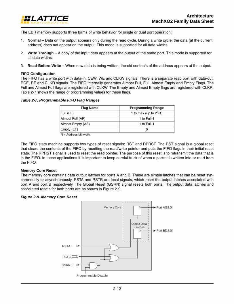
Memory Core ResetThe memory core contains data output latches for ports A and B. These are simple latches that can be reset syn-chronously or asynchronously. RSTA and RSTB are local signals, which reset the output latches associated with port A and port B respectively. The Global Reset (GSRN) signal resets both ports. The output data latches and associated resets for both ports are as shown in Figure 2-9.
Figure 2-9. Memory Core Reset
Flag Name Programming Range
Full (FF) 1 to max (up to 2N-1)
Almost Full (AF) 1 to Full-1
Almost Empty (AE) 1 to Full-1
Empty (EF) 0
N = Address bit width.
QSETD
Output Data Latches
Memory Core Port A[18:0]
QSETD Port B[18:0]
RSTB
GSRN
Programmable Disable
RSTA
2-13
ArchitectureMachXO2 Family Data Sheet
For further information on the sysMEM EBR block, please refer to TN1201, Memory Usage Guide for MachXO2 Devices.
EBR Asynchronous ResetEBR asynchronous reset or GSR (if used) can only be applied if all clock enables are low for a clock cycle before the reset is applied and released a clock cycle after the reset is released, as shown in Figure 2-10. The GSR input to the EBR is always asynchronous.
Figure 2-10. EBR Asynchronous Reset (Including GSR) Timing Diagram
If all clock enables remain enabled, the EBR asynchronous reset or GSR may only be applied and released after the EBR read and write clock inputs are in a steady state condition for a minimum of 1/fMAX (EBR clock). The reset release must adhere to the EBR synchronous reset setup time before the next active read or write clock edge.
If an EBR is pre-loaded during configuration, the GSR input must be disabled or the release of the GSR during device wake up must occur before the release of the device I/Os becoming active.
These instructions apply to all EBR RAM, ROM and FIFO implementations. For the EBR FIFO mode, the GSR sig-nal is always enabled and the WE and RE signals act like the clock enable signals in Figure 2-10. The reset timing rules apply to the RPReset input versus the RE input and the RST input versus the WE and RE inputs. Both RST and RPReset are always asynchronous EBR inputs. For more details refer to TN1201, Memory Usage Guide for MachXO2 Devices.
Note that there are no reset restrictions if the EBR synchronous reset is used and the EBR GSR input is disabled.
Programmable I/O Cells (PIC)The programmable logic associated with an I/O is called a PIO. The individual PIO are connected to their respec-tive sysIO buffers and pads. On the MachXO2 devices, the PIO cells are assembled into groups of four PIO cells called a Programmable I/O Cell or PIC. The PICs are placed on all four sides of the device.
On all the MachXO2 devices, two adjacent PIOs can be combined to provide a complementary output driver pair.
The MachXO2-640U, MachXO2-1200/U and higher density devices contain enhanced I/O capability. All PIO pairs on these larger devices can implement differential receivers. Half of the PIO pairs on the top edge of these devices can be configured as true LVDS transmit pairs. The PIO pairs on the bottom edge of these higher density devices have on-chip differential termination and also provide PCI support.
Reset
Clock
Clock Enable

2-14
ArchitectureMachXO2 Family Data Sheet
Figure 2-11. Group of Four Programmable I/O Cells
1 PIC
PIO A
Output Register Block
& Tristate Register Block
Pin A
Input Register Block
PIO B
Output Register Block
& Tristate Register Block
Pin B
Input Register Block
PIO C
Output Register Block
& Tristate Register Block
Pin C
Input Register Block
Notes:1. Input gearbox is available only in PIC on the bottom edge of MachXO2-640U, MachXO2-1200/U and larger devices.2. Output gearbox is available only in PIC on the top edge of MachXO2-640U, MachXO2-1200/U and larger devices.
PIO D
Output Register Block
& Tristate Register Block
Pin D
Input Register Block
Core Logic/Routing
InputGearbox
OutputGearbox

2-15
ArchitectureMachXO2 Family Data Sheet
PIO The PIO contains three blocks: an input register block, output register block and tri-state register block. These blocks contain registers for operating in a variety of modes along with the necessary clock and selection logic.
Table 2-8. PIO Signal List
Input Register Block The input register blocks for the PIOs on all edges contain delay elements and registers that can be used to condi-tion high-speed interface signals before they are passed to the device core. In addition to this functionality, the input register blocks for the PIOs on the right edge include built-in logic to interface to DDR memory.
Figure 2-12 shows the input register block for the PIOs located on the left, top and bottom edges. Figure 2-13 shows the input register block for the PIOs on the right edge.
Left, Top, Bottom EdgesInput signals are fed from the sysIO buffer to the input register block (as signal D). If desired, the input signal can bypass the register and delay elements and be used directly as a combinatorial signal (INDD), and a clock (INCK). If an input delay is desired, users can select a fixed delay. I/Os on the bottom edge also have a dynamic delay, DEL[4:0]. The delay, if selected, reduces input register hold time requirements when using a global clock. The input block allows two modes of operation. In single data rate (SDR) the data is registered with the system clock (SCLK) by one of the registers in the single data rate sync register block. In Generic DDR mode, two registers are used to sample the data on the positive and negative edges of the system clock (SCLK) signal, creating two data streams.
Pin Name I/O Type Description
CE Input Clock Enable
D Input Pin input from sysIO buffer.
INDD Output Register bypassed input.
INCK Output Clock input
Q0 Output DDR positive edge input
Q1 Output Registered input/DDR negative edge input
D0 Input Output signal from the core (SDR and DDR)
D1 Input Output signal from the core (DDR)
TD Input Tri-state signal from the core
Q Output Data output signals to sysIO Buffer
TQ Output Tri-state output signals to sysIO Buffer
DQSR901 Input DQS shift 90-degree read clock
DQSW901 Input DQS shift 90-degree write clock
DDRCLKPOL1 Input DDR input register polarity control signal from DQS
SCLK Input System clock for input and output/tri-state blocks.
RST Input Local set reset signal
1. Available in PIO on right edge only.

2-16
ArchitectureMachXO2 Family Data Sheet
Figure 2-12. MachXO2 Input Register Block Diagram (PIO on Left, Top and Bottom Edges)
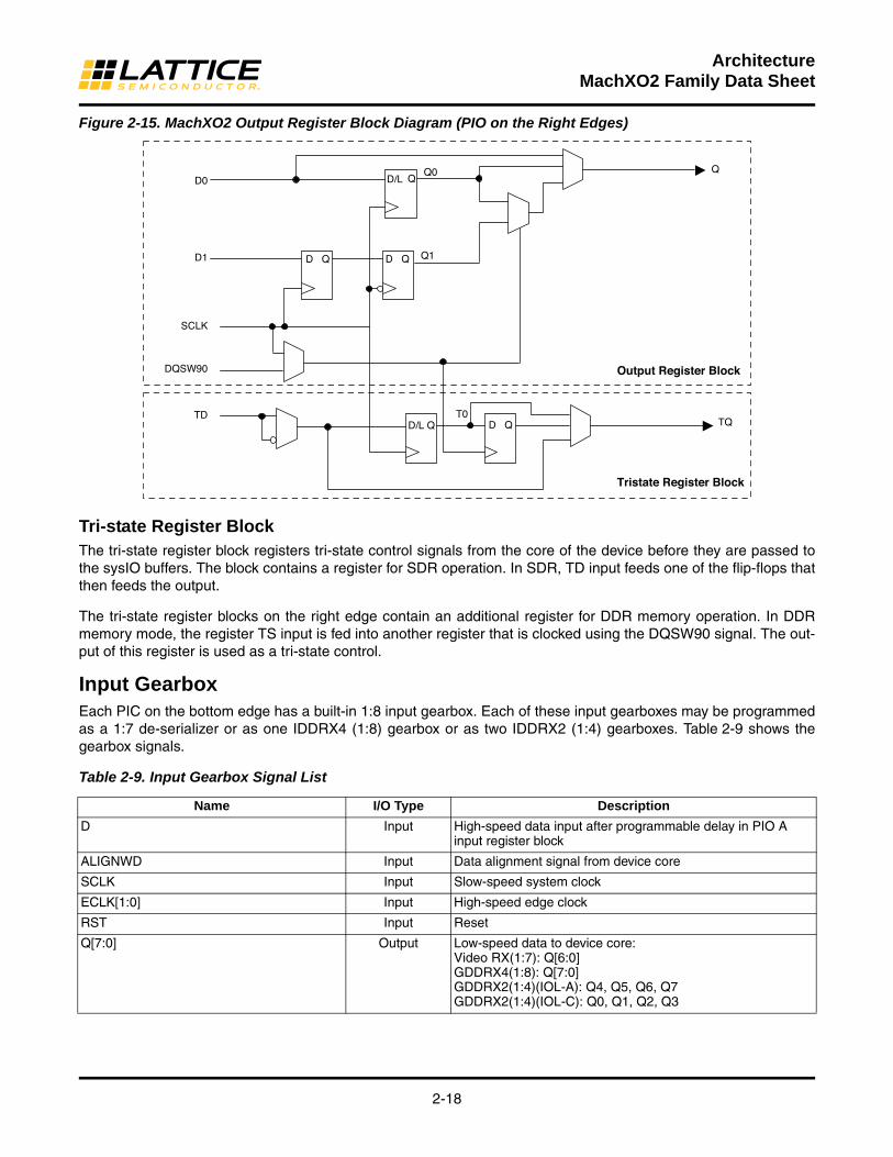
Right EdgeThe input register block on the right edge is a superset of the same block on the top, bottom, and left edges. In addition to the modes described above, the input register block on the right edge also supports DDR memory mode.
In DDR memory mode, two registers are used to sample the data on the positive and negative edges of the modi-fied DQS (DQSR90) in the DDR Memory mode creating two data streams. Before entering the core, these two data streams are synchronized to the system clock to generate two data streams.
The signal DDRCLKPOL controls the polarity of the clock used in the synchronization registers. It ensures ade-quate timing when data is transferred to the system clock domain from the DQS domain. The DQSR90 and DDRCLKPOL signals are generated in the DQS read-write block.
Figure 2-13. MachXO2 Input Register Block Diagram (PIO on Right Edge)
Output Register Block The output register block registers signals from the core of the device before they are passed to the sysIO buffers.
Left, Top, Bottom EdgesIn SDR mode, D0 feeds one of the flip-flops that then feeds the output. The flip-flop can be configured as a D-type register or latch.
SCLK
INCK
Q1
Q0
INDD
D
Q0
Q1
D Q
ProgrammableDelay Cell D/L Q D Q
D Q
Q1
Q0
INDD
D
DQSR90
Q0
Q1
SCLK
S0
S1
DDRCLKPOL
ProgrammableDelay Cell D/L Q
INCK
D Q
D Q D Q
D Q D Q D Q
D Q
2-17
ArchitectureMachXO2 Family Data Sheet
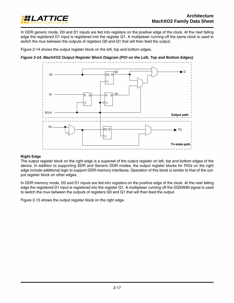
In DDR generic mode, D0 and D1 inputs are fed into registers on the positive edge of the clock. At the next falling edge the registered D1 input is registered into the register Q1. A multiplexer running off the same clock is used to switch the mux between the outputs of registers Q0 and Q1 that will then feed the output.
Figure 2-14 shows the output register block on the left, top and bottom edges.
Figure 2-14. MachXO2 Output Register Block Diagram (PIO on the Left, Top and Bottom Edges)
Right EdgeThe output register block on the right edge is a superset of the output register on left, top and bottom edges of the device. In addition to supporting SDR and Generic DDR modes, the output register blocks for PIOs on the right edge include additional logic to support DDR-memory interfaces. Operation of this block is similar to that of the out-put register block on other edges.
In DDR memory mode, D0 and D1 inputs are fed into registers on the positive edge of the clock. At the next falling edge the registered D1 input is registered into the register Q1. A multiplexer running off the DQSW90 signal is used to switch the mux between the outputs of registers Q0 and Q1 that will then feed the output.
Figure 2-15 shows the output register block on the right edge.
Output path
TQ D/L Q TD
Tri-state path
Q
D1 D Q D Q Q1
D/L QQ0
D0
SCLK
2-18
ArchitectureMachXO2 Family Data Sheet
Figure 2-15. MachXO2 Output Register Block Diagram (PIO on the Right Edges)
Tri-state Register Block The tri-state register block registers tri-state control signals from the core of the device before they are passed to the sysIO buffers. The block contains a register for SDR operation. In SDR, TD input feeds one of the flip-flops that then feeds the output.
The tri-state register blocks on the right edge contain an additional register for DDR memory operation. In DDR memory mode, the register TS input is fed into another register that is clocked using the DQSW90 signal. The out-put of this register is used as a tri-state control.
Input Gearbox Each PIC on the bottom edge has a built-in 1:8 input gearbox. Each of these input gearboxes may be programmed as a 1:7 de-serializer or as one IDDRX4 (1:8) gearbox or as two IDDRX2 (1:4) gearboxes. Table 2-9 shows the gearbox signals.
Table 2-9. Input Gearbox Signal List
Name I/O Type Description
D Input High-speed data input after programmable delay in PIO A input register block
ALIGNWD Input Data alignment signal from device core
SCLK Input Slow-speed system clock
ECLK[1:0] Input High-speed edge clock
RST Input Reset
Q[7:0] Output Low-speed data to device core:Video RX(1:7): Q[6:0]GDDRX4(1:8): Q[7:0]GDDRX2(1:4)(IOL-A): Q4, Q5, Q6, Q7GDDRX2(1:4)(IOL-C): Q0, Q1, Q2, Q3
D Q D1 D Q Q1
D/L QQ0
D0
DQSW90
Q
SCLK
D Q TQ D/L Q T0 TD
Output Register Block
Tristate Register Block

2-19
ArchitectureMachXO2 Family Data Sheet
These gearboxes have three stage pipeline registers. The first stage registers sample the high-speed input data by the high-speed edge clock on its rising and falling edges. The second stage registers perform data alignment based on the control signals UPDATE and SEL0 from the control block. The third stage pipeline registers pass the data to the device core synchronized to the low-speed system clock. Figure 2-16 shows a block diagram of the input gearbox.
Figure 2-16. Input Gearbox
D Q
D
ECLK0/1 SCLK
Q21
Q0_
S2
S0 D Q
D QT2
T0 Q0
Q2
D Q
D QCE
D QCE
D QQ65
Q43
S6
S4 D Q
D QT6
T4 D Q
cdn
D QCE
D Q
cdn
CE
D QQ54
Q_6
S3
S5 D
DT3
T5
Q6
D Q
D QCE
D QCE
D QQ10
Q32
S1 D
T1
D Q
D QCE
Q65
Q65
Q43
Q43
Q21
Q10
Q21
Q32
Q54
Q_6
Q54
Q32
SEL0
Q4
Q5
Q1
Q3
S7 D Q
T7 D QCE
Q7
UPDATE
Q_6
2-20
ArchitectureMachXO2 Family Data Sheet
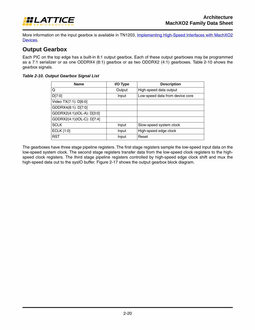
More information on the input gearbox is available in TN1203, Implementing High-Speed Interfaces with MachXO2 Devices.
Output Gearbox Each PIC on the top edge has a built-in 8:1 output gearbox. Each of these output gearboxes may be programmed as a 7:1 serializer or as one ODDRX4 (8:1) gearbox or as two ODDRX2 (4:1) gearboxes. Table 2-10 shows the gearbox signals.
Table 2-10. Output Gearbox Signal List
The gearboxes have three stage pipeline registers. The first stage registers sample the low-speed input data on the low-speed system clock. The second stage registers transfer data from the low-speed clock registers to the high-speed clock registers. The third stage pipeline registers controlled by high-speed edge clock shift and mux the high-speed data out to the sysIO buffer. Figure 2-17 shows the output gearbox block diagram.
Name I/O Type Description
Q Output High-speed data output
D[7:0] Input Low-speed data from device core
Video TX(7:1): D[6:0]
GDDRX4(8:1): D[7:0]
GDDRX2(4:1)(IOL-A): D[3:0]
GDDRX2(4:1)(IOL-C): D[7:4]
SCLK Input Slow-speed system clock
ECLK [1:0] Input High-speed edge clock
RST Input Reset

2-21
ArchitectureMachXO2 Family Data Sheet
Figure 2-17. Output Gearbox
More information on the output gearbox is available in TN1203, Implementing High-Speed Interfaces with MachXO2 Devices.
DDR Memory Support Certain PICs on the right edge of MachXO2-640U, MachXO2-1200/U and larger devices, have additional circuitry to allow the implementation of DDR memory interfaces. There are two groups of 14 or 12 PIOs each on the right edge with additional circuitry to implement DDR memory interfaces. This capability allows the implementation of up to 16-bit wide memory interfaces. One PIO from each group contains a control element, the DQS Read/Write
D4
D0
D3
D1 S1T1
S0
QC
ODDRx2_A
ODDRx2_C
ODDRx2_C
ECLK0/1
Q45
Q67
S4
S6D Q
D QT4
T6D6 D Q
D QCE
D QCE
01
01
Q01
Q23
S0
S2
T0
T2
Q32
Q10
S5
S3
D Q T5
T3
CE01
D QQ76
Q54
S7D Q T7
D Q
D Q
D Q
CE01
S2
S4
GND
S7
S6
S5
S3D2
D7
D5
SCLK
01
01
01
1
01
Q34
Q56
Q67
GND
Q45
S1
Q12
SEL /0
UPDATE
Q23
Q/QA
D Q
D Q
D Q
D Q
D QD Q
D Q
D Q
D Q
D Q
D Q
0
10
10
10
10
10
CE
CE
D QCE
D QCE
01
01
CDN
2-22
ArchitectureMachXO2 Family Data Sheet
Block, to facilitate the generation of clock and control signals (DQSR90, DQSW90, DDRCLKPOL and DATAVALID). These clock and control signals are distributed to the other PIO in the group through dedicated low skew routing.
DQS Read Write Block Source synchronous interfaces generally require the input clock to be adjusted in order to correctly capture data at the input register. For most interfaces a PLL is used for this adjustment. However, in DDR memories the clock (referred to as DQS) is not free-running so this approach cannot be used. The DQS Read Write block provides the required clock alignment for DDR memory interfaces. DQSR90 and DQSW90 signals are generated by the DQS Read Write block from the DQS input.
In a typical DDR memory interface design, the phase relationship between the incoming delayed DQS strobe and the internal system clock (during the read cycle) is unknown. The MachXO2 family contains dedicated circuits to transfer data between these domains. To prevent set-up and hold violations, at the domain transfer between DQS (delayed) and the system clock, a clock polarity selector is used. This circuit changes the edge on which the data is registered in the synchronizing registers in the input register block. This requires evaluation at the start of each read cycle for the correct clock polarity. Prior to the read operation in DDR memories, DQS is in tri-state (pulled by termination). The DDR memory device drives DQS low at the start of the preamble state. A dedicated circuit in the DQS Read Write block detects the first DQS rising edge after the preamble state and generates the DDRCLKPOL signal. This signal is used to control the polarity of the clock to the synchronizing registers.
The temperature, voltage and process variations of the DQS delay block are compensated by a set of calibration signals (6-bit bus) from a DLL on the right edge of the device. The DLL loop is compensated for temperature, volt-age and process variations by the system clock and feedback loop.
sysIO BufferEach I/O is associated with a flexible buffer referred to as a sysIO buffer. These buffers are arranged around the periphery of the device in groups referred to as banks. The sysIO buffers allow users to implement a wide variety of standards that are found in today’s systems including LVCMOS, TTL, PCI, SSTL, HSTL, LVDS, BLVDS, MLVDS and LVPECL.
Each bank is capable of supporting multiple I/O standards. In the MachXO2 devices, single-ended output buffers, ratioed input buffers (LVTTL, LVCMOS and PCI), differential (LVDS) and referenced input buffers (SSTL and HSTL) are powered using I/O supply voltage (VCCIO). Each sysIO bank has its own VCCIO. In addition, each bank has a voltage reference, VREF, which allows the use of referenced input buffers independent of the bank VCCIO.
MachXO2-256 and MachXO2-640 devices contain single-ended ratioed input buffers and single-ended output buf-fers with complementary outputs on all the I/O banks. Note that the single-ended input buffers on these devices do not contain PCI clamps. In addition to the single-ended I/O buffers these two devices also have differential and ref-erenced input buffers on all I/Os. The I/Os are arranged in pairs, the two pads in the pair are described as “T” and “C”, where the true pad is associated with the positive side of the differential input buffer and the comp (comple-mentary) pad is associated with the negative side of the differential input buffer.
MachXO2-640U, MachXO2-1200/U, MachXO2-2000/U, MachXO2-4000 and MachXO2-7000 devices contain three types of sysIO buffer pairs.
1. Left and Right sysIO Buffer PairsThe sysIO buffer pairs in the left and right banks of the device consist of two single-ended output drivers and two single-ended input buffers (for ratioed inputs such as LVCMOS and LVTTL). The I/O pairs on the left and right of the devices also have differential and referenced input buffers.
2. Bottom sysIO Buffer PairsThe sysIO buffer pairs in the bottom bank of the device consist of two single-ended output drivers and two sin-gle-ended input buffers (for ratioed inputs such as LVCMOS and LVTTL). The I/O pairs on the bottom also have differential and referenced input buffers. Only the I/Os on the bottom banks have programmable PCI clamps

2-23
ArchitectureMachXO2 Family Data Sheet
and differential input termination. The PCI clamp is enabled after VCC and VCCIO are at valid operating levels and the device has been configured.
3. Top sysIO Buffer PairsThe sysIO buffer pairs in the top bank of the device consist of two single-ended output drivers and two single-ended input buffers (for ratioed inputs such as LVCMOS and LVTTL). The I/O pairs on the top also have differ-ential and referenced I/O buffers. Half of the sysIO buffer pairs on the top edge have true differential outputs. The sysIO buffer pair comprising of the A and B PIOs in every PIC on the top edge have a differential output driver. The referenced input buffer can also be configured as a differential input buffer.
Typical I/O Behavior During Power-upThe internal power-on-reset (POR) signal is deactivated when VCC and VCCIO0 have reached VPORUP level defined in the Power-On-Reset Voltage table in the DC and Switching Characteristics section of this data sheet. After the POR signal is deactivated, the FPGA core logic becomes active. It is the user’s responsibility to ensure that all VCCIO banks are active with valid input logic levels to properly control the output logic states of all the I/O banks that are critical to the application. The default configuration of the I/O pins in a blank device is tri-state with a weak pull-down to GND (some pins such as PROGRAMN and the JTAG pins have weak pull-up to VCCIO as the default func-tionality). The I/O pins will maintain the blank configuration until VCC and VCCIO (for I/O banks containing configura-tion I/Os) have reached VPORUP levels at which time the I/Os will take on the user-configured settings only after a proper download/configuration.
There are various ways a user can ensure that there are no spurious signals on critical outputs as the device pow-ers up. These are discussed in more detail in TN1202, MachXO2 sysIO Usage Guide.
Supported StandardsThe MachXO2 sysIO buffer supports both single-ended and differential standards. Single-ended standards can be further subdivided into LVCMOS, LVTTL, and PCI. The buffer supports the LVTTL, PCI, LVCMOS 1.2, 1.5, 1.8, 2.5, and 3.3V standards. In the LVCMOS and LVTTL modes, the buffer has individually configurable options for drive strength, bus maintenance (weak pull-up, weak pull-down, bus-keeper latch or none) and open drain. BLVDS, MLVDS and LVPECL output emulation is supported on all devices. The MachXO2-640U, MachXO2-1200/U and higher devices support on-chip LVDS output buffers on approximately 50% of the I/Os on the top bank. Differential receivers for LVDS, BLVDS, MLVDS and LVPECL are supported on all banks of MachXO2 devices. PCI support is provided in the bottom bank of theMachXO2-640U, MachXO2-1200/U and higher density devices. Table 2-11 sum-marizes the I/O characteristics of the MachXO2 PLDs.
Tables 2-11 and 2-12 show the I/O standards (together with their supply and reference voltages) supported by the MachXO2 devices. For further information on utilizing the sysIO buffer to support a variety of standards please see TN1202, MachXO2 sysIO Usage Guide.
Table 2-11. I/O Support Device by Device
MachXO2-256, MachXO2-640
MachXO2-640U,MachXO2-1200
MachXO2-1200UMachXO2-2000/U, MachXO2-4000, MachXO2-7000
Number of I/O Banks 4 4 6
Type of Input Buffers
Single-ended (all I/O banks)
Differential Receivers (all I/O banks)
Single-ended (all I/O banks)
Differential Receivers (all I/O banks)
Differential input termination (bottom side)
Single-ended (all I/O banks)
Differential Receivers (all I/O banks)
Differential input termination (bottom side)

2-24
ArchitectureMachXO2 Family Data Sheet
Table 2-12. Supported Input Standards
Types of Output BuffersSingle-ended buffers with complementary outputs (all I/O banks)
Single-ended buffers with complementary outputs (all I/O banks)
Differential buffers with true LVDS outputs (50% on top side)
Single-ended buffers with complementary outputs (all I/O banks)
Differential buffers with true LVDS outputs (50% on top side)
Differential Output Emulation Capability All I/O banks All I/O banks All I/O banks
PCI Clamp Support No Clamp on bottom side only Clamp on bottom side only
VCCIO (Typ.)
Input Standard 3.3V 2.5V 1.8V 1.5 1.2V
Single-Ended Interfaces
LVTTL 2 2 2
LVCMOS33 2 2 2
LVCMOS25 2 2 2
LVCMOS18 2 2 2
LVCMOS15 2 2 2 2
LVCMOS12 2 2 2 2
PCI1
SSTL18 (Class I, Class II)
SSTL25 (Class I, Class II)
HSTL18 (Class I, Class II)
Differential Interfaces
LVDS
BLVDS, MVDS, LVPECL, RSDS
Differential SSTL18 Class I, II
Differential SSTL25 Class I, II
Differential HSTL18 Class I, II
1. Bottom banks of MachXO2-640U, MachXO2-1200/U and higher density devices only.2. Reduced functionality. Refer to TN1202, MachXO2 sysIO Usage Guide for more detail.
MachXO2-256, MachXO2-640
MachXO2-640U,MachXO2-1200
MachXO2-1200UMachXO2-2000/U, MachXO2-4000, MachXO2-7000
2-25
ArchitectureMachXO2 Family Data Sheet
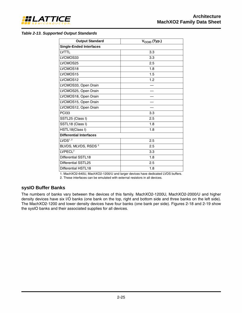
Table 2-13. Supported Output Standards
sysIO Buffer BanksThe numbers of banks vary between the devices of this family. MachXO2-1200U, MachXO2-2000/U and higher density devices have six I/O banks (one bank on the top, right and bottom side and three banks on the left side). The MachXO2-1200 and lower density devices have four banks (one bank per side). Figures 2-18 and 2-19 show the sysIO banks and their associated supplies for all devices.
Output Standard VCCIO (Typ.)
Single-Ended Interfaces
LVTTL 3.3
LVCMOS33 3.3
LVCMOS25 2.5
LVCMOS18 1.8
LVCMOS15 1.5
LVCMOS12 1.2
LVCMOS33, Open Drain —
LVCMOS25, Open Drain —
LVCMOS18, Open Drain —
LVCMOS15, Open Drain —
LVCMOS12, Open Drain —
PCI33 3.3
SSTL25 (Class I) 2.5
SSTL18 (Class I) 1.8
HSTL18(Class I) 1.8
Differential Interfaces
LVDS1, 2 2.5
BLVDS, MLVDS, RSDS 2 2.5
LVPECL2 3.3
Differential SSTL18 1.8
Differential SSTL25 2.5
Differential HSTL18 1.8
1. MachXO2-640U, MachXO2-1200/U and larger devices have dedicated LVDS buffers.2. These interfaces can be emulated with external resistors in all devices.

2-26
ArchitectureMachXO2 Family Data Sheet
Figure 2-18. MachXO2-1200U, MachXO2-2000/U, MachXO2-4000 and MachXO2-7000 Banks
Figure 2-19. MachXO2-256, MachXO2-640/U and MachXO2-1200 Banks
Bank 0
Bank 1
Bank 2Ban
k 3
Ban
k 4
Ban
k 5
VCCIO0
VCCIO2GND
GND
VCCIO1
GND
GND
GND
GND
VCCIO5
VCCIO4
VCCIO3
Bank 0
Bank 1
Bank 2
Ban
k 3
VCCIO0
VCCIO2GND
GND
VCCIO1
GND
VCCIO3
GND
2-27
ArchitectureMachXO2 Family Data Sheet
Hot SocketingThe MachXO2 devices have been carefully designed to ensure predictable behavior during power-up and power-down. Leakage into I/O pins is controlled to within specified limits. This allows for easy integration with the rest of the system. These capabilities make the MachXO2 ideal for many multiple power supply and hot-swap applica-tions.
On-chip OscillatorEvery MachXO2 device has an internal CMOS oscillator. The oscillator output can be routed as a clock to the clock tree or as a reference clock to the sysCLOCK PLL using general routing resources. The oscillator frequency can be divided by internal logic. There is a dedicated programming bit and a user input to enable/disable the oscillator. The oscillator frequency ranges from 2.08 MHz to 133 MHz. The software default value of the Master Clock (MCLK) is nominally 2.08 MHz. When a different MCLK is selected during the design process, the following sequence takes place:
1. Device powers up with a nominal MCLK frequency of 2.08 MHz.
2. During configuration, users select a different master clock frequency.
3. The MCLK frequency changes to the selected frequency once the clock configuration bits are received.
4. If the user does not select a master clock frequency, then the configuration bitstream defaults to the MCLK fre-quency of 2.08 MHz.
Table 2-14 lists all the available MCLK frequencies.
Table 2-14. Available MCLK Frequencies
Embedded Hardened IP Functions and User Flash MemoryAll MachXO2 devices provide embedded hardened functions such as SPI, I2C and Timer/Counter. MachXO2-640/U and higher density devices also provide User Flash Memory (UFM). These embedded blocks interface through the WISHBONE interface with routing as shown in Figure 2-20.
MCLK (MHz, Nominal) MCLK (MHz, Nominal) MCLK (MHz, Nominal)
2.08 (default) 9.17 33.25
2.46 10.23 38
3.17 13.3 44.33
4.29 14.78 53.2
5.54 20.46 66.5
7 26.6 88.67
8.31 29.56 133

2-28
ArchitectureMachXO2 Family Data Sheet
Figure 2-20. Embedded Function Block Interface
Hardened I2C IP CoreEvery MachXO2 device contains two I2C IP cores. These are the primary and secondary I2C IP cores. Either of the two cores can be configured either as an I2C master or as an I2C slave. The only difference between the two IP cores is that the primary core has pre-assigned I/O pins whereas users can assign I/O pins for the secondary core.
When the IP core is configured as a master it will be able to control other devices on the I2C bus through the inter-face. When the core is configured as the slave, the device will be able to provide I/O expansion to an I2C Master. The I2C cores support the following functionality:
• Master and Slave operation
• 7-bit and 10-bit addressing
• Multi-master arbitration support
• Clock stretching
• Up to 400 KHz data transfer speed
• General call support
• Interface to custom logic through 8-bit WISHBONE interface
Embedded Function Block (EFB)
CoreLogic/
RoutingEFB
WISHBONE Interface
I2C (Primary)
I2C (Secondary)
SPI
Timer/Counter
PLL0 PLL1
ConfigurationLogic
UFM
I/Os for I2C (Primary)
I/Os for SPI
I/Os for I2C (Secondary)
Indicates connectionthrough core logic/routing.
PowerControl

2-29
ArchitectureMachXO2 Family Data Sheet
Figure 2-21. I2C Core Block Diagram
Table 2-15 describes the signals interfacing with the I2C cores.
Table 2-15. I2C Core Signal Description
Hardened SPI IP CoreEvery MachXO2 device has a hard SPI IP core that can be configured as a SPI master or slave. When the IP core is configured as a master it will be able to control other SPI enabled chips connected to the SPI bus. When the core is configured as the slave, the device will be able to interface to an external SPI master. The SPI IP core on MachXO2 devices supports the following functions:
• Configurable Master and Slave modes
• Full-Duplex data transfer
• Mode fault error flag with CPU interrupt capability
• Double-buffered data register
• Serial clock with programmable polarity and phase
• LSB First or MSB First Data Transfer
• Interface to custom logic through 8-bit WISHBONE interface
Signal Name I/O Description
i2c_scl Bi-directional
Bi-directional clock line of the I2C core. The signal is an output if the I2C core is in master mode. The signal is an input if the I2C core is in slave mode. MUST be routed directly to the pre-assigned I/O of the chip. Refer to the Pinout Information section of this document for detailed pad and pin locations of I2C ports in each MachXO2 device.
i2c_sda Bi-directional
Bi-directional data line of the I2C core. The signal is an output when data is transmitted from the I2C core. The signal is an input when data is received into the I2C core. MUST be routed directly to the pre-assigned I/O of the chip. Refer to the Pinout Information section of this document for detailed pad and pin locations of I2C ports in each MachXO2 device.
i2c_irqo Output
Interrupt request output signal of the I2C core. The intended usage of this signal is for it to be connected to the WISHBONE master controller (i.e. a microcontroller or state machine) and request an interrupt when a specific condition is met. These conditions are described with the I2C register definitions.
cfg_wake OutputWake-up signal – To be connected only to the power module of the MachXO2 device. The signal is enabled only if the “Wakeup Enable” feature has been set within the EFB GUI, I2C Tab.
cfg_stdby OutputStand-by signal – To be connected only to the power module of the MachXO2 device. The signal is enabled only if the “Wakeup Enable” feature has been set within the EFB GUI, I2C Tab.
EFB
SCL
SDA
ConfigurationLogic
CoreLogic/
Routing
PowerControl
I2CRegisters
EFBWISHBONE
Interface
ControlLogic
I2C Function

2-30
ArchitectureMachXO2 Family Data Sheet
There are some limitations on the use of the hardened user SPI. These are defined in the following technical notes:
• TN1087, Minimizing System Interruption During Configuration Using TransFR Technology (Appendix B)
• TN1205, Using User Flash Memory and Hardened Control Functions in MachXO2 Devices
Figure 2-22. SPI Core Block Diagram
Table 2-16 describes the signals interfacing with the I2C cores.
Table 2-16. SPI Core Signal Description
Hardened Timer/CounterMachXO2 devices provide a hard Timer/Counter IP core. This Timer/Counter is a general purpose, bi-directional, 16-bit timer/counter module with independent output compare units and PWM support. The Timer/Counter sup-ports the following functions:
Signal Name I/O Master/Slave Description
spi_csn[0] O Master SPI master chip-select output
spi_csn[1..7] O Master Additional SPI chip-select outputs (total up to eight slaves)
spi_scsn I Slave SPI slave chip-select input
spi_irq O Master/Slave Interrupt request
spi_clk I/O Master/Slave SPI clock. Output in master mode. Input in slave mode.
spi_miso I/O Master/Slave SPI data. Input in master mode. Output in slave mode.
spi_mosi I/O Master/Slave SPI data. Output in master mode. Input in slave mode.
ufm_sn I Slave Configuration Slave Chip Select (active low), dedicated for selecting theUser Flash Memory (UFM).
cfg_stdby O Master/SlaveStand-by signal – To be connected only to the power module of the MachXO2 device. The signal is enabled only if the “Wakeup Enable” feature has been set within the EFB GUI, SPI Tab.
cfg_wake O Master/SlaveWake-up signal – To be connected only to the power module of the MachXO2 device. The signal is enabled only if the “Wakeup Enable” feature has been set within the EFB GUI, SPI Tab.
EFBSPI Function
CoreLogic/
Routing EFB
WISHBONE Interface
SPIRegisters
ControlLogic
ConfigurationLogic
MISO
MOSI
SCK
MCSN
SCSN

2-31
ArchitectureMachXO2 Family Data Sheet
• Supports the following modes of operation:– Watchdog timer– Clear timer on compare match– Fast PWM– Phase and Frequency Correct PWM
• Programmable clock input source
• Programmable input clock prescaler
• One static interrupt output to routing
• One wake-up interrupt to on-chip standby mode controller.
• Three independent interrupt sources: overflow, output compare match, and input capture
• Auto reload
• Time-stamping support on the input capture unit
• Waveform generation on the output
• Glitch-free PWM waveform generation with variable PWM period
• Internal WISHBONE bus access to the control and status registers
• Stand-alone mode with preloaded control registers and direct reset input
Figure 2-23. Timer/Counter Block Diagram
Table 2-17. Timer/Counter Signal Description
For more details on these embedded functions, please refer to TN1205, Using User Flash Memory and Hardened Control Functions in MachXO2 Devices.
Port I/O Description
tc_clki I Timer/Counter input clock signal
tc_rstn I Register tc_rstn_ena is preloaded by configuration to always keep this pin enabled
tc_ic I Input capture trigger event, applicable for non-pwm modes with WISHBONE interface. If enabled, a rising edge of this signal will be detected and synchronized to capture tc_cnt value into tc_icr for time-stamping.
tc_int O Without WISHBONE – Can be used as overflow flagWith WISHBONE – Controlled by three IRQ registers
tc_oc O Timer counter output signal
EFB Timer/Counter
CoreLogic
RoutingPWM
EFBWISHBONE
Interface
Timer/Counter
Registers
ControlLogic
2-32
ArchitectureMachXO2 Family Data Sheet
User Flash Memory (UFM)MachXO2-640/U and higher density devices provide a User Flash Memory block, which can be used for a variety of applications including storing a portion of the configuration image, initializing EBRs, to store PROM data or, as a general purpose user Flash memory. The UFM block connects to the device core through the embedded function block WISHBONE interface. Users can also access the UFM block through the JTAG, I2C and SPI interfaces of the device. The UFM block offers the following features:
• Non-volatile storage up to 256Kbits
• 100K write cycles
• Write access is performed page-wise; each page has 128 bits (16 bytes)
• Auto-increment addressing
• WISHBONE interface
For more information on the UFM, please refer to TN1205, Using User Flash Memory and Hardened Control Func-tions in MachXO2 Devices.
Standby Mode and Power Saving OptionsMachXO2 devices are available in three options for maximum flexibility: ZE, HC and HE devices. The ZE devices have ultra low static and dynamic power consumption. These devices use a 1.2V core voltage that further reduces power consumption. The HC and HE devices are designed to provide high performance. The HC devices have a built-in voltage regulator to allow for 2.5V VCC and 3.3V VCC while the HE devices operate at 1.2V VCC.
MachXO2 devices have been designed with features that allow users to meet the static and dynamic power requirements of their applications by controlling various device subsystems such as the bandgap, power-on-reset circuitry, I/O bank controllers, power guard, on-chip oscillator, PLLs, etc. In order to maximize power savings, MachXO2 devices support an ultra low power Stand-by mode. While most of these features are available in all three device types, these features are mainly intended for use with MachXO2 ZE devices to manage power con-sumption.
In the stand-by mode the MachXO2 devices are powered on and configured. Internal logic, I/Os and memories are switched on and remain operational, as the user logic waits for an external input. The device enters this mode when the standby input of the standby controller is toggled or when an appropriate I2C or JTAG instruction is issued by an external master. Various subsystems in the device such as the band gap, power-on-reset circuitry etc can be configured such that they are automatically turned “off” or go into a low power consumption state to save power when the device enters this state.

2-33
ArchitectureMachXO2 Family Data Sheet
Table 2-18. MachXO2 Power Saving Features Description
For more details on the standby mode refer to TN1198, Power Estimation and Management for MachXO2 Devices.
Power On ResetMachXO2 devices have power-on reset circuitry to monitor VCCINT and VCCIO voltage levels during power-up and operation. At power-up, the POR circuitry monitors VCCINT and VCCIO0 (controls configuration) voltage levels. It then triggers download from the on-chip configuration Flash memory after reaching the VPORUP level specified in the Power-On-Reset Voltage table in the DC and Switching Characteristics section of this data sheet. For devices without voltage regulators (ZE and HE devices), VCCINT is the same as the VCC supply voltage. For devices with voltage regulators (HC devices), VCCINT is regulated from the VCC supply voltage. From this voltage reference, the time taken for configuration and entry into user mode is specified as Flash Download Time (tREFRESH) in the DC and Switching Characteristics section of this data sheet. Before and during configuration, the I/Os are held in tri-state. I/Os are released to user functionality once the device has finished configuration. Note that for HC devices, a separate POR circuit monitors external VCC voltage in addition to the POR circuit that monitors the internal post-regulated power supply voltage level.
Once the device enters into user mode, the POR circuitry can optionally continue to monitor VCCINT levels. If VCCINT drops below VPORDNBG level (with the bandgap circuitry switched on) or below VPORDNSRAM level (with the bandgap circuitry switched off to conserve power) device functionality cannot be guaranteed. In such a situation the POR issues a reset and begins monitoring the VCCINT and VCCIO voltage levels. VPORDNBG and VPORDNSRAMare both specified in the Power-On-Reset Voltage table in the DC and Switching Characteristics section of this data sheet.
Note that once a ZE or HE device enters user mode, users can switch off the bandgap to conserve power. When the bandgap circuitry is switched off, the POR circuitry also shuts down. The device is designed such that a mini-mal, low power POR circuit is still operational (this corresponds to the VPORDNSRAM reset point described in the paragraph above). However this circuit is not as accurate as the one that operates when the bandgap is switched on. The low power POR circuit emulates an SRAM cell and is biased to trip before the vast majority of SRAM cells flip. If users are concerned about the VCC supply dropping below VCC (min) they should not shut down the bandgap or POR circuit.
Device Subsystem Feature Description
BandgapThe bandgap can be turned off in standby mode. When the Bandgap is turned off, ana-log circuitry such as the POR, PLLs, on-chip oscillator, and referenced and differential I/O buffers are also turned off. Bandgap can only be turned off for 1.2V devices.
Power-On-Reset (POR)
The POR can be turned off in standby mode. This monitors VCC levels. In the event of unsafe VCC drops, this circuit reconfigures the device. When the POR circuitry is turned off, limited power detector circuitry is still active. This option is only recommended for ap-plications in which the power supply rails are reliable.
On-Chip Oscillator The on-chip oscillator has two power saving features. It may be switched off if it is not needed in your design. It can also be turned off in Standby mode.
PLL
Similar to the on-chip oscillator, the PLL also has two power saving features. It can be statically switched off if it is not needed in a design. It can also be turned off in Standby mode. The PLL will wait until all output clocks from the PLL are driven low before power-ing off.
I/O Bank Controller
Referenced and differential I/O buffers (used to implement standards such as HSTL, SSTL and LVDS) consume more than ratioed single-ended I/Os such as LVCMOS and LVTTL. The I/O bank controller allows the user to turn these I/Os off dynamically on a per bank selection.
Dynamic Clock Enable for Primary Clock Nets Each primary clock net can be dynamically disabled to save power.
Power Guard
Power Guard is a feature implemented in input buffers. This feature allows users to switch off the input buffer when it is not needed. This feature can be used in both clock and data paths. Its biggest impact is that in the standby mode it can be used to switch off clock inputs that are distributed using general routing resources.
2-34
ArchitectureMachXO2 Family Data Sheet
Configuration and TestingThis section describes the configuration and testing features of the MachXO2 family.
IEEE 1149.1-Compliant Boundary Scan TestabilityAll MachXO2 devices have boundary scan cells that are accessed through an IEEE 1149.1 compliant test access port (TAP). This allows functional testing of the circuit board, on which the device is mounted, through a serial scan path that can access all critical logic nodes. Internal registers are linked internally, allowing test data to be shifted in and loaded directly onto test nodes, or test data to be captured and shifted out for verification. The test access port consists of dedicated I/Os: TDI, TDO, TCK and TMS. The test access port shares its power supply with VCCIOBank 0 and can operate with LVCMOS3.3, 2.5, 1.8, 1.5, and 1.2 standards.
For more details on boundary scan test, see AN8066, Boundary Scan Testability with Lattice sysIO Capability and TN1087, Minimizing System Interruption During Configuration Using TransFR Technology.
Device ConfigurationAll MachXO2 devices contain two ports that can be used for device configuration. The Test Access Port (TAP), which supports bit-wide configuration and the sysCONFIG port which supports serial configuration through I2C or SPI. The TAP supports both the IEEE Standard 1149.1 Boundary Scan specification and the IEEE Standard 1532 In-System Configuration specification. There are various ways to configure a MachXO2 device:
1. Internal Flash Download
2. JTAG
3. Standard Serial Peripheral Interface (Master SPI mode) – interface to boot PROM memory
4. System microprocessor to drive a serial slave SPI port (SSPI mode)
5. Standard I2C Interface to system microprocessor
Upon power-up, the configuration SRAM is ready to be configured using the selected sysCONFIG port. Once a configuration port is selected, it will remain active throughout that configuration cycle. The IEEE 1149.1 port can be activated any time after power-up by sending the appropriate command through the TAP port. Optionally the de-vice can run a CRC check upon entering the user mode. This will ensure that the device was configured correctly.
The sysCONFIG port has 10 dual-function pins which can be used as general purpose I/Os if they are not required for configuration. See TN1204, MachXO2 Programming and Configuration Usage Guide for more information about using the dual-use pins as general purpose I/Os.
Lattice design software uses proprietary compression technology to compress bit-streams for use in MachXO2 devices. Use of this technology allows Lattice to provide a lower cost solution. In the unlikely event that this technol-ogy is unable to compress bitstreams to fit into the amount of on-chip Flash memory, there are a variety of tech-niques that can be utilized to allow the bitstream to fit in the on-chip Flash memory. For more details, refer to TN1204, MachXO2 Programming and Configuration Usage Guide.
The Test Access Port (TAP) has five dual purpose pins (TDI, TDO, TMS and TCK). These pins are dual function pins - TDI, TDO, TMS and TCK can be used as general purpose I/O if desired. For more details, refer to TN1204, MachXO2 Programming and Configuration Usage Guide.
TransFR (Transparent Field Reconfiguration)TransFR is a unique Lattice technology that allows users to update their logic in the field without interrupting sys-tem operation using a simple push-button solution. For more details refer to TN1087, Minimizing System Interrup-tion During Configuration Using TransFR Technology for details.
Security and One-Time Programmable Mode (OTP)
2-35
ArchitectureMachXO2 Family Data Sheet
For applications where security is important, the lack of an external bitstream provides a solution that is inherently more secure than SRAM-based FPGAs. This is further enhanced by device locking. MachXO2 devices contain security bits that, when set, prevent the readback of the SRAM configuration and non-volatile Flash memory spaces. The device can be in one of two modes:
1. Unlocked – Readback of the SRAM configuration and non-volatile Flash memory spaces is allowed.
2. Permanently Locked – The device is permanently locked.
Once set, the only way to clear the security bits is to erase the device. To further complement the security of the device, a One Time Programmable (OTP) mode is available. Once the device is set in this mode it is not possible to erase or re-program the Flash and SRAM OTP portions of the device. For more details, refer to TN1204, MachXO2 Programming and Configuration Usage Guide.
Dual BootMachXO2 devices can optionally boot from two patterns, a primary bitstream and a golden bitstream. If the primary bitstream is found to be corrupt while being downloaded into the SRAM, the device shall then automatically re-boot from the golden bitstream. Note that the primary bitstream must reside in the on-chip Flash. The golden image MUST reside in an external SPI Flash. For more details, refer to TN1204, MachXO2 Programming and Configura-tion Usage Guide.
SRAM CRC Error DetectionThe SRAM CRC Error Detection is a CRC check of the SRAM cells after the device is configured. This check ensures that the SRAM cells were configured successfully. This feature is enabled by a configuration bit option. The SRAM CRC Error Detection can also be initiated in user mode via an input to the fabric. The clock for the SRAM CRC Error Detection circuit is generated using a dedicated divider. The undivided clock from the on-chip oscillator is the input to this divider. For low power applications users can switch off the SRAM CRC Error Detection circuit. For more details, refer to TN1206, MachXO2 SRAM CRC Error Detection Usage Guide.
TraceIDEach MachXO2 device contains a unique (per device), TraceID that can be used for tracking purposes or for IP security applications. The TraceID is 64 bits long. Eight out of 64 bits are user-programmable, the remaining 56 bits are factory-programmed. The TraceID is accessible through the EFB WISHBONE interface and can also be accessed through the SPI, I2C, or JTAG interfaces.
Density ShiftingThe MachXO2 family has been designed to enable density migration within the same package. Furthermore, the architecture ensures a high success rate when performing design migration from lower density devices to higher density devices. In many cases, it is also possible to shift a lower utilization design targeted for a high-density device to a lower density device. However, the exact details of the final resource utilization will impact the likely suc-cess in each case. For more details refer to the MachXO2 migration files.

www.latticesemi.com 3-1 DS1035 DC and Switching_01.7
March 2012 Data Sheet DS1035
© 2012 Lattice Semiconductor Corp. All Lattice trademarks, registered trademarks, patents, and disclaimers are as listed at www.latticesemi.com/legal. All other brand or product names are trademarks or registered trademarks of their respective holders. The specifications and information herein are subject to change without notice.
Absolute Maximum Ratings1, 2, 3, 4
MachXO2 ZE/HE (1.2V) MachXO2 HC (2.5V/3.3V)
Supply Voltage VCC . . . . . . . . . . . . . . . . . . . . . . . . -0.5 to 1.32V . . . . . . . . . . . . . . . -0.5 to 3.75V
Output Supply Voltage VCCIO . . . . . . . . . . . . . . . . -0.5 to 3.75V . . . . . . . . . . . . . . . -0.5 to 3.75V
I/O Tri-state Voltage Applied5 . . . . . . . . . . . . . . . . -0.5 to 3.75V . . . . . . . . . . . . . . . -0.5 to 3.75V
Dedicated Input Voltage Applied . . . . . . . . . . . . . . -0.5 to 3.75V . . . . . . . . . . . . . . . -0.5 to 3.75V
Storage Temperature (Ambient). . . . . . . . . . . . . . -55°C to 125°C . . . . . . . . . . . . . -55°C to 125°C
Junction Temperature (TJ) . . . . . . . . . . . . . . . . . . -40°C to 125°C . . . . . . . . . . . . . -40°C to 125°C
1. Stress above those listed under the “Absolute Maximum Ratings” may cause permanent damage to the device. Functional operation of the device at these or any other conditions above those indicated in the operational sections of this specification is not implied.
2. Compliance with the Lattice Thermal Management document is required.3. All voltages referenced to GND.4. Overshoot and undershoot of -2V to (VIHMAX + 2) volts is permitted for a duration of <20ns.5. The dual function I2C pins SCL and SDA are limited to -0.25V to 3.75V or to -0.3V with a duration of <20ns.
Recommended Operating Conditions1
Power Supply Ramp Rates1
Symbol Parameter Min. Max. Units
VCC1
Core Supply Voltage for 1.2V Devices 1.14 1.26 V
Core Supply Voltage for 2.5V/3.3V Devices 2.375 3.465 V
VCCIO1, 2, 3 I/O Driver Supply Voltage 1.14 3.465 V
tJCOM Junction Temperature Commercial Operation 0 85 °C
tJIND Junction Temperature Industrial Operation -40 100 °C
1. Like power supplies must be tied together. For example, if VCCIO and VCC are both the same voltage, they must also be the same supply.
2. See recommended voltages by I/O standard in subsequent table.3. VCCIO pins of unused I/O banks should be connected to the VCC power supply on boards.
Symbol Parameter Min. Typ. Max. Units
tRAMP Power supply ramp rates for all power supplies. 0.01 — 100 mV/µs
1. Assumes monotonic ramp rates.
MachXO2 Family Data SheetDC and Switching Characteristics
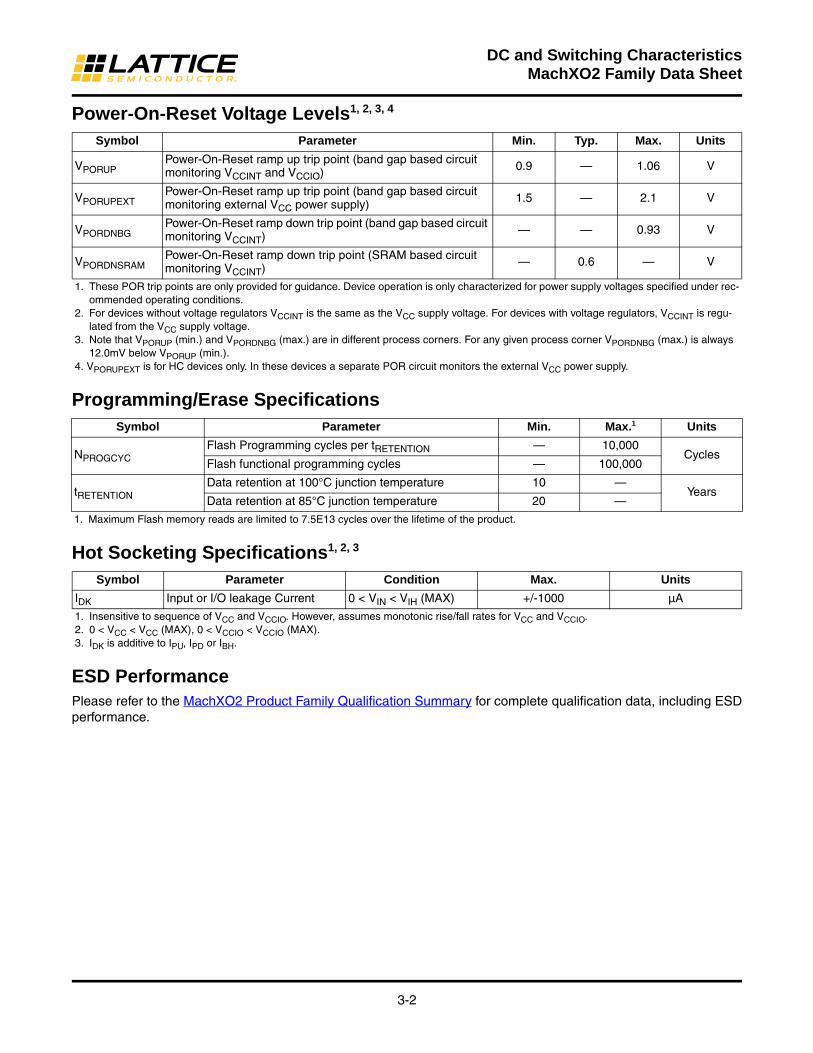
3-2
DC and Switching CharacteristicsMachXO2 Family Data Sheet
Power-On-Reset Voltage Levels1, 2, 3, 4
Programming/Erase Specifications
Hot Socketing Specifications1, 2, 3
ESD PerformancePlease refer to the MachXO2 Product Family Qualification Summary for complete qualification data, including ESD performance.
Symbol Parameter Min. Typ. Max. Units
VPORUPPower-On-Reset ramp up trip point (band gap based circuit monitoring VCCINT and VCCIO) 0.9 — 1.06 V
VPORUPEXTPower-On-Reset ramp up trip point (band gap based circuit monitoring external VCC power supply) 1.5 — 2.1 V
VPORDNBGPower-On-Reset ramp down trip point (band gap based circuit monitoring VCCINT) — — 0.93 V
VPORDNSRAMPower-On-Reset ramp down trip point (SRAM based circuit monitoring VCCINT) — 0.6 — V
1. These POR trip points are only provided for guidance. Device operation is only characterized for power supply voltages specified under rec-ommended operating conditions.
2. For devices without voltage regulators VCCINT is the same as the VCC supply voltage. For devices with voltage regulators, VCCINT is regu-lated from the VCC supply voltage.
3. Note that VPORUP (min.) and VPORDNBG (max.) are in different process corners. For any given process corner VPORDNBG (max.) is always 12.0mV below VPORUP (min.).
4. VPORUPEXT is for HC devices only. In these devices a separate POR circuit monitors the external VCC power supply.
Symbol Parameter Min. Max.1 Units
NPROGCYCFlash Programming cycles per tRETENTION — 10,000
CyclesFlash functional programming cycles — 100,000
tRETENTIONData retention at 100°C junction temperature 10 —
YearsData retention at 85°C junction temperature 20 —
1. Maximum Flash memory reads are limited to 7.5E13 cycles over the lifetime of the product.
Symbol Parameter Condition Max. Units
IDK Input or I/O leakage Current 0 < VIN < VIH (MAX) +/-1000 µA
1. Insensitive to sequence of VCC and VCCIO. However, assumes monotonic rise/fall rates for VCC and VCCIO.2. 0 < VCC < VCC (MAX), 0 < VCCIO < VCCIO (MAX). 3. IDK is additive to IPU, IPD or IBH.

3-3
DC and Switching CharacteristicsMachXO2 Family Data Sheet
DC Electrical CharacteristicsOver Recommended Operating Conditions
Symbol Parameter Condition Min. Typ. Max. Units
IIL, IIH1, 4 Input or I/O Leakage
Clamp OFF and VCCIO < VIN < VIH (MAX) — — +175 µA
Clamp OFF and VIN = VCCIO -10 — 10 µA
Clamp OFF and VCCIO * 0.6 < VIN < VCCIO
-175 — — µA
Clamp OFF and 0V < VIN < VCCIO * 0.6 — — 10 µA
Clamp OFF and VIN = GND — — 10 µA
Clamp ON and 0V < VIN < VCCIO — — 10 µA
IPU I/O Active Pull-up Current 0 < VIN < 0.7 VCCIO -30 — -309 µA
IPDI/O Active Pull-down Current VIL (MAX) < VIN < VCCIO 30 — 305 µA
IBHLSBus Hold Low sustaining current VIN = VIL (MAX) 30 — — µA
IBHHSBus Hold High sustaining current VIN = 0.7VCCIO -30 — — µA
IBHLOBus Hold Low Overdrive current 0 VIN VCCIO — — 305 µA
IBHHOBus Hold High Overdrive current 0 VIN VCCIO — — -309 µA
VBHT3 Bus Hold Trip Points VIL
(MAX) — VIH (MIN) V
C1 I/O Capacitance2 VCCIO = 3.3V, 2.5V, 1.8V, 1.5V, 1.2V,VCC = Typ., VIO = 0 to VIH (MAX) 3 5 9 pf
C2 Dedicated Input Capacitance2
VCCIO = 3.3V, 2.5V, 1.8V, 1.5V, 1.2V,VCC = Typ., VIO = 0 to VIH (MAX) 3 5.5 7 pf
VHYSTHysteresis for Schmitt Trigger Inputs5
VCCIO = 3.3V, Hysteresis = Large — 450 — mV
VCCIO = 2.5V, Hysteresis = Large — 250 — mV
VCCIO = 1.8V, Hysteresis = Large — 125 — mV
VCCIO = 1.5V, Hysteresis = Large — 100 — mV
VCCIO = 3.3V, Hysteresis = Small — 250 — mV
VCCIO = 2.5V, Hysteresis = Small — 150 — mV
VCCIO = 1.8V, Hysteresis = Small — 60 — mV
VCCIO = 1.5V, Hysteresis = Small — 40 — mV
1. Input or I/O leakage current is measured with the pin configured as an input or as an I/O with the output driver tri-stated. It is not measured with the output driver active. Bus maintenance circuits are disabled.
2. TA 25°C, f = 1.0MHz.3. Please refer to VIL and VIH in the sysIO Single-Ended DC Electrical Characteristics table of this document.4. When VIH is higher than VCCIO, a transient current typically of 30ns in duration or less with a peak current of 6mA can occur on the high-to-
low transition. For true LVDS output pins in MachXO2-640U, MachXO2-1200/U and larger devices, VIH must be less than or equal to VCCIO.5. With bus keeper circuit turned on. For more details, refer to TN1202, MachXO2 sysIO Usage Guide.

3-4
DC and Switching CharacteristicsMachXO2 Family Data Sheet
Static Supply Current – ZE Devices1, 2, 3, 6
Static Power Consumption Contribution of Different Components – ZE DevicesThe table below can be used for approximating static power consumption. For a more accurate power analysis for your design please use the Power Calculator tool.
Symbol Parameter Device Typ.4 Units
ICC Core Power Supply
LCMXO2-256ZE 18 µA
LCMXO2-640ZE 28 µA
LCMXO2-1200ZE 56 µA
LCMXO2-2000ZE 80 µA
LCMXO2-4000ZE 124 µA
LCMXO2-7000ZE 189 µA
ICCIOBank Power Supply5
VCCIO = 2.5V All devices 0 mA
1. For further information on supply current, please refer to TN1198, Power Estimation and Management for MachXO2 Devices.2. Assumes blank pattern with the following characteristics: all outputs are tri-stated, all inputs are configured as LVCMOS and held at VCCIO
or GND, on-chip oscillator is off, on-chip PLL is off. To estimate the impact of turning each of these items on, please refer to the following table or for more detail with your specific design use the Power Calculator tool.
3. Frequency = 0 MHz.4. TJ = 25°C, power supplies at nominal voltage.5. Does not include pull-up/pull-down.6. To determine the MachXO2 peak start-up current data, use the Power Calculator tool.
Symbol Parameter Typ. Units
IDCBG Bandgap DC power contribution 101 µA
IDCPOR POR DC power contribution 38 µA
IDCIOBANKCONTROLLER DC power contribution per I/O bank controller 143 µA
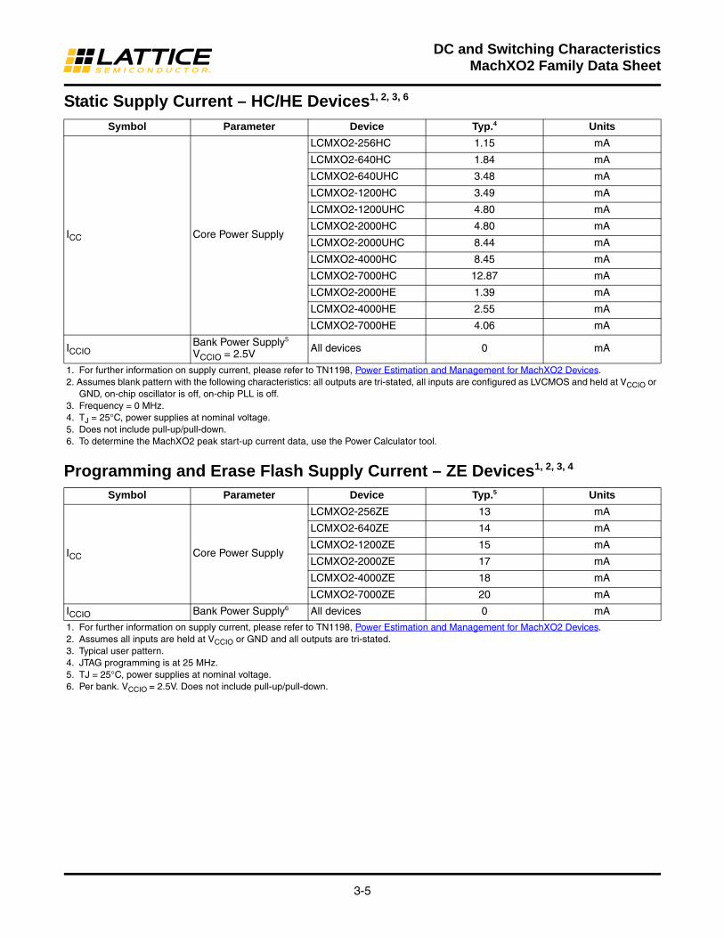
3-5
DC and Switching CharacteristicsMachXO2 Family Data Sheet
Static Supply Current – HC/HE Devices1, 2, 3, 6
Programming and Erase Flash Supply Current – ZE Devices1, 2, 3, 4
Symbol Parameter Device Typ.4 Units
ICC Core Power Supply
LCMXO2-256HC 1.15 mA
LCMXO2-640HC 1.84 mA
LCMXO2-640UHC 3.48 mA
LCMXO2-1200HC 3.49 mA
LCMXO2-1200UHC 4.80 mA
LCMXO2-2000HC 4.80 mA
LCMXO2-2000UHC 8.44 mA
LCMXO2-4000HC 8.45 mA
LCMXO2-7000HC 12.87 mA
LCMXO2-2000HE 1.39 mA
LCMXO2-4000HE 2.55 mA
LCMXO2-7000HE 4.06 mA
ICCIOBank Power Supply5
VCCIO = 2.5V All devices 0 mA
1. For further information on supply current, please refer to TN1198, Power Estimation and Management for MachXO2 Devices.2. Assumes blank pattern with the following characteristics: all outputs are tri-stated, all inputs are configured as LVCMOS and held at VCCIO or
GND, on-chip oscillator is off, on-chip PLL is off.3. Frequency = 0 MHz.4. TJ = 25°C, power supplies at nominal voltage.5. Does not include pull-up/pull-down.6. To determine the MachXO2 peak start-up current data, use the Power Calculator tool.
Symbol Parameter Device Typ.5 Units
ICC Core Power Supply
LCMXO2-256ZE 13 mA
LCMXO2-640ZE 14 mA
LCMXO2-1200ZE 15 mA
LCMXO2-2000ZE 17 mA
LCMXO2-4000ZE 18 mA
LCMXO2-7000ZE 20 mA
ICCIO Bank Power Supply6 All devices 0 mA
1. For further information on supply current, please refer to TN1198, Power Estimation and Management for MachXO2 Devices.2. Assumes all inputs are held at VCCIO or GND and all outputs are tri-stated.3. Typical user pattern.4. JTAG programming is at 25 MHz.5. TJ = 25°C, power supplies at nominal voltage.6. Per bank. VCCIO = 2.5V. Does not include pull-up/pull-down.
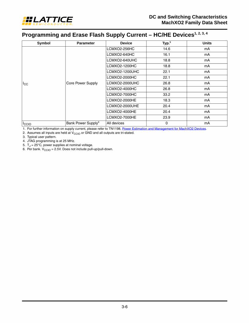
3-6
DC and Switching CharacteristicsMachXO2 Family Data Sheet
Programming and Erase Flash Supply Current – HC/HE Devices1, 2, 3, 4
Symbol Parameter Device Typ.5 Units
ICC Core Power Supply
LCMXO2-256HC 14.6 mA
LCMXO2-640HC 16.1 mA
LCMXO2-640UHC 18.8 mA
LCMXO2-1200HC 18.8 mA
LCMXO2-1200UHC 22.1 mA
LCMXO2-2000HC 22.1 mA
LCMXO2-2000UHC 26.8 mA
LCMXO2-4000HC 26.8 mA
LCMXO2-7000HC 33.2 mA
LCMXO2-2000HE 18.3 mA
LCMXO2-2000UHE 20.4 mA
LCMXO2-4000HE 20.4 mA
LCMXO2-7000HE 23.9 mA
ICCIO Bank Power Supply6 All devices 0 mA
1. For further information on supply current, please refer to TN1198, Power Estimation and Management for MachXO2 Devices.2. Assumes all inputs are held at VCCIO or GND and all outputs are tri-stated.3. Typical user pattern.4. JTAG programming is at 25 MHz.5. TJ = 25°C, power supplies at nominal voltage.6. Per bank. VCCIO = 2.5V. Does not include pull-up/pull-down.
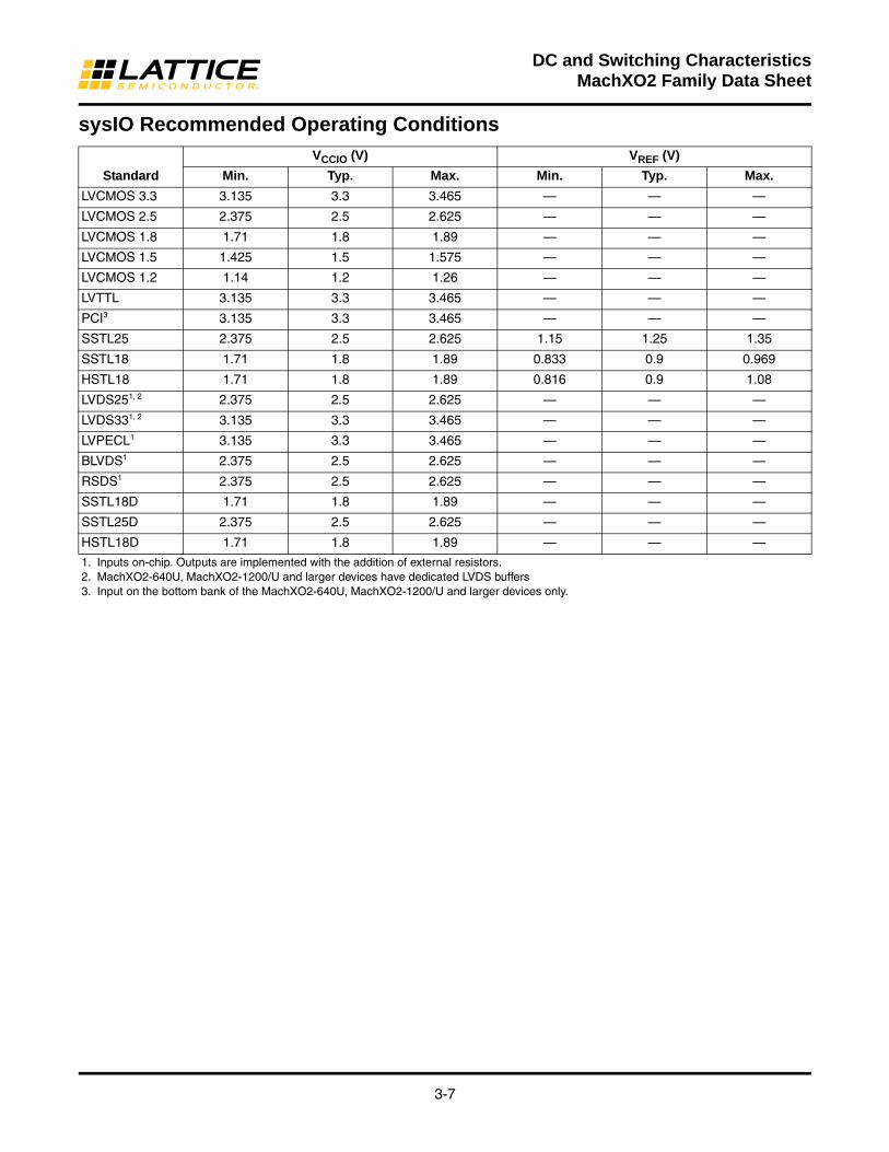
3-7
DC and Switching CharacteristicsMachXO2 Family Data Sheet
sysIO Recommended Operating Conditions
Standard
VCCIO (V) VREF (V)
Min. Typ. Max. Min. Typ. Max.
LVCMOS 3.3 3.135 3.3 3.465 — — —
LVCMOS 2.5 2.375 2.5 2.625 — — —
LVCMOS 1.8 1.71 1.8 1.89 — — —
LVCMOS 1.5 1.425 1.5 1.575 — — —
LVCMOS 1.2 1.14 1.2 1.26 — — —
LVTTL 3.135 3.3 3.465 — — —
PCI3 3.135 3.3 3.465 — — —
SSTL25 2.375 2.5 2.625 1.15 1.25 1.35
SSTL18 1.71 1.8 1.89 0.833 0.9 0.969
HSTL18 1.71 1.8 1.89 0.816 0.9 1.08
LVDS251, 2 2.375 2.5 2.625 — — —
LVDS331, 2 3.135 3.3 3.465 — — —
LVPECL1 3.135 3.3 3.465 — — —
BLVDS1 2.375 2.5 2.625 — — —
RSDS1 2.375 2.5 2.625 — — —
SSTL18D 1.71 1.8 1.89 — — —
SSTL25D 2.375 2.5 2.625 — — —
HSTL18D 1.71 1.8 1.89 — — —
1. Inputs on-chip. Outputs are implemented with the addition of external resistors.2. MachXO2-640U, MachXO2-1200/U and larger devices have dedicated LVDS buffers3. Input on the bottom bank of the MachXO2-640U, MachXO2-1200/U and larger devices only.

3-8
DC and Switching CharacteristicsMachXO2 Family Data Sheet
sysIO Single-Ended DC Electrical Characteristics1, 2
Input/Output Standard
VIL VIH VOL Max. (V)
VOH Min. (V)
IOL Max.4
(mA)IOH Max.4
(mA)Min. (V)3 Max. (V) Min. (V) Max. (V)
LVCMOS 3.3LVTTL -0.3 0.8 2.0 3.6
0.4 VCCIO - 0.4
4 -4
8 -8
12 -12
16 -16
24 -24
0.2 VCCIO - 0.2 0.1 -0.1
LVCMOS 2.5 -0.3 0.7 1.7 3.60.4 VCCIO - 0.4
4 -4
8 -8
12 -12
16 -16
0.2 VCCIO - 0.2 0.1 -0.1
LVCMOS 1.8 -0.3 0.35VCCIO 0.65VCCIO 3.60.4 VCCIO - 0.4
4 -4
8 -8
12 -12
0.2 VCCIO - 0.2 0.1 -0.1
LVCMOS 1.5 -0.3 0.35VCCIO 0.65VCCIO 3.60.4 VCCIO - 0.4
4 -4
8 -8
0.2 VCCIO - 0.2 0.1 -0.1
LVCMOS 1.2 -0.3 0.35VCCIO 0.65VCCIO 3.60.4 VCCIO - 0.4
4 -2
8 -6
0.2 VCCIO - 0.2 0.1 -0.1
PCI -0.3 0.3VCCIO 0.5VCCIO 3.6 0.1VCCIO 0.9VCCIO 1.5 -0.5
SSTL25 Class I -0.3 VREF - 0.18 VREF + 0.18 3.6 0.54 VCCIO - 0.62 8 8
SSTL25 Class II -0.3 VREF - 0.18 VREF +0.18 3.6 NA NA NA NA
SSTL18 Class I -0.3 VREF - 0.125 VREF +0.125 3.6 0.40 VCCIO - 0.40 8 8
SSTL18 Class II -0.3 VREF - 0.125 VREF +0.125 3.6 NA NA NA NA
HSTL18 Class I -0.3 VREF - 0.1 VREF +0.1 3.6 0.40 VCCIO - 0.40 8 8
HSTL18 Class II -0.3 VREF - 0.1 VREF +0.1 3.6 NA NA NA NA
1. MachXO2 devices allow LVCMOS inputs to be placed in I/O banks where VCCIO is different from what is specified in the applicable JEDEC specification. This is referred to as a ratioed input buffer. In a majority of cases this operation follows or exceeds the applicable JEDEC spec-ification. The cases where MachXO2 devices do not meet the relevant JEDEC specification are documented in the table below.
2. MachXO2 devices allow for LVCMOS referenced I/Os which follow applicable JEDEC specifications. For more details about mixed mode operation please refer to please refer to TN1202, MachXO2 sysIO Usage Guide.
3. The dual function I2C pins SCL and SDA are limited to a VIL min of -0.25V or to -0.3V with a duration of <10ns.4. The average DC current drawn by I/Os between GND connections, or between the last GND in an I/O bank and the end of an I/O bank, as
shown in the logic signal connections table shall not exceed n * 8mA. Where n is the number of I/Os between bank GND connections or between the last GND in a bank and the end of a bank.
Input Standard VCCIO (V) VIL Max. (V)
LVCMOS 33 1.5 0.685
LVCMOS 25 1.5 1.687
LVCMOS 18 1.5 1.164
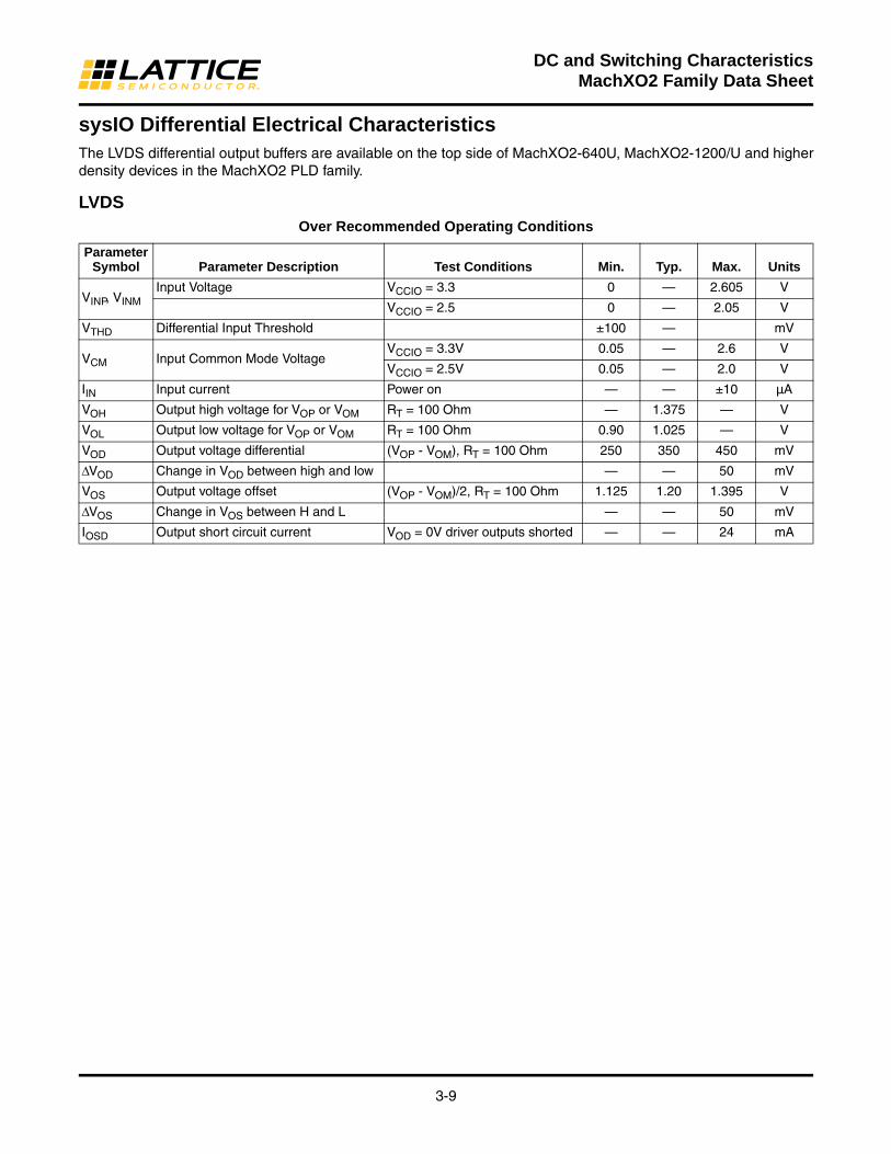
3-9
DC and Switching CharacteristicsMachXO2 Family Data Sheet
sysIO Differential Electrical CharacteristicsThe LVDS differential output buffers are available on the top side of MachXO2-640U, MachXO2-1200/U and higher density devices in the MachXO2 PLD family.
LVDSOver Recommended Operating Conditions
Parameter Symbol Parameter Description Test Conditions Min. Typ. Max. Units
VINP, VINMInput Voltage VCCIO = 3.3 0 — 2.605 V
VCCIO = 2.5 0 — 2.05 V
VTHD Differential Input Threshold ±100 — mV
VCM Input Common Mode VoltageVCCIO = 3.3V 0.05 — 2.6 V
VCCIO = 2.5V 0.05 — 2.0 V
IIN Input current Power on — — ±10 µA
VOH Output high voltage for VOP or VOM RT = 100 Ohm — 1.375 — V
VOL Output low voltage for VOP or VOM RT = 100 Ohm 0.90 1.025 — V
VOD Output voltage differential (VOP - VOM), RT = 100 Ohm 250 350 450 mV
VOD Change in VOD between high and low — — 50 mV
VOS Output voltage offset (VOP - VOM)/2, RT = 100 Ohm 1.125 1.20 1.395 V
VOS Change in VOS between H and L — — 50 mV
IOSD Output short circuit current VOD = 0V driver outputs shorted — — 24 mA

3-10
DC and Switching CharacteristicsMachXO2 Family Data Sheet
LVDS EmulationMachXO2 devices can support LVDS outputs via emulation (LVDS25E). The output is emulated using complemen-tary LVCMOS outputs in conjunction with resistors across the driver outputs on all devices. The scheme shown in Figure 3-1 is one possible solution for LVDS standard implementation. Resistor values in Figure 3-1 are industry standard values for 1% resistors.
Figure 3-1. LVDS Using External Resistors (LVDS25E)
Table 3-1. LVDS25E DC Conditions
Over Recommended Operating Conditions
Parameter Description Typ. Units
ZOUT Output impedance 20 Ohms
RS Driver series resistor 158 Ohms
RP Driver parallel resistor 140 Ohms
RT Receiver termination 100 Ohms
VOH Output high voltage 1.43 V
VOL Output low voltage 1.07 V
VOD Output differential voltage 0.35 V
VCM Output common mode voltage 1.25 V
ZBACK Back impedance 100.5 Ohms
IDC DC output current 6.03 mA
158
158
Zo = 100
140 100
On-chip On-chipOff-chip Off-chip
VCCIO = 2.5
8mA
8mA
Note: All resistors are ±1%.
VCCIO = 2.5 +
-
Emulated LVDS
Buffer

3-11
DC and Switching CharacteristicsMachXO2 Family Data Sheet
BLVDSThe MachXO2 family supports the BLVDS standard through emulation. The output is emulated using complemen-tary LVCMOS outputs in conjunction with resistors across the driver outputs. The input standard is supported by the LVDS differential input buffer. BLVDS is intended for use when multi-drop and bi-directional multi-point differen-tial signaling is required. The scheme shown in Figure 3-2 is one possible solution for bi-directional multi-point dif-ferential signals.
Figure 3-2. BLVDS Multi-point Output Example
Table 3-2. BLVDS DC Conditions1
Over Recommended Operating Conditions
Symbol Description
Nominal
UnitsZo = 45 Zo = 90
ZOUT Output impedance 10 10 Ohms
RS Driver series resistance 80 80 Ohms
RTLEFT Left end termination 45 90 Ohms
RTRIGHT Right end termination 45 90 Ohms
VOH Output high voltage 1.376 1.480 V
VOL Output low voltage 1.124 1.020 V
VOD Output differential voltage 0.253 0.459 V
VCM Output common mode voltage 1.250 1.250 V
IDC DC output current 11.236 10.204 mA
1. For input buffer, see LVDS table.
Heavily loaded backplane, effective Zo ~ 45 to 90 ohms differential
2.5V80
80
80808080
45-90 ohms 45-90 ohms
802.5V
2.5V
2.5V 2.5V 2.5V 2.5V
2.5V
+ -
. . . +
-
. . . + -
+ -
16mA
16mA 16mA 16mA 16mA
16mA
16mA16mA

3-12
DC and Switching CharacteristicsMachXO2 Family Data Sheet
LVPECLThe MachXO2 family supports the differential LVPECL standard through emulation. This output standard is emu-lated using complementary LVCMOS outputs in conjunction with resistors across the driver outputs on all the devices. The LVPECL input standard is supported by the LVDS differential input buffer. The scheme shown in Dif-ferential LVPECL is one possible solution for point-to-point signals.
Figure 3-3. Differential LVPECL
Table 3-3. LVPECL DC Conditions1
Over Recommended Operating Conditions
For further information on LVPECL, BLVDS and other differential interfaces please see details of additional techni-cal documentation at the end of the data sheet.
Symbol Description Nominal Units
ZOUT Output impedance 10 Ohms
RS Driver series resistor 93 Ohms
RP Driver parallel resistor 196 Ohms
RT Receiver termination 100 Ohms
VOH Output high voltage 2.05 V
VOL Output low voltage 1.25 V
VOD Output differential voltage 0.80 V
VCM Output common mode voltage 1.65 V
ZBACK Back impedance 100.5 Ohms
IDC DC output current 12.11 mA
1. For input buffer, see LVDS table.
Transmission line, Zo = 100 ohm differential
100 ohms
93 ohms16mA
16mA
93 ohms
Off-chip On-chip
VCCIO = 3.3V
VCCIO = 3.3V +
- 196 ohms
On-chip Off-chip
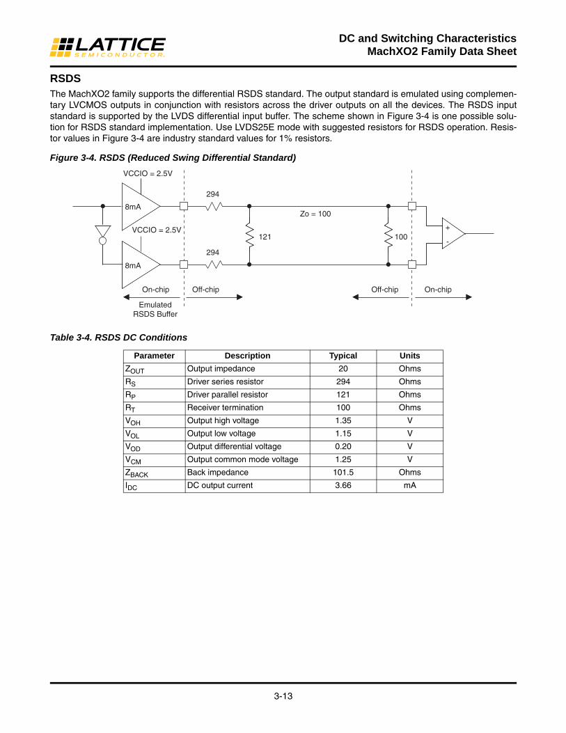
3-13
DC and Switching CharacteristicsMachXO2 Family Data Sheet
RSDSThe MachXO2 family supports the differential RSDS standard. The output standard is emulated using complemen-tary LVCMOS outputs in conjunction with resistors across the driver outputs on all the devices. The RSDS input standard is supported by the LVDS differential input buffer. The scheme shown in Figure 3-4 is one possible solu-tion for RSDS standard implementation. Use LVDS25E mode with suggested resistors for RSDS operation. Resis-tor values in Figure 3-4 are industry standard values for 1% resistors.
Figure 3-4. RSDS (Reduced Swing Differential Standard)
Table 3-4. RSDS DC Conditions
Parameter Description Typical Units
ZOUT Output impedance 20 Ohms
RS Driver series resistor 294 Ohms
RP Driver parallel resistor 121 Ohms
RT Receiver termination 100 Ohms
VOH Output high voltage 1.35 V
VOL Output low voltage 1.15 V
VOD Output differential voltage 0.20 V
VCM Output common mode voltage 1.25 V
ZBACK Back impedance 101.5 Ohms
IDC DC output current 3.66 mA
100
294
294
On-chip On-chipOff-chip
EmulatedRSDS Buffer
VCCIO = 2.5V
VCCIO = 2.5V
8mA
8mAZo = 100
+
-121
Off-chip

3-14
DC and Switching CharacteristicsMachXO2 Family Data Sheet
Typical Building Block Function Performance – HC/HE Devices1
Pin-to-Pin Performance (LVCMOS25 12mA Drive)
Register-to-Register Performance
Function -6 Timing Units
Basic Functions
16-bit decoder 8.9 ns
4:1 MUX 7.5 ns
16:1 MUX 8.3 ns
Function -6 Timing Units
Basic Functions
16:1 MUX 412 MHz
16-bit adder 297 MHz
16-bit counter 324 MHz
64-bit counter 161 MHz
Embedded Memory Functions
1024x9 True-Dual Port RAM (Write Through or Normal, EBR output registers) 183 MHz
Distributed Memory Functions
16x4 Pseudo-Dual Port RAM (one PFU) 500 MHz
1. The above timing numbers are generated using the Diamond design tool. Exact performance may vary with device and tool version. The tool uses internal parameters that have been characterized but are not tested on every device.

3-15
DC and Switching CharacteristicsMachXO2 Family Data Sheet
Typical Building Block Function Performance – ZE Devices1
Pin-to-Pin Performance (LVCMOS25 12mA Drive)
Register-to-Register Performance
Derating Logic TimingLogic timing provided in the following sections of the data sheet and the Lattice design tools are worst case num-bers in the operating range. Actual delays may be much faster. Lattice design tools can provide logic timing num-bers at a particular temperature and voltage.
Function -3 Timing Units
Basic Functions
16-bit decoder 13.9 ns
4:1 MUX 10.9 ns
16:1 MUX 12.0 ns
Function -3 Timing Units
Basic Functions
16:1 MUX 191 MHz
16-bit adder 134 MHz
16-bit counter 148 MHz
64-bit counter 77 MHz
Embedded Memory Functions
1024x9 True-Dual Port RAM (Write Through or Normal, EBR output registers) 90 MHz
Distributed Memory Functions
16x4 Pseudo-Dual Port RAM (one PFU) 214 MHz
1. The above timing numbers are generated using the Diamond design tool. Exact performance may vary with device and tool version. The tool uses internal parameters that have been characterized but are not tested on every device.
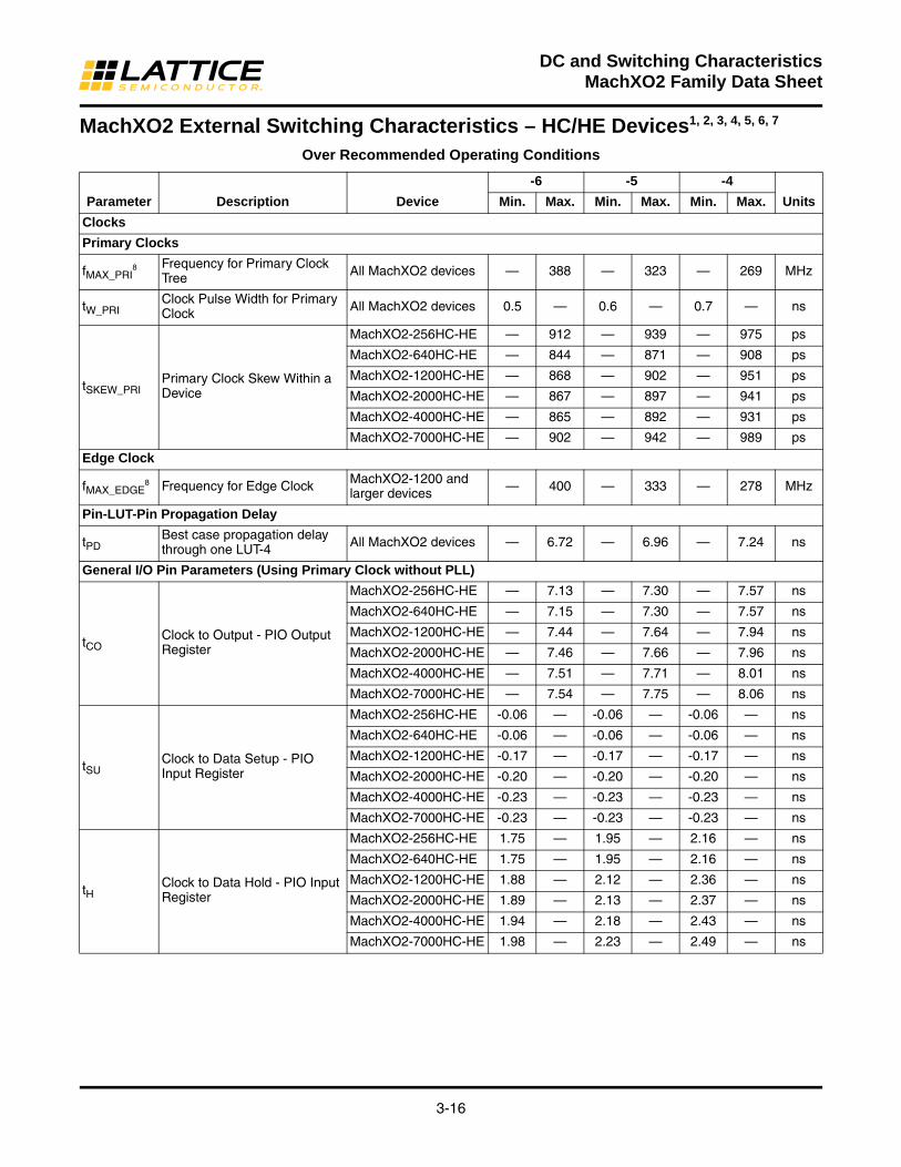
3-16
DC and Switching CharacteristicsMachXO2 Family Data Sheet
MachXO2 External Switching Characteristics – HC/HE Devices1, 2, 3, 4, 5, 6, 7
Over Recommended Operating Conditions
Parameter Description Device
-6 -5 -4
UnitsMin. Max. Min. Max. Min. Max.
Clocks
Primary Clocks
fMAX_PRI8 Frequency for Primary Clock
Tree All MachXO2 devices — 388 — 323 — 269 MHz
tW_PRIClock Pulse Width for Primary Clock All MachXO2 devices 0.5 — 0.6 — 0.7 — ns
tSKEW_PRIPrimary Clock Skew Within a Device
MachXO2-256HC-HE — 912 — 939 — 975 ps
MachXO2-640HC-HE — 844 — 871 — 908 ps
MachXO2-1200HC-HE — 868 — 902 — 951 ps
MachXO2-2000HC-HE — 867 — 897 — 941 ps
MachXO2-4000HC-HE — 865 — 892 — 931 ps
MachXO2-7000HC-HE — 902 — 942 — 989 ps
Edge Clock
fMAX_EDGE8 Frequency for Edge Clock MachXO2-1200 and
larger devices — 400 — 333 — 278 MHz
Pin-LUT-Pin Propagation Delay
tPDBest case propagation delay through one LUT-4 All MachXO2 devices — 6.72 — 6.96 — 7.24 ns
General I/O Pin Parameters (Using Primary Clock without PLL)
tCOClock to Output - PIO Output Register
MachXO2-256HC-HE — 7.13 — 7.30 — 7.57 ns
MachXO2-640HC-HE — 7.15 — 7.30 — 7.57 ns
MachXO2-1200HC-HE — 7.44 — 7.64 — 7.94 ns
MachXO2-2000HC-HE — 7.46 — 7.66 — 7.96 ns
MachXO2-4000HC-HE — 7.51 — 7.71 — 8.01 ns
MachXO2-7000HC-HE — 7.54 — 7.75 — 8.06 ns
tSUClock to Data Setup - PIO Input Register
MachXO2-256HC-HE -0.06 — -0.06 — -0.06 — ns
MachXO2-640HC-HE -0.06 — -0.06 — -0.06 — ns
MachXO2-1200HC-HE -0.17 — -0.17 — -0.17 — ns
MachXO2-2000HC-HE -0.20 — -0.20 — -0.20 — ns
MachXO2-4000HC-HE -0.23 — -0.23 — -0.23 — ns
MachXO2-7000HC-HE -0.23 — -0.23 — -0.23 — ns
tHClock to Data Hold - PIO Input Register
MachXO2-256HC-HE 1.75 — 1.95 — 2.16 — ns
MachXO2-640HC-HE 1.75 — 1.95 — 2.16 — ns
MachXO2-1200HC-HE 1.88 — 2.12 — 2.36 — ns
MachXO2-2000HC-HE 1.89 — 2.13 — 2.37 — ns
MachXO2-4000HC-HE 1.94 — 2.18 — 2.43 — ns
MachXO2-7000HC-HE 1.98 — 2.23 — 2.49 — ns

3-17
DC and Switching CharacteristicsMachXO2 Family Data Sheet
tSU_DEL
Clock to Data Setup - PIO Input Register with Data Input Delay
MachXO2-256HC-HE 1.42 — 1.59 — 1.96 — ns
MachXO2-640HC-HE 1.41 — 1.58 — 1.96 — ns
MachXO2-1200HC-HE 1.63 — 1.79 — 2.17 — ns
MachXO2-2000HC-HE 1.61 — 1.76 — 2.13 — ns
MachXO2-4000HC-HE 1.66 — 1.81 — 2.19 — ns
MachXO2-7000HC-HE 1.53 — 1.67 — 2.03 — ns
tH_DELClock to Data Hold - PIO Input Register with Input Data Delay
MachXO2-256HC-HE -0.24 — -0.24 — -0.24 — ns
MachXO2-640HC-HE -0.23 — -0.23 — -0.23 — ns
MachXO2-1200HC-HE -0.24 — -0.24 — -0.24 — ns
MachXO2-2000HC-HE -0.23 — -0.23 — -0.23 — ns
MachXO2-4000HC-HE -0.25 — -0.25 — -0.25 — ns
MachXO2-7000HC-HE -0.21 — -0.21 — -0.21 — ns
fMAX_IOClock Frequency of I/O and PFU Register All MachXO2 devices — 388 — 323 — 269 MHz
General I/O Pin Parameters (Using Edge Clock without PLL)
tCOEClock to Output - PIO Output Register
MachXO2-1200HC-HE — 7.53 — 7.76 — 8.10 ns
MachXO2-2000HC-HE — 7.53 — 7.76 — 8.10 ns
MachXO2-4000HC-HE — 7.45 — 7.68 — 8.00 ns
MachXO2-7000HC-HE — 7.53 — 7.76 — 8.10 ns
tSUEClock to Data Setup - PIO Input Register
MachXO2-1200HC-HE -0.19 — -0.19 — -0.19 — ns
MachXO2-2000HC-HE -0.19 — -0.19 — -0.19 — ns
MachXO2-4000HC-HE -0.16 — -0.16 — -0.16 — ns
MachXO2-7000HC-HE -0.19 — -0.19 — -0.19 — ns
tHEClock to Data Hold - PIO Input Register
MachXO2-1200HC-HE 1.97 — 2.24 — 2.52 — ns
MachXO2-2000HC-HE 1.97 — 2.24 — 2.52 — ns
MachXO2-4000HC-HE 1.89 — 2.16 — 2.43 — ns
MachXO2-7000HC-HE 1.97 — 2.24 — 2.52 — ns
tSU_DELE
Clock to Data Setup - PIO Input Register with Data Input Delay
MachXO2-1200HC-HE 1.56 — 1.69 — 2.05 — ns
MachXO2-2000HC-HE 1.56 — 1.69 — 2.05 — ns
MachXO2-4000HC-HE 1.74 — 1.88 — 2.25 — ns
MachXO2-7000HC-HE 1.66 — 1.81 — 2.17 — ns
tH_DELEClock to Data Hold - PIO Input Register with Input Data Delay
MachXO2-1200HC-HE -0.23 — -0.23 — -0.23 — ns
MachXO2-2000HC-HE -0.23 — -0.23 — -0.23 — ns
MachXO2-4000HC-HE -0.34 — -0.34 — -0.34 — ns
MachXO2-7000HC-HE -0.29 — -0.29 — -0.29 — ns
General I/O Pin Parameters (Using Primary Clock with PLL)
tCOPLLClock to Output - PIO Output Register
MachXO2-1200HC-HE — 5.97 — 6.00 — 6.13 ns
MachXO2-2000HC-HE — 5.98 — 6.01 — 6.14 ns
MachXO2-4000HC-HE — 5.99 — 6.02 — 6.16 ns
MachXO2-7000HC-HE — 6.02 — 6.06 — 6.20 ns
tSUPLLClock to Data Setup - PIO Input Register
MachXO2-1200HC-HE 0.36 — 0.36 — 0.65 — ns
MachXO2-2000HC-HE 0.36 — 0.36 — 0.63 — ns
MachXO2-4000HC-HE 0.35 — 0.35 — 0.62 — ns
MachXO2-7000HC-HE 0.34 — 0.34 — 0.59 — ns
Parameter Description Device
-6 -5 -4
UnitsMin. Max. Min. Max. Min. Max.

3-18
DC and Switching CharacteristicsMachXO2 Family Data Sheet
tHPLLClock to Data Hold - PIO Input Register
MachXO2-1200HC-HE 0.41 — 0.48 — 0.55 — ns
MachXO2-2000HC-HE 0.42 — 0.49 — 0.56 — ns
MachXO2-4000HC-HE 0.43 — 0.50 — 0.58 — ns
MachXO2-7000HC-HE 0.46 — 0.54 — 0.62 — ns
tSU_DELPLL
Clock to Data Setup - PIO Input Register with Data Input Delay
MachXO2-1200HC-HE 2.88 — 3.19 — 3.72 — ns
MachXO2-2000HC-HE 2.87 — 3.18 — 3.70 — ns
MachXO2-4000HC-HE 2.96 — 3.28 — 3.81 — ns
MachXO2-7000HC-HE 3.05 — 3.35 — 3.87 — ns
tH_DELPLLClock to Data Hold - PIO Input Register with Input Data Delay
MachXO2-1200HC-HE -0.83 — -0.83 — -0.83 — ns
MachXO2-2000HC-HE -0.83 — -0.83 — -0.83 — ns
MachXO2-4000HC-HE -0.87 — -0.87 — -0.87 — ns
MachXO2-7000HC-HE -0.91 — -0.91 — -0.91 — ns
Generic DDRX1 Inputs with Clock and Data Aligned at Pin Using PCLK Pin for Clock Input – GDDRX1_RX.SCLK.Aligned9
tDVA Input Data Valid After CLK
All MachXO2 devices, all sides
— 0.317 — 0.344 — 0.368 UI
tDVE Input Data Hold After CLK 0.742 — 0.702 — 0.668 — UI
fDATA DDRX1 Input Data Speed — 300 — 250 — 208 Mbps
fDDRX1 DDRX1 SCLK Frequency — 150 — 125 — 104 MHz
Generic DDRX1 Inputs with Clock and Data Centered at Pin Using PCLK Pin for Clock Input – GDDRX1_RX.SCLK.Centered9
tSU Input Data Setup Before CLK
All MachXO2 devices, all sides
0.566 — 0.560 — 0.538 — ns
tHO Input Data Hold After CLK 0.778 — 0.879 — 1.090 — ns
fDATA DDRX1 Input Data Speed — 300 — 250 — 208 Mbps
fDDRX1 DDRX1 SCLK Frequency — 150 — 125 — 104 MHz
Generic DDRX2 Inputs with Clock and Data Aligned at Pin Using PCLK Pin for Clock Input – GDDRX2_RX.ECLK.Aligned9
tDVA Input Data Valid After CLK
MachXO2-640U, MachXO2-1200/U and larger devices, bottom side only
— 0.316 — 0.342 — 0.364 UI
tDVE Input Data Hold After CLK 0.710 — 0.675 — 0.679 — UI
fDATADDRX2 Serial Input Data Speed — 664 — 554 — 462 Mbps
fDDRX2 DDRX2 ECLK Frequency — 332 — 277 — 231 MHz
fSCLK SCLK Frequency — 166 — 139 — 116 MHz
Generic DDRX2 Inputs with Clock and Data Centered at Pin Using PCLK Pin for Clock Input – GDDRX2_RX.ECLK.Centered9
tSU Input Data Setup Before CLK
MachXO2-640U, MachXO2-1200/U and larger devices, bottom side only
0.233 — 0.219 — 0.198 — ns
tHO Input Data Hold After CLK 0.287 — 0.287 — 0.344 — ns
fDATADDRX2 Serial Input Data Speed — 664 — 554 — 462 Mbps
fDDRX2 DDRX2 ECLK Frequency — 332 — 277 — 231 MHz
fSCLK SCLK Frequency — 166 — 139 — 116 MHz
Parameter Description Device
-6 -5 -4
UnitsMin. Max. Min. Max. Min. Max.
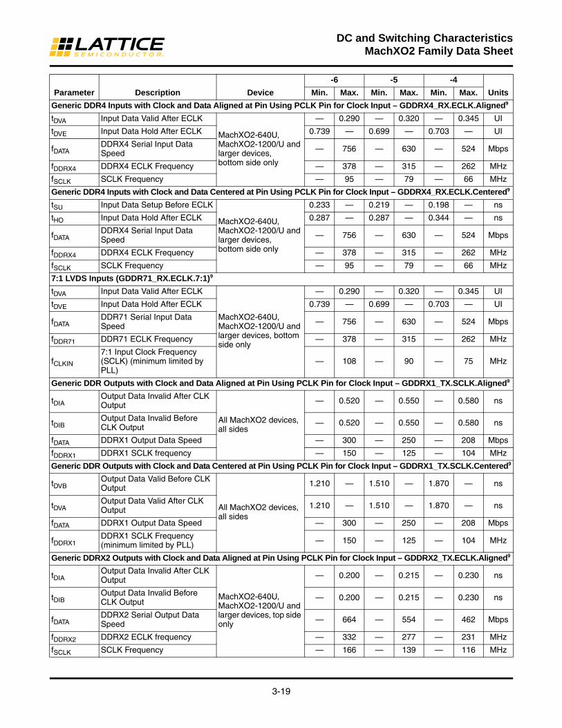
3-19
DC and Switching CharacteristicsMachXO2 Family Data Sheet
Generic DDR4 Inputs with Clock and Data Aligned at Pin Using PCLK Pin for Clock Input – GDDRX4_RX.ECLK.Aligned9
tDVA Input Data Valid After ECLK
MachXO2-640U, MachXO2-1200/U and larger devices, bottom side only
— 0.290 — 0.320 — 0.345 UI
tDVE Input Data Hold After ECLK 0.739 — 0.699 — 0.703 — UI
fDATADDRX4 Serial Input Data Speed — 756 — 630 — 524 Mbps
fDDRX4 DDRX4 ECLK Frequency — 378 — 315 — 262 MHz
fSCLK SCLK Frequency — 95 — 79 — 66 MHz
Generic DDR4 Inputs with Clock and Data Centered at Pin Using PCLK Pin for Clock Input – GDDRX4_RX.ECLK.Centered9
tSU Input Data Setup Before ECLK
MachXO2-640U, MachXO2-1200/U and larger devices, bottom side only
0.233 — 0.219 — 0.198 — ns
tHO Input Data Hold After ECLK 0.287 — 0.287 — 0.344 — ns
fDATADDRX4 Serial Input Data Speed — 756 — 630 — 524 Mbps
fDDRX4 DDRX4 ECLK Frequency — 378 — 315 — 262 MHz
fSCLK SCLK Frequency — 95 — 79 — 66 MHz
7:1 LVDS Inputs (GDDR71_RX.ECLK.7:1)9
tDVA Input Data Valid After ECLK
MachXO2-640U, MachXO2-1200/U and larger devices, bottom side only
— 0.290 — 0.320 — 0.345 UI
tDVE Input Data Hold After ECLK 0.739 — 0.699 — 0.703 — UI
fDATADDR71 Serial Input Data Speed — 756 — 630 — 524 Mbps
fDDR71 DDR71 ECLK Frequency — 378 — 315 — 262 MHz
fCLKIN
7:1 Input Clock Frequency (SCLK) (minimum limited by PLL)
— 108 — 90 — 75 MHz
Generic DDR Outputs with Clock and Data Aligned at Pin Using PCLK Pin for Clock Input – GDDRX1_TX.SCLK.Aligned9
tDIAOutput Data Invalid After CLK Output
All MachXO2 devices, all sides
— 0.520 — 0.550 — 0.580 ns
tDIBOutput Data Invalid Before CLK Output — 0.520 — 0.550 — 0.580 ns
fDATA DDRX1 Output Data Speed — 300 — 250 — 208 Mbps
fDDRX1 DDRX1 SCLK frequency — 150 — 125 — 104 MHz
Generic DDR Outputs with Clock and Data Centered at Pin Using PCLK Pin for Clock Input – GDDRX1_TX.SCLK.Centered9
tDVBOutput Data Valid Before CLK Output
All MachXO2 devices, all sides
1.210 — 1.510 — 1.870 — ns
tDVAOutput Data Valid After CLK Output 1.210 — 1.510 — 1.870 — ns
fDATA DDRX1 Output Data Speed — 300 — 250 — 208 Mbps
fDDRX1DDRX1 SCLK Frequency(minimum limited by PLL) — 150 — 125 — 104 MHz
Generic DDRX2 Outputs with Clock and Data Aligned at Pin Using PCLK Pin for Clock Input – GDDRX2_TX.ECLK.Aligned9
tDIAOutput Data Invalid After CLK Output
MachXO2-640U, MachXO2-1200/U and larger devices, top side only
— 0.200 — 0.215 — 0.230 ns
tDIBOutput Data Invalid Before CLK Output — 0.200 — 0.215 — 0.230 ns
fDATADDRX2 Serial Output Data Speed — 664 — 554 — 462 Mbps
fDDRX2 DDRX2 ECLK frequency — 332 — 277 — 231 MHz
fSCLK SCLK Frequency — 166 — 139 — 116 MHz
Parameter Description Device
-6 -5 -4
UnitsMin. Max. Min. Max. Min. Max.
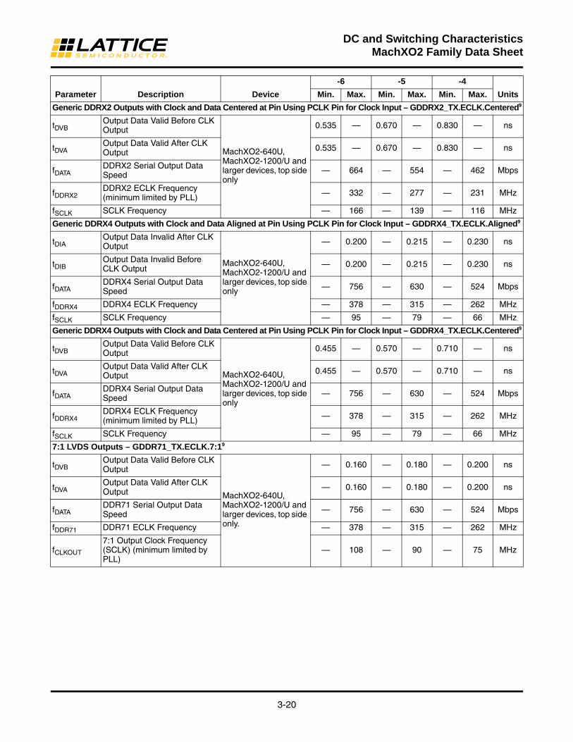
3-20
DC and Switching CharacteristicsMachXO2 Family Data Sheet
Generic DDRX2 Outputs with Clock and Data Centered at Pin Using PCLK Pin for Clock Input – GDDRX2_TX.ECLK.Centered9
tDVBOutput Data Valid Before CLK Output
MachXO2-640U, MachXO2-1200/U and larger devices, top side only
0.535 — 0.670 — 0.830 — ns
tDVAOutput Data Valid After CLK Output 0.535 — 0.670 — 0.830 — ns
fDATADDRX2 Serial Output Data Speed — 664 — 554 — 462 Mbps
fDDRX2DDRX2 ECLK Frequency(minimum limited by PLL) — 332 — 277 — 231 MHz
fSCLK SCLK Frequency — 166 — 139 — 116 MHz
Generic DDRX4 Outputs with Clock and Data Aligned at Pin Using PCLK Pin for Clock Input – GDDRX4_TX.ECLK.Aligned9
tDIAOutput Data Invalid After CLK Output
MachXO2-640U, MachXO2-1200/U and larger devices, top side only
— 0.200 — 0.215 — 0.230 ns
tDIBOutput Data Invalid Before CLK Output — 0.200 — 0.215 — 0.230 ns
fDATADDRX4 Serial Output Data Speed — 756 — 630 — 524 Mbps
fDDRX4 DDRX4 ECLK Frequency — 378 — 315 — 262 MHz
fSCLK SCLK Frequency — 95 — 79 — 66 MHz
Generic DDRX4 Outputs with Clock and Data Centered at Pin Using PCLK Pin for Clock Input – GDDRX4_TX.ECLK.Centered9
tDVBOutput Data Valid Before CLK Output
MachXO2-640U, MachXO2-1200/U and larger devices, top side only
0.455 — 0.570 — 0.710 — ns
tDVAOutput Data Valid After CLK Output 0.455 — 0.570 — 0.710 — ns
fDATADDRX4 Serial Output Data Speed — 756 — 630 — 524 Mbps
fDDRX4DDRX4 ECLK Frequency (minimum limited by PLL) — 378 — 315 — 262 MHz
fSCLK SCLK Frequency — 95 — 79 — 66 MHz
7:1 LVDS Outputs – GDDR71_TX.ECLK.7:19
tDVBOutput Data Valid Before CLK Output
MachXO2-640U, MachXO2-1200/U and larger devices, top side only.
— 0.160 — 0.180 — 0.200 ns
tDVAOutput Data Valid After CLK Output — 0.160 — 0.180 — 0.200 ns
fDATADDR71 Serial Output Data Speed — 756 — 630 — 524 Mbps
fDDR71 DDR71 ECLK Frequency — 378 — 315 — 262 MHz
fCLKOUT
7:1 Output Clock Frequency (SCLK) (minimum limited by PLL)
— 108 — 90 — 75 MHz
Parameter Description Device
-6 -5 -4
UnitsMin. Max. Min. Max. Min. Max.
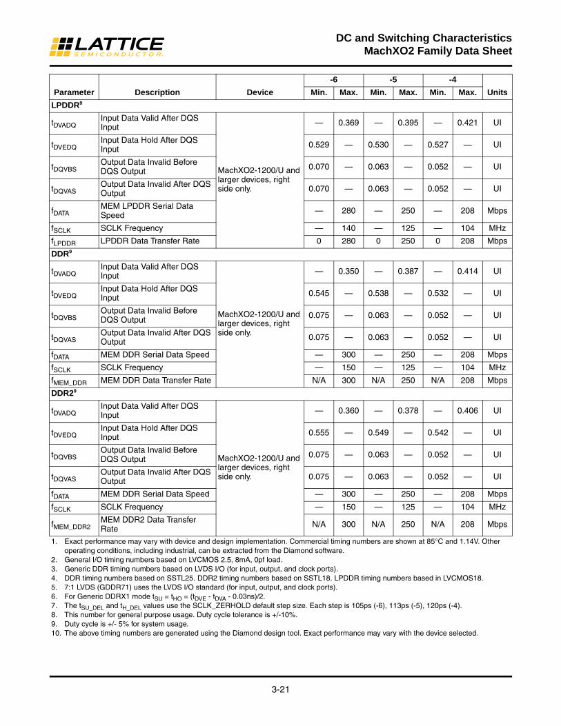
3-21
DC and Switching CharacteristicsMachXO2 Family Data Sheet
LPDDR9
tDVADQInput Data Valid After DQS Input
MachXO2-1200/U and larger devices, right side only.
— 0.369 — 0.395 — 0.421 UI
tDVEDQInput Data Hold After DQS Input 0.529 — 0.530 — 0.527 — UI
tDQVBSOutput Data Invalid Before DQS Output 0.070 — 0.063 — 0.052 — UI
tDQVASOutput Data Invalid After DQS Output 0.070 — 0.063 — 0.052 — UI
fDATAMEM LPDDR Serial Data Speed — 280 — 250 — 208 Mbps
fSCLK SCLK Frequency — 140 — 125 — 104 MHz
fLPDDR LPDDR Data Transfer Rate 0 280 0 250 0 208 Mbps
DDR9
tDVADQInput Data Valid After DQS Input
MachXO2-1200/U and larger devices, right side only.
— 0.350 — 0.387 — 0.414 UI
tDVEDQInput Data Hold After DQS Input 0.545 — 0.538 — 0.532 — UI
tDQVBSOutput Data Invalid Before DQS Output 0.075 — 0.063 — 0.052 — UI
tDQVASOutput Data Invalid After DQS Output 0.075 — 0.063 — 0.052 — UI
fDATA MEM DDR Serial Data Speed — 300 — 250 — 208 Mbps
fSCLK SCLK Frequency — 150 — 125 — 104 MHz
fMEM_DDR MEM DDR Data Transfer Rate N/A 300 N/A 250 N/A 208 Mbps
DDR29
tDVADQInput Data Valid After DQS Input
MachXO2-1200/U and larger devices, right side only.
— 0.360 — 0.378 — 0.406 UI
tDVEDQInput Data Hold After DQS Input 0.555 — 0.549 — 0.542 — UI
tDQVBSOutput Data Invalid Before DQS Output 0.075 — 0.063 — 0.052 — UI
tDQVASOutput Data Invalid After DQS Output 0.075 — 0.063 — 0.052 — UI
fDATA MEM DDR Serial Data Speed — 300 — 250 — 208 Mbps
fSCLK SCLK Frequency — 150 — 125 — 104 MHz
fMEM_DDR2MEM DDR2 Data Transfer Rate N/A 300 N/A 250 N/A 208 Mbps
1. Exact performance may vary with device and design implementation. Commercial timing numbers are shown at 85°C and 1.14V. Other operating conditions, including industrial, can be extracted from the Diamond software.
2. General I/O timing numbers based on LVCMOS 2.5, 8mA, 0pf load.3. Generic DDR timing numbers based on LVDS I/O (for input, output, and clock ports).4. DDR timing numbers based on SSTL25. DDR2 timing numbers based on SSTL18. LPDDR timing numbers based in LVCMOS18.5. 7:1 LVDS (GDDR71) uses the LVDS I/O standard (for input, output, and clock ports).6. For Generic DDRX1 mode tSU = tHO = (tDVE - tDVA - 0.03ns)/2.7. The tSU_DEL and tH_DEL values use the SCLK_ZERHOLD default step size. Each step is 105ps (-6), 113ps (-5), 120ps (-4).8. This number for general purpose usage. Duty cycle tolerance is +/-10%.9. Duty cycle is +/- 5% for system usage.10. The above timing numbers are generated using the Diamond design tool. Exact performance may vary with the device selected.
Parameter Description Device
-6 -5 -4
UnitsMin. Max. Min. Max. Min. Max.
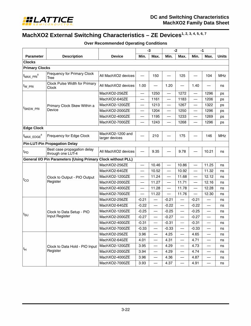
3-22
DC and Switching CharacteristicsMachXO2 Family Data Sheet
MachXO2 External Switching Characteristics – ZE Devices1, 2, 3, 4, 5, 6, 7
Over Recommended Operating Conditions
Parameter Description Device
-3 -2 -1
UnitsMin. Max. Min. Max. Min. Max.
Clocks
Primary Clocks
fMAX_PRI8 Frequency for Primary Clock
Tree All MachXO2 devices — 150 — 125 — 104 MHz
tW_PRIClock Pulse Width for Primary Clock All MachXO2 devices 1.00 — 1.20 — 1.40 — ns
tSKEW_PRIPrimary Clock Skew Within a Device
MachXO2-256ZE — 1250 — 1272 — 1296 ps
MachXO2-640ZE — 1161 — 1183 — 1206 ps
MachXO2-1200ZE — 1213 — 1267 — 1322 ps
MachXO2-2000ZE — 1204 — 1250 — 1296 ps
MachXO2-4000ZE — 1195 — 1233 — 1269 ps
MachXO2-7000ZE — 1243 — 1268 — 1296 ps
Edge Clock
fMAX_EDGE8 Frequency for Edge Clock MachXO2-1200 and
larger devices — 210 — 175 — 146 MHz
Pin-LUT-Pin Propagation Delay
tPDBest case propagation delay through one LUT-4 All MachXO2 devices — 9.35 — 9.78 — 10.21 ns
General I/O Pin Parameters (Using Primary Clock without PLL)
tCOClock to Output - PIO Output Register
MachXO2-256ZE — 10.46 — 10.86 — 11.25 ns
MachXO2-640ZE — 10.52 — 10.92 — 11.32 ns
MachXO2-1200ZE — 11.24 — 11.68 — 12.12 ns
MachXO2-2000ZE — 11.27 — 11.71 — 12.16 ns
MachXO2-4000ZE — 11.28 — 11.78 — 12.28 ns
MachXO2-7000ZE — 11.22 — 11.76 — 12.30 ns
tSUClock to Data Setup - PIO Input Register
MachXO2-256ZE -0.21 — -0.21 — -0.21 — ns
MachXO2-640ZE -0.22 — -0.22 — -0.22 — ns
MachXO2-1200ZE -0.25 — -0.25 — -0.25 — ns
MachXO2-2000ZE -0.27 — -0.27 — -0.27 — ns
MachXO2-4000ZE -0.31 — -0.31 — -0.31 — ns
MachXO2-7000ZE -0.33 — -0.33 — -0.33 — ns
tHClock to Data Hold - PIO Input Register
MachXO2-256ZE 3.96 — 4.25 — 4.65 — ns
MachXO2-640ZE 4.01 — 4.31 — 4.71 — ns
MachXO2-1200ZE 3.95 — 4.29 — 4.73 — ns
MachXO2-2000ZE 3.94 — 4.29 — 4.74 — ns
MachXO2-4000ZE 3.96 — 4.36 — 4.87 — ns
MachXO2-7000ZE 3.93 — 4.37 — 4.91 — ns
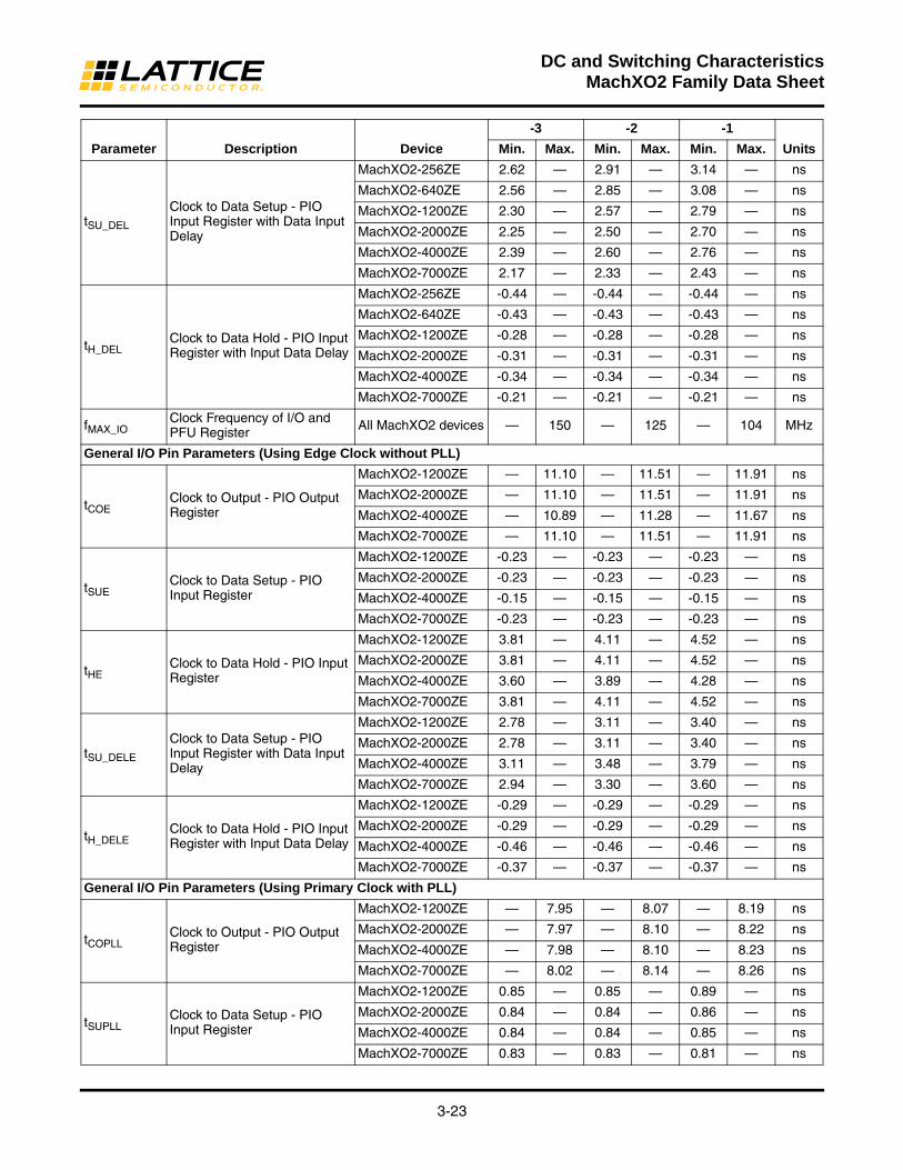
3-23
DC and Switching CharacteristicsMachXO2 Family Data Sheet
tSU_DEL
Clock to Data Setup - PIO Input Register with Data Input Delay
MachXO2-256ZE 2.62 — 2.91 — 3.14 — ns
MachXO2-640ZE 2.56 — 2.85 — 3.08 — ns
MachXO2-1200ZE 2.30 — 2.57 — 2.79 — ns
MachXO2-2000ZE 2.25 — 2.50 — 2.70 — ns
MachXO2-4000ZE 2.39 — 2.60 — 2.76 — ns
MachXO2-7000ZE 2.17 — 2.33 — 2.43 — ns
tH_DELClock to Data Hold - PIO Input Register with Input Data Delay
MachXO2-256ZE -0.44 — -0.44 — -0.44 — ns
MachXO2-640ZE -0.43 — -0.43 — -0.43 — ns
MachXO2-1200ZE -0.28 — -0.28 — -0.28 — ns
MachXO2-2000ZE -0.31 — -0.31 — -0.31 — ns
MachXO2-4000ZE -0.34 — -0.34 — -0.34 — ns
MachXO2-7000ZE -0.21 — -0.21 — -0.21 — ns
fMAX_IOClock Frequency of I/O and PFU Register All MachXO2 devices — 150 — 125 — 104 MHz
General I/O Pin Parameters (Using Edge Clock without PLL)
tCOEClock to Output - PIO Output Register
MachXO2-1200ZE — 11.10 — 11.51 — 11.91 ns
MachXO2-2000ZE — 11.10 — 11.51 — 11.91 ns
MachXO2-4000ZE — 10.89 — 11.28 — 11.67 ns
MachXO2-7000ZE — 11.10 — 11.51 — 11.91 ns
tSUEClock to Data Setup - PIO Input Register
MachXO2-1200ZE -0.23 — -0.23 — -0.23 — ns
MachXO2-2000ZE -0.23 — -0.23 — -0.23 — ns
MachXO2-4000ZE -0.15 — -0.15 — -0.15 — ns
MachXO2-7000ZE -0.23 — -0.23 — -0.23 — ns
tHEClock to Data Hold - PIO Input Register
MachXO2-1200ZE 3.81 — 4.11 — 4.52 — ns
MachXO2-2000ZE 3.81 — 4.11 — 4.52 — ns
MachXO2-4000ZE 3.60 — 3.89 — 4.28 — ns
MachXO2-7000ZE 3.81 — 4.11 — 4.52 — ns
tSU_DELE
Clock to Data Setup - PIO Input Register with Data Input Delay
MachXO2-1200ZE 2.78 — 3.11 — 3.40 — ns
MachXO2-2000ZE 2.78 — 3.11 — 3.40 — ns
MachXO2-4000ZE 3.11 — 3.48 — 3.79 — ns
MachXO2-7000ZE 2.94 — 3.30 — 3.60 — ns
tH_DELEClock to Data Hold - PIO Input Register with Input Data Delay
MachXO2-1200ZE -0.29 — -0.29 — -0.29 — ns
MachXO2-2000ZE -0.29 — -0.29 — -0.29 — ns
MachXO2-4000ZE -0.46 — -0.46 — -0.46 — ns
MachXO2-7000ZE -0.37 — -0.37 — -0.37 — ns
General I/O Pin Parameters (Using Primary Clock with PLL)
tCOPLLClock to Output - PIO Output Register
MachXO2-1200ZE — 7.95 — 8.07 — 8.19 ns
MachXO2-2000ZE — 7.97 — 8.10 — 8.22 ns
MachXO2-4000ZE — 7.98 — 8.10 — 8.23 ns
MachXO2-7000ZE — 8.02 — 8.14 — 8.26 ns
tSUPLLClock to Data Setup - PIO Input Register
MachXO2-1200ZE 0.85 — 0.85 — 0.89 — ns
MachXO2-2000ZE 0.84 — 0.84 — 0.86 — ns
MachXO2-4000ZE 0.84 — 0.84 — 0.85 — ns
MachXO2-7000ZE 0.83 — 0.83 — 0.81 — ns
Parameter Description Device
-3 -2 -1
UnitsMin. Max. Min. Max. Min. Max.
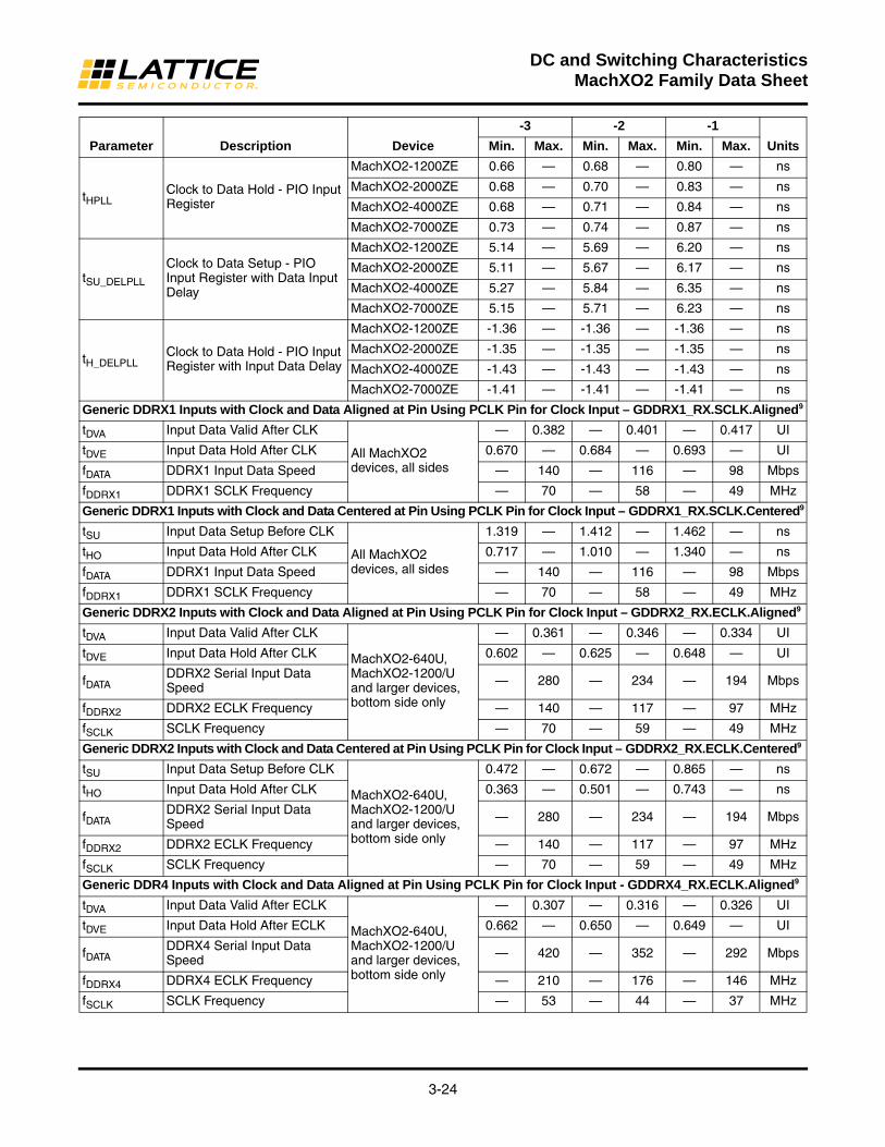
3-24
DC and Switching CharacteristicsMachXO2 Family Data Sheet
tHPLLClock to Data Hold - PIO Input Register
MachXO2-1200ZE 0.66 — 0.68 — 0.80 — ns
MachXO2-2000ZE 0.68 — 0.70 — 0.83 — ns
MachXO2-4000ZE 0.68 — 0.71 — 0.84 — ns
MachXO2-7000ZE 0.73 — 0.74 — 0.87 — ns
tSU_DELPLL
Clock to Data Setup - PIO Input Register with Data Input Delay
MachXO2-1200ZE 5.14 — 5.69 — 6.20 — ns
MachXO2-2000ZE 5.11 — 5.67 — 6.17 — ns
MachXO2-4000ZE 5.27 — 5.84 — 6.35 — ns
MachXO2-7000ZE 5.15 — 5.71 — 6.23 — ns
tH_DELPLLClock to Data Hold - PIO Input Register with Input Data Delay
MachXO2-1200ZE -1.36 — -1.36 — -1.36 — ns
MachXO2-2000ZE -1.35 — -1.35 — -1.35 — ns
MachXO2-4000ZE -1.43 — -1.43 — -1.43 — ns
MachXO2-7000ZE -1.41 — -1.41 — -1.41 — ns
Generic DDRX1 Inputs with Clock and Data Aligned at Pin Using PCLK Pin for Clock Input – GDDRX1_RX.SCLK.Aligned9
tDVA Input Data Valid After CLK
All MachXO2 devices, all sides
— 0.382 — 0.401 — 0.417 UI
tDVE Input Data Hold After CLK 0.670 — 0.684 — 0.693 — UI
fDATA DDRX1 Input Data Speed — 140 — 116 — 98 Mbps
fDDRX1 DDRX1 SCLK Frequency — 70 — 58 — 49 MHz
Generic DDRX1 Inputs with Clock and Data Centered at Pin Using PCLK Pin for Clock Input – GDDRX1_RX.SCLK.Centered9
tSU Input Data Setup Before CLK
All MachXO2 devices, all sides
1.319 — 1.412 — 1.462 — ns
tHO Input Data Hold After CLK 0.717 — 1.010 — 1.340 — ns
fDATA DDRX1 Input Data Speed — 140 — 116 — 98 Mbps
fDDRX1 DDRX1 SCLK Frequency — 70 — 58 — 49 MHz
Generic DDRX2 Inputs with Clock and Data Aligned at Pin Using PCLK Pin for Clock Input – GDDRX2_RX.ECLK.Aligned9
tDVA Input Data Valid After CLK
MachXO2-640U, MachXO2-1200/U and larger devices, bottom side only
— 0.361 — 0.346 — 0.334 UI
tDVE Input Data Hold After CLK 0.602 — 0.625 — 0.648 — UI
fDATADDRX2 Serial Input Data Speed — 280 — 234 — 194 Mbps
fDDRX2 DDRX2 ECLK Frequency — 140 — 117 — 97 MHz
fSCLK SCLK Frequency — 70 — 59 — 49 MHz
Generic DDRX2 Inputs with Clock and Data Centered at Pin Using PCLK Pin for Clock Input – GDDRX2_RX.ECLK.Centered9
tSU Input Data Setup Before CLK
MachXO2-640U, MachXO2-1200/U and larger devices, bottom side only
0.472 — 0.672 — 0.865 — ns
tHO Input Data Hold After CLK 0.363 — 0.501 — 0.743 — ns
fDATADDRX2 Serial Input Data Speed — 280 — 234 — 194 Mbps
fDDRX2 DDRX2 ECLK Frequency — 140 — 117 — 97 MHz
fSCLK SCLK Frequency — 70 — 59 — 49 MHz
Generic DDR4 Inputs with Clock and Data Aligned at Pin Using PCLK Pin for Clock Input - GDDRX4_RX.ECLK.Aligned9
tDVA Input Data Valid After ECLK
MachXO2-640U, MachXO2-1200/U and larger devices, bottom side only
— 0.307 — 0.316 — 0.326 UI
tDVE Input Data Hold After ECLK 0.662 — 0.650 — 0.649 — UI
fDATADDRX4 Serial Input Data Speed — 420 — 352 — 292 Mbps
fDDRX4 DDRX4 ECLK Frequency — 210 — 176 — 146 MHz
fSCLK SCLK Frequency — 53 — 44 — 37 MHz
Parameter Description Device
-3 -2 -1
UnitsMin. Max. Min. Max. Min. Max.

3-25
DC and Switching CharacteristicsMachXO2 Family Data Sheet
Generic DDR4 Inputs with Clock and Data Centered at Pin Using PCLK Pin for Clock Input – GDDRX4_RX.ECLK.Centered9
tSU Input Data Setup Before ECLK
MachXO2-640U, MachXO2-1200/U and larger devices, bottom side only
0.434 — 0.535 — 0.630 — ns
tHO Input Data Hold After ECLK 0.385 — 0.395 — 0.463 — ns
fDATADDRX4 Serial Input Data Speed — 420 — 352 — 292 Mbps
fDDRX4 DDRX4 ECLK Frequency — 210 — 176 — 146 MHz
fSCLK SCLK Frequency — 53 — 44 — 37 MHz
7:1 LVDS Inputs – GDDR71_RX.ECLK.7.19
tDVA Input Data Valid After ECLK
MachXO2-640U, MachXO2-1200/U and larger devices, bottom side only
— 0.307 — 0.316 — 0.326 UI
tDVE Input Data Hold After ECLK 0.662 — 0.650 — 0.649 — UI
fDATADDR71 Serial Input Data Speed — 420 — 352 — 292 Mbps
fDDR71 DDR71 ECLK Frequency — 210 — 176 — 146 MHz
fCLKIN
7:1 Input Clock Frequency (SCLK) (minimum limited by PLL)
— 60 — 50 — 42 MHz
Generic DDR Outputs with Clock and Data Aligned at Pin Using PCLK Pin for Clock Input – GDDRX1_TX.SCLK.Aligned9
tDIAOutput Data Invalid After CLK Output
All MachXO2 devices, all sides
— 0.850 — 0.910 — 0.970 ns
tDIBOutput Data Invalid Before CLK Output — 0.850 — 0.910 — 0.970 ns
fDATA DDRX1 Output Data Speed — 140 — 116 — 98 Mbps
fDDRX1 DDRX1 SCLK frequency — 70 — 58 — 49 MHz
Generic DDR Outputs with Clock and Data Centered at Pin Using PCLK Pin for Clock Input – GDDRX1_TX.SCLK.Centered9
tDVBOutput Data Valid Before CLK Output
All MachXO2 devices, all sides
2.720 — 3.380 — 4.140 — ns
tDVAOutput Data Valid After CLK Output 2.720 — 3.380 — 4.140 — ns
fDATA DDRX1 Output Data Speed — 140 — 116 — 98 Mbps
fDDRX1DDRX1 SCLK Frequency(minimum limited by PLL) — 70 — 58 — 49 MHz
Generic DDRX2 Outputs with Clock and Data Aligned at Pin Using PCLK Pin for Clock Input – GDDRX2_TX.ECLK.Aligned9
tDIAOutput Data Invalid After CLK Output
MachXO2-640U, MachXO2-1200/U and larger devices, top side only
— 0.270 — 0.300 — 0.330 ns
tDIBOutput Data Invalid Before CLK Output — 0.270 — 0.300 — 0.330 ns
fDATADDRX2 Serial Output Data Speed — 280 — 234 — 194 Mbps
fDDRX2 DDRX2 ECLK frequency — 140 — 117 — 97 MHz
fSCLK SCLK Frequency — 70 — 59 — 49 MHz
Parameter Description Device
-3 -2 -1
UnitsMin. Max. Min. Max. Min. Max.
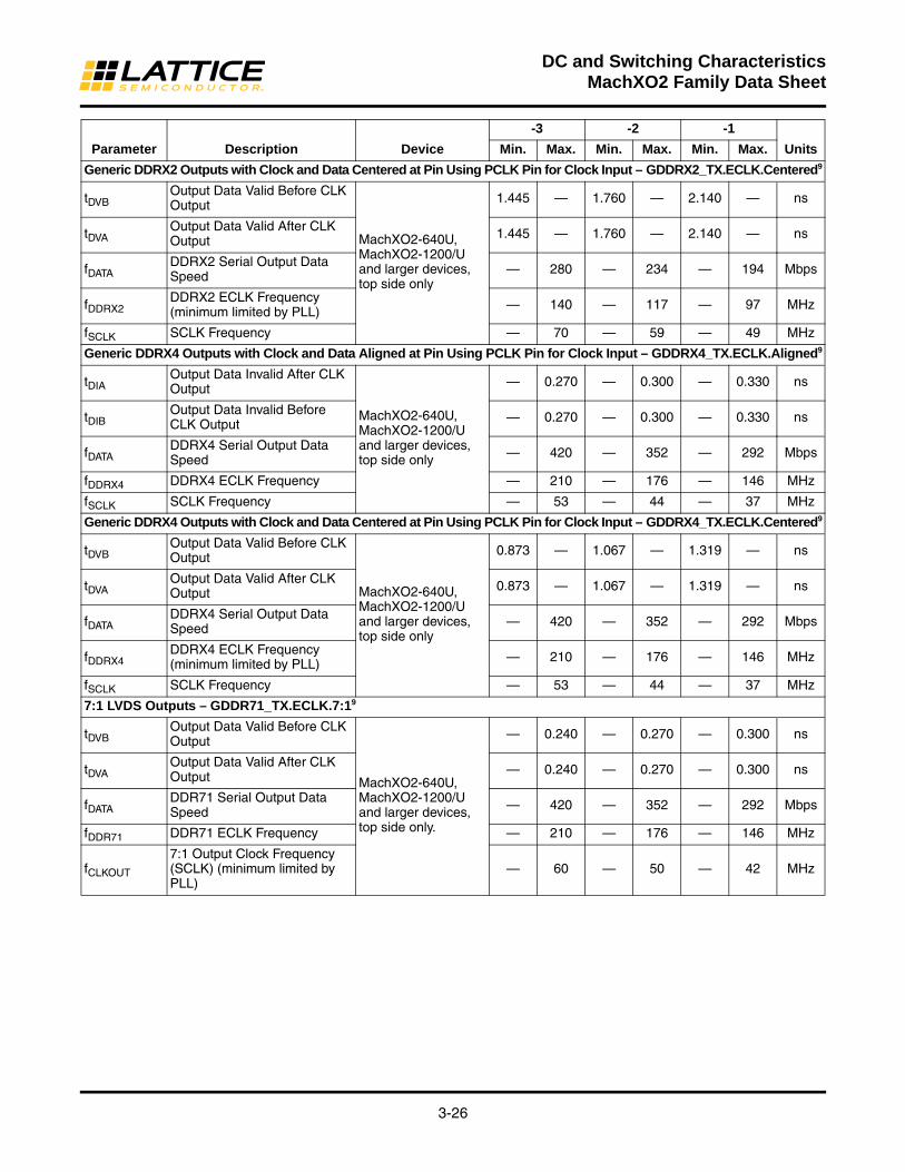
3-26
DC and Switching CharacteristicsMachXO2 Family Data Sheet
Generic DDRX2 Outputs with Clock and Data Centered at Pin Using PCLK Pin for Clock Input – GDDRX2_TX.ECLK.Centered9
tDVBOutput Data Valid Before CLK Output
MachXO2-640U, MachXO2-1200/U and larger devices, top side only
1.445 — 1.760 — 2.140 — ns
tDVAOutput Data Valid After CLK Output 1.445 — 1.760 — 2.140 — ns
fDATADDRX2 Serial Output Data Speed — 280 — 234 — 194 Mbps
fDDRX2DDRX2 ECLK Frequency(minimum limited by PLL) — 140 — 117 — 97 MHz
fSCLK SCLK Frequency — 70 — 59 — 49 MHz
Generic DDRX4 Outputs with Clock and Data Aligned at Pin Using PCLK Pin for Clock Input – GDDRX4_TX.ECLK.Aligned9
tDIAOutput Data Invalid After CLK Output
MachXO2-640U, MachXO2-1200/U and larger devices, top side only
— 0.270 — 0.300 — 0.330 ns
tDIBOutput Data Invalid Before CLK Output — 0.270 — 0.300 — 0.330 ns
fDATADDRX4 Serial Output Data Speed — 420 — 352 — 292 Mbps
fDDRX4 DDRX4 ECLK Frequency — 210 — 176 — 146 MHz
fSCLK SCLK Frequency — 53 — 44 — 37 MHz
Generic DDRX4 Outputs with Clock and Data Centered at Pin Using PCLK Pin for Clock Input – GDDRX4_TX.ECLK.Centered9
tDVBOutput Data Valid Before CLK Output
MachXO2-640U, MachXO2-1200/U and larger devices, top side only
0.873 — 1.067 — 1.319 — ns
tDVAOutput Data Valid After CLK Output 0.873 — 1.067 — 1.319 — ns
fDATADDRX4 Serial Output Data Speed — 420 — 352 — 292 Mbps
fDDRX4DDRX4 ECLK Frequency (minimum limited by PLL) — 210 — 176 — 146 MHz
fSCLK SCLK Frequency — 53 — 44 — 37 MHz
7:1 LVDS Outputs – GDDR71_TX.ECLK.7:19
tDVBOutput Data Valid Before CLK Output
MachXO2-640U, MachXO2-1200/U and larger devices, top side only.
— 0.240 — 0.270 — 0.300 ns
tDVAOutput Data Valid After CLK Output — 0.240 — 0.270 — 0.300 ns
fDATADDR71 Serial Output Data Speed — 420 — 352 — 292 Mbps
fDDR71 DDR71 ECLK Frequency — 210 — 176 — 146 MHz
fCLKOUT
7:1 Output Clock Frequency (SCLK) (minimum limited by PLL)
— 60 — 50 — 42 MHz
Parameter Description Device
-3 -2 -1
UnitsMin. Max. Min. Max. Min. Max.

3-27
DC and Switching CharacteristicsMachXO2 Family Data Sheet
LPDDR9
tDVADQInput Data Valid After DQS Input
MachXO2-1200/U and larger devices, right side only.
— 0.461 — 0.472 — 0.483 UI
tDVEDQInput Data Hold After DQS Input 0.665 — 0.652 — 0.632 — UI
tDQVBSOutput Data Invalid Before DQS Output 0.030 — 0.028 — 0.024 — UI
tDQVASOutput Data Invalid After DQS Output 0.030 — 0.028 — 0.024 — UI
fDATAMEM LPDDR Serial Data Speed — 120 — 110 — 96 Mbps
fSCLK SCLK Frequency — 60 — 55 — 48 MHz
fLPDDR LPDDR Data Transfer Rate 0 120 0 110 0 96 Mbps
DDR9
tDVADQInput Data Valid After DQS Input
MachXO2-1200/U and larger devices, right side only.
— 0.450 — 0.466 — 0.479 UI
tDVEDQInput Data Hold After DQS Input 0.693 — 0.660 — 0.635 — UI
tDQVBSOutput Data Invalid Before DQS Output 0.035 — 0.029 — 0.025 — UI
tDQVASOutput Data Invalid After DQS Output 0.035 — 0.029 — 0.025 — UI
fDATA MEM DDR Serial Data Speed — 140 — 116 — 98 Mbps
fSCLK SCLK Frequency — 70 — 58 — 49 MHz
fMEM_DDR MEM DDR Data Transfer Rate N/A 140 N/A 116 N/A 98 Mbps
DDR29
tDVADQInput Data Valid After DQS Input
MachXO2-1200/U and larger devices, right side only.
— 0.447 — 0.464 — 0.477 UI
tDVEDQInput Data Hold After DQS Input 0.690 — 0.657 — 0.633 — UI
tDQVBSOutput Data Invalid Before DQS Output 0.035 — 0.029 — 0.025 — UI
tDQVASOutput Data Invalid After DQS Output 0.035 — 0.029 — 0.025 — UI
fDATA MEM DDR Serial Data Speed — 140 — 116 — 98 Mbps
fSCLK SCLK Frequency — 70 — 58 — 49 MHz
fMEM_DDR2MEM DDR2 Data Transfer Rate N/A 140 N/A 116 N/A 98 Mbps
1. Exact performance may vary with device and design implementation. Commercial timing numbers are shown at 85°C and 1.14V. Other operating conditions, including industrial, can be extracted from the Diamond software.
2. General I/O timing numbers based on LVCMOS 2.5, 8mA, 0pf load.3. Generic DDR timing numbers based on LVDS I/O (for input, output, and clock ports).4. DDR timing numbers based on SSTL25. DDR2 timing numbers based on SSTL18. LPDDR timing numbers based in LVCMOS18.5. 7:1 LVDS (GDDR71) uses the LVDS I/O standard (for input, output, and clock ports).6. For Generic DDRX1 mode tSU = tHO = (tDVE - tDVA - 0.03ns)/2.7. The tSU_DEL and tH_DEL values use the SCLK_ZERHOLD default step size. Each step is 167ps (-3), 182ps (-2), 195ps (-1).8. This number for general purpose usage. Duty cycle tolerance is +/-10%.9. Duty cycle is +/- 5% for system usage.10. The above timing numbers are generated using the Diamond design tool. Exact performance may vary with the device selected.
Parameter Description Device
-3 -2 -1
UnitsMin. Max. Min. Max. Min. Max.

3-28
DC and Switching CharacteristicsMachXO2 Family Data Sheet
Figure 3-5. Receiver RX.CLK.Aligned and MEM DDR Input Waveforms
Figure 3-6. Receiver RX.CLK.Centered Waveforms
Figure 3-7. Transmitter TX.CLK.Aligned Waveforms
Figure 3-8. Transmitter TX.CLK.Centered and MEM DDR Output Waveforms
tDVA or tDVADQ
tDVE or tDVEDQ
RX.Aligned
RX CLK Inputor DQS Input
RX Data Inputor DQ Input
tHO tHOtSUtSU
RX.Centered
RX CLK Input
RX Data Input
TX CLK Output
tDIA
TX Data Output
tDIB
TX.Aligned
tDIAtDIB
TX CLK Outputor DQS Output
tDVA or tDQVAS
TX Data Outputor DQ Output
tDVB ortDQVBS
TX.Centered
tDVA or tDQVAS
tDVB ortDQVBS
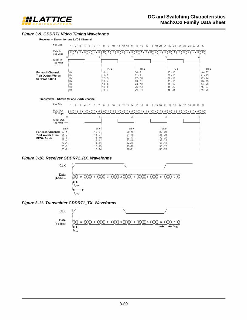
3-29
DC and Switching CharacteristicsMachXO2 Family Data Sheet
Figure 3-9. GDDR71 Video Timing Waveforms
Figure 3-10. Receiver GDDR71_RX. Waveforms
Figure 3-11. Transmitter GDDR71_TX. Waveforms
756 Mbps
Data Out756 Mbps
Clock Out125 MHz
Clock In125 MHz
tDVA
tDVE
0 1 2 3 4 5 6 0
tDIA
tDIB
0 1 2 3 4 5 6 0
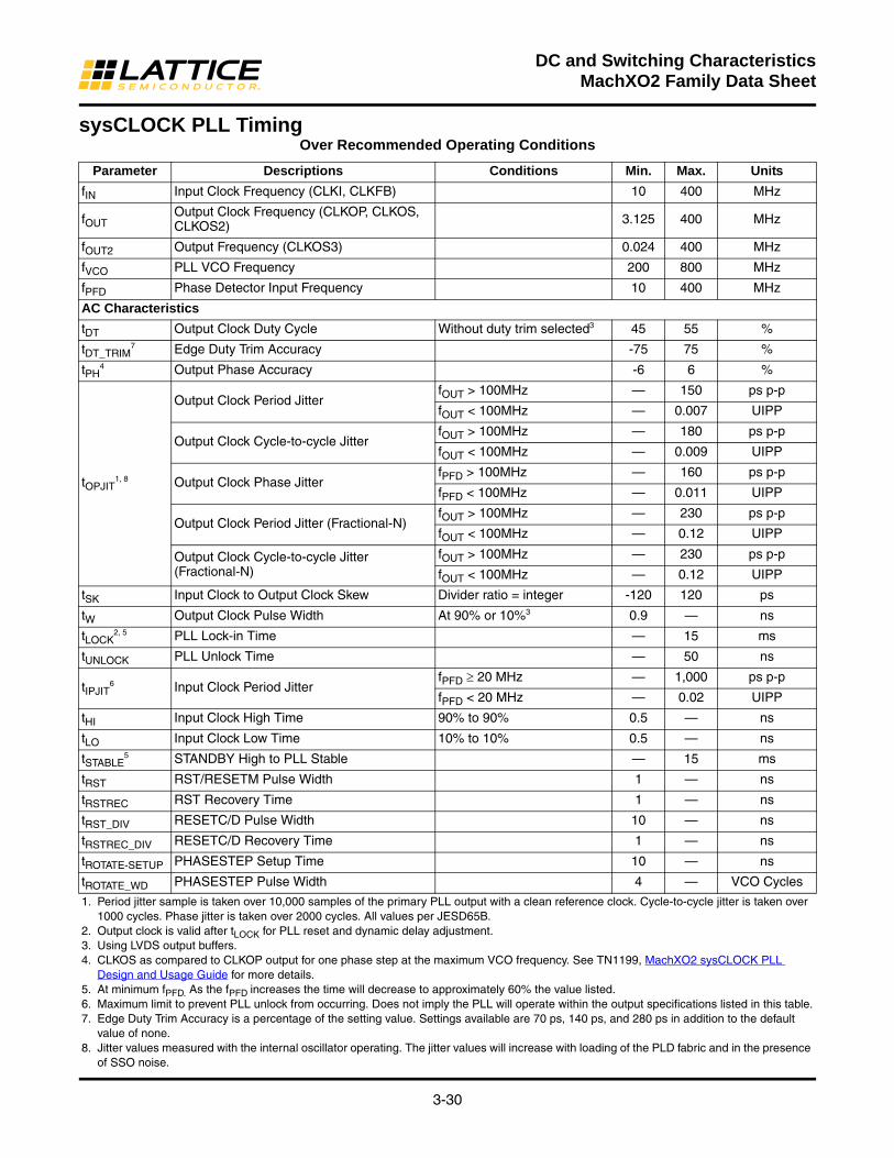
3-30
DC and Switching CharacteristicsMachXO2 Family Data Sheet
sysCLOCK PLL TimingOver Recommended Operating Conditions
Parameter Descriptions Conditions Min. Max. Units
fIN Input Clock Frequency (CLKI, CLKFB) 10 400 MHz
fOUTOutput Clock Frequency (CLKOP, CLKOS, CLKOS2) 3.125 400 MHz
fOUT2 Output Frequency (CLKOS3) 0.024 400 MHz
fVCO PLL VCO Frequency 200 800 MHz
fPFD Phase Detector Input Frequency 10 400 MHz
AC Characteristics
tDT Output Clock Duty Cycle Without duty trim selected3 45 55 %
tDT_TRIM7 Edge Duty Trim Accuracy -75 75 %
tPH4 Output Phase Accuracy -6 6 %
tOPJIT1, 8
Output Clock Period JitterfOUT > 100MHz — 150 ps p-p
fOUT < 100MHz — 0.007 UIPP
Output Clock Cycle-to-cycle JitterfOUT > 100MHz — 180 ps p-p
fOUT < 100MHz — 0.009 UIPP
Output Clock Phase JitterfPFD > 100MHz — 160 ps p-p
fPFD < 100MHz — 0.011 UIPP
Output Clock Period Jitter (Fractional-N)fOUT > 100MHz — 230 ps p-p
fOUT < 100MHz — 0.12 UIPP
Output Clock Cycle-to-cycle Jitter (Fractional-N)
fOUT > 100MHz — 230 ps p-p
fOUT < 100MHz — 0.12 UIPP
tSK Input Clock to Output Clock Skew Divider ratio = integer -120 120 ps
tW Output Clock Pulse Width At 90% or 10%3 0.9 — ns
tLOCK2, 5 PLL Lock-in Time — 15 ms
tUNLOCK PLL Unlock Time — 50 ns
tIPJIT6 Input Clock Period Jitter
fPFD 20 MHz — 1,000 ps p-p
fPFD < 20 MHz — 0.02 UIPP
tHI Input Clock High Time 90% to 90% 0.5 — ns
tLO Input Clock Low Time 10% to 10% 0.5 — ns
tSTABLE5 STANDBY High to PLL Stable — 15 ms
tRST RST/RESETM Pulse Width 1 — ns
tRSTREC RST Recovery Time 1 — ns
tRST_DIV RESETC/D Pulse Width 10 — ns
tRSTREC_DIV RESETC/D Recovery Time 1 — ns
tROTATE-SETUP PHASESTEP Setup Time 10 — ns
tROTATE_WD PHASESTEP Pulse Width 4 — VCO Cycles
1. Period jitter sample is taken over 10,000 samples of the primary PLL output with a clean reference clock. Cycle-to-cycle jitter is taken over 1000 cycles. Phase jitter is taken over 2000 cycles. All values per JESD65B.
2. Output clock is valid after tLOCK for PLL reset and dynamic delay adjustment.3. Using LVDS output buffers.4. CLKOS as compared to CLKOP output for one phase step at the maximum VCO frequency. See TN1199, MachXO2 sysCLOCK PLL
Design and Usage Guide for more details.5. At minimum fPFD. As the fPFD increases the time will decrease to approximately 60% the value listed.6. Maximum limit to prevent PLL unlock from occurring. Does not imply the PLL will operate within the output specifications listed in this table.7. Edge Duty Trim Accuracy is a percentage of the setting value. Settings available are 70 ps, 140 ps, and 280 ps in addition to the default
value of none.8. Jitter values measured with the internal oscillator operating. The jitter values will increase with loading of the PLD fabric and in the presence
of SSO noise.

3-31
DC and Switching CharacteristicsMachXO2 Family Data Sheet
MachXO2 Oscillator Output Frequency
MachXO2 Standby Mode Timing – ZE Devices
MachXO2 Standby Mode Timing – HC/HE Devices
Symbol Parameter Min. Typ. Max Units
fMAX
Oscillator Output Frequency (Commercial Grade Devices, 0 to 85°C) 125.685 133 140.315 MHz
Oscillator Output Frequency (Industrial Grade Devices, -40 to 100°C) 124.355 133 141.645 MHz
tDT Output Clock Duty Cycle 43 50 57 %
tOPJIT1 Output Clock Period Jitter 0.01 0.012 0.02 UIPP
tSTABLE STDBY Low to Oscillator Stable 0.01 0.05 0.1 µs
1. Output Clock Period Jitter specified at 133MHz. The values for lower frequencies will be smaller UIPP. The typical value for 133MHz is 95ps and for 2.08MHz the typical value is 1.54ns.
Symbol Parameter Device Min. Typ. Max Units
tPWRDN USERSTDBY High to Stop All — — 13 ns
tPWRUP USERSTDBY Low to Power Up
LCMXO2-256 — µs
LCMXO2-640 — µs
LCMXO2-1200 20 — 50 µs
LCMXO2-2000 — µs
LCMXO2-4000 — µs
LCMXO2-7000 — µs
tWSTDBY USERSTDBY Pulse Width All 19 — — ns
tBNDGAPSTBL USERSTDBY High to Bandgap Stable All — — 15 ns
Symbol Parameter Device Min. Typ. Max Units
tPWRDN USERSTDBY High to Stop All — — 9 ns
tPWRUP USERSTDBY Low to Power Up
LCMXO2-256 — µs
LCMXO2-640 — µs
LCMXO2-640U — µs
LCMXO2-1200 20 — 50 µs
LCMXO2-1200U — µs
LCMXO2-2000 — µs
LCMXO2-2000U — µs
LCMXO2-4000 — µs
LCMXO2-7000 — µs
tWSTDBY USERSTDBY Pulse Width All 18 — — ns
USERSTDBY
tPWRUP
USERSTDBY Mode
tPWRDN
tWSTDBY
BG, POR

3-32
DC and Switching CharacteristicsMachXO2 Family Data Sheet
Flash Download Time1, 2
JTAG Port Timing Specifications
Symbol Parameter Device Typ. Units
tREFRESH POR to Device I/O Active
LCMXO2-256 0.6 ms
LCMXO2-640 1.0 ms
LCMXO2-640U 1.9 ms
LCMXO2-1200 1.9 ms
LCMXO2-1200U 1.4 ms
LCMXO2-2000 1.4 ms
LCMXO2-2000U 2.4 ms
LCMXO2-4000 2.4 ms
LCMXO2-7000 3.8 ms
1. Assumes sysMEM EBR initialized to an all zero pattern if they are used.2. The Flash download time is measured starting from the maximum voltage of POR trip point.
Symbol Parameter Min. Max. Units
fMAX TCK clock frequency — 25 MHz
tBTCPH TCK [BSCAN] clock pulse width high 20 — ns
tBTCPL TCK [BSCAN] clock pulse width low 20 — ns
tBTS TCK [BSCAN] setup time 10 — ns
tBTH TCK [BSCAN] hold time 8 — ns
tBTCO TAP controller falling edge of clock to valid output — 10 ns
tBTCODIS TAP controller falling edge of clock to valid disable — 10 ns
tBTCOEN TAP controller falling edge of clock to valid enable — 10 ns
tBTCRS BSCAN test capture register setup time 8 — ns
tBTCRH BSCAN test capture register hold time 20 — ns
tBUTCO BSCAN test update register, falling edge of clock to valid output — 25 ns
tBTUODIS BSCAN test update register, falling edge of clock to valid disable — 25 ns
tBTUPOEN BSCAN test update register, falling edge of clock to valid enable — 25 ns
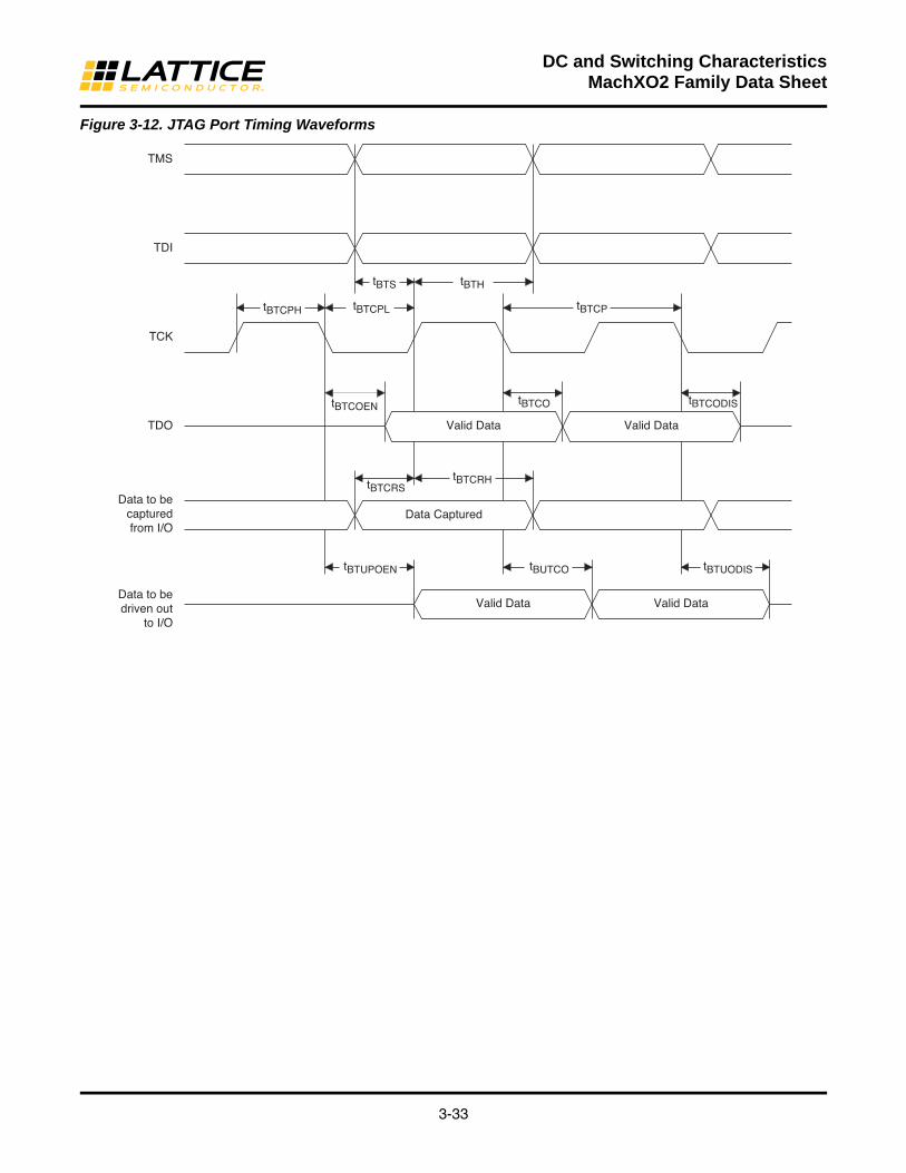
3-33
DC and Switching CharacteristicsMachXO2 Family Data Sheet
Figure 3-12. JTAG Port Timing Waveforms
TMS
TDI
TCK
TDO
Data to becapturedfrom I/O
Data to bedriven out
to I/O
ataD dilaVataD dilaV
ataD dilaVataD dilaV
Data Captured
tBTCPH tBTCPL
tBTCOEN
tBTCRS
tBTUPOEN tBUTCO tBTUODIS
tBTCRH
tBTCO tBTCODIS
tBTS tBTH
tBTCP
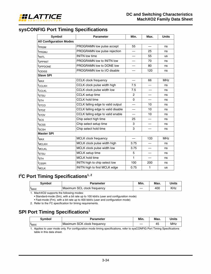
3-34
DC and Switching CharacteristicsMachXO2 Family Data Sheet
sysCONFIG Port Timing Specifications
I2C Port Timing Specifications1, 2
SPI Port Timing Specifications1
Symbol Parameter Min. Max. Units
All Configuration Modes
tPRGM PROGRAMN low pulse accept 55 — ns
tPRGMJ PROGRAMN low pulse rejection — 25 ns
tINITL INITN low time — 55 us
tDPPINIT PROGRAMN low to INITN low — 70 ns
tDPPDONE PROGRAMN low to DONE low — 80 ns
tIODISS PROGRAMN low to I/O disable — 120 ns
Slave SPI
fMAX CCLK clock frequency — 66 MHz
tCCLKH CCLK clock pulse width high 7.5 — ns
tCCLKL CCLK clock pulse width low 7.5 — ns
tSTSU CCLK setup time 2 — ns
tSTH CCLK hold time 0 — ns
tSTCO CCLK falling edge to valid output — 10 ns
tSTOZ CCLK falling edge to valid disable — 10 ns
tSTOV CCLK falling edge to valid enable — 10 ns
tSCS Chip select high time 25 — ns
tSCSS Chip select setup time 3 — ns
tSCSH Chip select hold time 3 — ns
Master SPI
fMAX MCLK clock frequency — 133 MHz
tMCLKH MCLK clock pulse width high 3.75 — ns
tMCLKL MCLK clock pulse width low 3.75 — ns
tSTSU MCLK setup time 5 — ns
tSTH MCLK hold time 1 — ns
tCSSPI INITN high to chip select low 100 200 ns
tMCLK INITN high to first MCLK edge 0.75 1 us
Symbol Parameter Min. Max. Units
fMAX Maximum SCL clock frequency — 400 KHz
1. MachXO2 supports the following modes:• Standard-mode (Sm), with a bit rate up to 100 kbit/s (user and configuration mode)• Fast-mode (Fm), with a bit rate up to 400 kbit/s (user and configuration mode)
2. Refer to the I2C specification for timing requirements.
Symbol Parameter Min. Max. Units
fMAX Maximum SCK clock frequency — 45 MHz
1. Applies to user mode only. For configuration mode timing specifications, refer to sysCONFIG Port Timing Specifications table in this data sheet.

3-35
DC and Switching CharacteristicsMachXO2 Family Data Sheet
Switching Test ConditionsFigure 3-13 shows the output test load used for AC testing. The specific values for resistance, capacitance, volt-age, and other test conditions are shown in Table 3-5.
Figure 3-13. Output Test Load, LVTTL and LVCMOS Standards
Table 3-5. Test Fixture Required Components, Non-Terminated Interfaces
Note: Output test conditions for all other interfaces are determined by the respective standards.
Test Condition R1 CL Timing Ref. VT
LVTTL and LVCMOS settings (L -> H, H -> L) 0pF
LVTTL, LVCMOS 3.3 = 1.5V —
LVCMOS 2.5 = VCCIO/2 —
LVCMOS 1.8 = VCCIO/2 —
LVCMOS 1.5 = VCCIO/2 —
LVCMOS 1.2 = VCCIO/2 —
LVTTL and LVCMOS 3.3 (Z -> H)
188 0pF
1.5 VOL
LVTTL and LVCMOS 3.3 (Z -> L) 1.5 VOH
Other LVCMOS (Z -> H) VCCIO/2 VOL
Other LVCMOS (Z -> L) VCCIO/2 VOH
LVTTL + LVCMOS (H -> Z) VOH - 0.15 VOL
LVTTL + LVCMOS (L -> Z) VOL - 0.15 VOH
DUT
V T
R1
CL
Test Poi n t

www.latticesemi.com 4-1 DS1035 Pinout Information_01.6
March 2012 Data Sheet DS1035
© 2012 Lattice Semiconductor Corp. All Lattice trademarks, registered trademarks, patents, and disclaimers are as listed at www.latticesemi.com/legal. All other brand or product names are trademarks or registered trademarks of their respective holders. The specifications and information herein are subject to change without notice.
Signal DescriptionsSignal Name I/O Descriptions
General Purpose
P[Edge] [Row/Column Number]_[A/B/C/D] I/O
[Edge] indicates the edge of the device on which the pad is located. Valid edge designations are L (Left), B (Bottom), R (Right), T (Top).
[Row/Column Number] indicates the PFU row or the column of the device on which the PIO Group exists. When Edge is T (Top) or (Bottom), only need to specify Row Number. When Edge is L (Left) or R (Right), only need to specify Column Number.
[A/B/C/D] indicates the PIO within the group to which the pad is connected.
Some of these user-programmable pins are shared with special function pins. When not used as special function pins, these pins can be programmed as I/Os for user logic.
During configuration of the user-programmable I/Os, the user has an option to tri-state the I/Os and enable an internal pull-up, pull-down or buskeeper resistor. This option also applies to unused pins (or those not bonded to a package pin). The default during configuration is for user-programmable I/Os to be tri-stated with an internal pull-down resistor enabled. When the device is erased, I/Os will be tri-stated with an internal pull-down resistor enabled. Some pins, such as PROGRAMN and JTAG pins, default to tri-stated I/Os with pull-up resistors enabled when the device is erased.
NC — No connect.
GND — GND – Ground. Dedicated pins. It is recommended that all GNDs are tied together.
VCC — VCC – The power supply pins for core logic. Dedicated pins. It is recommended that all VCCs are tied to the same supply.
VCCIOx — VCCIO – The power supply pins for I/O Bank x. Dedicated pins. It is recommended that all VCCIOs located in the same bank are tied to the same supply.
PLL and Clock Functions (Used as user-programmable I/O pins when not used for PLL or clock pins)
[LOC]_GPLL[T, C]_IN — Reference Clock (PLL) input pads: [LOC] indicates location. Valid designations are L (Left PLL) and R (Right PLL). T = true and C = complement.
[LOC]_GPLL[T, C]_FB — Optional Feedback (PLL) input pads: [LOC] indicates location. Valid designations are L (Left PLL) and R (Right PLL). T = true and C = complement.
PCLK [n]_[2:0] — Primary Clock pads. One to three clock pads per side.
Test and Programming (Dual function pins used for test access port and during sysCONFIG™)
TMS I Test Mode Select input pin, used to control the 1149.1 state machine.
TCK I Test Clock input pin, used to clock the 1149.1 state machine.
TDI I Test Data input pin, used to load data into the device using an 1149.1 state machine.
TDO O Output pin – Test Data output pin used to shift data out of the device using 1149.1.
JTAGENB I
Optionally controls behavior of TDI, TDO, TMS, TCK. If the device is configured to use the JTAG pins (TDI, TDO, TMS, TCK) as general purpose I/O, then:
If JTAGENB is low: TDI, TDO, TMS and TCK can function a general purpose I/O.
If JTAGENB is high: TDI, TDO, TMS and TCK function as JTAG pins.
For more details, refer to TN1204, MachXO2 Programming and Configuration Usage Guide.
Configuration (Dual function pins used during sysCONFIG)
PROGRAMN I Initiates configuration sequence when asserted low. This pin always has an active pull-up.
INITN I/O Open Drain pin. Indicates the FPGA is ready to be configured. During configuration, a pull-up is enabled.
MachXO2 Family Data SheetPinout Information

4-2
Pinout InformationMachXO2 Family Data Sheet
DONE I/O Open Drain pin. Indicates that the configuration sequence is complete, and the start-up sequence is in progress.
MCLK/CCLK I/O Input Configuration Clock for configuring an FPGA in Slave SPI mode. Output Configuration Clock for configuring an FPGA in SPI and SPIm configuration modes.
SN I Slave SPI active low chip select input.
CSSPIN I/O Master SPI active low chip select output.
SI/SISPI I/O Slave SPI serial data input and master SPI serial data output.
SO/SPISO I/O Slave SPI serial data output and master SPI serial data input.
SCL I/O Slave I2C clock input and master I2C clock output.
SDA I/O Slave I2C data input and master I2C data output.
Signal Name I/O Descriptions
General Purpose

4-3
Pinout InformationMachXO2 Family Data Sheet
Pin Information SummaryMachXO2-256 MachXO2-640 MachXO2-640U
32 QFN1 64 ucBGA 100 TQFP 132 csBGA 100 TQFP 132 csBGA 144 TQFP
General Purpose I/O per Bank
Bank 0 9 10 14 14 19 20 28
Bank 1 2 12 14 14 20 20 26
Bank 2 9 11 14 14 20 20 28
Bank 3 2 12 14 14 20 20 26
Bank 4 0 0 0 0 0 0 0
Bank 5 0 0 0 0 0 0 0
Total General Purpose Single Ended I/O 22 45 56 56 79 80 108
Differential I/O per Bank
Bank 0 4 5 7 7 9 10 14
Bank 1 1 6 7 7 10 10 13
Bank 2 4 5 7 7 10 10 14
Bank 3 1 6 7 7 10 10 13
Bank 4 0 0 0 0 0 0 0
Bank 5 0 0 0 0 0 0 0
Total General Purpose Differential I/O 10 22 28 28 39 40 54
Dual Function I/O 22 27 29 29 29 29 33
High-speed Differential I/O
Bank 0 0 0 0 0 0 0 7
Gearboxes
Number of 7:1 or 8:1 Output Gearbox Available (Bank 0) 0 0 0 0 0 0 7
Number of 7:1 or 8:1 Input Gearbox Available (Bank 2) 0 0 0 0 0 0 7
DQS Groups
Bank 1 0 0 0 0 0 0 2
VCCIO Pins
Bank 0 2 2 2 2 2 2 3
Bank 1 1 2 2 2 2 2 3
Bank 2 2 2 2 2 2 2 3
Bank 3 1 2 2 2 2 2 3
Bank 4 0 0 0 0 0 0 0
Bank 5 0 0 0 0 0 0 0
VCC 2 2 2 2 2 2 4
GND 2 8 8 8 8 10 12
NC 0 1 26 58 3 32 8
Total Count of Bonded Pins 32 63 74 74 97 100 136
1. Lattice recommends soldering the central thermal pad onto the top PCB ground for improved thermal resistance.

4-4
Pinout InformationMachXO2 Family Data Sheet
MachXO2-1200 MachXO2-1200U
100 TQFP 132 csBGA 144 TQFP 25 WLCSP 256 ftBGA
General Purpose I/O per Bank
Bank 0 19 26 28 12 51
Bank 1 21 26 26 0 52
Bank 2 20 28 28 7 52
Bank 3 20 25 26 0 16
Bank 4 0 0 0 0 16
Bank 5 0 0 0 0 20
Total General Purpose Single Ended I/O 80 105 108 19 207
Differential I/O per Bank
Bank 0 9 13 14 5 25
Bank 1 10 13 13 0 26
Bank 2 10 14 14 2 26
Bank 3 10 12 13 0 8
Bank 4 0 0 0 0 8
Bank 5 0 0 0 0 10
Total General Purpose Differential I/O 39 52 54 7 103
Dual Function I/O 31 33 33 18 33
High-speed Differential I/O
Bank 0 4 7 7 0 14
Gearboxes
Number of 7:1 or 8:1 Output Gearbox Available (Bank 0) 4 7 7 0 14
Number of 7:1 or 8:1 Input Gearbox Available (Bank 2) 5 7 7 0 14
DQS Groups
Bank 1 1 2 2 0 2
VCCIO Pins
Bank 0 2 3 3 1 4
Bank 1 2 3 3 0 4
Bank 2 2 3 3 1 4
Bank 3 3 3 3 0 1
Bank 4 0 0 0 0 2
Bank 5 0 0 0 0 1
VCC 2 4 4 2 8
GND 8 10 12 2 24
NC 1 1 8 0 1
Total Count of Bonded Pins 99 131 136 25 255
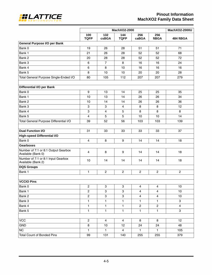
4-5
Pinout InformationMachXO2 Family Data Sheet
MachXO2-2000 MachXO2-2000U
100 TQFP
132 csBGA
144 TQFP
256 caBGA
256 ftBGA 484 ftBGA
General Purpose I/O per Bank
Bank 0 19 26 28 51 51 71
Bank 1 21 26 28 52 52 68
Bank 2 20 28 28 52 52 72
Bank 3 6 7 8 16 16 24
Bank 4 6 8 10 16 16 16
Bank 5 8 10 10 20 20 28
Total General Purpose Single-Ended I/O 80 105 112 207 207 279
Differential I/O per Bank
Bank 0 9 13 14 25 25 35
Bank 1 10 13 14 26 26 34
Bank 2 10 14 14 26 26 36
Bank 3 3 3 4 8 8 12
Bank 4 3 4 5 8 8 8
Bank 5 4 5 5 10 10 14
Total General Purpose Differential I/O 39 52 56 103 103 139
Dual Function I/O 31 33 33 33 33 37
High-speed Differential I/O
Bank 0 4 8 9 14 14 18
Gearboxes
Number of 7:1 or 8:1 Output Gearbox Available (Bank 0) 4 8 9 14 14 18
Number of 7:1 or 8:1 Input Gearbox Available (Bank 2) 10 14 14 14 14 18
DQS Groups
Bank 1 1 2 2 2 2 2
VCCIO Pins
Bank 0 2 3 3 4 4 10
Bank 1 2 3 3 4 4 10
Bank 2 2 3 3 4 4 10
Bank 3 1 1 1 1 1 3
Bank 4 1 1 1 2 2 4
Bank 5 1 1 1 1 1 3
VCC 2 4 4 8 8 12
GND 8 10 12 24 24 48
NC 1 1 4 1 1 105
Total Count of Bonded Pins 99 131 140 255 255 379
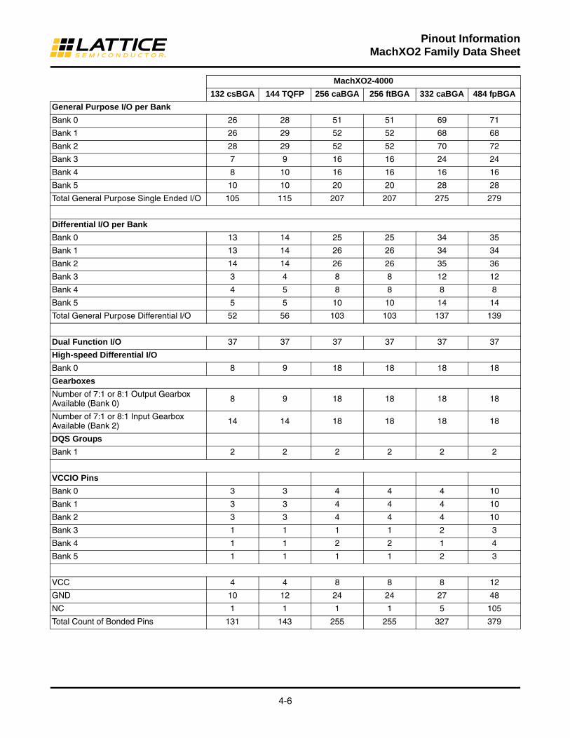
4-6
Pinout InformationMachXO2 Family Data Sheet
MachXO2-4000
132 csBGA 144 TQFP 256 caBGA 256 ftBGA 332 caBGA 484 fpBGA
General Purpose I/O per Bank
Bank 0 26 28 51 51 69 71
Bank 1 26 29 52 52 68 68
Bank 2 28 29 52 52 70 72
Bank 3 7 9 16 16 24 24
Bank 4 8 10 16 16 16 16
Bank 5 10 10 20 20 28 28
Total General Purpose Single Ended I/O 105 115 207 207 275 279
Differential I/O per Bank
Bank 0 13 14 25 25 34 35
Bank 1 13 14 26 26 34 34
Bank 2 14 14 26 26 35 36
Bank 3 3 4 8 8 12 12
Bank 4 4 5 8 8 8 8
Bank 5 5 5 10 10 14 14
Total General Purpose Differential I/O 52 56 103 103 137 139
Dual Function I/O 37 37 37 37 37 37
High-speed Differential I/O
Bank 0 8 9 18 18 18 18
Gearboxes
Number of 7:1 or 8:1 Output Gearbox Available (Bank 0) 8 9 18 18 18 18
Number of 7:1 or 8:1 Input Gearbox Available (Bank 2) 14 14 18 18 18 18
DQS Groups
Bank 1 2 2 2 2 2 2
VCCIO Pins
Bank 0 3 3 4 4 4 10
Bank 1 3 3 4 4 4 10
Bank 2 3 3 4 4 4 10
Bank 3 1 1 1 1 2 3
Bank 4 1 1 2 2 1 4
Bank 5 1 1 1 1 2 3
VCC 4 4 8 8 8 12
GND 10 12 24 24 27 48
NC 1 1 1 1 5 105
Total Count of Bonded Pins 131 143 255 255 327 379
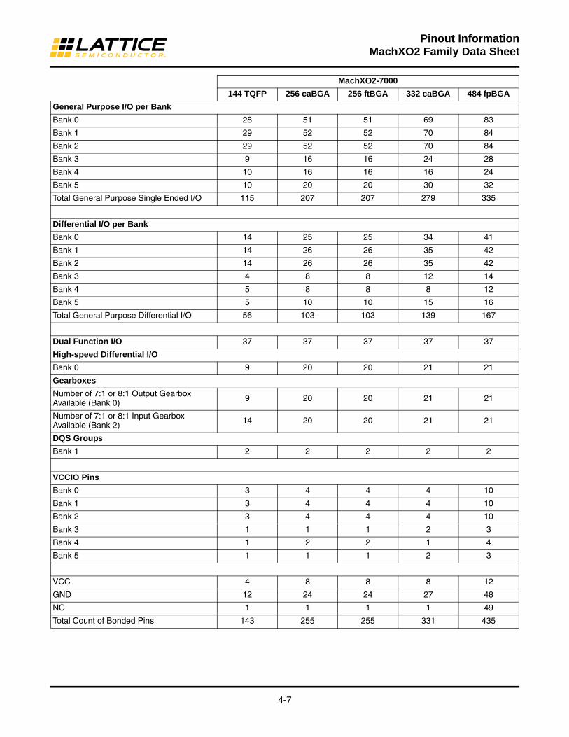
4-7
Pinout InformationMachXO2 Family Data Sheet
MachXO2-7000
144 TQFP 256 caBGA 256 ftBGA 332 caBGA 484 fpBGA
General Purpose I/O per Bank
Bank 0 28 51 51 69 83
Bank 1 29 52 52 70 84
Bank 2 29 52 52 70 84
Bank 3 9 16 16 24 28
Bank 4 10 16 16 16 24
Bank 5 10 20 20 30 32
Total General Purpose Single Ended I/O 115 207 207 279 335
Differential I/O per Bank
Bank 0 14 25 25 34 41
Bank 1 14 26 26 35 42
Bank 2 14 26 26 35 42
Bank 3 4 8 8 12 14
Bank 4 5 8 8 8 12
Bank 5 5 10 10 15 16
Total General Purpose Differential I/O 56 103 103 139 167
Dual Function I/O 37 37 37 37 37
High-speed Differential I/O
Bank 0 9 20 20 21 21
Gearboxes
Number of 7:1 or 8:1 Output Gearbox Available (Bank 0) 9 20 20 21 21
Number of 7:1 or 8:1 Input Gearbox Available (Bank 2) 14 20 20 21 21
DQS Groups
Bank 1 2 2 2 2 2
VCCIO Pins
Bank 0 3 4 4 4 10
Bank 1 3 4 4 4 10
Bank 2 3 4 4 4 10
Bank 3 1 1 1 2 3
Bank 4 1 2 2 1 4
Bank 5 1 1 1 2 3
VCC 4 8 8 8 12
GND 12 24 24 27 48
NC 1 1 1 1 49
Total Count of Bonded Pins 143 255 255 331 435

4-8
Pinout InformationMachXO2 Family Data Sheet
For Further InformationFor further information regarding logic signal connections for various packages please refer to the MachXO2 Device Pinout Files.
Thermal Management Thermal management is recommended as part of any sound FPGA design methodology. To assess the thermal characteristics of a system, Lattice specifies a maximum allowable junction temperature in all device data sheets. Users must complete a thermal analysis of their specific design to ensure that the device and package do not exceed the junction temperature limits. Refer to the Thermal Management document to find the device/package specific thermal values.
For Further InformationFor further information regarding Thermal Management, refer to the following:
• Thermal Management document
• TN1198, Power Estimation and Management for MachXO2 Devices
• The Power Calculator tool is included with the Lattice design tools, or as a standalone download fromwww.latticesemi.com/software

www.latticesemi.com 5-1 DS1035 Order Info_01.8
April 2012 Data Sheet DS1035
© 2012 Lattice Semiconductor Corp. All Lattice trademarks, registered trademarks, patents, and disclaimers are as listed at www.latticesemi.com/legal. All other brand or product names are trademarks or registered trademarks of their respective holders. The specifications and information herein are subject to change without notice.
MachXO2 Part Number Description
LCMXO2 – XXXX X X X – X XXXXXX X XX XX
Device Status Blank = Production Device ES = Engineering Sample R1 = Production Release 1 Device 50 = WLCSP package, 50 parts per reel Shipping Method Blank = Trays TR = Tape and Reel Grade C = Commercial I = Industrial
Logic Capacity 256 = 256 LUTs 640 = 640 LUTs 1200 = 1280 LUTs 2000 = 2112 LUTs 4000 = 4320 LUTs 7000 = 6864 LUTs
Power/Performance Z = Low Power H = High Performance
I/O Count Blank = Standard Device U = Ultra High I/O Device
Supply Voltage C = 2.5V/3.3V E = 1.2V
Speed 1 = Slowest 2 3 = Fastest
4 = Slowest 5 6 = Fastest
Low Power
High Performance
Package UWG25 = 25-Ball Halogen-Free WLCSP (0.4 mm Pitch) SG32 = 32-Pin Halogen-Free QFN (0.5 mm Pitch) UMG64 = 64-Ball Halogen-Free ucBGA (0.4 mm Pitch) TG100 = 100-Pin Halogen-Free TQFP TG144 = 144-Pin Halogen-Free TQFP MG132 = 132-Ball Halogen-Free csBGA (0.5 mm Pitch) BG256 = 256-Ball Halogen-Free caBGA (0.8 mm Pitch) FTG256 = 256-Ball Halogen-Free ftBGA (1.0 mm Pitch) BG332 = 332-Ball Halogen-Free caBGA FG484 = 484-Ball Halogen-Free fpBGA (1.0 mm Pitch)
Device Family MachXO2 PLD
Ordering InformationMachXO2 devices have top-side markings, for commercial and industrial grades, as shown below:
Notes:
1. Markings are abbreviated for small packages.
2. See PCN 05A-12 for information regarding a change to the top-side mark logo.
LCMXO2-1200ZE1TG100C Datecode
LCMXO2256ZE
1UG64CDatecode
MachXO2 Family Data SheetOrdering Information
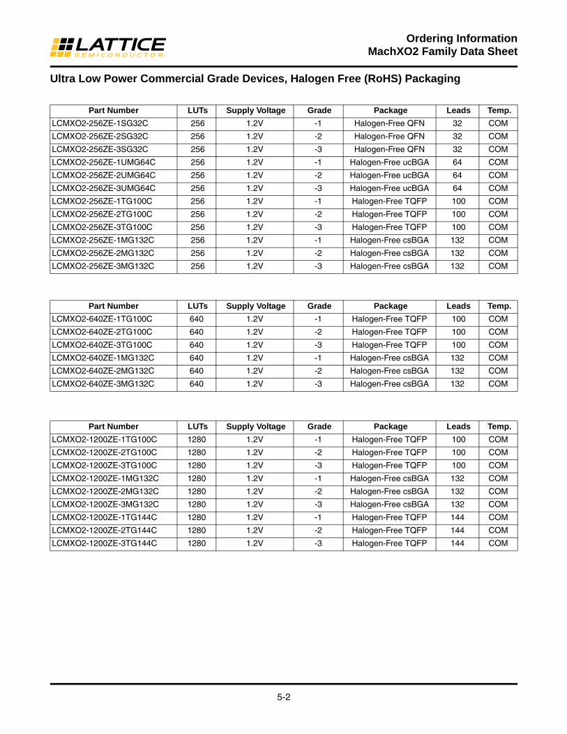
5-2
Ordering InformationMachXO2 Family Data Sheet
Ultra Low Power Commercial Grade Devices, Halogen Free (RoHS) Packaging
Part Number LUTs Supply Voltage Grade Package Leads Temp.
LCMXO2-256ZE-1SG32C 256 1.2V -1 Halogen-Free QFN 32 COM
LCMXO2-256ZE-2SG32C 256 1.2V -2 Halogen-Free QFN 32 COM
LCMXO2-256ZE-3SG32C 256 1.2V -3 Halogen-Free QFN 32 COM
LCMXO2-256ZE-1UMG64C 256 1.2V -1 Halogen-Free ucBGA 64 COM
LCMXO2-256ZE-2UMG64C 256 1.2V -2 Halogen-Free ucBGA 64 COM
LCMXO2-256ZE-3UMG64C 256 1.2V -3 Halogen-Free ucBGA 64 COM
LCMXO2-256ZE-1TG100C 256 1.2V -1 Halogen-Free TQFP 100 COM
LCMXO2-256ZE-2TG100C 256 1.2V -2 Halogen-Free TQFP 100 COM
LCMXO2-256ZE-3TG100C 256 1.2V -3 Halogen-Free TQFP 100 COM
LCMXO2-256ZE-1MG132C 256 1.2V -1 Halogen-Free csBGA 132 COM
LCMXO2-256ZE-2MG132C 256 1.2V -2 Halogen-Free csBGA 132 COM
LCMXO2-256ZE-3MG132C 256 1.2V -3 Halogen-Free csBGA 132 COM
Part Number LUTs Supply Voltage Grade Package Leads Temp.
LCMXO2-640ZE-1TG100C 640 1.2V -1 Halogen-Free TQFP 100 COM
LCMXO2-640ZE-2TG100C 640 1.2V -2 Halogen-Free TQFP 100 COM
LCMXO2-640ZE-3TG100C 640 1.2V -3 Halogen-Free TQFP 100 COM
LCMXO2-640ZE-1MG132C 640 1.2V -1 Halogen-Free csBGA 132 COM
LCMXO2-640ZE-2MG132C 640 1.2V -2 Halogen-Free csBGA 132 COM
LCMXO2-640ZE-3MG132C 640 1.2V -3 Halogen-Free csBGA 132 COM
Part Number LUTs Supply Voltage Grade Package Leads Temp.
LCMXO2-1200ZE-1TG100C 1280 1.2V -1 Halogen-Free TQFP 100 COM
LCMXO2-1200ZE-2TG100C 1280 1.2V -2 Halogen-Free TQFP 100 COM
LCMXO2-1200ZE-3TG100C 1280 1.2V -3 Halogen-Free TQFP 100 COM
LCMXO2-1200ZE-1MG132C 1280 1.2V -1 Halogen-Free csBGA 132 COM
LCMXO2-1200ZE-2MG132C 1280 1.2V -2 Halogen-Free csBGA 132 COM
LCMXO2-1200ZE-3MG132C 1280 1.2V -3 Halogen-Free csBGA 132 COM
LCMXO2-1200ZE-1TG144C 1280 1.2V -1 Halogen-Free TQFP 144 COM
LCMXO2-1200ZE-2TG144C 1280 1.2V -2 Halogen-Free TQFP 144 COM
LCMXO2-1200ZE-3TG144C 1280 1.2V -3 Halogen-Free TQFP 144 COM
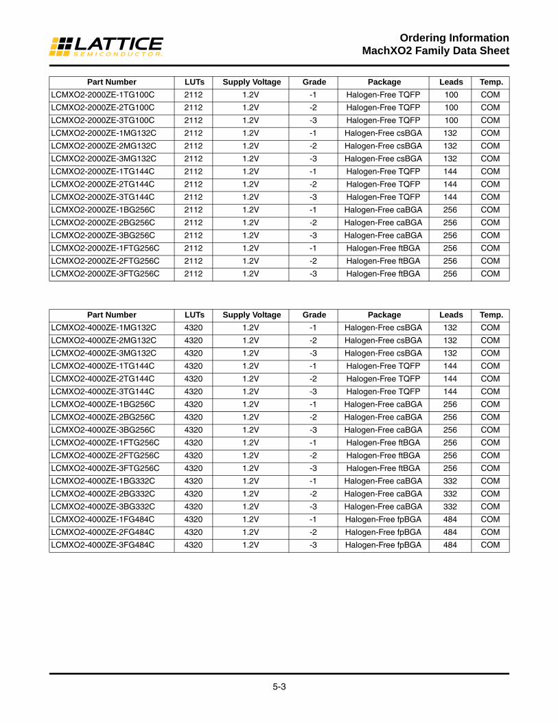
5-3
Ordering InformationMachXO2 Family Data Sheet
Part Number LUTs Supply Voltage Grade Package Leads Temp.
LCMXO2-2000ZE-1TG100C 2112 1.2V -1 Halogen-Free TQFP 100 COM
LCMXO2-2000ZE-2TG100C 2112 1.2V -2 Halogen-Free TQFP 100 COM
LCMXO2-2000ZE-3TG100C 2112 1.2V -3 Halogen-Free TQFP 100 COM
LCMXO2-2000ZE-1MG132C 2112 1.2V -1 Halogen-Free csBGA 132 COM
LCMXO2-2000ZE-2MG132C 2112 1.2V -2 Halogen-Free csBGA 132 COM
LCMXO2-2000ZE-3MG132C 2112 1.2V -3 Halogen-Free csBGA 132 COM
LCMXO2-2000ZE-1TG144C 2112 1.2V -1 Halogen-Free TQFP 144 COM
LCMXO2-2000ZE-2TG144C 2112 1.2V -2 Halogen-Free TQFP 144 COM
LCMXO2-2000ZE-3TG144C 2112 1.2V -3 Halogen-Free TQFP 144 COM
LCMXO2-2000ZE-1BG256C 2112 1.2V -1 Halogen-Free caBGA 256 COM
LCMXO2-2000ZE-2BG256C 2112 1.2V -2 Halogen-Free caBGA 256 COM
LCMXO2-2000ZE-3BG256C 2112 1.2V -3 Halogen-Free caBGA 256 COM
LCMXO2-2000ZE-1FTG256C 2112 1.2V -1 Halogen-Free ftBGA 256 COM
LCMXO2-2000ZE-2FTG256C 2112 1.2V -2 Halogen-Free ftBGA 256 COM
LCMXO2-2000ZE-3FTG256C 2112 1.2V -3 Halogen-Free ftBGA 256 COM
Part Number LUTs Supply Voltage Grade Package Leads Temp.
LCMXO2-4000ZE-1MG132C 4320 1.2V -1 Halogen-Free csBGA 132 COM
LCMXO2-4000ZE-2MG132C 4320 1.2V -2 Halogen-Free csBGA 132 COM
LCMXO2-4000ZE-3MG132C 4320 1.2V -3 Halogen-Free csBGA 132 COM
LCMXO2-4000ZE-1TG144C 4320 1.2V -1 Halogen-Free TQFP 144 COM
LCMXO2-4000ZE-2TG144C 4320 1.2V -2 Halogen-Free TQFP 144 COM
LCMXO2-4000ZE-3TG144C 4320 1.2V -3 Halogen-Free TQFP 144 COM
LCMXO2-4000ZE-1BG256C 4320 1.2V -1 Halogen-Free caBGA 256 COM
LCMXO2-4000ZE-2BG256C 4320 1.2V -2 Halogen-Free caBGA 256 COM
LCMXO2-4000ZE-3BG256C 4320 1.2V -3 Halogen-Free caBGA 256 COM
LCMXO2-4000ZE-1FTG256C 4320 1.2V -1 Halogen-Free ftBGA 256 COM
LCMXO2-4000ZE-2FTG256C 4320 1.2V -2 Halogen-Free ftBGA 256 COM
LCMXO2-4000ZE-3FTG256C 4320 1.2V -3 Halogen-Free ftBGA 256 COM
LCMXO2-4000ZE-1BG332C 4320 1.2V -1 Halogen-Free caBGA 332 COM
LCMXO2-4000ZE-2BG332C 4320 1.2V -2 Halogen-Free caBGA 332 COM
LCMXO2-4000ZE-3BG332C 4320 1.2V -3 Halogen-Free caBGA 332 COM
LCMXO2-4000ZE-1FG484C 4320 1.2V -1 Halogen-Free fpBGA 484 COM
LCMXO2-4000ZE-2FG484C 4320 1.2V -2 Halogen-Free fpBGA 484 COM
LCMXO2-4000ZE-3FG484C 4320 1.2V -3 Halogen-Free fpBGA 484 COM

5-4
Ordering InformationMachXO2 Family Data Sheet
High-Performance Commercial Grade Devices with Voltage Regulator, Halogen Free (RoHS) Packaging
Part Number LUTs Supply Voltage Grade Package Leads Temp.
LCMXO2-7000ZE-1TG144C 6864 1.2V -1 Halogen-Free TQFP 144 COM
LCMXO2-7000ZE-2TG144C 6864 1.2V -2 Halogen-Free TQFP 144 COM
LCMXO2-7000ZE-3TG144C 6864 1.2V -3 Halogen-Free TQFP 144 COM
LCMXO2-7000ZE-1BG256C 6864 1.2V -1 Halogen-Free caBGA 256 COM
LCMXO2-7000ZE-2BG256C 6864 1.2V -2 Halogen-Free caBGA 256 COM
LCMXO2-7000ZE-3BG256C 6864 1.2V -3 Halogen-Free caBGA 256 COM
LCMXO2-7000ZE-1FTG256C 6864 1.2V -1 Halogen-Free ftBGA 256 COM
LCMXO2-7000ZE-2FTG256C 6864 1.2V -2 Halogen-Free ftBGA 256 COM
LCMXO2-7000ZE-3FTG256C 6864 1.2V -3 Halogen-Free ftBGA 256 COM
LCMXO2-7000ZE-1BG332C 6864 1.2V -1 Halogen-Free caBGA 332 COM
LCMXO2-7000ZE-2BG332C 6864 1.2V -2 Halogen-Free caBGA 332 COM
LCMXO2-7000ZE-3BG332C 6864 1.2V -3 Halogen-Free caBGA 332 COM
LCMXO2-7000ZE-1FG484C 6864 1.2V -1 Halogen-Free fpBGA 484 COM
LCMXO2-7000ZE-2FG484C 6864 1.2V -2 Halogen-Free fpBGA 484 COM
LCMXO2-7000ZE-3FG484C 6864 1.2V -3 Halogen-Free fpBGA 484 COM
Part Number LUTs Supply Voltage Grade Package Leads Temp.
LCMXO2-1200ZE-1TG100CR11 1280 1.2V -1 Halogen-Free TQFP 100 COM
LCMXO2-1200ZE-2TG100CR11 1280 1.2V -2 Halogen-Free TQFP 100 COM
LCMXO2-1200ZE-3TG100CR11 1280 1.2V -3 Halogen-Free TQFP 100 COM
LCMXO2-1200ZE-1MG132CR11 1280 1.2V -1 Halogen-Free csBGA 132 COM
LCMXO2-1200ZE-2MG132CR11 1280 1.2V -2 Halogen-Free csBGA 132 COM
LCMXO2-1200ZE-3MG132CR11 1280 1.2V -3 Halogen-Free csBGA 132 COM
LCMXO2-1200ZE-1TG144CR11 1280 1.2V -1 Halogen-Free TQFP 144 COM
LCMXO2-1200ZE-2TG144CR11 1280 1.2V -2 Halogen-Free TQFP 144 COM
LCMXO2-1200ZE-3TG144CR11 1280 1.2V -3 Halogen-Free TQFP 144 COM
1. Specifications for the “LCMXO2-1200ZE-speed package CR1” are the same as the “LCMXO2-1200ZE-speed package C” devices respec-tively, except as specified in the R1 Device Specifications section on page 5-17 of this data sheet.
Part Number LUTs Supply Voltage Grade Package Leads Temp.
LCMXO2-256HC-4SG32C 256 2.5V/3.3V -4 Halogen-Free QFN 32 COM
LCMXO2-256HC-5SG32C 256 2.5V/3.3V -5 Halogen-Free QFN 32 COM
LCMXO2-256HC-6SG32C 256 2.5V/3.3V -6 Halogen-Free QFN 32 COM
LCMXO2-256HC-4UMG64C 256 2.5V/3.3V -4 Halogen-Free ucBGA 64 COM
LCMXO2-256HC-5UMG64C 256 2.5V/3.3V -5 Halogen-Free ucBGA 64 COM
LCMXO2-256HC-6UMG64C 256 2.5V/3.3V -6 Halogen-Free ucBGA 64 COM
LCMXO2-256HC-4TG100C 256 2.5V/3.3V -4 Halogen-Free TQFP 100 COM
LCMXO2-256HC-5TG100C 256 2.5V/3.3V -5 Halogen-Free TQFP 100 COM
LCMXO2-256HC-6TG100C 256 2.5V/3.3V -6 Halogen-Free TQFP 100 COM
LCMXO2-256HC-4MG132C 256 2.5V/3.3V -4 Halogen-Free csBGA 132 COM
LCMXO2-256HC-5MG132C 256 2.5V/3.3V -5 Halogen-Free csBGA 132 COM
LCMXO2-256HC-6MG132C 256 2.5V/3.3V -6 Halogen-Free csBGA 132 COM
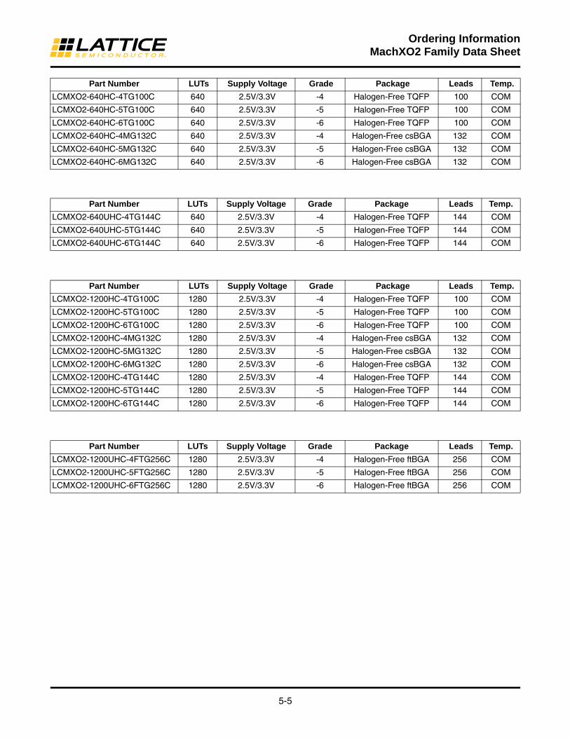
5-5
Ordering InformationMachXO2 Family Data Sheet
Part Number LUTs Supply Voltage Grade Package Leads Temp.
LCMXO2-640HC-4TG100C 640 2.5V/3.3V -4 Halogen-Free TQFP 100 COM
LCMXO2-640HC-5TG100C 640 2.5V/3.3V -5 Halogen-Free TQFP 100 COM
LCMXO2-640HC-6TG100C 640 2.5V/3.3V -6 Halogen-Free TQFP 100 COM
LCMXO2-640HC-4MG132C 640 2.5V/3.3V -4 Halogen-Free csBGA 132 COM
LCMXO2-640HC-5MG132C 640 2.5V/3.3V -5 Halogen-Free csBGA 132 COM
LCMXO2-640HC-6MG132C 640 2.5V/3.3V -6 Halogen-Free csBGA 132 COM
Part Number LUTs Supply Voltage Grade Package Leads Temp.
LCMXO2-640UHC-4TG144C 640 2.5V/3.3V -4 Halogen-Free TQFP 144 COM
LCMXO2-640UHC-5TG144C 640 2.5V/3.3V -5 Halogen-Free TQFP 144 COM
LCMXO2-640UHC-6TG144C 640 2.5V/3.3V -6 Halogen-Free TQFP 144 COM
Part Number LUTs Supply Voltage Grade Package Leads Temp.
LCMXO2-1200HC-4TG100C 1280 2.5V/3.3V -4 Halogen-Free TQFP 100 COM
LCMXO2-1200HC-5TG100C 1280 2.5V/3.3V -5 Halogen-Free TQFP 100 COM
LCMXO2-1200HC-6TG100C 1280 2.5V/3.3V -6 Halogen-Free TQFP 100 COM
LCMXO2-1200HC-4MG132C 1280 2.5V/3.3V -4 Halogen-Free csBGA 132 COM
LCMXO2-1200HC-5MG132C 1280 2.5V/3.3V -5 Halogen-Free csBGA 132 COM
LCMXO2-1200HC-6MG132C 1280 2.5V/3.3V -6 Halogen-Free csBGA 132 COM
LCMXO2-1200HC-4TG144C 1280 2.5V/3.3V -4 Halogen-Free TQFP 144 COM
LCMXO2-1200HC-5TG144C 1280 2.5V/3.3V -5 Halogen-Free TQFP 144 COM
LCMXO2-1200HC-6TG144C 1280 2.5V/3.3V -6 Halogen-Free TQFP 144 COM
Part Number LUTs Supply Voltage Grade Package Leads Temp.
LCMXO2-1200UHC-4FTG256C 1280 2.5V/3.3V -4 Halogen-Free ftBGA 256 COM
LCMXO2-1200UHC-5FTG256C 1280 2.5V/3.3V -5 Halogen-Free ftBGA 256 COM
LCMXO2-1200UHC-6FTG256C 1280 2.5V/3.3V -6 Halogen-Free ftBGA 256 COM

5-6
Ordering InformationMachXO2 Family Data Sheet
Part Number LUTs Supply Voltage Grade Package Leads Temp.
LCMXO2-2000HC-4TG100C 2112 2.5V/3.3V -4 Halogen-Free TQFP 100 COM
LCMXO2-2000HC-5TG100C 2112 2.5V/3.3V -5 Halogen-Free TQFP 100 COM
LCMXO2-2000HC-6TG100C 2112 2.5V/3.3V -6 Halogen-Free TQFP 100 COM
LCMXO2-2000HC-4MG132C 2112 2.5V/3.3V -4 Halogen-Free csBGA 132 COM
LCMXO2-2000HC-5MG132C 2112 2.5V/3.3V -5 Halogen-Free csBGA 132 COM
LCMXO2-2000HC-6MG132C 2112 2.5V/3.3V -6 Halogen-Free csBGA 132 COM
LCMXO2-2000HC-4TG144C 2112 2.5V/3.3V -4 Halogen-Free TQFP 144 COM
LCMXO2-2000HC-5TG144C 2112 2.5V/3.3V -5 Halogen-Free TQFP 144 COM
LCMXO2-2000HC-6TG144C 2112 2.5V/3.3V -6 Halogen-Free TQFP 144 COM
LCMXO2-2000HC-4BG256C 2112 2.5V/3.3V -4 Halogen-Free caBGA 256 COM
LCMXO2-2000HC-5BG256C 2112 2.5V/3.3V -5 Halogen-Free caBGA 256 COM
LCMXO2-2000HC-6BG256C 2112 2.5V/3.3V -6 Halogen-Free caBGA 256 COM
LCMXO2-2000HC-4FTG256C 2112 2.5V/3.3V -4 Halogen-Free ftBGA 256 COM
LCMXO2-2000HC-5FTG256C 2112 2.5V/3.3V -5 Halogen-Free ftBGA 256 COM
LCMXO2-2000HC-6FTG256C 2112 2.5V/3.3V -6 Halogen-Free ftBGA 256 COM
Part Number LUTs Supply Voltage Grade Package Leads Temp.
LCMXO2-2000UHC-4FG484C 2112 2.5V/3.3V -4 Halogen-Free fpBGA 484 COM
LCMXO2-2000UHC-5FG484C 2112 2.5V/3.3V -5 Halogen-Free fpBGA 484 COM
LCMXO2-2000UHC-6FG484C 2112 2.5V/3.3V -6 Halogen-Free fpBGA 484 COM
Part Number LUTs Supply Voltage Grade Package Leads Temp.
LCMXO2-4000HC-4MG132C 4320 2.5V/3.3V -4 Halogen-Free csBGA 132 COM
LCMXO2-4000HC-5MG132C 4320 2.5V/3.3V -5 Halogen-Free csBGA 132 COM
LCMXO2-4000HC-6MG132C 4320 2.5V/3.3V -6 Halogen-Free csBGA 132 COM
LCMXO2-4000HC-4TG144C 4320 2.5V/3.3V -4 Halogen-Free TQFP 144 COM
LCMXO2-4000HC-5TG144C 4320 2.5V/3.3V -5 Halogen-Free TQFP 144 COM
LCMXO2-4000HC-6TG144C 4320 2.5V/3.3V -6 Halogen-Free TQFP 144 COM
LCMXO2-4000HC-4BG256C 4320 2.5V/3.3V -4 Halogen-Free caBGA 256 COM
LCMXO2-4000HC-5BG256C 4320 2.5V/3.3V -5 Halogen-Free caBGA 256 COM
LCMXO2-4000HC-6BG256C 4320 2.5V/3.3V -6 Halogen-Free caBGA 256 COM
LCMXO2-4000HC-4FTG256C 4320 2.5V/3.3V -4 Halogen-Free ftBGA 256 COM
LCMXO2-4000HC-5FTG256C 4320 2.5V/3.3V -5 Halogen-Free ftBGA 256 COM
LCMXO2-4000HC-6FTG256C 4320 2.5V/3.3V -6 Halogen-Free ftBGA 256 COM
LCMXO2-4000HC-4BG332C 4320 2.5V/3.3V -4 Halogen-Free caBGA 332 COM
LCMXO2-4000HC-5BG332C 4320 2.5V/3.3V -5 Halogen-Free caBGA 332 COM
LCMXO2-4000HC-6BG332C 4320 2.5V/3.3V -6 Halogen-Free caBGA 332 COM
LCMXO2-4000HC-4FG484C 4320 2.5V/3.3V -4 Halogen-Free fpBGA 484 COM
LCMXO2-4000HC-5FG484C 4320 2.5V/3.3V -5 Halogen-Free fpBGA 484 COM
LCMXO2-4000HC-6FG484C 4320 2.5V/3.3V -6 Halogen-Free fpBGA 484 COM

5-7
Ordering InformationMachXO2 Family Data Sheet
Part Number LUTs Supply Voltage Grade Package Leads Temp.
LCMXO2-7000HC-4TG144C 6864 2.5V/3.3V -4 Halogen-Free TQFP 144 COM
LCMXO2-7000HC-5TG144C 6864 2.5V/3.3V -5 Halogen-Free TQFP 144 COM
LCMXO2-7000HC-6TG144C 6864 2.5V/3.3V -6 Halogen-Free TQFP 144 COM
LCMXO2-7000HC-4BG256C 6864 2.5V/3.3V -4 Halogen-Free caBGA 256 COM
LCMXO2-7000HC-5BG256C 6864 2.5V/3.3V -5 Halogen-Free caBGA 256 COM
LCMXO2-7000HC-6BG256C 6864 2.5V/3.3V -6 Halogen-Free caBGA 256 COM
LCMXO2-7000HC-4FTG256C 6864 2.5V/3.3V -4 Halogen-Free ftBGA 256 COM
LCMXO2-7000HC-5FTG256C 6864 2.5V/3.3V -5 Halogen-Free ftBGA 256 COM
LCMXO2-7000HC-6FTG256C 6864 2.5V/3.3V -6 Halogen-Free ftBGA 256 COM
LCMXO2-7000HC-4BG332C 6864 2.5V/3.3V -4 Halogen-Free caBGA 332 COM
LCMXO2-7000HC-5BG332C 6864 2.5V/3.3V -5 Halogen-Free caBGA 332 COM
LCMXO2-7000HC-6BG332C 6864 2.5V/3.3V -6 Halogen-Free caBGA 332 COM
LCMXO2-7000HC-4FG484C 6864 2.5V/3.3V -4 Halogen-Free fpBGA 484 COM
LCMXO2-7000HC-5FG484C 6864 2.5V/3.3V -5 Halogen-Free fpBGA 484 COM
LCMXO2-7000HC-6FG484C 6864 2.5V/3.3V -6 Halogen-Free fpBGA 484 COM
Part Number LUTs Supply Voltage Grade Package Leads Temp.
LCMXO2-1200HC-4TG100CR11 1280 2.5V/3.3V -4 Halogen-Free TQFP 100 COM
LCMXO2-1200HC-5TG100CR11 1280 2.5V/3.3V -5 Halogen-Free TQFP 100 COM
LCMXO2-1200HC-6TG100CR11 1280 2.5V/3.3V -6 Halogen-Free TQFP 100 COM
LCMXO2-1200HC-4MG132CR11 1280 2.5V/3.3V -4 Halogen-Free csBGA 132 COM
LCMXO2-1200HC-5MG132CR11 1280 2.5V/3.3V -5 Halogen-Free csBGA 132 COM
LCMXO2-1200HC-6MG132CR11 1280 2.5V/3.3V -6 Halogen-Free csBGA 132 COM
LCMXO2-1200HC-4TG144CR11 1280 2.5V/3.3V -4 Halogen-Free TQFP 144 COM
LCMXO2-1200HC-5TG144CR11 1280 2.5V/3.3V -5 Halogen-Free TQFP 144 COM
LCMXO2-1200HC-6TG144CR11 1280 2.5V/3.3V -6 Halogen-Free TQFP 144 COM
1. Specifications for the “LCMXO2-1200HC-speed package CR1” are the same as the “LCMXO2-1200HC-speed package C” devices respec-tively, except as specified in the R1 Device Specifications section on page 5-17 of this data sheet.
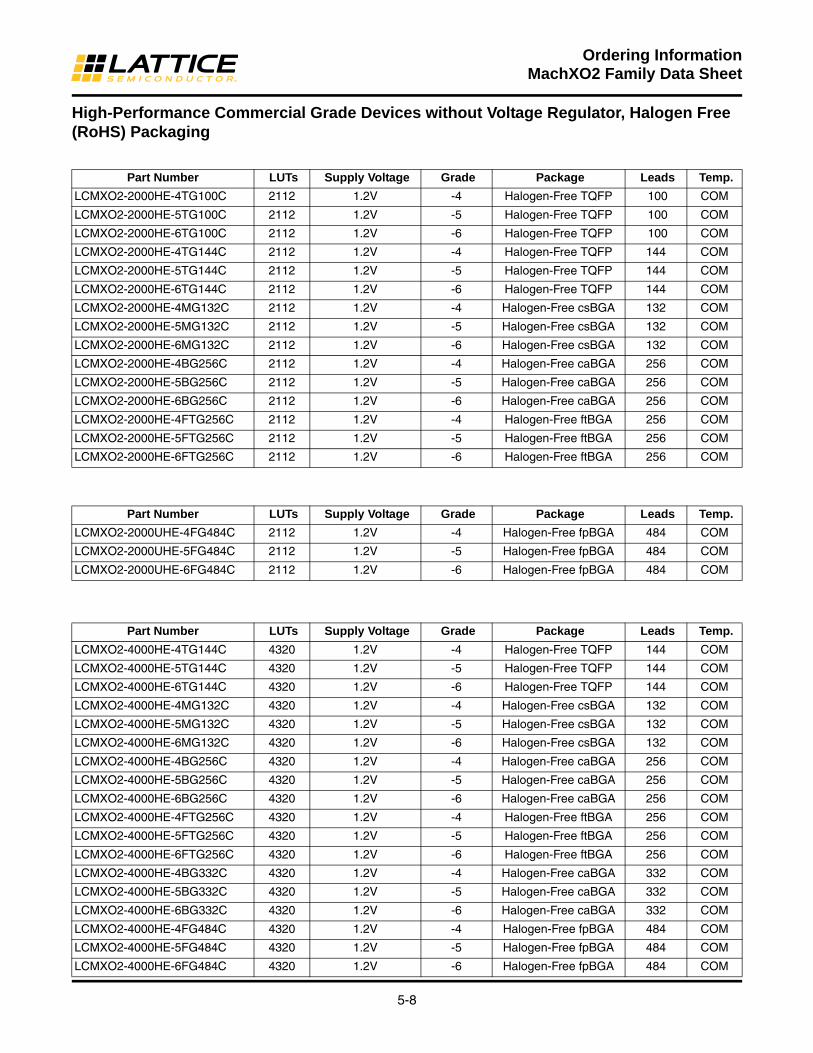
5-8
Ordering InformationMachXO2 Family Data Sheet
High-Performance Commercial Grade Devices without Voltage Regulator, Halogen Free (RoHS) Packaging
Part Number LUTs Supply Voltage Grade Package Leads Temp.
LCMXO2-2000HE-4TG100C 2112 1.2V -4 Halogen-Free TQFP 100 COM
LCMXO2-2000HE-5TG100C 2112 1.2V -5 Halogen-Free TQFP 100 COM
LCMXO2-2000HE-6TG100C 2112 1.2V -6 Halogen-Free TQFP 100 COM
LCMXO2-2000HE-4TG144C 2112 1.2V -4 Halogen-Free TQFP 144 COM
LCMXO2-2000HE-5TG144C 2112 1.2V -5 Halogen-Free TQFP 144 COM
LCMXO2-2000HE-6TG144C 2112 1.2V -6 Halogen-Free TQFP 144 COM
LCMXO2-2000HE-4MG132C 2112 1.2V -4 Halogen-Free csBGA 132 COM
LCMXO2-2000HE-5MG132C 2112 1.2V -5 Halogen-Free csBGA 132 COM
LCMXO2-2000HE-6MG132C 2112 1.2V -6 Halogen-Free csBGA 132 COM
LCMXO2-2000HE-4BG256C 2112 1.2V -4 Halogen-Free caBGA 256 COM
LCMXO2-2000HE-5BG256C 2112 1.2V -5 Halogen-Free caBGA 256 COM
LCMXO2-2000HE-6BG256C 2112 1.2V -6 Halogen-Free caBGA 256 COM
LCMXO2-2000HE-4FTG256C 2112 1.2V -4 Halogen-Free ftBGA 256 COM
LCMXO2-2000HE-5FTG256C 2112 1.2V -5 Halogen-Free ftBGA 256 COM
LCMXO2-2000HE-6FTG256C 2112 1.2V -6 Halogen-Free ftBGA 256 COM
Part Number LUTs Supply Voltage Grade Package Leads Temp.
LCMXO2-2000UHE-4FG484C 2112 1.2V -4 Halogen-Free fpBGA 484 COM
LCMXO2-2000UHE-5FG484C 2112 1.2V -5 Halogen-Free fpBGA 484 COM
LCMXO2-2000UHE-6FG484C 2112 1.2V -6 Halogen-Free fpBGA 484 COM
Part Number LUTs Supply Voltage Grade Package Leads Temp.
LCMXO2-4000HE-4TG144C 4320 1.2V -4 Halogen-Free TQFP 144 COM
LCMXO2-4000HE-5TG144C 4320 1.2V -5 Halogen-Free TQFP 144 COM
LCMXO2-4000HE-6TG144C 4320 1.2V -6 Halogen-Free TQFP 144 COM
LCMXO2-4000HE-4MG132C 4320 1.2V -4 Halogen-Free csBGA 132 COM
LCMXO2-4000HE-5MG132C 4320 1.2V -5 Halogen-Free csBGA 132 COM
LCMXO2-4000HE-6MG132C 4320 1.2V -6 Halogen-Free csBGA 132 COM
LCMXO2-4000HE-4BG256C 4320 1.2V -4 Halogen-Free caBGA 256 COM
LCMXO2-4000HE-5BG256C 4320 1.2V -5 Halogen-Free caBGA 256 COM
LCMXO2-4000HE-6BG256C 4320 1.2V -6 Halogen-Free caBGA 256 COM
LCMXO2-4000HE-4FTG256C 4320 1.2V -4 Halogen-Free ftBGA 256 COM
LCMXO2-4000HE-5FTG256C 4320 1.2V -5 Halogen-Free ftBGA 256 COM
LCMXO2-4000HE-6FTG256C 4320 1.2V -6 Halogen-Free ftBGA 256 COM
LCMXO2-4000HE-4BG332C 4320 1.2V -4 Halogen-Free caBGA 332 COM
LCMXO2-4000HE-5BG332C 4320 1.2V -5 Halogen-Free caBGA 332 COM
LCMXO2-4000HE-6BG332C 4320 1.2V -6 Halogen-Free caBGA 332 COM
LCMXO2-4000HE-4FG484C 4320 1.2V -4 Halogen-Free fpBGA 484 COM
LCMXO2-4000HE-5FG484C 4320 1.2V -5 Halogen-Free fpBGA 484 COM
LCMXO2-4000HE-6FG484C 4320 1.2V -6 Halogen-Free fpBGA 484 COM
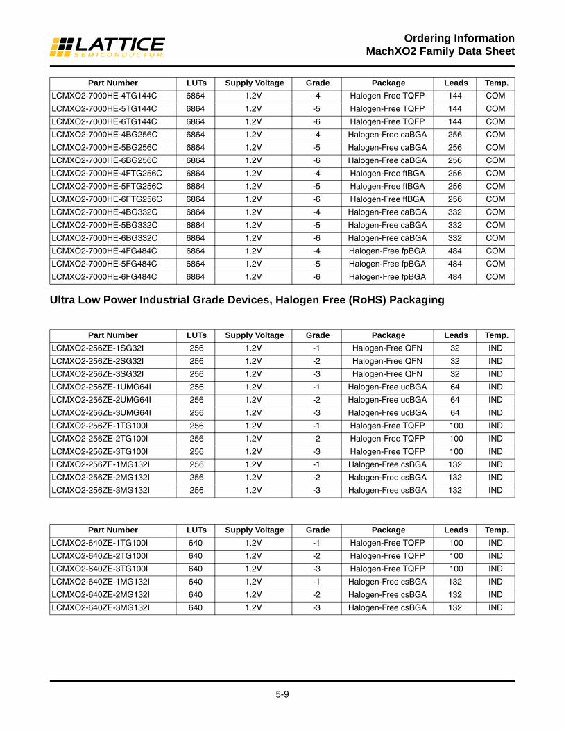
5-9
Ordering InformationMachXO2 Family Data Sheet
Ultra Low Power Industrial Grade Devices, Halogen Free (RoHS) Packaging
Part Number LUTs Supply Voltage Grade Package Leads Temp.
LCMXO2-7000HE-4TG144C 6864 1.2V -4 Halogen-Free TQFP 144 COM
LCMXO2-7000HE-5TG144C 6864 1.2V -5 Halogen-Free TQFP 144 COM
LCMXO2-7000HE-6TG144C 6864 1.2V -6 Halogen-Free TQFP 144 COM
LCMXO2-7000HE-4BG256C 6864 1.2V -4 Halogen-Free caBGA 256 COM
LCMXO2-7000HE-5BG256C 6864 1.2V -5 Halogen-Free caBGA 256 COM
LCMXO2-7000HE-6BG256C 6864 1.2V -6 Halogen-Free caBGA 256 COM
LCMXO2-7000HE-4FTG256C 6864 1.2V -4 Halogen-Free ftBGA 256 COM
LCMXO2-7000HE-5FTG256C 6864 1.2V -5 Halogen-Free ftBGA 256 COM
LCMXO2-7000HE-6FTG256C 6864 1.2V -6 Halogen-Free ftBGA 256 COM
LCMXO2-7000HE-4BG332C 6864 1.2V -4 Halogen-Free caBGA 332 COM
LCMXO2-7000HE-5BG332C 6864 1.2V -5 Halogen-Free caBGA 332 COM
LCMXO2-7000HE-6BG332C 6864 1.2V -6 Halogen-Free caBGA 332 COM
LCMXO2-7000HE-4FG484C 6864 1.2V -4 Halogen-Free fpBGA 484 COM
LCMXO2-7000HE-5FG484C 6864 1.2V -5 Halogen-Free fpBGA 484 COM
LCMXO2-7000HE-6FG484C 6864 1.2V -6 Halogen-Free fpBGA 484 COM
Part Number LUTs Supply Voltage Grade Package Leads Temp.
LCMXO2-256ZE-1SG32I 256 1.2V -1 Halogen-Free QFN 32 IND
LCMXO2-256ZE-2SG32I 256 1.2V -2 Halogen-Free QFN 32 IND
LCMXO2-256ZE-3SG32I 256 1.2V -3 Halogen-Free QFN 32 IND
LCMXO2-256ZE-1UMG64I 256 1.2V -1 Halogen-Free ucBGA 64 IND
LCMXO2-256ZE-2UMG64I 256 1.2V -2 Halogen-Free ucBGA 64 IND
LCMXO2-256ZE-3UMG64I 256 1.2V -3 Halogen-Free ucBGA 64 IND
LCMXO2-256ZE-1TG100I 256 1.2V -1 Halogen-Free TQFP 100 IND
LCMXO2-256ZE-2TG100I 256 1.2V -2 Halogen-Free TQFP 100 IND
LCMXO2-256ZE-3TG100I 256 1.2V -3 Halogen-Free TQFP 100 IND
LCMXO2-256ZE-1MG132I 256 1.2V -1 Halogen-Free csBGA 132 IND
LCMXO2-256ZE-2MG132I 256 1.2V -2 Halogen-Free csBGA 132 IND
LCMXO2-256ZE-3MG132I 256 1.2V -3 Halogen-Free csBGA 132 IND
Part Number LUTs Supply Voltage Grade Package Leads Temp.
LCMXO2-640ZE-1TG100I 640 1.2V -1 Halogen-Free TQFP 100 IND
LCMXO2-640ZE-2TG100I 640 1.2V -2 Halogen-Free TQFP 100 IND
LCMXO2-640ZE-3TG100I 640 1.2V -3 Halogen-Free TQFP 100 IND
LCMXO2-640ZE-1MG132I 640 1.2V -1 Halogen-Free csBGA 132 IND
LCMXO2-640ZE-2MG132I 640 1.2V -2 Halogen-Free csBGA 132 IND
LCMXO2-640ZE-3MG132I 640 1.2V -3 Halogen-Free csBGA 132 IND

5-10
Ordering InformationMachXO2 Family Data Sheet
Part Number LUTs Supply Voltage Grade Package Leads Temp.
LCMXO2-1200ZE-1UWG25ITR1 1280 1.2V -1 Halogen-Free WLCSP 25 IND
LCMXO2-1200ZE-1UWG25ITR502 1280 1.2V -1 Halogen-Free WLCSP 25 IND
LCMXO2-1200ZE-1TG100I 1280 1.2V -1 Halogen-Free TQFP 100 IND
LCMXO2-1200ZE-2TG100I 1280 1.2V -2 Halogen-Free TQFP 100 IND
LCMXO2-1200ZE-3TG100I 1280 1.2V -3 Halogen-Free TQFP 100 IND
LCMXO2-1200ZE-1MG132I 1280 1.2V -1 Halogen-Free csBGA 132 IND
LCMXO2-1200ZE-2MG132I 1280 1.2V -2 Halogen-Free csBGA 132 IND
LCMXO2-1200ZE-3MG132I 1280 1.2V -3 Halogen-Free csBGA 132 IND
LCMXO2-1200ZE-1TG144I 1280 1.2V -1 Halogen-Free TQFP 144 IND
LCMXO2-1200ZE-2TG144I 1280 1.2V -2 Halogen-Free TQFP 144 IND
LCMXO2-1200ZE-3TG144I 1280 1.2V -3 Halogen-Free TQFP 144 IND
1. This part number has a tape and reel quantity of 5,000 units with a minimum order quantity of 10,000 units. Order quantities must be in increments of 10,000 units. For example, a 10,000 unit order will be shipped in two reels with one reel containing 5,000 units and the other reel with less than 5,000 units (depending on test yields). Unserviced backlog will be canceled.
2. This part number has a tape and reel quantity of 50 units with a minimum order quantity of 50. Order quantities must be in increments of 50 units. For example, a 1000 unit order will be shipped as 20 reels of 50 units each.
Part Number LUTs Supply Voltage Grade Package Leads Temp.
LCMXO2-2000ZE-1TG100I 2112 1.2V -1 Halogen-Free TQFP 100 IND
LCMXO2-2000ZE-2TG100I 2112 1.2V -2 Halogen-Free TQFP 100 IND
LCMXO2-2000ZE-3TG100I 2112 1.2V -3 Halogen-Free TQFP 100 IND
LCMXO2-2000ZE-1MG132I 2112 1.2V -1 Halogen-Free csBGA 132 IND
LCMXO2-2000ZE-2MG132I 2112 1.2V -2 Halogen-Free csBGA 132 IND
LCMXO2-2000ZE-3MG132I 2112 1.2V -3 Halogen-Free csBGA 132 IND
LCMXO2-2000ZE-1TG144I 2112 1.2V -1 Halogen-Free TQFP 144 IND
LCMXO2-2000ZE-2TG144I 2112 1.2V -2 Halogen-Free TQFP 144 IND
LCMXO2-2000ZE-3TG144I 2112 1.2V -3 Halogen-Free TQFP 144 IND
LCMXO2-2000ZE-1BG256I 2112 1.2V -1 Halogen-Free caBGA 256 IND
LCMXO2-2000ZE-2BG256I 2112 1.2V -2 Halogen-Free caBGA 256 IND
LCMXO2-2000ZE-3BG256I 2112 1.2V -3 Halogen-Free caBGA 256 IND
LCMXO2-2000ZE-1FTG256I 2112 1.2V -1 Halogen-Free ftBGA 256 IND
LCMXO2-2000ZE-2FTG256I 2112 1.2V -2 Halogen-Free ftBGA 256 IND
LCMXO2-2000ZE-3FTG256I 2112 1.2V -3 Halogen-Free ftBGA 256 IND
1. Samples can be ordered in minimum order quantities and increments of 50 units. Production volumes can be ordered in minimum order quantities and increments of 10,000 units for the LCMXO2-1200ZE in the 25-ball WLCSP package.

5-11
Ordering InformationMachXO2 Family Data Sheet
Part Number LUTs Supply Voltage Grade Package Leads Temp.
LCMXO2-4000ZE-1MG132I 4320 1.2V -1 Halogen-Free csBGA 132 IND
LCMXO2-4000ZE-2MG132I 4320 1.2V -2 Halogen-Free csBGA 132 IND
LCMXO2-4000ZE-3MG132I 4320 1.2V -3 Halogen-Free csBGA 132 IND
LCMXO2-4000ZE-1TG144I 4320 1.2V -1 Halogen-Free TQFP 144 IND
LCMXO2-4000ZE-2TG144I 4320 1.2V -2 Halogen-Free TQFP 144 IND
LCMXO2-4000ZE-3TG144I 4320 1.2V -3 Halogen-Free TQFP 144 IND
LCMXO2-4000ZE-1BG256I 4320 1.2V -1 Halogen-Free caBGA 256 IND
LCMXO2-4000ZE-2BG256I 4320 1.2V -2 Halogen-Free caBGA 256 IND
LCMXO2-4000ZE-3BG256I 4320 1.2V -3 Halogen-Free caBGA 256 IND
LCMXO2-4000ZE-1FTG256I 4320 1.2V -1 Halogen-Free ftBGA 256 IND
LCMXO2-4000ZE-2FTG256I 4320 1.2V -2 Halogen-Free ftBGA 256 IND
LCMXO2-4000ZE-3FTG256I 4320 1.2V -3 Halogen-Free ftBGA 256 IND
LCMXO2-4000ZE-1BG332I 4320 1.2V -1 Halogen-Free caBGA 332 IND
LCMXO2-4000ZE-2BG332I 4320 1.2V -2 Halogen-Free caBGA 332 IND
LCMXO2-4000ZE-3BG332I 4320 1.2V -3 Halogen-Free caBGA 332 IND
LCMXO2-4000ZE-1FG484I 4320 1.2V -1 Halogen-Free fpBGA 484 IND
LCMXO2-4000ZE-2FG484I 4320 1.2V -2 Halogen-Free fpBGA 484 IND
LCMXO2-4000ZE-3FG484I 4320 1.2V -3 Halogen-Free fpBGA 484 IND
Part Number LUTs Supply Voltage Grade Package Leads Temp.
LCMXO2-7000ZE-1TG144I 6864 1.2V -1 Halogen-Free TQFP 144 IND
LCMXO2-7000ZE-2TG144I 6864 1.2V -2 Halogen-Free TQFP 144 IND
LCMXO2-7000ZE-3TG144I 6864 1.2V -3 Halogen-Free TQFP 144 IND
LCMXO2-7000ZE-1BG256I 6864 1.2V -1 Halogen-Free caBGA 256 IND
LCMXO2-7000ZE-2BG256I 6864 1.2V -2 Halogen-Free caBGA 256 IND
LCMXO2-7000ZE-3BG256I 6864 1.2V -3 Halogen-Free caBGA 256 IND
LCMXO2-7000ZE-1FTG256I 6864 1.2V -1 Halogen-Free ftBGA 256 IND
LCMXO2-7000ZE-2FTG256I 6864 1.2V -2 Halogen-Free ftBGA 256 IND
LCMXO2-7000ZE-3FTG256I 6864 1.2V -3 Halogen-Free ftBGA 256 IND
LCMXO2-7000ZE-1BG332I 6864 1.2V -1 Halogen-Free caBGA 332 IND
LCMXO2-7000ZE-2BG332I 6864 1.2V -2 Halogen-Free caBGA 332 IND
LCMXO2-7000ZE-3BG332I 6864 1.2V -3 Halogen-Free caBGA 332 IND
LCMXO2-7000ZE-1FG484I 6864 1.2V -1 Halogen-Free fpBGA 484 IND
LCMXO2-7000ZE-2FG484I 6864 1.2V -2 Halogen-Free fpBGA 484 IND
LCMXO2-7000ZE-3FG484I 6864 1.2V -3 Halogen-Free fpBGA 484 IND
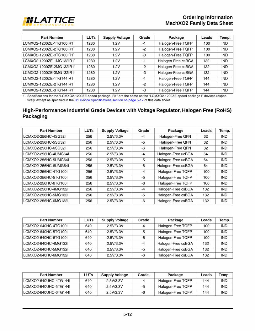
5-12
Ordering InformationMachXO2 Family Data Sheet
High-Performance Industrial Grade Devices with Voltage Regulator, Halogen Free (RoHS) Packaging
Part Number LUTs Supply Voltage Grade Package Leads Temp.
LCMXO2-1200ZE-1TG100IR11 1280 1.2V -1 Halogen-Free TQFP 100 IND
LCMXO2-1200ZE-2TG100IR11 1280 1.2V -2 Halogen-Free TQFP 100 IND
LCMXO2-1200ZE-3TG100IR11 1280 1.2V -3 Halogen-Free TQFP 100 IND
LCMXO2-1200ZE-1MG132IR11 1280 1.2V -1 Halogen-Free csBGA 132 IND
LCMXO2-1200ZE-2MG132IR11 1280 1.2V -2 Halogen-Free csBGA 132 IND
LCMXO2-1200ZE-3MG132IR11 1280 1.2V -3 Halogen-Free csBGA 132 IND
LCMXO2-1200ZE-1TG144IR11 1280 1.2V -1 Halogen-Free TQFP 144 IND
LCMXO2-1200ZE-2TG144IR11 1280 1.2V -2 Halogen-Free TQFP 144 IND
LCMXO2-1200ZE-3TG144IR11 1280 1.2V -3 Halogen-Free TQFP 144 IND
1. Specifications for the “LCMXO2-1200ZE-speed package IR1” are the same as the “LCMXO2-1200ZE-speed package I” devices respec-tively, except as specified in the R1 Device Specifications section on page 5-17 of this data sheet.
Part Number LUTs Supply Voltage Grade Package Leads Temp.
LCMXO2-256HC-4SG32I 256 2.5V/3.3V -4 Halogen-Free QFN 32 IND
LCMXO2-256HC-5SG32I 256 2.5V/3.3V -5 Halogen-Free QFN 32 IND
LCMXO2-256HC-6SG32I 256 2.5V/3.3V -6 Halogen-Free QFN 32 IND
LCMXO2-256HC-4UMG64I 256 2.5V/3.3V -4 Halogen-Free ucBGA 64 IND
LCMXO2-256HC-5UMG64I 256 2.5V/3.3V -5 Halogen-Free ucBGA 64 IND
LCMXO2-256HC-6UMG64I 256 2.5V/3.3V -6 Halogen-Free ucBGA 64 IND
LCMXO2-256HC-4TG100I 256 2.5V/3.3V -4 Halogen-Free TQFP 100 IND
LCMXO2-256HC-5TG100I 256 2.5V/3.3V -5 Halogen-Free TQFP 100 IND
LCMXO2-256HC-6TG100I 256 2.5V/3.3V -6 Halogen-Free TQFP 100 IND
LCMXO2-256HC-4MG132I 256 2.5V/3.3V -4 Halogen-Free csBGA 132 IND
LCMXO2-256HC-5MG132I 256 2.5V/3.3V -5 Halogen-Free csBGA 132 IND
LCMXO2-256HC-6MG132I 256 2.5V/3.3V -6 Halogen-Free csBGA 132 IND
Part Number LUTs Supply Voltage Grade Package Leads Temp.
LCMXO2-640HC-4TG100I 640 2.5V/3.3V -4 Halogen-Free TQFP 100 IND
LCMXO2-640HC-5TG100I 640 2.5V/3.3V -5 Halogen-Free TQFP 100 IND
LCMXO2-640HC-6TG100I 640 2.5V/3.3V -6 Halogen-Free TQFP 100 IND
LCMXO2-640HC-4MG132I 640 2.5V/3.3V -4 Halogen-Free csBGA 132 IND
LCMXO2-640HC-5MG132I 640 2.5V/3.3V -5 Halogen-Free csBGA 132 IND
LCMXO2-640HC-6MG132I 640 2.5V/3.3V -6 Halogen-Free csBGA 132 IND
Part Number LUTs Supply Voltage Grade Package Leads Temp.
LCMXO2-640UHC-4TG144I 640 2.5V/3.3V -4 Halogen-Free TQFP 144 IND
LCMXO2-640UHC-5TG144I 640 2.5V/3.3V -5 Halogen-Free TQFP 144 IND
LCMXO2-640UHC-6TG144I 640 2.5V/3.3V -6 Halogen-Free TQFP 144 IND

5-13
Ordering InformationMachXO2 Family Data Sheet
Part Number LUTs Supply Voltage Grade Package Leads Temp.
LCMXO2-1200HC-4TG100I 1280 2.5V/3.3V -4 Halogen-Free TQFP 100 IND
LCMXO2-1200HC-5TG100I 1280 2.5V/3.3V -5 Halogen-Free TQFP 100 IND
LCMXO2-1200HC-6TG100I 1280 2.5V/3.3V -6 Halogen-Free TQFP 100 IND
LCMXO2-1200HC-4MG132I 1280 2.5V/3.3V -4 Halogen-Free csBGA 132 IND
LCMXO2-1200HC-5MG132I 1280 2.5V/3.3V -5 Halogen-Free csBGA 132 IND
LCMXO2-1200HC-6MG132I 1280 2.5V/3.3V -6 Halogen-Free csBGA 132 IND
LCMXO2-1200HC-4TG144I 1280 2.5V/3.3V -4 Halogen-Free TQFP 144 IND
LCMXO2-1200HC-5TG144I 1280 2.5V/3.3V -5 Halogen-Free TQFP 144 IND
LCMXO2-1200HC-6TG144I 1280 2.5V/3.3V -6 Halogen-Free TQFP 144 IND
Part Number LUTs Supply Voltage Grade Package Leads Temp.
LCMXO2-1200UHC-4FTG256I 1280 2.5V/3.3V -4 Halogen-Free ftBGA 256 IND
LCMXO2-1200UHC-5FTG256I 1280 2.5V/3.3V -5 Halogen-Free ftBGA 256 IND
LCMXO2-1200UHC-6FTG256I 1280 2.5V/3.3V -6 Halogen-Free ftBGA 256 IND
Part Number LUTs Supply Voltage Grade Package Leads Temp.
LCMXO2-2000HC-4TG100I 2112 2.5V/3.3V -4 Halogen-Free TQFP 100 IND
LCMXO2-2000HC-5TG100I 2112 2.5V/3.3V -5 Halogen-Free TQFP 100 IND
LCMXO2-2000HC-6TG100I 2112 2.5V/3.3V -6 Halogen-Free TQFP 100 IND
LCMXO2-2000HC-4MG132I 2112 2.5V/3.3V -4 Halogen-Free csBGA 132 IND
LCMXO2-2000HC-5MG132I 2112 2.5V/3.3V -5 Halogen-Free csBGA 132 IND
LCMXO2-2000HC-6MG132I 2112 2.5V/3.3V -6 Halogen-Free csBGA 132 IND
LCMXO2-2000HC-4TG144I 2112 2.5V/3.3V -4 Halogen-Free TQFP 144 IND
LCMXO2-2000HC-5TG144I 2112 2.5V/3.3V -5 Halogen-Free TQFP 144 IND
LCMXO2-2000HC-6TG144I 2112 2.5V/3.3V -6 Halogen-Free TQFP 144 IND
LCMXO2-2000HC-4BG256I 2112 2.5V/3.3V -4 Halogen-Free caBGA 256 IND
LCMXO2-2000HC-5BG256I 2112 2.5V/3.3V -5 Halogen-Free caBGA 256 IND
LCMXO2-2000HC-6BG256I 2112 2.5V/3.3V -6 Halogen-Free caBGA 256 IND
LCMXO2-2000HC-4FTG256I 2112 2.5V/3.3V -4 Halogen-Free ftBGA 256 IND
LCMXO2-2000HC-5FTG256I 2112 2.5V/3.3V -5 Halogen-Free ftBGA 256 IND
LCMXO2-2000HC-6FTG256I 2112 2.5V/3.3V -6 Halogen-Free ftBGA 256 IND
Part Number LUTs Supply Voltage Grade Package Leads Temp.
LCMXO2-2000UHC-4FG484I 2112 2.5V/3.3V -4 Halogen-Free fpBGA 484 IND
LCMXO2-2000UHC-5FG484I 2112 2.5V/3.3V -5 Halogen-Free fpBGA 484 IND
LCMXO2-2000UHC-6FG484I 2112 2.5V/3.3V -6 Halogen-Free fpBGA 484 IND

5-14
Ordering InformationMachXO2 Family Data Sheet
Part Number LUTs Supply Voltage Grade Package Leads Temp.
LCMXO2-4000HC-4TG144I 4320 2.5V/3.3V -4 Halogen-Free TQFP 144 IND
LCMXO2-4000HC-5TG144I 4320 2.5V/3.3V -5 Halogen-Free TQFP 144 IND
LCMXO2-4000HC-6TG144I 4320 2.5V/3.3V -6 Halogen-Free TQFP 144 IND
LCMXO2-4000HC-4MG132I 4320 2.5V/3.3V -4 Halogen-Free csBGA 132 IND
LCMXO2-4000HC-5MG132I 4320 2.5V/3.3V -5 Halogen-Free csBGA 132 IND
LCMXO2-4000HC-6MG132I 4320 2.5V/3.3V -6 Halogen-Free csBGA 132 IND
LCMXO2-4000HC-4BG256I 4320 2.5V/3.3V -4 Halogen-Free caBGA 256 IND
LCMXO2-4000HC-5BG256I 4320 2.5V/3.3V -5 Halogen-Free caBGA 256 IND
LCMXO2-4000HC-6BG256I 4320 2.5V/3.3V -6 Halogen-Free caBGA 256 IND
LCMXO2-4000HC-4FTG256I 4320 2.5V/3.3V -4 Halogen-Free ftBGA 256 IND
LCMXO2-4000HC-5FTG256I 4320 2.5V/3.3V -5 Halogen-Free ftBGA 256 IND
LCMXO2-4000HC-6FTG256I 4320 2.5V/3.3V -6 Halogen-Free ftBGA 256 IND
LCMXO2-4000HC-4BG332I 4320 2.5V/3.3V -4 Halogen-Free caBGA 332 IND
LCMXO2-4000HC-5BG332I 4320 2.5V/3.3V -5 Halogen-Free caBGA 332 IND
LCMXO2-4000HC-6BG332I 4320 2.5V/3.3V -6 Halogen-Free caBGA 332 IND
LCMXO2-4000HC-4FG484I 4320 2.5V/3.3V -4 Halogen-Free fpBGA 484 IND
LCMXO2-4000HC-5FG484I 4320 2.5V/3.3V -5 Halogen-Free fpBGA 484 IND
LCMXO2-4000HC-6FG484I 4320 2.5V/3.3V -6 Halogen-Free fpBGA 484 IND
Part Number LUTs Supply Voltage Grade Package Leads Temp.
LCMXO2-7000HC-4TG144I 6864 2.5V/3.3V -4 Halogen-Free TQFP 144 IND
LCMXO2-7000HC-5TG144I 6864 2.5V/3.3V -5 Halogen-Free TQFP 144 IND
LCMXO2-7000HC-6TG144I 6864 2.5V/3.3V -6 Halogen-Free TQFP 144 IND
LCMXO2-7000HC-4BG256I 6864 2.5V/3.3V -4 Halogen-Free caBGA 256 IND
LCMXO2-7000HC-5BG256I 6864 2.5V/3.3V -5 Halogen-Free caBGA 256 IND
LCMXO2-7000HC-6BG256I 6864 2.5V/3.3V -6 Halogen-Free caBGA 256 IND
LCMXO2-7000HC-4FTG256I 6864 2.5V/3.3V -4 Halogen-Free ftBGA 256 IND
LCMXO2-7000HC-5FTG256I 6864 2.5V/3.3V -5 Halogen-Free ftBGA 256 IND
LCMXO2-7000HC-6FTG256I 6864 2.5V/3.3V -6 Halogen-Free ftBGA 256 IND
LCMXO2-7000HC-4BG332I 6864 2.5V/3.3V -4 Halogen-Free caBGA 332 IND
LCMXO2-7000HC-5BG332I 6864 2.5V/3.3V -5 Halogen-Free caBGA 332 IND
LCMXO2-7000HC-6BG332I 6864 2.5V/3.3V -6 Halogen-Free caBGA 332 IND
LCMXO2-7000HC-4FG484I 6864 2.5V/3.3V -4 Halogen-Free fpBGA 484 IND
LCMXO2-7000HC-5FG484I 6864 2.5V/3.3V -5 Halogen-Free fpBGA 484 IND
LCMXO2-7000HC-6FG484I 6864 2.5V/3.3V -6 Halogen-Free fpBGA 484 IND

5-15
Ordering InformationMachXO2 Family Data Sheet
High Performance Industrial Grade Devices Without Voltage Regulator, Halogen Free (RoHS) Packaging
Part Number LUTs Supply Voltage Grade Package Leads Temp.
LCMXO2-1200HC-4TG100IR11 1280 2.5V/3.3V -4 Halogen-Free TQFP 100 IND
LCMXO2-1200HC-5TG100IR11 1280 2.5V/3.3V -5 Halogen-Free TQFP 100 IND
LCMXO2-1200HC-6TG100IR11 1280 2.5V/3.3V -6 Halogen-Free TQFP 100 IND
LCMXO2-1200HC-4MG132IR11 1280 2.5V/3.3V -4 Halogen-Free csBGA 132 IND
LCMXO2-1200HC-5MG132IR11 1280 2.5V/3.3V -5 Halogen-Free csBGA 132 IND
LCMXO2-1200HC-6MG132IR11 1280 2.5V/3.3V -6 Halogen-Free csBGA 132 IND
LCMXO2-1200HC-4TG144IR11 1280 2.5V/3.3V -4 Halogen-Free TQFP 144 IND
LCMXO2-1200HC-5TG144IR11 1280 2.5V/3.3V -5 Halogen-Free TQFP 144 IND
LCMXO2-1200HC-6TG144IR11 1280 2.5V/3.3V -6 Halogen-Free TQFP 144 IND
1. Specifications for the “LCMXO2-1200HC-speed package IR1” are the same as the “LCMXO2-1200ZE-speed package I” devices respec-tively, except as specified in the R1 Device Specifications section on page 5-17 of this data sheet.
Part Number LUTs Supply Voltage Grade Package Leads Temp.
LCMXO2-2000HE-4TG100I 2112 1.2V -4 Halogen-Free TQFP 100 IND
LCMXO2-2000HE-5TG100I 2112 1.2V -5 Halogen-Free TQFP 100 IND
LCMXO2-2000HE-6TG100I 2112 1.2V -6 Halogen-Free TQFP 100 IND
LCMXO2-2000HE-4MG132I 2112 1.2V -4 Halogen-Free csBGA 132 IND
LCMXO2-2000HE-5MG132I 2112 1.2V -5 Halogen-Free csBGA 132 IND
LCMXO2-2000HE-6MG132I 2112 1.2V -6 Halogen-Free csBGA 132 IND
LCMXO2-2000HE-4TG144I 2112 1.2V -4 Halogen-Free TQFP 144 IND
LCMXO2-2000HE-5TG144I 2112 1.2V -5 Halogen-Free TQFP 144 IND
LCMXO2-2000HE-6TG144I 2112 1.2V -6 Halogen-Free TQFP 144 IND
LCMXO2-2000HE-4BG256I 2112 1.2V -4 Halogen-Free caBGA 256 IND
LCMXO2-2000HE-5BG256I 2112 1.2V -5 Halogen-Free caBGA 256 IND
LCMXO2-2000HE-6BG256I 2112 1.2V -6 Halogen-Free caBGA 256 IND
LCMXO2-2000HE-4FTG256I 2112 1.2V -4 Halogen-Free ftBGA 256 IND
LCMXO2-2000HE-5FTG256I 2112 1.2V -5 Halogen-Free ftBGA 256 IND
LCMXO2-2000HE-6FTG256I 2112 1.2V -6 Halogen-Free ftBGA 256 IND
Part Number LUTs Supply Voltage Grade Package Leads Temp.
LCMXO2-2000UHE-4FG484I 2112 1.2V -4 Halogen-Free fpBGA 484 IND
LCMXO2-2000UHE-5FG484I 2112 1.2V -5 Halogen-Free fpBGA 484 IND
LCMXO2-2000UHE-6FG484I 2112 1.2V -6 Halogen-Free fpBGA 484 IND

5-16
Ordering InformationMachXO2 Family Data Sheet
Part Number LUTs Supply Voltage Grade Package Leads Temp.
LCMXO2-4000HE-4MG132I 4320 1.2V -4 Halogen-Free csBGA 132 IND
LCMXO2-4000HE-5MG132I 4320 1.2V -5 Halogen-Free csBGA 132 IND
LCMXO2-4000HE-6MG132I 4320 1.2V -6 Halogen-Free csBGA 132 IND
LCMXO2-4000HE-4TG144I 4320 1.2V -4 Halogen-Free TQFP 144 IND
LCMXO2-4000HE-5TG144I 4320 1.2V -5 Halogen-Free TQFP 144 IND
LCMXO2-4000HE-6TG144I 4320 1.2V -6 Halogen-Free TQFP 144 IND
LCMXO2-4000HE-4BG256I 4320 1.2V -4 Halogen-Free caBGA 256 IND
LCMXO2-4000HE-5BG256I 4320 1.2V -5 Halogen-Free caBGA 256 IND
LCMXO2-4000HE-6BG256I 4320 1.2V -6 Halogen-Free caBGA 256 IND
LCMXO2-4000HE-4FTG256I 4320 1.2V -4 Halogen-Free ftBGA 256 IND
LCMXO2-4000HE-5FTG256I 4320 1.2V -5 Halogen-Free ftBGA 256 IND
LCMXO2-4000HE-6FTG256I 4320 1.2V -6 Halogen-Free ftBGA 256 IND
LCMXO2-4000HE-4BG332I 4320 1.2V -4 Halogen-Free caBGA 332 IND
LCMXO2-4000HE-5BG332I 4320 1.2V -5 Halogen-Free caBGA 332 IND
LCMXO2-4000HE-6BG332I 4320 1.2V -6 Halogen-Free caBGA 332 IND
LCMXO2-4000HE-4FG484I 4320 1.2V -4 Halogen-Free fpBGA 484 IND
LCMXO2-4000HE-5FG484I 4320 1.2V -5 Halogen-Free fpBGA 484 IND
LCMXO2-4000HE-6FG484I 4320 1.2V -6 Halogen-Free fpBGA 484 IND
Part Number LUTs Supply Voltage Grade Package Leads Temp.
LCMXO2-7000HE-4TG144I 6864 1.2V -4 Halogen-Free TQFP 144 IND
LCMXO2-7000HE-5TG144I 6864 1.2V -5 Halogen-Free TQFP 144 IND
LCMXO2-7000HE-6TG144I 6864 1.2V -6 Halogen-Free TQFP 144 IND
LCMXO2-7000HE-4BG256I 6864 1.2V -4 Halogen-Free caBGA 256 IND
LCMXO2-7000HE-5BG256I 6864 1.2V -5 Halogen-Free caBGA 256 IND
LCMXO2-7000HE-6BG256I 6864 1.2V -6 Halogen-Free caBGA 256 IND
LCMXO2-7000HE-4FTG256I 6864 1.2V -4 Halogen-Free ftBGA 256 IND
LCMXO2-7000HE-5FTG256I 6864 1.2V -5 Halogen-Free ftBGA 256 IND
LCMXO2-7000HE-6FTG256I 6864 1.2V -6 Halogen-Free ftBGA 256 IND
LCMXO2-7000HE-4BG332I 6864 1.2V -4 Halogen-Free caBGA 332 IND
LCMXO2-7000HE-5BG332I 6864 1.2V -5 Halogen-Free caBGA 332 IND
LCMXO2-7000HE-6BG332I 6864 1.2V -6 Halogen-Free caBGA 332 IND
LCMXO2-7000HE-4FG484I 6864 1.2V -4 Halogen-Free fpBGA 484 IND
LCMXO2-7000HE-5FG484I 6864 1.2V -5 Halogen-Free fpBGA 484 IND
LCMXO2-7000HE-6FG484I 6864 1.2V -6 Halogen-Free fpBGA 484 IND

5-17
Ordering InformationMachXO2 Family Data Sheet
R1 Device SpecificationsThe LCMXO2-1200ZE/HC “R1” devices have the same specifications as their Standard (non-R1) counterparts except as listed below. For more details on the R1 to Standard migration refer to AN8086, Designing for Migration from MachXO2-1200-R1 to Standard Non-R1) Devices.
• The User Flash Memory (UFM) cannot be programmed through the internal WISHBONE interface. It can still be programmed through the JTAG/SPI/I2C ports.
• The on-chip differential input termination resistor value is higher than intended. It is approximately 200 as opposed to the intended 100. It is recommended to use external termination resistors for differential inputs. The on-chip termination resistors can be disabled through Lattice design software.
• SRAM CRC Error Detection logic may not produce the correct result when it is run for the first time after configu-ration. To use this feature, discard the result from the first operation. Subsequent operations will produce the cor-rect result.
• Under certain conditions, IIH exceeds data sheet specifications. The following table provides more details:
• The user SPI interface does not operate correctly in some situations. During master read access and slave write access, the last byte received does not generate the RRDY interrupt.
• In GDDRX2, GDDRX4 and GDDR71 modes, ECLKSYNC may have a glitch in the output under certain condi-tions, leading to possible loss of synchronization.
• When using the hard I2C IP core, the I2C status registers I2C_1_SR and I2C_2_SR may not update correctly.
• PLL Lock signal will glitch high when coming out of standby. This glitch lasts for about 10µsec before returning low.
• Dual boot only available on HC devices, requires tying VCC and VCCIO2 to the same 3.3V or 2.5V supply.
Condition ClampPad Rising
IIH Max.Pad Falling
IIH Min.Steady State Pad
High IIHSteady State Pad
Low IIL
VPAD > VCCIO OFF 1mA -1mA 1mA 10µA
VPAD = VCCIO ON 10µA -10µA 10µA 10µA
VPAD = VCCIO OFF 1mA -1mA 1mA 10µA
VPAD < VCCIO OFF 10µA -10µA 10µA 10µA

April 2012 Data Sheet DS1035
© 2012 Lattice Semiconductor Corp. All Lattice trademarks, registered trademarks, patents, and disclaimers are as listed at www.latticesemi.com/legal. All other brand or product names are trademarks or registered trademarks of their respective holders. The specifications and information herein are subject to change without notice.
www.latticesemi.com 6-1 DS1035 Further Info_01.3
For Further InformationA variety of technical notes for the MachXO2 family are available on the Lattice web site.
• TN1198, Power Estimation and Management for MachXO2 Devices
• TN1199, MachXO2 sysCLOCK PLL Design and Usage Guide
• TN1201, Memory Usage Guide for MachXO2 Devices
• TN1202, MachXO2 sysIO Usage Guide
• TN1203, Implementing High-Speed Interfaces with MachXO2 Devices
• TN1204, MachXO2 Programming and Configuration Usage Guide
• TN1205, Using User Flash Memory and Hardened Control Functions in MachXO2 Devices
• TN1206, MachXO2 SRAM CRC Error Detection Usage Guide
• TN1207, Using TraceID in MachXO2 Devices
• TN1074, PCB Layout Recommendations for BGA Packages
• TN1087, Minimizing System Interruption During Configuration Using TransFR Technology
• AN8086, Designing for Migration from MachXO2-1200-R1 to Standard (non-R1) Devices
• AN8066, Boundary Scan Testability with Lattice sysIO Capability
• MachXO2 Device Pinout Files
• Thermal Management document
• Lattice design tools
For further information on interface standards, refer to the following web sites:
• JEDEC Standards (LVTTL, LVCMOS, LVDS, DDR, DDR2, LPDDR): www.jedec.org
• PCI: www.pcisig.com
MachXO2 Family Data SheetSupplemental Information
April 2012 Data Sheet DS1035
© 2012 Lattice Semiconductor Corp. All Lattice trademarks, registered trademarks, patents, and disclaimers are as listed at www.latticesemi.com/legal. All other brand or product names are trademarks or registered trademarks of their respective holders. The specifications and information herein are subject to change without notice.
www.latticesemi.com 7-1 DS1035 Revision History
Date Version Section Change Summary
November 2010 01.0 — Initial release.
January 2011 01.1 All Included ultra-high I/O devices.
DC and Switching Characteristics
Recommended Operating Conditions table – Added footnote 3.
DC Electrical Characteristics table – Updated data for IIL, IIH. VHYST typ-ical values updated.
Generic DDRX2 Outputs with Clock and Data Aligned at Pin (GDDRX2_TX.ECLK.Aligned) Using PCLK Pin for Clock Input tables – Updated data for TDIA and TDIB.
Generic DDRX4 Outputs with Clock and Data Aligned at Pin(GDDRX4_TX.ECLK.Aligned) Using PCLK Pin for Clock Input tables – Updated data for TDIA and TDIB.
Power-On-Reset Voltage Levels table - clarified note 3.
Clarified VCCIO related recommended operating conditions specifica-tions.
Added power supply ramp rate requirements.
Added Power Supply Ramp Rates table.
Updated Programming/Erase Specifications table.
Removed references to VCCP.
Pinout Information Included number of 7:1 and 8:1 gearboxes (input and output) in the pin information summary tables.
Removed references to VCCP.
April 2011 01.2 — Data sheet status changed from Advance to Preliminary.
Introduction Updated MachXO2 Family Selection Guide table.
Architecture Updated Supported Input Standards table.
Updated sysMEM Memory Primitives diagram.
Added differential SSTL and HSTL IO standards.
DC and Switching Characteristics
Updates following parameters: POR voltage levels, DC electrical char-acteristics, static supply current for ZE/HE/HC devices, static power consumption contribution of different components – ZE devices, pro-gramming and erase Flash supply current.
Added VREF specifications to sysIO recommended operating condi-tions.
Updating timing information based on characterization.
Added differential SSTL and HSTL IO standards.
Ordering Information Added Ordering Part Numbers for R1 devices, and devices in WLCSP packages.
Added R1 device specifications.
May 2011 01.3 Multiple Replaced “SED” with “SRAM CRC Error Detection” throughout the doc-ument.
DC and Switching Characteristics
Added footnote 1 to Program Erase Specifications table.
Pinout Information Updated Pin Information Summary tables.
Signal name SO/SISPISO changed to SO/SPISO in the Signal Descrip-tions table.
MachXO2 Family Data SheetRevision History
7-2
Revision HistoryMachXO2 Family Data Sheet
August 2011 01.4 Architecture Updated information in Clock/Control Distribution Network and sys-CLOCK Phase Locked Loops (PLLs).
DC and Switching Characteristics
Updated IIL and IIH conditions in the DC Electrical Characteristics table.
Pinout Information Included number of 7:1 and 8:1 gearboxes (input and output) in the pin information summary tables.
Updated Pin Information Summary table: Dual Function I/O, DQS Groups Bank 1, Total General Purpose Single-Ended I/O, Differential I/O Per Bank, Total Count of Bonded Pins, Gearboxes.
Added column of data for MachXO2-2000 49 WLCSP.
Ordering Information Updated R1 Device Specifications text section with information on migration from MachXO2-1200-R1 to Standard (non-R1) devices.
Corrected Supply Voltage typo for part numbers: LCMX02-2000UHE-4FG484I, LCMX02-2000UHE-5FG484I, LCMX02-2000UHE-6FG484I.
Added footnote for WLCSP package parts.
Supplemental Information
Removed reference to Stand-alone Power Calculator for MachXO2 Devices. Added reference to AN8086, Designing for Migration from MachXO2-1200-R1 to Standard (non-R1) Devices.
August 2011 01.5 DC and Switching Characteristics
Updated ESD information.
Ordering Information Updated footnote for ordering WLCSP devices.
February 2012 01.6 — Data sheet status changed from preliminary to final.
Introduction MachXO2 Family Selection Guide table – Removed references to 49-ball WLCSP.
DC and Switching Characteristics
Updated Flash Download Time table.
Modified Storage Temperature in the Absolute Maximum Ratings sec-tion.
Updated IDK max in Hot Socket Specifications table.
Modified Static Supply Current tables for ZE and HC/HE devices.
Updated Power Supply Ramp Rates table.
Updated Programming and Erase Supply Current tables.
Updated data in the External Switching Characteristics table.
Corrected Absolute Maximum Ratings for Dedicated Input Voltage Applied for LCMXO2 HC.
DC Electrical Characteristics table – Minor corrections to conditions for IIL, IIH.
Pinout Information Removed references to 49-ball WLCSP.
Signal Descriptions table – Updated description for GND, VCC, and VCCIOx.
Updated Pin Information Summary table – Number of VCCIOs, GNDs, VCCs, and Total Count of Bonded Pins for MachXO2-256, 640, and 640U and Dual Function I/O for MachXO2-4000 332caBGA.
Ordering Information Removed references to 49-ball WLCSP
February 2012 01.7 All Updated document with new corporate logo.
March 2012 01.8 Introduction Added 32 QFN packaging information to Features bullets and MachXO2 Family Selection Guide table.
DC and Switching Characteristics
Changed ‘STANDBY’ to ‘USERSTDBY’ in Standby Mode timing dia-gram.
Pinout Information Removed footnote from Pin Information Summary tables.
Date Version Section Change Summary
7-3
Revision HistoryMachXO2 Family Data Sheet
March 2012(cont.)
01.8(cont.)
Pinout Information(cont.)
Added 32 QFN package to Pin Information Summary table.
Ordering Information Updated Part Number Description and Ordering Information tables for 32 QFN package.
Updated topside mark diagram in the Ordering Information section.
April 2012 01.9 Architecture Removed references to TN1200.
Ordering Information Updated the Device Status portion of the MachXO2 Part Number Description to include the 50 parts per reel for the WLCSP package.
Added new part number and footnote 2 for LCMXO2-1200ZE-1UWG25ITR50.
Updated footnote 1 for LCMXO2-1200ZE-1UWG25ITR.
SupplementalInformation
Removed references to TN1200.
Date Version Section Change Summary