MA78615PPM Isolated Energy Measurement Processor for ...PPM.pdf · Upon reset or power-on, the...
46
19-7541; Rev 0; 3/15 Ordering Information appears at end of data sheet. General Description The MAX78615+PPM is part of an isolated energy mea- surement processor (EMP) chipset for polyphase power monitoring systems. It is designed for real-time monitor- ing for a variety of typical three-phase configurations in industrial applications. The device provides flexible sensor configuration for up to three MAX78700s or MAX71071s that provide up to six isolated analog inputs for interfacing to voltage and current sensors. Scaled voltages from the sensors are fed to the isolated front-end utilizing a high-resolution delta-sigma converter. Supported current sensors include resistive shunts and current transformers (CTs). An embedded 24-bit measurement processor and firm- ware perform all necessary computations and data for- matting for accurate reporting to the host. With integrated flash memory for storing nonvolatile calibration coefficients and device configuration settings, the MAX78615+PPM can be a completely autonomous solution. The MAX78615+PPM is designed to interface to the host processor through the UART, SPI, or I 2 C interfaces, and is available in a 24-pin TQFN package. Applications ● Polyphase Submetering ● Building Automation Systems ● Inverters and Renewable Energy Systems ● Level 1 and 2 EV Charging Systems ● Grid-Friendly Appliances and Smart Plugs Benefits and Features ● Best-In-Class Embedded Algorithms Support Highly Accurate Electricity Measurements • Voltage, Current, and Frequency • Active, Reactive, and Apparent Power/Energy • Power Quality Measurements Including Peak Current and Harmonic Content • Digital Temperature Compensation ● Configurable Device Provides Design Flexibility • Nonvolatile Storage of Calibration and Configura- tion Parameters. • SPI, I 2 C, or UART Interface Options • Configurable I/O Pins for Alarm Signaling, Address Pins, or User Control ● Highly Integrated Features Support Compact Designs and Reduced Bill of Materials • Small 24-Pin TQFN Package • Internal or External Oscillator Timing References • Three Remote ADC Interfaces Provide Cost- Effective and Reliable Isolation • Quick Calibration Routines Minimize Manufacturing (System) Cost • Digital Temperature Compensation MAX78700 OR MAX71071 MAX78700 OR MAX71071 MAX78700 OR MAX71071 VOLTAGE SENSOR CURRENT SENSOR VOLTAGE SENSOR CURRENT SENSOR VOLTAGE SENSOR CURRENT SENSOR ISOLATION PULSE XFMR INTERFACE 24-BIT MEASUREMENT PROCESSOR RAM FLASH UART SPI UART XTAL AND CLOCK MANAGEMENT DIGITAL I/O MAX78615+PPM HOST CONTROLLER MAX78615+PPM Isolated Energy Measurement Processor for Polyphase Monitoring Systems Simplified Block Diagram
Transcript of MA78615PPM Isolated Energy Measurement Processor for ...PPM.pdf · Upon reset or power-on, the...

19-7541; Rev 0; 3/15
Ordering Information appears at end of data sheet.
General DescriptionThe MAX78615+PPM is part of an isolated energy mea-surement processor (EMP) chipset for polyphase power monitoring systems. It is designed for real-time monitor-ing for a variety of typical three-phase configurations in industrial applications.The device provides flexible sensor configuration for up to three MAX78700s or MAX71071s that provide up to six isolated analog inputs for interfacing to voltage and current sensors. Scaled voltages from the sensors are fed to the isolated front-end utilizing a high-resolution delta-sigma converter. Supported current sensors include resistive shunts and current transformers (CTs).An embedded 24-bit measurement processor and firm-ware perform all necessary computations and data for-matting for accurate reporting to the host. With integrated flash memory for storing nonvolatile calibration coefficients and device configuration settings, the MAX78615+PPM can be a completely autonomous solution.The MAX78615+PPM is designed to interface to the host processor through the UART, SPI, or I2C interfaces, and is available in a 24-pin TQFN package.
Applications Polyphase Submetering Building Automation Systems Inverters and Renewable Energy Systems Level 1 and 2 EV Charging Systems Grid-Friendly Appliances and Smart Plugs
Benefits and Features Best-In-Class Embedded Algorithms Support Highly
Accurate Electricity Measurements• Voltage, Current, and Frequency • Active, Reactive, and Apparent Power/Energy• Power Quality Measurements Including Peak
Current and Harmonic Content• Digital Temperature Compensation
Configurable Device Provides Design Flexibility• Nonvolatile Storage of Calibration and Configura-
tion Parameters.• SPI, I2C, or UART Interface Options• Configurable I/O Pins for Alarm Signaling, Address
Pins, or User Control Highly Integrated Features Support Compact Designs
and Reduced Bill of Materials• Small 24-Pin TQFN Package• Internal or External Oscillator Timing References• Three Remote ADC Interfaces Provide Cost-
Effective and Reliable Isolation• Quick Calibration Routines Minimize Manufacturing
(System) Cost• Digital Temperature Compensation
MAX78700OR
MAX71071
MAX78700OR
MAX71071
MAX78700OR
MAX71071
VOLTAGE SENSORCURRENT SENSOR
VOLTAGE SENSORCURRENT SENSOR
VOLTAGE SENSORCURRENT SENSOR
ISOLATION
PULSEXFMR
INTERFACE
24-BITMEASUREMENT
PROCESSOR
RAM
FLASH
UART
SPI
UART
XTAL AND CLOCK MANAGEMENT
DIGITALI/O
MAX78615+PPM
HOSTCONTROLLER
MAX78615+PPM Isolated Energy Measurement Processor for Polyphase Monitoring Systems
Simplified Block Diagram
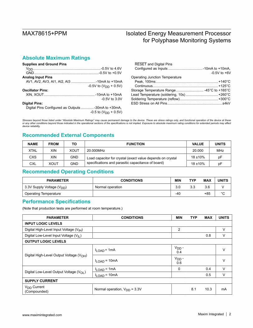
Supplies and Ground Pins VDD .....................................................................-0.5V to 4.6V GND ..................................................................-0.5V to +0.5V Analog Input Pins AV1, AV2, AV3, AI1, AI2, AI3 .........................-10mA to +10mA
-0.5V to (VDD + 0.5V)Oscillator Pins: XIN, XOUT .................................................... -10mA to +10mA
-0.5V to 3.0V Digital Pins: Digital Pins Configured as Outputs ............. -30mA to +30mA, -0.5 to (VDD + 0.5V)
RESET and Digital Pins Configured as Inputs ................................... -10mA to +10mA,
-0.5V to +6VOperating Junction Temperature Peak, 100ms ................................................................+140°C Continuous...................................................................+125°CStorage Temperature Range ............................ -45°C to +165°CLead Temperature (soldering, 10s) .................................+260°CSoldering Temperature (reflow) .......................................+300°CESD Stress on All Pins ........................................................±4kV
(Note that production tests are performed at room temperature.)
PARAMETER CONDITIONS MIN TYP MAX UNITSINPUT LOGIC LEVELSDigital High-Level Input Voltage (VIH) 2 V
Digital Low-Level Input Voltage (VIL) 0.8 V
OUTPUT LOGIC LEVELS
Digital High-Level Output Voltage (VOH)ILOAD = 1mA VDD -
0.4 V
ILOAD = 10mA VDD - 0.6 V
Digital Low-Level Output Voltage (VOL)ILOAD = 1mA 0 0.4 V
ILOAD = 10mA 0.5 V
SUPPLY CURRENTVDD Current(Compounded) Normal operation, VDD = 3.3V 8.1 10.3 mA
NAME FROM TO FUNCTION VALUE UNITS
XTAL XIN XOUT 20.000MHz 20.000 MHz
CXS XIN GND Load capacitor for crystal (exact value depends on crystal specifications and parasitic capacitance of board)
18 ±10% pF
CXL XOUT GND 18 ±10% pF
PARAMETER CONDITIONS MIN TYP MAX UNITS
3.3V Supply Voltage (VDD) Normal operation 3.0 3.3 3.6 V
Operating Temperature -40 +85 °C
MAX78615+PPM Isolated Energy Measurement Processor for Polyphase Monitoring Systems
www.maximintegrated.com Maxim Integrated 2
Absolute Maximum Ratings
Stresses beyond those listed under “Absolute Maximum Ratings” may cause permanent damage to the device. These are stress ratings only, and functional operation of the device at these or any other conditions beyond those indicated in the operational sections of the specifications is not implied. Exposure to absolute maximum rating conditions for extended periods may affect device reliability.
Performance Specifications
Recommended External Components
Recommended Operating Conditions

(Note that production tests are performed at room temperature.)
Note 1: Guaranteed by design, not subject to test.Note 2: Dependent on bus capacitance.
PARAMETER CONDITIONS MIN TYP MAX UNITSCRYSTAL OSCILLATORXIN to XOUT Capacitance (Note 1) 3 pF
Capacitance to GND (Note 1)XIN 5
pFXOUT 5
INTERNAL RC OSCILLATORNominal Frequency 20.000 MHz
Accuracy VDD = 3.0V, 3.6V; TA = 22°C ±1.5 %
RESET PINReset Pulse Fall Time (Note 1) 1 µs
Reset Pulse Width (Note 1) 5 µs
SPI SLAVE PORT (Figure 1)SCK Cycle Time (tSPICYC) 1 µs
Enable Lead Time (tSPILEAD) 15 ns
Enable Lag Time (tSPILAG) 0 ns
SCK Pulse Width (tSPIW)High 250
nsLow 250
SSB to First SCK Fall (tSPISCK) Ignore if SCK is low when SSB falls (Note 1) 2 ns
Disable Time (tSPIDIS) (Note 1) 0 ns
SCK to Data Out (SDO) (tSPIEV) 25 ns
Data Input Setup Time (SDI) (tSPISU) 10 ns
Data Input Hold Time (SDI) (tSPIH) 5 ns
I2C SLAVE PORT (Figure 2, Note 1)Bus Idle (Free) Time Between Transmissions (STOP/START) (tBUF) 1500 ns
I2C Input Fall Time (tICF) (Note 2) 20 300 ns
I2C Input Rise Time (tICR) (Note 2) 20 300 ns
I2C START or Repeated START Condition Hold Time (tSTH) 500 ns
I2C START or Repeated START Condition Setup Time (tSTS) 600 ns
I2C Clock High Time (tSCH) 600 ns
I2C Clock Low Time (tSCL) 1300 ns
I2C Serial Data Setup Time (tSDS) 100 ns
I2C Serial Data Hold Time (tSDH) 10 ns
I2C Valid Data Time (tVDA):SCL Low to SDA Output Valid ACK Signal from SCL Low to SDA (Out) Low
900 ns
MAX78615+PPM Isolated Energy Measurement Processor for Polyphase Monitoring Systems
www.maximintegrated.com Maxim Integrated 3
Performance Specifications (continued)
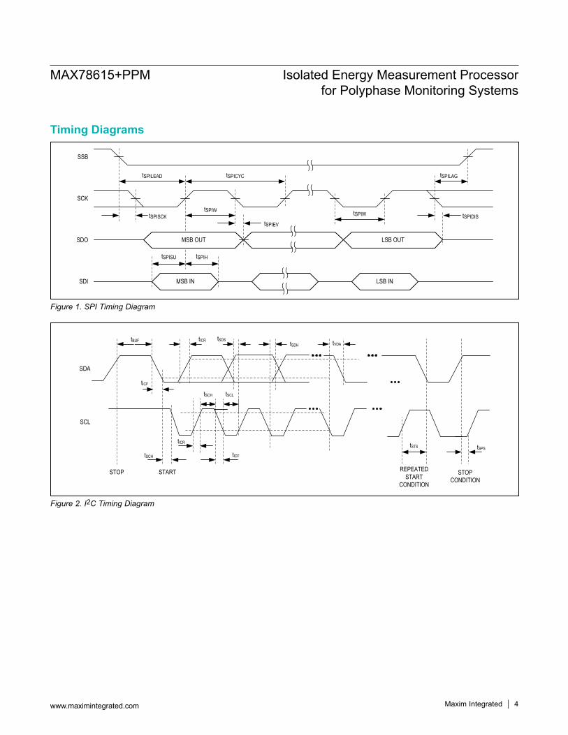
Figure 1. SPI Timing Diagram
Figure 2. I2C Timing Diagram
MSB OUT LSB OUT
MSB IN LSB IN
SSB
SCK
SDI
SDO
tSPILEAD tSPICYC
tSPIW tSPIW tSPIDIStSPIEV
tSPISU tSPIH
tSPISCK
tSPILAG
SCL
SDA
tBUF
STOP
tICR
tSCH tSCL
tICF
tICR
tICF
tSDStSDH tVDA
tSPStSTS
STOPCONDITION
REPEATED START
CONDITION
tSCH
START
MAX78615+PPM Isolated Energy Measurement Processor for Polyphase Monitoring Systems
www.maximintegrated.com Maxim Integrated 4
Timing Diagrams
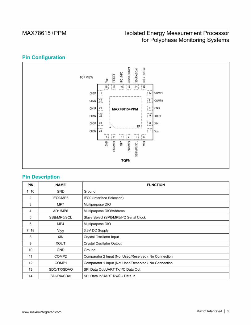
PIN NAME FUNCTION
1, 10 GND Ground
2 IFC0/MP8 IFC0 (Interface Selection)
3 MP7 Multipurpose DIO
4 AD1/MP6 Multipurpose DIO/Address
5 SSB/MP5/SCL Slave Select (SPI)/MP5/I2C Serial Clock
6 MP4 Multipurpose DIO
7, 18 VDD 3.3V DC Supply
8 XIN Crystal Oscillator Input
9 XOUT Crystal Oscillator Output
10 GND Ground
11 COMP2 Comparator 2 Input (Not Used/Reserved), No Connection
12 COMP1 Comparator 1 Input (Not Used/Reserved), No Connection
13 SDO/TX/SDAO SPI Data Out/UART Tx/I2C Data Out
14 SDI/RX/SDAI SPI Data In/UART Rx/I2C Data In
IFC0
/MP8
AD1/M
P6
SSB/
MP5/S
CL MP4
GND
RESET
SCK/
AD0/M
P1
SDI/R
X/SD
AI
V DD
SDO/
TX/S
DA0
CH1N
CH3P
CH3N
GND
XOUT
XIN
VDD
MP7
IFC1
/MP0
CH1P
COMP2CH2N
COMP1CH2P
TQFN
TOP VIEW
+
131415161718
12
11
10
9
8
7
19
20
21
22
23
24
654321
MAX78615+PPM
EP
MAX78615+PPM Isolated Energy Measurement Processor for Polyphase Monitoring Systems
www.maximintegrated.com Maxim Integrated 5
Pin Configuration
Pin Description

PIN NAME FUNCTION
15 SCK/AD0/MP1 SPI Clock/Address
16 IFC1/MP0 Multipurpose DIO/Interface Selection
17 RESET Active-Low Reset Input
19 CH2P Pulse Transformer Interface Channel 2 (Negative)
20 CH2N Pulse Transformer Interface Channel 2 (Positive)
21 CH1P Pulse Transformer Interface Channel 1 (Negative)
22 CH1N Pulse Transformer Interface Channel 1 (Positive)
23 CH3P Pulse Transformer Interface Channel 3 (Negative)
24 CH3N Pulse Transformer Interface Channel 3 (Positive)
— EP Exposed Pad. Internally connected to GND. Not intended as an electrical connection point.
NAME DESCRIPTION
AFE Analog Front-End
ADC Analog-to-Digital Converter
FSV Peak System Voltage Required to Produce 250mVpk at the AFE ADC
FSI Peak System Current Required to Produce 250mVpk at the AFE ADC
FSP Full-Scale Power (FSI x FSV)
SPS Sample Per Second
HPF Highpass Filter
MAX78615+PPM Isolated Energy Measurement Processor for Polyphase Monitoring Systems
www.maximintegrated.com Maxim Integrated 6
Pin Description (continued)
Glossary
IOMUX
INFOBLOCK
FLASH4Kx16
PROGRAMMEMORY
RAM512x24
PULSE TRANSFORMER INTERFACES
PULSE TRANSFORMER CONTROL
2.5VREG
XTALOSC
CLKSEL
CLKGEN
EMP
TIMERSWATCHDOG
RCOSC
VCC
XOUT
XIN
GND
RESET
IFC0/MP8
IFC1/MP0
SCK/AD0/MP1
SDI / RX / SDAI
SDO / TX / SDAO
MP4
SSB/MP5/SCL
AD1/MP6
MP7
COMP1
COMP2
VDD CH3P CH3N CH1P CH1N CH2P CH2N GND
SPI
I2C
UART
MAX78615+PPM
MAX78615+PPM Isolated Energy Measurement Processor for Polyphase Monitoring Systems
www.maximintegrated.com Maxim Integrated 7
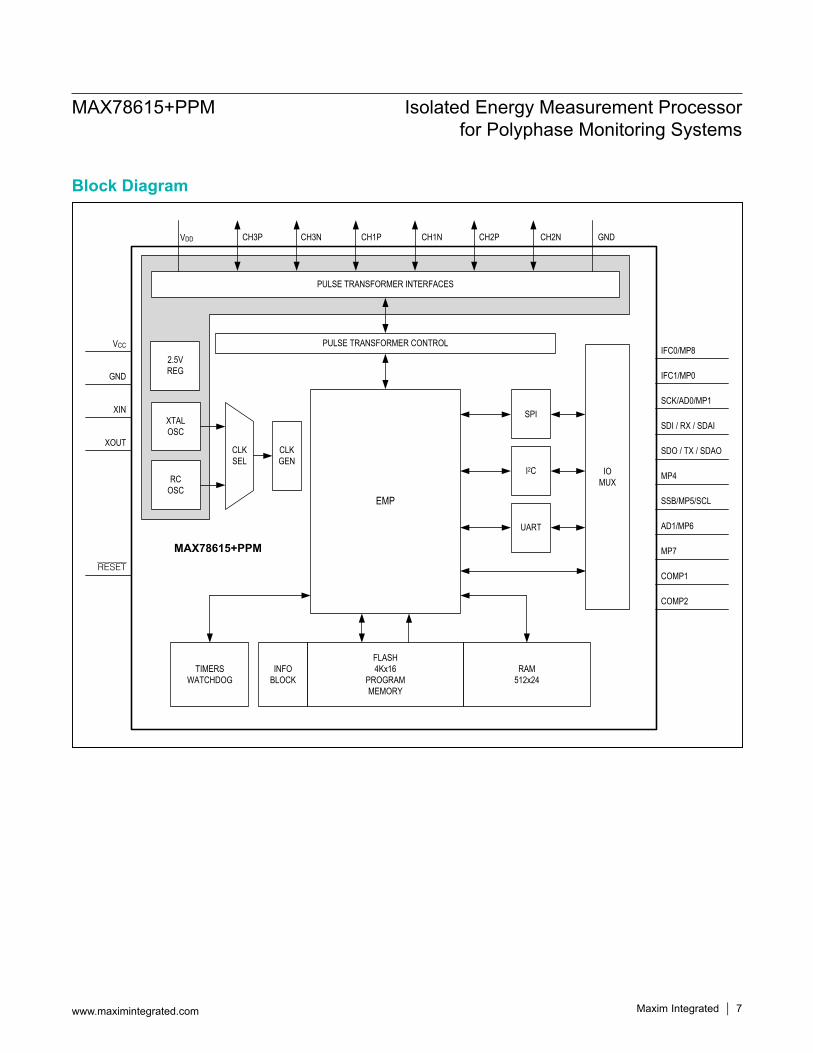
Block Diagram

On-Chip Resources OverviewThe MAX78615+PPM device integrates all the hardware blocks required for accurate AC power and energy mea-surement. Included on the device are the following:
Oscillator and clock management logic Power-on reset, watchdog timer, and reset circuitry 24-bit measurement processor with RAM and flash
memory UART, SPI, and I2C serial communication interfaces
and multipurpose digital I/O Pulse transformer interfaces (for connection to up to
three or more MAX78700 or MAX71071 devices)
Clock ManagementThe device can be clocked by oscillator circuitry that relies on an external crystal or, as a backup source, by a trimmed internal RC oscillator. The internal RC oscillator provides an accurate clock source for UART baud rate generation.The chip hardware automatically handles the clock sources logic and distributes the clock to the rest of the device. Upon reset or power-on, the device will utilize the internal RC oscillator circuit for the first 1024 clock cycles, allowing the external crystal adequate time to startup. The device will then automatically select the external clock, if available. It will also automatically switch back to the internal oscillator in the event of a failure with the external oscillator. This condition is also monitored by the proces-sor and available to the user in the STATUS register. The MAX78615+PPM external clock circuitry requires a 20.000MHz crystal. The circuitry includes two 18pF ceramic capacitors. Figure 3 shows the typical connection of the external crystal. This oscillator is self-biasing and therefore an external resistor should not be connected across the crystal. An external 20MHz system clock signal can also be uti-lized instead of the crystal. In this case, the external clock should be connected to the XOUT pin while the XIN pin should be connected to GND. Alternatively, if no external crystal or clock is utilized, the XOUT pin should be connected to GND and the XIN pin left unconnected.
Power-On Reset, Watchdog-Timer, and Reset CircuitryPower-On Reset (POR)An on-chip power-on reset (POR) block monitors the supply voltage (VDD) and initializes the internal digital circuitry at power-on. Once VDD is above the minimum operating threshold, the POR circuit triggers and initi-ates a reset sequence. It also issues a reset to the digital circuitry if the supply voltage falls below the minimum operating level.
Watchdog Timer (WDT)A watchdog timer (WDT) block detects any software processing errors. The embedded software periodically refreshes the free-running watchdog timer to prevent it from timing out. If the WDT times out, it is an indication that software is no longer being executed in the intended sequence; thus, a system reset is initiated.
External Reset Pin (RESET Pin) In addition to the internal sources, a reset can be forced by applying a low level to the RESET pin. If the RESET pin is pulled low, all digital activities in the device stop, except the clock management circuitry and oscillators, which continue to run. The external reset input is filtered to prevent spurious reset events in noisy environments. The reset does not occur until RESET has been held low for at least 1µs.Once initiated, the reset mode persists until the RESET is set high and the reset timer times out (4096 clock cycles). At the completion of the reset sequence, the internal reset is released and the processor begins executing from address 0.If not used, the RESET pin can be connected either directly or through a pullup resistor to VDD supply. Figure 4 shows simple connection diagram examples.
Figure 3. Typical Connection of External Crystal
MAX78615+PPM20MHz
18pF
18pF
XIN
XOUT
MAX78615+PPM Isolated Energy Measurement Processor for Polyphase Monitoring Systems
www.maximintegrated.com Maxim Integrated 8

24-Bit Measurement Processor The MAX78615+PPM integrates a fixed-point 24-bit signal processor that performs all the digital signal pro-cessing necessary for energy measurement, alarm gen-eration, calibration, compensation, etc. Functionality and operation of the device is determined by the firmware and described in the Functional Description and Operation section.
Flash and RAMThe MAX78615+PPM includes 8KB of on-chip flash memory. The flash memory contains program code and is used to stores coefficients, calibration data, and con-figuration settings. The MAX78615+PPM includes 1.5KB of on-chip RAM, which contains the values of input and output registers and is utilized by the firmware for its operations.
Digital I/O PinsThere are a total of nine digital input/outputs on the MAX78615+PPM device. Some are dedicated to serial interface communications and configuration. Others are multi-purpose I/O (indicated as MP or “Multi-Purpose” pins) that can be used as a simple output under user control or routed to special purpose internal signals, such as alarm signaling.
Communication InterfacesThe MAX78615+PPM includes three communication interface options: UART, SPI, and I2C. Since the I/O pins are shared, only one mode is supported at a time. Interface configuration pins are sampled at power-on or reset to determine which interface is active.
Isolated Analog Front-End (AFE)Up to three isolation interfaces (channels) are provided to provide power, configure/control, and read measure-ment data from a MAX78700 or MAX71071. The power is provided by the MAX78615+PPM, through dedicated pulses that are spaced at 10.00MHz/6 (600ns period), with write and read pulses located in between. The power pulses are also used to provide the synchronization for the MAX78700 (or MAX71071) on-chip PLL. Within every power pulse cycle a write data pulse and a read data pulse is inserted.Data sent from the MAX78615+PPM to the isolated AFE:
Power ADC Configuration Control
Data sent from the isolated AFE to the MAX78615+PPM: Voltage Samples Current Samples Die Temperature Bandgap and Trim Information
Figure 4. Connection Examples for RESET Pin
MAX78615+PPM
V3P3D
RESET
GNDD
10kΩ
1nF
GND
V3P3
MANUAL RESET SWITCH
A) RESET EXTERNAL CONNECTION EXAMPLE
MAX78615+PPM
V3P3D
RESET
GNDD
GND
V3P3
B) UNUSED RESET CONNECTION EXAMPLE
MAX78615+PPM Isolated Energy Measurement Processor for Polyphase Monitoring Systems
www.maximintegrated.com Maxim Integrated 9
Functional Description and OperationThis section describes the MAX78615+PPM functional-ity. It includes measurements and relevant calculations, alarms, auxiliary functions such as calibrations, zero-crossing, etc.A set of input (write), output (read), and read/write regis-ters are provided to allow access to calculated data and alarms and to configure the device. The input (write) regis-ters values can be saved into flash memory through a spe-cific command. The values saved into flash memory are loaded in these registers at reset or power-on as defaults.
Signal Processing DescriptionAFE ConfigurationThe MAX78615+PPM supplies configuration and control to the isolated AFEs. The MAX71071 and MAX78700 have different configurations to support the same solution.
Input MappingUp to three remotes can be connected to the remote inter-faces. The sensors are expected by the firmware to be connected to support the logical current/voltage mapping as shown in Table 2.
Highpass Filters and Offset RemovalOffset registers for each analog input contain values to be subtracted from the raw ADC outputs for the purpose of removing inherent system DC offsets from any cal-culated power and RMS values. When the integrated highpass filter (HPF) is enabled, it dynamically updates the offset registers every accumulation interval. During each accumulation interval (or low-rate cycle), the HPF calculates the median or DC average of each input. Adjustable coefficients determine what portion of the measured offset is combined with the previous offset value (see Table 3).The HPF_COEF_I and HPF_COEF_V registers contain signed fixed point numbers with a usable range of 0 to 1.0-LSB (negative values are not supported). Setting them to 1.0 (0x7FFFFF) causes the entire measured offset to be applied to the offset register enabling lump-sum offset removal. Setting them to zero disables any dynamic update of the offset registers by the HPF. The HPF coefficients apply to all three channels (current or voltage).
Table 1. Sample Rate and Preamplifier Settings
Table 4. Highpass Filter Coefficients
Table 2. Analog Input Assignment Table 3. Offset Registers
*Sample rate per channel on multiplexed ADC.**Sample rate per channel with one ADC per channel.
PARAMETER MAX78700 MAX71071 NOTES
SPS 3306.9* 2381** Samples per second
ADC PREAMP 1x 9x —
REMOTE ANALOG INPUT PINS
REMOTE INTERFACE INPUT NAME
INAP/NCH1
Voltage 1 (AV1)
INBP/N Current 1 (AI1)
INAP/NCH2
Voltage 2 (AV2)
INBP/N Current 2 (AI2)
INAP/NCH3
Voltage 3 (AV3)
INBP/N Current 3 (AI3)
REGISTER DESCRIPTION
V1_OFFS Voltage Input AV1 Offset Calibration
V2_ OFFS Voltage Input AV2 Offset Calibration
V3_ OFFS Voltage Input AV3 Offset Calibration
I1_OFFS Current Input AI1 Offset Calibration
I2_ OFFS Current Input AI2 Offset Calibration
I3_ OFFS Current Input AI3 Offset Calibration
REGISTER DESCRIPTION
HPF_COEF_I HPF Coefficient for AIA, AIB, and AIC Current Inputs
HPF_COEF_V HPF Coefficient for AVA, AVB, and AVC Voltage Inputs
MAX78615+PPM Isolated Energy Measurement Processor for Polyphase Monitoring Systems
www.maximintegrated.com Maxim Integrated 10
Gain CorrectionThe system (sensors) and the MAX78615+PPM device inherently have gain errors that can be corrected by using the gain registers. These registers can be directly accessed and modified by an external host processor or automati-cally updated by an integrated self-calibration routine.Input gain registers are signed fixed-point numbers with the binary point to the left of bit 21. They are set to 1.0 by default and have a usable range of 0 to 4.0-LSB (nega-tive values are not supported). The gain equation for each input X can be described as Y = gain * X.
Die Temperature Compensation The MAX78615+PPM receives the isolated ADC (MAX78700 or MAX71071) die temperature measurements. This data is used by the signal processor for correcting the voltage ref-erence error (bandgap curvature). It is also available to the user in the TEMPC registers. Temperature data has a fixed scaling with a range of -16384°C to +16384°C less one LSB (format S.10). See Table 6.Setting the temperature compensation (TC) bit in the Control register allows the firmware to further adjust the system gain based on measured isolated die tempera-ture. The isolated ADC die temperature offset is typically calibrated by the user during the calibration stage. Die temperature gain is set to a factory default value for most applications, but can be adjusted by the user. See Table 7.
Phase CompensationPhase compensation registers are used to compensate for phase errors or time delays between the voltage input source and respective current source that are introduced by the off-chip sensor circuit. The user configurable regis-ters are signed fixed point numbers with the binary point to the left of bit 21. Values are in units of high rate sample delays so each integer unit of delay is 1/SPS with a total possible delay of ±4 samples. See Table 8.Example:To compensate a phase error of 315µs (or 6.8° at 60Hz) for a MAX78700 isolated AFE it is necessary to set the relevant phase compensation register as follows:
6Phase Error 315 ECompensation1 1
Sample Rate 3174.6Compensation 1.0000
−= =
=
The value to enter in the phase compensation register is therefore:
621315 EPHASECOMP x 2 2097150 0x1FFFFD
13174.6
−= = =
Table 5. Voltage and Current Gain Registers Table 7. Remote ADC Temperature Calibration Registers
Table 8. Phase Compensation Registers
Table 6. Remote ADC Die Temperature Registers
REGISTER DESCRIPTION
V1_GAIN Voltage Input AV1 Gain Calibration
V2_GAIN Voltage Input AV2 Gain Calibration
V3_GAIN Voltage Input AV3 Gain Calibration
I1_GAIN Current Input AI1 Gain Calibration
I2_GAIN Current Input AI2 Gain Calibration
I3_GAIN Current Input AI3 Gain Calibration
REGISTER DESCRIPTION LSB TIME SCALE
TEMPC1 Chip Temperature (Celsius°) Channel 1 °C/210
1 intervalTEMPC2 Chip Temperature (Celsius°) Channel 2 °C/210
TEMPC3 Chip Temperature (Celsius°) Channel 3 °C/210
REGISTER DESCRIPTION
T_OFFS1, TOFFS2, TOFFS3
Die Temperature Offset Calibration.
T_GAIN Die Temperature Slope Calibration, set by factory.
REGISTER LSB DESCRIPTION
PHASECOMP1 SAMPLE/221Phase (delay) compensation for AI1 relative to AV1
PHASECOMP2 SAMPLE/221Phase (delay) compensation for AI2 relative to AV1
PHASECOMP3 SAMPLE/221Phase (delay) compensation for AI3 relative to AV1
MAX78615+PPM Isolated Energy Measurement Processor for Polyphase Monitoring Systems
www.maximintegrated.com Maxim Integrated 11
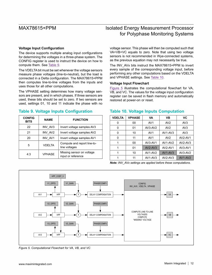
Voltage Input ConfigurationThe device supports multiple analog input configurations for determining the voltages in a three-phase system. The CONFIG register is used to instruct the device on how to compute them. See Table 9.The VDELTA bit must be set whenever the voltage sensors measure phase voltages (line-to-neutral), but the load is connected in a Delta configuration. The MAX78615+PPM then computes line-to-line voltages from the inputs and uses those for all other computations.The VPHASE setting determines how many voltage sen-sors are present, and in which phases. If three sensors are used, these bits should be set to zero. If two sensors are used, settings 01, 10 and 11 indicate the phase with no
voltage sensor. This phase will then be computed such that VA+VB+VC equals to zero. Note that using two voltage sensors is not recommended in Wye-connected systems, as the previous equation may not necessarily be true.The INV_AVx bits instruct the MAX78615+PPM to invert every sample of the corresponding voltage input, before performing any other computations based on the VDELTA and VPHASE settings. See Table 10.
Voltage Input FlowchartFigure 5 illustrates the computational flowchart for VA, VB, and VC. The values for the voltage input configuration register can be saved in flash memory and automatically restored at power-on or reset.
Table 9. Voltage Inputs Configuration Table 10. Voltage Inputs Computation
Note: INV_AVx settings are applied before these computations.
CONFIG BITS NAME FUNCTION
22 INV_AV3 Invert voltage samples AV3
21 INV_AV2 Invert voltage samples AV2
20 INV_AV1 Invert voltage samples AV1
5 VDELTA Compute and report line-to-line voltages
4:3 VPHASE Missing sensor on voltage input or reference
VDELTA VPHASE VA VB VC0 00 AV1 AV2 AV3
0 01 AV3-AV2 AV2 AV3
0 10 AV1 AV1-AV3 AV3
0 11 AV1 AV2 AV2-AV1
1 00 AV3-AV1 AV1-AV2 AV2-AV3
1 01 AV2-AV3 AV2-AV1 AV3-AV1
1 10 AV1-AV2 AV1-AV3 AV3-AV2
1 11 AV1-AV3 AV2-AV3 AV1-AV2
Figure 5. Computational Flowchart for VA, VB, and VC
DELAY COMPENSATION VAAV1
VB
VC
V1_GAIN
HPF_COEF_V
X
V1_OFFS
HPF
PHASECOMP1
COMPUTE LINE-TO-LINEVOLTAGESCOMPUTE
“MISSING” VOLTAGE
CONFIG:INV_AVX , VDELTA , VPHASE
DELAY COMPENSATIONAV2
V2_GAIN
X
V2_OFFS
HPF
PHASECOMP2
DELAY COMPENSATIONAV3
V3_GAIN
X
V3_OFFS
HPF
PHASECOMP3
MAX78615+PPM Isolated Energy Measurement Processor for Polyphase Monitoring Systems
www.maximintegrated.com Maxim Integrated 12
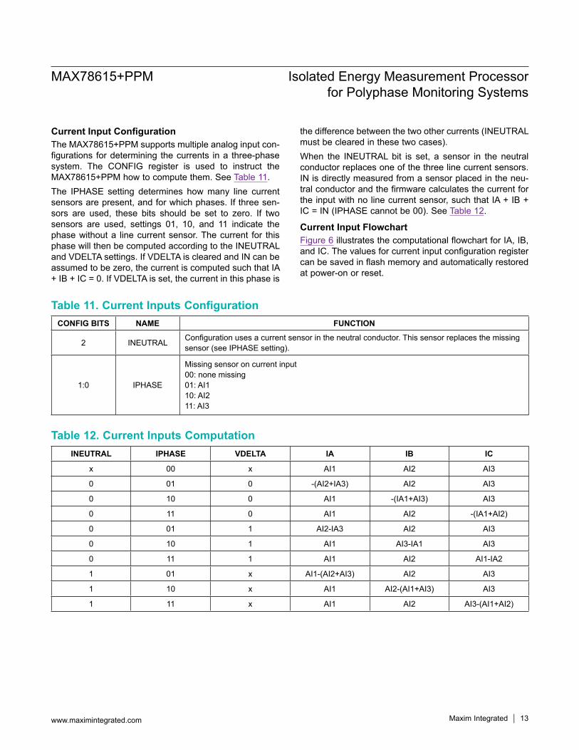
Current Input ConfigurationThe MAX78615+PPM supports multiple analog input con-figurations for determining the currents in a three-phase system. The CONFIG register is used to instruct the MAX78615+PPM how to compute them. See Table 11.The IPHASE setting determines how many line current sensors are present, and for which phases. If three sen-sors are used, these bits should be set to zero. If two sensors are used, settings 01, 10, and 11 indicate the phase without a line current sensor. The current for this phase will then be computed according to the INEUTRAL and VDELTA settings. If VDELTA is cleared and IN can be assumed to be zero, the current is computed such that IA + IB + IC = 0. If VDELTA is set, the current in this phase is
the difference between the two other currents (INEUTRAL must be cleared in these two cases). When the INEUTRAL bit is set, a sensor in the neutral conductor replaces one of the three line current sensors. IN is directly measured from a sensor placed in the neu-tral conductor and the firmware calculates the current for the input with no line current sensor, such that IA + IB + IC = IN (IPHASE cannot be 00). See Table 12.
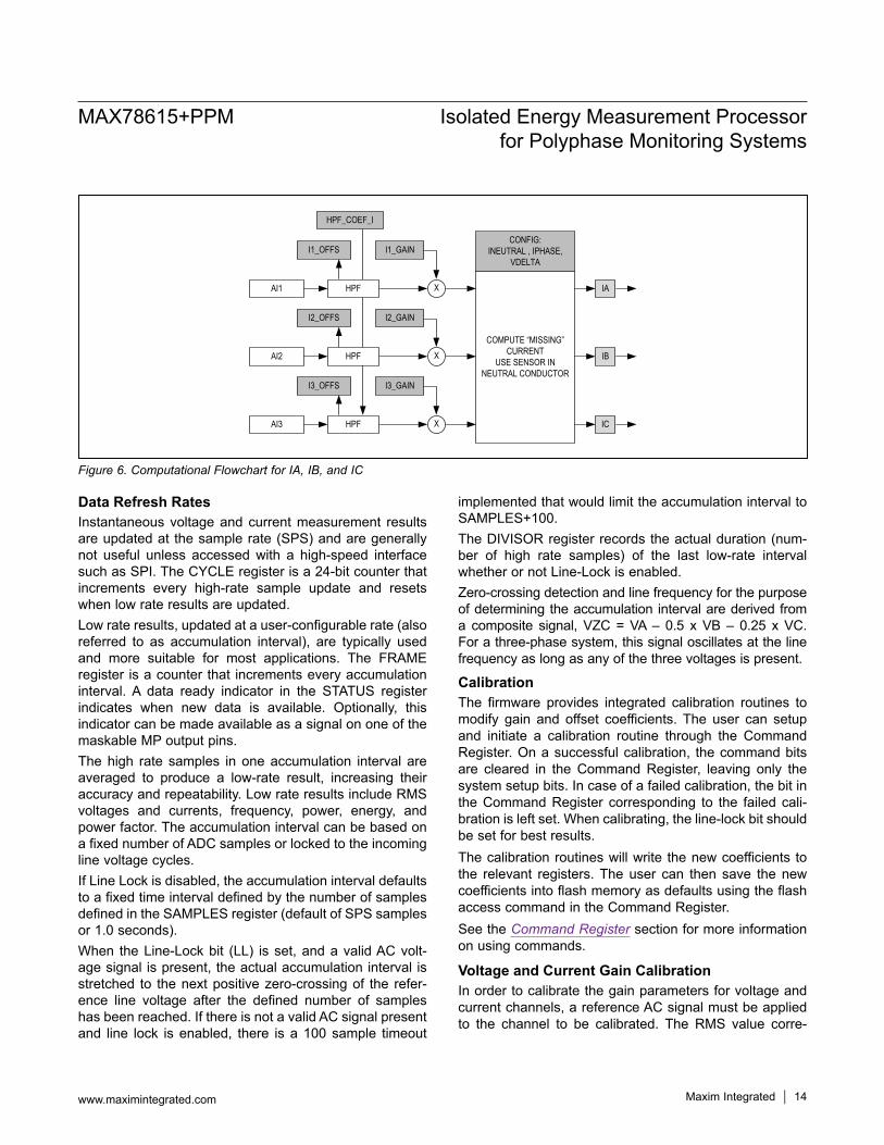
Current Input FlowchartFigure 6 illustrates the computational flowchart for IA, IB, and IC. The values for current input configuration register can be saved in flash memory and automatically restored at power-on or reset.
Table 11. Current Inputs Configuration
Table 12. Current Inputs Computation
CONFIG BITS NAME FUNCTION
2 INEUTRAL Configuration uses a current sensor in the neutral conductor. This sensor replaces the missing sensor (see IPHASE setting).
1:0 IPHASE
Missing sensor on current input00: none missing01: AI110: AI211: AI3
INEUTRAL IPHASE VDELTA IA IB IC
x 00 x AI1 AI2 AI3
0 01 0 -(AI2+IA3) AI2 AI3
0 10 0 AI1 -(IA1+AI3) AI3
0 11 0 AI1 AI2 -(IA1+AI2)
0 01 1 AI2-IA3 AI2 AI3
0 10 1 AI1 AI3-IA1 AI3
0 11 1 AI1 AI2 AI1-IA2
1 01 x AI1-(AI2+AI3) AI2 AI3
1 10 x AI1 AI2-(AI1+AI3) AI3
1 11 x AI1 AI2 AI3-(AI1+AI2)
MAX78615+PPM Isolated Energy Measurement Processor for Polyphase Monitoring Systems
www.maximintegrated.com Maxim Integrated 13
Data Refresh RatesInstantaneous voltage and current measurement results are updated at the sample rate (SPS) and are generally not useful unless accessed with a high-speed interface such as SPI. The CYCLE register is a 24-bit counter that increments every high-rate sample update and resets when low rate results are updated.Low rate results, updated at a user-configurable rate (also referred to as accumulation interval), are typically used and more suitable for most applications. The FRAME register is a counter that increments every accumulation interval. A data ready indicator in the STATUS register indicates when new data is available. Optionally, this indicator can be made available as a signal on one of the maskable MP output pins.The high rate samples in one accumulation interval are averaged to produce a low-rate result, increasing their accuracy and repeatability. Low rate results include RMS voltages and currents, frequency, power, energy, and power factor. The accumulation interval can be based on a fixed number of ADC samples or locked to the incoming line voltage cycles.If Line Lock is disabled, the accumulation interval defaults to a fixed time interval defined by the number of samples defined in the SAMPLES register (default of SPS samples or 1.0 seconds).When the Line-Lock bit (LL) is set, and a valid AC volt-age signal is present, the actual accumulation interval is stretched to the next positive zero-crossing of the refer-ence line voltage after the defined number of samples has been reached. If there is not a valid AC signal present and line lock is enabled, there is a 100 sample timeout
implemented that would limit the accumulation interval to SAMPLES+100.The DIVISOR register records the actual duration (num-ber of high rate samples) of the last low-rate interval whether or not Line-Lock is enabled.Zero-crossing detection and line frequency for the purpose of determining the accumulation interval are derived from a composite signal, VZC = VA – 0.5 x VB – 0.25 x VC. For a three-phase system, this signal oscillates at the line frequency as long as any of the three voltages is present.
CalibrationThe firmware provides integrated calibration routines to modify gain and offset coefficients. The user can setup and initiate a calibration routine through the Command Register. On a successful calibration, the command bits are cleared in the Command Register, leaving only the system setup bits. In case of a failed calibration, the bit in the Command Register corresponding to the failed cali-bration is left set. When calibrating, the line-lock bit should be set for best results.The calibration routines will write the new coefficients to the relevant registers. The user can then save the new coefficients into flash memory as defaults using the flash access command in the Command Register.See the Command Register section for more information on using commands.
Voltage and Current Gain CalibrationIn order to calibrate the gain parameters for voltage and current channels, a reference AC signal must be applied to the channel to be calibrated. The RMS value corre-
Figure 6. Computational Flowchart for IA, IB, and IC
AI1
I1_GAIN
HPF_COEF_I
X
I1_OFFS
HPF
COMPUTE “MISSING” CURRENT
USE SENSOR IN NEUTRAL CONDUCTOR
CONFIG:INEUTRAL , IPHASE,
VDELTA
AI2
I2_GAIN
X
I2_OFFS
HPF
AI3
I3_GAIN
X
I3_OFFS
HPF
IA
IB
IC
Isolated Energy Measurement Processor for Polyphase Monitoring Systems
www.maximintegrated.com Maxim Integrated 14
MAX78615+PPM
sponding to the applied reference signal must be entered in the relevant target register (V_TARGET, I_TARGET). Considering calibration is done with low rate RMS results, the value of the target register should never be set to a value above 70.7% of full scale.Initially, the value of the gain is set to unity for the selected channels. RMS values are then calculated on all inputs and averaged over the number of measurement cycles set by the CALCYCS register. The new gain is calculated by dividing the appropriate Target register value by the averaged measured value. The new gain is then written to the select Gain registers unless an error occurred.Note that there is only one V_TARGET register for voltag-es. It is possible to calibrate multiple or all voltage chan-nels simultaneously, if and only if the same RMS voltage value is applied to each corresponding input. Analogous considerations apply to the current channels, which are calibrated via the I_TARGET register.
Offset CalibrationIf the highpass filters are not desired then the user can fix the DC offset compensation registers through calibration. To calibrate offset, all signals should be removed from all analog inputs although it is possible to do the calibration in the presence of AC signals. In the command, the user also specifies which channel(s) to calibrate. Target regis-ters are not used for offset calibration.
During the calibration process, each input is accumu-lated over the entire calibration interval as specified by the CALCYCS register. The result is divided by the total number of samples and written to the appropriate offset register, if selected in the calibration command. Using the offset calibration command sets the respective HPF coef-ficients to zero, thereby fixing the offset registers to their calibrated values.
Die Temperature CalibrationTo re-calibrate the on-chip temperature sensor offset, the user must first write the known chip temperature to the T_TARGET register. Next, the user initiates the Temperature Calibration Command in the Command Register. This will update the T_OFFS offset parameter with a new offset based on the known temperature sup-plied by the user. The T_GAIN gain register is set by the factory and not updated with this routine.
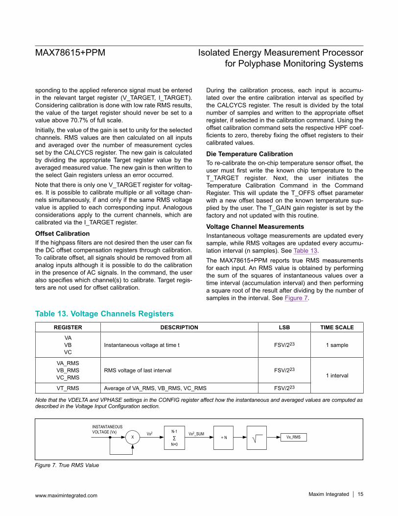
Voltage Channel MeasurementsInstantaneous voltage measurements are updated every sample, while RMS voltages are updated every accumu-lation interval (n samples). See Table 13.The MAX78615+PPM reports true RMS measurements for each input. An RMS value is obtained by performing the sum of the squares of instantaneous values over a time interval (accumulation interval) and then performing a square root of the result after dividing by the number of samples in the interval. See Figure 7.
Table 13. Voltage Channels Registers
Note that the VDELTA and VPHASE settings in the CONFIG register affect how the instantaneous and averaged values are computed as described in the Voltage Input Configuration section.
REGISTER DESCRIPTION LSB TIME SCALE
VAVBVC
Instantaneous voltage at time t FSV/223 1 sample
VA_RMSVB_RMSVC_RMS
RMS voltage of last interval FSV/2231 interval
VT_RMS Average of VA_RMS, VB_RMS, VC_RMS FSV/223
Figure 7. True RMS Value
Vx2Vx_RMS ÷ N
INSTANTANEOUS VOLTAGE (Vx) N-1
∑N=0
XVx2_SUM
MAX78615+PPM Isolated Energy Measurement Processor for Polyphase Monitoring Systems
www.maximintegrated.com Maxim Integrated 15
Line Frequency This output is a measurement of the fundamental fre-quency of the AC voltage source. It is derived from a composite signal and therefore applies to all three phases (it is a single reading per device) and is updated every 64 line cycles. Frequency data is reported as binary fixed-point number, with a range of 0 to +256Hz less one LSB (format S.16). See Table 14.
Current Channel MeasurementsInstantaneous current measurements are updated every sample, while peak currents and RMS currents are updat-ed every accumulation interval (n samples). See Table 15.Note that the INEUTRAL and IPHASE settings in the CONFIG register affect how the instantaneous and aver-aged values are computed as described in the Current Input Configuration section.
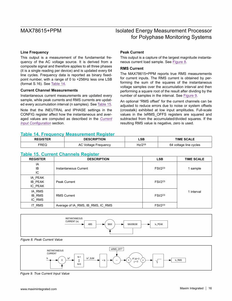
Peak Current This output is a capture of the largest magnitude instanta-neous current load sample. See Figure 8.
RMS CurrentThe MAX78615+PPM reports true RMS measurements for current inputs. The RMS current is obtained by per-forming the sum of the squares of the instantaneous voltage samples over the accumulation interval and then performing a square root of the result after dividing by the number of samples in the interval. See Figure 9.An optional “RMS offset” for the current channels can be adjusted to reduce errors due to noise or system offsets (crosstalk) exhibited at low input amplitudes. Full-scale values in the IxRMS_OFFS registers are squared and subtracted from the accumulated/divided squares. If the resulting RMS value is negative, zero is used.
Table 14. Frequency Measurement Register
Table 15. Current Channels Register
REGISTER DESCRIPTION LSB TIME SCALEFREQ AC Voltage Frequency Hz/216 64 voltage line cycles
REGISTER DESCRIPTION LSB TIME SCALEIAIBIC
Instantaneous Current FSI/223 1 sample
IA_PEAKIB_PEAKIC_PEAK
Peak Current FSI/223
1 intervalIA_RMSIB_RMSIC_RMS
RMS Current FSI/223
IT_RMS Average of IA_RMS, IB_RMS, IC_RMS FSI/223
Figure 8. Peak Current Value
Figure 9. True Current Input Value
INSTANTANEOUSCURRENT (Ix)
ABS MAX MAXIMUM Ix_PEAK
Ix Ix2Ix_RMS ÷ N
INSTANTANEOUSCURRENT
N-1∑
N=0X
Ix2_SUM— IF |x|< 0
y = 0x y
IxRMS_OFF2
MAX78615+PPM Isolated Energy Measurement Processor for Polyphase Monitoring Systems
Maxim Integrated 16www.maximintegrated.com

Current and Voltage ImbalanceImbalance of a three-phase system is typically defined as the percentage of the maximum deviation of any of the phases from the average of the phases.Voltage imbalance is obtained from Vx_RMS and VT_RMS as
max ( VARMS VTRMS ,
VBRMS VTRMS ,
VCRMS VTRMS )VIMBAL % x 100
VTRMS
−
−
−=
Current imbalance is obtained from Ix_RMS and IT_RMS as
max ( IARMS ITRMS ,
IBRMS ITRMS ,
ICRMS ITRMS )IIMBAL % x 100
ITRMS
−
−
−=
The MAX78615+PPM monitors the deviation of any phase from the average value. It generates an alarm if the devia-tion exceeds user programmable threshold; V_IMB_MAX for voltages and I_IMB_MAX for currents.
The thresholds are expressed as binary full-scale units with a value range of 0.0 to 1.0 less one LSB (S.23 for-mat). 1.0 thus corresponds to 100% imbalance.Example: generate an alarm if voltage imbalance exceeds 1.5%.
MAX23
IMB1.5
V int x 2 125.829 0x1E8b5100
= = =
Power CalculationsThis section describes the detailed flow of power calcula-tions in the MAX78615+PPM. Table 16 lists the available measurement results for AC power.
Active Power (P)The instantaneous power results (PA, PB, PC) are obtained by multiplying aligned instantaneous voltage and current samples. The sum of these results are then averaged over N samples (accumulation time) to compute the average active power (WATT_A, WATT_B, WATT_C). See Figure 10.The value in the Px_OFFS register is the “Power Offset” for the power calculations. Full-scale values in the Px_OFFS register are subtracted from the magnitude of the averaged active power. If the resulting active power value results in a sign change, zero watts are reported.
Table 16. Power and Power Factor Registers
Note that the voltage and current configuration settings in the CONFIG register affect the physical meaning of the computed power results.
REGISTER DESCRIPTION LSB TIME SCALE
WATT_AWATT_BWATT_C
Average Active Power (P) FSP/223
1 interval
VAR_AVAR_BVAR_C
Average Reactive Power (Q) FSP/223
VA_AVA_BVA_C
Apparent Power (S) FSP/223
PF_APF_BPF_C
Power Factor FSP/223
WATT_T Average of WATT_A, WATT_B, WATT_C FSP/223
VAR_T Average of VAR_A, VAR_B, VAR_C FSP/223
VA_T Average of VA_A, VA_B, VA_C FSP/223
PF_T Total power factor: Equal to WATT_T / VA_T FSP/223
MAX78615+PPM Isolated Energy Measurement Processor for Polyphase Monitoring Systems
www.maximintegrated.com Maxim Integrated 17
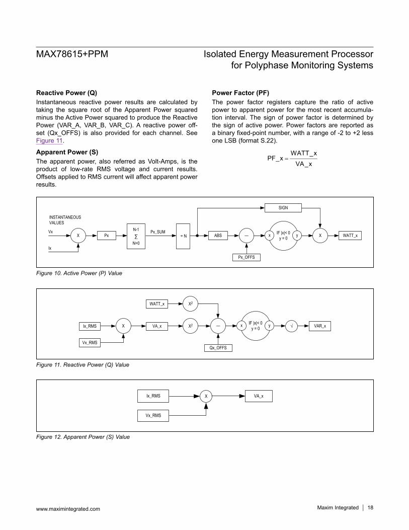
Reactive Power (Q)Instantaneous reactive power results are calculated by taking the square root of the Apparent Power squared minus the Active Power squared to produce the Reactive Power (VAR_A, VAR_B, VAR_C). A reactive power off-set (Qx_OFFS) is also provided for each channel. See Figure 11.
Apparent Power (S)The apparent power, also referred as Volt-Amps, is the product of low-rate RMS voltage and current results. Offsets applied to RMS current will affect apparent power results.
Power Factor (PF)The power factor registers capture the ratio of active power to apparent power for the most recent accumula-tion interval. The sign of power factor is determined by the sign of active power. Power factors are reported as a binary fixed-point number, with a range of -2 to +2 less one LSB (format S.22).
WATT_xPF_x
VA_x=
Figure 10. Active Power (P) Value
Figure 11. Reactive Power (Q) Value
Figure 12. Apparent Power (S) Value
Vx
INSTANTANEOUS VALUES
N-1∑
N=0X — IF |x|< 0
y = 0x y
Px_OFFS
Ix
Px ÷ NPx_SUM
ABS X WATT_x
SIGN
IF |x|< 0y = 0x yX VAR_x√Ix_RMS
Vx_RMS
VA_x X2
WATT_x X2
—
Qx_OFFS
XIx_RMS
Vx_RMS
VA_x
MAX78615+PPM Isolated Energy Measurement Processor for Polyphase Monitoring Systems
www.maximintegrated.com Maxim Integrated 18
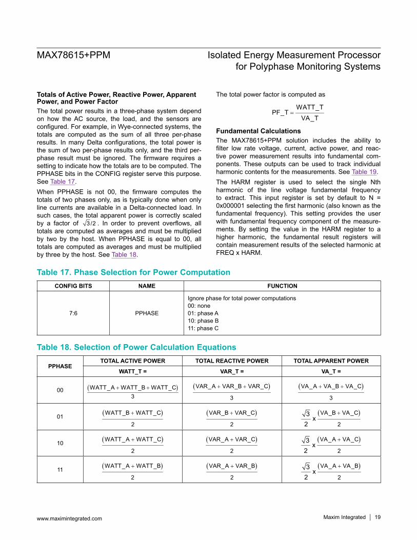
Totals of Active Power, Reactive Power, Apparent Power, and Power FactorThe total power results in a three-phase system depend on how the AC source, the load, and the sensors are configured. For example, in Wye-connected systems, the totals are computed as the sum of all three per-phase results. In many Delta configurations, the total power is the sum of two per-phase results only, and the third per-phase result must be ignored. The firmware requires a setting to indicate how the totals are to be computed. The PPHASE bits in the CONFIG register serve this purpose. See Table 17.When PPHASE is not 00, the firmware computes the totals of two phases only, as is typically done when only line currents are available in a Delta-connected load. In such cases, the total apparent power is correctly scaled by a factor of 3 /2 . In order to prevent overflows, all totals are computed as averages and must be multiplied by two by the host. When PPHASE is equal to 00, all totals are computed as averages and must be multiplied by three by the host. See Table 18.
The total power factor is computed as
WATT_TPF_T
VA_T=
Fundamental Calculations The MAX78615+PPM solution includes the ability to filter low rate voltage, current, active power, and reac-tive power measurement results into fundamental com-ponents. These outputs can be used to track individual harmonic contents for the measurements. See Table 19.The HARM register is used to select the single Nth harmonic of the line voltage fundamental frequency to extract. This input register is set by default to N = 0x000001 selecting the first harmonic (also known as the fundamental frequency). This setting provides the user with fundamental frequency component of the measure-ments. By setting the value in the HARM register to a higher harmonic, the fundamental result registers will contain measurement results of the selected harmonic at FREQ x HARM.
Table 17. Phase Selection for Power Computation
Table 18. Selection of Power Calculation Equations
CONFIG BITS NAME FUNCTION
7:6 PPHASE
Ignore phase for total power computations00: none01: phase A10: phase B11: phase C
PPHASETOTAL ACTIVE POWER TOTAL REACTIVE POWER TOTAL APPARENT POWER
WATT_T = VAR_T = VA_T =
00 ( )WATT_A WATT_B WA3
TT_C+ + ( )VAR_A VAR_B VA
3
R_C+ + ( )VA_A VA_B C
3
VA_+ +
01 ( )WATT_B W
2
ATT_C+ ( )VAR_B V
2
AR_C+ ( )VA_B VA_
2
C
23
x+
10 ( )WATT_A W
2
ATT_C+ ( )VAR_A V
2
AR_C+ ( )VA_A VA_
2
C
23
x+
11 ( )WATT_A W
2
ATT_B+ ( )VAR_A V
2
AR_B+ ( )VA_A VA_
2
B
23
x+
MAX78615+PPM Isolated Energy Measurement Processor for Polyphase Monitoring Systems
www.maximintegrated.com Maxim Integrated 19
Energy Calculations Energy calculations are included in the MAX78615+PPM to minimize the traffic on the host interface and simplify system design. Low rate power measurement results are multiplied by the number of samples (register DIVISOR) to calculate the energy in the last accumulation interval. Energy results are summed together until a user defined “bucket size” is reached. For every bucket of energy is reached, the value in the energy counter register is incre-mented by one. All energy counter registers are low-rate 24-bit output registers that contain values calculated over multiple accumulation intervals. Both import (positive) and export
(negative) results are provided for active and reactive energy. See Table 20.Energy results are cleared upon any power-down or reset and can be manually cleared by the external host using the Energy Clear command (0xECxxxx).
Bucket Size for Energy CountersThe BUCKET register allows the user to define the unit of measure for the energy counter registers. BUCKET is an unsigned 48-bit fixed-point number with 24 bits for the integer part (BUCKETH = U.0) and 24 bits for the frac-tional part (BUCKETL = U.24). The bucket value can be saved to flash memory as the register default. BUCKETH must be set to nonzero to ensure proper energy counting. See Table 21.
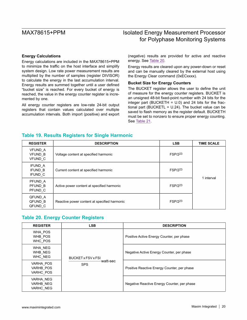
Table 19. Results Registers for Single Harmonic
Table 20. Energy Counter Registers
REGISTER DESCRIPTION LSB TIME SCALE
VFUND_AVFUND_BVFUND_C
Voltage content at specified harmonic FSP/223
1 interval
IFUND_AIFUND_BIFUND_C
Current content at specified harmonic FSP/223
PFUND_APFUND_BPFUND_C
Active power content at specified harmonic FSP/223
QFUND_AQFUND_BQFUND_C
Reactive power content at specified harmonic FSP/223
REGISTER LSB DESCRIPTION
WHA_POSWHB_POSWHC_POS
BUCKET x FSV x FSI
SPSwatt-sec
Positive Active Energy Counter, per phase
WHA_NEGWHB_NEGWHC_NEG
Negative Active Energy Counter, per phase
VARHA_POSVARHB_POSVARHC_POS
Positive Reactive Energy Counter, per phase
VARHA_NEGVARHB_NEGVARHC_NEG
Negative Reactive Energy Counter, per phase
MAX78615+PPM Isolated Energy Measurement Processor for Polyphase Monitoring Systems
www.maximintegrated.com Maxim Integrated 20
Example: 1Watt-hr bucket with a MAX78700 In this example, the full scale is assumed to be set as follows:FSV = 667V; FSI = 62A
( )Watthours Wh per count x 3600 sec / hr x SPS
BUCKET FSV x FSI
=
In order to set the energy bucket to 1Wh:
1 x 3600 x 3174.6BUCKET 276.3592
667 x 62= =
Therefore, the bucket register(s) value should be set as follows: BUCKET = BUCKETH + BUCKETL/224
BUCKETH = INT(BUCKET)BUCKETL = (BUCKET - INT(BUCKET)) x 224
BUCKETH = 276 = 0x000114BUCKETL = 0.3592 = 0x5BF722
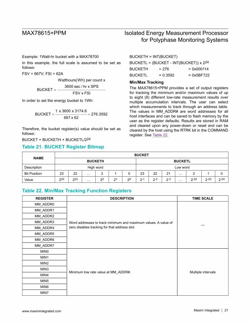
Min/Max TrackingThe MAX78615+PPM provides a set of output registers for tracking the minimum and/or maximum values of up to eight (8) different low-rate measurement results over multiple accumulation intervals. The user can select which measurements to track through an address table. The values in MM_ADDR# are word addresses for all host interfaces and can be saved to flash memory by the user as the register defaults. Results are stored in RAM and cleared upon any power-down or reset and can be cleared by the host using the RTRK bit in the COMMAND register. See Table 22.
Table 21. BUCKET Register Bitmap
Table 22. Min/Max Tracking Function Registers
NAMEBUCKET
BUCKETH BUCKETL
Description High word Low word
Bit Position 23 22 … 2 1 0 23 22 21 … 2 1 0
Value 223 222 … 22 21 20 2-1 2-2 2-3 … 2-22 2-23 2-24
REGISTER DESCRIPTION TIME SCALEMM_ADDR0
Word addresses to track minimum and maximum values. A value of zero disables tracking for that address slot. —
MM_ADDR1
MM_ADDR2
MM_ADDR3
MM_ADDR4
MM_ADDR5
MM_ADDR6
MM_ADDR7
MIN0
Minimum low rate value at MM_ADDR#. Multiple intervals
MIN1
MIN2
MIN3
MIN4
MIN5
MIN6
MIN7
MAX78615+PPM Isolated Energy Measurement Processor for Polyphase Monitoring Systems
www.maximintegrated.com Maxim Integrated 21

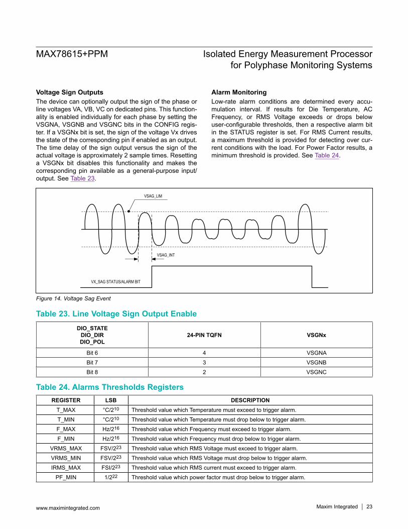
Voltage Sag DetectionThe MAX78615+PPM implements a voltage sag detec-tion function for each of the three phases. When a phase voltage drops below a programmable threshold, a cor-responding alarm is generated. The firmware computes the following indicator to detect whether the voltage falls below the threshold.
VSAG_INT 12 2
SAGX Xnn 0
V (v VSAG_LIM )−
=
= −∑
where: VSAG_LIM is the user-settable RMS value of the
voltage threshold. VSAG_INT is the user-settable number of high-rate
samples over which the indicators should be com-puted. For optimal performance, this should be set so that the resulting interval is an integer multiple of the line period (at least one half line period)
X is the phase (A, B, C).If VSAGX becomes negative, the firmware sets the VX_SAG bit for the corresponding phase in the STATUS register. If VX_SAG is enabled in a MASK register, the
corresponding pin is also be asserted low. If the VX_SAG bit is set in the STICKY register, then the alarm bit will remain set and any unmasked AL pin will remain low until the VX_SAG alarm is cleared via the STATUS_CLEAR register or the MAX78615+PPM is reset. If the VX_SAG bit is cleared in the STICKY register, then the alarm bit will be automatically cleared and any unmasked AL pin set high as soon as the indicator VSAGX is greater than the programmable threshold.The sag detection can be used to monitor or record the quality of the power line or utilize the sag alarm pin to notify external devices (for example a host microproces-sor) of a pending power-down. The external device can then enter a power-down mode (for example saving data or recording the event) before a power outage. Figure 14 shows a sag event and how the alarm bit is set by the firmware (in the case of the STICKY register bit cleared).Example: Set the detection interval to one-half of a line cycle (60Hz line frequency) with a MAX78700.
linesample
linesample
Tf 3174.62VSAG_INT 26.455
1 2f 2 x 60f
= = = =
Table 22. Min/Max Tracking Function Registers (continued)REGISTER DESCRIPTION TIME SCALE
MAX0
Maximum low rate value at MM_ADDR#. Multiple intervals
MAX1
MAX2
MAX3
MAX4
MAX5
MAX6
MAX7
Figure 13. Min/Max Tracking
MM_ADDR# RAM[#]
MAXIMUMMAX MAX#
MINIMUMMIN MIN#
CONTROL
MAX78615+PPM Isolated Energy Measurement Processor for Polyphase Monitoring Systems
www.maximintegrated.com Maxim Integrated 22
Voltage Sign OutputsThe device can optionally output the sign of the phase or line voltages VA, VB, VC on dedicated pins. This function-ality is enabled individually for each phase by setting the VSGNA, VSGNB and VSGNC bits in the CONFIG regis-ter. If a VSGNx bit is set, the sign of the voltage Vx drives the state of the corresponding pin if enabled as an output. The time delay of the sign output versus the sign of the actual voltage is approximately 2 sample times. Resetting a VSGNx bit disables this functionality and makes the corresponding pin available as a general-purpose input/output. See Table 23.
Alarm MonitoringLow-rate alarm conditions are determined every accu-mulation interval. If results for Die Temperature, AC Frequency, or RMS Voltage exceeds or drops below user-configurable thresholds, then a respective alarm bit in the STATUS register is set. For RMS Current results, a maximum threshold is provided for detecting over cur-rent conditions with the load. For Power Factor results, a minimum threshold is provided. See Table 24.
Table 23. Line Voltage Sign Output Enable
Table 24. Alarms Thresholds Registers
DIO_STATEDIO_DIRDIO_POL
24-PIN TQFN VSGNx
Bit 6 4 VSGNA
Bit 7 3 VSGNB
Bit 8 2 VSGNC
REGISTER LSB DESCRIPTIONT_MAX °C/210 Threshold value which Temperature must exceed to trigger alarm.
T_MIN °C/210 Threshold value which Temperature must drop below to trigger alarm.
F_MAX Hz/216 Threshold value which Frequency must exceed to trigger alarm.
F_MIN Hz/216 Threshold value which Frequency must drop below to trigger alarm.
VRMS_MAX FSV/223 Threshold value which RMS Voltage must exceed to trigger alarm.
VRMS_MIN FSV/223 Threshold value which RMS Voltage must drop below to trigger alarm.
IRMS_MAX FSI/223 Threshold value which RMS current must exceed to trigger alarm.
PF_MIN 1/222 Threshold value which power factor must drop below to trigger alarm.
Figure 14. Voltage Sag Event
VSAG_LIM
VSAG_INT
VX_SAG STATUS/ALARM BIT
MAX78615+PPM Isolated Energy Measurement Processor for Polyphase Monitoring Systems
www.maximintegrated.com Maxim Integrated 23
Imbalance of the three voltages and three currents is monitored and reported via dedicated alarm bits if they exceed respective maximum threshold V_IMB_MAX and I_IMB_MAX. See the Current and Voltage Imbalance sec-tion for details. See Table 25.The STATUS register also provides Sag voltage alarms. A configurable RMS voltage threshold and selectable Interval is provided as described below and in the Voltage Sag Detection section. See Table 26.
Status RegistersThe STATUS register is used to monitor the status of the device and user-configurable alarms. All other registers mentioned in this section share the same bit descriptions. The STICKY register determines which alarm/status bits are sticky and which track the current status of the con-dition. Each alarm bit defined as sticky (once triggered) holds its alarm status until the user clears it using the STATUS_RESET register. Any sticky bit not set allows the respective status bit to clear when the condition clears.The STATUS_SET and the STATUS_RESET registers allow the user to force status bits on or off, respectively, without fear of affecting unintended bits. A bit set in the STATUS_SET register sets the respective bit in the STATUS register, and a bit set in the STATUS_RESET register clears it. STATUS_SET and STATUS_RESET are both cleared after the status bit is set or reset. Table 27 lists the bit mapping for the all status-related registers.
Reset StateDuring and immediately after reset, all DIOs are config-ured as inputs until configured. Interface configuration
pins (IFC0/MP8, IFC1/MP0) and address pins (AD1/MP6, SCK/AD0/MP1) are input pins sampled during reset/ini-tialization to select the serial host interface and set device addresses (for I2C and UART modes). If the IFC0 pin is low, the device operates in the SPI mode. Otherwise, the state of IFC1 and the AD[1:0] pins determine the operat-ing mode and device address.
DIO_STATEThe DIO_STATE register contains the current status of the DIOs. The user can acquire the state of a DIO, if con-figured as input (1 = high, 0 = low), or control its state, if configured as output.
DIO_DIRThe DIO_DIR register sets the direction of the pins, where 1 is input and 0 is output. For pins used as part of the selected serial interface, the DIO_DIR register has no effect. If a DIO is defined as an input, a weak internal pullup is active. DIO pins must remain configured as an input if directly connecting to GND/VDD. Otherwise, it is recommended to use external pullup or pulldown resistors accordingly.
DIO_POLDIOs configured as outputs are by default active low. The logic 0 state is on. This can be modified using the DIO_POL register using the same bit definition as the DIO_STATE register. Any corresponding bit set in the DIO_POL register inverts the same DIO output so that it becomes active high.
Table 25. Imbalance Thresholds Registers
Table 26. Voltage Sag Thresholds Registers
REGISTER DESCRIPTION
V_IMB_MAX Percentage Threshold value which Voltage Imbalance must exceed to trigger alarm.
I_IMB_MAX Percentage Threshold value which Current Imbalance must exceed to trigger alarm.
REGISTER DESCRIPTION
VSAG_LIM Threshold value (in RMS) which voltage must go below to trigger a sag alarm.
VSAG_INT Interval (in samples) over which the voltage must be below the threshold. Should be set in increments of half cycles (i.e., 22 samples per half cycle at 60Hz).
MAX78615+PPM Isolated Energy Measurement Processor for Polyphase Monitoring Systems
www.maximintegrated.com Maxim Integrated 24
Table 27. Status-Related Registers Bitmap
Table 28. Digital I/O Functionality
BIT NAME STICKABLE? DESCRIPTION23 DRDY Yes New low rate results (data) ready
22 OV_FREQ Yes Frequency over High Limit
21 UN_FREQ Yes Under Low Frequency Limit
20 OV_TEMP Yes Temperature over High Limit
19 UN_TEMP Yes Under Low Temperature Limit
18 OV_VRMSC Yes RMS Voltage C Over Limit
17 UN_VRMSC Yes RMS Voltage C Under Limit
16 OV_VRMSB Yes RMS Voltage B Over Limit
15 UN_VRMSB Yes RMS Voltage B Under Limit
14 OV_VRMSA Yes RMS Voltage A Over Limit
13 UN_VRMSA Yes RMS Voltage A Under Limit
12 UN_PFC Yes Power Factor C Under Limit
11 UN_PFB Yes Power Factor B Under Limit
10 UN_PFA Yes Power Factor A Under Limit
9 OV_IRMSC Yes RMS Current C Over Limit
8 OV_IRMSB Yes RMS Current B Over Limit
7 OV_IRMSA Yes RMS Current A Over Limit
6 VC_SAG Yes Voltage C Sag Condition Detected
5 VB_SAG Yes Voltage B Sag Condition Detected
4 VA_SAG Yes Voltage A Sag Condition Detected
3 V_IMBAL Yes Voltage Imbalance Detected
2 I_IMBAL Yes Current Imbalance Detected
1 XSTATE No External Oscillator is clocking source
0 RESET Always Set by device after any type of reset
DIO_STATEDIO_DIRDIO_POL
24-PIN TQFN FUNCTION AT POWER-ON/RESET SPI UART I2C MASK
Bit 0 16 IFC1 MP0 —
Bit 1 15 AD0 SCK MP1 —
Bit 2 14 — SDI RX SDAI —
Bit 3 13 — SDO TX SDAO —
Bit 4 4 — MP4 MASK4
Bit 5 5 — SSB MP5 SCL —
Bit 6 4 AD1 MP6 —
Bit 7 3 — MP7 MASK7
Bit 8 2 IFC0 MP8 —
Bit 9:23 — — — —
MAX78615+PPM Isolated Energy Measurement Processor for Polyphase Monitoring Systems
www.maximintegrated.com Maxim Integrated 25
Alarm MasksThe device provides MASK registers for signaling the status of any STATUS bits to one of the MP pins. These MASK registers have the same bit mapping as the STATUS register. The user must first enable the respec-tive pin as an output before the MP can be driven to its active state. See Table 29.
Command RegisterThe Command Register is located at address 0x00. Use this register to perform specific tasks such as saving coefficients and nonvolatile register defaults into flash memory. It also allows initiation of integrated calibration routines. See Table 30.
Normal Operation The Normal Operations Command bits are applied in all normal operating cases. See Table 31.
Calibration Command The Calibration Command starts the calibration process for the selected inputs. It is assumed that appropriate input signals and target values are applied. When a gain calibration process completes, bits 23:17 are cleared along with bits associated with channels that calibrated successfully. When an offset calibration completes, 23:17 are cleared but the corresponding offset bits will remain set. See Table 32.
Table 29. Mask Registers
Table 32. Calibration Command Details
Table 30. Command Register Commands Table 31. Normal Operation Command Details
Note: During calibration, the “line-lock” bit should be set for best results.
PIN NAME REGISTER DESCRIPTION
MP4 MASK4 A combination of a bit set in both the STATUS register and a MASK register causes the assigned DIO_STATE/pin to be activated (default active-low).MP7 MASK7
VALUE (HEX) DESCRIPTION0x00xxxx Normal Operations Command
0xCA/CBxxxx Calibration Command
0xACCxxx Flash Access Command
0xBDxxxx Soft Reset Command
0xECxxxx Reset Energy Command
BIT(S) VALUE DESCRIPTION
6 RTRK
1= reset the minima and maxima registers for all monitored variables. This bit automatically clears to zero when the reset completes.
BIT(S) VALUE DESCRIPTION
23:17 0x65 “Calibrate” Command
16 1 = Calibrate Voltage for Phase C, 0 = no action
15 1 = Calibrate Voltage for Phase B, 0 = no action
14 1 = Calibrate Voltage for Phase A, 0 = no action
13 1 = Calibrate Current for Phase C, 0 = no action
12 1 = Calibrate Current for Phase B, 0 = no action
11 1 = Calibrate Current for Phase A, 0 = no action
10 1 = Calibrate Temperature, 0 = no action
9 Calibrate Offset vs. Gain (0 = calibrate Gain; 1 = calibrate Offset)
8:0 Reserved, set to 0
MAX78615+PPM Isolated Energy Measurement Processor for Polyphase Monitoring Systems
www.maximintegrated.com Maxim Integrated 26
Examples:
Calibrate gains of voltage and current of Phase A
Start Command: COMMAND = 0xCA4830
Successful Calibration: COMMAND is reset to 0x000030
Calibration of current failed: COMMAND is reset to 0x000830
Calibrate gains of all three voltages.
Start Command: COMMAND = 0xCBC030
Successful Calibration: COMMAND is reset to 0x000030
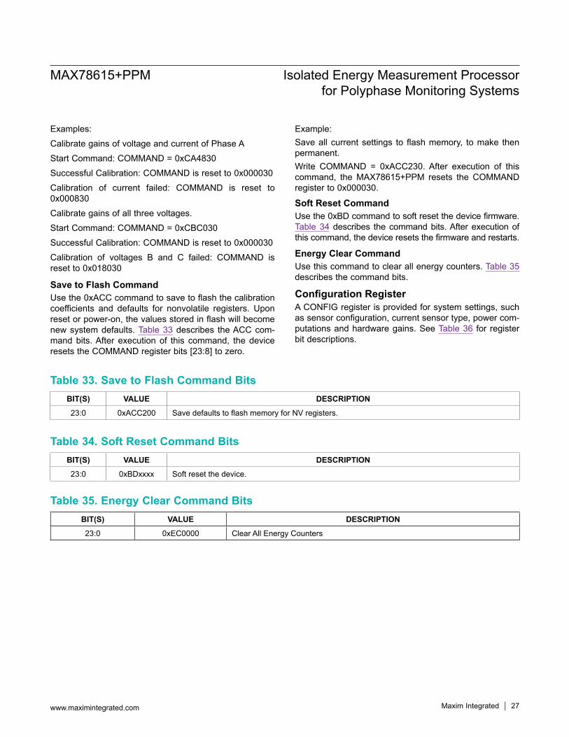
Calibration of voltages B and C failed: COMMAND is reset to 0x018030
Save to Flash Command Use the 0xACC command to save to flash the calibration coefficients and defaults for nonvolatile registers. Upon reset or power-on, the values stored in flash will become new system defaults. Table 33 describes the ACC com-mand bits. After execution of this command, the device resets the COMMAND register bits [23:8] to zero.
Example: Save all current settings to flash memory, to make then permanent. Write COMMAND = 0xACC230. After execution of this command, the MAX78615+PPM resets the COMMAND register to 0x000030.
Soft Reset Command Use the 0xBD command to soft reset the device firmware. Table 34 describes the command bits. After execution of this command, the device resets the firmware and restarts.
Energy Clear Command Use this command to clear all energy counters. Table 35 describes the command bits.
Configuration RegisterA CONFIG register is provided for system settings, such as sensor configuration, current sensor type, power com-putations and hardware gains. See Table 36 for register bit descriptions.
Table 33. Save to Flash Command Bits
Table 34. Soft Reset Command Bits
Table 35. Energy Clear Command Bits
BIT(S) VALUE DESCRIPTION
23:0 0xACC200 Save defaults to flash memory for NV registers.
BIT(S) VALUE DESCRIPTION
23:0 0xBDxxxx Soft reset the device.
BIT(S) VALUE DESCRIPTION
23:0 0xEC0000 Clear All Energy Counters
MAX78615+PPM Isolated Energy Measurement Processor for Polyphase Monitoring Systems
www.maximintegrated.com Maxim Integrated 27

Table 36. CONFIG Register Bit DescriptionsBIT(S) NAME DESCRIPTION
23 — Reserved for future use, write as zeroes
22 INV_AV3 Invert voltage samples AV3
21 INV_AV2 Invert voltage samples AV2
20 INV_AV1 Invert voltage samples AV1
19 VSGNC Drive MP8 with sign of voltage C
18 VSGNB Drive MP7 with sign of voltage B
17 VSGNA Drive MP6 with sign of voltage A
16 — Reserved for future use, write as zeroes
15 — Reserved for future use, write as zeroes
14 — Reserved for future use, write as zeroes
13 — Reserved for future use, write as zeroes
12 — Reserved for future use, write as zeroes
11 — Reserved for future use, write as zeroes
10 — Reserved for future use, write as zeroes
9 — Reserved for future use, write as zeroes
8 — Reserved for future use, write as zeroes
7:6 PPHASE
Ignore phase for total power computations00: none01: phase A10: phase B11: phase C
5 VDELTA Compute delta voltage between phases
4:3 VPHASE
Missing sensor on voltage input00: none missing01: AV110: AV211: AV3
2 INEUTRAL Current sensor in neutral leg.
1:0 IPHASE
Missing sensor on current input00: none missing01: AI110: AI211: AI3
MAX78615+PPM Isolated Energy Measurement Processor for Polyphase Monitoring Systems
www.maximintegrated.com Maxim Integrated 28
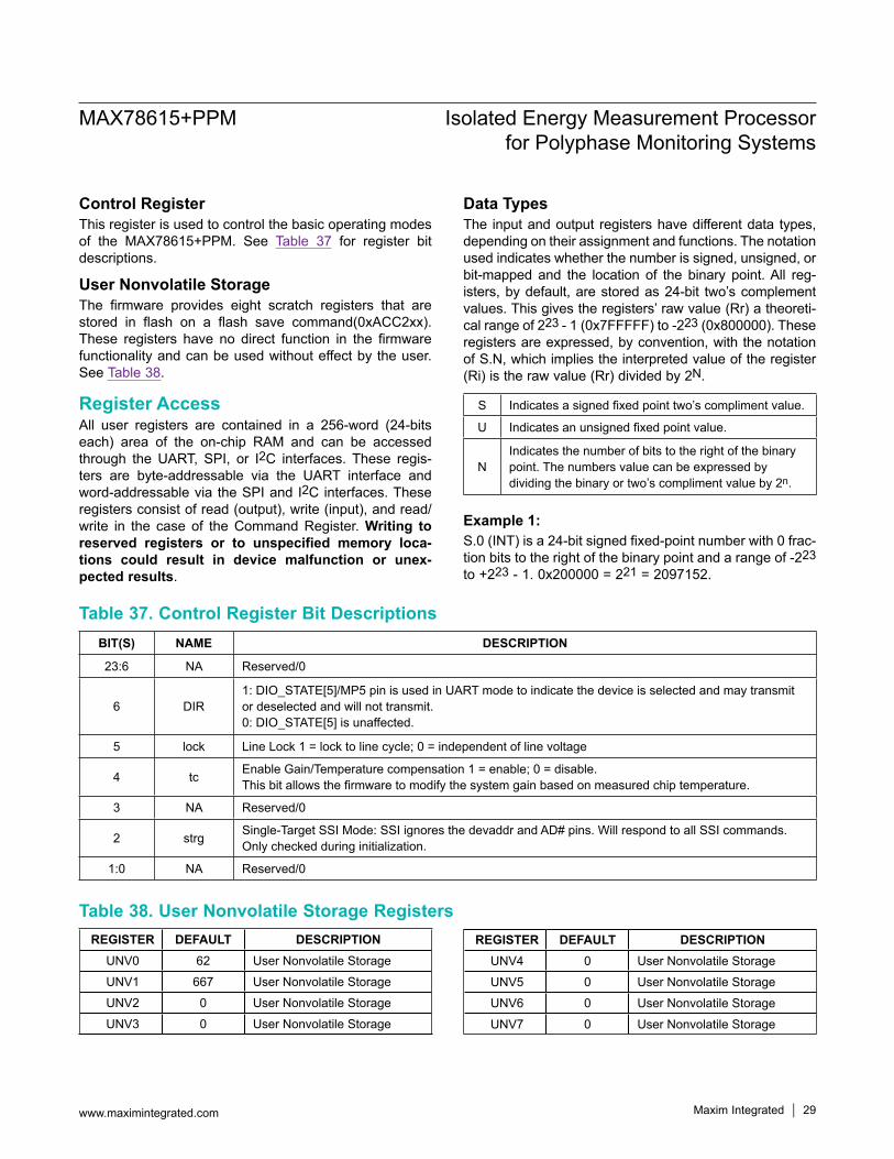
Control RegisterThis register is used to control the basic operating modes of the MAX78615+PPM. See Table 37 for register bit descriptions.
User Nonvolatile StorageThe firmware provides eight scratch registers that are stored in flash on a flash save command(0xACC2xx). These registers have no direct function in the firmware functionality and can be used without effect by the user. See Table 38.
Register Access All user registers are contained in a 256-word (24-bits each) area of the on-chip RAM and can be accessed through the UART, SPI, or I2C interfaces. These regis-ters are byte-addressable via the UART interface and word-addressable via the SPI and I2C interfaces. These registers consist of read (output), write (input), and read/write in the case of the Command Register. Writing to reserved registers or to unspecified memory loca-tions could result in device malfunction or unex-pected results.
Data TypesThe input and output registers have different data types, depending on their assignment and functions. The notation used indicates whether the number is signed, unsigned, or bit-mapped and the location of the binary point. All reg-isters, by default, are stored as 24-bit two’s complement values. This gives the registers’ raw value (Rr) a theoreti-cal range of 223 - 1 (0x7FFFFF) to -223 (0x800000). These registers are expressed, by convention, with the notation of S.N, which implies the interpreted value of the register (Ri) is the raw value (Rr) divided by 2N.
Example 1:S.0 (INT) is a 24-bit signed fixed-point number with 0 frac-tion bits to the right of the binary point and a range of -223 to +223 - 1. 0x200000 = 221 = 2097152.
Table 37. Control Register Bit Descriptions
Table 38. User Nonvolatile Storage Registers
S Indicates a signed fixed point two’s compliment value.
U Indicates an unsigned fixed point value.
NIndicates the number of bits to the right of the binary point. The numbers value can be expressed by dividing the binary or two’s compliment value by 2n.
REGISTER DEFAULT DESCRIPTIONUNV0 62 User Nonvolatile Storage
UNV1 667 User Nonvolatile Storage
UNV2 0 User Nonvolatile Storage
UNV3 0 User Nonvolatile Storage
REGISTER DEFAULT DESCRIPTIONUNV4 0 User Nonvolatile Storage
UNV5 0 User Nonvolatile Storage
UNV6 0 User Nonvolatile Storage
UNV7 0 User Nonvolatile Storage
BIT(S) NAME DESCRIPTION
23:6 NA Reserved/0
6 DIR1: DIO_STATE[5]/MP5 pin is used in UART mode to indicate the device is selected and may transmit or deselected and will not transmit.0: DIO_STATE[5] is unaffected.
5 lock Line Lock 1 = lock to line cycle; 0 = independent of line voltage
4 tc Enable Gain/Temperature compensation 1 = enable; 0 = disable.This bit allows the firmware to modify the system gain based on measured chip temperature.
3 NA Reserved/0
2 strg Single-Target SSI Mode: SSI ignores the devaddr and AD# pins. Will respond to all SSI commands. Only checked during initialization.
1:0 NA Reserved/0
MAX78615+PPM Isolated Energy Measurement Processor for Polyphase Monitoring Systems
www.maximintegrated.com Maxim Integrated 29

Example 2:S.21 is a 24-bit signed fixed-point number with 21 fraction bits to the right of the binary point and a range of -4.0 to 4-2-21. The value can be expressed by dividing the two’s compliment value by 221. 0x200000 = 1. 0x800000 = -4.0.
Example 3:U.24 is a 24-bit unsigned fixed-point number with 24 fraction bits to the right of the binary point and a range of 1.0-2X to 0. The value can be expressed by dividing the binary value by 2X = 2X = 0.125. 0x800000 = 2X = 0.5.
Indirect Read AccessThe device firmware supplies a method for indirect read access to the device RAM memory. The firmware writes the contents of IND_RD_DATA with the content of RAM at the word address indicated by (IND_RD_ADDR and 0x0000FF). That value (IND_RD_ADDR and 0x0000FF) is then written back into IND_RD_ADDR to indicate the read has completed. The check/action for the contents of
IND_RD_ADDR is performed at every high rate sample. See Table 39.
Indirect Write AccessThe device firmware supplies a method for indirect write access to the device RAM memory. If any of the upper 12 bits of IND_WR_ADDR are nonzero, the firmware writes the contents of IND_WR_DATA into the word address indicated by (IND_WR_ADDR and 0x0000FF). That value (IND_WR_ADDR and 0x0000FF) is then written back into IND_WR_ADDR to indicate the write has completed. The check/action for the contents of IND_WR_ADDR is per-formed at every high rate sample. See Table 40.
Register LocationsUse word addresses for I2C and SPI interfaces and byte addresses for the SSI (UART) protocol. Nonvolatile (NV) register defaults are indicated with a “Y.” All other registers are initialized as described in the Functional Description. See Table 41.
Table 39. Indirect Read Access Registers
Table 41. Register Map
Table 40. Direct Read Access RegistersREGISTER DESCRIPTION
IND_RD_ADDR Indirect Read Address
IND_RD_DATA Indirect Read Data
REGISTER DESCRIPTION
IND_WR_DATA Indirect Write Data
IND_WR_ADDR Indirect Write Address
WORD ADDR(HEX)
BYTE ADDR(HEX)
REGISTER NAME TYPE NV DESCRIPTION
0 0 COMMAND INT Y Firmware action/commands
1 3 FW_VERSION INT Firmware version
2 6 CONFIG INT Y Selects input configuration
3 9 CONTROL INT Y Device behavior control
4 C CYCLE INT High-rate sample counter
5 F DIVISOR INT Actual samples in previous accumulation interval
6 12 FRAME INT Low-rate sample counter
7 15 STATUS INT Alarm and device status bits
8 18 DIO_STATE INT State of DIO pins
9 1B IND_WR_DATA INT Indirect Write Data
A 1E IND_WR_ADDR INT Indirect Write Address
B 21 IND_RD_ADDR INT Indirect Read Address
MAX78615+PPM Isolated Energy Measurement Processor for Polyphase Monitoring Systems
www.maximintegrated.com Maxim Integrated 30
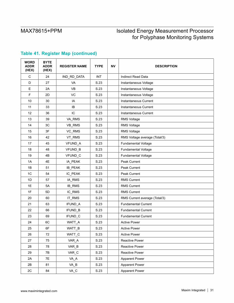
Table 41. Register Map (continued)
WORD ADDR(HEX)
BYTE ADDR(HEX)
REGISTER NAME TYPE NV DESCRIPTION
C 24 IND_RD_DATA INT Indirect Read Data
D 27 VA S.23 Instantaneous Voltage
E 2A VB S.23 Instantaneous Voltage
F 2D VC S.23 Instantaneous Voltage
10 30 IA S.23 Instantaneous Current
11 33 IB S.23 Instantaneous Current
12 36 IC S.23 Instantaneous Current
13 39 VA_RMS S.23 RMS Voltage
14 3C VB_RMS S.23 RMS Voltage
15 3F VC_RMS S.23 RMS Voltage
16 42 VT_RMS S.23 RMS Voltage average (Total/3)
17 45 VFUND_A S.23 Fundamental Voltage
18 48 VFUND_B S.23 Fundamental Voltage
19 4B VFUND_C S.23 Fundamental Voltage
1A 4E IA_PEAK S.23 Peak Current
1B 51 IB_PEAK S.23 Peak Current
1C 54 IC_PEAK S.23 Peak Current
1D 57 IA_RMS S.23 RMS Current
1E 5A IB_RMS S.23 RMS Current
1F 5D IC_RMS S.23 RMS Current
20 60 IT_RMS S.23 RMS Current average (Total/3)
21 63 IFUND_A S.23 Fundamental Current
22 66 IFUND_B S.23 Fundamental Current
23 69 IFUND_C S.23 Fundamental Current
24 6C WATT_A S.23 Active Power
25 6F WATT_B S.23 Active Power
26 72 WATT_C S.23 Active Power
27 75 VAR_A S.23 Reactive Power
28 78 VAR_B S.23 Reactive Power
29 7B VAR_C S.23 Reactive Power
2A 7E VA_A S.23 Apparent Power
2B 81 VA_B S.23 Apparent Power
2C 84 VA_C S.23 Apparent Power
MAX78615+PPM Isolated Energy Measurement Processor for Polyphase Monitoring Systems
www.maximintegrated.com Maxim Integrated 31
Table 41. Register Map (continued)
WORD ADDR(HEX)
BYTE ADDR(HEX)
REGISTER NAME TYPE NV DESCRIPTION
2D 87 WATT_T S.23 Active Power Total
2E 8A VAR_T S.23 Reactive Power Total
2F 8D VA_T S.23 Apparent Power Total
30 90 PFUND_A S.23 Fundamental Power
31 93 PFUND_B S.23 Fundamental Power
32 96 PFUND_C S.23 Fundamental Power
33 99 QFUND_A S.23 Fundamental Reactive Power
34 9C QFUND_B S.23 Fundamental Reactive Power
35 9F QFUND_C S.23 Fundamental Reactive Power
36 A2 VAFUNDA S.23 Fundamental Volt Amperes
37 A5 VAFUNDB S.23 Fundamental Volt Amperes
38 A8 VAFUNDC S.23 Fundamental Volt Amperes
39 AB PFA S.22 Power Factor
3A AE PFB S.22 Power Factor
3B B1 PFC S.22 Power Factor
3C B4 PF_T S.22 Total Power Factor
3D B7 FREQ S.16 Line Frequency
3E BA TEMPC_A S.10 Chip Temperature (Celsius°) Channel A
3F BD TEMPC_B S.10 Chip Temperature (Celsius°) Channel B
40 C0 TEMPC_C S.10 Chip Temperature (Celsius°) Channel C
41 C3 WHA_POS INT Received Active Energy Counter
42 C6 WHB_POS INT Received Active Energy Counter
43 C9 WHC_POS INT Received Active Energy Counter
44 CC WHA_NEG INT Delivered Active Energy Counter
45 CF WHB_NEG INT Delivered Active Energy Counter
46 D2 WHC_NEG INT Delivered Active Energy Counter
47 D5 VARHA_POS INT Reactive Energy Leading Counter
48 D8 VARHB_POS INT Reactive Energy Leading Counter
49 DB VARHC_POS INT Reactive Energy Leading Counter
4A DE VARHA_NEG INT Reactive Energy Lagging Counter
4B E1 VARHB_NEG INT Reactive Energy Lagging Counter
4C E4 VARHC_NEG INT Reactive Energy Lagging Counter
4D E7 MIN0 NA Minimum Recorded Value 1
MAX78615+PPM Isolated Energy Measurement Processor for Polyphase Monitoring Systems
www.maximintegrated.com Maxim Integrated 32
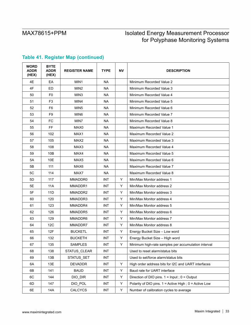
Table 41. Register Map (continued)
WORD ADDR(HEX)
BYTE ADDR(HEX)
REGISTER NAME TYPE NV DESCRIPTION
4E EA MIN1 NA Minimum Recorded Value 2
4F ED MIN2 NA Minimum Recorded Value 3
50 F0 MIN3 NA Minimum Recorded Value 4
51 F3 MIN4 NA Minimum Recorded Value 5
52 F6 MIN5 NA Minimum Recorded Value 6
53 F9 MIN6 NA Minimum Recorded Value 7
54 FC MIN7 NA Minimum Recorded Value 8
55 FF MAX0 NA Maximum Recorded Value 1
56 102 MAX1 NA Maximum Recorded Value 2
57 105 MAX2 NA Maximum Recorded Value 3
58 108 MAX3 NA Maximum Recorded Value 4
59 10B MAX4 NA Maximum Recorded Value 5
5A 10E MAX5 NA Maximum Recorded Value 6
5B 111 MAX6 NA Maximum Recorded Value 7
5C 114 MAX7 NA Maximum Recorded Value 8
5D 117 MMADDR0 INT Y Min/Max Monitor address 1
5E 11A MMADDR1 INT Y Min/Max Monitor address 2
5F 11D MMADDR2 INT Y Min/Max Monitor address 3
60 120 MMADDR3 INT Y Min/Max Monitor address 4
61 123 MMADDR4 INT Y Min/Max Monitor address 5
62 126 MMADDR5 INT Y Min/Max Monitor address 6
63 129 MMADDR6 INT Y Min/Max Monitor address 7
64 12C MMADDR7 INT Y Min/Max Monitor address 8
65 12F BUCKETL INT Y Energy Bucket Size – Low word
66 132 BUCKETH INT Y Energy Bucket Size – High word
67 135 SAMPLES INT Y Minimum high-rate samples per accumulation interval
68 138 STATUS_CLEAR INT Used to reset alarm/status bits
69 13B STATUS_SET INT Used to set/force alarm/status bits
6A 13E DEVADDR INT Y High order address bits for I2C and UART interfaces
6B 141 BAUD INT Y Baud rate for UART interface
6C 144 DIO_DIR INT Y Direction of DIO pins. 1 = Input ; 0 = Output
6D 147 DIO_POL INT Y Polarity of DIO pins. 1 = Active High ; 0 = Active Low
6E 14A CALCYCS INT Y Number of calibration cycles to average
MAX78615+PPM Isolated Energy Measurement Processor for Polyphase Monitoring Systems
www.maximintegrated.com Maxim Integrated 33

Table 41. Register Map (continued)WORD ADDR(HEX)
BYTE ADDR(HEX)
REGISTER NAME TYPE NV DESCRIPTION
6F 14D HPF_COEF_I S.23 Y Current input HPF coefficient. Positive values only
70 150 HPF_COEF_V S.23 Y Voltage input HPF coefficient. Positive values only
71 153 PHASECOMP1 S.21 Y Phase compensation (±4 samples) for AV1 input
72 156 PHASECOMP2 S.21 Y Phase compensation (±4 samples) for AV2 input
73 159 PHASECOMP3 S.22 Y Phase compensation (±4 samples) for AV3 input
74 15C HARM INT Y Harmonic Selector, default: 1 (fundamental)
75 15E V1_OFFS S.23 Y Voltage Offset Calibration
76 162 V2_OFFS S.23 Y Voltage Offset Calibration
77 165 V3_OFFS S.23 Y Voltage Offset Calibration
78 168 V1_GAIN S.21 Y Voltage Gain Calibration. Positive values only
79 16B V2_GAIN S.21 Y Voltage Gain Calibration. Positive values only
7A 16E V3_GAIN S.21 Y Voltage Gain Calibration. Positive values only
7B 171 I1_OFFS S.23 Y Current Offset Calibration
7C 174 I2_OFFS S.23 Y Current Offset Calibration
7D 177 I3_OFFS S.23 Y Current Offset Calibration
7E 17A I1_GAIN S.21 Y Current Gain Calibration. Positive values only.
7F 17D I2_GAIN S.21 Y Current Gain Calibration. Positive values only.
80 180 I3_GAIN S.21 Y Current Gain Calibration. Positive values only.
81 183 IARMS_OFF S.23 Y RMS Current dynamic offset adjust. Positive values only.
82 186 IBRMS_OFF S.23 Y RMS Current dynamic offset adjust. Positive values only.
83 189 ICRMS_OFF S.23 Y RMS Current dynamic offset adjust. Positive values only.
84 18C QA_OFFS S.23 Y Reactive Power dynamic offset adjust. Positive values only.
85 18F QB_OFFS S.23 Y Reactive Power dynamic offset adjust. Positive values only.
86 192 QC_OFFS S.23 Y Reactive Power dynamic offset adjust. Positive values only.
87 195 PA_OFFS S.23 Y Active Power dynamic offset adjust. Positive values only.
88 198 PB_OFFS S.23 Y Active Power dynamic offset adjust. Positive values only.
89 19B PC_OFFS S.23 Y Active Power dynamic offset adjust. Positive values only.
8A 19E T_GAIN S.21 Y Temperature Slope Calibration (Factory Set)
8B 1A1 T_OFFS1 INT Y Temperature Offset Calibration Remote Channel 1
8C 1A4 T_OFFS2 INT Y Temperature Offset Calibration Remote Ch. B
8D 1A7 T_OFFS3 INT Y Temperature Offset Calibration Remote Ch. C
8E 1AA VSAG_INT INT Y Voltage sag detect interval (high-rate samples)
8F 1AD V_IMB_MAX S.23 Y Voltage imbalance alarm limit. Positive values only
MAX78615+PPM Isolated Energy Measurement Processor for Polyphase Monitoring Systems
www.maximintegrated.com Maxim Integrated 34
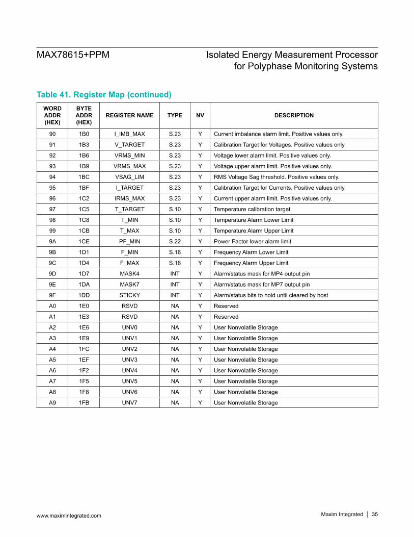
Table 41. Register Map (continued)WORD ADDR(HEX)
BYTE ADDR(HEX)
REGISTER NAME TYPE NV DESCRIPTION
90 1B0 I_IMB_MAX S.23 Y Current imbalance alarm limit. Positive values only.
91 1B3 V_TARGET S.23 Y Calibration Target for Voltages. Positive values only.
92 1B6 VRMS_MIN S.23 Y Voltage lower alarm limit. Positive values only.
93 1B9 VRMS_MAX S.23 Y Voltage upper alarm limit. Positive values only.
94 1BC VSAG_LIM S.23 Y RMS Voltage Sag threshold. Positive values only.
95 1BF I_TARGET S.23 Y Calibration Target for Currents. Positive values only.
96 1C2 IRMS_MAX S.23 Y Current upper alarm limit. Positive values only.
97 1C5 T_TARGET S.10 Y Temperature calibration target
98 1C8 T_MIN S.10 Y Temperature Alarm Lower Limit
99 1CB T_MAX S.10 Y Temperature Alarm Upper Limit
9A 1CE PF_MIN S.22 Y Power Factor lower alarm limit
9B 1D1 F_MIN S.16 Y Frequency Alarm Lower Limit
9C 1D4 F_MAX S.16 Y Frequency Alarm Upper Limit
9D 1D7 MASK4 INT Y Alarm/status mask for MP4 output pin
9E 1DA MASK7 INT Y Alarm/status mask for MP7 output pin
9F 1DD STICKY INT Y Alarm/status bits to hold until cleared by host
A0 1E0 RSVD NA Y Reserved
A1 1E3 RSVD NA Y Reserved
A2 1E6 UNV0 NA Y User Nonvolatile Storage
A3 1E9 UNV1 NA Y User Nonvolatile Storage
A4 1FC UNV2 NA Y User Nonvolatile Storage
A5 1EF UNV3 NA Y User Nonvolatile Storage
A6 1F2 UNV4 NA Y User Nonvolatile Storage
A7 1F5 UNV5 NA Y User Nonvolatile Storage
A8 1F8 UNV6 NA Y User Nonvolatile Storage
A9 1FB UNV7 NA Y User Nonvolatile Storage
MAX78615+PPM Isolated Energy Measurement Processor for Polyphase Monitoring Systems
www.maximintegrated.com Maxim Integrated 35

Serial InterfacesAll user registers are contained in a 256-word (24-bits each) area of the on-chip RAM and can be accessed through the UART, SPI, or I2C interfaces. While access to a single byte is possible with some interfaces, it is highly recommended that the user access words (or multiple words) of data with each transaction. Only one interface can be active at a time. The interface selection pins are sampled at the end of a reset or power-on sequence to determine the operating mode. See Table 42.
UART InterfaceThe device implements a “simple serial interface” (SSI) protocol on the UART interface that features:
Support for single and multipoint communications Transmit (direction) control for an RS-485 transceiver Efficient use of a low bandwidth serial interface Data integrity checking
The default configuration is 38400 baud, 8-bit, no-parity, 1 stop-bit, no flow control. The value in the BAUD register
determines the baud rate to be used. Example: To select a 9600 baud rate, the user writes a decimal 9600 to the BAUD register. The new rate will not take effect immedi-ately. It must be saved to flash and takes effect at the next reset. The maximum BAUD value is limited to 115200.
RS-485 SupportThe SSB/MP5/SCL pin can be used to drive an RS-485 transceiver output enable or direction pin. The implement-ed protocol supports a full-duplex 4-wire RS-485 bus. When the DIR bit is set in the Control Register, then the DIO_STATE[5] pin reflects if the device has been selected or deselected by an SSI target command. If DIO_DIR[5] is also set to an output, then the MP5 pin reflects this state. See Figure 15.
Table 42. Serial Interface SelectionINTERFACE MODE IFC0 IFC1
SPI 0 X (don’t care)
UART 1 0
I2C 1 1
Figure 15. RS-485 Bus Protocol
Figure 16. Multipoint Device Address Communication System
RS-485 BUS
AROUT
REN
DEN
DIN
SDI/RX/SDAI
SSB/MP5/SCL
SDO/TX/SDAO
4.7KΩ
RS-485 BUS
MAX78615+PPM
B
A
B
DEVADDR[7:2]
AD1
AD0
I2C DEVICE ADDRESS
+1 =
SSI ID
7 6 5 4 3 2 1 0 7 6 5 4 3 2 1 0
MAX78615+PPM Isolated Energy Measurement Processor for Polyphase Monitoring Systems
www.maximintegrated.com Maxim Integrated 36

Device Address ConfigurationThe SSI protocol utilizes 8-bit addressing for multipoint communications. The usable SSI ID range is 1 to 254. In multipoint systems with more than four targets, the user must configure device address bits in the DEVADDR according to the formula SSI ID = Device Address +1 (Figure 16).If the CONTROL[2]/strg bit is set on startup, then the SSI protocol assumes it is the only device in the system and ignore the SSI ID and responds to all commands. See Table 43.
SSI Protocol DescriptionThe SSI protocol is command response system supporting a single master and one or more targets. The host (master) sends commands to a selected target that first verifies the integrity of the packet before sending a reply or executing a command. Failure to decode a host packet will cause the selected target to send a fail code. If the condition of a received packet is uncertain, no reply is sent. Each target must have a unique SSI ID. Zero is not a valid SSI ID for a target device as it is used by the host to de-select all target devices. With both address pins low on the MAX78615+PPM, the SSI ID defaults to 1 and is the “Selected” device following a reset. This configuration is intended for single target (point-to-point) systems that do not require the use of device addressing or selecting targets.
In multipoint systems, the master typically de-selects all target devices by selecting SSI ID #0. The master must then select the target with a valid SSI ID and get an acknowledgement from the slave before setting the target’s register address pointer and performing read or write operations. If no target is selected, no reply is sent. The SSB/MP5/SCL pin is asserted while the device is selected. Figure 17 shows the sequence of operation.
Master PacketsMaster packets always start with the 1-byte header (0xAA) for synchronization purposes. The master then sends the byte count of the entire packet (up to 255 byte packets) followed by the payload (up to 253 bytes) and a 1-byte modulo-256 checksum of all packet bytes for data integrity checking. See Figure 18.The payload can contain either a single command or multiple commands if the target is already selected. It can also include device addresses, register addresses, and data. All multibyte payloads are sent and received least-significant-byte first. See Table 44 for the master packet command summary.Users only need to implement commands they actually need or intend to use. For example, only one address command is required, either 0xA1 for systems with 8 address bits or less or 0xA3 for systems with 9 to 16 address bits. Likewise, only one write, read, or select tar-get command needs to be implemented. Select Target is not needed in systems with only one target.
Table 43. Single Target Mode BitNAME DEFAULT DESCRIPTION
strg 1 1: Single-Target SSI Mode: SSI ignores devaddr and will respond to all SSI commands. Only checked during initialization.
Figure 17. SSI Protocol System Sequence
Figure 18. Master Packets
SELECT TARGET DEVICE
SET REGISTER ADDRESS POINTER
READ/WRITE COMMANDS
DE-SELECT TARGET DEVICE
HEADER(0xAA)
BYTECOUNT PAYLOAD CHECKSUM
MAX78615+PPM Isolated Energy Measurement Processor for Polyphase Monitoring Systems
www.maximintegrated.com Maxim Integrated 37
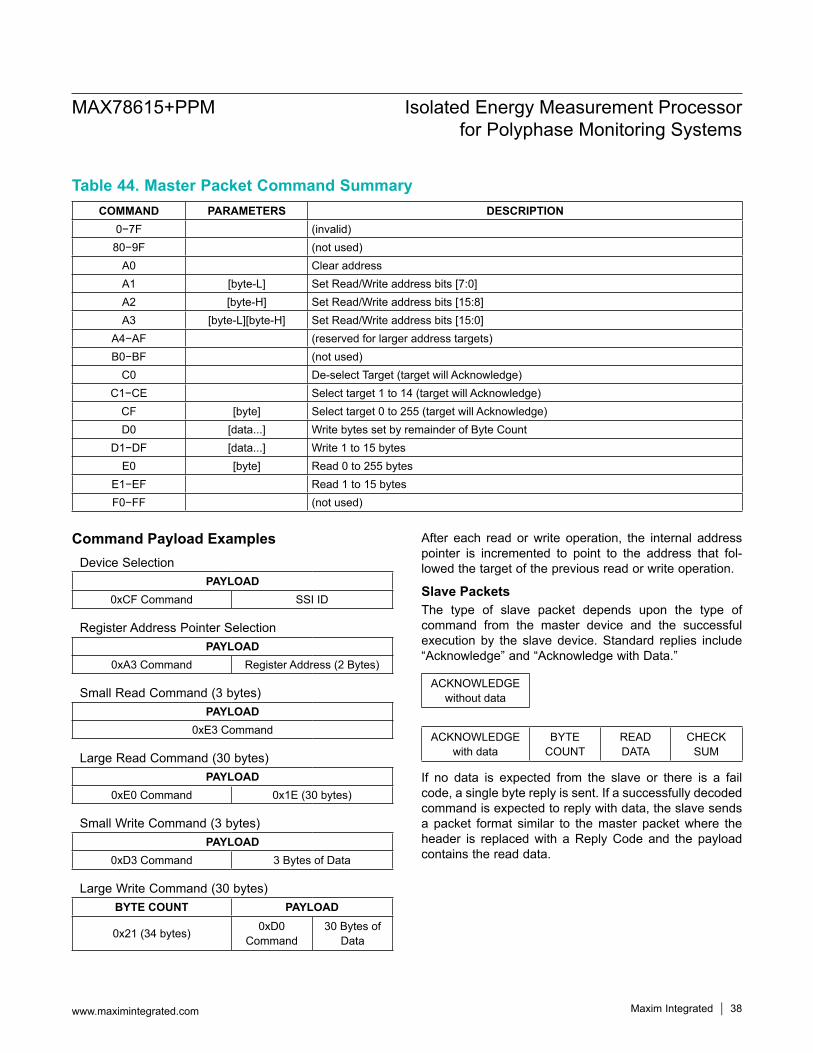
Command Payload Examples After each read or write operation, the internal address pointer is incremented to point to the address that fol-lowed the target of the previous read or write operation.
Slave PacketsThe type of slave packet depends upon the type of command from the master device and the successful execution by the slave device. Standard replies include “Acknowledge” and “Acknowledge with Data.”
If no data is expected from the slave or there is a fail code, a single byte reply is sent. If a successfully decoded command is expected to reply with data, the slave sends a packet format similar to the master packet where the header is replaced with a Reply Code and the payload contains the read data.
Table 44. Master Packet Command SummaryCOMMAND PARAMETERS DESCRIPTION
0−7F (invalid)80−9F (not used)
A0 Clear addressA1 [byte-L] Set Read/Write address bits [7:0]A2 [byte-H] Set Read/Write address bits [15:8]A3 [byte-L][byte-H] Set Read/Write address bits [15:0]
A4−AF (reserved for larger address targets)B0−BF (not used)
C0 De-select Target (target will Acknowledge)C1−CE Select target 1 to 14 (target will Acknowledge)
CF [byte] Select target 0 to 255 (target will Acknowledge)D0 [data...] Write bytes set by remainder of Byte Count
D1−DF [data...] Write 1 to 15 bytesE0 [byte] Read 0 to 255 bytes
E1−EF Read 1 to 15 bytesF0−FF (not used)
Device SelectionPAYLOAD
0xCF Command SSI ID
Register Address Pointer SelectionPAYLOAD
0xA3 Command Register Address (2 Bytes)
Small Read Command (3 bytes)PAYLOAD
0xE3 Command
Large Read Command (30 bytes)PAYLOAD
0xE0 Command 0x1E (30 bytes)
Small Write Command (3 bytes)PAYLOAD
0xD3 Command 3 Bytes of Data
Large Write Command (30 bytes)BYTE COUNT PAYLOAD
0x21 (34 bytes) 0xD0 Command
30 Bytes of Data
ACKNOWLEDGEwithout data
ACKNOWLEDGEwith data
BYTECOUNT
READDATA
CHECKSUM
MAX78615+PPM Isolated Energy Measurement Processor for Polyphase Monitoring Systems
www.maximintegrated.com Maxim Integrated 38
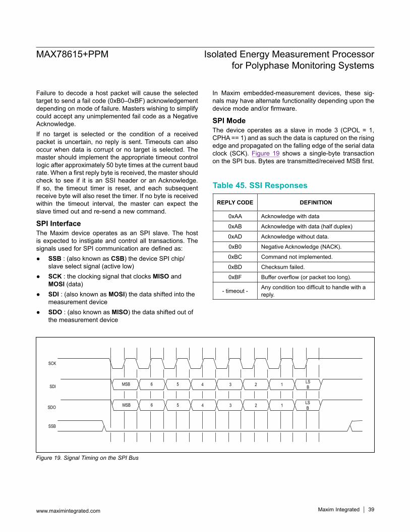
Failure to decode a host packet will cause the selected target to send a fail code (0xB0–0xBF) acknowledgement depending on mode of failure. Masters wishing to simplify could accept any unimplemented fail code as a Negative Acknowledge. If no target is selected or the condition of a received packet is uncertain, no reply is sent. Timeouts can also occur when data is corrupt or no target is selected. The master should implement the appropriate timeout control logic after approximately 50 byte times at the current baud rate. When a first reply byte is received, the master should check to see if it is an SSI header or an Acknowledge. If so, the timeout timer is reset, and each subsequent receive byte will also reset the timer. If no byte is received within the timeout interval, the master can expect the slave timed out and re-send a new command.
SPI InterfaceThe Maxim device operates as an SPI slave. The host is expected to instigate and control all transactions. The signals used for SPI communication are defined as:
SSB : (also known as CSB) the device SPI chip/slave select signal (active low)
SCK : the clocking signal that clocks MISO and MOSI (data)
SDI : (also known as MOSI) the data shifted into the measurement device
SDO : (also known as MISO) the data shifted out of the measurement device
In Maxim embedded-measurement devices, these sig-nals may have alternate functionality depending upon the device mode and/or firmware.
SPI ModeThe device operates as a slave in mode 3 (CPOL = 1, CPHA == 1) and as such the data is captured on the rising edge and propagated on the falling edge of the serial data clock (SCK). Figure 19 shows a single-byte transaction on the SPI bus. Bytes are transmitted/received MSB first.
Table 45. SSI Responses
REPLY CODE DEFINITION
0xAA Acknowledge with data
0xAB Acknowledge with data (half duplex)
0xAD Acknowledge without data.
0xB0 Negative Acknowledge (NACK).
0xBC Command not implemented.
0xBD Checksum failed.
0xBF Buffer overflow (or packet too long).
- timeout - Any condition too difficult to handle with a reply.
Figure 19. Signal Timing on the SPI Bus
SCK
MSB 6 5 4 3 2 1
MSB 6 5 4 3 2 1
LSBSDI
SDOLSB
SSB
MAX78615+PPM Isolated Energy Measurement Processor for Polyphase Monitoring Systems
www.maximintegrated.com Maxim Integrated 39

Single Word SPI ReadsThe device supplies direct read access to the device RAM memory. To read the RAM the master device must send a read command to the slave device and then clock out the resulting read data. SSB must be kept active low for the entire read transaction (command and response). SCK may be interrupted as long as SSB remains low. ADDR[5:0] is filled with the word address of the read transaction. RAM data contents are transmitted most sig-nificant byte first. ADDR[5:0] cannot exceed 0x3F. RAM words, and therefore the results, are natively 24 bits (3 bytes) long. See Table 46 for the single word SPI read command (SDI). The slave responds with the data con-tents of the requested RAM addresses. See Table 47 for the single word SPI read response (SDO).
Single Word SPI WritesThe device supplies direct write access to the device RAM memory. To write the RAM the master device must send a write command to the slave device and then clock out the
write data. SSB must be kept active low for the entire write transaction (command and data). SCK may be interrupted as long as SSB remains low. ADDR[5:0] is filled with the word address of the write transaction. RAM data contents are transmitted most significant byte first. ADDR[5:0] can-not exceed 0x3F. RAM words are natively 24 bits (3 bytes) long. See Table 48 for the single word SPI write command and data (SDI). The slave SDO remains high impedance during a write access (Figure 21).
I2C InterfaceThe MAX78615+PPM has an I2C interface available at the SDAI, SDAO, and SCL pins. The interface supports I2C slave mode with a 7-bit address and operates at a data rate up to 400kHz. Figure 22 shows two possible configurations. Configuration A is the standard configu-ration. The double pin for SDA also allows for isolated configuration B.
Table 46. Single Word SPI Read Command (SDI)
Table 47. Single Word SPI Read Response (SDO)
BYTE# BIT 7 BIT 6 BIT 5 BIT 4 BIT 3 BIT 2 BIT 1 BIT 00 0x011 ADDR[5:0] 0x02 03 04 0
BYTE# BIT 7 BIT 6 BIT 5 BIT 4 BIT 3 BIT 2 BIT 1 BIT 00 Hi-Z (during Read Command)1 Hi-Z (during Read Command)2 DATA[23:16] at ADDR3 DATA[15:8] at ADDR4 DATA[7:0] at ADDR
Figure 20. Single Word Read Access Timing
READ COMMAND[1]
DATA[15:8] DATA[7:0]DATA[23:16]
READ COMMAND[0]
SCK ACTIVE
HIZ
SCK
SDI
SDO
SSB
0 0 0
MAX78615+PPM Isolated Energy Measurement Processor for Polyphase Monitoring Systems
www.maximintegrated.com Maxim Integrated 40
Table 48. Single Word SPI Write Command and Data (SDI)BYTE# BIT 7 BIT 6 BIT 5 BIT 4 BIT 3 BIT 2 BIT 1 BIT 0
0 0x011 ADDR[5:0] 0x022 DATA[23:16] @ ADDR3 DATA[15:8] @ ADDR4 DATA[7:0] @ ADDR
Figure 21. Single Word Write Access Timing
Figure 22. Configurations for I2C Interface
DATA[15:8] DATA[7:0]DATA[23:16]WRITE COMMAND[0]
SCK ACTIVE
HIZ
WRITE COMMAND[1]
SCK
SDI
SDO
SSB
MAX78615+PPM
V3P3 or 5VDC
SDAi
5VDC
SDA
I2C_GND
SCK
5VDC
SDAo
SCK
B) ISOLATED CONFIGURATIONA) STANDARD CONFIGURATION
MAX78615+PPM
SDAi
SDAo
V3P3 or 5VDC
SDA
V3P3 or 5VDC
SCKSCK
MAX78615+PPM Isolated Energy Measurement Processor for Polyphase Monitoring Systems
www.maximintegrated.com Maxim Integrated 41
Device Address ConfigurationBy default, there are only four possible addresses for the MAX78615+PPM as defined by two external address pins. Bits 7 through 2 of the device address can then be defined by DEVADDR register (bits 7:2).
Bus Characteristics A data transfer may be initiated only when the bus is
not busy. During data transfer, the data line must remain stable
whenever the clock line is HIGH. Changes in the data line while the clock line is HIGH will be interpreted as a START or STOP condition.
Bus Conditions: Bus not Busy (I): Both data and clock lines are HIGH
indicating an Idle Condition.
Start Data Transfer (S): A HIGH to LOW transition of the SDA line while the clock (SCL) is HIGH deter-mines a START condition. All commands must be pre-ceded by a START condition.
Stop Data Transfer (P): A LOW to HIGH transition of the SDA line while the clock (SCL) is HIGH deter-mines a STOP condition. All operations must be end-ed with a STOP condition.
Data Valid: The state of the data line represents valid data when, after a START condition, the data line is stable for the duration of the HIGH period of the clock signal. The data on the line must be changed during the LOW period of the clock signal. There is one clock pulse per bit of data. Each data transfer is initiated with a START condition and terminated with a STOP condition.
Acknowledge (A): Each receiving device, when ad-dressed, is obliged to generate an acknowledge after the reception of each byte. The master device must generate an extra clock pulse, which is associated with this Acknowledge bit. The device that acknowl-edges has to pull down the SDA line during the ac-knowledge clock pulse in such a way that the SDA line is stable LOW during the HIGH period of the ac-knowledge-related clock pulse. Of course, setup and hold times must be taken into account. During reads, a master must signal an end of data to the slave by not generating an Acknowledge bit on the last byte that has been clocked out of the slave. In this case, the slave (MAX78615+PPM) will leave the data line HIGH to enable the master to generate the STOP condition.
Figure 23. I2C Device Address Configuration
Figure 24. I2C Data Transfer
DEVADDR[7:2]
AD1
AD0
I2C DEVICE ADDRESS
7 6 5 4 3 2 1 0
1 2 7 8 9ACK
MSB
START BIT START OR STOP BITS
SCL MAY BE HELD LOW BY SLAVE TO SERVICE INTERRUPTS
SCL
SDA
9ACK
MAX78615+PPM Isolated Energy Measurement Processor for Polyphase Monitoring Systems
www.maximintegrated.com Maxim Integrated 42

Device AddressingA control byte is the first byte received following the START condition from the master device.The control byte consists of a seven bit address and a bit (LSB) indicating the type of access (0 = write; 1 = read).
Write OperationsFollowing the START (S) condition from the master, the device address (7 bits) and the R/W bit (logic-low for write) are clocked onto the bus by the master. This indicates to the addressed slave receiver that the register address will follow after it has generated an acknowledge bit (A) dur-ing the ninth clock cycle. Therefore, the next byte trans-mitted by the master is the register address and will be written into the address pointer of the MAX78615+PPM. After receiving another acknowledge (A) signal from the MAX78615+PPM, the master device transmits the data byte(s) to be written into the addressed memory loca-tion. The data transfer ends when the master generates a stop (P) condition. This initiates the internal write cycle. Figure 26 shows a 3-byte data write (24-bit register write).Upon receiving a STOP (P) condition, the internal register address pointer will be incremented. The write access can be extended to multiple sequential registers. Figure 27 shows a single transaction with multiple registers written sequentially.
Read OperationsRead operations are initiated in the same way as write operations with the exception that the R/W bit of the con-trol byte is set to one. There are two basic types of read operations: current address read and random read.Current Address Read: The MAX78615+PPM contains an address counter that maintains the address of the last register accessed, internally incremented by one when the stop bit is received. Therefore, if the previous read access was to register address n, the next current address read operation would access data from address n + 1.Upon receipt of the control byte with R/W bit set to one, the MAX78615+PPM issues an acknowledge (A) and transmits the eight bit data byte. The master does not acknowledge the transfer, but generates a STOP condi-tion to end the transfer and the MAX78615+PPM discon-tinues the transmission. This read operation is not limited to 3 bytes, but can be extended until the register address pointer reaches its maximum value. If the register address pointer has not been set by previous operations, it is necessary to set it issuing a command as follows:Random Read: Random read operations allow the mas-ter to access any register in a random manner. To perform this operation, the register address must be set as part of the write operation. After the address is sent, the master generates a start condition following the acknowledge response. This sequence completes the write operation. The master should issue the control byte again this time, with the R/W bit set to 1 to indicate a read operation. The MAX78615+PPM issues the acknowledge response, and transmits the data. At the end of the transaction, the master does not acknowledge the transfer and generates a STOP condition.This read operation is not limited to 3 bytes, but can be extended until the register address pointer reaches its maximum value.
Figure 25. I2C Device Address
Figure 26. 3-Byte Data Write (24-Bit Register Write)
S X X X R/WX X X X ACK
START BIT
DEVICE ADDRESS
LSB MSB
READ/WRITEACKNOWLEDGE
S DEVICE ADDRESS6543210
0
STAR
T
REGISTER ADDRESS543210 6 7
DATA1 2 3 4 5 6 70
PDATA1 2 3 4 5 6 70
DATA1 2 3 4 5 6 70
ACK
ACK
ACK
ACK
ACK
STOP
MAX78615+PPM Isolated Energy Measurement Processor for Polyphase Monitoring Systems
www.maximintegrated.com Maxim Integrated 43

Figure 27. Single Transaction with Multiple Registers
Figure 28. Register Read Transaction
Figure 29. Register Address Command
STAR
T
ACK
S DEVICE ADDRESS6543210
0 REGISTER ADDRESS (N)543210 6 7
DATA1 2 3 4 5 6 70
PDATA1 2 3 4 5 6 70
DATA1 2 3 4 5 6 70
REGISTER (N)
2 3 410
REGISTER (N+1)
6 7 2 3 410 6 7
REGISTER (N+2)
REGISTER (N+X)
ACK
ACK
ACK
ACK
ACK
ACK
S DEVICE ADDRESS
6543210
1 DATA
1 2 3 4 5 6 70
PDATA
1 2 3 4 5 6 70
DATA
1 2 3 4 5 6 70
STAR
T
ACK
ACK
ACK
NO A
CK
STOP
STAR
T
ACK
STOP
S DEVICE ADDRESS
0 1 2 3 4 5 6
0 REGISTER ADDRESS (N)
2 3 4 5 6 7
S
10
P
ACK
MAX78615+PPM Isolated Energy Measurement Processor for Polyphase Monitoring Systems
www.maximintegrated.com Maxim Integrated 44
+Denotes a lead(Pb)-free/RoHS-compliant package.T = Tape and reel.*EP = Exposed pad.YY = Last two digits of year of assembly.WW = Week of assembly.RRRR = Die rev code from reliability database.### = Last 3 numeric characters from the lot number.@@ = First two alpha characters after the numeric characters from the lot number.
PART TEMP RANGE PIN-PACKAGE TOP MARK ISOLATED AFE
MAX78615+PPM/A03
-40°C to +85°C 24 TQFN-EP*
MAX78700MAX78615+PPM/A03T
MAX78615+PPM/C01MAX71071
MAX78615+PPM/C01T
PACKAGE TYPE PACKAGE CODE OUTLINE NO. LAND PATTERN NO.
24 TQFN-EP T2444+4 21-0139 90-0022
MAX78615+PPM Isolated Energy Measurement Processor for Polyphase Monitoring Systems
www.maximintegrated.com Maxim Integrated 45
Ordering Information
Package InformationFor the latest package outline information and land patterns (footprints), go to www.maximintegrated.com/packages. Note that a “+”, “#”, or “-” in the package code indicates RoHS status only. Package drawings may show a different suffix character, but the drawing pertains to the package regardless of RoHS status.

REVISIONNUMBER
REVISIONDATE DESCRIPTION PAGES
CHANGED
0 3/15 Initial release —
Maxim Integrated cannot assume responsibility for use of any circuitry other than circuitry entirely embodied in a Maxim Integrated product. No circuit patent licenses are implied. Maxim Integrated reserves the right to change the circuitry and specifications without notice at any time. The parametric values (min and max limits) shown in the Electrical Characteristics table are guaranteed. Other parametric values quoted in this data sheet are provided for guidance.
Maxim Integrated and the Maxim Integrated logo are trademarks of Maxim Integrated Products, Inc.
MAX78615+PPM Isolated Energy Measurement Processor for Polyphase Monitoring Systems
© 2015 Maxim Integrated Products, Inc. 46
Revision History
For pricing, delivery, and ordering information, please contact Maxim Direct at 1-888-629-4642, or visit Maxim Integrated’s website at www.maximintegrated.com.