
M80287 80-BIT HMOS NUMERIC PROCESSOR EXTENSIONPEACK I PROCESSOR EXTENSION DATA CHANNEL OPERAND...
24
December 1990 Order Number: 271029-005 M80287 80-BIT HMOS* NUMERIC PROCESSOR EXTENSION Military Y High Performance 80-Bit Internal Architecture Y Implements Proposed IEEE Floating Point Standard 754 Y Expands M80286/10 Datatypes to Include 32-, 64-, 80-Bit Floating Point, 32-, 64-Bit Integers and 18-Digit BCD Operands Y Object Code Compatible with M8087 Y Built-In Exception Handling Y Operates in Both Real and Protected Mode M80286 Systems Y Available in a 40-Pin Cerdip Package Y Protected Mode Operation Completely Conforms to the M80286 Memory Management and Protection Mechanisms Y Directly Extends M80286/10 Instruction Set to Trigonometric, Logarithmic, Exponential and Arithmetic Instructions for All Datatypes Y 8 x 80-Bit, Individually Addressable, Numeric Register Stack Y 6, 8, 10 MHz Y Military Temperature Range: b 55§ C to a 125§ C (T C ) The Intel M80287 is a high performance numerics processor extension that extends the M80286/10 architec- ture with floating point, extended integer and BCD data types. The M80286/20 computing system (M80286 and M80287) fully conforms to the proposed IEEE Floating Point Standard. Using a numerics oriented archi- tecture, the M80287 adds over fifty mnemonics to the M80286/20 instruction set, making the M80286/20 a complete solution for high performance numeric processing. The M80287 is implemented in N-channel, deple- tion load, silicon gate technology (HMOS) and packaged in a 40-pin ceramic package. The M80286/20 is object code compatible with the M80286/20 and M8088/20. Intel’s HMOS III process provides superior radiation tolerance for applications with stringent radiation requirements. *HMOS is a patented process of Intel Corporation. 271029–1 Figure 1. M80287 Block Diagram 271029–2 NOTE: N.C. pins must not be connected. Figure 2. M80287 Pin Configuration
Transcript of M80287 80-BIT HMOS NUMERIC PROCESSOR EXTENSIONPEACK I PROCESSOR EXTENSION DATA CHANNEL OPERAND...
December 1990 Order Number: 271029-005
M8028780-BIT HMOS*
NUMERIC PROCESSOR EXTENSIONMilitary
Y High Performance 80-Bit InternalArchitecture
Y Implements Proposed IEEE FloatingPoint Standard 754
Y Expands M80286/10 Datatypes toInclude 32-, 64-, 80-Bit Floating Point,32-, 64-Bit Integers and 18-Digit BCDOperands
Y Object Code Compatible with M8087
Y Built-In Exception Handling
Y Operates in Both Real and ProtectedMode M80286 Systems
Y Available in a 40-Pin Cerdip Package
Y Protected Mode Operation CompletelyConforms to the M80286 MemoryManagement and ProtectionMechanisms
Y Directly Extends M80286/10 InstructionSet to Trigonometric, Logarithmic,Exponential and Arithmetic Instructionsfor All Datatypes
Y 8 x 80-Bit, Individually Addressable,Numeric Register Stack
Y 6, 8, 10 MHz
Y Military Temperature Range:b55§C to a125§C (TC)
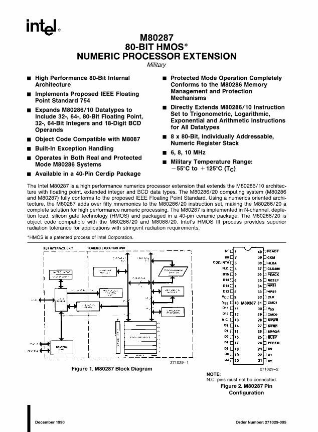
The Intel M80287 is a high performance numerics processor extension that extends the M80286/10 architec-ture with floating point, extended integer and BCD data types. The M80286/20 computing system (M80286and M80287) fully conforms to the proposed IEEE Floating Point Standard. Using a numerics oriented archi-tecture, the M80287 adds over fifty mnemonics to the M80286/20 instruction set, making the M80286/20 acomplete solution for high performance numeric processing. The M80287 is implemented in N-channel, deple-tion load, silicon gate technology (HMOS) and packaged in a 40-pin ceramic package. The M80286/20 isobject code compatible with the M80286/20 and M8088/20. Intel’s HMOS III process provides superiorradiation tolerance for applications with stringent radiation requirements.
*HMOS is a patented process of Intel Corporation.
271029–1
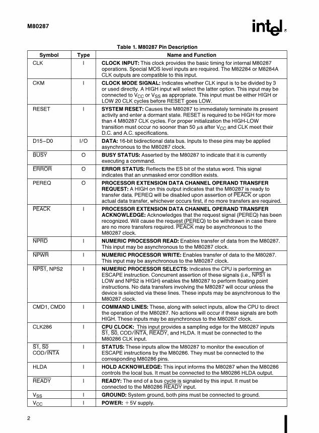
Figure 1. M80287 Block Diagram 271029–2
NOTE:N.C. pins must not be connected.
Figure 2. M80287 Pin
Configuration
M80287
Table 1. M80287 Pin Description
Symbol Type Name and Function
CLK I CLOCK INPUT: This clock provides the basic timing for internal M80287operations. Special MOS level inputs are required. The M82284 or M8284ACLK outputs are compatible to this input.
CKM I CLOCK MODE SIGNAL: Indicates whether CLK input is to be divided by 3or used directly. A HIGH input will select the latter option. This input may beconnected to VCC or VSS as appropriate. This input must be either HIGH orLOW 20 CLK cycles before RESET goes LOW.
RESET I SYSTEM RESET: Causes the M80287 to immediately terminate its presentactivity and enter a dormant state. RESET is required to be HIGH for morethan 4 M80287 CLK cycles. For proper initialization the HIGH-LOWtransition must occur no sooner than 50 ms after VCC and CLK meet theirD.C. and A.C. specifications.
D15–D0 I/O DATA: 16-bit bidirectional data bus. Inputs to these pins may be appliedasynchronous to the M80287 clock.
BUSY O BUSY STATUS: Asserted by the M80287 to indicate that it is currentlyexecuting a command.
ERROR O ERROR STATUS: Reflects the ES bit of the status word. This signalindicates that an unmasked error condition exists.
PEREQ O PROCESSOR EXTENSION DATA CHANNEL OPERAND TRANSFERREQUEST: A HIGH on this output indicates that the M80287 is ready totransfer data. PEREQ will be disabled upon assertion of PEACK or uponactual data transfer, whichever occurs first, if no more transfers are required.
PEACK I PROCESSOR EXTENSION DATA CHANNEL OPERAND TRANSFERACKNOWLEDGE: Acknowledges that the request signal (PEREQ) has beenrecognized. Will cause the request (PEREQ) to be withdrawn in case thereare no more transfers required. PEACK may be asynchronous to theM80287 clock.
NPRD I NUMERIC PROCESSOR READ: Enables transfer of data from the M80287.This input may be asynchronous to the M80287 clock.
NPWR I NUMERIC PROCESSOR WRITE: Enables transfer of data to the M80287.This input may be asynchronous to the M80287 clock.
NPS1, NPS2 I NUMERIC PROCESSOR SELECTS: Indicates the CPU is performing anESCAPE instruction. Concurrent assertion of these signals (i.e., NPS1 isLOW and NPS2 is HIGH) enables the M80287 to perform floating pointinstructions. No data transfers involving the M80287 will occur unless thedevice is selected via these lines. These inputs may be asynchronous to theM80287 clock.
CMD1, CMD0 I COMMAND LINES: These, along with select inputs, allow the CPU to directthe operation of the M80287. No actions will occur if these signals are bothHIGH. These inputs may be asynchronous to the M80287 clock.
CLK286 I CPU CLOCK: This input provides a sampling edge for the M80287 inputsS1, S0, COD/INTA, READY, and HLDA. It must be connected to theM80286 CLK input.
S1, S0 I STATUS: These inputs allow the M80287 to monitor the execution ofCOD/INTA ESCAPE instructions by the M80286. They must be connected to the
corresponding M80286 pins.
HLDA I HOLD ACKNOWLEDGE: This input informs the M80287 when the M80286controls the local bus. It must be connected to the M80286 HLDA output.
READY I READY: The end of a bus cycle is signaled by this input. It must beconnected to the M80286 READY input.
VSS I GROUND: System ground, both pins must be connected to ground.
VCC I POWER: a5V supply.
2
M80287
FUNCTIONAL DESCRIPTION
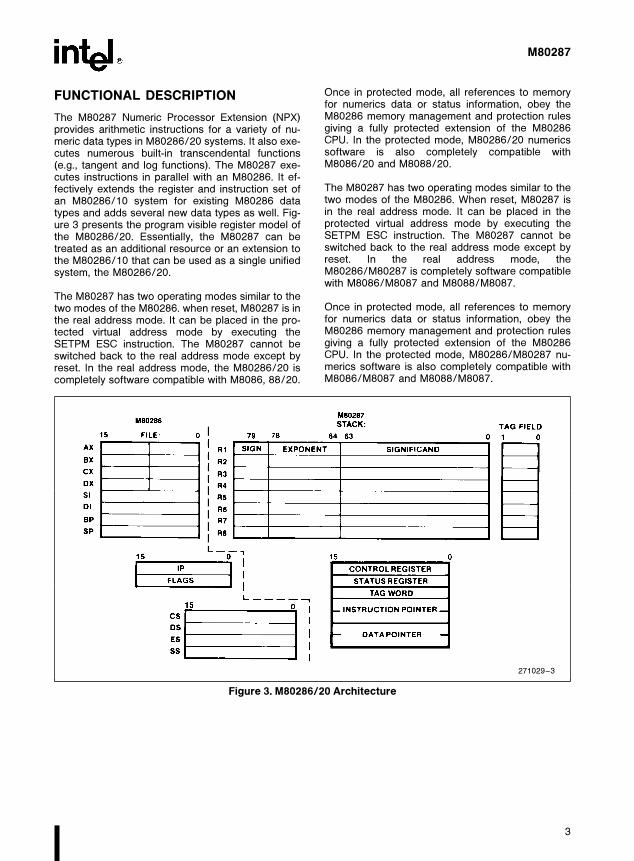
The M80287 Numeric Processor Extension (NPX)provides arithmetic instructions for a variety of nu-meric data types in M80286/20 systems. It also exe-cutes numerous built-in transcendental functions(e.g., tangent and log functions). The M80287 exe-cutes instructions in parallel with an M80286. It ef-fectively extends the register and instruction set ofan M80286/10 system for existing M80286 datatypes and adds several new data types as well. Fig-ure 3 presents the program visible register model ofthe M80286/20. Essentially, the M80287 can betreated as an additional resource or an extension tothe M80286/10 that can be used as a single unifiedsystem, the M80286/20.
The M80287 has two operating modes similar to thetwo modes of the M80286. when reset, M80287 is inthe real address mode. It can be placed in the pro-tected virtual address mode by executing theSETPM ESC instruction. The M80287 cannot beswitched back to the real address mode except byreset. In the real address mode, the M80286/20 iscompletely software compatible with M8086, 88/20.
Once in protected mode, all references to memoryfor numerics data or status information, obey theM80286 memory management and protection rulesgiving a fully protected extension of the M80286CPU. In the protected mode, M80286/20 numericssoftware is also completely compatible withM8086/20 and M8088/20.
The M80287 has two operating modes similar to thetwo modes of the M80286. When reset, M80287 isin the real address mode. It can be placed in theprotected virtual address mode by executing theSETPM ESC instruction. The M80287 cannot beswitched back to the real address mode except byreset. In the real address mode, theM80286/M80287 is completely software compatiblewith M8086/M8087 and M8088/M8087.
Once in protected mode, all references to memoryfor numerics data or status information, obey theM80286 memory management and protection rulesgiving a fully protected extension of the M80286CPU. In the protected mode, M80286/M80287 nu-merics software is also completely compatible withM8086/M8087 and M8088/M8087.
271029–3
Figure 3. M80286/20 Architecture
3
M80287
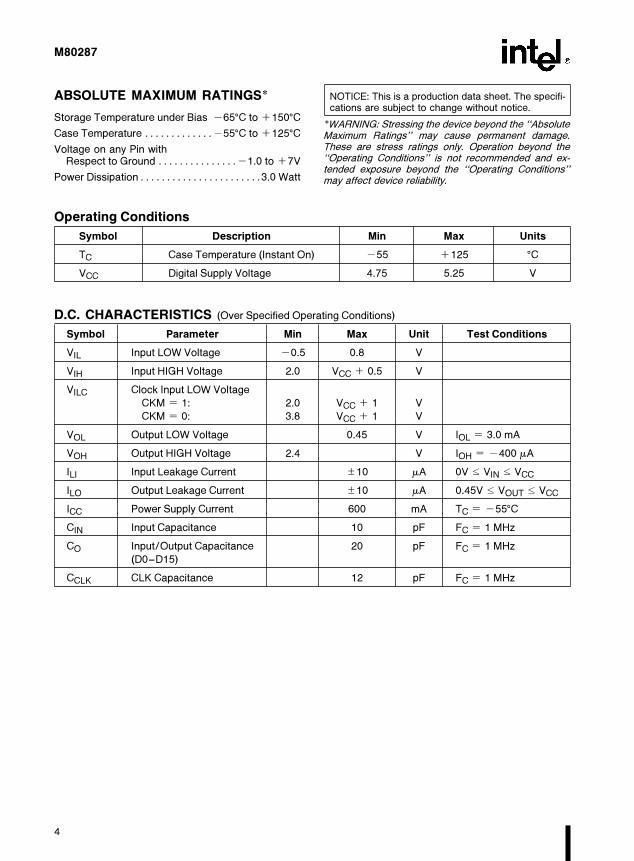
ABSOLUTE MAXIMUM RATINGS*
Storage Temperature under Bias b65§C to a150§CCase Temperature ÀÀÀÀÀÀÀÀÀÀÀÀÀb55§C to a125§CVoltage on any Pin with
Respect to Ground ÀÀÀÀÀÀÀÀÀÀÀÀÀÀÀb1.0 to a7V
Power DissipationÀÀÀÀÀÀÀÀÀÀÀÀÀÀÀÀÀÀÀÀÀÀÀ3.0 Watt
NOTICE: This is a production data sheet. The specifi-cations are subject to change without notice.
*WARNING: Stressing the device beyond the ‘‘AbsoluteMaximum Ratings’’ may cause permanent damage.These are stress ratings only. Operation beyond the‘‘Operating Conditions’’ is not recommended and ex-tended exposure beyond the ‘‘Operating Conditions’’may affect device reliability.
Operating Conditions
Symbol Description Min Max Units
TC Case Temperature (Instant On) b55 a125 §CVCC Digital Supply Voltage 4.75 5.25 V
D.C. CHARACTERISTICS (Over Specified Operating Conditions)
Symbol Parameter Min Max Unit Test Conditions
VIL Input LOW Voltage b0.5 0.8 V
VIH Input HIGH Voltage 2.0 VCC a 0.5 V
VILC Clock Input LOW Voltage
CKM e 1: 2.0 VCC a 1 V
CKM e 0: 3.8 VCC a 1 V
VOL Output LOW Voltage 0.45 V IOL e 3.0 mA
VOH Output HIGH Voltage 2.4 V IOH e b400 mA
ILI Input Leakage Current g10 mA 0V s VIN s VCC
ILO Output Leakage Current g10 mA 0.45V s VOUT s VCC
ICC Power Supply Current 600 mA TC e b55§CCIN Input Capacitance 10 pF FC e 1 MHz
CO Input/Output Capacitance 20 pF FC e 1 MHz
(D0–D15)
CCLK CLK Capacitance 12 pF FC e 1 MHz
4
M80287
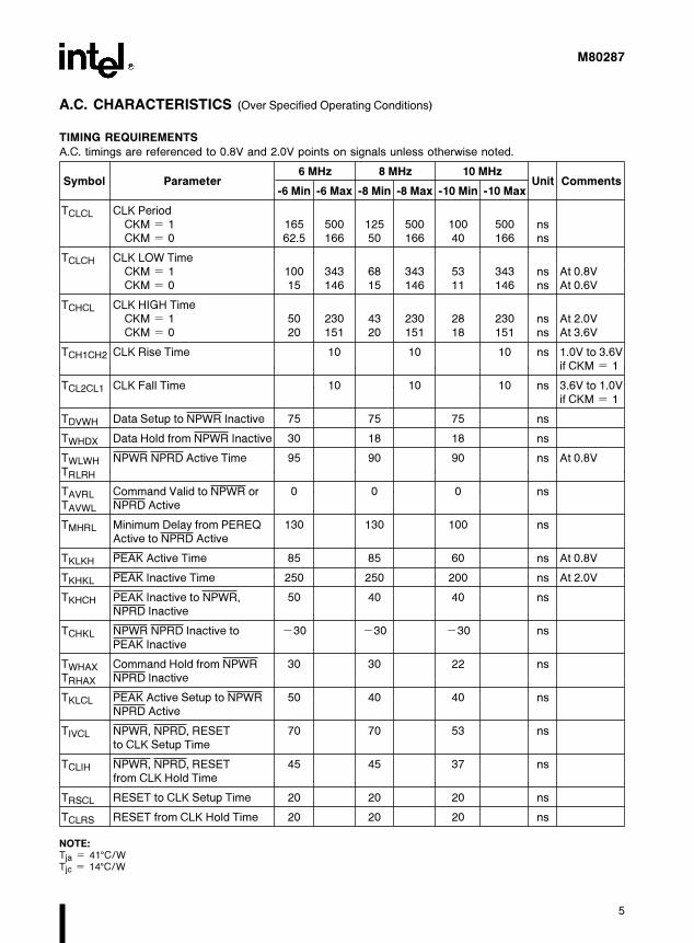
A.C. CHARACTERISTICS (Over Specified Operating Conditions)
TIMING REQUIREMENTS
A.C. timings are referenced to 0.8V and 2.0V points on signals unless otherwise noted.
Symbol Parameter6 MHz 8 MHz 10 MHz
Unit Comments-6 Min -6 Max -8 Min -8 Max -10 Min -10 Max
TCLCL CLK PeriodCKM e 1 165 500 125 500 100 500 nsCKM e 0 62.5 166 50 166 40 166 ns
TCLCH CLK LOW TimeCKM e 1 100 343 68 343 53 343 ns At 0.8VCKM e 0 15 146 15 146 11 146 ns At 0.6V
TCHCL CLK HIGH TimeCKM e 1 50 230 43 230 28 230 ns At 2.0VCKM e 0 20 151 20 151 18 151 ns At 3.6V
TCH1CH2 CLK Rise Time 10 10 10 ns 1.0V to 3.6Vif CKM e 1
TCL2CL1 CLK Fall Time 10 10 10 ns 3.6V to 1.0Vif CKM e 1
TDVWH Data Setup to NPWR Inactive 75 75 75 ns
TWHDX Data Hold from NPWR Inactive 30 18 18 ns
TWLWH NPWR NPRD Active Time 95 90 90 ns At 0.8VTRLRH
TAVRL Command Valid to NPWR or 0 0 0 nsTAVWL NPRD Active
TMHRL Minimum Delay from PEREQ 130 130 100 nsActive to NPRD Active
TKLKH PEAK Active Time 85 85 60 ns At 0.8V
TKHKL PEAK Inactive Time 250 250 200 ns At 2.0V
TKHCH PEAK Inactive to NPWR, 50 40 40 nsNPRD Inactive
TCHKL NPWR NPRD Inactive to b30 b30 b30 nsPEAK Inactive
TWHAX Command Hold from NPWR 30 30 22 nsTRHAX NPRD Inactive
TKLCL PEAK Active Setup to NPWR 50 40 40 nsNPRD Active
TIVCL NPWR, NPRD, RESET 70 70 53 nsto CLK Setup Time
TCLIH NPWR, NPRD, RESET 45 45 37 nsfrom CLK Hold Time
TRSCL RESET to CLK Setup Time 20 20 20 ns
TCLRS RESET from CLK Hold Time 20 20 20 ns
NOTE:Tja e 41§C/WTjc e 14§C/W
5
M80287
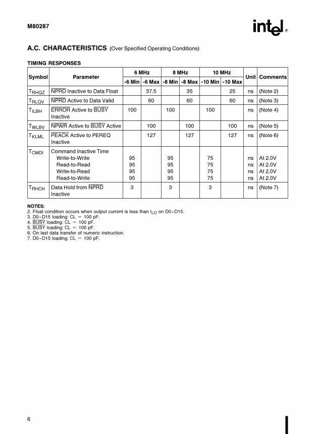
A.C. CHARACTERISTICS (Over Specified Operating Conditions)
TIMING RESPONSES
Symbol Parameter6 MHz 8 MHz 10 MHz
Unit Comments-6 Min -6 Max -8 Min -8 Max -10 Min -10 Max
TRHQZ NPRD Inactive to Data Float 37.5 35 25 ns (Note 2)
TRLQV NPRD Active to Data Valid 60 60 60 ns (Note 3)
TILBH ERROR Active to BUSY 100 100 100 ns (Note 4)
Inactive
TWLBV NPWR Active to BUSY Active 100 100 100 ns (Note 5)
TKLML PEACK Active to PEREQ 127 127 127 ns (Note 6)
Inactive
TCMDI Command Inactive Time
Write-to-Write 95 95 75 ns At 2.0V
Read-to-Read 95 95 75 ns At 2.0V
Write-to-Read 95 95 75 ns At 2.0V
Read-to-Write 95 95 75 ns At 2.0V
TRHCH Data Hold from NPRD 3 3 3 ns (Note 7)
Inactive
NOTES:2. Float condition occurs when output current is less than ILO on D0–D15.3. D0–D15 loading: CL e 100 pF.4. BUSY loading: CL e 100 pF.5. BUSY loading: CL e 100 pF.6. On last data transfer of numeric instruction.7. D0–D15 loading: CL e 100 pF.
6
M80287
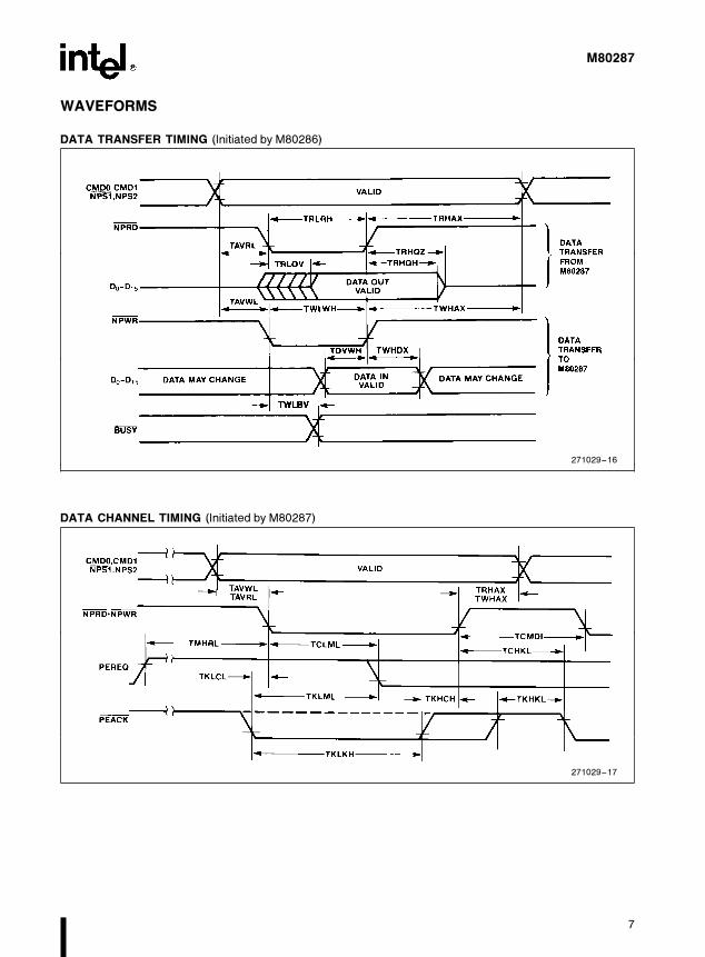
WAVEFORMS
DATA TRANSFER TIMING (Initiated by M80286)
271029–16
DATA CHANNEL TIMING (Initiated by M80287)
271029–17
7
M80287
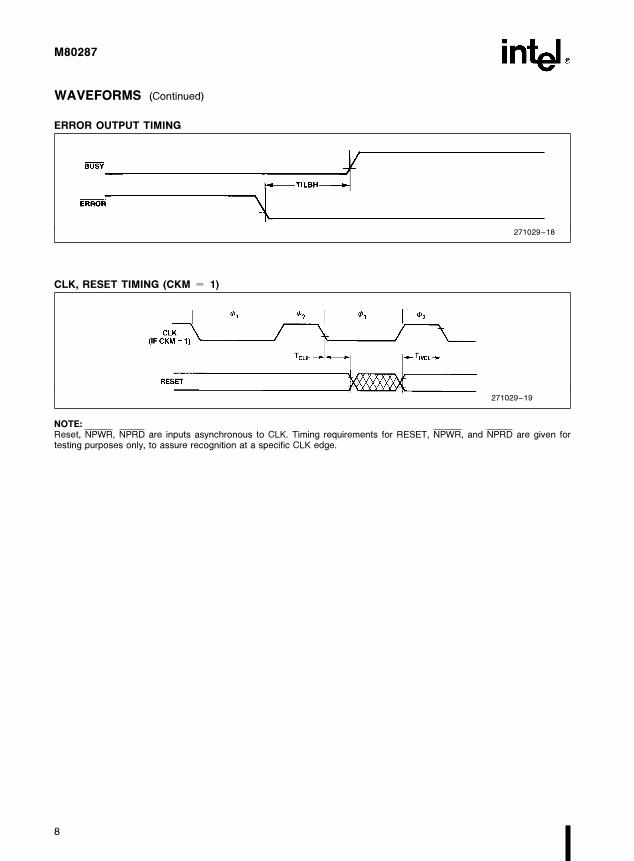
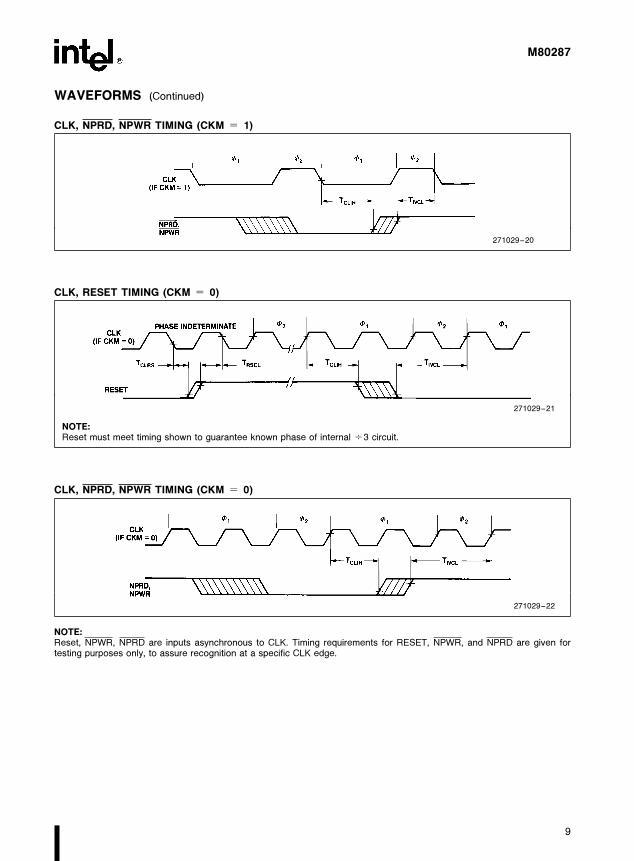
WAVEFORMS (Continued)
ERROR OUTPUT TIMING
271029–18
CLK, RESET TIMING (CKM e 1)
271029–19
NOTE:Reset, NPWR, NPRD are inputs asynchronous to CLK. Timing requirements for RESET, NPWR, and NPRD are given fortesting purposes only, to assure recognition at a specific CLK edge.
8
M80287
WAVEFORMS (Continued)
CLK, NPRD, NPWR TIMING (CKM e 1)
271029–20
CLK, RESET TIMING (CKM e 0)
271029–21
NOTE:Reset must meet timing shown to guarantee known phase of internal d3 circuit.
CLK, NPRD, NPWR TIMING (CKM e 0)
271029–22
NOTE:Reset, NPWR, NPRD are inputs asynchronous to CLK. Timing requirements for RESET, NPWR, and NPRD are given fortesting purposes only, to assure recognition at a specific CLK edge.
9
M80287
WAVEFORMS (Continued)
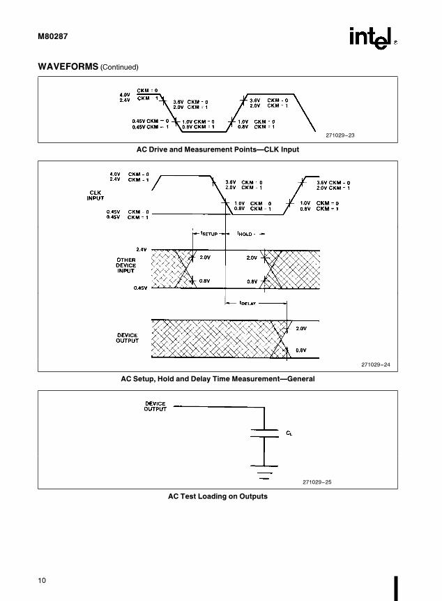
271029–23
AC Drive and Measurement PointsÐCLK Input
271029–24
AC Setup, Hold and Delay Time MeasurementÐGeneral
271029–25
AC Test Loading on Outputs
10
M80287
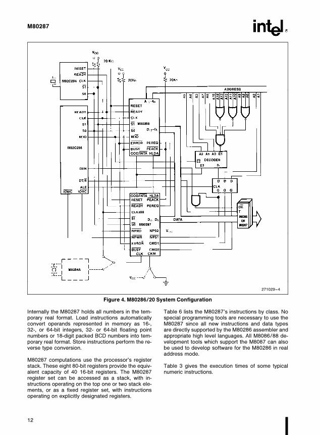
SYSTEM CONFIGURATION WITHM80286
As a processor extension to an M80286, theM80287 can be connected to the CPU as shown inFigure 4. The data channel control signals (PEREQ,PEACK), the BUSY signal and the NPRD, NPWRsignals, allow the NPX to receive instructions anddata from the CPU. When in the protected mode, allinformation received by the NPX is validated by theM80286 memory management and protection unit.Once started, the M80287 can process in parallelwith and independent of the host CPU. When theNPX detects an error or exception, it will indicate thisto the CPU by asserting the ERROR signal.
The NPX uses the processor extension request andacknowledge pins of the M80286 CPU to implementdata transfers with memory under the protectionmodel of the CPU. The full virtual and physical ad-dress space of the M80286 is available. Data for theM80287 in memory is addressed and represented inthe same manner as for an M8087.
The M80287 can operate either directly from theCPU clock or with a dedicated clock. For operationwith the CPU clock (CKM e 0), the M80287 worksat one-third the frequency of the system clock (i.e.,for an 8 MHz M80286, the 16 MHz system clock isdivided down to 5.3 MHz). The M80287 provides acapability to internally divide the CPU clock by threeto produce the required internal clock (33% duty cy-cle). To use a higher performance M80287 (8 MHz),an M8284A clock driver and appropriate crystal maybe used to directly drive the M80287 with a (/3 dutycycle clock on the CLK input (CKM e 1).
SYSTEM CONFIGURATION WITHM80386
The M80287 can also be connected as a processorextension to the M80386 CPU as shown in Figure4b. All software written for M8086/M8087 andM80286/M80287 is object code compatible with80386/M80287 and can benefit from the increasedspeed of the M80386 CPU.
Note that the PEACK input pin is pulled high. This isbecause the M80287 is not required to keep track ofthe number of words transferred during an operandtransfer when it is connected to the M80386 CPU.Unlike the M80286 CPU, the M80386 CPU knowsthe exact length of the operand being transferredto/from the M80287. After an ESC instruction hasbeen sent to the M80287, the M80386 processorextension data channel will initiate the data transferas soon as it receives the PEREQ signal from theM80287. The transfer is automatically terminated bythe M80386 CPU as soon as all the words of theoperand have been transferred.
Because of the very high speed local bus of theM80386 CPU, the M80287 cannot reside directly onthe CPU local bus. A local bus controller logic isused to generate the necessary read and write cycletiming as well as the chip select timings for theM80287. The M80386 CPU uses I/O addresses800000F8 through 800000FF to communicate withthe M80287. This is beyond the normal I/O addressspace of the CPU and makes it easier to generatethe chip select signals using A31 and M/IO. It mayalso be noted that the M80386 CPU automaticallygenerates 16-bit bus cycles whenever it communi-cates with the M80287.
HARDWARE INTERFACE
Communication of instructions and data operandsbetween the M80286 and M80287 is handled by theCMD0, CMD1, NPS1, NPS2, NPRD, and NPWR sig-nals. I/O port addresses 00F8H, 00FAH, and 00FCHare used by the M80286 for this communication.When any of these addresses are used, the NPS1input must be LOW and NPS2 input HIGH. TheIORC and IOWC outputs of the M82288 identify I/Ospace transfers (see Figure 4). CMD0 should beconnected to latched M80286 A1 and CMD1 shouldbe connected to latched M80286 A2.
I/O ports 00F8H to 00FFH are reserved for theM80286/M80287 interface. To guarantee correctoperation of the M80287, programs must not per-form any I/O operations to these ports.
The PEREQ, PEACK, BUSY, and ERROR signals ofthe M80287 are connected to the same-namedM80286 input. The data pins of the M80287 shouldbe directly connected to the M80286 data bus. Notethat all bus drivers connected to the M80286 localbus must be inhibited when the M80286 reads fromthe M80287. The use of COD/INTA and M/IO in thedecoder prevents INTA bus cycles from disablingthe data transceivers.
The S1, S0, COD/INTA, READY, HLDA, and CLKpins of the M80286 are connected to the samenamed pins on the M80287. These signals allow theM80287 to monitor the execution of ESCAPE in-structions by the M80826.
PROGRAMMING INTERFACE
Table 2 lists the seven data types the M80287 sup-ports and presents the format for each type. Thesevalues are stored in memory with the least signifi-cant digits at the lowest memory address. Programsretrieve these values by generating the lowest ad-dress. All values should start at even addresses formaximum system performance.
11
M80287
271029–4
Figure 4. M80286/20 System Configuration
Internally the M80287 holds all numbers in the tem-porary real format. Load instructions automaticallyconvert operands represented in memory as 16-,32-, or 64-bit integers, 32- or 64-bit floating pointnumbers or 18-digit packed BCD numbers into tem-porary real format. Store instructions perform the re-verse type conversion.
M80287 computations use the processor’s registerstack. These eight 80-bit registers provide the equiv-alent capacity of 40 16-bit registers. The M80287register set can be accessed as a stack, with in-structions operating on the top one or two stack ele-ments, or as a fixed register set, with instructionsoperating on explicitly designated registers.
Table 6 lists the M80287’s instructions by class. Nospecial programming tools are necessary to use theM80287 since all new instructions and data typesare directly supported by the M80286 assembler andappropriate high level languages. All M8086/88 de-velopment tools which support the M8087 can alsobe used to develop software for the M80286 in realaddress mode.
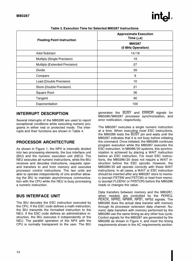
Table 3 gives the execution times of some typicalnumeric instructions.
12

M80287
Table 2. M80287 Datatype Representation in Memory
271029–5
NOTES:1. S e Sign bit (0 e positive, 1 e negative)2. dn e Decimal digit (two per byte)3. X e Bits have no significance; M8087 ignores when loading, zeros when storing.4. U e Position of implicit binary point5. I e Integer bit of significand; stored in temporary real, implicit in short and long real.6. Exponent Bias (normalized values):
Short Real: 127 (7FH)Long Real: 1023 (3FFH)Temporary Real: 16383 (3FFFH)
7. Packed BCD: (b1)S (D17 . . . D0)8. Real: (b1)S (2E-BIAS) (F0 F1 . . . )
SOFTWARE INTERFACE
The M80286/20 is programmed as a single proces-sor. All communication between the M80286 andthe M80287 is transparent to software. The CPU au-tomatically controls the M80287 whenever a numer-ic instruction is executed. All memory addressingmodes, physical memory, and virtual memory of theCPU are available for use by the NPX.
Since the NPX operates in parallel with the CPU, anyerrors detected by the NPX may be reported afterthe CPU has executed the ESCAPE instructionwhich caused it. To allow identification of the failingnumeric instruction, the NPX contains two pointerregisters which identify the address of the failing nu-meric instruction and the numeric memory operand ifappropriate for the instruction encountering this er-ror.
13
M80287
Table 3. Execution Time for Selected M80287 Instructions
Approximate Execution
Floating Point InstructionTime (ms)
M80287
(5 MHz Operation)
Add/Subtract 14/18
Multiply (Single Precision) 19
Multiply (Extended Precision) 27
Divide 39
Compare 9
Load (Double Precision) 10
Store (Double Precision) 21
Square Root 36
Tangent 90
Exponentiation 100
INTERRUPT DESCRIPTION
Several interrupts of the M80286 are used to reportexceptional conditions while executing numeric pro-grams in either real or protected mode. The inter-rupts and their functions are shown in Table 4.
PROCESSOR ARCHITECTURE
As shown in Figure 1, the NPX is internally dividedinto two processing elements, the bus interface unit(BIU) and the numeric execution unit (NEU). TheNEU executes all numeric instructions, while the BIUreceives and decodes instructions, requests oper-and transfers to and from memory and executesprocessor control instructions. The two units areable to operate independently of one another allow-ing the BIU to maintain asynchronous communica-tion with the CPU while the NEU is busy processinga numeric instruction.
BUS INTERFACE UNIT
The BIU decodes the ESC instruction executed bythe CPU. If the ESC code defines a math instruction,the BIU transmits the formatted instruction to theNEU. If the ESC code defines an administrative in-struction, the BIU executes it independently of theNEU. The parallel operation of the NPX with theCPU is normally transparent to the user. The BIU
generates the BUSY and ERROR signals forM80286/M80287 processor synchronization, anderror notification, respectively.
The M80287 executes a single numeric instructionat a time. When executing most ESC instructions,the M80286 tests the BUSY pin and waits until theM80287 indicates that it is not busy before initiatingthe command. Once initiated, the M80286 continuesprogram execution while the M80287 executes theESC instruction. In M8086/20 systems, this synchro-nization is achieved by placing a WAIT instructionbefore an ESC instruction. For most ESC instruc-tions, the M80286/20 does not require a WAIT in-struction before the ESC opcode. However, theM80286/20 will operate correctly with these WAITinstructions. In all cases, a WAIT or ESC instructionshould be inserted after any M80287 store to memo-ry (except FSTSW and FSTCW) or load from memo-ry (except FLDENV or FRSTOR) before the M80286reads or changes the value.
Data transfers between memory and the M80287,when needed, are controlled by the PEREQ,PEACK, NPRD, NPWR, NPS1, NPS2 signals. TheM80286 does the actual data transfer with memorythrough its processor extension data channel. Nu-meric data transfers with memory performed by theM80286 use the same timing as any other bus cycle.Control signals for the M80287 are generated by theM80286 as shown in Figure 4, and meet the timingrequirements shown in the AC requirements section.
14
M80287
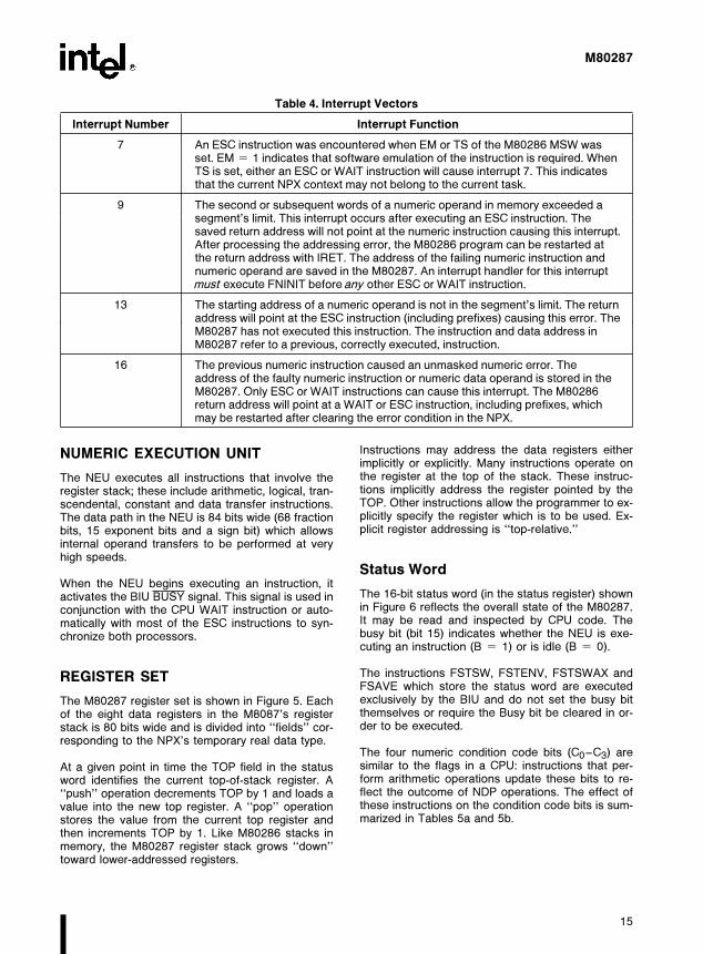
Table 4. Interrupt Vectors
Interrupt Number Interrupt Function
7 An ESC instruction was encountered when EM or TS of the M80286 MSW wasset. EM e 1 indicates that software emulation of the instruction is required. WhenTS is set, either an ESC or WAIT instruction will cause interrupt 7. This indicatesthat the current NPX context may not belong to the current task.
9 The second or subsequent words of a numeric operand in memory exceeded asegment’s limit. This interrupt occurs after executing an ESC instruction. Thesaved return address will not point at the numeric instruction causing this interrupt.After processing the addressing error, the M80286 program can be restarted atthe return address with IRET. The address of the failing numeric instruction andnumeric operand are saved in the M80287. An interrupt handler for this interruptmust execute FNINIT beforeany other ESC or WAIT instruction.
13 The starting address of a numeric operand is not in the segment’s limit. The returnaddress will point at the ESC instruction (including prefixes) causing this error. TheM80287 has not executed this instruction. The instruction and data address inM80287 refer to a previous, correctly executed, instruction.
16 The previous numeric instruction caused an unmasked numeric error. Theaddress of the faulty numeric instruction or numeric data operand is stored in theM80287. Only ESC or WAIT instructions can cause this interrupt. The M80286return address will point at a WAIT or ESC instruction, including prefixes, whichmay be restarted after clearing the error condition in the NPX.
NUMERIC EXECUTION UNIT
The NEU executes all instructions that involve theregister stack; these include arithmetic, logical, tran-scendental, constant and data transfer instructions.The data path in the NEU is 84 bits wide (68 fractionbits, 15 exponent bits and a sign bit) which allowsinternal operand transfers to be performed at veryhigh speeds.
When the NEU begins executing an instruction, itactivates the BIU BUSY signal. This signal is used inconjunction with the CPU WAIT instruction or auto-matically with most of the ESC instructions to syn-chronize both processors.
REGISTER SET
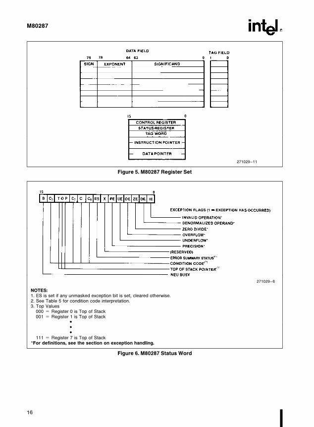
The M80287 register set is shown in Figure 5. Eachof the eight data registers in the M8087’s registerstack is 80 bits wide and is divided into ‘‘fields’’ cor-responding to the NPX’s temporary real data type.
At a given point in time the TOP field in the statusword identifies the current top-of-stack register. A‘‘push’’ operation decrements TOP by 1 and loads avalue into the new top register. A ‘‘pop’’ operationstores the value from the current top register andthen increments TOP by 1. Like M80286 stacks inmemory, the M80287 register stack grows ‘‘down’’toward lower-addressed registers.
Instructions may address the data registers eitherimplicitly or explicitly. Many instructions operate onthe register at the top of the stack. These instruc-tions implicitly address the register pointed by theTOP. Other instructions allow the programmer to ex-plicitly specify the register which is to be used. Ex-plicit register addressing is ‘‘top-relative.’’
Status Word
The 16-bit status word (in the status register) shownin Figure 6 reflects the overall state of the M80287.It may be read and inspected by CPU code. Thebusy bit (bit 15) indicates whether the NEU is exe-cuting an instruction (B e 1) or is idle (B e 0).
The instructions FSTSW, FSTENV, FSTSWAX andFSAVE which store the status word are executedexclusively by the BIU and do not set the busy bitthemselves or require the Busy bit be cleared in or-der to be executed.
The four numeric condition code bits (C0–C3) aresimilar to the flags in a CPU: instructions that per-form arithmetic operations update these bits to re-flect the outcome of NDP operations. The effect ofthese instructions on the condition code bits is sum-marized in Tables 5a and 5b.
15
M80287
271029–11
Figure 5. M80287 Register Set
271029–6
NOTES:1. ES is set if any unmasked exception bit is set, cleared otherwise.2. See Table 5 for condition code interpretation.3. Top Values
000 e Register 0 is Top of Stack001 e Register 1 is Top of Stack
###
111 e Register 7 is Top of Stack*For definitions, see the section on exception handling.
Figure 6. M80287 Status Word
16

M80287
Bits 14–12 of the status word point to the M80287register that is the current top-of-stack (TOP) as de-scribed above. Figure 6 shows the six error flags inbits 5–0 of the status word. Bits 5–0 are set to indi-cate that the NEU has detected an exception whileexecuting an instruction. The section on exceptionhandling explains how they are set and used.
Bit 7 is the error status bit. This bit is set if any un-masked exception bit is set and cleared otherwise. Ifthis bit is set, the ERROR signal is asserted.
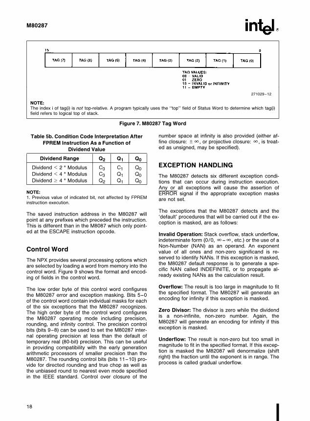
Tag Word
The tag word marks the content of each register asshown in Figure 7. The principal function of the tagword is to optimize the NPX’s performance. The tagword can be used, however, to interpret the con-tents of M80287 registers.
Instruction and Data Pointers
The instruction and data pointers (see Figures 8aand 8b) are provided for user-written error handlers.Whenever the M80287 executes a new instruction,the BIU saves the instruction address, the operandaddress (if present) and the instruction opcode.M80287 instructions can store this data into memo-ry.
The instruction and data pointers appear in one oftwo formats depending on the operating mode of theM80287. In real mode, these values are the 20-bitphysical address and 11-bit opcode formatted likethe M8087. In protected mode, these values are the32-bit virtual addresses used by the program whichexecuted an ESC instruction. The same FLDENV/FSTENV/FSAVE/FRSTOR instructions as those ofthe M8087 are used to transfer these values be-tween the M80287 registers and memory.
Table 5a. Condition Code Interpretation
InstructionC3 C2 C1 C0 Interpretation
Type
Compare, Test 0 0 X 0 ST l Source or 0 (FTST)
0 0 X 1 ST k Source or 0 (FTST)
1 0 X 0 ST e Source or 0 (FTST)
1 1 X 1 ST is not comparable
Remainder Q1 0 Q0 Q2 Complete reduction with
three low bits of quotient
(See Table 5b)
U 1 U U Incomplete Reduction
Examine 0 0 0 0 Valid, positive unnormalized
0 0 0 1 Invalid, positive, exponent e 0
0 0 1 0 Valid, negative, unnormalized
0 0 1 1 Invalid, negative, exponent e 0
0 1 0 0 Valid, positive, normalized
0 1 0 1 Infinity, positive
0 1 1 0 Valid, negative, normalized
0 1 1 1 Infinity, negative
1 0 0 0 Zero, positive
1 0 0 1 Empty
1 0 1 0 Zero, negative
1 0 1 1 Empty
1 1 0 0 Invalid, positive, exponent e 0
1 1 0 1 Empty
1 1 1 0 Invalid, negative, exponent e 0
1 1 1 1 Empty
NOTES:1. ST e Top of stack2. X e value is not affected by instruction3. U e value is undefined following instruction4. Qn e Quotient bit n
17
M80287
271029–12
NOTE:The index i of tag(i) is not top-relative. A program typically uses the ‘‘top’’ field of Status Word to determine which tag(i)field refers to logical top of stack.
Figure 7. M80287 Tag Word
Table 5b. Condition Code Interpretation After
FPREM Instruction As a Function of
Dividend Value
Dividend Range Q2 Q1 Q0
Dividend k 2 * Modulus C3 C1 Q0
Dividend k 4 * Modulus C3 Q1 Q0
Dividend t 4 * Modulus Q2 Q1 Q0
NOTE:1. Previous value of indicated bit, not affected by FPREMinstruction execution.
The saved instruction address in the M80287 willpoint at any prefixes which preceded the instruction.This is different than in the M8087 which only point-ed at the ESCAPE instruction opcode.
Control Word
The NPX provides several processing options whichare selected by loading a word from memory into thecontrol word. Figure 9 shows the format and encod-ing of fields in the control word.
The low order byte of this control word configuresthe M80287 error and exception masking. Bits 5–0of the control word contain individual masks for eachof the six exceptions that the M80287 recognizes.The high order byte of the control word configuresthe M80287 operating mode including precision,rounding, and infinity control. The precision controlbits (bits 9–8) can be used to set the M80287 inter-nal operating precision at less than the default oftemporary real (80-bit) precision. This can be usefulin providing compatibility with the early generationarithmetic processors of smaller precision than theM80287. The rounding control bits (bits 11–10) pro-vide for directed rounding and true chop as well asthe unbiased round to nearest even mode specifiedin the IEEE standard. Control over closure of the
number space at infinity is also provided (either af-fine closure: g%, or projective closure: %, is treat-ed as unsigned, may be specified).
EXCEPTION HANDLING
The M80287 detects six different exception condi-tions that can occur during instruction execution.Any or all exceptions will cause the assertion ofERROR signal if the appropriate exception masksare not set.
The exceptions that the M80287 detects and the‘default’ procedures that will be carried out if the ex-ception is masked, are as follows:
Invalid Operation: Stack overflow, stack underflow,indeterminate form (0/0, % –%, etc.) or the use of aNon-Number (NAN) as an operand. An exponentvalue of all ones and non-zero significand is re-served to identify NANs. If this exception is masked,the M80287 default response is to generate a spe-cific NAN called INDEFINITE, or to propagate al-ready existing NANs as the calculation result.
Overflow: The result is too large in magnitude to fitthe specified format. The M80287 will generate anencoding for infinity if this exception is masked.
Zero Divisor: The divisor is zero while the dividendis a non-infinite, non-zero number. Again, theM80287 will generate an encoding for infinity if thisexception is masked.
Underflow: The result is non-zero but too small inmagnitude to fit in the specified format. If this excep-tion is masked the M82087 will denormalize (shiftright) the fraction until the exponent is in range. Theprocess is called gradual underflow.
18

M80287
271029–13
Figure 8a. Protected Mode Instruction and Data Pointer Image in Memory
Denormalized Operand: At least one of the oper-ands is denormalized; it has the smallest exponentbut a non-zero significand. Normal processing con-tinues if this exception is masked off.
Inexact Result: If the true result is not exactly repre-sentable in the specified format, the result is round-ed according to the rounding mode, and this flag isset. If this exception is masked, processing will sim-ply continue.
If the error is not masked, the corresponding errorbit and the error status bit (ES) in the control wordwill be set, and the ERROR output signal will be as-serted. If the CPU attempts to execute another ESCor WAIT instruction, exception 7 will occur.
The error condition must be resolved via an interruptservice routine. The M80287 saves the address ofthe floating point instruction causing the error as wellas the address of the lowest memory location of anymemory operand required by that instruction.
M8086/20 COMPATIBILITY
M80286/20 supports portability of M8086/20 pro-grams when it is in the real address mode. However,because of differences in the numeric error handlingtechniques, error handling routines may need to bechanged. The differences between an M80286/20and M8086/20 are:
1. The NPX error signal does not pass through aninterrupt controller (M8087 INT signal does).
Therefore, any interrupt controller oriented instruc-tions for the M8086/20 may have to be deleted.
2. Interrupt vector 16 must point at the numeric errorhandler routine.
3. The saved floating point instruction address in theM80287 includes any leading prefixes before theESCAPE opcode. The corresponding saved addressof the M8087 does not include leading prefixes.
4. In protected mode, the format of the saved in-struction and operand pointers is different than forthe M8087. The instruction opcode is not savedÐitmust be read from memory if needed.
5. Interrupt 7 will occur when executing ESC instruc-tions with either TS or EM of MSW e 1. If TS ofMSW e 1 then WAIT will also cause interrupt 7. Aninterrupt handler should be added to handle this situ-ation.
6. Interrupt 9 will occur if the second or subsequentwords of a floating point operand fall outside a seg-ment’s size. Interrupt 13 will occur if the starting ad-dress of a numeric operand falls outside a seg-ment’s size. An interrupt handler should be added toreport these programming errors.
In the protected mode, M8086/20 application codecan be directly ported via recompilation if the 286memory protection rules are not violated.
19

M80287
271029–14
Figure 8b. Real Mode M80287 Instruction and Data Pointer Image in Memory
271029–7
NOTES:1. Precision Control 2. Rounding Control
00 e 24 Bits (short real) 00 e Round To Nearest Or Even01 e Reserved 01 e Round Down (Toward b%)10 e 53 Bits (long real) 10 e Round Up (Toward a%)11 e 64 Bits (temp real) 11 e Chop (Truncate Toward Zero)
Figure 9. M80287 Control Word
20
M80287
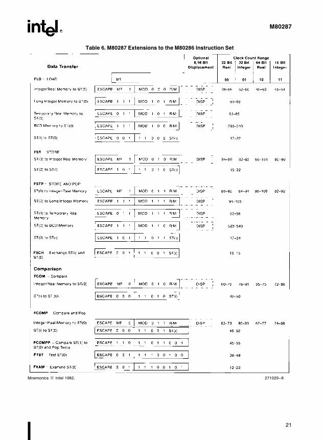
Table 6. M80287 Extensions to the M80286 Instruction Set
Mnemonics © Intel 1982. 271029–8
21

M80287
Table 6. M80287 Extensions to the M80286 Instruction Set (Continued)
271029–9
NOTE:1. If P e 1 then add 5 clocks.
22
M80287
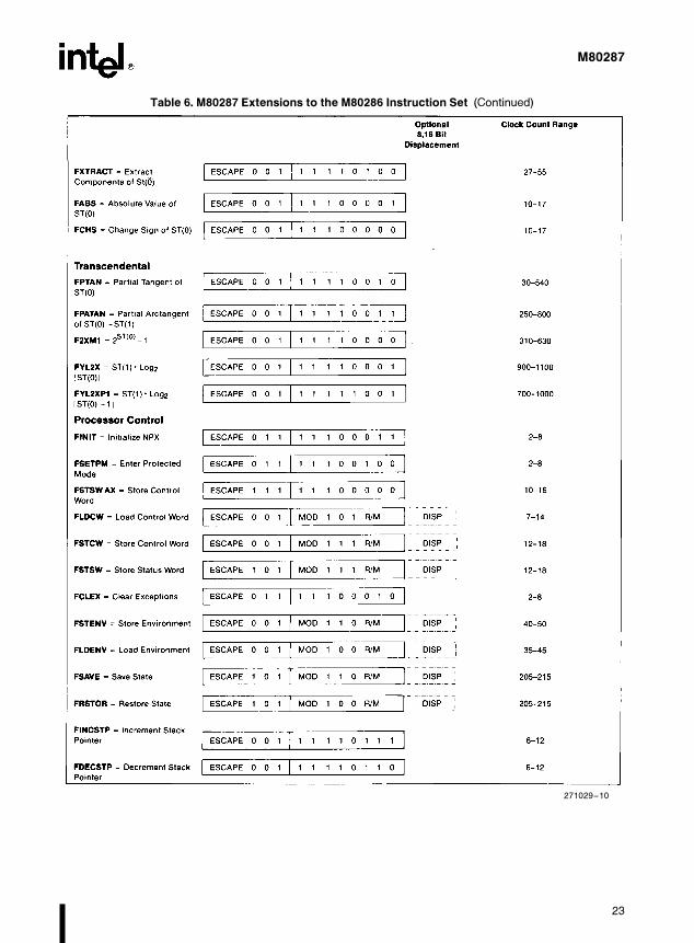
Table 6. M80287 Extensions to the M80286 Instruction Set (Continued)
271029–10
23
M80287
Table 6. M80287 Extensions to the M80286 Instruction Set (Continued)
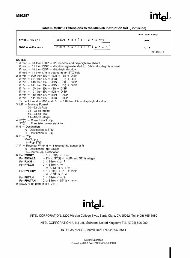
271029–15
NOTES:1. if mod e 00 then DISP e 0*, disp-low and disp-high are absent
if mod e 01 then DISP e disp-low sign-extended to 16-bits, disp-high is absentif mod e 10 then DISP e disp-high; disp-lowif mod e 11 then r/m is treated as an ST(i) field
2. if r/m e 000 then EA e (BX) a (SI) a DISPif r/m e 001 then EA e (BX) a (DI) a DISPif r/m e 010 then EA e (BP) a (SI) a DISPif r/m e 011 then EA e (BP) a (DI) a DISPif r/m e 100 then EA e (SI) a DISPif r/m e 101 then EA e (DI) a DISPif r/m e 110 then EA e (BP) a DISPif r/m e 111 then EA e (BX) a DISP*except if mod e 000 and r/m e 110 then EA e disp-high; disp-low.
3. MF e Memory Format00Ð32-bit Real01Ð32-bit Integer10Ð64-bit Real11Ð16-bit Integer
4. ST(0) e Current stack topST(i) ith register below stack top
5. d e Destination0ÐDestination is ST(0)1ÐDestination is ST(i)
6. P e Pop0ÐNo pop1ÐPop ST(0)
7. R e Reverse: When d e 1 reverse the sense of R0ÐDestination (op) Source1ÐSource (op) Destination
8. For FSQRT: b0 s ST(0) s a%
For FSCALE: b215 s ST(1) k a215 and ST(1) integerFor F2XM1: 0 s ST(0) s 2b1
For FYL2X: 0 k ST(0) k %
b% k ST(1) k a%
For FYL2XP1: 0 s IST(0)I k (2 b S2)/2b% k ST(1) k %
For FPTAN: 0 s ST(0) s q/4For FPATAN: 0 s ST(0) k ST(1) k a%
9. ESCAPE bit pattern is 11011.
INTEL CORPORATION, 2200 Mission College Blvd., Santa Clara, CA 95052; Tel. (408) 765-8080
INTEL CORPORATION (U.K.) Ltd., Swindon, United Kingdom; Tel. (0793) 696 000
INTEL JAPAN k.k., Ibaraki-ken; Tel. 029747-8511
Printed in U.S.A./xxxx/1296/2.5K/RP SM
Military Operation


![T00160030120134077[L] Pert 3 - Operator, Operand, And Arithmetic](https://static.fdocuments.in/doc/165x107/55cf8acf55034654898df54d/t00160030120134077l-pert-3-operator-operand-and-arithmetic.jpg)