M29DW323DT ST Microelectronics FLASH Programmer€¦ · M29DW323DT ST Microelectronics FLASH...
27
M29DW323DT ST Microelectronics FLASH Programmer Ken Chapman A Reference Design for the Spartan-3A Starter Kit Includes a multi-rate UART Xilinx Ltd Rev.1b – 30 th October 2008
Transcript of M29DW323DT ST Microelectronics FLASH Programmer€¦ · M29DW323DT ST Microelectronics FLASH...
M29DW323DT ST Microelectronics FLASH Programmer
Ken Chapman
A Reference Design for the Spartan-3A Starter Kit
Includes a multi-rate UART
Xilinx LtdRev.1b – 30th October 2008

M29DW323DT ST Microelectronics FLASH Programmer 2
LimitationsLimited Warranty and Disclaimer. These designs are provided to you “as is”. Xilinx and its licensors make and you receive no warranties or conditions, express, implied, statutory or otherwise, and Xilinx specifically disclaims any implied warranties of merchantability, non-infringement, or fitness for a particular purpose. Xilinx does not warrant that the functions contained in these designs will meet your requirements, or that the operation of these designs will be uninterrupted or error free, or that defects in the Designs will be corrected. Furthermore, Xilinx does not warrant or make any representations regarding use or the results of the use of the designs in terms of correctness, accuracy, reliability, or otherwise.
Limitation of Liability. In no event will Xilinx or its licensors be liable for any loss of data, lost profits, cost or procurement of substitute goods or services, or for any special, incidental, consequential, or indirect damages arising from the use or operation of the designs or accompanying documentation, however caused and on any theory of liability. This limitation will apply even if Xilinx has been advised of the possibility of such damage. This limitation shall apply not-withstanding the failure of the essential purpose of any limited remedies herein.
This design module is not supported by general Xilinx Technical support as an official Xilinx Product.Please refer any issues initially to the provider of the module.
Any problems or items felt of value in the continued improvement of KCPSM3 or this reference design would be gratefully received by the author.
Ken ChapmanSenior Staff Engineer – Spartan Applications Specialistemail: [email protected]
The author would also be pleased to hear from anyone using KCPSM3 or the UART macros with information about your application and how these macros have been useful.
M29DW323DT ST Microelectronics FLASH Programmer 3
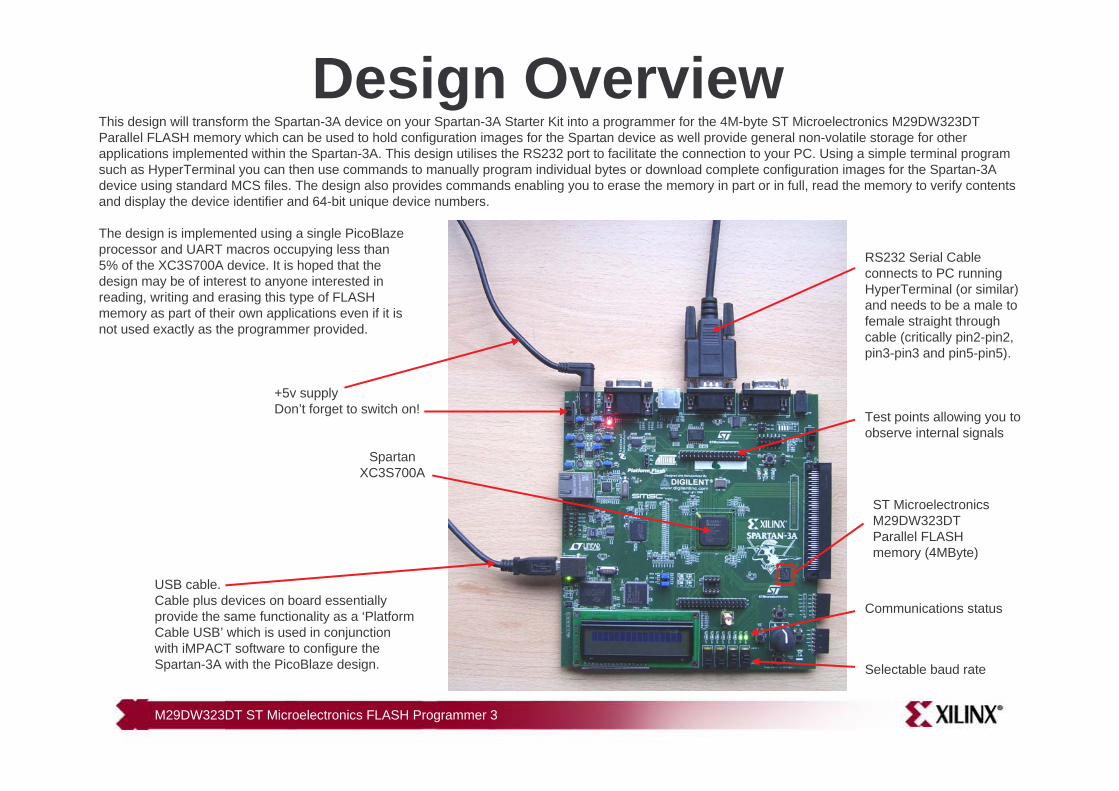
Design OverviewThis design will transform the Spartan-3A device on your Spartan-3A Starter Kit into a programmer for the 4M-byte ST Microelectronics M29DW323DT Parallel FLASH memory which can be used to hold configuration images for the Spartan device as well provide general non-volatile storage for other applications implemented within the Spartan-3A. This design utilises the RS232 port to facilitate the connection to your PC. Using a simple terminal program such as HyperTerminal you can then use commands to manually program individual bytes or download complete configuration images for the Spartan-3A device using standard MCS files. The design also provides commands enabling you to erase the memory in part or in full, read the memory to verify contents and display the device identifier and 64-bit unique device numbers.
ST Microelectronics M29DW323DT Parallel FLASH memory (4MByte)
The design is implemented using a single PicoBlaze processor and UART macros occupying less than 5% of the XC3S700A device. It is hoped that the design may be of interest to anyone interested in reading, writing and erasing this type of FLASH memory as part of their own applications even if it is not used exactly as the programmer provided.
Spartan XC3S700A
RS232 Serial Cable connects to PC running HyperTerminal (or similar) and needs to be a male to female straight through cable (critically pin2-pin2, pin3-pin3 and pin5-pin5).
USB cable.Cable plus devices on board essentially provide the same functionality as a ‘Platform Cable USB’ which is used in conjunction with iMPACT software to configure the Spartan-3A with the PicoBlaze design.
+5v supplyDon’t forget to switch on! Test points allowing you to
observe internal signals
Selectable baud rate
Communications status
M29DW323DT ST Microelectronics FLASH Programmer 4
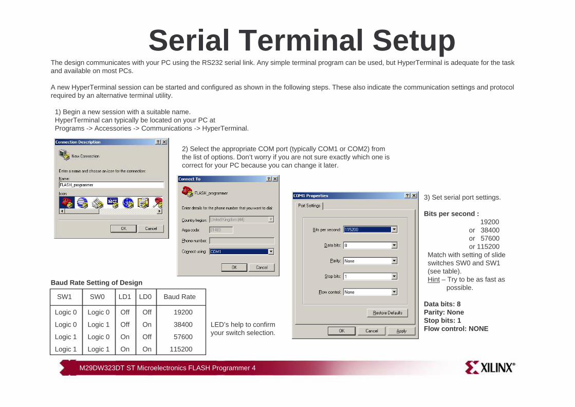
Serial Terminal Setup The design communicates with your PC using the RS232 serial link. Any simple terminal program can be used, but HyperTerminal is adequate for the task and available on most PCs.
A new HyperTerminal session can be started and configured as shown in the following steps. These also indicate the communication settings and protocol required by an alternative terminal utility.
1) Begin a new session with a suitable name.HyperTerminal can typically be located on your PC at Programs -> Accessories -> Communications -> HyperTerminal.
2) Select the appropriate COM port (typically COM1 or COM2) fromthe list of options. Don’t worry if you are not sure exactly which one is correct for your PC because you can change it later.
3) Set serial port settings.
Bits per second :19200
or 38400or 57600or 115200
Match with setting of slideswitches SW0 and SW1(see table).Hint – Try to be as fast as
possible.
Data bits: 8Parity: NoneStop bits: 1Flow control: NONE
SW1 SW0
Logic 0 Logic 0
Logic 0 Logic 1
Logic 1 Logic 0
Logic 1 Logic 1
LD0LD1
Off Off
Off On
On Off
On On
Baud Rate
19200
38400
57600
115200
LED’s help to confirm your switch selection.
Baud Rate Setting of Design
M29DW323DT ST Microelectronics FLASH Programmer 5
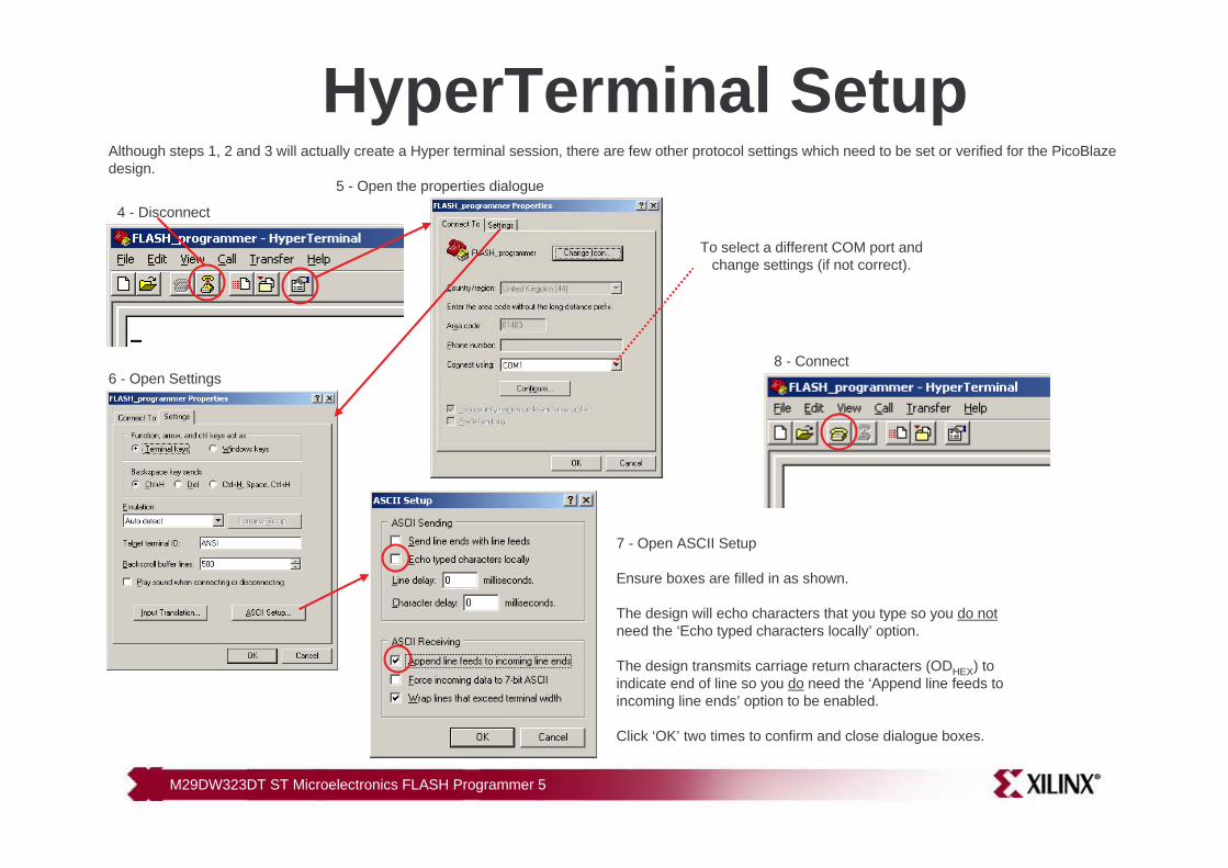
HyperTerminal Setup
4 - Disconnect
5 - Open the properties dialogue
To select a different COM port and change settings (if not correct).
6 - Open Settings
7 - Open ASCII Setup
Ensure boxes are filled in as shown.
The design will echo characters that you type so you do notneed the ‘Echo typed characters locally’ option.
The design transmits carriage return characters (ODHEX) to indicate end of line so you do need the ‘Append line feeds to incoming line ends’ option to be enabled.
Click ‘OK’ two times to confirm and close dialogue boxes.
8 - Connect
Although steps 1, 2 and 3 will actually create a Hyper terminal session, there are few other protocol settings which need to be set or verified for the PicoBlaze design.
M29DW323DT ST Microelectronics FLASH Programmer 6
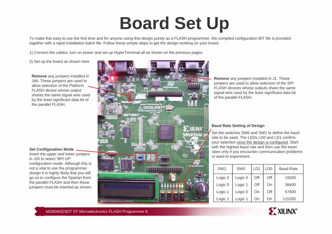
To make this easy to use the first time and for anyone using this design purely as a FLASH programmer, the compiled configuration BIT file is provided together with a rapid installation batch file. Follow these simple steps to get the design working on your board.
Board Set Up 1) Connect the cables, turn on power and set up HyperTerminal all as shown on the previous pages.
2) Set up the board as shown here
Remove any jumpers installed in J1. These jumpers are used to allow selection of the SPI FLASH devices whose outputs share the same signal wire used by the least significant data bit of the parallel FLASH.
SW1 SW0
Logic 0 Logic 0
Logic 0 Logic 1
Logic 1 Logic 0
Logic 1 Logic 1
LD0LD1
Off Off
Off On
On Off
On On
Baud Rate
19200
38400
57600
115200
Baud Rate Setting of Design
Set the switches SW0 and SW1 to define the baud rate to be used. The LEDs LD0 and LD1 confirm your selection once the design is configured. Start with the highest baud rate and then use the lower rates only if you encounter communication problems or want to experiment.
Remove any jumpers installed in J46. These jumpers are used to allow selection of the Platform FLASH device whose output shares the same signal wire used by the least significant data bit of the parallel FLASH.
Set Configuration ModeInsert the upper and lower jumpers in J26 to select ‘BPI UP’configuration mode. Although this is not a vital to use the programmer design it is highly likely that you will go on to configure the Spartan from the parallel FLASH and then these jumpers must be inserted as shown.
M29DW323DT ST Microelectronics FLASH Programmer 7
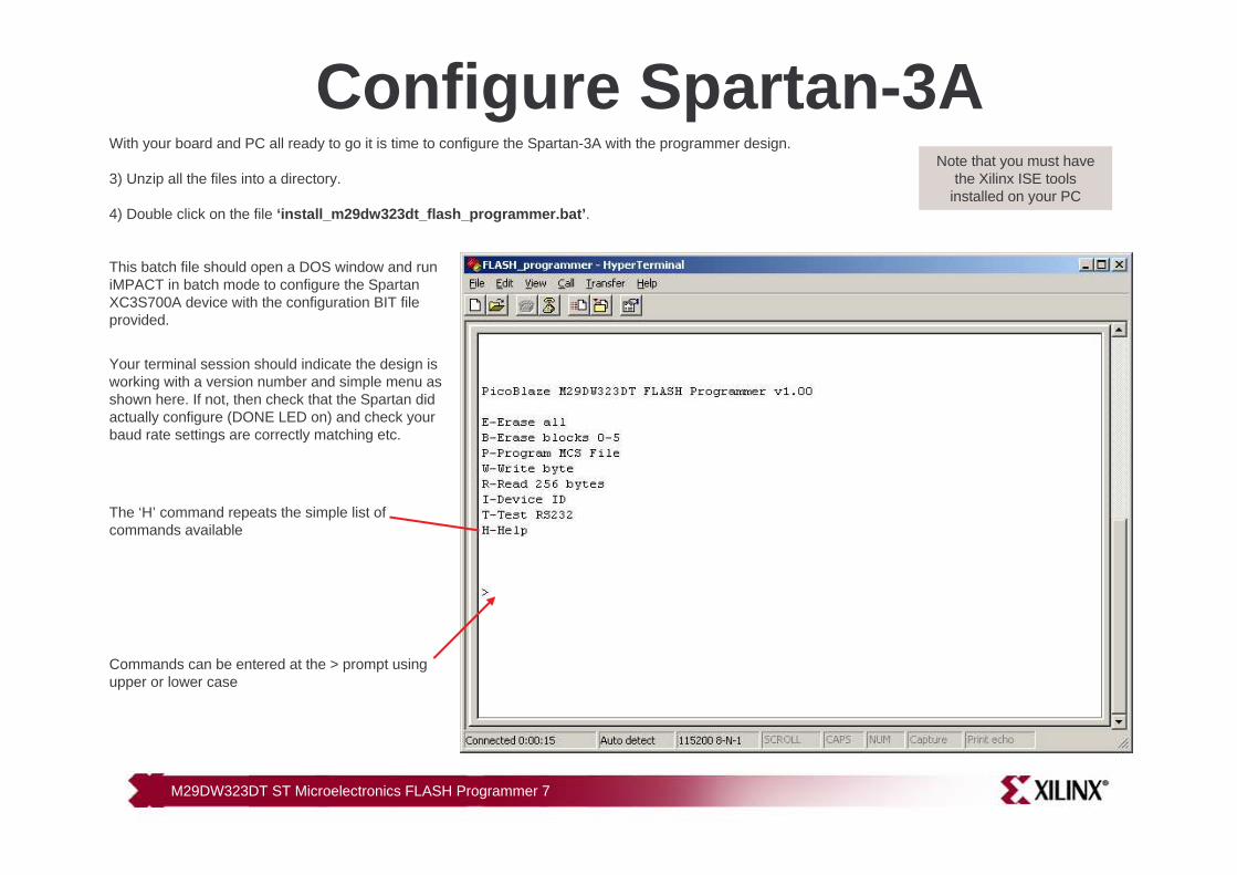
With your board and PC all ready to go it is time to configure the Spartan-3A with the programmer design.
Configure Spartan-3A
Your terminal session should indicate the design is working with a version number and simple menu as shown here. If not, then check that the Spartan did actually configure (DONE LED on) and check your baud rate settings are correctly matching etc.
3) Unzip all the files into a directory.
4) Double click on the file ‘install_m29dw323dt_flash_programmer.bat’.
This batch file should open a DOS window and run iMPACT in batch mode to configure the Spartan XC3S700A device with the configuration BIT file provided.
Note that you must have the Xilinx ISE tools
installed on your PC
The ‘H’ command repeats the simple list of commands available
Commands can be entered at the > prompt using upper or lower case
M29DW323DT ST Microelectronics FLASH Programmer 8
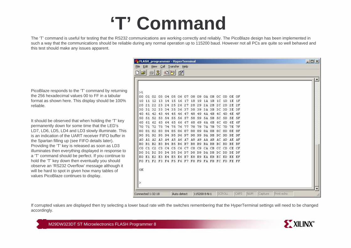
‘T’ Command The ‘T’ command is useful for testing that the RS232 communications are working correctly and reliably. The PicoBlaze design has been implemented in such a way that the communications should be reliable during any normal operation up to 115200 baud. However not all PCs are quite so well behaved and this test should make any issues apparent.
If corrupted values are displayed then try selecting a lower baud rate with the switches remembering that the HyperTerminal settings will need to be changed accordingly.
PicoBlaze responds to the ‘T’ command by returning the 256 hexadecimal values 00 to FF in a tabular format as shown here. This display should be 100% reliable.
It should be observed that when holding the ‘T’ key permanently down for some time that the LED’s LD7, LD6, LD5, LD4 and LD3 slowly illuminate. This is an indication of the UART receiver FIFO buffer in the Spartan filling up (see FIFO details later). Providing the ‘T’ key is released as soon as LD3 illuminates then everything displayed in response to a ‘T’ command should be perfect. If you continue to hold the ‘T’ key down then eventually you should observe an ‘RS232 Overflow’ message although it will be hard to spot in given how many tables of values PicoBlaze continues to display.
M29DW323DT ST Microelectronics FLASH Programmer 9
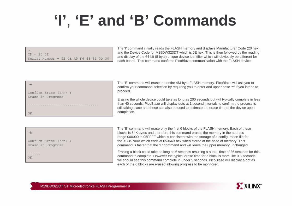
‘I’, ‘E’ and ‘B’ Commands The ‘I’ command initially reads the FLASH memory and displays Manufacturer Code (20 hex) and the Device Code for M29DW323DT which is 5E hex. This is then followed by the reading and display of the 64-bit (8 byte) unique device identifier which will obviously be different for each board. This command confirms PicoBlaze communication with the FLASH device.
The ‘E’ command will erase the entire 4M-byte FLASH memory. PicoBlaze will ask you to confirm your command selection by requiring you to enter and upper case ‘Y’ if you intend to proceed.
>b
Confirm Erase (Y/n) YErase in Progress
......OK
The ‘B’ command will erase only the first 6 blocks of the FLASH memory. Each of these blocks is 64K bytes and therefore this command erases the memory in the address range 000000 to 05FFFF which is consistent with the storage of a configuration file for the XC3S700A which ends at 05364B hex when stored at the base of memory. This command is faster that the ‘E’ command and will leave the upper memory unchanged.
>e
Confirm Erase (Y/n) YErase in Progress
..................................
OK
>iID = 20 5ESerial Number = 52 CE A5 F6 48 31 0D 30
Erasing the whole device could take as long as 200 seconds but will typically complete in less than 40 seconds. PicoBlaze will display dots at 1 second intervals to confirm the process is still taking place and these can also be used to estimate the erase time of the device upon completion.
Erasing a block could take as long as 6 seconds resulting a a total time of 36 seconds for this command to complete. However the typical erase time for a block is more like 0.8 seconds we should see this command complete in under 5 seconds. PicoBlaze will display a dot as each of the 6 blocks are erased allowing progress to be monitored.
M29DW323DT ST Microelectronics FLASH Programmer 10
>w
address = 05ff0adata = 42
OK
>raddress = 05ff00
05FF00 FF FF FF FF FF FF FF FF FF FF 42 FF FF FF FF FF05FF10 FF FF FF FF FF FF FF FF FF FF FF FF FF FF FF FF05FF20 FF FF FF FF FF FF FF FF FF FF FF FF FF FF FF FF05FF30 FF FF FF FF FF FF FF FF FF FF FF FF FF FF FF FF05FF40 FF FF FF FF FF FF FF FF FF FF FF FF FF FF FF FF05FF50 FF FF FF FF FF FF FF FF FF FF FF FF FF FF FF FF05FF60 FF FF FF FF FF FF FF FF FF FF FF FF FF FF FF FF05FF70 FF FF FF FF FF FF FF FF FF FF FF FF FF FF FF FF05FF80 FF FF FF FF FF FF FF FF FF FF FF FF FF FF FF FF05FF90 FF FF FF FF FF FF FF FF FF FF FF FF FF FF FF FF05FFA0 FF FF FF FF FF FF FF FF FF FF FF FF FF FF FF FF05FFB0 FF FF FF FF FF FF FF FF FF FF FF FF FF FF FF FF05FFC0 FF FF FF FF FF FF FF FF FF FF FF FF FF FF FF FF05FFD0 FF FF FF FF FF FF FF FF FF FF FF FF FF FF FF FF05FFE0 FF FF FF FF FF FF FF FF FF FF FF FF FF FF FF FF05FFF0 FF FF FF FF FF FF FF FF FF FF FF FF FF FF FF FF
OK
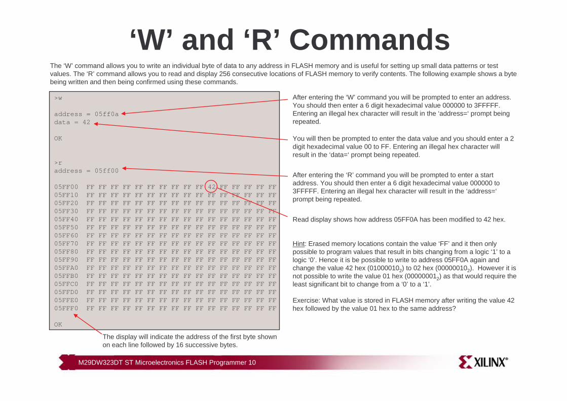
‘W’ and ‘R’ CommandsThe ‘W’ command allows you to write an individual byte of data to any address in FLASH memory and is useful for setting up small data patterns or test values. The ‘R’ command allows you to read and display 256 consecutive locations of FLASH memory to verify contents. The following example shows a byte being written and then being confirmed using these commands.
Read display shows how address 05FF0A has been modified to 42 hex.
After entering the ‘W’ command you will be prompted to enter an address. You should then enter a 6 digit hexadecimal value 000000 to 3FFFFF. Entering an illegal hex character will result in the ‘address=‘ prompt being repeated.
You will then be prompted to enter the data value and you should enter a 2 digit hexadecimal value 00 to FF. Entering an illegal hex character will result in the ‘data=‘ prompt being repeated.
The display will indicate the address of the first byte shown on each line followed by 16 successive bytes.
After entering the ‘R’ command you will be prompted to enter a start address. You should then enter a 6 digit hexadecimal value 000000 to 3FFFFF. Entering an illegal hex character will result in the ‘address=‘prompt being repeated.
Hint: Erased memory locations contain the value ‘FF’ and it then only possible to program values that result in bits changing from a logic ‘1’ to a logic ‘0’. Hence it is be possible to write to address 05FF0A again and change the value 42 hex (010000102) to 02 hex (000000102). However it is not possible to write the value 01 hex (000000012) as that would require the least significant bit to change from a ‘0’ to a ‘1’.
Exercise: What value is stored in FLASH memory after writing the value 42 hex followed by the value 01 hex to the same address?
M29DW323DT ST Microelectronics FLASH Programmer 11
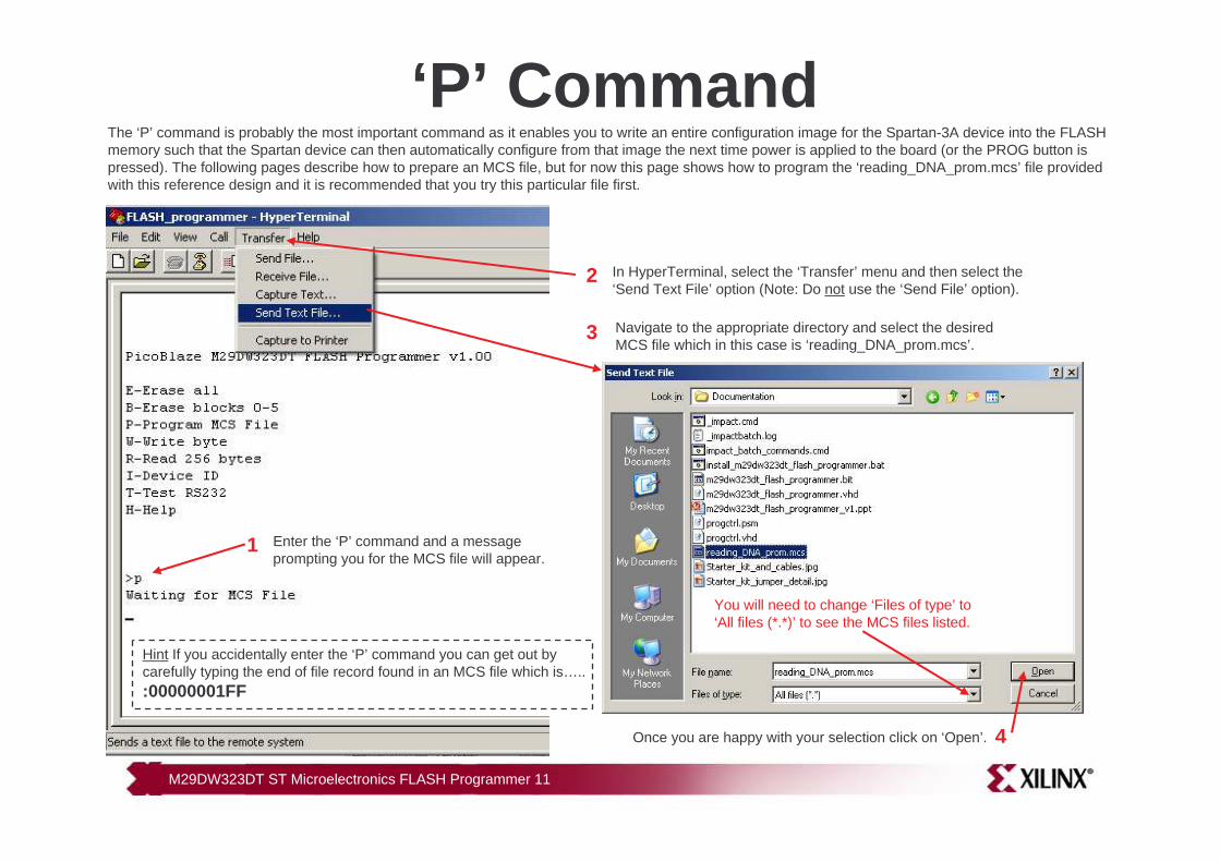
‘P’ Command
Enter the ‘P’ command and a message prompting you for the MCS file will appear.
The ‘P’ command is probably the most important command as it enables you to write an entire configuration image for the Spartan-3A device into the FLASH memory such that the Spartan device can then automatically configure from that image the next time power is applied to the board (or the PROG button is pressed). The following pages describe how to prepare an MCS file, but for now this page shows how to program the ‘reading_DNA_prom.mcs’ file provided with this reference design and it is recommended that you try this particular file first.
In HyperTerminal, select the ‘Transfer’ menu and then select the ‘Send Text File’ option (Note: Do not use the ‘Send File’ option).
Navigate to the appropriate directory and select the desired MCS file which in this case is ‘reading_DNA_prom.mcs’.
Hint If you accidentally enter the ‘P’ command you can get out by carefully typing the end of file record found in an MCS file which is…..:00000001FF
1
2
3
Once you are happy with your selection click on ‘Open’.
You will need to change ‘Files of type’ to ‘All files (*.*)’ to see the MCS files listed.
4
M29DW323DT ST Microelectronics FLASH Programmer 12
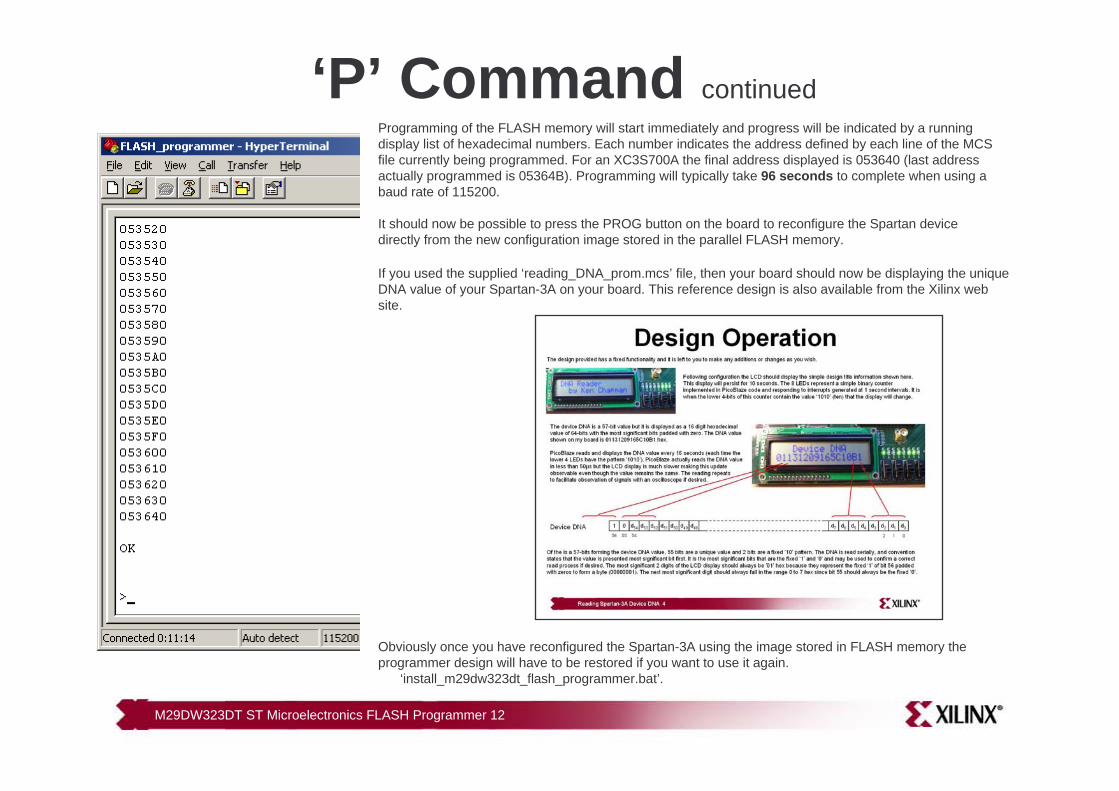
‘P’ Command continuedProgramming of the FLASH memory will start immediately and progress will be indicated by a running display list of hexadecimal numbers. Each number indicates the address defined by each line of the MCS file currently being programmed. For an XC3S700A the final address displayed is 053640 (last address actually programmed is 05364B). Programming will typically take 96 seconds to complete when using a baud rate of 115200.
It should now be possible to press the PROG button on the board to reconfigure the Spartan device directly from the new configuration image stored in the parallel FLASH memory.
Obviously once you have reconfigured the Spartan-3A using the image stored in FLASH memory the programmer design will have to be restored if you want to use it again.
‘install_m29dw323dt_flash_programmer.bat’.
If you used the supplied ‘reading_DNA_prom.mcs’ file, then your board should now be displaying the unique DNA value of your Spartan-3A on your board. This reference design is also available from the Xilinx web site.
M29DW323DT ST Microelectronics FLASH Programmer 13
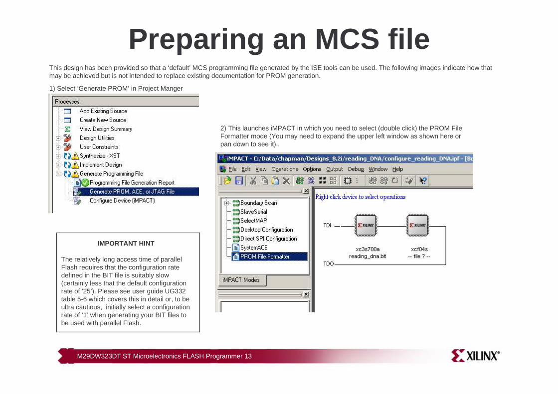
Preparing an MCS fileThis design has been provided so that a ‘default’ MCS programming file generated by the ISE tools can be used. The following images indicate how that may be achieved but is not intended to replace existing documentation for PROM generation.
1) Select ‘Generate PROM’ in Project Manger
2) This launches iMPACT in which you need to select (double click) the PROM File Formatter mode (You may need to expand the upper left window as shown here or pan down to see it)..
IMPORTANT HINT
The relatively long access time of parallel Flash requires that the configuration rate defined in the BIT file is suitably slow (certainly less that the default configuration rate of ’25’). Please see user guide UG332 table 5-6 which covers this in detail or, to be ultra cautious, initially select a configuration rate of ‘1’ when generating your BIT files to be used with parallel Flash.
M29DW323DT ST Microelectronics FLASH Programmer 14
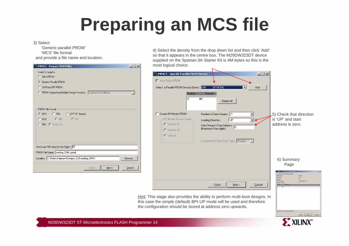
Preparing an MCS file3) Select
‘Generic parallel PROM’‘MCS’ file format
and provide a file name and location.
4) Select the density from the drop down list and then click ‘Add’so that it appears in the centre box. The M29DW323DT device supplied on the Spartan-3A Starter Kit is 4M-bytes so this is the most logical choice.
Hint: This stage also provides the ability to perform multi-boot designs. In this case the simple (default) BPI-UP mode will be used and therefore the configuration should be stored at address zero upwards.
6) Summary Page
5) Check that direction is ‘UP’ and start address is zero.

M29DW323DT ST Microelectronics FLASH Programmer 15
Preparing an MCS file7) You are now presented with a picture of the PROM contents and an ‘Add Device’ box encouraging you to add your first device. Click ‘OK’ to continue.
8) Navigate to the required configuration BIT file, select the file then click ‘Open’.
9) The main window updates to show the BIT file being located at the beginning of the PROM. If you get a the pop up box shown below then you can say ‘No’ for this typical case of a single configuration image.
Hint: If the ‘Add Device’ box does not appear, then right click in the white space and select ‘Add Xilinx Device…’
M29DW323DT ST Microelectronics FLASH Programmer 16
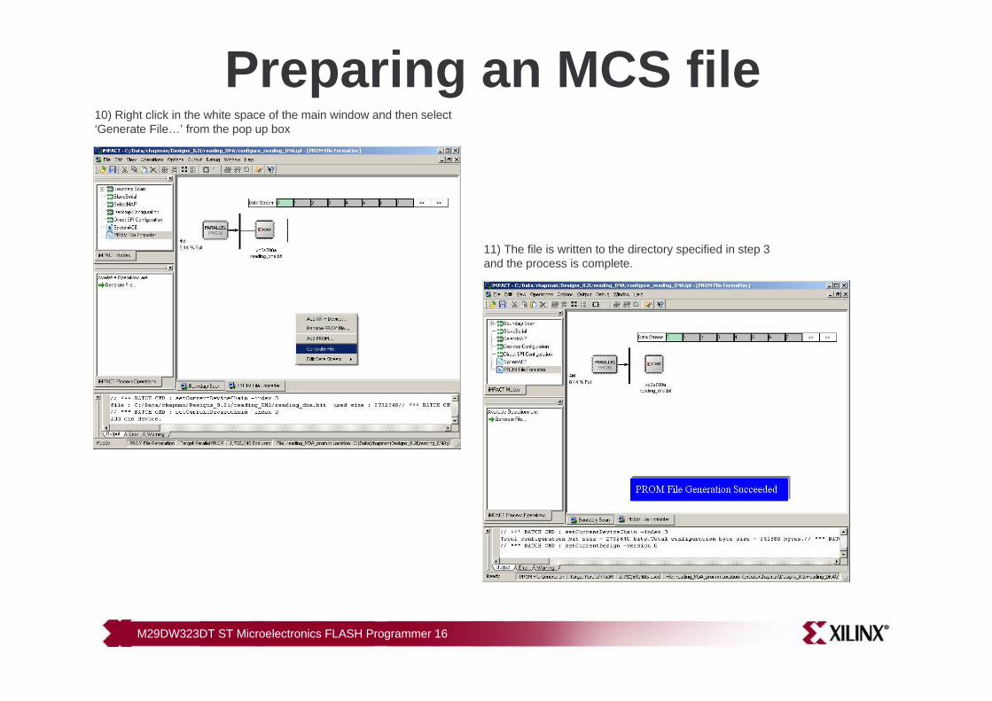
Preparing an MCS file10) Right click in the white space of the main window and then select ‘Generate File…’ from the pop up box
11) The file is written to the directory specified in step 3 and the process is complete.
M29DW323DT ST Microelectronics FLASH Programmer 17
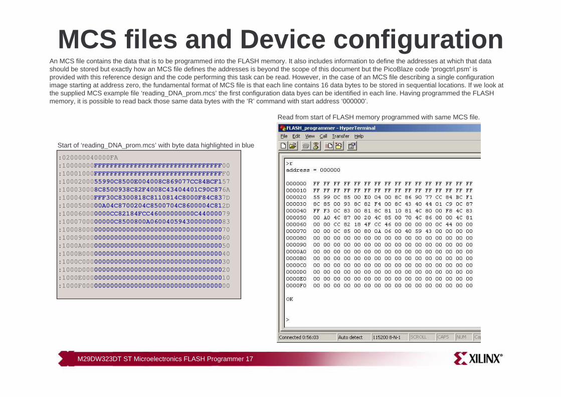
MCS files and Device configuration
:020000040000FA:10000000FFFFFFFFFFFFFFFFFFFFFFFFFFFFFFFF00:10001000FFFFFFFFFFFFFFFFFFFFFFFFFFFFFFFFF0:1000200055990C8500E004008C869077CC84BCF157:100030008C8500938C82F4008C43404401C90C876A:10004000FFF30C8300818C8110814C8000F84C837D:1000500000A04C8700204C8500704C8600004C812D:100060000000CC82184FCC46000000000C44000079:1000700000000C8500800A06004059430000000083:100080000000000000000000000000000000000070:100090000000000000000000000000000000000060:1000A0000000000000000000000000000000000050:1000B0000000000000000000000000000000000040:1000C0000000000000000000000000000000000030:1000D0000000000000000000000000000000000020:1000E0000000000000000000000000000000000010:1000F0000000000000000000000000000000000000
An MCS file contains the data that is to be programmed into the FLASH memory. It also includes information to define the addresses at which that data should be stored but exactly how an MCS file defines the addresses is beyond the scope of this document but the PicoBlaze code ‘progctrl.psm’ is provided with this reference design and the code performing this task can be read. However, in the case of an MCS file describing a single configuration image starting at address zero, the fundamental format of MCS file is that each line contains 16 data bytes to be stored in sequential locations. If we look at the supplied MCS example file ‘reading_DNA_prom.mcs’ the first configuration data byes can be identified in each line. Having programmed the FLASH memory, it is possible to read back those same data bytes with the ‘R’ command with start address ‘000000’.
Start of ‘reading_DNA_prom.mcs’ with byte data highlighted in blue
Read from start of FLASH memory programmed with same MCS file.
M29DW323DT ST Microelectronics FLASH Programmer 18
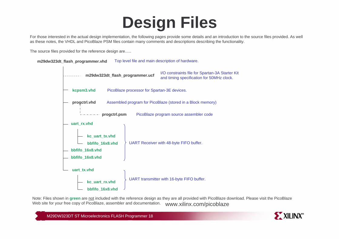
Design FilesFor those interested in the actual design implementation, the following pages provide some details and an introduction to the source files provided. As well as these notes, the VHDL and PicoBlaze PSM files contain many comments and descriptions describing the functionality.
The source files provided for the reference design are…..
m29dw323dt_flash_programmer.vhd
bbfifo_16x8.vhd
kc_uart_tx.vhd
Top level file and main description of hardware.
PicoBlaze program source assembler code
kcpsm3.vhd PicoBlaze processor for Spartan-3E devices.
progctrl.vhd
uart_tx.vhd
bbfifo_16x8.vhd
kc_uart_rx.vhd
UART Receiver with 48-byte FIFO buffer.
m29dw323dt_flash_programmer.ucf I/O constraints file for Spartan-3A Starter Kit and timing specification for 50MHz clock.
progctrl.psm
Assembled program for PicoBlaze (stored in a Block memory)
Note: Files shown in green are not included with the reference design as they are all provided with PicoBlaze download. Please visit the PicoBlaze Web site for your free copy of PicoBlaze, assembler and documentation. www.xilinx.com/picoblaze
uart_rx.vhd
bbfifo_16x8.vhd
bbfifo_16x8.vhd
UART transmitter with 16-byte FIFO buffer.
M29DW323DT ST Microelectronics FLASH Programmer 19
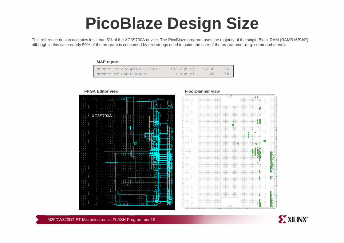
PicoBlaze Design SizeThis reference design occupies less than 5% of the XC3S700A device. The PicoBlaze program uses the majority of the single Block RAM (RAMB16BWE) although in this case nearly 50% of the program is consumed by text strings used to guide the user of the programmer (e.g. command menu).
Number of occupied Slices: 176 out of 5,888 2%Number of RAMB16BWEs: 1 out of 20 5%
MAP report
FPGA Editor view Floorplanner view
XC3S700A
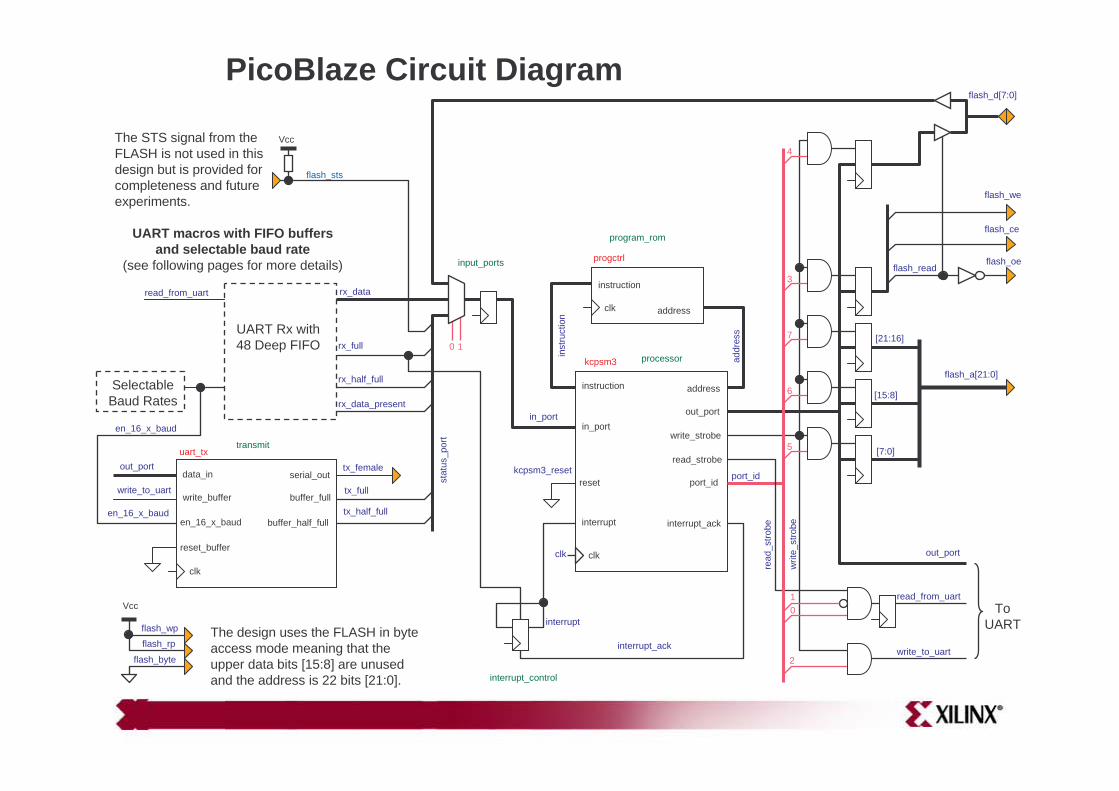
PicoBlaze Circuit Diagram
rx_half_full
rx_full
rx_data_present
read_from_uart rx_data
buffer_full
uart_txtransmit
data_in
clk
serial_out
reset_buffer
en_16_x_baud
write_buffer
buffer_half_fulltx_half_full
tx_full
out_port tx_female
write_to_uart
en_16_x_baud
UART macros with FIFO buffers and selectable baud rate
(see following pages for more details)
flash_byte
stat
us_p
ort
interrupt_control
port_id
kcpsm3 processor
instruction
write_strobe
clk
out_port
read_strobe
address
reset
interrupt_ackinterrupt
in_port
inst
ruct
ion
addr
ess
progctrl
program_rom
instruction
addressclk
port_id
out_port
read
_stro
be
interrupt_ack
interrupt
in_port
clk
kcpsm3_reset
10
read_from_uart
write_to_uart
input_ports
01
2
flash_sts
flash_d[7:0]
Vcc
writ
e_st
robe
4
3
flash_oe
flash_ce
flash_we
flash_read
The design uses the FLASH in byte access mode meaning that the upper data bits [15:8] are unused and the address is 22 bits [21:0].
Vcc
Selectable Baud Rates
UART Rx with 48 Deep FIFO
flash_rp
flash_wp
en_16_x_baud
The STS signal from the FLASH is not used in this design but is provided for completeness and future experiments.
ToUART
5
6
7
[7:0]
[15:8]
[21:16]
flash_a[21:0]
M29DW323DT ST Microelectronics FLASH Programmer 21
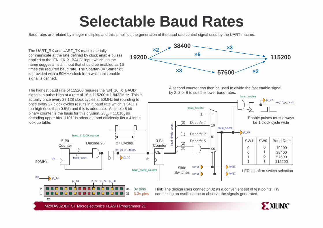
Selectable Baud RatesBaud rates are related by integer multiples and this simplifies the generation of the baud rate control signal used by the UART macros.
19200
57600
38400
115200×2
×2×3
×3
5
baud_count
Decode 26
clk
5-BitCounter
The UART_RX and UART_TX macros serially communicate at the rate defined by clock enable pulses applied to the ‘EN_16_X_BAUD’ input which, as the name suggests, is an input that should be enabled as 16 times the required baud rate. The Spartan-3A Starter kit is provided with a 50MHz clock from which this enable signal is defined.
The highest baud rate of 115200 requires the ‘EN_16_X_BAUD’signals to pulse High at a rate of 16 × 115200 = 1.8432MHz. This is actually once every 27.128 clock cycles at 50MHz but rounding toonce every 27 clock cycles results in a baud rate which is 541Hztoo high (less than 0.5%) and this is adequate. A simple 5 bit binary counter is the basis for this division. 2610 = 110102 so decoding upper bits “1101” is adequate and efficiently fits a 4 input look up table.
50MHz
27 Cycles
×6
A second counter can then be used to divide the fast enable signal by 2, 3 or 6 to suit the lower baud rates.
en_16_x_baud
‘1’
clk
3-BitCounter
CE00
01
10
11
baud_select
SW0SW1
0011
0101
Baud Rate
192003840057600115200
(0)
baud
_div
ide_
coun
t Decode 1Enable pulses must always
be 1 clock cycle wide
en_16_x_115200
(1) Decode 2baud_115200_counter
baud_divide_counter
baud_selector
baud_enable
led(1)
led(0)LEDs confirm switch selection
sw(1)
sw(0)
SlideSwitches
Decode 5(2)(0)
j2_14
j2_26
j2_22
clk
J2
12
3334 0v pins
3.3v pins
j2_30
j2_30j2_26j2_22j2_14
Hint: The design uses connector J2 as a convenient set of test points. Try connecting an oscilloscope to observe the signals generated.
M29DW323DT ST Microelectronics FLASH Programmer 22
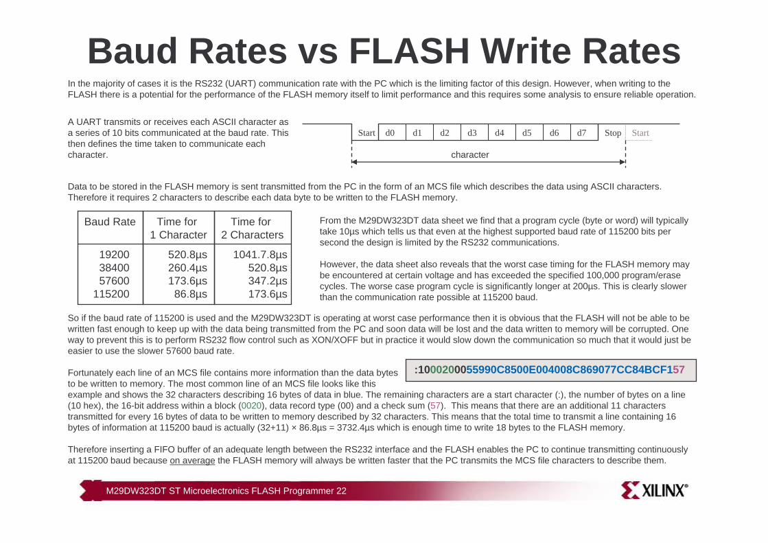
Baud Rates vs FLASH Write RatesIn the majority of cases it is the RS232 (UART) communication rate with the PC which is the limiting factor of this design. However, when writing to the FLASH there is a potential for the performance of the FLASH memory itself to limit performance and this requires some analysis to ensure reliable operation.
Baud Rate
A UART transmits or receives each ASCII character as a series of 10 bits communicated at the baud rate. This then defines the time taken to communicate each character.
d0 d1 d6d2 d3 d4 d5 d7Start Stop Start
character
Data to be stored in the FLASH memory is sent transmitted from the PC in the form of an MCS file which describes the data using ASCII characters. Therefore it requires 2 characters to describe each data byte to be written to the FLASH memory.
Time for 1 Character
Time for 2 Characters
192003840057600
115200
520.8µs260.4µs173.6µs86.8µs
1041.7.8µs520.8µs347.2µs173.6µs
From the M29DW323DT data sheet we find that a program cycle (byte or word) will typically take 10µs which tells us that even at the highest supported baud rate of 115200 bits per second the design is limited by the RS232 communications.
However, the data sheet also reveals that the worst case timing for the FLASH memory may be encountered at certain voltage and has exceeded the specified 100,000 program/erase cycles. The worse case program cycle is significantly longer at 200µs. This is clearly slower than the communication rate possible at 115200 baud.
So if the baud rate of 115200 is used and the M29DW323DT is operating at worst case performance then it is obvious that the FLASH will not be able to be written fast enough to keep up with the data being transmitted from the PC and soon data will be lost and the data written to memory will be corrupted. One way to prevent this is to perform RS232 flow control such as XON/XOFF but in practice it would slow down the communication so much that it would just be easier to use the slower 57600 baud rate.
:1000200055990C8500E004008C869077CC84BCF157Fortunately each line of an MCS file contains more information than the data bytesto be written to memory. The most common line of an MCS file looks like this example and shows the 32 characters describing 16 bytes of data in blue. The remaining characters are a start character (:), the number of bytes on a line (10 hex), the 16-bit address within a block (0020), data record type (00) and a check sum (57). This means that there are an additional 11 characters transmitted for every 16 bytes of data to be written to memory described by 32 characters. This means that the total time to transmit a line containing 16 bytes of information at 115200 baud is actually (32+11) × 86.8µs = 3732.4µs which is enough time to write 18 bytes to the FLASH memory.
Therefore inserting a FIFO buffer of an adequate length between the RS232 interface and the FLASH enables the PC to continue transmitting continuously at 115200 baud because on average the FLASH memory will always be written faster that the PC transmits the MCS file characters to describe them.
M29DW323DT ST Microelectronics FLASH Programmer 23
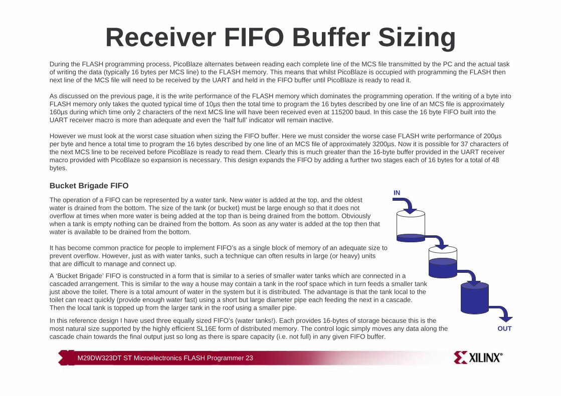
Receiver FIFO Buffer SizingDuring the FLASH programming process, PicoBlaze alternates between reading each complete line of the MCS file transmitted by the PC and the actual task of writing the data (typically 16 bytes per MCS line) to the FLASH memory. This means that whilst PicoBlaze is occupied with programming the FLASH then next line of the MCS file will need to be received by the UART and held in the FIFO buffer until PicoBlaze is ready to read it.
As discussed on the previous page, it is the write performance of the FLASH memory which dominates the programming operation. If the writing of a byte into FLASH memory only takes the quoted typical time of 10µs then the total time to program the 16 bytes described by one line of an MCS file is approximately 160µs during which time only 2 characters of the next MCS line will have been received even at 115200 baud. In this case the 16 byte FIFO built into the UART receiver macro is more than adequate and even the ‘half full’ indicator will remain inactive.
However we must look at the worst case situation when sizing the FIFO buffer. Here we must consider the worse case FLASH write performance of 200µs per byte and hence a total time to program the 16 bytes described by one line of an MCS file of approximately 3200µs. Now it is possible for 37 characters of the next MCS line to be received before PicoBlaze is ready to read them. Clearly this is much greater than the 16-byte buffer provided in the UART receiver macro provided with PicoBlaze so expansion is necessary. This design expands the FIFO by adding a further two stages each of 16 bytes for a total of 48 bytes.
Bucket Brigade FIFO
The operation of a FIFO can be represented by a water tank. New water is added at the top, and the oldest water is drained from the bottom. The size of the tank (or bucket) must be large enough so that it does not overflow at times when more water is being added at the top than is being drained from the bottom. Obviously when a tank is empty nothing can be drained from the bottom. As soon as any water is added at the top then that water is available to be drained from the bottom.
IN
OUT
It has become common practice for people to implement FIFO’s as a single block of memory of an adequate size to prevent overflow. However, just as with water tanks, such a technique can often results in large (or heavy) units that are difficult to manage and connect up.
A ‘Bucket Brigade’ FIFO is constructed in a form that is similar to a series of smaller water tanks which are connected in a cascaded arrangement. This is similar to the way a house may contain a tank in the roof space which in turn feeds a smaller tankjust above the toilet. There is a total amount of water in the system but it is distributed. The advantage is that the tank local to the toilet can react quickly (provide enough water fast) using a short but large diameter pipe each feeding the next in a cascade. Then the local tank is topped up from the larger tank in the roof using a smaller pipe.
In this reference design I have used three equally sized FIFO’s (water tanks!). Each provides 16-bytes of storage because this is the most natural size supported by the highly efficient SL16E form of distributed memory. The control logic simply moves any data along the cascade chain towards the final output just so long as there is spare capacity (i.e. not full) in any given FIFO buffer.
M29DW323DT ST Microelectronics FLASH Programmer 24
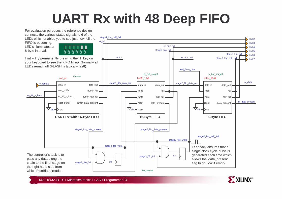
For evaluation purposes the reference design connects the various status signals to 6 of the LEDs which enables you to see just how full the FIFO is becoming. LED’s illuminates at8-byte intervals.
UART Rx with 48 Deep FIFO
buffer_full
uart_rxreceive
serial_in
clk
data_out
reset_buffer buffer_data_present
en_16_x_baud
read_buffer
buffer_half_full
rx_full
rx_data_present
rx_female
full
bbfifo_16x8
rx_buf_stage2
data_out
read
half_full
data_in
write
clk clk
reset
clk
stage1_fifo_data_out
en_16_x_baud
stage2_fifo_data_present
stage1_fifo_half_full
stage2_fifo_half_full
stage2_fifo_data_out
data_present
full
bbfifo_16x8
rx_buf_stage3
data_out
read
half_full
read_from_uart
data_in
write
clk
reset
clk
rx_data
data_present
stage3_fifo_half_full
stage3_fifo_full
clk
stage3_fifo_write
led(5)
led(6)
led(7)
led(2)
led(3)
led(4)
stage3_fifo_full
Feedback ensures that a single clock cycle pulse is generated each time which allows the ‘data_present’flag to go Low if empty.clk
stage2_fifo_write
stage2_fifo_full
stage1_fifo_data_present
stage2_fifo_full
rx_half_full
rx_half_fullrx_full
UART Rx with 16-Byte FIFO 16-Byte FIFO 16-Byte FIFO
The controller’s task is to pass any data along the chain to the final stage on the right hand side from which PicoBlaze reads. fifo_control
LD7
LD6
LD5
LD4
LD3
LD2
Hint – Try permanently pressing the ‘T’ key on your keyboard to see the FIFO fill up. Normally all LEDs remain off (FLASH is typically fast!)
M29DW323DT ST Microelectronics FLASH Programmer 25
Reading FLASH MemoryReading the parallel FLASH memory is relatively straightforward. The only issue for PicoBlaze is that it does not have a 24-bit address range and therefore multiple ports are used to achieve the operation.
Set 24-bit address form which to read
Set controls for read
Deselect FLASH memory
Read data after a delay of >70ns
Bit 0 - flash_read=‘1’Enables memory outputs (flash_oe=‘0’)Tri-states the Spartan outputs (flash_d=‘Z’)
Bit 1 - flash_ce=‘0’Enables memory
Bit 2 - flash_we=‘1’Write enable is off (read operation)
50MHz clock
flash_a
LOA
D
OU
TPU
T
OU
TPU
T
LOA
D
LOA
D
INP
UT
OU
TPU
T
RE
TUR
N
OU
TPU
T
OU
TPU
T
Actual read point of FLASH
All PicoBlaze instructions execute in 2 clock cycles and the design uses the 50MHz clock source on the board. Therefore all instructions take 40ns to execute and this makes all timing of the design easy to predict and ensures that the specifications of the FLASH memory are met.
flash_oe
flash_ce
flash_we
flash_d Spartan driving
100ns
The access time of the memory is 70ns (see ST Microelectronics data sheet for details). By including an additional LOAD instruction, the time between setting the controls to read the memory and the actual point of reading is increased by 40ns to allow for this worse case response time.
FLASH_byte_read: OUTPUT s9, FLASH_addr_hi_portOUTPUT s8, FLASH_addr_mi_portOUTPUT s7, FLASH_addr_lo_portLOAD s1, 05OUTPUT s1, FLASH_control_portLOAD s1, 06LOAD s1, 06INPUT s0, FLASH_data_in_portOUTPUT s1, FLASH_control_portRETURN
Note that the input port multiplexer is pipelined which means that the data from the memory is captured on the first clock edge of the INPUTinstruction (as indicated) and then passed into the ‘s0’ register within PicoBlaze on the second clock edge.
PicoBlaze reads FLASH data value captured by input multiplexer
Hint: PicoBlaze code supplied has full comments
M29DW323DT ST Microelectronics FLASH Programmer 26
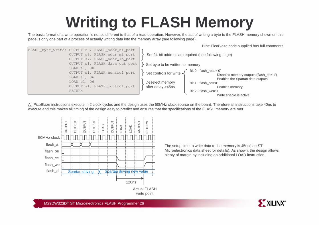
Writing to FLASH MemoryThe basic format of a write operation is not so different to that of a read operation. However, the act of writing a byte to the FLASH memory shown on this page is only one part of a process of actually writing data into the memory array (see following page).
FLASH_byte_write: OUTPUT s9, FLASH_addr_hi_portOUTPUT s8, FLASH_addr_mi_portOUTPUT s7, FLASH_addr_lo_portOUTPUT s1, FLASH_data_out_portLOAD s1, 00OUTPUT s1, FLASH_control_portLOAD s1, 06LOAD s1, 06OUTPUT s1, FLASH_control_portRETURN
Set 24-bit address as required (see following page)
Set controls for write
Deselect memory after delay >45ns
Bit 0 - flash_read=‘0’Disables memory outputs (flash_oe=‘1’)Enables the Spartan data outputs
Bit 1 - flash_ce=‘0’Enables memory
Bit 2 - flash_we=‘0’Write enable is active
50MHz clock
flash_a
LOA
D
OU
TPU
T
OU
TPU
T
LOA
D
LOA
D
OU
TPU
T
RE
TUR
N
OU
TPU
T
OU
TPU
T
Actual FLASH write point
flash_oe
flash_ce
flash_we
flash_d Spartan driving
120ns
The setup time to write data to the memory is 45ns(see ST Microelectronics data sheet for details). As shown, the design allows plenty of margin by including an additional LOAD instruction.
Set byte to be written to memory
OU
TPU
T
Hint: PicoBlaze code supplied has full comments
All PicoBlaze instructions execute in 2 clock cycles and the design uses the 50MHz clock source on the board. Therefore all instructions take 40ns to execute and this makes all timing of the design easy to predict and ensures that the specifications of the FLASH memory are met.
Spartan driving new value
M29DW323DT ST Microelectronics FLASH Programmer 27
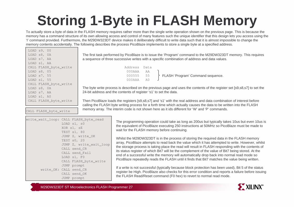
Storing 1-Byte in FLASH MemoryTo actually store a byte of data in the FLASH memory requires rather more than the single write operation shown on the previous page. This is because the memory has a command structure of its own allowing access and control of many features such the unique identifier that this design lets you access using the ‘I’ command provided. Furthermore, the M29DW323DT device makes it deliberately difficult to write data such that it is almost impossible to change the memory contents accidentally. The following describes the process PicoBlaze implements to store a single byte at a specified address.
LOAD s9, 00LOAD s8, 0ALOAD s7, AALOAD s1, AACALL FLASH_byte_writeLOAD s8, 05LOAD s7, 55LOAD s1, 55CALL FLASH_byte_writeLOAD s8, 0ALOAD s7, AALOAD s1, A0CALL FLASH_byte_write Then PicoBlaze loads the registers [s9,s8,s7] and ‘s1’ with the real address and data combination of interest before
calling the FLASH byte writing process for a forth time which actually causes the data to be written into the FLASH memory array. The interim code is not shown here as it ids different for ‘W’ and ‘P’ commands.
The first task performed by PicoBlaze is to issue the ‘Program’ command to the M29DW323DT memory. This requires a sequence of three successive writes with a specific combination of address and data values.
CALL FLASH_byte_write
The programming operation could take as long as 200us but typically takes 10us but even 10us is the equivalent of PicoBlaze executing 250 instructions at 50MHz so PicoBlaze must be made to wait for the FLASH memory before continuing.
Whilst the M29DW323DT is in the process of storing the required data in the FLASH memory array, PicoBlaze attempts to read back the value which it has attempted to write. However, whilst the storage process is taking place the read will result in FLASH responding with the contents of its status register of which Bit7 will be the complement of the value of Bit7 being stored. At the end of a successful write the memory will automatically drop back into normal read mode so PicoBlaze repeatedly reads the FLASH until it finds that Bit7 matches the value being written.
If a write is not successful (typically because block protection has been used), Bit 5 of the status register be High. PicoBlaze also checks for this error condition and reports a failure before issuing the FLASH Read/Reset command (F0 hex) to revert to normal read mode.
Address Data000AAA AA000555 55000AAA A0
FLASH ‘Program’ Command sequence.
The byte write process is described on the previous page and uses the contents of the register set [s9,s8,s7] to set the 24-bit address and the contents of register ‘s1’ to set the data.
write_wait_loop: CALL FLASH_byte_readLOAD s1, s0XOR s1, sETEST s1, 80JUMP Z, write_OKTEST s0, 20JUMP Z, write_wait_loopCALL send_CRCALL send_FailLOAD s1, F0CALL FLASH_byte_writeJUMP prompt
write_OK: CALL send_CRCALL send_OKJUMP prompt