
LWRpro: An Energy-9fficient Configurable Crypto-Processor ...
14
1 LWRpro: An Energy-∃fficient Configurable Crypto-Processor for Module-LWR Yihong Zhu, Min Zhu, Bohan Yang, Wenping Zhu, Chenchen Deng, Chen Chen, Shaojun Wei, Leibo Liu. Abstract—Saber, the only module-learning with rounding- based algorithm in NIST’s third round of post-quantum cryptog- raphy (PQC) standardization process, is characterized by sim- plicity and flexibility. However, energy-efficient implementation of Saber is still under investigation since the commonly used number theoretic transform can not be utilized directly. In this manuscript, an energy-efficient configurable crypto-processor supporting multi-security-level key encapsulation mechanism of Saber, is proposed. First, an 8-level hierarchical Karatsuba framework is utilized to reduce degree-256 polynomial multipli- cation to the coefficient-wise multiplication. Second, a hardware- efficient Karatsuba scheduling strategy and an optimized pre- /post-processing structure is designed to reduce the area over- heads of scheduling strategy. Third, a task-rescheduling-based pipeline strategy and truncated multipliers are proposed to enable fine-grained processing. Moreover, multiple parameter sets are supported in LWRpro to enable configurability among vari- ous security scenarios. Enabled by these optimizations, LWRpro requires 1066, 1456 and 1701 clock cycles for key generation, encapsulation, and decapsulation of Saber768. The post-layout version of LWRpro is implemented with TSMC 40 nm CMOS process within 0.38 mm 2 . The throughput for Saber768 is up to 275k encapsulation operations per second and the energy efficiency is 0.15 uJ/encapsulation while operating at 400 MHz, achieving nearly 50× improvement and 31× improvement, re- spectively compared with current PQC hardware solutions. Index Terms—Module-LWR, Saber, crypto-processor, energy- efficient, Karatsuba, hierarchical calculation framework. I. I NTRODUCTION S ABER, a lattice-based public key cryptography scheme, is one of the finalists in the third round competition of National Institute of Standards and Technology (NIST). The main computational bottleneck of Saber is polynomial multiplication, which can not be accelerated by number theo- retic transform (NTT) fast multiplication algorithm. Saber is also characterized by its direct error introducing technique of rounding without specific modular operations. For hardware implementation, how to efficiently implement polynomial mul- tiplication without using NTT-style calculation is an important topic. As the only module-learning with rounding (LWR)-based candidate, Saber has been optimized on the Intel Xeon pro- cessors [1], [2], ARM Cortex-series [3] and FPGA platforms [4]–[6]. For software implementations, a hybrid method com- bining Toom-Cook and Karatsuba algorithm is utilized for efficient implementations of polynomial multiplications [1]– [3]. For hardware implementations, the simple but efficient This work was supported in part by the National Natural Science Foundation of China under Grant 61672317 and Grant 61804088. (Corresponding author: Leibo Liu.) schoolbook multiplication is utilized in [4], [5]. A 4-way Toom-Cook method is utilized to reduce 43% of the number of multiplication operations [6]. However, the efficiency of hardware implementation of fast multiplication algorithm of Saber can be further optimized. An energy-efficient configurable crypto-processor, LWRpro, is proposed based on the algorithm-hardware co-design of module-LWR with multiple security levels of key encapsu- latiom mechanism (KEM). The main computation block of LWRpro is an 8-level recursive split hierarchical Karatsuba framework, which reduces the degree-256 polynomial multi- plication to the coefficient-wise multiplication. Several opti- mization strategies, including optimized pre-/post-processing structure, the task-rescheduling-based pipeline and truncated multiplier, are developed to further improve the energy effi- ciency of LWRpro. In order to make a comprehensive assess- ment of the proposed methods, LWRpro has been implemented on Xilinx Virtex UltraScale+ FPGA platform for PKE version and post-layout ASIC implementation on TSMC 40nm process for KEM version. Compared with the state-of-the-art FPGA implementation of Saber [5], nearly 3.6× reduction in cycles of polynomial multiplications is achieved. The post-layout implementation results show that the speed of LWRpro is 51× and 50× faster than the state-of-the-art implementation of Newhope1024 and Kyber1024 [7]. The energy efficiency of LWRpro is 29× and 33× higher and area efficiency (estimated by the reciprocal of equivalent gates-time product) is 112× and 109× higher, respectively. The key contributions of this work are summarized as follows: 1) Hierarchical Karatsuba framework is utilized to acceler- ate the degree-256 polynomial multiplication in Saber. 2) Sequential hardware-efficient Karatsuba scheduling for post-processing and compact input pre-processing are proposed for the hierarchical Karatsuba framework. 3) Task-rescheduling based pipelining strategy and trun- cated multipliers empower LWRpro to achieve lower latency with a small area. 4) Multi-parameter components and core modules reusage enable LWRpro configurability among three security levels to meet different security scenarios. Compared with the schoolbook multiplication, more than 90% of multiplication operations are saved through 8-level hierarchical Karatsuba framework. Optimization strategies of hierarchical Karatsuba framework, including post-processing and pre-processing circuits, reduce 90.5% of registers and 96.0% of adders compared with the existing partial-reusage solutions. From an implementation aspect, pipelining strat-
Transcript of LWRpro: An Energy-9fficient Configurable Crypto-Processor ...

1
LWRpro: An Energy-∃fficient ConfigurableCrypto-Processor for Module-LWR
Yihong Zhu, Min Zhu, Bohan Yang, Wenping Zhu, Chenchen Deng, Chen Chen, Shaojun Wei, Leibo Liu.
Abstract—Saber, the only module-learning with rounding-based algorithm in NIST’s third round of post-quantum cryptog-raphy (PQC) standardization process, is characterized by sim-plicity and flexibility. However, energy-efficient implementationof Saber is still under investigation since the commonly usednumber theoretic transform can not be utilized directly. In thismanuscript, an energy-efficient configurable crypto-processorsupporting multi-security-level key encapsulation mechanism ofSaber, is proposed. First, an 8-level hierarchical Karatsubaframework is utilized to reduce degree-256 polynomial multipli-cation to the coefficient-wise multiplication. Second, a hardware-efficient Karatsuba scheduling strategy and an optimized pre-/post-processing structure is designed to reduce the area over-heads of scheduling strategy. Third, a task-rescheduling-basedpipeline strategy and truncated multipliers are proposed toenable fine-grained processing. Moreover, multiple parameter setsare supported in LWRpro to enable configurability among vari-ous security scenarios. Enabled by these optimizations, LWRprorequires 1066, 1456 and 1701 clock cycles for key generation,encapsulation, and decapsulation of Saber768. The post-layoutversion of LWRpro is implemented with TSMC 40 nm CMOSprocess within 0.38 mm2. The throughput for Saber768 is upto 275k encapsulation operations per second and the energyefficiency is 0.15 uJ/encapsulation while operating at 400 MHz,achieving nearly 50× improvement and 31× improvement, re-spectively compared with current PQC hardware solutions.
Index Terms—Module-LWR, Saber, crypto-processor, energy-efficient, Karatsuba, hierarchical calculation framework.
I. INTRODUCTION
SABER, a lattice-based public key cryptography scheme,is one of the finalists in the third round competition
of National Institute of Standards and Technology (NIST).The main computational bottleneck of Saber is polynomialmultiplication, which can not be accelerated by number theo-retic transform (NTT) fast multiplication algorithm. Saber isalso characterized by its direct error introducing technique ofrounding without specific modular operations. For hardwareimplementation, how to efficiently implement polynomial mul-tiplication without using NTT-style calculation is an importanttopic.
As the only module-learning with rounding (LWR)-basedcandidate, Saber has been optimized on the Intel Xeon pro-cessors [1], [2], ARM Cortex-series [3] and FPGA platforms[4]–[6]. For software implementations, a hybrid method com-bining Toom-Cook and Karatsuba algorithm is utilized forefficient implementations of polynomial multiplications [1]–[3]. For hardware implementations, the simple but efficient
This work was supported in part by the National Natural Science Foundationof China under Grant 61672317 and Grant 61804088. (Corresponding author:Leibo Liu.)
schoolbook multiplication is utilized in [4], [5]. A 4-wayToom-Cook method is utilized to reduce 43% of the numberof multiplication operations [6]. However, the efficiency ofhardware implementation of fast multiplication algorithm ofSaber can be further optimized.
An energy-efficient configurable crypto-processor, LWRpro,is proposed based on the algorithm-hardware co-design ofmodule-LWR with multiple security levels of key encapsu-latiom mechanism (KEM). The main computation block ofLWRpro is an 8-level recursive split hierarchical Karatsubaframework, which reduces the degree-256 polynomial multi-plication to the coefficient-wise multiplication. Several opti-mization strategies, including optimized pre-/post-processingstructure, the task-rescheduling-based pipeline and truncatedmultiplier, are developed to further improve the energy effi-ciency of LWRpro. In order to make a comprehensive assess-ment of the proposed methods, LWRpro has been implementedon Xilinx Virtex UltraScale+ FPGA platform for PKE versionand post-layout ASIC implementation on TSMC 40nm processfor KEM version. Compared with the state-of-the-art FPGAimplementation of Saber [5], nearly 3.6× reduction in cyclesof polynomial multiplications is achieved. The post-layoutimplementation results show that the speed of LWRpro is51× and 50× faster than the state-of-the-art implementationof Newhope1024 and Kyber1024 [7]. The energy efficiency ofLWRpro is 29× and 33× higher and area efficiency (estimatedby the reciprocal of equivalent gates-time product) is 112× and109× higher, respectively. The key contributions of this workare summarized as follows:
1) Hierarchical Karatsuba framework is utilized to acceler-ate the degree-256 polynomial multiplication in Saber.
2) Sequential hardware-efficient Karatsuba scheduling forpost-processing and compact input pre-processing areproposed for the hierarchical Karatsuba framework.
3) Task-rescheduling based pipelining strategy and trun-cated multipliers empower LWRpro to achieve lowerlatency with a small area.
4) Multi-parameter components and core modules reusageenable LWRpro configurability among three securitylevels to meet different security scenarios.
Compared with the schoolbook multiplication, more than90% of multiplication operations are saved through 8-levelhierarchical Karatsuba framework. Optimization strategies ofhierarchical Karatsuba framework, including post-processingand pre-processing circuits, reduce 90.5% of registers and96.0% of adders compared with the existing partial-reusagesolutions. From an implementation aspect, pipelining strat-
2
egy and truncated multipliers empower LWRpro to achievea speed-up of nearly 50× with 45.6% less resource usagecompared with [7].
The remaining part of this paper is organized as fol-lows. Section II introduces the background of Saber andthe motivations to design LWRpro. Section III proposes theoptimized hierarchical Karatsuba framework with optimizedpre-processing and post-processing structure. In Section IV,the hardware architectures of LWRpro and details of thecustomized circuits are presented. Section V presents theperformance of LWRpro and comparisons with other hardwareimplementations. Finally, this paper is concluded in SectionVI.
II. BACKGROUND AND MOTIVATION
A. Module-LWR and Saber
The LWR scheme, first described in [8], is regarded asa derandomized version of the learning with errors (LWE)scheme. The unique property of LWR scheme lies in thatthe coefficients of polynomials belong to Z2n and it in-troduces randomness through rounding operation. From animplementation aspect, rounding in LWR implies that modularoperations are realized by a simple shifting operation withnegligible costs. NTT can not be used in LWR scheme becausecoefficients of polynomials belong to Z2n rather than a primefield.
The three stages of public key encryption (PKE) scheme ofSaber [1] are shown in Algo. 1, 2 and 3, where l=2/3/4 andεt =3/4/6 are for LightSaber, Saber768 and FireSaber, respec-tively. The Saber-suite offers three security levels: LightSaber,Saber and FireSaber. To avoid confusion, the general term forSaber-suite is referred as Saber in this paper, and Saber768denotes the intermediate security level. Function U denotes theuniform distribution and the function βµ denotes the binomialsampling operation with the corresponding standard deviationσ =
√µ/2. The function bits(v, ε1, ε2) denotes the bits
truncation function in which the bits of v from ε1− ε2+1)-thbit to ε1-th bit are remained.
Algorithm 1 Saber Key Generation
seedA ← U({0, 1}256)A ← gen(seedA) ∈ Rql×ls ← βµ (Rq
l×1)b = bits(AT s, εq , εp) ∈ Rpl×1return (pk = (b, seedA), sk = s )
Algorithm 2 Saber EncryptionInput: seedA, mA ← gen(seedA) ∈ Rql×ls′ ← βµ (Rq
l×1)b′ = bits(As′, εq , εp) ∈ Rpl×1v′ = bT bits(s′, εp, εp)+h1 ∈ Rpcm = bits(v′+2εp−1m, εp, εt + 1) ∈ R2t
return c = (cm, b′)
Algorithm 3 Saber DecryptionInput: s, b′ cmv = b′
T bits(s, εp, εp)+h1 ∈ Rpm′ = bits(v − 2εp−εt−1cm + h2, εp, 1) ∈ R2
return m′
Pesudo-random numbers in public matrix of polynomials Aare generated from the Keccak. Secret vector of polynomialss is generated from binomial sampling. The main computa-tional tasks among all stages are matrix-vector polynomialmultiplications and vector-vector polynomial multiplicationsin Zq[X]/(xn + 1). Matrix-vector polynomial multiplicationsare categorized in two kinds according to the generation orderof public matrix: column-major order during key generationand row-major order during encryption. Some parameters aredifferent among three security levels: the number of polyno-mial multiplications, the number of effective bits of secret keyand number of output bits in encryption.
Two additional hash functions, namely, SHA3-256 andSHA3-512, are needed to support KEM based on PKE scheme.Keccak is the core module of these hash operations. Besides,there is an additional verification operation during decapsula-tion to check whether the ciphertext is qualified or not.
B. Karatsuba Algorithm
The unique property of Saber makes NTT inappropriate forefficient computations. General options, such as Toom-Cookand Karatsuba algorithms, seem to be suitable for efficientpolynomial multiplication in Saber. However, the high-speedimplementation of Toom-Cook incurs additional overheadsresulting from multiple instantiations of evaluation and in-terpolation components [9]. Therefore, Karatsuba algorithmis adopted in LWRpro benefiting from its good scalabil-ity in hardware. The Karatsuba algorithm, firstly proposedin [10], reduces the computational complexity from O(n2) toO(nlog2
3
). Taking the calculation P =M×N as an example,M and N are both n-bit wide, and ML/MH and NL/NHdenote the lower/higher halves of M and N , respectively.As shown in Eq. (1), Karatsuba algorithm can reduce n-bitmultiplication to three n/2-bit multiplication operations andfour n-bit addition operations, where θ, τ and γ denote threeimmediate multiplication results. Eq. (1) only illustrates 1-level Karatsuba algorithm and multi-level Karatsuba algorithmis feasible when ML/MH and NL/NH are split recursivelyfollowing the same rule.
θ =ML ×NL,τ =MH ×NH ,γ = (ML +MH)× (NL +NH),
P =M ×N = θ + (γ − θ − τ)× 2n2 + τ × 2n.
(1)
The number of addition operations is further reducedin [11]. The idea is to avoid the accumulation of overlappingparts, and thus, only seven n/2-bit addition operations arerequired. This is also adopted in the design of LWRpro.
3
C. Related works and Motivation
There are a few works on LWE and ring-LWE schemeson FPGAs [6], [12]–[15] and ASIC platforms [4], [16]–[22].These implementations are based on NTT-style calculationmechanisms and these works are not applicable to Saber.
Existing implementations in [4], [5] utilized the straight-forward schoolbook method without reducing the number ofmultiplication operations. The work [6] utilizing 4-way Toom-Cook algorithm is slower than those based on schoolbookmethods. Moreover, only [5] implemented unified Saber ofmulti-security levels and other works only focused one ver-sion of Saber. How to maximize the advantages broughtby efficient multiplication algorithms, such as Karatsuba orToom-Cook algorithm, for Saber in hardware and how tosupport configurable design for module-LWR still requiresfurther discussion. Hierarchical Karatsuba framework is firstlyutilized in this paper to accelerate polynomial multiplication.Correspondingly, the overhead and hardware are discussed.
Karatsuba-based systolic multipliers are usually used toaccelerate large-number multiplication in hardware implemen-tations of ECC and RSA algorithms [23]–[26]. Unfortunately,utilizing Karatsuba-based systolic multipliers for Saber re-sults in large area cost, which means that the traditionalmethod cannot be directly applied to Saber. A hierarchicalKaratsuba implementation is proposed in [27] by employingthe 64-bit conventional Karatsuba multiplier as the kernelhardware to implement RSA-type algorithm. Therefore, a 256-bit multiplication is accomplished by executing this kernel9 times through Karatsuba scheduling strategy. Although thecomputational tasks are fully covered by reusing the relativelysmall Karatsuba multipliers, numerous registers and adders inthe scheduling layer are required to keep all the intermediatedata. This overhead also becomes high if the computationaltasks are large. Several optimized strategies are proposed inthe design of LWRpro to reduce this overhead of implementingSaber. Modules in pre-processing circuits are reused and alloutput registers affected by each multiplication are updatedsimultaneously to reduce the overhead in this paper. Besides,the work [27] did not demonstrate the timing details ofimplementation and the cycle count. The timing flow has acrucial influence on the execution efficiency of Saber. How todesign the fine execution flow is analyzed in this paper andthe strategies of scheduling circuits to work with the kernelhardware in parallel all the time are presented.
Besides, even though there are several hardware imple-mentations of schemes based on module-lattice [22], [28],these works did not make full use of the unique propertiesof module-lattice. The just-in-time strategy was proposedin [3] as a memory-efficient approach to optimize the softwareimplementation of module-LWR. Only one public polynomialand one secret polynomial need to be stored to support themultiplications. LWRpro borrowed this idea but with severalissues reconsidered for hardware implementation. Keccak isassigned to one task exclusively over a period of time to avoidadditional overheads resulted from task switching.
Pre_Add
Multiplication
Post_Add
M[d-1:0] N[d-1:0]
MH
MH
ML NH NL
+ +
MH+ML ML NH NH+NL NL
PEA PEA PEA
β1 β0 γ1 γ0 α1 α0
+ + +
+ +
P3 P2 P1 P0
- - -
-
PE array that
caculates
degree-(d/2)
polymul
MH:M[d-1:d/2]
ML:M[d/2-1:0]
NH:N[d-1:d/2]
NL:N[d/2-1:0]
P0:P[d/2-1:0]
P1:P[d-1:d/2]
P2:P[3d/2-1:d]
P3:P[2d-1:3d/2]
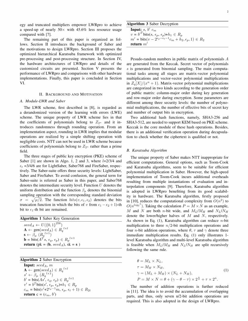
Fig. 1. Karatsuba multipliers array executing degree-d polynomial multipli-cation: P =M ×N .
III. KARATSUBA-BASED POLYNOMIAL MULTIPLICATION
LWRpro optimizes the hierarchical Karatsuba frameworkproposed in [27] to enable degree-256 polynomial multipli-cation in 81 cycles without considering pipeline startup time.Moreover, a hardware-efficient Karatsuba scheduling strategy,incorporating compact pre-processing circuits and several nec-essary modules, are developed to achieve high-performancecomputations with substantial overhead reduction.
A. Hierarchical Karatsuba Framework
Various types of Karatsuba systolic multipliers were exten-sively used in the implementations of ECC and RSA [23]–[26].Fig. 1 shows a fully parallel Karatsuba array correspondingto 1-level Karatsuba algorithm, following the optimizationmethod proposed in [11]. The architecture is able to executedegree-d polynomial multiplication each time, which consistsof three relatively small processing element arrays (PEAs) ex-ecuting degree-d/2 polynomial multiplication simultaneously.The Karatsuba algorithm consists of three phases: Pre-Add,multiplication and Post-Add. Pre-Add and Post-Add denoteall addition or subtraction operations performed before andafter multiplication in Karatsuba algorithm, respectively. Onelevel split of Karatsuba algorithm is able to reduce fourmultiplication operations to three, achieving a 25% reduction.This structure can be adopted recursively to save more multi-plication operations.
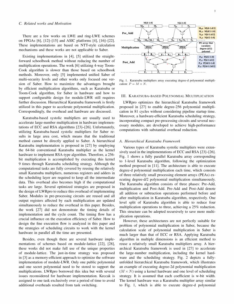
However, these architectures are not perfectly suitable forproblem of polynomial multiplication in Saber, because thecalculation scale of polynomial multiplication in Saber ismuch larger than that of ECC or RSA. Applying Karatsubaalgorithm in multiple dimensions is an efficient method toreuse a relatively small Karatsuba multipliers array. A hier-archical Karatsuba framework is used in [27] to acceleratethe large-number multiplication, including the kernel hard-ware and the scheduling strategy. Fig. 2 depicts a fully-unfolded hierarchical Karatsuba framework, which illustratesan example of executing degree-2d polynomial multiplication(M ×N ) using a kernel hardware and one level of schedulingstrategy. It is assumed that each coefficient is w-bit width.The kernel hardware was a Karatsuba multiplier array similarto Fig. 1, which is able to execute degree-d polynomial

4
Kernel
+RM
ML
Mux
MH
+RN
NL NH
e1e1 e0e0 f1f1 f0f0 d1d1 d0d0
r3r3 r2r2 r1r1 r0r0
+
+
+
+
MuxMux
Execution flow:1, RM←ML+MH;
RN← NL+NH;
2, P←ML×NL;
d1←PH; d0←PL;
3, P←MH×NH;
e1←PH; e0←PL;
4, P←RM×RN;
f1←PH; f0←PL;
5, r3←e1;
r2←f1+e0-e1-d1;
r1←f0+d1-e0-d0;
r0←d0;
d*w
+- -
-
P
(P: degree-2d intermediate result polynomial from the kernel; P = PL+PH×2d;
r=r0+r1×2d+r2×22d+r3×23d; : register group storing d coefficients;
w: coefficient bit width.)
-
d*w d*w d*w
2d*w
Fig. 2. Hierarchical Karatsuba hardware circuits calculating r =M ×N .
multiplication at one call. The scheduling structure includedpre-processing and post-processing circuits, before and afterthe kernel, corresponding to the Pre-Add and Post-Add phasesin the scheduling layer, respectively. The scheduling strategyis a specific algorithm that follows a finite-state machine toschedule the kernel hardware as the pseudo codes in Fig. 2.The selection signals of multiplexers and update enable signalsof registers are controlled by this finite-state machine. Andthe inverters to support subtraction operations are omitted inFig. 2, which is the same as Fig. 4 and Fig. 5. The finalmultiplication results are stored in register groups r3, r2, r1and r0 and each can store d/2 coefficients. The pseudo codesin this figure obeys to one level of Karatsuba algorithm and thescheduling strategy can be extended to obey to the Karatsubaalgorithm with multiple levels.
The work in [27] utilized a 2-level hierarchical Karatsubaframework similar to a fully-unfolded structure. Similarly, thiswork did not consider the module reusage of adders andregisters in the input side. Differently, there is one layer ofregisters reusage implemented in the output.
Hierarchical Karatsuba calculating framework is dividedinto two layers: kernel layer and scheduling layer. How tobalance the weights of two layers is an important topic forthe implementation of Saber. Although Karatsuba algorithmsin two layers can both reduce the number of multiplicationoperations to the same degree, kernel layer arranges multi-plication operations in a spatial parallel way and schedulinglayer arranges multiplication operations in a time sequentialway. When more levels of Karatsuba algorithm are arrangedin kernel layer, the number of multipliers increases. Corre-spondingly the latency decreases with the area and requiredbandwidth increase.
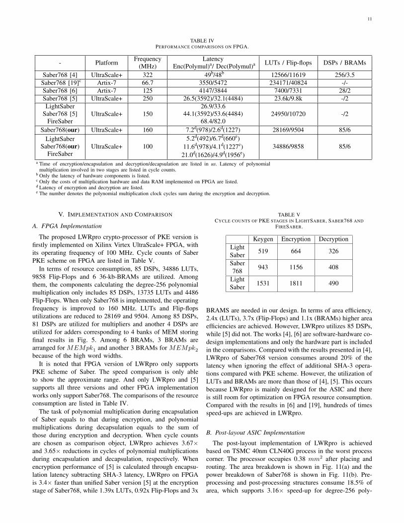
The main computational task in Saber is degree-256 poly-nomial multiplications. The design of kernel hardware inLWRpro is shown in Fig. 3, which is a 4-level recursiveversion of Fig. 1. Three phases of calculation are separatedby 2 rows of registers: RKA/RKB and RKC . Kernel Pre-Addand Kernel Post-Add circuits are strings of adders to formthe 4-level recursive adoption of the corresponding circuits inFig. 1. Kernel layer, consisting of 81 multipliers and additionaladders, is able to process degree-16 polynomial multiplicationat one call. Scheduling layer in LWRpro needs to transformfrom the original task in Saber, namely degree-256 polyno-mial multiplications, to the processing ability of the kernelhardware, namely degree-16 polynomial multiplications, inKaratsuba way. The algorithm of the whole hierarchical Karat-suba framework is illustrated in Algo. 4. The 16-coefficientvector input is transformed into Karatsuba input through pre-processing circuits, in the meantime pre-processing registersare updated. Kernel hardware processes the multiplication ofKaratsuba input and degree-64 sub-polynomial multiplicationresults are mapped onto 128-coefficient intermediate registerst through one part of the post-processing circuits. Then eachintermediate register is mapped on final results one by onethrough another part of post-processing circuits. The designdetails of pre-processing and post-processing structures inscheduling layer are demonstrated in the next two subsections.
Algorithm 4 Hierarchical Karatsuba framework for degree-256 polynomial multiplication in LWRpro
Input: A, B:degree-256 polynomial.Output: Res = A×B mod x256 + 1.for (i=1;i≤81;i++) do
. Pre-process:(PreRegA,αi′) ← Preprocess(PreRegA, InAi);(PreRegB,βi′) ← Preprocess(PreRegB, InBi);
. Kernel calculation:(PH ,PL) ← Kernel degree16mul(ai′,bi′);
. Post-process:(t7, t6,..., t0) ← Map2level(PH ,PL);if a degree-64 sub-polymul has done and j ≤ 7 then
j = 0;Res ← Res + Map2level serial(tj);j = j + 1;
end ifend forreturn Res
In hierarchical framework, 4 levels of Karatsuba algorithmare arranged in kernel layer and another 4 levels are arrangedin scheduling layer to achieve a better trade-off betweenlatency and area. The overall 8 levels of Karatsuba algorithmare able to convert the degree-256 polynomial multiplicationto the coefficient-wise multiplication. Each level of Karatsubaalgorithm reduce 25% of multiplications and 8 levels in LWR-pro saves up to 90% of multiplication operations, reducingthe coefficient-wise multiplication number in a degree-256polynomial multiplication from 65536 to 6521. When morelevels of Karatsuba algorithms are involved in the kernel hard-ware, 243 or more multipliers are needed, which is beyond the
5
mul
1
mul
2
mul
3 ...mul
80
mul
81
RKA1RKB1RKA2RKB2... RKA81RKB81
Kernel
Post-Add
RKC 1 2 3 ... 80 81
PH PL
mul
1
mul
2
mul
3 ...mul
80
mul
81
RKA1RKB1RKA2RKB2... RKA81RKB81
Kernel
Post-Add
RKC 1 2 3 ... 80 81
PH PL
b15...b3b2b1b0
RKB ...1 2 3 80 814 78 79RKB ...1 2 3 80 814 78 79
Kernel
Pre-Add
b15...b3b2b1b0
RKB ...1 2 3 80 814 78 79
Kernel
Pre-Add
Kernel
Pre-Add
a15...a3a2a1a0
RKA ...1 2 3 80 814 78 79RKA ...1 2 3 80 814 78 79
Kernel
Pre-Add
a15...a3a2a1a0
RKA ...1 2 3 80 814 78 79
...
a0 a15 a0
+a1
...
a14
+a15
a0+a1
+a2+a3
...
a12+a13
+a14+a15
a0+a1
+a2+a3
+a4+a5
+a6+a7
...
a8+a9
+a10+a11
+a12+a13
+a14+a15
1 16 17 48 49 72 73 80 81a0+a1
+...+a7
+a8+a9
+...+a15
...
a0 a15 a0
+a1
...
a14
+a15
a0+a1
+a2+a3
...
a12+a13
+a14+a15
a0+a1
+a2+a3
+a4+a5
+a6+a7
...
a8+a9
+a10+a11
+a12+a13
+a14+a15
1 16 17 48 49 72 73 80 81a0+a1
+...+a7
+a8+a9
+...+a15
...
a0 a15 a0
+a1
...
a14
+a15
a0+a1
+a2+a3
...
a12+a13
+a14+a15
a0+a1
+a2+a3
+a4+a5
+a6+a7
...
a8+a9
+a10+a11
+a12+a13
+a14+a15
1 16 17 48 49 72 73 80 81a0+a1
+...+a7
+a8+a9
+...+a15
... ... ...
Fig. 3. Kernel hardware of LWRpro based on 4-level Karatsuba algo-rithm. ai/bi: i-th coefficients in the sub-polynomial. PH /PL: degree-16 sub-polynomial. PH×x16+PL =
∑15i=0
∑ij=0 ajbi−j . RKA,RKB or RKC :
Registers for operand A, B or multiplication results.
reasonable area and correspondingly the bandwidth of memoryis too large. When more levels of Karatsuba algorithms areinvolved in scheduling layer, more complex pre-processingand post-processing structures are needed and the latency ishigher than the current design. This is the reason why sucha trade off is chosen in LWRpro. Compared with the designonly equipped with the kernel hardware, 4 levels in schedulinglayer reduces the cycle count from 256 to 81 to calculate adegree-256 polynomial multiplication in LWRpro, achieving a3.16× speed-up.
The structure of Karatsuba multipliers are relatively mature,so the overheads of the kernel hardware are relatively fixed.However, there is much space to discuss the structure and thecost of scheduling layer. For the convenience of comparison,the costs of fully-unfolded structure are assessed and the costsof partial-reusage structure in [27] are estimated naturallythrough deleting the corresponding layer of registers in outputside. And it is assumed that there is p-level Karatsuba algo-rithm in scheduling layer and the kernel hardware is able toprocess degree-d polynomial multiplication at one call. In theinput side, there are 3p d-coefficient intermediate terms gen-erated from p-level Karatsuba algorithm of scheduling layerand 2p terms are already in input memory for each polynomial.Besides, each register is equipped with a separate adder. So thearea of pre-processing registers (INreg) is estimated throughthe number of 1-coefficient registers and the area of pre-processing adders (INadd) is estimated through the numberof 1-coefficient input-width adders:
INreg ∝ 2× (3p − 2p)× d; (2)
INadd ∝ 2× (3p − 2p)× d. (3)
r3r3 r2r2 r1r1 r0r0
+
MuxMux MuxMux
PH PL-
1, P←ML×NL;
r0←PL; r1←PH-PL;
r2←-PH;
2, P←MH×NH;
r3←PH; r2←r2-(PH-PL);
r1←r1-PL;
3, P←RM×RN;
r2←r2+PH; r1←r1+PL;
+ +
...
(P: degree-2d result polynomial from the kernel, P = PL+PH×2d)
Fig. 4. Post-processing in scheduling layer with 1-level SHEKS.
In the output side of 1-level scheduling structure as (shownin Fig. 2, p = 1), there are 3 sets of registers and each setconsists of 2p d-coefficient registers. There are 5× 2p−1 × d1-coefficient input-width adders to generate the final results.When the scale of computational task increases and one morelevel of Karatsuba algorithm is added in scheduling layer,triple more sets of registers and half of register groups in eachset are needed in the new level. It is the same for the adders.According to the same estimation method, the numbers ofpost-processing registers (OUTreg) and post-processing adders(OUTadd) are estimated as:
OUTreg ∝p∑i=1
3i × 2p−i+1 × d; (4)
OUTadd ∝p∑i=1
5× 3i−1 × 2p−i × d. (5)
When p ≥2, for example p = 4 in this paper, the overheads ofscheduling layer becomes much larger. So more efficient pre-processing and post-processing structures are necessary, whichare presented in Section III-B and Section III-C.
B. Sequential Hardware-Efficient Karatsuba Scheduling
In the hierarchical Karatsuba framework, post-processingstructure is used to temporarily store the multiplication resultsto support Post-Add stage in the scheduling layer. Sequentialhardware-efficient Karatsuba scheduling (SHEKS) strategy isproposed to optimize this overhead.
The main goal of SHEKS is to allow each multiplication inthe Karatsuba algorithm to completely affects the final resultswithout additional registers. In Fig. 2, the final values in r1, r2are influenced by all three multiplications. This is due to theeffect of Post-Add stage of Karatsuba algorithm in schedulinglayer. If all the addresses in the results of each multiplicationare already preassigned and allow each multiplication resultto spread to all affected locations, then additional registers areno longer needed. The SHEKS version of Fig. 2 is shown inFig. 4. The results of each multiplication pass through differentpaths and influence the corresponding result registers.
Compared with Fig. 2, Fig. 4 saves all six 16-coefficientregister groups, d e f , and two adder groups with a width of

6
+
PH PL
+
t7t7 t6t6 t1t1 t0t0
+
MuxMux
+
Mux
+
MuxMux
+
Mux
…
MEM
I
+
MEM
II
+
MEM
III
+
MEM
IV
+
…
During a
degree-64
polymul
-
…
(t: temporal registers set storing the degree-128 polynomial results of degree-64 polymul.
ti: degree-16 subpolynomial; t = t0+t1×2d+t2×2
2d+...+t7×2
7d)
1, t0→ MEM;
2, t1→ MEM;
3, t2→ MEM;
4, t3→ MEM;
5, t4→ MEM;
6, t5→ MEM;
7, t6→ MEM;
8, t7→ MEM;
...
During
another
degree-64
polymul
Mapping operation
Fig. 5. The output side of scheduling layer in LWRpro with 4-level Karatsubaalgorithm.
16-coefficient. The additional overhead is some multiplexers.The idea of SHEKS can be extended to more levels ofKaratsuba algorithm in scheduling layer and the overheads canbe estimated. All result register groups except for the leftmostand rightmost ones need a corresponding accumulation addergroup. Besides, 2 adder groups computing intermediate values,PH -PL and PH+PL, are needed when p ≥ 2. So the overheadsare:
OUTreg ∝ 0; (6)
OUTadd ∝ 2p+1 × d. (7)
For the implementation of Saber, p=4 and the number ofadders in a direct application of SHEKS is a little higher.Moreover, a subtraction polynomial operation on the finalresults is needed because there is a modular polynomialxn + 1, more adders are needed. So a new layer of registersis inserted in LWRpro to temporarily store the degree-64sub-polynomial multiplication results and the values are thenmapped to the final memory one by one. Table I lists themapping rules of the SHEKS structure with 2-level Karatsubaalgorithm to calculate degree-64 polynomial multiplication,namely Map2level function in Algo. 4. And the structure isshown in Fig. 5.
When one degree-64 polynomial multiplication is executed,the temporary results are stored in the register group array t.During this period of time, the values of one register groupare mapped to final memory in each cycle following theSHEKS rules, too. Differently, the mapping mechanism isserial, which is different from the parallel way in Fig. 4. Andthe mapping rules vary among different degree-64 polynomialsin a degree-256 polynomial following a serial version ofTable I, namely Map2level serial function in Algo. 4. Themapping time of 8 cycles is completely hidden by the degree-64 multiplication time of 9 cycles. Moreover, The polynomialsubtraction operation of the final results are added to themapping rule and it is executed during the mapping operation.
To fulfill pipelining and eliminate the bubbles for waiting,2 additional register groups are needed, which is not shownin Fig. 5. It has been considered in the overhead estimationin the end of Section III-C. The post-processing timetable and
Kernel
+Mux
Mux
Mux
Mux
R0R0 R1R1
0
MuxMux MuxMux
0
…
+
+Regout
MuxMux MuxMux
R2R2 0 0
INRDWR
InputMEM
Conv64_16
Conv128_64 Conv256_128
i3 i4
i1 i2
out
dim
MuxMux
0
4-level pre-process:
Arrα1′ ←Conv128_16(α0,..,α7);
WR←Conv256_128(α0,..,α7);//27 cycles
Arrα2′ ←Conv128_16(α8,..,α15);
WR←Conv256_128(α8,..,α15,RD);//27 cycles
Arrα3′ ←Conv128_16(α0+α8,..,α7+α15)://27
cycles
3-level pre-process:
Arrα1′←Conv64_16(Conv128_64((α0,..,α3));
//9 cycles
Arrα3′←Conv64_16(Conv128_64((α0,..,α3,..,α7));
//9 cycles
Arrα2′←Conv64_16(Conv128_64((α4,..,α7));
//9 cycles
Arrα′: Karatsuba input array of the sub-polynomials in
the input polynomial.
Subscript corresponding to the sub-polynomials:
1: former degree-half sub-polynomial
2: latter degree-half sub-polynomial
3: sum of 1 and 2
Fig. 6. Optimized pre-processing design of Saber with 4-level Karatsubaalgorithm.
mapping timetable are determined based upon the rules asdiscussed above and the input order discussed in Section III-C.
C. Compact Input Pre-Processing
A compact input pre-processing technique is utilized inLWRpro to reduce the number of registers and adders re-quired in pre-processing of scheduling layer. Registers in pre-processing circuits are needed to store two types of data:the input from input memory and the intermediate resultsgenerated from the pre-processing. The optimization madein this paper is to reuse the registers and adders. Based onour observations, storing some inputs is enough to reducethe memory accesses and eliminate additional latency ofthe reading operations. Moreover, the execution order of themultiplications is reorganized to maximize the reusability ofdata stored in the input registers. We take 2-level Karatsubaalgorithm in the scheduling layer as an example, and thecompact pre-processing structure is shown as Conv64 16 inFig. 6, which is part of the whole pre-processing circuits ofour design. This module converts the input from a degree-64polynomial to nine degree-16 polynomials in Karatsuba way.
The pre-processing for the two polynomial multiplicationoperands is identical. For simplicity, only the pre-processingof operand A is discussed in this section, as it is alsoapplicable to the other operand B. Table II provides theoperation details of Fig. 6 in cycles, where ai is the i-thdegree-16 polynomial in A and A =
∑3i=0 αi × x16i. Nine
cycles are needed to calculate a degree-64 sub-polynomialmultiplication. Pre-processing register groups R0 and R1 areused to cache some inputs or outputs to support future additionoperations calculating Karatsuba intermediate values. Theseregisters eliminate the additional bubble cycles of waiting forreading the second operand values of addition operation andstore some intermediate values. The input order from inputmemory is re-organized to maximize the reusability. Only 1adder group and 2 register groups with 16 1-coefficient widthare needed in module Conv64 16. Compared with the fully-unfolded structure, 4 adder groups and 3 register groups aresaved, while extra multiplexers are required.
For the implementation of Saber, the task of the pre-processing structure is to convert the multiplication operationswith degree-256 polynomials to the operations with degree-16

7
TABLE IPOST-PROCESSING MAPPING TABLE OF 2-LEVEL KARATSUBA ALGORITHM.
t0 t1 t2 t3 t4 t5 t6 t7α0×β0 +PL +PH -PL -PH -PL -PH+PL +PH
(α0+α1)×(β0+β1) +PL +PH -PL -PHα1×β1 -PL -PH+PL +PH+PL +PH -PL -PHα2×β2 -PL -PH+PL +PH+PL +PH -PL -PH
(α2+α3)×(β2+β3) -PL -PH +PL +PHα3×β3 +PL +PH -PL -PH -PL -PH+PL +PH
(α0+α2)×(β0+β2) +PL +PH -PL -PH(α0+α1+α2+α3)× (β0+β1+β2+β3) +PL +PH
(α1+α3)×(β1+β3) -PL -PH+PL +PHαi, βi denote the i-th degree-16 sub-polynomial in a degree-256 polynomial of operand A and B, respectively.
TABLE IITHE PRE-PROCESSING CYCLES TIMETABLE OF CONV64 16 IN FIG. 6.
dim i1 i2 out R0 R1
1 α0 α0 0 α0 X X2 α1 α1 0 α1 α0 X3 α1 α1 α0 α0+α1 α0 X4 α2 α2 0 α2 α0 X5 α2 α2 α0 α0+α2 α0 X6 α3 α3 0 α3 α2 α0+α2
7 α3 α3 α2 α3+α2 α2 α0+α2
8 α1 α1 α3 α3+α1 α3 α0+α2
9 X α0+α2 α1+α3α0+α1+α2+α3
α1+α3 α0+α2
αi denotes the i-th degree-16 sub-polynomial in a degree-256polynomial of operand A and B, respectively.
polynomials that the kernel hardware is able to process. Thecorresponding pre-processing circuit is shown in Fig. 6 andhow the 4-level pre-processing is constructed is depicted inthe pseudo-algorithm of this figure.
It requires 81 cycles with several additional pipeline ini-tialization cycles to 4-level pre-processing. The first 27 cyclesare needed to calculate the former degree-128 sub-polynomialmultiplication, the second 27 cycles are needed to calculatethe latter degree-128 sub-polynomial multiplication, the last27 cycles are needed to calculate the sum polynomial of theformer and the latter degree-128 sub-polynomial multiplica-tion. In Fig. 6, Part Conv256 128 executes the correspondingpolynomial addition operations. During the first 27 cycles, thecorresponding read values are written into an additional inputmemory. During the second 27 cycles, the polynomial sumoperation is executed and the sum results are written backto the additional input memory to support sum polynomialmultiplication during last 27 cycles. The second 27 cyclesand last 27 cycles’ timetables are the same as the first 27cycles’ timetable except for RD and WR values. Among each27 cycles, the first 9 cycles are needed to calculate the formerdegree-64 sub-polynomial multiplication as the same orderof Table II, the second 9 cycles are needed to calculatethe sum polynomial multiplication, and the last 9 cyclesare needed to calculate the latter degree-64 sub-polynomial
2080 2080
6240
5200
2080 2080
3648
5200
38496 160 192
0
1000
2000
3000
4000
5000
6000
7000
OUTadd
Num
of R
egis
ters
or
Add
ers
OUTreg
Partial-reused Method[27]
INreg INadd
Fully-unfolded Method
SHEKS and Compact preprocess
5.9x 21.7x
22.8x
27.1x
Fig. 7. Resource usage comparison
multiplication. In Fig. 6, Part Conv128 64 executes the cor-responding conversion job from a degree-128 polynomial tothree degree-64 polynomials in Karatsuba way. Table III showa timetable example of Part Conv128 64 for pre-processingto obtain sum sub-polynomial during first 27 cycles with thehelp of R2 and Regout. The output is organized in the orderrequired by Part Conv64 16. The complete 27-cycle timetableis easy to obtain because first 9 cycles and last 9 cycles’ pre-processing are simpler without sum operation of degree-64polynomials. Register R2 stores some values to support thepolynomial addition operation. Register Regout not only playsthe role of pipeline register, but also helps to latch values forthe next cycle. Part Conv64 16 converts from the degree-64polynomial into degree-16 polynomials in Karatsuba way, asdescribed above.
To sum up, as shown in Fig. 7, compared with thestraightforward implementation without reusage and partial-reusage method in [27], this proposed architecture has morecompact pre-processing and post-processing architectures interms of registers and adders utilization. This improvement isachieved via utilizing two proposed techniques: SHEKS andcompact input structure. The area consumption is evaluated bythe number of 1-coefficient registers and 1-coefficient input-width adders. The overheads of straightforward fully-unfoldedmethod are calculated by Eq. 2, Eq. 3, Eq. 4 and Eq. 5.The overhead of [27] is estimated through deleting one layerof post-processing registers. Fig. 5 and Fig. 6 depict theoverheads of LWRpro. Besides, the additional input memory

8
TABLE IIIINPUT STREAM TIMETABLE OF PRE-PROCESSING STRUCTURE.
Cycle in R2 i3 i4 dim Regout out WR RD9 α4 α0 α0 α4 α0+α4 - - α4
10 α1 α0 0 0 0 α0+α4 -11 α5 α1 α1 α5 α1+α5 α0+α4 - α5
12 α2 α1 0 0 0 α1+α5 α0+α4
13 α6 α2 α2 α6 α2+α6 α1+α5 α1+α5 α6
14 α3 α2 0 0 0 α2+α6 α0+α1+α4+α5
15 α7 α3 α3 α7 α3+α7 α2+α6 α6 α7
16 α1 α3 0 0 0 α3+α7 α0+α2+α4+α6
17 α5 α1 α1 α5 α1+α5 α3+α7 α7
18 - α5 0 0 0 α1+α5 α3+α2+α6+α7
19 α4 α5 0 α4 α4 α1+α5 α3+α1+α7+α4
20 - α5 α5 0 α5 α4 α0+α1+α2+α3+α4+α5+α6+α7
and 2 group of output pipeline registers are also considered.Fig. 7 shows the overhead comparisons of pre-processingregisters, pre-processing adders, post-processing registers andpost-processing adders. Up to 90.5% of the registers are nolonger required with the adoption of the proposed meth-ods, while 96.0% of the reductions are achieved regardingthe adders, which is benefited from the higher reusgae andparallelism. Most of the costs in the scheduling layer arecompressed and these techniques improve the usability of thehierarchical calculating framework of Karatsuba algorithm.
IV. HARDWARE ARCHITECTURE
A. System Architecture and Configurable Design
Fig. 8 shows the system architecture of LWRpro. MemoryKEMkey and KEMcipher marked in green stores key-relateddata and ciphertext-related data as input and output of SHA-3 functions to support KEM scheme, respectively. MemoryKEMkey and KEMcipher are organized as two single-portRAMs and there is a wrapper on these two RAMs for unifiedaddress space. Plaintext, ciphertext and key data pass throughbetween memory KEMkey/KEMcipher and the PKE mod-ule. Data are organized in memory KEMkey/KEMcipher forKeccak module marked in blue to execute SHA-3 functions.During decapsulation, ciphertext are imported into KEMcipherand compared in verify module marked in purple with anotherciphertext from re-encryption operation in PKE module. Thecomparison operation is parallel with PKE executions, whichhides the latency overheads. The verification results only affectthe input address of memory KEMkey/KEMcipher for thefollowing SHA-3 operations. In PKE part, public matrix isgenerated from Keccak module and imported into memorymarked in green after alignment. Secret vector is generatedfrom sampler marked in orange and imported into inputmemory. Polynomial multiplications are executed in multipli-cation part marked in yellow and the results are exported tooutput memory marked in green. Before output, the resultsneeds addition operations in adder array and bits truncationoperations in Trunc part.
PreA and PreB represent the input pre-processing cir-cuits of operand A and operand B in scheduling layer,
and Post denotes the post-processing components. MEMpkand MEMsk denote memory storing data of public key anddata of secret key, respectively. MEMtmp denotes memorystoring the intermediate results and final results of polynomialmultiplication. MEMsk and MEMtmp are divided into fourbanks to store four polynomials of the secret key and theintermediate values for all three versions of Saber. MEMpkis divided into two banks to serve as an input ping-pongbuffer to enable pipelining. All PKE memories are organizedas register files and memories are double-port to support writeand read simultaneously. The align part is used to handle thedata alignment. According to the specification for Saber, thebinomial sampler is implemented in a straightforward manner.High-speed Keccak module comprises two Keccak-f parallelhardware and supports two Keccak-f[1600] computations percycle. Each copy of Keccak-f hardware is implemented in astraightforward way [29]. Therefore each round of Keccak isexecuted every 12 clock cycles.
The multiplier array is reused to support both vector-vectorand matrix-vector multiplication. The Keccak module is sharedto generate both public and secret key pairs. The adder arrayfollowing MEMtmp in Fig. 8 is shared by encryption anddecryption. It consists of four adders to facilitate additionoperations for all three versions of Saber, which processes fourterms of the polynomial at each output. The array is shown inthe upper right corner of Fig. 8.
To achieve a configurable design among all the securitylevels and stages of Saber, some configurable design ideas areadopted. Some modules can be reused, such as multiplicationhardware and Keccak hardware, but parameter choices needto be redundant for all variants of Saber, such as bank numberof MEMsk and sk-input width of multipliers. The adder arraybefore truncation, which is illustrated in the upper right cornerof Fig. 8, also adopts the configurable design among differentstages and security levels with the help of multiplexers.However, this idea does not work in some components. Thesecomponents, including data alignment modules and outputtruncation modules, adopt the idea of multi-parameter design.The data alignment modules are illustrated in the lower rightcorner of Fig. 8. The four data aligning modules execute

9
Multiplier
Array
PreA PreB
Po
st
MEMpk MEMsk
MEMtmp
Ali
gn
208
64208
208 64
64
Sampler
Multiplication
RST CLK SDO DODI
Memory
KeccakKeccak
Adder
ArrayTruncTruncTrunc
Adder
ArrayTruncTrunc
PRNG
(Keccak)
Binomial
Sampler
Binomial
Sampler
=Verify
=Verify
PKE
SDI
KEMkeyKEM
cipherKEMkey
KEM
cipher64
PRNG
and
Hash
64
AdderAdder
v’’
Adder
10
10MU
XM
UX
MU
X
MU
XM
UX
MU
X
v’h1
h2
cm’m’
++
-
10
10MU
X
MU
X
v’h1
h2
cm’m’
++
-
AdderAdderAdder
v’’
Adder
10
10MU
X
MU
X
v’h1
h2
cm’m’
++
-
Adder
Align_208
MU
X Binomial
Sampler
InputReg
BitSelect
OutReg208
Public key1344
BitSelect
Reserve
Reg
Align_160
Align_128
Align_96
Align_64 KEMkey
Align_208
MU
X Binomial
Sampler
InputReg
BitSelect
OutReg208
Public key1344
BitSelect
Reserve
Reg
Align_160
Align_128
Align_96
Align_64 KEMkey
Align Part
addr
Fig. 8. The system architecture of LWRpro crypto-processor.
different types of data aligning jobs. For example, Align 208module arranges a 1344-bit input and achieves a 208-bitoutput. At each cycle, BitSelect chooses the corresponding bitsfrom InputReg and ReserveReg part to write to ReserveRegand OutReg. The truncation modules adopt the same idea.Multiple truncation modules execute different truncation jobsof output with different bit numbers and packing jobs.
B. Task-rescheduling-based Pipeline Design
The computational operations involved in Saber are finelyscheduled to enable high-performance processing from thehardware designer’s perspective. Moreover, some pipelinetricks are added to reduce the time overheads of data importingbefore polynomial multiplication and data exporting afterpolynomial multiplication as much as possible.
In hardware implementation, the Keccak is utilized togenerate polynomials of the public key and the secret key.To ensure that the Keccak is able to focus on one job over aperiod of time, the execution order in the software [3] shouldbe reconsidered. Saber768 is taken as an example, and Fig. 9shows the circuit design and execution flow of LWRpro. Thenumber after MEM in Fig. 9 denotes the bank index of theMEM. MEMtmp is also divided in another way accordingto memory address into 4 pieces: MEMtmp1, MEMtmp2,MEMtmp3 and MEMtmp4, which are abbreviated as Tmp1,Tmp2, Tmp3 and Tmp4.
For matrix-vector multiplication in Saber, all polynomialsof the secret key, such as B1, B2 and B3, are generatedin advance. Polynomials of public key, such as A1, A2 andA3, are generated in pipeline and the generation is parallelwith the multiplication hardware to reduce the whole latencyoverheads and memory size storing public polynomials. Themultiplication operations A1 ×B1, A2 ×B2 and A3 ×B3 ...are carried out once the corresponding public polynomials are
ready. For vector-vector multiplication, the polynomials of thepublic key and the secret key are generated in parallel. This isbecause public polynomials are imported from the interface.
Martix-vector and vector-vector polynomial multiplicationsare both involved in encryption stage. Vector-vector multi-plication is scheduled before matrix-vector multiplication inLWRpro to avoid the additional timing overhead of loadingthe vector of the secret key.
While one polynomial of the public key is used in polyno-mial multiplication, the next polynomial is imported to anotherbank of MEMpk. This reduces the data importing time ofmultiple polynomials and the multiplication hardware keepsrunning once activated as shown at the bottom of Fig. 9.The same holds for the reduction in data exporting time,because MEMtmp has more than one bank. For matrix-vectorpolynomial multiplication during encryption, the first pieceTmp1 and the second piece Tmp2 serves as an output ping-pong buffer, which allows data exporting from MEMtmp isable to execute in parallel with the multiplication.
As shown at the right corner of Fig. 9, the multiplicationA1 × B1 during vector-vector polynomial multiplication isstarted as long as parts of the operands A1 and B1 have beenloaded into the MEM. By implementing this trick, 40 cyclesare reduced in the vector-vector multiplication process, whichimproves the efficiency of decryption. For key generation,public matrix is generated in column-major order and it isinconsistent with the matrix-vector multiplication order. Soall four result polynomials of FireSaber need to be stored inMEMtmp temporarily during matrix-vector multiplication inkey generation.
To sum up, MEMpk and MEMtmp are used as ping-pong buffers in the task-level pipeline. Besides, the multi-bank design also plays other roles. Four banks of MEMtmpare needed to store multiple result polynomials during key

10
Multiplication
Hardware(Kernel and
preprocessing and
post-processing
circuits)
MEMpk1
MEMsk1
MEMsk2
MEMsk3
MEMsk4
MEMsk1
MEMsk2
MEMsk3
MEMsk4
MEMpk2
IIIIII
III
III
IVIV
MEMtmp1
MEMtmp
Tmp2 Tmp3 Tmp4
Generation and
import to MEM:
Multiplication:
A1B1 B2 B3
A1×B1 ...A1
B1
A2×B2 A3×B3
Matrix-Vector Multiplication in Encryption Vector-Vector Multiplication
Write to MEMtmp:
A4×B1
Tmp1
..
Generation and
import to MEM:
Multiplication:
Column-major Matrix-Vector Multiplication in Key Generation
Write to MEMtmp:
..
A2 A3 A4
Tmp2
A1B1 B2 B3
A1×B1 ...A2×B1 A3×B1 A4×B2
Tmp1
...A2 A3 A4
Tmp2 Tmp3 Tmp1 ...
Tmp1
A1×B1 A2×B2 A3×B3
A2
B2
A2
B2
Execution order
Keccak
Keccak
or
Interface
Ai/Bi: i-th degree-
256 polynomial in
public
matrix/secret vctor
Pipelining
hardware
Fig. 9. Task-rescheduling pipeline hardware and execution flow of Saber768.
generation. Hardware reusage can reduce the overheads oftask-level pipeline.
C. Truncated MultiplierThe work in [5] utilized addition operations and look-up
table to perform multiplication operations for Saber. However,this method is only suitable for the schoolbook multiplication.For Karatsuba multiplications, truncated multipliers for Saberare adopted in LWRpro utilizing the properties of binomialsampling and LWR algorithms.
For a random number sequence generated by the Keccakmodule, the binomial sampler divides the input sequence intosubsequences with consecutive µ bits. The Hamming weightsof the higher half and lower half of the i-th subsequence arecalculated and stored alternatively into registers denoted as aiand bi. Then, secret key si is obtained by:
si = (ai − bi) mod q. (8)
For Saber768, µ = 8 means that ai and bi have a value rangeof [0, 4]; in other words, the difference of these two operandshas a value range of [−4, 4]. For previous software imple-mentations, si is extended to 13 bits through sign extensions.However, not all 13 bits are needed to calculate the final result.Let si′ = ai − bi without modular operation; if si′ ≥ 0, thensi′ = si; if si′ < 0, then si×r mod q = (si
′+q)×r mod q =(si′ × r) mod q, where r denotes an arbitrary integer. Thus,
multiplications with 13-bit unsigned si can be replaced bysigned operations with 4-bit signed si′. It is noticed that only4 bits out of all 13 bits are useful in the calculation, whichmeans that the width of one operand for the multiplier canbe reduced to 4 bits. The storage and transmission of privatekeys are also benefited from the reduction in effective bits.
Instead of the modular operation of LWE, the round op-eration of LWR allows us to trim unnecessary operations.
154.2170.1
225.7 225.2
279.9267.6
316.8328.9 336.3 331.4
150
200
250
300
350
400
4-bit 5-bit 6-bit 7-bit 8-bit 9-bit 10-bit 11-bit 12-bit 13-bit 13-bit*
Are
a(u
m^
2)
bit-wdith of sk-related operator
13-bit*:13-bit x 13-bit with 26-bit output
618.0
Fig. 10. Area consumption comparisons among different input bit-widths.
Considering that the parameter q of Saber is 8192, i.e., onlythe lowest 13 bits in the result are kept, all multiplicationoperations unrelated to generating the lowest 13 bits in theresult can be avoided. The adoption of truncated multipliersdoes not affect the correctness of results and still conforms tothe specification of Saber. Fig. 10 shows the area of multiplierswhose widths of the secret key-related operand vary. All dataare collected under TSMC 40nm process, which is the same asthe process of LWRpro. 13-bit* denotes the full-size multiplierwith all 26-bit output. As Fig. 10 shows, truncated multipliersonly occupy 25% - 50% area of the full-size multiplier.
However, the effectiveness of this technique is limited by thePre-Add phase in the kernel hardware and the scheduling layer.Because the addition operations in the Pre-Add phase expandthe number of effective bits of the operand. This limitation isacceptable because at least 90% multiplication operations aresaved through 8-level Karatsuba algorithm.
11
TABLE IVPERFORMANCE COMPARISONS ON FPGA.
- Platform Frequency(MHz)
LatencyEnc(Polymul)a/ Dec(Polymul)a LUTs / Flip-flops DSPs / BRAMs
Saber768 [4] UltraScale+ 322 49b/48b 12566/11619 256/3.5Saber768 [19]c Artix-7 66.7 3550/5472 234171/40824 -/-Saber768 [6] Artix-7 125 4147/3844 7400/7331 28/2Saber768 [5] UltraScale+ 250 26.5(3592)/32.1(4484) 23.6k/9.8k -/2LightSaber
Saber768 [5]FireSaber
UltraScale+ 15026.9/33.6
44.1(3592)/53.6(4484)68.4/82.0
24950/10720 -/2
Saber768(our) UltraScale+ 160 7.2d(978)/2.6d(1227) 28169/9504 85/6LightSaber
Saber768(our)FireSaber
UltraScale+ 1005.2d(492)/6.7d(660e)
11.6d(978)/4.1d(1227e)21.0d(1626)/4.9d(1956e)
34886/9858 85/6
a Time of encryption/encapsulation and decryption/decapsulation are listed in us. Latency of polynomialmultiplication involved in two stages are listed in cycle counts.
b Only the latency of hardware components is listed.c Only the costs of multiplication hardware and data RAM implemented on FPGA are listed.d Latency of encryption and decryption are listed.e The number denotes the polynomial multiplication clock cycles sum during the encryption and decryption.
V. IMPLEMENTATION AND COMPARISON
A. FPGA Implementation
The proposed LWRpro crypto-processor of PKE version isfirstly implemented on Xilinx Virtex UltraScale+ FPGA, withits operating frequency of 100 MHz. Cycle counts of SaberPKE scheme on FPGA are listed in Table V.
In terms of resource consumption, 85 DSPs, 34886 LUTs,9858 Flip-Flops and 6 36-kb-BRAMs are utilized. Amongthem, the components calculating the degree-256 polynomialmultiplication only includes 85 DSPs, 13735 LUTs and 4486Flip-Flops. When only Saber768 is implemented, the operatingfrequency is improved to 160 MHz. LUTs and Flip-flopsutilizations are reduced to 28169 and 9504. Among 85 DSPs,81 DSPs are utilized for multipliers and another 4 DSPs areutilized for adders corresponding to 4 banks of MEM storingfinal results in Fig. 5. Among 6 BRAMs, 3 BRAMs arearranged for MEMpk1 and another 3 BRAMs for MEMpk2because of the high word widths.
It is noted that FPGA version of LWRpro only supportsPKE scheme of Saber. The speed comparison is only ableto show the approximate range. And only LWRpro and [5]supports all three versions and other FPGA implementationworks only support Saber768. The comparisons of the resourceconsumption are listed in Table IV.
The task of polynomial multiplication during encapsulationof Saber equals to that during encryption, and polynomialmultiplications during decapsulation equals to the sum ofthose during encryption and decryption. When cycle countsare chosen as comparison object, LWRpro achieves 3.67×and 3.65× reductions in cycles of polynomial multiplicationsduring encapsulation and decapsulation, respectively. Whenencryption performance of [5] is calculated through encapsu-lation latency subtracting SHA-3 latency, LWRpro on FPGAis 3.4× faster than unified Saber version [5] at the encryptionstage of Saber768, while 1.39x LUTs, 0.92x Flip-Flops and 3x
TABLE VCYCLE COUNTS OF PKE STAGES IN LIGHTSABER, SABER768 AND
FIRESABER.
Keygen Encryption DecryptionLightSaber 519 664 326
Saber768 943 1156 408
LightSaber 1531 1811 490
BRAMS are needed in our design. In terms of area efficiency,2.4x (LUTs), 3.7x (Flip-Flops) and 1.1x (BRAMs) higher areaefficiencies are achieved. However, LWRpro utilizes 85 DSPs,while [5] did not. The works [4], [6] are software-hardware co-design implementations and only the hardware part is includedin the comparisons. Compared with the results presented in [4],LWRpro of Saber768 version consumes around 20% of thelatency when ignoring the effect of additional SHA-3 opera-tions compared with PKE scheme. However, the utilization ofLUTs and BRAMs are more than those of [4], [5]. This occursbecause LWRpro is mainly designed for the ASIC and thereis still room for optimization on FPGA resource consumption.Compared with the results in [6] and [19], hundreds of timesspeed-ups are achieved in LWRpro.
B. Post-layout ASIC Implementation
The post-layout implementation of LWRpro is achievedbased on TSMC 40nm CLN40G process in the worst processcorner. The processor occupies 0.38 mm2 after placing androuting. The area breakdown is shown in Fig. 11(a) and thepower breakdown of Saber768 is shown in Fig. 11(b). Pre-processing and post-processing structures consume 18.5% ofarea, which supports 3.16× speed-up for degree-256 poly-
12
TABLE VIPERFORMANCE OF KEM STAGES IN LIGHTSABER, SABER768 AND
FIRESABER.
Keygen Encapsulation DecapsulationCyc-les
Power(mW)
Cyc-les
Power(mW)
Cyc-les
Power(mW)
LightSaber 603 35.7 859 37.2 1075 33.8
Saber768 1066 39.2 1456 41.3 1701 35.3
FireSaber 1716 44.8 2185 44.0 2478 42.1
Sampler
0.30% Keccak
15.70%
Memory
PKE
19.70%
Memory
KEM
4.20%
Mul_arr
ay
35.50%
Pre and
Post
22.30%
Others
2.30%
Sampler
0.40% Keccak
17.30%
Memory
PKE
30.30%
Memory
KEM
7.10%
Mul_array
21.20%
Pre and Post18.5%
Others
5.20%
(a) (b)
Fig. 11. Area breakdown(a) and power breakdown during encryption ofSaber768(b).
nomial multiplication. The number of equivalent gates ofLWRpro is 446.8k, which includes the hardware componentsexecuting logic operations and memory. The maximum op-erating frequency is up to 400 MHz with an average powerconsumption of 39 mW. Power is simulated through PTPxbased on real netlist simulation waveforms. The detailedimplementation results are listed in Table VI.
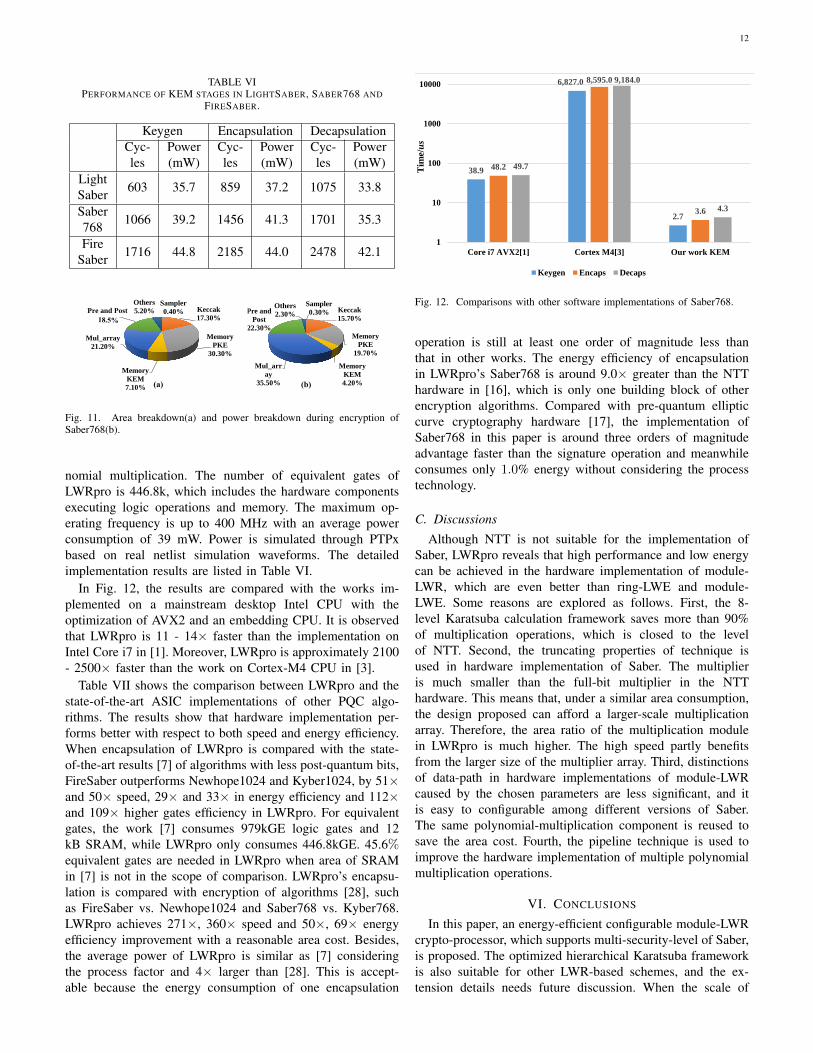
In Fig. 12, the results are compared with the works im-plemented on a mainstream desktop Intel CPU with theoptimization of AVX2 and an embedding CPU. It is observedthat LWRpro is 11 - 14× faster than the implementation onIntel Core i7 in [1]. Moreover, LWRpro is approximately 2100- 2500× faster than the work on Cortex-M4 CPU in [3].
Table VII shows the comparison between LWRpro and thestate-of-the-art ASIC implementations of other PQC algo-rithms. The results show that hardware implementation per-forms better with respect to both speed and energy efficiency.When encapsulation of LWRpro is compared with the state-of-the-art results [7] of algorithms with less post-quantum bits,FireSaber outperforms Newhope1024 and Kyber1024, by 51×and 50× speed, 29× and 33× in energy efficiency and 112×and 109× higher gates efficiency in LWRpro. For equivalentgates, the work [7] consumes 979kGE logic gates and 12kB SRAM, while LWRpro only consumes 446.8kGE. 45.6%equivalent gates are needed in LWRpro when area of SRAMin [7] is not in the scope of comparison. LWRpro’s encapsu-lation is compared with encryption of algorithms [28], suchas FireSaber vs. Newhope1024 and Saber768 vs. Kyber768.LWRpro achieves 271×, 360× speed and 50×, 69× energyefficiency improvement with a reasonable area cost. Besides,the average power of LWRpro is similar as [7] consideringthe process factor and 4× larger than [28]. This is accept-able because the energy consumption of one encapsulation
38.9
6,827.0
2.7
48.2
8,595.0
3.6
49.7
9,184.0
4.3
1
10
100
1000
10000
Core i7 AVX2[1] Cortex M4[3] Our work KEM
Tim
e/us
Keygen Encaps Decaps
Fig. 12. Comparisons with other software implementations of Saber768.
operation is still at least one order of magnitude less thanthat in other works. The energy efficiency of encapsulationin LWRpro’s Saber768 is around 9.0× greater than the NTThardware in [16], which is only one building block of otherencryption algorithms. Compared with pre-quantum ellipticcurve cryptography hardware [17], the implementation ofSaber768 in this paper is around three orders of magnitudeadvantage faster than the signature operation and meanwhileconsumes only 1.0% energy without considering the processtechnology.
C. Discussions
Although NTT is not suitable for the implementation ofSaber, LWRpro reveals that high performance and low energycan be achieved in the hardware implementation of module-LWR, which are even better than ring-LWE and module-LWE. Some reasons are explored as follows. First, the 8-level Karatsuba calculation framework saves more than 90%of multiplication operations, which is closed to the levelof NTT. Second, the truncating properties of technique isused in hardware implementation of Saber. The multiplieris much smaller than the full-bit multiplier in the NTThardware. This means that, under a similar area consumption,the design proposed can afford a larger-scale multiplicationarray. Therefore, the area ratio of the multiplication modulein LWRpro is much higher. The high speed partly benefitsfrom the larger size of the multiplier array. Third, distinctionsof data-path in hardware implementations of module-LWRcaused by the chosen parameters are less significant, and itis easy to configurable among different versions of Saber.The same polynomial-multiplication component is reused tosave the area cost. Fourth, the pipeline technique is used toimprove the hardware implementation of multiple polynomialmultiplication operations.
VI. CONCLUSIONS
In this paper, an energy-efficient configurable module-LWRcrypto-processor, which supports multi-security-level of Saber,is proposed. The optimized hierarchical Karatsuba frameworkis also suitable for other LWR-based schemes, and the ex-tension details needs future discussion. When the scale of

13
TABLE VIICOMPARISONS WITH THE HARDWARE IMPLEMENTATIONS OF OTHER ALGORITHMS.
Algorithm FunctionProcess
(nm)Frequency
(MHz) Area CyclesEnergy
efficiency(uJ/op)
Post-QuantumSecurity(bits)
Newhope1024 [28] encryption 40 72 0.28 mm2 106611 12 235Kyber768 [28] encryption 40 72 0.28 mm2 94440 10.31 161
Newhope1024 [7] encapsulation 28 300 979k GEa 85871 7.02 235Kyber1024 [7] encapsulation 28 300 979k GEa 81569 7.94 218
NTT-512 [16]b NTT+DG(Binomial) 40 300 2.05 mm2 4196 1.346 -
NTT-1024 [20]c NTT 65 25 0.33 mm2 - - -NIST-P256-ECDSA
[17] sign 65 20 2 mm2 180000 14.58 -
LWRpro LightSaber encapsulation 40 400 0.38 mm2 859 0.080 115LWRpro Saber768 encapsulation 40 400 0.38 mm2 1456 0.150 180LWRpro FireSaber encapsulation 40 400 0.38 mm2 2185 0.240 245
a The area also includes 12kB SRAM.b The ring-LWE scheme is implemented in hardware but only cycles of NTT and data generation are shown.c Only hardware of NTT is implemented and no additional components are included in area.
multiplier array is reduced, the optimized strategies can be ex-tended to resource-constrained platforms, which needs a newtrade-off between area and latency. Considering performanceof hardware implementation is gaining more attention in thirdround standardization process, unified design with support ofmore algorithms is under developing. Besides, it is believedthat constant-time design is already achieved in LWRpro andside-channel resistance is considered as the future work.
REFERENCES
[1] J.-P. D’Anvers, A. Karmakar, S. Sinha Roy, and F. Vercauteren, “Saber:Module-LWR Based Key Exchange, CPA-Secure Encryption and CCA-Secure KEM,” in Progress in Cryptology – AFRICACRYPT 2018,A. Joux, A. Nitaj, and T. Rachidi, Eds. Cham: Springer InternationalPublishing, 2018, pp. 282–305.
[2] S. Roy, “Saberx4: High-throughput software implementation of saberkey encapsulation mechanism,” in International Conference on Com-puter Design., 11 2019, pp. 321–324.
[3] A. Karmakar, J. M. Bermudo Mera, S. Sinha Roy, and I. Verbauwhede,“Saber on ARM,” IACR Transactions on Cryptographic Hardware andEmbedded Systems, vol. 2018, no. 3, pp. 243–266, Aug. 2018. [Online].Available: https://tches.iacr.org/index.php/TCHES/article/view/7275
[4] V. B. Dang, F. Farahmand, M. Andrzejczak, K. Mohajerani, D. T.Nguyen, and K. Gaj, “Implementation and benchmarking of round2 candidates in the nist post-quantum cryptography standardizationprocess using hardware and software/hardware co-design approaches,”2020 NIST second post-quantumn standardization conference, 2020,https://eprint.iacr.org/2020/795.
[5] S. S. Roy and A. Basso, “High-speed instruction-set coprocessor forlattice-based key encapsulation mechanism: Saber in hardware,” IACRTransactions on Cryptographic Hardware and Embedded Systems, vol.2020, Issue 4, pp. 443–466, 2020. [Online]. Available: https://tches.iacr.org/index.php/TCHES/article/view/8690
[6] J. Maria Bermudo Mera, F. Turan, A. Karmakar, S. Sinha Roy, andI. Verbauwhede, “Compact domain-specific co-processor for acceleratingmodule lattice-based kem,” in 2020 57th ACM/IEEE Design AutomationConference (DAC), 2020, pp. 1–6.
[7] G. Xin, J. Han, T. Yin, Y. Zhou, J. Yang, X. Cheng, and X. Zeng, “Vpqc:A domain-specific vector processor for post-quantum cryptographybased on risc-v architecture,” IEEE Transactions on Circuits and SystemsI: Regular Papers, pp. 1–13, 2020.
[8] A. Banerjee, C. Peikert, and A. Rosen, “Pseudorandom functions and lat-tices,” in Advances in Cryptology – EUROCRYPT 2012, D. Pointchevaland T. Johansson, Eds. Berlin, Heidelberg: Springer Berlin Heidelberg,2012, pp. 719–737.
[9] C. Rafferty, M. O’Neill, and N. Hanley, “Evaluation of large integermultiplication methods on hardware,” IEEE Transactions on Computers,vol. 66, no. 8, pp. 1369–1382, 2017.
[10] A. Karatsuba, “Multiplication of multidigit numbers on automata,” inSoviet physics doklady, vol. 7, 1963, pp. 595–596.
[11] R. E. Maeder, “Storage allocation for the karatsuba integer multiplicationalgorithm,” in Design and Implementation of Symbolic ComputationSystems, A. Miola, Ed. Berlin, Heidelberg: Springer Berlin Heidelberg,1993, pp. 59–65.
[12] S. S. Roy, F. Vercauteren, N. Mentens, D. D. Chen, and I. Verbauwhede,“Compact ring-lwe cryptoprocessor,” in Cryptographic Hardware andEmbedded Systems – CHES 2014, L. Batina and M. Robshaw, Eds.Berlin, Heidelberg: Springer Berlin Heidelberg, 2014, pp. 371–391.
[13] J. Howe, T. Oder, M. Krausz, and T. Guneysu, “Standard lattice-basedkey encapsulation on embedded devices,” IACR Trans. Cryptogr. Hardw.Embed. Syst., vol. 2018, Issue 3, pp. 372–393, 2018. [Online]. Available:https://tches.iacr.org/index.php/TCHES/article/view/7279
[14] C. Du and G. Bai, “Towards efficient polynomial multiplication forlattice-based cryptography,” in IEEE International Symposium on Cir-cuits and Systems, 2016.
[15] T. Fritzmann, U. Sharif, D. Muller-Gritschneder, C. Reinbrecht,U. Schlichtmann, and J. Sepulveda, “Towards reliable and secure post-quantum co-processors based on RISC-V,” in 2019 Design, AutomationTest in Europe Conference Exhibition (DATE), March 2019, pp. 1148–1153.
[16] S. Song, W. Tang, T. Chen, and Z. Zhang, “Leia: A 2.05 mm 2 140mwlattice encryption instruction accelerator in 40nm cmos,” in 2018 IEEECustom Integrated Circuits Conference (CICC). IEEE, 2018, pp. 1–4.
[17] U. Banerjee, C. Juvekar, A. Wright, A. P. Chandrakasan et al., “Anenergy-efficient reconfigurable dtls cryptographic engine for end-to-endsecurity in iot applications,” in 2018 IEEE International Solid-StateCircuits Conference-(ISSCC). IEEE, 2018, pp. 42–44.
[18] M. Hutter, J. Schilling, P. Schwabe, and W. Wieser, “Nacl’s crypto boxin hardware,” 2016, https://eprint.iacr.org/2016/330.
[19] K. Basu, D. Soni, M. Nabeel, and R. Karri, “Nist post-quantumcryptography-a hardware evaluation study.” IACR Cryptology ePrintArchive, vol. 2019, p. 47, 2019.
[20] T. Fritzmann and J. Sepulveda, “Efficient and flexible low-power ntt forlattice-based cryptography,” in 2019 IEEE International Symposium onHardware Oriented Security and Trust (HOST), 2019.
[21] H. Nejatollahi, N. D. Dutt, I. Banerjee, and R. Cammarota, “Domain-

14
specific accelerators for ideal lattice-based public key protocols,” IACRCryptology ePrint Archive, vol. 2018, p. 608, 2018.
[22] U. Banerjee, T. S. Ukyab, and A. P. Chandrakasan, “Sapphire: Aconfigurable crypto-processor for post-quantum lattice-based protocols,”IACR Transactions on Cryptographic Hardware and Embedded Systems,vol. 2019, pp. 17–61, Aug. 2019. [Online]. Available: https://tches.iacr.org/index.php/TCHES/article/view/8344
[23] C.-Y. Lee, J.-S. Horng, I.-C. Jou, and E.-H. Lu, “Low-complexity bit-parallel systolic montgomery multipliers for special classes of GF(2m),”IEEE Transactions on Computers, vol. 54, no. 9, pp. 1061–1070, 2005.
[24] P. K. Meher, “Systolic and super-systolic multipliers for finite fieldGF(2m) based on irreducible trinomials,” IEEE Transactions on Circuitsand Systems I: Regular Papers, vol. 55, no. 4, pp. 1031–1040, 2008.
[25] J. Xie, J. Jun He, and P. K. Meher, “Low latency systolic montgomerymultiplier for finite field GF(2m) based on pentanomials,” IEEE Trans-actions on Very Large Scale Integration (VLSI) Systems, vol. 21, no. 2,pp. 385–389, 2012.
[26] J. Xie, P. K. Meher, and Z.-H. Mao, “Low-latency high-throughput sys-tolic multipliers over GF(2m) for NIST recommended pentanomials,”IEEE Transactions on Circuits and Systems I: Regular Papers, vol. 62,no. 3, pp. 881–890, 2015.
[27] Y. Wu, G. Bai, and X. Wu, “A karatsuba algorithm based acceleratorfor pairing computation,” in 2019 IEEE International Conference onElectron Devices and Solid-State Circuits (EDSSC), June 2019, pp. 1–3.
[28] U. Banerjee, A. Pathak, and A. P. Chandrakasan, “2.3 an energy-efficient configurable lattice cryptography processor for the quantum-secure internet of things,” in 2019 IEEE International Solid- StateCircuits Conference - (ISSCC), Feb 2019, pp. 46–48.
[29] M. J. Dworkin, “Sha-3 standard: Permutation-based hash andextendable-output functions,” Nat. Inst. Standards Technol, Tech. Rep.,2015.


![Lectures - Department of Computer and Information Science ...TDDD10/lectures/09_automated_planning.pdf · HSP [Bonet & Geffner] FastForward [Hoffmann] Configurable planners 28 Configurable](https://static.fdocuments.in/doc/165x107/5e8853317ae39b5ba96bd4fc/lectures-department-of-computer-and-information-science-tddd10lectures09automated.jpg)


