LTM4636-1 40A µModule Regulator with … · Crowbar ∆t OVP to CROWBAR OVP Response Time to...
38
1 × × ×
Transcript of LTM4636-1 40A µModule Regulator with … · Crowbar ∆t OVP to CROWBAR OVP Response Time to...
LTM4636-1
146361fa
For more information www.linear.com/LTM4636-1
TYPICAL APPLICATION
DESCRIPTION
40A µModule Regulatorwith Overvoltage/
Overtemperature Protection
The LTM®4636-1 is a 40A step-down µModule® (power module) switching regulator with stacked inductor as a heat sink for heat dissipation and cooler operation in a small package. The LTM4636-1 detects overtemperature and input/output overvoltage conditions and can trip an up-stream power supply or circuit breaker to protect itself and its load. The exposed inductor as a heat sink permits direct contact with airflow from any direction. The LTM4636-1 can deliver 40W (12VIN, 1VOUT, 40A, 200LFM) with only 40°C rise over the ambient temperature. Full-power 40W is delivered up to 83°C ambient and half-power 20W is supported at 110°C ambient.
The LTM4636-1 operates at 92%, 90% and 88% efficiency delivering 15A, 30A and 40A, respectively, to a 1V load (12VIN). The µModule regulator is scalable where four in current sharing deliver 160W with only 40°C rise and 88% efficiency (12VIN, 1VOUT, 400LFM). The LTM4636-1 is offered in 16mm × 16mm × 7.07mm BGA package.All registered trademarks and trademarks are the property of their respective owners. Protected by U.S. Patents, including 5481178, 5847554, 6580258, 6304066, 6476589, 6774611, 6677210, 8163643.
1V, 40A DC/DC µModule Regulator
FEATURES
APPLICATIONS
n Overtemperature, Input/Output Overvoltage Protection
n Trips Upstream Power Source or Circuit Breaker n Stacked Inductor Acts as Heat Sink n Wide Input Voltage Range: 4.7V to 15V n 0.6V to 3.3V Output Voltage Range n ±1.3% Total DC Output Voltage Error (–40°C to 125°C) n Differential Remote Sense Amplifier for Precision
Regulation n Current Mode Control/Fast Transient Response n Frequency Synchronization n Parallel Current Sharing (Up to 240A) n 88% Efficiency (12VIN, 1VOUT) at 40A n Overcurrent Foldback Protection n Overtemperature Shutdown n 16mm × 16mm × 7.07mm BGA Package
n Telecom Servers and Networking Equipment n Industrial Equipment and Medical Systems
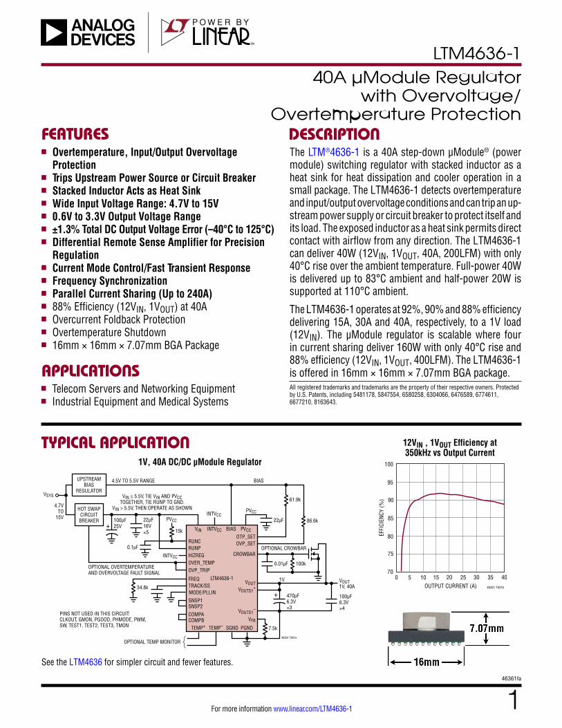
12VIN , 1VOUT Efficiency at 350kHz vs Output Current
OUTPUT CURRENT (A)0
EFFI
CIEN
CY (%
) 90
95
100
15 25
46361 TA01b
85
80
5 10 20 30 4035
75
70
See the LTM4636 for simpler circuit and fewer features.
TEMP+ TEMP– SGND
VIN
1V34.8k
22µF
0.1µF
22µF16V×5
4.7VTO
15V
VSYS
4.5V TO 5.5V RANGE
100µF25V
INTVCC
PVCC
VIN ≤ 5.5V, TIE VIN AND PVCCTOGETHER, TIE RUNP TO GND.
VIN > 5.5V, THEN OPERATE AS SHOWN
OPTIONAL TEMP MONITOR
INTVCC
INTVCCPVCC
LTM4636-1
PVCC
PGND
VOUTS1+
VOUT
OTP_SETOVP_SET
CROWBAROPTIONAL CROWBAR
VOUTS1–
VFB
BIAS
BIAS
+
470µF6.3V×3
+
7.5k
100µF6.3V×4
VOUT1V, 40A
46361 TA01a
PINS NOT USED IN THIS CIRCUIT:CLKOUT, GMON, PGOOD, PHMODE, PWM, SW, TEST1, TEST2, TEST3, TMON
COMPACOMPB
SNSP1SNSP2
MODE/PLLINTRACK/SS
15k
RUNCRUNPHIZREG
OVP_TRIPOVER_TEMP
FREQ
HOT SWAPCIRCUIT
BREAKER
UPSTREAMBIAS
REGULATOR
OPTIONAL OVERTEMPERATUREAND OVERVOLTAGE FAULT SIGNAL
61.9k
86.6k
0.01µF 100k
LTM4636-1
246361fa
For more information www.linear.com/LTM4636-1
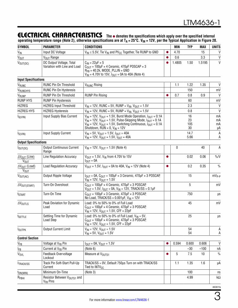
ABSOLUTE MAXIMUM RATINGSVIN, SW, HZBREG, RUNP, OVR_TRIP, OVER TEMP ............................................... –0.3V to 16VVOUT .......................................................... –0.3V to 3.5VPGOOD, RUNC, TMON, PVCC, MODE/PLLIN, PHMODE, FREQ, TRACK/SS, TEST1, TEST2, VOUTS1
–, VOUTS1+, SNSP1, SNSP2, TEST3,
OVP_SET, CROWBAR ....................–0.3V to INTVCC (5V)VFB, COMPA, COMPB (Note 6) .................. –0.3V to 2.7VBIAS ............................................................. –0.3V to 6V
(Note 1)
ORDER INFORMATIONLEAD FREE FINISH TRAY PART MARKING* PACKAGE DESCRIPTION TEMPERATURE RANGE
LTM4636-1EY#PBF LTM4636-1EY#PBF LTM4636-1 144-Lead (16mm × 16mm × 7.07mm) BGA –40°C to 125°C
LTM4636-1IY#PBF LTM4636-1IY#PBF LTM4636-1 144-Lead (16mm × 16mm × 7.07mm) BGA –40°C to 125°C
Consult LTC Marketing for parts specified with wider operating temperature ranges. *The temperature grade is identified by a label on the shipping container.For more information on lead free part marking, go to: http://www.linear.com/leadfree/ This product is only offered in trays. For more information go to: http://www.linear.com/packaging/
PIN CONFIGURATION
1
M
L
K
J
H
G
F
E
D
C
B
A
TOP VIEW
BGA PACKAGE 144-LEAD (16mm × 16mm × 7.07mm)
VOUT
GND
GND
GND
GND
SWVIN
2 3 4 5 6 7 8 9 10 11 12
PGOODRUNC
SNSP2SNSP1
COMPB
TEST2 CROWBAROVP_TRIPOVER_TEMP
OTP_SET
INTVCC
TEMP–
OVP_SET
TEMP+CLKOUT
SGND
VFB
VOUTS1+
HIZREG
TRACK/SS
COMPA
VOUTS1–
FREQ
PWMTEST3
MODE/PLLIN
TEST1 TMON
BIAS
GMON
PHMODERUNPPVCC
TJMAX = 125°C, JA = 7.5°C/W, JCbottom = 3°C/W, JCtop = 15°C/W, JBA = 12°C/W
JA = DERIVED FROM 95mm × 76mm PCB WITH 6 LAYERS, WEIGHT = 3.95g VALUES DETERMINED PER JESD51-12
Note: JA = ( JCbottom + JBA)|| JCtop; JBA is Board to Ambient
PVCC Additional Output Current ................ 0mA to 50mATEMP+, TEMP– .......................................... –0.3V to 0.8VINTVCC Peak Output Current (Note 6) ....................20mAInternal Operating Temperature Range (Note 2) .................................................. –40°C to 125°CStorage Temperature Range .................. –55°C to 125°CReflow (Peak Body) Temperature .......................... 250°C
Note: PWM, CLKOUT, and GMON are outputs only.
http://www.linear.com/product/LTM4636-1#orderinfo
LTM4636-1
346361fa
For more information www.linear.com/LTM4636-1
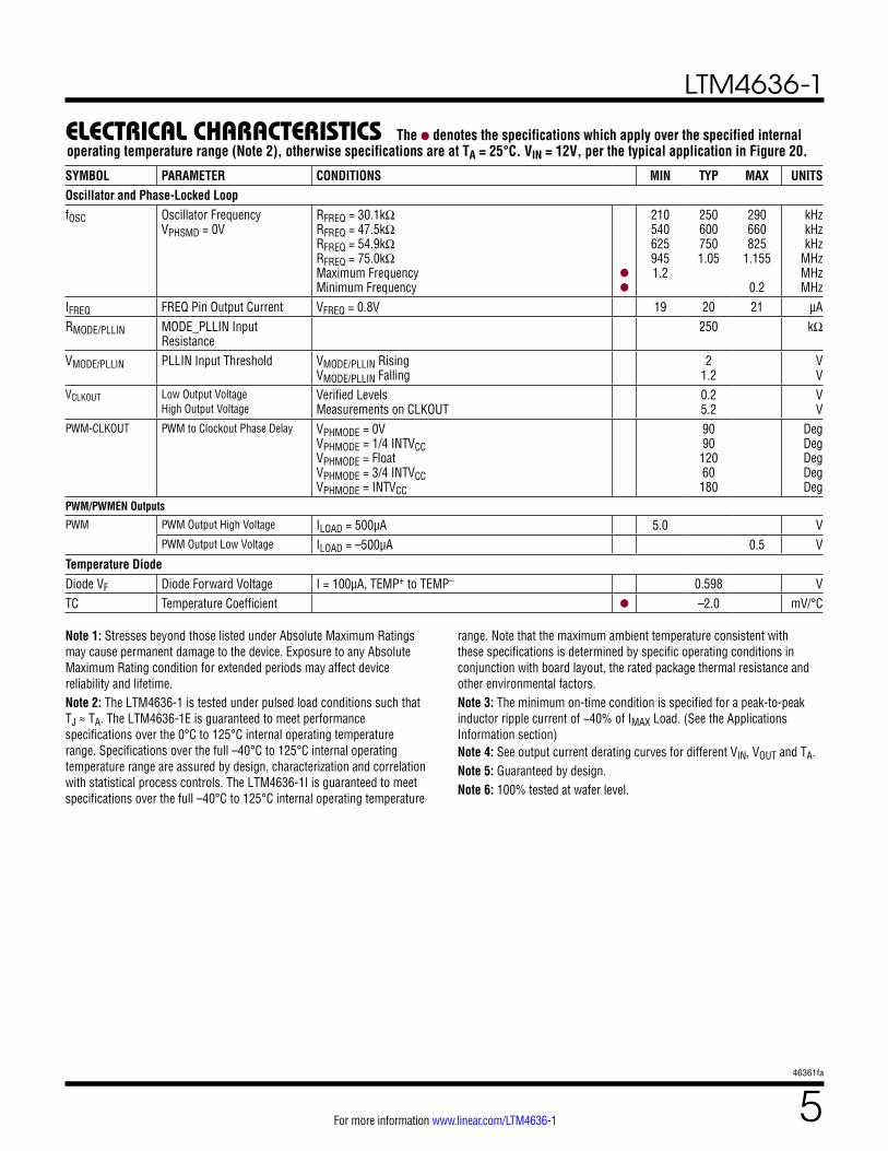
ELECTRICAL CHARACTERISTICS The l denotes the specifications which apply over the specified internal operating temperature range (Note 2), otherwise specifications are at TA = 25°C. VIN = 12V, per the Typical Application in Figure 20.
SYMBOL PARAMETER CONDITIONS MIN TYP MAX UNITSVIN Input DC Voltage VIN ≤ 5.5V, Tie VIN and PVCC Together, Tie RUNP to GND l 4.70 15 VVOUT VOUT Range l 0.6 3.3 VVOUT(DC) DC Output Voltage, Total
Variation with Line and LoadCIN = 22µF × 5 COUT = 100µF × 4 Ceramic, 470µF POSCAP × 3 RFB = 40.2k, MODE_PLLIN = GND VIN = 4.70V to 15V, IOUT = 0A to 40A (Note 4)
l 1.4805 1.50 1.5195 V
Input SpecificationsVRUNC RUNC Pin On Threshold VRUNC Rising 1.1 1.22 1.35 VVRUNCHYS RUNC Pin On Hysteresis 150 mVVRUNP RUNP Pin On Threshold RUNP Pin Rising l 0.7 0.8 0.9 VRUNP HYS RUNP Pin Hysteresis 60 mVHIZREG HIZREG Input Threshold VIN = 12V, RUNC = 5V, RUNP = VIN, VOUT = 1.5V 2.3 VHIZREG HYS HIZREG Hysteresis VIN = 12V, RUNC = 5V, RUNP = VIN, VOUT = 1.5V 0.8 VIQ(VIN) Input Supply Bias Current VIN = 12V, VOUT = 1.5V, Burst Mode Operation, IOUT = 0.1A
VIN = 12V, VOUT = 1.5V, Pulse-Skipping Mode, IOUT = 0.1A VIN = 12V, VOUT = 1.5V, Switching Continuous, IOUT = 0.1A Shutdown, RUN = 0, VIN = 12V
16 23
105 30
mA mA mA µA
IS(VIN) Input Supply Current VIN = 5V, VOUT = 1.5V, IOUT = 40A VIN = 12V, VOUT = 1.5V, IOUT = 40A
14.7 5.66
A A
Output SpecificationsIOUT(DC) Output Continuous Current
Range VIN = 12V, VOUT = 1.5V (Note 4) 0 40 A
∆VOUT (Line) VOUT
Line Regulation Accuracy VOUT = 1.5V, VIN from 4.70V to 15V IOUT = 0A
l 0.02 0.06 %/V
∆VOUT (Load) VOUT
Load Regulation Accuracy VOUT = 1.5V, IOUT = 0A to 40A, VIN = 12V (Note 4) l 0.2 0.35 %
VOUT(AC) Output Ripple Voltage IOUT = 0A, COUT = 100µF × 3 Ceramic, 470µF × 3 POSCAP, VIN = 12V, VOUT = 1.5V
15 mVP-P
∆VOUT(START) Turn-On Overshoot COUT = 100µF × 4 Ceramic, 470µF × 3 POSCAP, VOUT = 1.5V, IOUT = 0A, VIN = 12V, TRACK/SS = 0.1µF
5 mV
tSTART Turn-On Time COUT = 100µF × 3 Ceramic, 470µF × 3 POSCAP, No Load, TRACK/SS = 0.001µF, VIN = 12V
750 µs
∆VOUTLS Peak Deviation for Dynamic Load
Load: 0% to 50% to 0% of Full Load COUT = 100µF × 4 Ceramic, 470µF × 3 POSCAP, VIN = 12V, VOUT = 1.5V, CFF = 22pF
45 mV
tSETTLE Settling Time for Dynamic Load Step
Load: 0% to 50% to 0% of Full Load, VIN = 5V, COUT = 100µF × 4 Ceramic, 470µF × 3 POSCAP, VIN = 12V, VOUT = 1.5V, CFF = 22pF
25 µs
IOUTPK Output Current Limit VIN = 12V, VOUT = 1.5V VIN = 5V, VOUT = 1.5V
54 54
A A
Control SectionVFB Voltage at VFB Pin IOUT = 0A, VOUT = 1.5V l 0.594 0.600 0.606 VIFB Current at VFB Pin (Note 6) –30 –100 nAVOVL Feedback Overvoltage
LockoutMeasure at VOUTS1 l 5 7.5 10 %
ITRACK/SS Track Pin Soft-Start Pull-Up Current
TRACK/SS = 0V, Default 750µs Turn on with TRACK/SS Tied to INTVCC
1.1 1.35 1.6 µA
tON(MIN) Minimum On-Time (Note 3) 100 nsRFBHI Resistor Between VOUTS1 and
VFB Pins4.99 kΩ
LTM4636-1
446361fa
For more information www.linear.com/LTM4636-1
SYMBOL PARAMETER CONDITIONS MIN TYP MAX UNITSRemote Sense AmplifierAV(VFB) VFB Differential Gain (Note 6) 1 V/VGBP VFB Path Gain Bandwidth Product (Note 5) 4 MHzGeneral Control or Monitor PinsOVP ∆t OVP to OVP_TRIP OVP Response Time 500 nsCrowbar ∆t OVP to CROWBAR OVP Response Time to CROWBAR 500 nsOVP Delay OVP to OVER_TEMP OVP_TEMP to OVP_TEMP Response Time 8 µsOVP_Trip Sink OVP_TRIP Sink Current VCE ≤ 0.4V 15 mAOTP_Trip Sink OVER_TEMP Sink Current VCE ≤ 0.4V 15 mACrowbar Source CROWBAR Source Current VCROWBAR ≥ 3.0V 15 mAOTP_SET Overtemperature Set Register 24.9 kΩOVP_SET Overvoltage Set Register 24.9 kΩITMON Temperature Monitor Current, TJ = 25°C Into 24.9kΩ
Temperature Monitor Current, TJ = 150°C Into 24.9kΩ38 40.3
5844 µA
µAITMON(SLOPE) Temperature Monitor Current Slope, RTMON = 24.9kΩ 0.144 µA/°CVPGOOD PGOOD Trip Level VFB With Respect to Set Output
VFB Ramping Negative VFB Ramping Positive
–7.5 7.5
% %
VPGL PGOOD Voltage Low IPGOOD = 2mA 0.2 0.4 VtPGOOD VPGOOD High-to-Low Delay 65 µsIPGOOD(OFF) PGOOD Leakage Current VPGOOD = 5V –2 2 µAVPG1(HYST) PGOOD Trip Level Hysteresis 2.5 %INTVCC Linear RegulatorVINTVCC Internal VCC Voltage Source 6V < VIN < 15V 5.3 5.5 5.7 VVINTVCC Load Reg INTVCC Load Regulation ICC = 0mA to 10mA 0.5 %UVLO HYS Controller UVLO Hysteresis (Note 6) 0.5 VPVCC(UVLO) Drivers and Power MOSFETs
UVLOPVCC Rising 3.5 3.8 4.1 V
PVCC(HYS) PVCC UVLO Hysteresis 0.45 VPVCC Power Stage Bias 12V Input, PVCC Load = 50mA 5.0 VBIAS External Bias for OTP and
OVP FunctionRange Operating 4 5.0 5.5 V
ELECTRICAL CHARACTERISTICS The l denotes the specifications which apply over the specified internal operating temperature range (Note 2), otherwise specifications are at TA = 25°C. VIN = 12V, per the typical application in Figure 20.
LTM4636-1
546361fa
For more information www.linear.com/LTM4636-1
ELECTRICAL CHARACTERISTICS The l denotes the specifications which apply over the specified internal operating temperature range (Note 2), otherwise specifications are at TA = 25°C. VIN = 12V, per the typical application in Figure 20.
Note 1: Stresses beyond those listed under Absolute Maximum Ratings may cause permanent damage to the device. Exposure to any Absolute Maximum Rating condition for extended periods may affect device reliability and lifetime.Note 2: The LTM4636-1 is tested under pulsed load conditions such that TJ ≈ TA. The LTM4636-1E is guaranteed to meet performance specifications over the 0°C to 125°C internal operating temperature range. Specifications over the full –40°C to 125°C internal operating temperature range are assured by design, characterization and correlation with statistical process controls. The LTM4636-1I is guaranteed to meet specifications over the full –40°C to 125°C internal operating temperature
range. Note that the maximum ambient temperature consistent with these specifications is determined by specific operating conditions in conjunction with board layout, the rated package thermal resistance and other environmental factors.Note 3: The minimum on-time condition is specified for a peak-to-peak inductor ripple current of ~40% of IMAX Load. (See the Applications Information section)Note 4: See output current derating curves for different VIN, VOUT and TA.Note 5: Guaranteed by design.Note 6: 100% tested at wafer level.
SYMBOL PARAMETER CONDITIONS MIN TYP MAX UNITSOscillator and Phase-Locked LoopfOSC Oscillator Frequency
VPHSMD = 0VRFREQ = 30.1kΩ RFREQ = 47.5kΩ RFREQ = 54.9kΩ RFREQ = 75.0kΩ Maximum Frequency Minimum Frequency
l
l
210 540 625 945 1.2
250 600 750 1.05
290 660 825
1.155
0.2
kHz kHz kHz
MHz MHz MHz
IFREQ FREQ Pin Output Current VFREQ = 0.8V 19 20 21 µARMODE/PLLIN MODE_PLLIN Input
Resistance250 kΩ
VMODE/PLLIN PLLIN Input Threshold VMODE/PLLIN Rising VMODE/PLLIN Falling
2 1.2
V V
VCLKOUT Low Output Voltage High Output Voltage
Verified Levels Measurements on CLKOUT
0.2 5.2
V V
PWM-CLKOUT PWM to Clockout Phase Delay VPHMODE = 0V VPHMODE = 1/4 INTVCC VPHMODE = Float VPHMODE = 3/4 INTVCC VPHMODE = INTVCC
90 90
120 60
180
Deg Deg Deg Deg Deg
PWM/PWMEN Outputs
PWM PWM Output High Voltage ILOAD = 500µA 5.0 VPWM Output Low Voltage ILOAD = –500µA 0.5 V
Temperature DiodeDiode VF Diode Forward Voltage I = 100µA, TEMP+ to TEMP– 0.598 VTC Temperature Coefficient l –2.0 mV/°C
LTM4636-1
646361fa
For more information www.linear.com/LTM4636-1
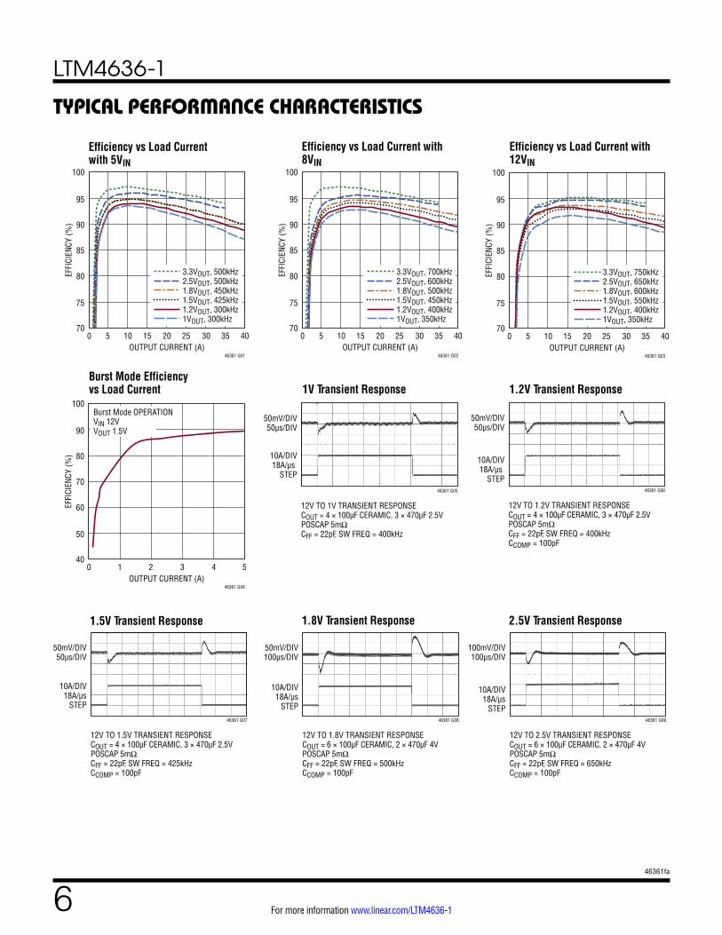
TYPICAL PERFORMANCE CHARACTERISTICS
2.5V Transient Response1.5V Transient Response 1.8V Transient Response
12V TO 1.5V TRANSIENT RESPONSECOUT = 4 × 100µF CERAMIC, 3 × 470µF 2.5V POSCAP 5mΩCFF = 22pF, SW FREQ = 425kHzCCOMP = 100pF
10A/DIV18A/µs
STEP
50mV/DIV50µs/DIV
46361 G07
12V TO 1.8V TRANSIENT RESPONSECOUT = 6 × 100µF CERAMIC, 2 × 470µF 4V POSCAP 5mΩCFF = 22pF, SW FREQ = 500kHzCCOMP = 100pF
10A/DIV18A/µs
STEP
50mV/DIV100µs/DIV
46361 G08
12V TO 2.5V TRANSIENT RESPONSECOUT = 6 × 100µF CERAMIC, 2 × 470µF 4V POSCAP 5mΩCFF = 22pF, SW FREQ = 650kHzCCOMP = 100pF
10A/DIV18A/µs
STEP
100mV/DIV100µs/DIV
46361 G09
Burst Mode Efficiency vs Load Current 1V Transient Response 1.2V Transient Response
Efficiency vs Load Current with 5VIN
Efficiency vs Load Current with 8VIN
Efficiency vs Load Current with 12VIN
OUTPUT CURRENT (A)0
EFFI
CIEN
CY (%
)
100
90
80
95
85
75
702515 35
46361 G01
4020105 30
3.3VOUT, 500kHz2.5VOUT, 500kHz1.8VOUT, 450kHz1.5VOUT, 425kHz1.2VOUT, 300kHz1VOUT, 300kHz
OUTPUT CURRENT (A)0
EFFI
CIEN
CY (%
)
100
90
80
95
85
75
702515 35
46361 G02
4020105 30
3.3VOUT, 700kHz2.5VOUT, 600kHz1.8VOUT, 500kHz1.5VOUT, 450kHz1.2VOUT, 400kHz1VOUT, 350kHz
OUTPUT CURRENT (A)0
EFFI
CIEN
CY (%
)
100
90
80
95
85
75
702515 35
46361 G03
4020105 30
3.3VOUT, 750kHz2.5VOUT, 650kHz1.8VOUT, 600kHz1.5VOUT, 550kHz1.2VOUT, 400kHz1VOUT, 350kHz
OUTPUT CURRENT (A)0
EFFI
CIEN
CY (%
)
100
80
60
90
70
50
4032 4
46361 G04
51
Burst Mode OPERATIONVIN 12VVOUT 1.5V
12V TO 1V TRANSIENT RESPONSECOUT = 4 × 100µF CERAMIC, 3 × 470µF 2.5V POSCAP 5mΩCFF = 22pF, SW FREQ = 400kHz
10A/DIV18A/µs
STEP
50mV/DIV50µs/DIV
46361 G05
12V TO 1.2V TRANSIENT RESPONSECOUT = 4 × 100µF CERAMIC, 3 × 470µF 2.5V POSCAP 5mΩCFF = 22pF, SW FREQ = 400kHzCCOMP = 100pF
10A/DIV18A/µs
STEP
50mV/DIV50µs/DIV
46361 G06
LTM4636-1
746361fa
For more information www.linear.com/LTM4636-1
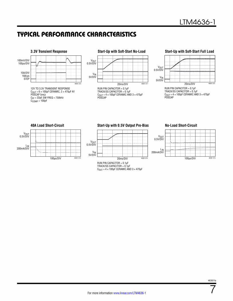
TYPICAL PERFORMANCE CHARACTERISTICS
3.3V Transient Response
40A Load Short-Circuit
Start-Up with Soft-Start No-Load
Start-Up with 0.5V Output Pre-Bias
Start-Up with Soft-Start Full Load
No-Load Short-Circuit
RUN PIN CAPACITOR = 0.1µFTRACK/SS CAPACITOR = 0.1µFCOUT = 4 × 100µF CERAMIC AND 3 × 470µF POSCAP
20ms/DIV
VIN5V/DIV
VOUT0.5V/DIV
46361 G11
RUN PIN CAPACITOR = 0.1µFTRACK/SS CAPACITOR = 0.1µFCOUT = 4 × 100µF CERAMIC AND 3 × 470µF POSCAP
20ms/DIV
VIN5V/DIV
VOUT0.5V/DIV
46361 G12
100µs/DIV
LIN200mA/DIV
VOUT0.5V/DIV
46361 G13
RUN PIN CAPACITOR = 0.1µFTRACK/SS CAPACITOR = 0.1µFCOUT = 4 × 100µF CERAMIC AND 3 × 470µF
20ms/DIV
VIN5V/DIV
VOUT0.5V/DIV
46361 G14 100µs/DIV
LIN200mA/DIV
VOUT0.5V/DIV
46361 G15
12V TO 3.3V TRANSIENT RESPONSECOUT = 6 × 100µF CERAMIC, 2 × 470µF 4V POSCAP 5mΩCFF = 22pF, SW FREQ = 750kHzCCOMP = 100pF
10A/DIV18A/µs
STEP
100mV/DIV100µs/DIV
46361 G10
LTM4636-1
846361fa
For more information www.linear.com/LTM4636-1
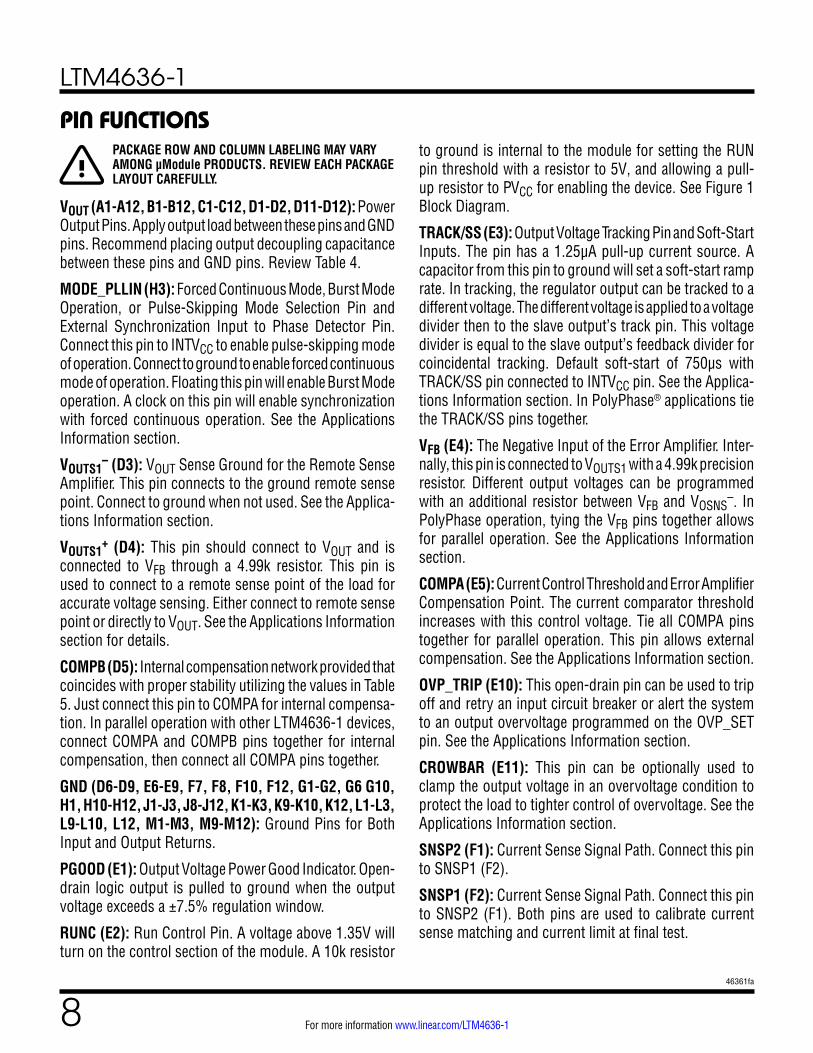
PIN FUNCTIONS
VOUT (A1-A12, B1-B12, C1-C12, D1-D2, D11-D12): Power Output Pins. Apply output load between these pins and GND pins. Recommend placing output decoupling capacitance between these pins and GND pins. Review Table 4.
MODE_PLLIN (H3): Forced Continuous Mode, Burst Mode Operation, or Pulse-Skipping Mode Selection Pin and External Synchronization Input to Phase Detector Pin. Connect this pin to INTVCC to enable pulse-skipping mode of operation. Connect to ground to enable forced continuous mode of operation. Floating this pin will enable Burst Mode operation. A clock on this pin will enable synchronization with forced continuous operation. See the Applications Information section.
VOUTS1– (D3): VOUT Sense Ground for the Remote Sense
Amplifier. This pin connects to the ground remote sense point. Connect to ground when not used. See the Applica-tions Information section.
VOUTS1+ (D4): This pin should connect to VOUT and is
connected to VFB through a 4.99k resistor. This pin is used to connect to a remote sense point of the load for accurate voltage sensing. Either connect to remote sense point or directly to VOUT. See the Applications Information section for details.
COMPB (D5): Internal compensation network provided that coincides with proper stability utilizing the values in Table 5. Just connect this pin to COMPA for internal compensa-tion. In parallel operation with other LTM4636-1 devices, connect COMPA and COMPB pins together for internal compensation, then connect all COMPA pins together.
GND (D6-D9, E6-E9, F7, F8, F10, F12, G1-G2, G6 G10, H1, H10-H12, J1-J3, J8-J12, K1-K3, K9-K10, K12, L1-L3, L9-L10, L12, M1-M3, M9-M12): Ground Pins for Both Input and Output Returns.
PGOOD (E1): Output Voltage Power Good Indicator. Open-drain logic output is pulled to ground when the output voltage exceeds a ±7.5% regulation window.
RUNC (E2): Run Control Pin. A voltage above 1.35V will turn on the control section of the module. A 10k resistor
to ground is internal to the module for setting the RUN pin threshold with a resistor to 5V, and allowing a pull-up resistor to PVCC for enabling the device. See Figure 1 Block Diagram.
TRACK/SS (E3): Output Voltage Tracking Pin and Soft-Start Inputs. The pin has a 1.25µA pull-up current source. A capacitor from this pin to ground will set a soft-start ramp rate. In tracking, the regulator output can be tracked to a different voltage. The different voltage is applied to a voltage divider then to the slave output’s track pin. This voltage divider is equal to the slave output’s feedback divider for coincidental tracking. Default soft-start of 750µs with TRACK/SS pin connected to INTVCC pin. See the Applica-tions Information section. In PolyPhase® applications tie the TRACK/SS pins together.
VFB (E4): The Negative Input of the Error Amplifier. Inter-nally, this pin is connected to VOUTS1 with a 4.99k precision resistor. Different output voltages can be programmed with an additional resistor between VFB and VOSNS
–. In PolyPhase operation, tying the VFB pins together allows for parallel operation. See the Applications Information section.
COMPA (E5): Current Control Threshold and Error Amplifier Compensation Point. The current comparator threshold increases with this control voltage. Tie all COMPA pins together for parallel operation. This pin allows external compensation. See the Applications Information section.
OVP_TRIP (E10): This open-drain pin can be used to trip off and retry an input circuit breaker or alert the system to an output overvoltage programmed on the OVP_SET pin. See the Applications Information section.
CROWBAR (E11): This pin can be optionally used to clamp the output voltage in an overvoltage condition to protect the load to tighter control of overvoltage. See the Applications Information section.
SNSP2 (F1): Current Sense Signal Path. Connect this pin to SNSP1 (F2).
SNSP1 (F2): Current Sense Signal Path. Connect this pin to SNSP2 (F1). Both pins are used to calibrate current sense matching and current limit at final test.
PACKAGE ROW AND COLUMN LABELING MAY VARY AMONG µModule PRODUCTS. REVIEW EACH PACKAGE LAYOUT CAREFULLY.
LTM4636-1
946361fa
For more information www.linear.com/LTM4636-1
PIN FUNCTIONSHIZREG (F3): When this pin is pulled low the power stage is disabled into high impedance. Tie this pin to VIN or INTVCC for normal operation.
OVER_TEMP (D10): This overtemperature protection is programmable with an internal monitor that is referenced to the TMON pin and the OTP_SET pin. The OVER_TEMP pin can be used to alert the system if the module regulator overheats, and this signal can be used to trip off and retry an electronic circuit breaker in a fault condition. The pin is an open collector that pulls active low in response to OVER_TEMP. The OVER_TEMP pin can be left floating if not used. See the Applications Information section for details.
SGND (F4, G4): Signal Ground Pin. Return ground path for all analog and low power circuitry. Tie a single connection to the output capacitor GND in the application. See layout guidelines in Figure 18.
INTVCC (F6): Internal 5.5V LDO for Driving the Control Circuitry in the LTM4636-1. INTVCC is controlled and enabled when RUNC is activated high.
FREQ (G5): A resistor can be applied from this pin to ground to set the operating frequency. This pin sources 20µA. See the Applications Information section.
PHMODE (G7): This pin can be voltage programmed to change the phase relationship of the CLKOUT pin with refer-ence to the internal clock or an input synchronized clock. The INTVCC (5.5V) output can be voltage divided down to the PHASMD pin to set the particular phase. The Electri-cal Characteristics show the different settings to select a particular phase. See the Applications Information section.
RUNP (G8): This pin enables the PVCC supply. This pin can be connected to VIN, or tie to ground when connecting PVCC to VIN ≤ 5.5V. RUNP needs to sequence up before RUNC. A 15k resistor from PVCC to RUNC with a 0.1µF capacitor will provide enough delay. In parallel operation with multiple LTM4636-1s, the resistor can be reduced in value by N times and the 0.1µF can be increased N times. See Applications Information section. RUNP can be used to set the minimum UVLO with a voltage divider. See Figure 1.
PVCC (F9): 5V Power Output and Power for Internal Power MOSFET Drivers. The regulator can power 50mA of external sourcing for additional use. Place a 22µF ceramic filter capacitor on this pin to ground. When VIN < 5.5V, tie VIN
and PVCC together. Then tie RUNP to GND. If VIN > 5.5V then operate PVCC regulator as normal. See the Typical Application examples.
OVP_SET (E12): This pin is used to set the output overvolt-age trip point. This pin has a 24.9kΩ resistor on it to ground. See the Applications Information section. Float is not used.
BIAS (G9): This pin is used to power the OTP and OVP circuitry independently of the main power feed. See the Applications Information section.
TEMP+ (G12): Temperature Monitor. An internal diode connected NPN transistor. See the Applications Informa-tion section.
OTP_SET (F11): This pin is used to set the overtemperature set point. The pin has a 24.9k resistor on it to ground. See Applications Information section. Float if not used.
TEMP– (G11): Low Side of the Internal Temperature Monitor.
CLKOUT (G3): Clock out signal that can be phase selected to the main internal clock or synchronized clock using the PHASMD pin. CLKOUT can be used for multiphase applications. See the Applications Information section.
TEST1 (H4), TEST2 (F5), TEST3 (H2), GMON (H9):These are test pins used in the final production test of the part. Leave floating.
VIN (H5-H6, J4-J7, K4-K8, L4-L8, M4-M8): Power Input Pins. Apply input voltage between these pins and GND pins. Recommend placing input decoupling capacitance directly between VIN and GND pins.
PWM (H7): PWM output that drives the power stage. Primar-ily used for test, but can be monitored in debug or testing.
TMON (H8): Temperature Monitor Pin. Internal temperature monitor, varies from 1.0V at 25°C to 1.44V at 150°C, disables power stage at >150°C. The OTP_Trip signal is set to trip off at a value lower than 150°C. If the temperature moni-tor feature is not desired, then tie the TMON pin to GND.
SW (L11, K11): These are pin connections to the internal switch node for test evaluation and monitoring. An R-C snubber can be placed from the switch pins to GND to eliminate any high frequency ringing. See the Applications Information section.
LTM4636-1
1046361fa
For more information www.linear.com/LTM4636-1
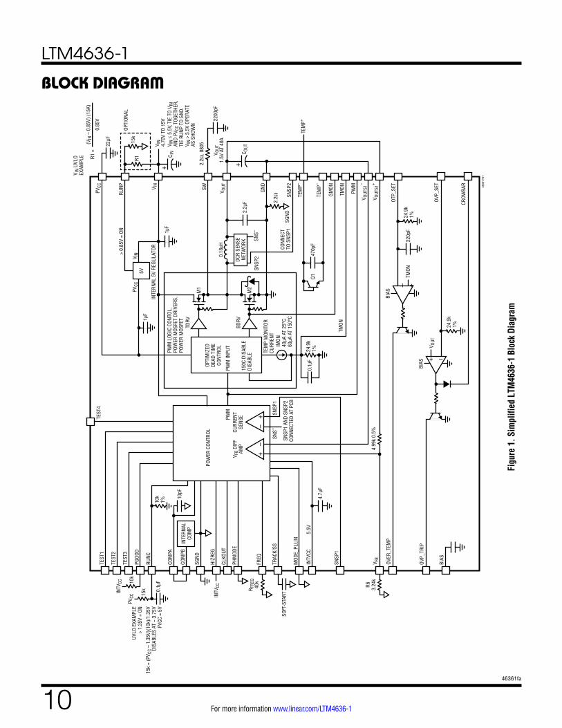
BLOCK DIAGRAM
Figu
re 1
. Sim
plifi
ed L
TM46
36-1
Blo
ck D
iagr
am
PGOO
D
+
TDRV
PWM
INPU
T
150C
DIS
ABLE
DISA
BLE TE
MP
MON
ITOR
CURR
ENT
IMON
40µA
AT
25°C
60µA
AT
150°
C
PWM
LOG
IC C
ONTO
L,PO
WER
MOS
FET
DRIV
ERS,
POW
ER M
OSFE
T
M1
0.18
µH
SNSP
2SN
S–
BDRV
M2
24.9
k1%
4.99
k 0.
5%
0.1µ
F
10pF
0.1µ
F
SOFT
-STA
RT
10k
1%
UVLO
EXA
MPL
E>
1.35
V =
ON
15k
= (P
V CC
– 1.
35V)
(10k
)/1.3
5VDI
SABL
ES A
T ~
3.75
VPV
CC =
5V
15k
10k
INTV
CC
PVCC
SNSP
1
SNSP
1 AN
D SN
SP2
CONN
ECTE
D AT
PCB
SNS–
470p
FQ1
1µF
22µF
OPTI
ONAL
V IN
PVCC
> 0.
85V
= ON
INTE
RNAL
5V
REGU
LATO
R
2.2Ω
2.2µ
F
2.2Ω
, 080
5
SGND
SNSP
2CO
NNEC
TTO
SNS
P1
TEM
P–
GMON
TMON
PWM
V OUT
S1–
TEM
P–TE
MP+
GND
V OUT
V OUT
1.5V
AT
40A
SWV IN
V IN
4.70
V TO
15V
V IN
≤ 5.
5V, T
IE T
O V I
NAN
D PV
CC T
OGET
HER,
TIE
RUNP
TO
GND.
V IN
> 5.
5V O
PERA
TE
AS S
HOW
N
V IN
UVLO
EXAM
PLE C I
N
RUNP
R1
PVCC
OPTI
MIZ
EDDE
AD T
IME
CONT
ROL
DCR
SENS
ENE
TWOR
K
5V
V OUT
S1+
+–
V FB
DIFF
AMP
CURR
ENT
SENS
EPWM
POW
ER C
ONTR
OL
FREQ
TRAC
K/SS
V FB
R6 3.24
k
MOD
E_PL
LIN
INTV
CC5.
5V
SNSP
1
PHM
ODE
HIZR
EGIN
TVCC
CLKO
UT
SGND
COM
PB
COM
PA
RUNC
TEST
3
TEST
2
TEST
1TE
ST4
R FRE
Q40
k
TMON
BIAS
OTP_
SET
4636
1 F0
1
OVER
_TEM
P
+–
+C O
UT
4.7µ
F
INTE
RNAL
COM
P
1µF
2200
pF
15k
R1 =
(V
IN –
0.8
5V) (
15K)
0.85
V
24.9
k1%
– +
220p
F
BIAS
OVP_
SET
OVP_
TRIP
BIAS
24.9
k1%
V OUT
+ –
CROW
BAR
TMON
LTM4636-1
1146361fa
For more information www.linear.com/LTM4636-1
DECOUPLING REQUIREMENTSSYMBOL PARAMETER CONDITIONS MIN TYP MAX UNITS
CIN External Input Capacitor Requirement (VIN = 4.70V to 16V, VOUT = 1.5V)
IOUT = 40A, 6 × 22µF Ceramic X7R Capacitors (See Table 4)
100 µF
COUT External Output Capacitor Requirement (VIN = 4.70V to 16V, VOUT = 1.5V)
IOUT = 40A (See Table 4) 1000 µF
TA = 25°C. Use Figure 1 configuration.
Power Module Description
The LTM4636-1 is a high efficiency regulator that can provide a 40A output with few external input and output capacitors. This module provides precisely regulated output voltages programmable via external resistors from 0.6V DC to 3.3V DC over a 4.70V to 15V input range. The Typical Application schematic with protection is shown in Figure 20.
The LTM4636-1 has an integrated constant-frequency current mode regulator, power MOSFETs, 0.18µH induc-tor, protection circuitry, 5V regulator and other supporting discrete components. The switching frequency range is from 250kHz to 770kHz, and the typical operating frequency is 400kHz. For switching noise-sensitive applications, it can be externally synchronized from 250kHz to 800kHz, subject to minimum on-time limitations and limiting the inductor ripple current to less than 40% of maximum output current.
A single resistor is used to program the frequency. See the Applications Information section.
With current mode control and internal feedback loop compensation, the LTM4636-1 module has sufficient sta-bility margins and good transient performance with a wide range of output capacitors, even with all ceramic output capacitors. An option has been provided for external loop compensation. LTpowerCAD™ can be used to optimize the external compensation option. See the Applications Information section.
Current mode control provides cycle-by-cycle fast current limit in an overcurrent condition. An internal overvoltage monitor feedback pin referred will attempt to protect the output voltage in the event of an overvoltage >10%. The top MOSFET is turned off and the bottom MOSFET is turned on until the output is cleared.
OPERATIONPulling the RUNC pin below 1.1V forces the regulator con-troller into a shutdown state. The TRACK/SS pin is used for programming the output voltage ramp and voltage tracking during start-up. See the Applications Information section.
Optional internal overvoltage protection and overtem-perature functions can be used to protect from power MOSFET failures, input and output overvoltage and over-temperature conditions. These two features can be used to trip off and retry an input circuit breaker in the event of either/or both an overvoltage and overtemperature fault. The OVP_TRIP, OVER_TEMP, TMON, OVP_SET, CROWBAR and OTP_SET pins are all used to support these two features. These features can be implemented along with an input circuit breaker to protect expensive systems boards, processors and FPGA devices from damage. See the Applications Information section.
The LTM4636-1 is internally compensated to be stable over all operating conditions. Table 5 provides a guideline for input and output capacitances for several operating conditions. LTpowerCAD is available for transient and stability analysis. This tool can be used to optimize the regulators loop response.
A remote sense amplifier is provided for accurately sensing output voltages at the load point.
Multiphase operation can be easily employed with the internal clock source or a synchronization clock applied to the MODE/PLLIN input using an external clock source, and connecting the CLKOUT pins. See the Applications Information section. Review Figure 4.
High efficiency at light loads can be accomplished with selectable Burst Mode operation using the MODE_PLLIN pin. These light load features will accommodate battery operation. Efficiency graphs are provided for light load op-eration in the Typical Performance Characteristics section.
LTM4636-1
1246361fa
For more information www.linear.com/LTM4636-1
OPERATIONA TEMP+ and TEMP– pins are provided to allow the internal device temperature to be monitored using an onboard diode connected NPN transistor.
High efficiency at light loads can be accomplished with selectable Burst Mode operation using the MODE_PLLIN pin. These light load features will accommodate battery operation. Efficiency graphs are provided for light load op-eration in the Typical Performance Characteristics section.
APPLICATIONS INFORMATIONThe typical LTM4636-1 application circuit is shown in Figure 20. External component selection is primarily determined by the maximum load current and output voltage. Refer to Table 5 for specific external capacitor requirements for particular applications.
VIN to VOUT Step-Down Ratios
There are restrictions in the VIN to VOUT step-down ratio that can be achieved for a given input voltage. The maximum duty cycle is 94% typical at 500kHz operation. The VIN to VOUT minimum dropout is a function of load current and operation at very low input voltage and high duty cycle applications. At very low duty cycles the minimum 100ns on-time must be maintained. See the PLL, Frequency Adjustment and Synchronization section and temperature derating curves.
Output Voltage Programming
The PWM controller has an internal 0.6V ±1% reference voltage. As shown in the Block Diagram, a 4.99k internal feedback resistor connects the VOUTS1 and VFB pins to-gether. When the remote sensing is used, then VOUTS1
+
and VOUTS1– are connected to the remote VOUT and GND
points. If no remote sense the VOUTS1+ connects to VOUT.
The output voltage will default to 0.6V with no feedback resistor. Adding a resistor RFB from VFB to ground programs the output voltage:
VOUT 0.6V •
4.99k R FBR FB
Table 1. VFB Resistor Table vs Various Output VoltagesVOUT (V) 0.6 1.0 1.2 1.5 1.8 2.5 3.3
RFB (k) Open 7.5 4.99 3.24 2.49 1.58 1.1
For parallel operation of N LTM4636-1s, the following equation can be used to solve for RFB:
RFB4.99k / NVOUT0.6V
– 1
Or use VOUTS1 on one channel and connect all feedback pins together utilizing a single feedback resistor.
Tie the VFB pins together for each parallel output. The COMP pins must be tied together also. See the Typical Applications section examples.
Input Capacitors
The LTM4636-1 module should be connected to a low AC-impedance DC source. Additional input capacitors are needed for the RMS input ripple current rating. The ICIN(RMS)equation which follows can be used to calculate the input capacitor requirement. Typically 22µF X7R ceramics are a good choice with RMS ripple current ratings of ~4A each. A 47µF to 100µF surface mount aluminum electrolytic bulk capacitor can be used for more input bulk capacitance. This bulk input capacitor is only needed if the input source impedance is compromised by long inductive leads, traces or not enough source capacitance. If low impedance power planes are used, then this bulk capacitor is not needed.
For a buck converter, the switching duty cycle can be estimated as:
D
VOUTVIN
LTM4636-1
1346361fa
For more information www.linear.com/LTM4636-1
APPLICATIONS INFORMATIONWithout considering the inductor ripple current, for each output the RMS current of the input capacitor can be estimated as:
ICIN(RMS)
IOUT(MAX)
%• D •(1– D)
where % is the estimated efficiency of the power mod-ule. The bulk capacitor can be a switcher-rated aluminum electrolytic capacitor or a Polymer capacitor.
Output Capacitors
The LTM4636-1 is designed for low output voltage ripple noise. The bulk output capacitors defined as COUT are chosen with low enough effective series resistance (ESR) to meet the output voltage ripple and transient require-ments. COUT can be a low ESR tantalum capacitor, low ESR Polymer capacitor or ceramic capacitors. The typi-cal output capacitance range is from 400µF to 1000µF. Additional output filtering may be required by the system designer if further reduction of output ripple or dynamic transient spikes is required. Table 5 shows a matrix of dif-ferent output voltages and output capacitors to minimize the voltage droop and overshoot during a 15A/µs tran-sient. The table optimizes total equivalent ESR and total bulk capacitance to optimize the transient performance. Stability criteria are considered in the Table 5 matrix, and LTpowerCAD is available for stability analysis. Multiphase operation will reduce effective output ripple as a function of the number of phases. Application Note 77 discusses this noise reduction versus output ripple current cancel-lation, but the output capacitance should be considered carefully as a function of stability and transient response. LTpowerCAD can be used to calculate the output ripple reduction as the number of implemented phases increases by N times. External loop compensation can be used for transient response optimization.
Burst Mode Operation
The LTM4636-1 is capable of Burst Mode operation in which the power MOSFETs operate intermittently based on load demand, thus saving quiescent current. For ap-plications where maximizing the efficiency at very light loads is a high priority, Burst Mode operation should be applied. To enable Burst Mode operation, simply float
the MODE_PLLIN pin. During Burst Mode operation, the peak current of the inductor is set to approximately 30% of the maximum peak current value in normal operation even though the voltage at the COMPA pin indicates a lower value. The voltage at the COMPA pin drops when the inductor’s average current is greater than the load requirement. As the COMPA voltage drops below 0.5V, the burst comparator trips, causing the internal sleep line to go high and turn off both power MOSFETs.
In sleep mode, the internal circuitry is partially turned off, reducing the quiescent current. The load current is now being supplied from the output capacitors. When the output voltage drops, causing COMPA to rise, the internal sleep line goes low, and the LTM4636-1 resumes normal operation. The next oscillator cycle will turn on the top power MOSFET and the switching cycle repeats.
Pulse-Skipping Mode Operation
In applications where low output ripple and high effi-ciency at intermediate currents are desired, pulse-skipping mode should be used. Pulse-skipping operation allows the LTM4636-1 to skip cycles at low output loads, thus increasing efficiency by reducing switching loss. Tying the MODE_PLLIN pin to INTVCC enables pulse-skipping operation. With pulse-skipping mode at light load, the internal current comparator may remain tripped for several cycles, thus skipping operation cycles. This mode has lower ripple than Burst Mode operation and maintains a higher frequency operation than Burst Mode operation.
Forced Continuous Operation
In applications where fixed frequency operation is more critical than low current efficiency, and where the lowest output ripple is desired, forced continuous operation should be used. Forced continuous operation can be enabled by tying the MODE_PLLIN pin to ground. In this mode, inductor current is allowed to reverse during low output loads, the COMPA voltage is in control of the current comparator threshold throughout, and the top MOSFET always turns on with each oscillator pulse. During start-up, forced continuous mode is disabled and inductor current is prevented from reversing until the LTM4636-1’s output voltage is in regulation.
LTM4636-1
1446361fa
For more information www.linear.com/LTM4636-1
Multiphase Operation
For outputs that demand more than 40A of load current, multiple LTM4636-1 devices can be paralleled to provide more output current without increasing input and output ripple voltage. The MODE_PLLIN pin allows the LTM4636-1 to be synchronized to an external clock and the internal phase-locked loop allows the LTM4636-1 to lock onto input clock phase as well. The FREQ resistor is selected for normal frequency, then the incoming clock can syn-chronize the device over the specified range.
A multiphase power supply significantly reduces the amount of ripple current in both the input and output ca-pacitors. The RMS input ripple current is reduced by, and the effective ripple frequency is multiplied by, the number of phases used (assuming that the input voltage is greater than the number of phases used times the output voltage). The output ripple amplitude is also reduced by the number of phases used. See Application Note 77.
The LTM4636-1 device is an inherently current mode controlled device, so parallel modules will have good cur-rent sharing. This will balance the thermals in the design.
Tie the COMPA to COMPB and then tie the COMPA pins together, tie VFB pins of each LTM4636-1 together to share the current evenly. Figure 21 shows a schematic of the parallel design. For external compensation and parallel operation only tie COMP A pins together with external compensation.
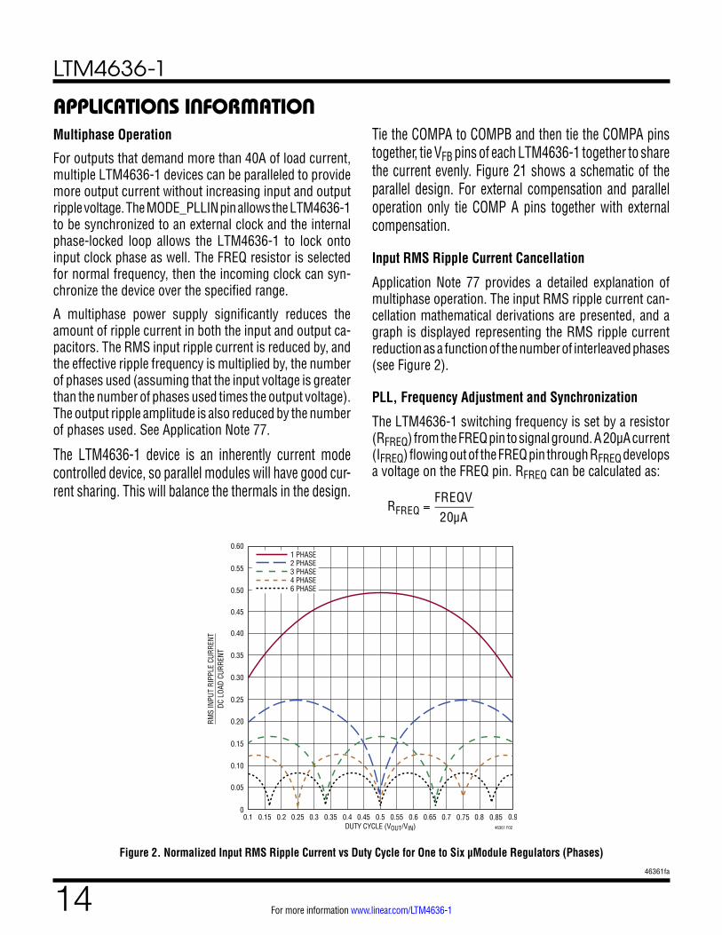
Input RMS Ripple Current Cancellation
Application Note 77 provides a detailed explanation of multiphase operation. The input RMS ripple current can-cellation mathematical derivations are presented, and a graph is displayed representing the RMS ripple current reduction as a function of the number of interleaved phases (see Figure 2).
PLL, Frequency Adjustment and Synchronization
The LTM4636-1 switching frequency is set by a resistor (RFREQ) from the FREQ pin to signal ground. A 20µA current (IFREQ) flowing out of the FREQ pin through RFREQ develops a voltage on the FREQ pin. RFREQ can be calculated as:
RFREQFREQV20µA
APPLICATIONS INFORMATION
Figure 2. Normalized Input RMS Ripple Current vs Duty Cycle for One to Six µModule Regulators (Phases)
0.75 0.846361 F02
0.70.650.60.550.50.450.40.350.30.250.20.150.1 0.85 0.9DUTY CYCLE (VOUT/VIN)
0
DC L
OAD
CURR
ENT
RMS
INPU
T RI
PPLE
CUR
RENT
0.05
0.10
0.15
0.20
0.25
0.30
0.35
0.40
0.45
0.50
0.55
0.601 PHASE2 PHASE3 PHASE4 PHASE6 PHASE
LTM4636-1
1546361fa
For more information www.linear.com/LTM4636-1
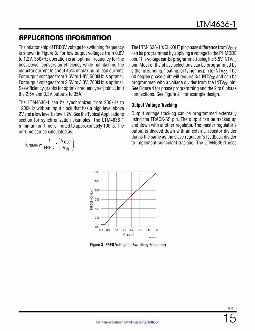
The relationship of FREQV voltage to switching frequency is shown in Figure 3. For low output voltages from 0.6V to 1.2V, 350kHz operation is an optimal frequency for the best power conversion efficiency while maintaining the inductor current to about 45% of maximum load current. For output voltages from 1.5V to 1.8V, 500kHz is optimal. For output voltages from 2.5V to 3.3V, 700kHz is optimal. See efficiency graphs for optimal frequency set point. Limit the 2.5V and 3.3V outputs to 35A.
The LTM4636-1 can be synchronized from 200kHz to 1200kHz with an input clock that has a high level above 2V and a low level below 1.2V. See the Typical Applications section for synchronization examples. The LTM4636-1 minimum on-time is limited to approximately 100ns. The on-time can be calculated as:
tON(MIN)1
FREQ•
VOUTVIN
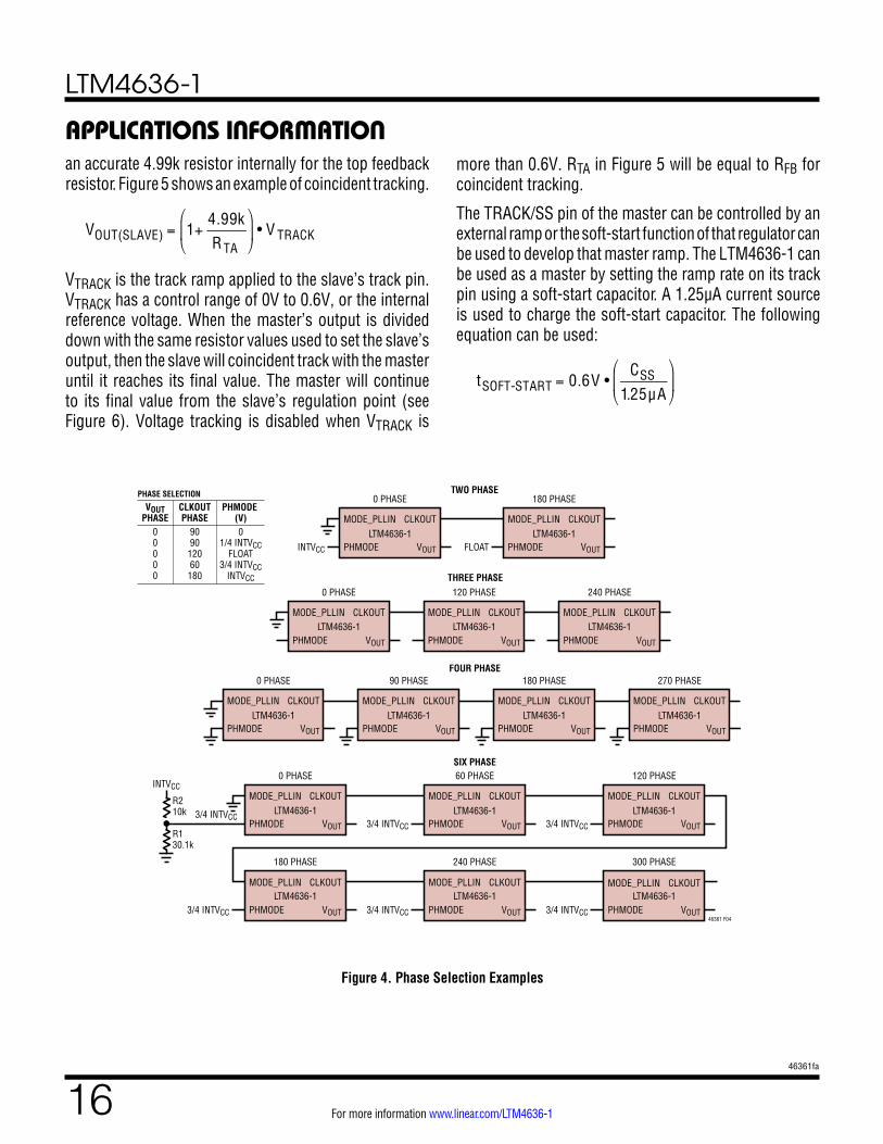
APPLICATIONS INFORMATIONThe LTM4636-1's CLKOUT pin phase difference from VOUTcan be programmed by applying a voltage to the PHMODE pin. This voltage can be programmed using the 5.5V INTVCCpin. Most of the phase selections can be programmed by either grounding, floating, or tying this pin to INTVCC. The 60 degree phase shift will require 3/4 INTVCC and can be programmed with a voltage divider from the INTVCC pin. See Figure 4 for phase programming and the 2 to 6 phase connections. See Figure 21 for example design.
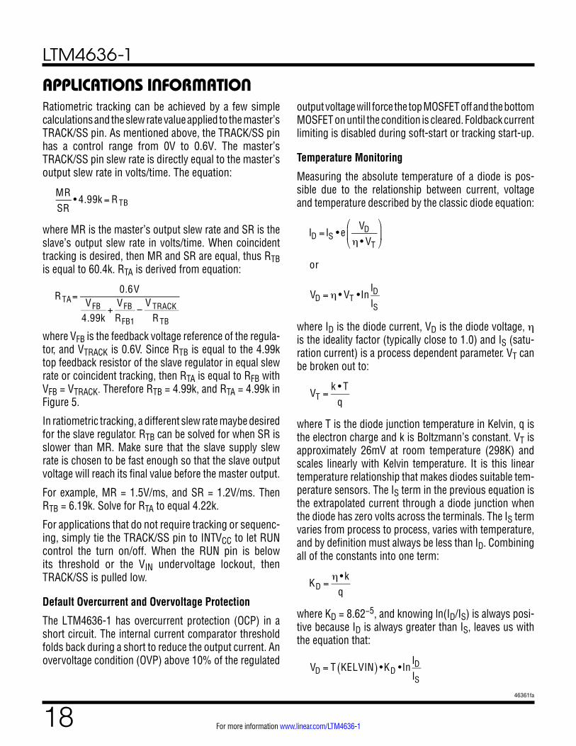
Output Voltage Tracking
Output voltage tracking can be programmed externally using the TRACK/SS pin. The output can be tracked up and down with another regulator. The master regulator’s output is divided down with an external resistor divider that is the same as the slave regulator’s feedback divider to implement coincident tracking. The LTM4636-1 uses
Figure 3. FREQ Voltage to Switching Frequency
VFREQ (V)0.4
FREQ
UENC
Y (k
Hz)
900
1100
1300
1.0 1.4
46361 F03
700
500
0.6 0.8 1.2 1.6 1.8
300
100
LTM4636-1
1646361fa
For more information www.linear.com/LTM4636-1
APPLICATIONS INFORMATIONan accurate 4.99k resistor internally for the top feedback resistor. Figure 5 shows an example of coincident tracking.
VOUT(SLAVE) 1
4.99kR TA
• V TRACK
VTRACK is the track ramp applied to the slave’s track pin. VTRACK has a control range of 0V to 0.6V, or the internal reference voltage. When the master’s output is divided down with the same resistor values used to set the slave’s output, then the slave will coincident track with the master until it reaches its final value. The master will continue to its final value from the slave’s regulation point (see Figure 6). Voltage tracking is disabled when VTRACK is
more than 0.6V. RTA in Figure 5 will be equal to RFB for coincident tracking.
The TRACK/SS pin of the master can be controlled by an external ramp or the soft-start function of that regulator can be used to develop that master ramp. The LTM4636-1 can be used as a master by setting the ramp rate on its track pin using a soft-start capacitor. A 1.25µA current source is used to charge the soft-start capacitor. The following equation can be used:
tSOFT-START 0.6V •
CSS1.25µA
Figure 4. Phase Selection Examples
LTM4636-1
180 PHASE
MODE_PLLIN
PHMODE
CLKOUT
VOUT3/4 INTVCC
LTM4636-1
240 PHASE
MODE_PLLIN
PHMODE
CLKOUT
VOUT3/4 INTVCC
LTM4636-1
300 PHASE
MODE_PLLIN
PHMODE46361 F04
CLKOUT
VOUT3/4 INTVCC
LTM4636-1
0 PHASE
MODE_PLLIN
PHMODE
R210k
R130.1k
CLKOUT
VOUT
LTM4636-1
0 PHASE
MODE_PLLIN
PHMODE
CLKOUT
VOUT
LTM4636-1
90 PHASE
MODE_PLLIN
PHMODE
CLKOUT
VOUT
LTM4636-1
180 PHASE
MODE_PLLIN
PHMODE
CLKOUT
VOUT
LTM4636-1
270 PHASE
MODE_PLLIN
PHMODE
CLKOUT
VOUT
3/4 INTVCC
INTVCC
LTM4636-1
60 PHASESIX PHASE
FOUR PHASE
LTM4636-1
0 PHASE
MODE_PLLIN
PHMODE
CLKOUT
VOUT
LTM4636-1
120 PHASE
MODE_PLLIN
PHMODE
CLKOUT
VOUT
LTM4636-1
240 PHASE
MODE_PLLIN
PHMODE
CLKOUT
VOUT
THREE PHASE
LTM4636-1
0 PHASE
MODE_PLLIN
PHMODE
CLKOUT
VOUT
LTM4636-1
180 PHASE
MODE_PLLIN
PHMODE
CLKOUT
VOUTFLOATINTVCC
TWO PHASE
MODE_PLLIN
PHMODE
CLKOUT
VOUT3/4 INTVCC
LTM4636-1
120 PHASE
MODE_PLLIN
PHMODE
CLKOUT
VOUT3/4 INTVCC
VOUTPHASE
00000
CLKOUTPHASE
9090
12060
180
PHMODE (V)0
1/4 INTVCCFLOAT
3/4 INTVCCINTVCC
PHASE SELECTION
LTM4636-1
1746361fa
For more information www.linear.com/LTM4636-1
APPLICATIONS INFORMATION
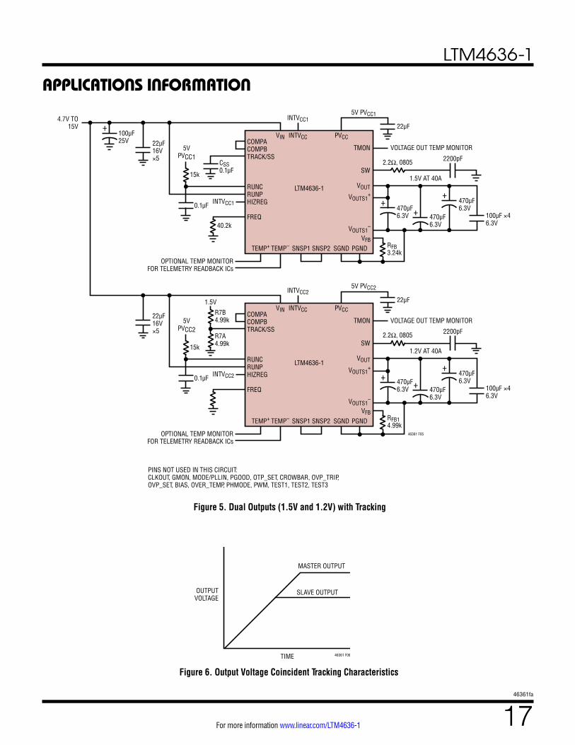
Figure 5. Dual Outputs (1.5V and 1.2V) with Tracking
Figure 6. Output Voltage Coincident Tracking Characteristics
46361 F06TIME
SLAVE OUTPUT
MASTER OUTPUT
OUTPUTVOLTAGE
+
COMPACOMPBTRACK/SS
RUNCRUNPHIZREG
FREQ
TMON
SW
VOUT
TEMP+ TEMP– SNSP1 SNSP2 SGND
VIN
15k
5VPVCC1
1.5V AT 40A
2.2Ω, 0805 2200pF
40.2k
CSS0.1µF
22µF
VOLTAGE OUT TEMP MONITOR
0.1µF
22µF16V×5
4.7V TO15V
100µF25V
INTVCC1
OPTIONAL TEMP MONITORFOR TELEMETRY READBACK ICs
INTVCC
INTVCC15V PVCC1
LTM4636-1
PVCC
PGND
VOUTS1+
VOUTS1–
VFB
+
470µF6.3V 470µF
6.3V
++
470µF6.3V
RFB3.24k
100µF ×46.3V
46361 F05
+
COMPACOMPBTRACK/SS
RUNCRUNPHIZREG
FREQ
TMON
SW
VOUT
TEMP+ TEMP– SNSP1 SNSP2 SGND
VIN
15k
1.5V
5VPVCC2
1.2V AT 40A
R7B4.99k
R7A4.99k
22µF
VOLTAGE OUT TEMP MONITOR
0.1µF
22µF16V×5
INTVCC2
OPTIONAL TEMP MONITORFOR TELEMETRY READBACK ICs
INTVCC
INTVCC25V PVCC2
LTM4636-1
PVCC
PGND
VOUTS1+
VOUTS1–
VFB
470µF6.3V 470µF
6.3V
++
470µF6.3V
RFB14.99k
100µF ×46.3V
2.2Ω, 0805 2200pF
PINS NOT USED IN THIS CIRCUIT:CLKOUT, GMON, MODE/PLLIN, PGOOD, OTP_SET, CROWBAR, OVP_TRIP, OVP_SET, BIAS, OVER_TEMP, PHMODE, PWM, TEST1, TEST2, TEST3
LTM4636-1
1846361fa
For more information www.linear.com/LTM4636-1
APPLICATIONS INFORMATIONRatiometric tracking can be achieved by a few simple calculations and the slew rate value applied to the master’s TRACK/SS pin. As mentioned above, the TRACK/SS pin has a control range from 0V to 0.6V. The master’s TRACK/SS pin slew rate is directly equal to the master’s output slew rate in volts/time. The equation:
MRSR
• 4.99k R TB
where MR is the master’s output slew rate and SR is the slave’s output slew rate in volts/time. When coincident tracking is desired, then MR and SR are equal, thus RTB is equal to 60.4k. RTA is derived from equation:
R TA0.6V
VFB4.99k
VFBRFB1
–V TRACK
R TB
where VFB is the feedback voltage reference of the regula-tor, and VTRACK is 0.6V. Since RTB is equal to the 4.99k top feedback resistor of the slave regulator in equal slew rate or coincident tracking, then RTA is equal to RFB with VFB = VTRACK. Therefore RTB = 4.99k, and RTA = 4.99k in Figure 5.
In ratiometric tracking, a different slew rate maybe desired for the slave regulator. RTB can be solved for when SR is slower than MR. Make sure that the slave supply slew rate is chosen to be fast enough so that the slave output voltage will reach its final value before the master output.
For example, MR = 1.5V/ms, and SR = 1.2V/ms. Then RTB = 6.19k. Solve for RTA to equal 4.22k.
For applications that do not require tracking or sequenc-ing, simply tie the TRACK/SS pin to INTVCC to let RUN control the turn on/off. When the RUN pin is below its threshold or the VIN undervoltage lockout, then TRACK/SS is pulled low.
Default Overcurrent and Overvoltage Protection
The LTM4636-1 has overcurrent protection (OCP) in a short circuit. The internal current comparator threshold folds back during a short to reduce the output current. An overvoltage condition (OVP) above 10% of the regulated
output voltage will force the top MOSFET off and the bottom MOSFET on until the condition is cleared. Foldback current limiting is disabled during soft-start or tracking start-up.
Temperature Monitoring
Measuring the absolute temperature of a diode is pos-sible due to the relationship between current, voltage and temperature described by the classic diode equation:
ID IS • eVD• VT
or
VD • VT •InIDIS
where ID is the diode current, VD is the diode voltage, is the ideality factor (typically close to 1.0) and IS (satu-ration current) is a process dependent parameter. VT can be broken out to:
VT
k • Tq
where T is the diode junction temperature in Kelvin, q is the electron charge and k is Boltzmann’s constant. VT is approximately 26mV at room temperature (298K) and scales linearly with Kelvin temperature. It is this linear temperature relationship that makes diodes suitable tem-perature sensors. The IS term in the previous equation is the extrapolated current through a diode junction when the diode has zero volts across the terminals. The IS term varies from process to process, varies with temperature, and by definition must always be less than ID. Combining all of the constants into one term:
KD
•kq
where KD = 8.62−5, and knowing ln(ID/IS) is always posi-tive because ID is always greater than IS, leaves us with the equation that:
VD T KELVIN •KD •In
IDIS
LTM4636-1
1946361fa
For more information www.linear.com/LTM4636-1
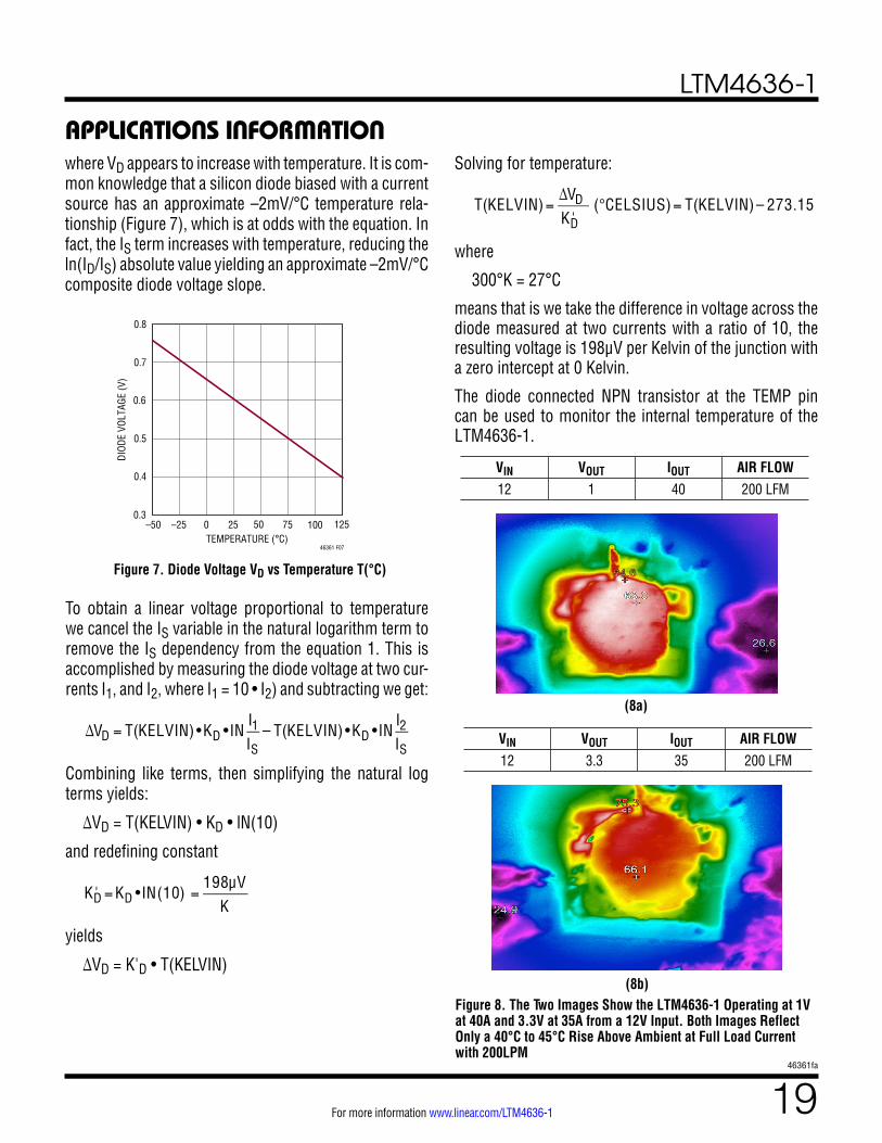
where VD appears to increase with temperature. It is com-mon knowledge that a silicon diode biased with a current source has an approximate –2mV/°C temperature rela-tionship (Figure 7), which is at odds with the equation. In fact, the IS term increases with temperature, reducing the ln(ID/IS) absolute value yielding an approximate –2mV/°C composite diode voltage slope.
APPLICATIONS INFORMATION
To obtain a linear voltage proportional to temperature we cancel the IS variable in the natural logarithm term to remove the IS dependency from the equation 1. This is accomplished by measuring the diode voltage at two cur-rents I1, and I2, where I1 = 10 • I2) and subtracting we get:
∆VD T(KELVIN) •KD •IN
I1IS
– T(KELVIN) •KD •INI2IS
Combining like terms, then simplifying the natural log terms yields:
∆VD = T(KELVIN) • KD • lN(10)
and redefining constant
K'D KD •IN(10)
198µVK
yields
∆VD = K'D • T(KELVIN)
Figure 7. Diode Voltage VD vs Temperature T(°C)
TEMPERATURE (°C)–50 –25
0.3
DIOD
E VO
LTAG
E (V
)
0.5
0.8
0 50 75
0.4
0.7
0.6
25 100
46361 F07
125
Solving for temperature:
T(KELVIN)∆VDK'D
( CELSIUS) T(KELVIN)– 273.15
where
300°K = 27°C
means that is we take the difference in voltage across the diode measured at two currents with a ratio of 10, the resulting voltage is 198μV per Kelvin of the junction with a zero intercept at 0 Kelvin.
The diode connected NPN transistor at the TEMP pin can be used to monitor the internal temperature of the LTM4636-1.
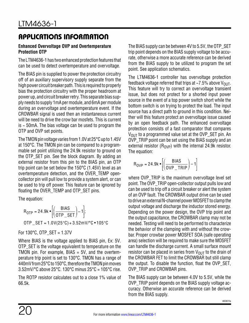
Figure 8. The Two Images Show the LTM4636-1 Operating at 1V at 40A and 3.3V at 35A from a 12V Input. Both Images Reflect Only a 40°C to 45°C Rise Above Ambient at Full Load Current with 200LPM
(8b)
(8a)
VIN VOUT IOUT AIR FLOW12 1 40 200 LFM
VIN VOUT IOUT AIR FLOW12 3.3 35 200 LFM
LTM4636-1
2046361fa
For more information www.linear.com/LTM4636-1
APPLICATIONS INFORMATIONEnhanced Overvoltage OVP and Overtemperature Protection OTP
The LTM4636-1 has two enhanced protection features that can be used to detect overtemperature and overvoltage.
The BIAS pin is supplied to power the protection circuitry off of an auxiliary supervisory supply separate from the high power circuit breaker path. This is required to properly bias the protection circuitry with the proper headroom at power up, and circuit breaker retry. This separate bias sup-ply needs to supply 1mA per module, and 6mA per module during an overvoltage and overtemperature event. If the CROWBAR signal is used then an instantaneous current will be need to drive the crow bar mosfets. This is current is ~ 50mA. The bias voltage can be used to program the OTP and OVP set points.
The TMON pin voltage varies from 1.0V at 25°C up to 1.45V at 150°C. The TMON pin can be compared to a program-mable set point utilizing the 24.9k resistor to ground on the OTP_SET pin. See the block diagram. By adding an external resistor from this pin to the BIAS pin, an OTP trip point can be set below the 150°C (1.45V) level as an overtemperature detection, and the OVER_TEMP open-collector pin will pull low to provide a system alert, or can be used to trip off power. This feature can be ignored by floating the OVER_TEMP and OTP_SET pins.
The equation:
ROTP 24.9k •BIAS
OTP _ SET1 ;
OTP _ SET 1.0V(25 C) 3.52mV/°C • 105 C
For 130°C, OTP_SET = 1.37V
Where BIAS is the voltage applied to BIAS pin, Ex: 5V. OTP_SET is the voltage equivalent to temperature on the TMON pin. For example, BIAS = 5V, and the overtem-perature trip point is set to 130°C. TMON has a range of 440mV from 25°C to 150°C, therefore the TMON pin moves 3.52mV/°C above 25°C. 130°C minus 25°C = 105°C rise.
The ROTP resistor calculates out to a close 1% value of 66.5k.
The BIAS supply can be between 4V to 5.5V, the OTP_SET trip point depends on the BIAS supply voltage to be accu-rate, otherwise a more accurate reference can be derived from the BIAS supply to be utilized to program the set point. See application schematics.
The LTM4636-1 controller has overvoltage protection feedback voltage referred that trips at ~7.5% above VOUT. This feature will try to correct an overvoltage transient issue, but does not protect for a shorted input power source in the event of a top power switch short while the bottom switch is on trying to protect the load. The input source has a direct path to ground in this condition. Nei-ther will this feature protect an overvoltage issue caused by an open feedback path. The enhanced overvoltage protection consists of a fast comparator that compares VOUT to a programmed value set at the OVP_SET pin. An OVP_TRIP point can be set using the BIAS supply and an external resistor (ROVP) with the internal 24.9k resistor. The equation:
ROVP 24.9k •
BIASOVP _ TRIP
– 1
where OVP_TRIP is the maximum overvoltage level set point. The OVP_TRIP open-collector output pulls low and can be used to trip off a circuit breaker or alert the system of an OVP fault. The CROWBAR output drive can be used to drive an external N-channel power MOSFET to clamp the output voltage and discharge the inductor stored energy. Depending on the power design, the OVP trip point and the output capacitance, the CROWBAR clamp may not be needed. Testing will need to be performed to characterize the behavior of the clamping with and without the crow-bar. Proper crowbar power MOSFET SOA (safe operating area) selection will be required to make sure the MOSFET can handle the discharge current. A small surface mount resistor can be placed in series from VOUT to the drain of the CROWBAR FET to limit the CROWBAR but still clamp the output. To disable the function, float the OVP_SET, OVP_TRIP and CROWBAR pins.
The BIAS supply can be between 4.0V to 5.5V, while the OVP_TRIP point depends on the BIAS supply voltage ac-curacy. Otherwise an accurate reference can be derived from the BIAS supply.
LTM4636-1
2146361fa
For more information www.linear.com/LTM4636-1
APPLICATIONS INFORMATIONRUNP and RUNC Enable
The RUNP pin is used to enable the 5V PVCC supply that powers the power driver stage and enables the power stage ~1ms later. The RUNC pin is used to enable the control section that drives the power stage. The RUNP needs to be enabled first, and then RUNC. RUNP has a 0.85V threshold and can be connected to the input voltage and RUNC has a 1.35V threshold and a 10k resistor to ground. See the Block Diagram for details. A 0.1µF capacitor from the RUNC pin to ground is used to set the delay for RUNC enable.
INTVCC and PVCC Regulators
The LTM4636-1 has an internal low dropout regulator from VIN called INTVCC. This regulator output has a 4.7μF ceramic capacitor internal. This regulator powers the control section. The PVCC 5V regulator supplies power to the power MOSFET driver stage. An additional 50mA can be used from this 5V PVCC supply for other needs. The input supply source resistance needs to be very low in order to minimize IR drops when operating from a 5V input source. Depending on the output voltage and current, the input supply can source large current,and PVCC 5V regulator needs a minimum 4.7V supply. Additional input capacitance maybe needed for 5V inputs to limit the input droop.
Stability Compensation
The LTM4636-1 has already been internally compensated when COMPB is tied to COMPA for all output voltages. Table 5 is provided for most application requirements. For specific optimized requirements, disconnect COMPB from COMPA, and use LTpowerCAD to perform specific control loop optimization. Then select the desired external compensation and output capacitance for the desired optimized response.
SW Pins
The SW pins are generally for testing purposes by moni-toring these pins. These pins can also be used to dampen out switch node ringing caused by LC parasitic in the switched current paths. Usually a series R-C combina-tion is used called a snubber circuit. The resistor will dampen the resonance and the capacitor is chosen to only affect the high frequency ringing across the resistor.
If the stray inductance or capacitance can be measured or approximated then a somewhat analytical technique can be used to select the snubber values. The inductance is usually easier to predict. It combines the power path board inductance in combination with the MOSFET interconnect bond wire inductance.
First the SW pin can be monitored with a wide bandwidth scope with a high frequency scope probe. The ring fre-quency can be measured for its value. The impedance Z can be calculated:
Z(L) = 2πfL,
where f is the resonant frequency of the ring, and L is the total parasitic inductance in the switch path. If a resistor is selected that is equal to Z, then the ringing should be dampened. The snubber capacitor value is chosen so that its impedance is equal to the resistor at the ring frequency. Calculated by: Z(C) = 1/(2πfC). These values are a good place to start with. Modification to these components should be made to attenuate the ringing with the least amount of power loss. A recommended value of 2.2Ω in series with 2200pF to ground should work for most ap-plications. See Figure 19 for layout guidelines. The 2.2Ω resistor should be an 0805 size.
Thermal Considerations and Output Current Derating
The thermal resistances reported in the Pin Configuration section of the data sheet are consistent with those param-eters defined by JESD51-12 and are intended for use with finite element analysis (FEA) software modeling tools that leverage the outcome of thermal modeling, simulation, and correlation to hardware evaluation performed on a µModule package mounted to a hardware test board. The motivation for providing these thermal coefficients in found in JESD51-12 (“Guidelines for Reporting andUsing Electronic Package Thermal Information”).
Many designers may opt to use laboratory equipment and a test vehicle such as the demo board to predict the µModule regulator’s thermal performance in their application at various electrical and environmental operating conditions to compliment any FEA activities. Without FEA software, the thermal resistances reported in the Pin Configuration section are, in and of themselves, not relevant to providing guidance of thermal performance; instead, the derating
LTM4636-1
2246361fa
For more information www.linear.com/LTM4636-1
APPLICATIONS INFORMATIONcurves provided in this data sheet can be used in a man-ner that yields insight and guidance pertaining to one’s application usage, and can be adapted to correlate thermal performance to one’s own application.
The Pin Configuration section gives four thermal coeffi-cients explicitly defined in JESD51-12; these coefficients are quoted or paraphrased below:
1. JA, the thermal resistance from junction to ambient, is the natural convection junction-to-ambient air ther-mal resistance measured in a one cubic foot sealed enclosure. This environment is sometimes referred to as “still air” although natural convection causes the air to move. This value is determined with the part mounted to a 95mm × 76mm PCB with four layers.
2. JCbottom, the thermal resistance from junction to the bottom of the product case, is determined with all of the component power dissipation flowing through the bottom of the package. In the typical µModule regulator, the bulk of the heat flows out the bottom of the package, but there is always heat flow out into the ambient environment. As a result, this thermal resistance value may be useful for comparing pack-ages but the test conditions don’t generally match the user’s application.
3 JCtop, the thermal resistance from junction to top of the product case, is determined with nearly all of the component power dissipation flowing through the top of the package. As the electrical connections of the typical µModule regulator are on the bottom of the
package, it is rare for an application to operate such that most of the heat flows from the junction to the top of the part. As in the case of JCbottom, this value may be useful for comparing packages but the test conditions don’t generally match the user’s application.
4 JB, the thermal resistance from junction to the printed circuit board, is the junction-to-board thermal resis-tance where almost all of the heat flows through the bottom of the µModule package and into the board, and is really the sum of the JCbottom and the thermal resistance of the bottom of the part through the solder joints and a portion of the board. The board temperature is measured a specified distance from the package.
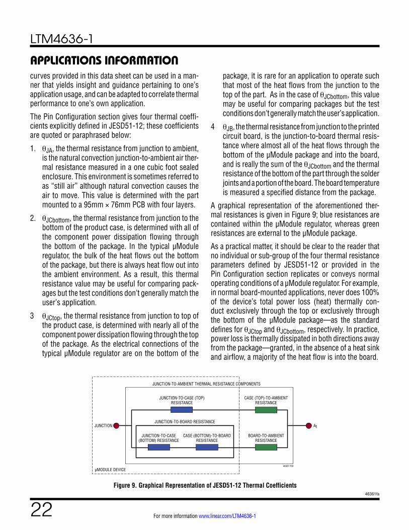
A graphical representation of the aforementioned ther-mal resistances is given in Figure 9; blue resistances are contained within the µModule regulator, whereas green resistances are external to the µModule package.
As a practical matter, it should be clear to the reader that no individual or sub-group of the four thermal resistance parameters defined by JESD51-12 or provided in the Pin Configuration section replicates or conveys normal operating conditions of a µModule regulator. For example, in normal board-mounted applications, never does 100% of the device’s total power loss (heat) thermally con-duct exclusively through the top or exclusively through the bottom of the µModule package—as the standard defines for JCtop and JCbottom, respectively. In practice, power loss is thermally dissipated in both directions away from the package—granted, in the absence of a heat sink and airflow, a majority of the heat flow is into the board.
Figure 9. Graphical Representation of JESD51-12 Thermal Coefficients
46361 F09
µMODULE DEVICE
JUNCTION-TO-CASE (TOP)RESISTANCE
JUNCTION-TO-BOARD RESISTANCE
JUNCTION-TO-AMBIENT THERMAL RESISTANCE COMPONENTS
CASE (TOP)-TO-AMBIENTRESISTANCE
BOARD-TO-AMBIENTRESISTANCE
JUNCTION-TO-CASE(BOTTOM) RESISTANCE
JUNCTION At
CASE (BOTTOM)-TO-BOARDRESISTANCE
LTM4636-1
2346361fa
For more information www.linear.com/LTM4636-1
APPLICATIONS INFORMATIONWithin the LTM4636-1, be aware there are multiple power devices and components dissipating power, with a con-sequence that the thermal resistances relative to different junctions of components or die are not exactly linear with respect to total package power loss. To reconcile this complication without sacrificing modeling simplicity—but also not ignoring practical realities—an approach has been taken using FEA software modeling along with laboratory testing in a controlled-environment chamber to reason-ably define and correlate the thermal resistance values supplied in this data sheet: (1) Initially, FEA software is used to accurately build the mechanical geometry of the LTM4636-1 and the specified PCB with all of the correct material coefficients along with accurate power loss source definitions; (2) this model simulates a software-defined JEDEC environment consistent with JESD51-12 to predict power loss heat flow and temperature readings at different interfaces that enable the calculation of the JEDEC-defined thermal resistance values; (3) the model and FEA software is used to evaluate the LTM4636-1 with heat sink and airflow; (4) having solved for and analyzed these thermal resistance values and simulated various operating conditions in the software model, a thorough laboratory evaluation replicates the simulated conditions with thermocouples within a controlled-environment chamber while operating the device at the same power loss as that which was simulated. The outcome of this process and due diligence yields the set of derating curves shown in this data sheet.
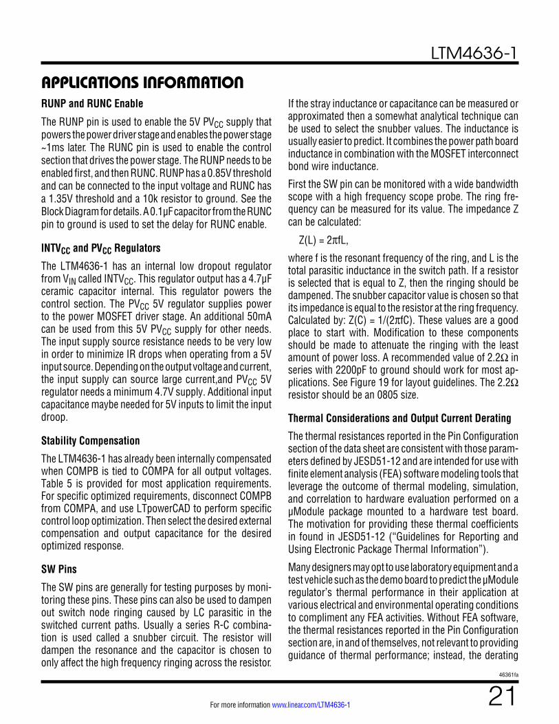
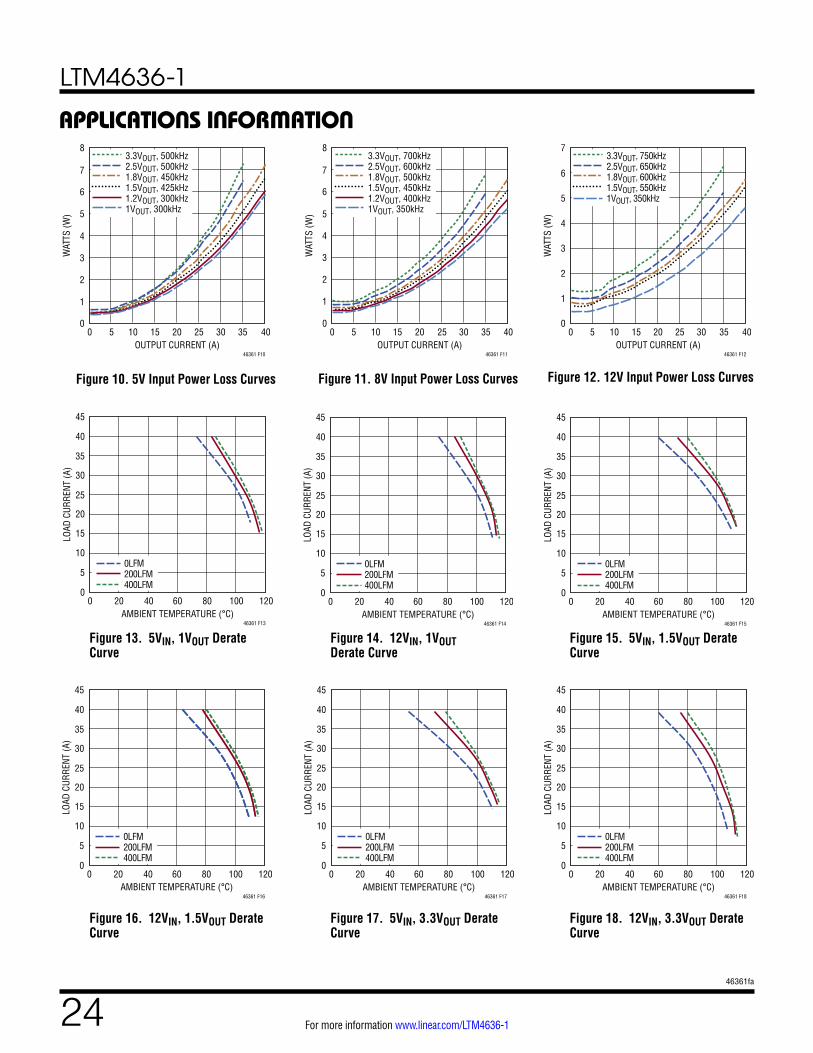
The power loss curves in Figure 10 to Figure 12 can be used in coordination with the load current derating curves in Figure 13 to Figure 18 for calculating an approximate JA thermal resistance for the LTM4636-1 with various airflow conditions. The power loss curves are taken at room temperature and can be increased with a multiplicative factor according to the junction temperature, which is ~1.4 for 120°C. The derating curves are plotted with the output current starting at 40A and the ambient temperature increased. The output voltages are 1V, 2.5V and 3.3V. These are chosen to include the lower, middle and higher output voltage ranges for correlating the thermal resistance. Thermal models are derived from several temperature measurements in a controlled temperature chamber along with thermal modeling analysis. The junction temperatures are monitored while
ambient temperature is increased with and without airflow. The power loss increase with ambient temperature change is factored into the derating curves. The junctions are maintained at ~125°C maximum while lowering output current or power with increasing ambient temperature. The decreased output current will decrease the internal module loss as ambient temperature is increased. The monitored junction temperature of 125°C minus the ambient operating temperature specifies how much module temperature rise can be allowed. As an example, in Figure 14 the load current is derated to ~30A at ~94°C with no air flow and the power loss for the 12V to 1.0V at 30A output is about 4.2W. The 4.2W loss is calculated with the ~3W room temperature loss from the 12V to 1.0V power loss curve at 30A, and the 1.4 multiplying factor at 125°C junction. If the 94°C ambient temperature is subtracted from the 125°C junction temperature, then the difference of 31°C divided by 4.2W equals a 7.4°C/W
JA thermal resistance. Table 2 specifies a 7.2°C/W value which is very close. Tables 2, 3, and 4 provide equivalent thermal resistances for 1V, 1.5V and 3.3V outputs with and without airflow and heat sinking. The derived thermal resistances in Tables 2 thru 4 for the various conditions can be multiplied by the calculated power loss as a function of ambient temperature to derive temperature rise above ambient, thus maximum junction temperature. Room temperature power loss curves are provided in Figure 10 through Figure 12. The printed circuit board is a 1.6mm thick six layer board with two ounce copper for all layers and one ounce copper for the two inner layers. The PCB dimensions are 95mm × 76mm.
Safety Considerations
The LTM4636-1 does not provide galvanic isolation from VIN to VOUT. There is no internal fuse. If required, a slow blow fuse with a rating twice the maximum input current needs to be provided to protect each unit from catastrophic failure.
The fuse or circuit breaker should be selected to limit the current to the regulator during overvoltage in case of an internal top MOSFET fault. If the internal top MOSFET fails, then turning it off will not resolve the overvoltage, thus the internal bottom MOSFET will turn on indefinitely trying to protect the load. Under this fault condition, the
LTM4636-1
2446361fa
For more information www.linear.com/LTM4636-1
APPLICATIONS INFORMATION
Figure 10. 5V Input Power Loss Curves Figure 11. 8V Input Power Loss Curves
OUTPUT CURRENT (A)0
WAT
TS (W
)
8
5
3
6
7
4
2
1
02515 4035
46361 F10
20105 30
3.3VOUT, 500kHz2.5VOUT, 500kHz1.8VOUT, 450kHz1.5VOUT, 425kHz1.2VOUT, 300kHz1VOUT, 300kHz
OUTPUT CURRENT (A)0
WAT
TS (W
)
8
5
3
6
7
4
2
1
02515 4035
46361 F11
20105 30
3.3VOUT, 700kHz2.5VOUT, 600kHz1.8VOUT, 500kHz1.5VOUT, 450kHz1.2VOUT, 400kHz1VOUT, 350kHz
OUTPUT CURRENT (A)0
WAT
TS (W
)
7
5
3
6
4
2
1
02515 40
46361 F12
20105 30 35
3.3VOUT, 750kHz2.5VOUT, 650kHz1.8VOUT, 600kHz1.5VOUT, 550kHz1VOUT, 350kHz
AMBIENT TEMPERATURE (°C)0
LOAD
CUR
RENT
(A)
45
35
25
40
30
20
15
10
5
060 120
46361 F13
4020 80 100
0LFM200LFM400LFM
0
45
35
25
40
30
20
15
10
5
060 120
46361 F14
4020 80 100
0LFM200LFM400LFM
AMBIENT TEMPERATURE (°C)
LOAD
CUR
RENT
(A)
0
45
35
25
40
30
20
15
10
5
060 120
46361 F15
4020 80 100
0LFM200LFM400LFM
AMBIENT TEMPERATURE (°C)
LOAD
CUR
RENT
(A)
0
45
35
25
40
30
20
15
10
5
060 120
46361 F16
4020 80 100
0LFM200LFM400LFM
AMBIENT TEMPERATURE (°C)
LOAD
CUR
RENT
(A)
0
45
35
25
40
30
20
15
10
5
060 120
46361 F17
4020 80 100
0LFM200LFM400LFM
AMBIENT TEMPERATURE (°C)
LOAD
CUR
RENT
(A)
0
45
35
25
40
30
20
15
10
5
060 120
46361 F18
4020 80 100
0LFM200LFM400LFM
AMBIENT TEMPERATURE (°C)
LOAD
CUR
RENT
(A)
Figure 12. 12V Input Power Loss Curves
Figure 13. 5VIN, 1VOUT Derate Curve
Figure 14. 12VIN, 1VOUT Derate Curve
Figure 15. 5VIN, 1.5VOUT Derate Curve
Figure 16. 12VIN, 1.5VOUT Derate Curve
Figure 17. 5VIN, 3.3VOUT Derate Curve
Figure 18. 12VIN, 3.3VOUT Derate Curve
LTM4636-1
2546361fa
For more information www.linear.com/LTM4636-1
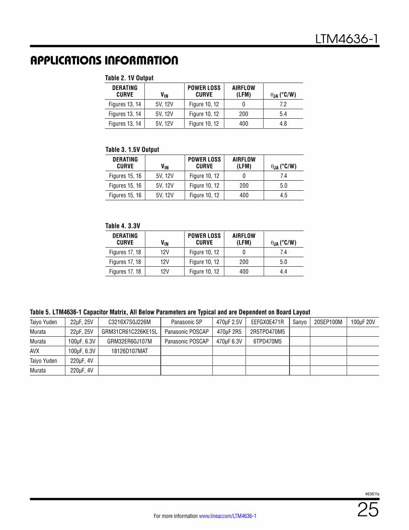
Table 2. 1V OutputDERATING
CURVE VIN POWER LOSS
CURVEAIRFLOW
(LFM) JA (°C/W)
Figures 13, 14 5V, 12V Figure 10, 12 0 7.2
Figures 13, 14 5V, 12V Figure 10, 12 200 5.4
Figures 13, 14 5V, 12V Figure 10, 12 400 4.8
Table 3. 1.5V OutputDERATING
CURVE VIN POWER LOSS
CURVEAIRFLOW
(LFM) JA (°C/W)
Figures 15, 16 5V, 12V Figure 10, 12 0 7.4
Figures 15, 16 5V, 12V Figure 10, 12 200 5.0
Figures 15, 16 5V, 12V Figure 10, 12 400 4.5
Table 4. 3.3VDERATING
CURVE VIN POWER LOSS
CURVEAIRFLOW
(LFM) JA (°C/W)
Figures 17, 18 12V Figure 10, 12 0 7.4
Figures 17, 18 12V Figure 10, 12 200 5.0
Figures 17, 18 12V Figure 10, 12 400 4.4
APPLICATIONS INFORMATION
Table 5. LTM4636-1 Capacitor Matrix, All Below Parameters are Typical and are Dependent on Board LayoutTaiyo Yuden 22µF, 25V C3216X7S0J226M Panasonic SP 470µF 2.5V EEFGX0E471R Sanyo 20SEP100M 100µF 20V
Murata 22µF, 25V GRM31CR61C226KE15L Panasonic POSCAP 470µF 2R5 2R5TPD470M5
Murata 100µF, 6.3V GRM32ER60J107M Panasonic POSCAP 470µF 6.3V 6TPD470M5
AVX 100µF, 6.3V 18126D107MAT
Taiyo Yuden 220µF, 4V
Murata 220µF, 4V
LTM4636-1
2646361fa
For more information www.linear.com/LTM4636-1
APPLICATIONS INFORMATION
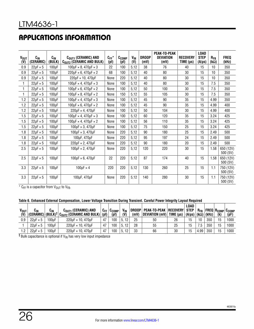
Table 6. Enhanced External Compensation, Lower Voltage Transition During Transient. Careful Power Integrity Layout Required
VOUT (V)
CIN (CERAMIC)
CIN (BULK)†
COUT1 (CERAMIC) AND COUT2 (CERAMIC AND BULK)
CFF (pf)
CCOMP (pf)
VIN (V)
DROOP (mV)
PEAK-TO-PEAK DEVIATION (mV)
RECOVERY TIME (µs)
LOAD STEP (A/µs)
RFB (kΩ)
FREQ (kHz)
RCOMP (k)
CCOMP (pF)
0.9 22µF × 5 100µF 220µF × 10, 470µF 47 100 5, 12 25 50 26 15 10 350 15 10001 22µF × 5 100µF 220µF × 10, 470µF 47 100 5, 12 28 55 25 15 7.5 350 15 1000
1.2 22µF × 5 100µF 220µF × 10, 470µF 47 100 5, 12 33 66 30 15 4.99 350 15 1000† Bulk capacitance is optional if VIN has very low input impedance
VOUT (V)
CIN (CERAMIC)
CIN (BULK)
COUT1 (CERAMIC) AND COUT2 (CERAMIC AND BULK)
CFF* (pf)
CCOMP (pf)
VIN (V)
DROOP (mV)
PEAK-TO-PEAK DEVIATION
(mV)RECOVERY TIME (µs)
LOAD STEP (A/µs)
RFB (kΩ)
FREQ (kHz)
0.9 22µF × 5 100µF 100µF × 8, 470µF × 3 22 100 5,12 38 76 40 15 10 3500.9 22µF × 5 100µF 220µF × 6, 470µF × 2 68 100 5,12 40 80 30 15 10 3500.9 22µF × 5 100µF 220µF × 10, 470µF None 220 5,12 40 80 30 15 10 3501 22µF × 5 100µF 100µF × 4, 470µF × 3 None 100 5,12 40 80 30 15 7.5 3501 22µF × 5 100µF 100µF × 6, 470µF × 2 None 100 5,12 50 100 30 15 7.5 3501 22µF × 5 100µF 100µF × 8, 470µF × 2 None 150 5,12 55 105 30 15 7.5 350
1.2 22µF × 5 100µF 100µF × 4, 470µF × 3 None 100 5,12 45 90 35 15 4.99 3501.2 22µF × 5 100µF 100µF × 6, 470µF × 2 None 100 5,12 45 90 35 15 4.99 4001.2 22µF × 5 100µF 220µF × 4, 470µF None 100 5,12 50 104 30 15 4.99 4001.5 22µF × 5 100µF 100µF × 4, 470µF × 3 None 100 5,12 60 120 35 15 3.24 4251.5 22µF × 5 100µF 100µF × 4, 470µF × 2 None 100 5,12 56 110 35 15 3.24 4251.5 22µF × 5 100µF 100µF × 3, 470µF None 100 5,12 75 150 25 15 3.24 4251.8 22µF × 5 100µF 100µF × 3, 470µF None 220 5,12 90 180 25 15 2.49 5001.8 22µF × 5 100µF 100µF, 470µF None 220 5,12 95 197 24 15 2.49 5001.8 22µF × 5 100µF 220µF × 2, 470µF None 220 5,12 90 180 20 15 2.49 5002.5 22µF × 5 100µF 100µF × 2, 470µF None 220 5,12 120 220 30 15 1.58 650 (12V)
500 (5V)2.5 22µF × 5 100µF 100µF × 6, 470µF 22 220 5,12 87 174 40 15 1.58 650 (12V)
500 (5V)3.3 22µF × 5 100µF 100µF × 4 220 220 5,12 130 260 25 15 1.1 750 (12V)
500 (5V)3.3 22µF × 5 100µF 100µF, 470µF None 220 5,12 140 280 30 15 1.1 750 (12V)
500 (5V)* CFF is a capacitor from VOUT to VFB.
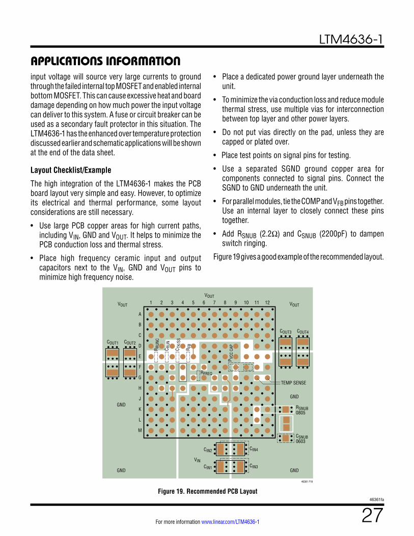
LTM4636-1
2746361fa
For more information www.linear.com/LTM4636-1
APPLICATIONS INFORMATIONinput voltage will source very large currents to ground through the failed internal top MOSFET and enabled internal bottom MOSFET. This can cause excessive heat and board damage depending on how much power the input voltage can deliver to this system. A fuse or circuit breaker can be used as a secondary fault protector in this situation. The LTM4636-1 has the enhanced over temperature protection discussed earlier and schematic applications will be shown at the end of the data sheet.
Layout Checklist/Example
The high integration of the LTM4636-1 makes the PCB board layout very simple and easy. However, to optimize its electrical and thermal performance, some layout considerations are still necessary.
• Use large PCB copper areas for high current paths, including VIN, GND and VOUT. It helps to minimize the PCB conduction loss and thermal stress.
• Place high frequency ceramic input and output capacitors next to the VIN, GND and VOUT pins to minimize high frequency noise.
• Place a dedicated power ground layer underneath the unit.
• To minimize the via conduction loss and reduce module thermal stress, use multiple vias for interconnection between top layer and other power layers.
• Do not put vias directly on the pad, unless they are capped or plated over.
• Place test points on signal pins for testing.
• Use a separated SGND ground copper area for components connected to signal pins. Connect the SGND to GND underneath the unit.
• For parallel modules, tie the COMP and VFB pins together. Use an internal layer to closely connect these pins together.
• Add RSNUB (2.2Ω) and CSNUB (2200pF) to dampen switch ringing.
Figure 19 gives a good example of the recommended layout.
Figure 19. Recommended PCB Layout
1
M
L
K
J
H
G
F
E
D
C
B
A
2 3 4 5 6 7
VOUT
VOUT
COUT1
CIN2
CIN1
CIN4
CIN3
COUT2
R RUN
C
VOUT
GND
TEMP SENSE
GND
GND
46361 F19
VIN
GND
8 9 10 11 12
COUT3 COUT4
C RUN
C TK/
SS
R FB
P VCC
CAP
RFREQ
RSNUB0805
CSNUB0603
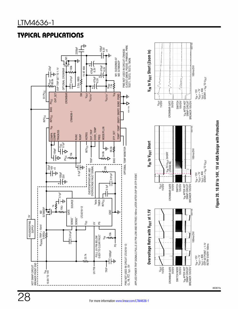
LTM4636-1
2846361fa
For more information www.linear.com/LTM4636-1
Figu
re 2
0. 1
0.8V
to 1
4V, 1
V at
40A
Des
ign
with
Pro
tect
ion
V IN
to V
OUT S
hort
(Zoo
m In
)V I
N to
VOU
T Sho
rtOv
ervo
ltage
Ret
ry w
ith V
OUT a
t 1.1
V
TYPICAL APPLICATIONS
+
COM
PACO
MPB
TRAC
K/SS
V OUTSW
TEM
P+TE
MP–
SNSP
1SN
SP2
SGND
V IN
100p
F
5V P
V CC
C SS
0.1µ
F
22µF
1V A
T 40
A
2.2Ω
, 080
50.
1µF
V IN
10.8
V TO
14V
100µ
F25
V
22µF
16V
×5
OPTI
ONAL
TEM
P M
ONIT
OR
INTV
CC
INTV
CC
LTM
4636
-1
PVCC
PGND
V OUT
S1+
V OUT
S1–
V FB
BIAS
+
470µ
F6.
3V
470µ
F6.
3V
+
+
470µ
F6.
3V
R FB2
7.5k
4636
1 F2
0a
PINS
NOT
USE
D IN
CIR
CUIT
LTM
4636
:CL
KOUT
, GM
ON, P
GOOD
, PHM
ODE,
PW
M,
TEST
1, T
EST2
, TES
T3, T
MON
2200
pF
OVP_
SET
CROW
BAR
OPTI
ONAL
CRO
WBA
R
OVP
TRIP
SET
TO
1.1V
R OVP
86.6
k
0.01
µF10
0k
M1
34.8
kINTV
CC
PVCC
MOD
E/PL
LIN
15k
RUNC
RUNP
HIZR
EG
BIAS
OTP_
SET
OVER
_TEM
POV
P_TR
IPTR
IP
FREQ
TIM
ER
I MON
LTC4
218-
12
GND
INTV
CC
GATE
M2
Si78
80DP
5V
PG
PG
20k
0.1µ
F
SENS
E–SO
URCE
V DD
SENS
E+
UV
OVER
TEM
PERA
TURE
AND
OV
ERVO
LTAG
E FA
ULT
SIGN
AL
100µ
F6.
3V×4
M1:
SUD
50N0
3-07
M2:
Si7
880A
DP
1000
pFTR
IP
PULL
UV
PIN
BELO
W0.
62V
TO C
LEAR
FAU
LT
UV P
IN
0.1µ
F
0.01
µF
10Ω
0.01
µF
23.7
k
1k
66.5
k
R SEN
SE T
RIP
= 15
mV
0.00
2Ω
HOUS
EKEE
PING
SUPP
LYHO
T SW
AP C
IRCU
ITBR
EAKE
R FR
ONT
END
V IN 10
k
PINS
NOT
USE
D IN
CIR
CUIT
LTC
4218
-12:
CL, F
B, FLT
, ISE
T, O
V
APPL
IED
POW
ER T
RIP
SIGN
ALS
PULL
S UV
PIN
LOW
AND
RET
RIES
100
ms
LATE
R AF
TER
OVP
OR O
TP E
VENT
.
V IN
= 12
VV O
UT =
1V
I OUT
= 4
0AOV
P SE
TPOI
NT =
1.1
VRE
TRY
EVER
Y 10
0ms
V OUT
1V/D
IV
CROW
BAR
GATE
5V/D
IV
SWIT
CH N
ODE
10V/
DIV
V IN
AFTE
R HO
TSW
AP C
IRCU
ITBR
EAKE
R 10
V/DI
V10
0ms/
DIV
4636
1 F2
0b
V IN
= 12
VV O
UT =
1V
I OUT
= 4
0ASH
ORT
= V I
N TO
VOU
T
V OUT
1V/D
IV
CROW
BAR
GATE
5V/D
IV
SWIT
CH10
V/DI
V
V IN
AFTE
R HO
TSW
AP C
IRCU
ITBR
EAKE
R 10
V/DI
V10
0ms/
DIV
V IN
TO V
OUT
SHOR
T(Z
OOM
IN)
4636
1 F2
0c
V IN
= 12
VV O
UT =
1V
I OUT
= 4
0ASH
ORT
= V I
N TO
VOU
T
V OUT
1V/D
IV
CROW
BAR
GATE
5V/D
IV
SWIT
CH10
V/DI
V
V IN
AFTE
R HO
TSW
AP C
IRCU
ITBR
EAKE
R 10
V/DI
V10
0ms/
DIV
4636
1 F2
0d
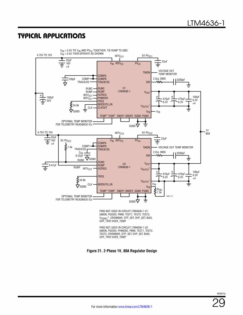
LTM4636-1
2946361fa
For more information www.linear.com/LTM4636-1
TYPICAL APPLICATIONS
Figure 21. 2-Phase 1V, 80A Regulator Design
7.5k
0.47µF
34.8k
4.75V TO 15V
4.75V TO 15V
++
COMPACOMPBTRACK/SS
RUNCRUNPHIZREG
FREQ
MODE/PLLIN
SW
TEMP+ TEMP– SNSP1 SNSP2 SGND
VIN
34.8k
CLK
INTVCC2
22µF
1V80A
22µF16V×4
CSS0.22µF
COMP
5V, PVCC2
TRACK/SS
RUNC
RUNP
OPTIONAL TEMP MONITORFOR TELEMETRY READBACK ICs
INTVCC
INTVCC2 5V PVCC2
U2LTM4636-1
PVCC
PGND
VOUTS1+
VOUT
VOUTS1–
VFBVFB
RFB27.5k
46361 F21
TMON VOLTAGE OUT TEMP MONITOR
470µF6.3V
470µF6.3V
100µF6.3V×4
+
COMPACOMPBTRACK/SS
RUNCRUNPHIZREGPHMODEFREQMODE/PLLINCLKOUT
TMON
SW
VOUT
TEMP+ TEMP– SNSP1 SNSP2 SGND
VIN22µF
2200pF
VOLTAGE OUTTEMP MONITOR
2.2Ω, 0805
22µF16V×4
VIN ≤ 5.5V, TIE VIN AND PVCC TOGETHER, TIE RUNP TO GND. VIN > 5.5V, THEN OPERATE AS SHOWN
INTVCC1
RUNCRUNP
CLK
COMPTRACK/SS
OPTIONAL TEMP MONITORFOR TELEMETRY READBACK ICs
INTVCC
INTVCC1 5V PVCC1
U1LTM4636-1
PVCC
PGND
VOUTS1–
VFBVFB
INTVCC1 470µF6.3V
+470µF6.3V
+100µF25V
100µF6.3V×4
2200pF2.2Ω, 0805
SGND
SGND
SGND
SGND
SGND
100pF
PINS NOT USED IN CIRCUIT LTM4636-1 U1:GMON, PGOOD, PWM, TEST1, TEST2, TEST3, VOSNS1
+, CROWBAR, OTP_SET, OVP_SET, BIAS, OVP_TRIP, OVER_TEMP
PINS NOT USED IN CIRCUIT LTM4636-1 U2:GMON, PGOOD, PHMODE, PWM, TEST1, TEST2, TEST3, CROWBAR, OTP_SET, OVP_SET, BIAS, OVP_TRIP, OVER_TEMP
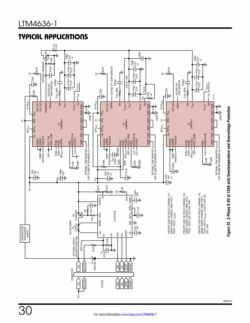
LTM4636-1
3046361fa
For more information www.linear.com/LTM4636-1
TYPICAL APPLICATIONS
Figu
re 2
2. 3
-Pha
se 0
.9V
at 1
20A
with
Ove
rtem
pera
ture
and
Ove
rvol
tage
Pro
tect
ion
+
COM
PACO
MPB
TRAC
K/SS
RUNC
RUNP
HIZR
EG
FREQ
MOD
E/PL
LIN
CLKO
UT
TMON SW
TEM
P+TE
MP–
SNSP
1SN
SP2
SGND
V IN
34.8
k
22µF
VOLT
AGE
OUT
TEM
P M
ONIT
OR
22µF
16V
×3
12V
INTV
CC1
RUNC
RUNP CL
K
COM
PTR
ACK/
SS
OPTI
ONAL
TEM
P M
ONIT
ORFO
R TE
LEM
ETRY
REA
DBAC
K IC
s
INTV
CC
INTV
CC1
5V P
V CC1
U1LT
M46
36-1
PVCC
PGND
V OUT
S1–
V FB
V FB
470µ
F6.
3V
+47
0µF
6.3V
+10
0µF
25V
100µ
F6.
3V×3
2.2Ω
, 080
522
00pF
4.99
k
0.47
µF
+
COM
PACO
MPB
TRAC
K/SS
RUNC
RUNP
HIZR
EGOV
ER_T
EMP
FREQ
MOD
E/PL
LIN
CLKO
UT
TMON SW
TEM
P+TE
MP–
SNSP
1SN
SP2
SGND
V IN
0.9V
AT
120A
CLK
CLK1
INTV
CC2
22µF
VOLT
AGE
OUT
TEM
P M
ONIT
OR
34.8
kC SS
0.22
µF
22µF
16V
×3
COM
PTR
ACK/
SS
RUNC
RUNP
OPTI
ONAL
TEM
P M
ONIT
ORFO
R TE
LEM
ETRY
REA
DBAC
K IC
s
INTV
CC
INTV
CC2
5V P
V CC2
U2LT
M46
36-1
PVCC
PGND
V OUT
S1–
V FB
V FB
4636
1 F2
2
TRIP
470µ
F6.
3V
+47
0µF
6.3V
R FB3
10k
100µ
F6.
3V×3
100µ
F
+
COM
PACO
MPB
TRAC
K/SS
RUNC
RUNP
HIZR
EGOV
ER_T
EMP
FREQ
MOD
E/PL
LIN
TMON SW
V OUT
V OUT
V OUT
S1+
V OUT
S1–
V OUT
S1–
V OUT
S1–
V OUT
S1–
V OUT
TEM
P+TE
MP–
SNSP
1SN
SP2
SGND
V IN
34.8
k
22µF
VOLT
AGE
OUT
TEM
P M
ONIT
OR
22µF
16V
×3
INTV
CC3
RUNC
RUNP
CLK1
COM
PTR
ACK/
SS
OPTI
ONAL
TEM
P M
ONIT
ORFO
R TE
LEM
ETRY
REA
DBAC
K IC
s
INTV
CC
INTV
CC3
5V P
V CC3
U3LT
M46
36-1
PVCC
PGNDV F
BV F
B
BIAS5V BIAS5V BIAS5V
OTP_
SET
OTP_
SET
OTP_
SET
TRIP
470µ
F6.
3V
+47
0µF
6.3V
100µ
F6.
3V×3
12V
PINS
NOT
USE
D IN
CIR
CUIT
LTM
4636
-1 U
1:GM
ON, P
GOOD
, PHM
ODE,
PW
M, T
EST1
, TE
ST2,
TES
T3, V
OUTS
1
PINS
NOT
USE
D IN
CIR
CUIT
LTM
4636
-1 U
2:GM
ON, P
GOOD
, PHM
ODE,
PW
M, T
EST1
, TE
ST2,
TES
T3, O
VP_S
ET, O
VP_T
RIP
PINS
NOT
USE
D IN
CIR
CUIT
LTM
4636
-1 U
3:GM
ON, P
GOOD
, PHM
ODE,
PW
M, T
EST1
, TE
ST2,
TES
T3, V
OUTS
1, C
LKOU
T, OV
P_SE
T, OV
P_TR
IP
2.2Ω
, 080
522
00pF
2.2Ω
, 080
522
00pF
SGND SG
ND
SGND
SGND
SGND
SGND
SGND
100p
F
OVP_
SET
66.5
k
0.1Ω
1210
102k
5V
66.5
k
5V
66.5
k
5V
V DD
SENS
E–
LTC4
215G
N
CONN
ECTO
ROP
TION
AL C
IRCU
ITBR
EAKE
R FR
ONT
END
GATE
INTV
CCSS
GND
ADR0
SOUR
CE
SDA
SCL
ALER
T
ONUV
GPIOFB
10Ω
10k
10nF
KELV
IN S
ENSE
R S0.
0015
ΩM
1Si
7880
ADP
28.7
k
3.57
k
12V 10
k
C F0.
01µF
34.6
k
TRIP
4.53
k
12V
SEAT
PIN
SYST
EM
SDA
SCL
ALER
T
BGGN
D
12V
SEAT
PIN
SDA
SCL
ALER
T
BGGN
D
12V
C SS
1nF
0.1µ
F
TIM
ER
C TIM
ER10
nF
D1P6
KE16
A
CROW
BAR
OPTI
ONAL
CRO
WBA
R
0.01
µF10
0k
M2
HOUS
EKEE
PING
SUPE
RVIS
ORY
SUPP
LY
OVER
_TEM
POV
P_TR
IPTR
IP
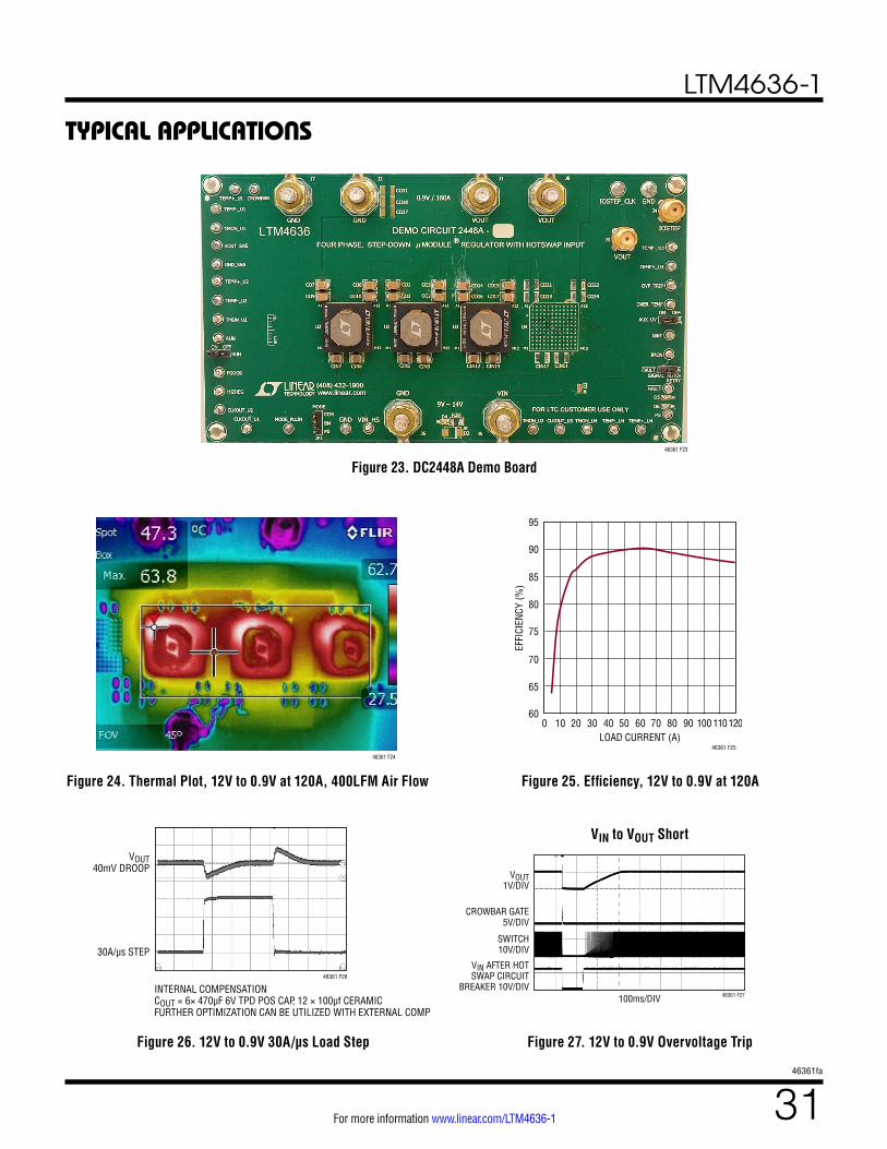
LTM4636-1
3146361fa
For more information www.linear.com/LTM4636-1
TYPICAL APPLICATIONS
LOAD CURRENT (A)0
EFFI
CIEN
CY (%
)95
85
75
90
80
70
65
6050 60 70 90 100 1104020 30 80
46361 F25
12010
46361 F26
VOUT40mV DROOP
30A/µs STEP
INTERNAL COMPENSATIONCOUT = 6× 470µF 6V TPD POS CAP, 12 × 100µf CERAMICFURTHER OPTIMIZATION CAN BE UTILIZED WITH EXTERNAL COMP
VIN to VOUT Short
VOUT1V/DIV
CROWBAR GATE5V/DIV
SWITCH10V/DIV
VIN AFTER HOTSWAP CIRCUIT
BREAKER 10V/DIV100ms/DIV 46361 F27
Figure 25. Efficiency, 12V to 0.9V at 120A
Figure 26. 12V to 0.9V 30A/µs Load Step Figure 27. 12V to 0.9V Overvoltage Trip
Figure 23. DC2448A Demo Board
46361 F24
Figure 24. Thermal Plot, 12V to 0.9V at 120A, 400LFM Air Flow
46361 F23
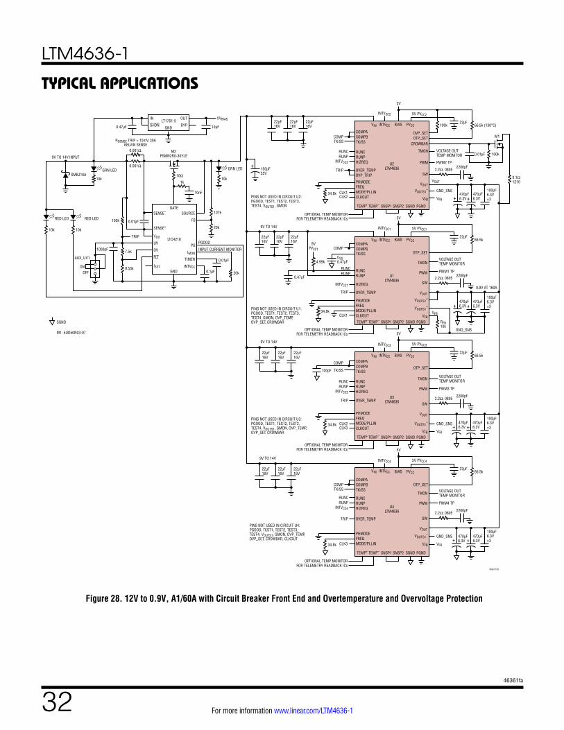
LTM4636-1
3246361fa
For more information www.linear.com/LTM4636-1
TYPICAL APPLICATIONS
Figure 28. 12V to 0.9V, A1/60A with Circuit Breaker Front End and Overtemperature and Overvoltage Protection
46361 F28
1k
0.001Ω
10nF
20k
10k
SOURCESENSE–
SENSE+
GND
GATE
LTC4218
FB
VDD
UV
OV IMON
TIMER
INTVCC
FLT
PG
ISET
PGOOD
10Ω
M2PSMN2R0-30YLE
RSENSE TRIP = 15mV, 30AKELVIN SENSE
107k
10k
100k
TRIP
10k
7.5k
ONOFF
AUX_UV1
9.53k
SMBJ16A
0.1µF
1000pF
0.01µF
0.01µF
20k
INPUT CURRENT MONITOR
GRN LED GRN LED
9V TO 14V INPUT
0.001Ω
10k
RED LEDRED LED
INLT1761-5
SHDN
OUT
BYPGND0.47µF 10µF
5VBIAS
+
COMPACOMPBTK/SS
RUNCRUNPHIZREG
OVP_SETOTP_SET
OTP_SET
TEMP+ TEMP– SNSP1 SNSP2 SGND
VIN
34.8k
22µF
100k
M1
0.01µF
100k
VOLTAGE OUTTEMP MONITOR
22µF16V
22µF16V
22µF16V
150µF35V
9V TO 14V
9V TO 14V
9V TO 14V
INTVCC2
RUNCRUNP
CLK2CLK1
COMPTK/SS
OPTIONAL TEMP MONITORFOR TELEMETRY READBACK ICs
INTVCC
INTVCC2 5V PVCC2
5V
U2LTM4636
PVCC
PGND
VFB
VOUTS1–
VFB
BIAS
PWM2 TP
470µF6.3V+
470µF6.3V
100µF6.3V×3
GND_SNS
2.2Ω, 08052200pF
2.2Ω, 08052200pF
VOUT
+
COMPACOMPB
TEMP+ TEMP– SNSP1 SNSP2 SGND
VIN
34.8k
4.99k
5VPVCC1
VOLTAGE OUTTEMP MONITOR
CSS0.47µF
0.47µF
TRIP
INTVCC1
RUNCRUNP
CLK1
COMP
OPTIONAL TEMP MONITORFOR TELEMETRY READBACK ICs
INTVCC
INTVCC1
U1LTM4636
PGNDVFB
VFB
PWM1 TP
470µF6.3V
RFB10k
+470µF6.3V
100µF6.3V×3VOUTS1
–
VOUTS1+
0.9V AT 160A
+
COMPACOMPBTK/SS
RUNCRUNPHIZREG
TMON
PWM
SW
VOUT
TEMP+ TEMP– SNSP1 SNSP2 SGND
VIN
34.8k
GND_SNS
VOLTAGE OUTTEMP MONITOR
INTVCC3
RUNCRUNP
CLK3CLK2
TK/SS
COMP
OPTIONAL TEMP MONITORFOR TELEMETRY READBACK ICs
PINS NOT USED IN CIRCUIT U2:PGOOD, TEST1, TEST2, TEST3, TEST4, VOUTS1, GMON
PINS NOT USED IN CIRCUIT U1:PGOOD, TEST1, TEST2, TEST3, TEST4, GMON, OVP_TEMP, OVP_SET, CROWBAR
PINS NOT USED IN CIRCUIT U3:PGOOD, TEST1, TEST2, TEST3, TEST4, VOUTS1, GMON, OVP_TEMP, OVP_SET, CROWBAR
PINS NOT USED IN CIRCUIT U4:PGOOD, TEST1, TEST2, TEST3, TEST4, VOUTS1, GMON, OVP_TEMP, OVP_SET, CROWBAR, CLKOUT
INTVCC
INTVCC3
U3LTM4636
PGNDVFB VFB
PWM3 TP
470µF6.3V+
470µF6.3V
100µF6.3V×3
GND_SNS
2.2Ω, 08052200pF
+
COMPACOMPBTK/SS
RUNCRUNPHIZREG
TMON
PWM
SW
VOUT
TEMP+ TEMP– SNSP1 SNSP2 SGND
VIN
34.8k
VOLTAGE OUTTEMP MONITOR
INTVCC4
RUNCRUNP
CLK3
COMPTK/SS
OPTIONAL TEMP MONITORFOR TELEMETRY READBACK ICs
INTVCC
INTVCC4
U4LTM4636
PGND
VFB
VOUTS1–
VFB
PWM4 TP
470µF6.3V
470µF6.3V
100µF6.3V×3
GND_SNS
2.2Ω, 08052200pF
100pF
VOUTS1–
+
22µF16V
22µF16V
22µF16V
22µF16V
22µF16V
22µF16V
22µF16V
22µF16V
22µF16V
PHMODEFREQMODE/PLLINCLKOUT
OVER_TEMP
66.5k (130°C)
22µF
5V PVCC1
5V
PVCCBIAS 66.5k
22µF
5V PVCC3
5V
PVCCBIAS 66.5k
OTP_SET
22µF
5V PVCC4
5V
PVCCBIAS 66.5k
OTP_SET
TMON
PWM
SW
VOUT
VOUT
TMON
CROWBAR
PWM
SW
+
RUNCRUNP
TK/SS
SGND
M1: 5UD50N03-07
OVER_TEMPOVP_TRIP
TRIP
OVER_TEMPTRIP
OVER_TEMPTRIP
PHMODEFREQMODE/PLLINCLKOUT
PHMODEFREQMODE/PLLINCLKOUT
PHMODEFREQMODE/PLLIN
0.1Ω1210
HIZREG
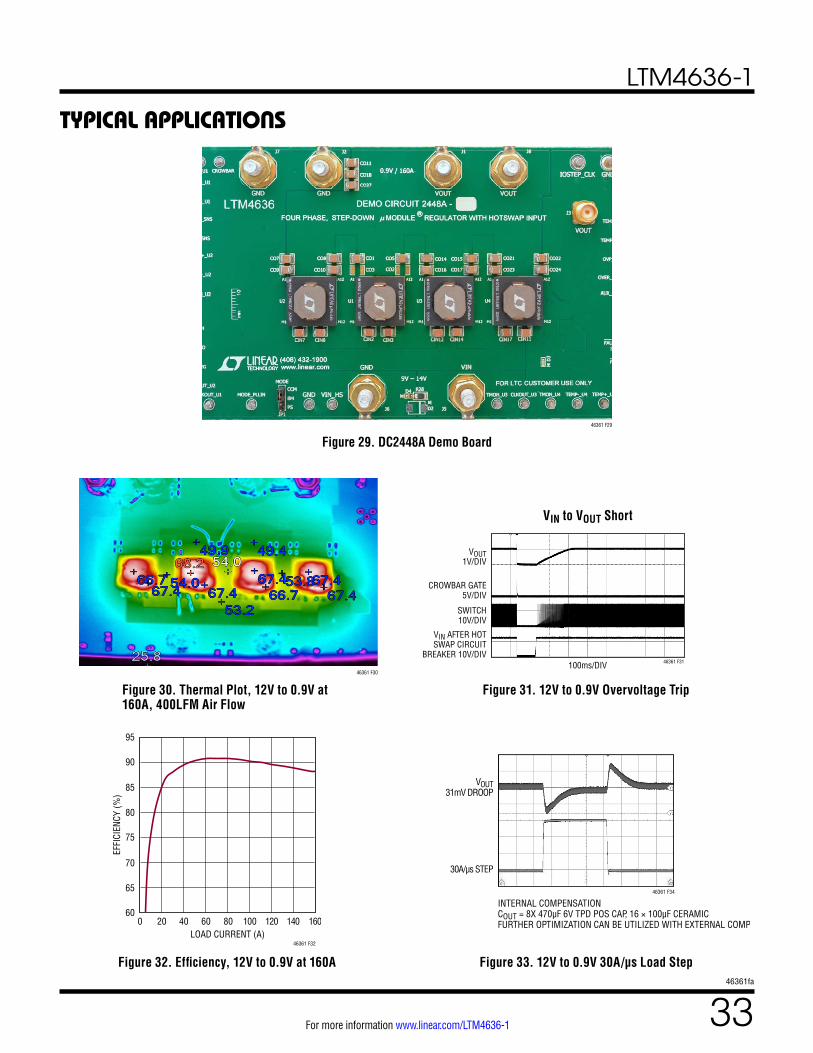
LTM4636-1
3346361fa
For more information www.linear.com/LTM4636-1
TYPICAL APPLICATIONS
Figure 29. DC2448A Demo Board
46361 F30
46361 F29
LOAD CURRENT (A)0
EFFI
CIEN
CY (%
)
95
85
75
90
80
70
65
6060 1004020 80
46361 F32
160120 140
46361 F34
VOUT31mV DROOP
30A/µs STEP
INTERNAL COMPENSATIONCOUT = 8X 470µF 6V TPD POS CAP, 16 × 100µF CERAMICFURTHER OPTIMIZATION CAN BE UTILIZED WITH EXTERNAL COMP
VIN to VOUT Short
VOUT1V/DIV
CROWBAR GATE5V/DIV
SWITCH10V/DIV
VIN AFTER HOTSWAP CIRCUIT
BREAKER 10V/DIV100ms/DIV 46361 F31
Figure 30. Thermal Plot, 12V to 0.9V at 160A, 400LFM Air Flow
Figure 31. 12V to 0.9V Overvoltage Trip
Figure 32. Efficiency, 12V to 0.9V at 160A Figure 33. 12V to 0.9V 30A/µs Load Step
LTM4636-1
3446361fa
For more information www.linear.com/LTM4636-1
PIN ID FUNCTION PIN ID FUNCTION PIN ID FUNCTION PIN ID FUNCTION PIN ID FUNCTION PIN ID FUNCTION
A1 VOUT B1 VOUT C1 VOUT D1 VOUT E1 PGOOD F1 SNSP2
A2 VOUT B2 VOUT C2 VOUT D2 VOUT E2 RUNC F2 SNSP1
A3 VOUT B3 VOUT C3 VOUT D3 VOUTS1– E3 TRACK/SS F3 HIZREG
A4 VOUT B4 VOUT C4 VOUT D4 VOUTS1+ E4 VFB F4 SGND
A5 VOUT B5 VOUT C5 VOUT D5 COMPB E5 COMPA F5 TEST2
A6 VOUT B6 VOUT C6 VOUT D6 GND E6 GND F6 INTVCC
A7 VOUT B7 VOUT C7 VOUT D7 GND E7 GND F7 GND
A8 VOUT B8 VOUT C8 VOUT D8 GND E8 GND F8 GND
A9 VOUT B9 VOUT C9 VOUT D9 GND E9 GND F9 PVCC
A10 VOUT B10 VOUT C10 VOUT D10 OVER_TEMP E10 OVP_TRIP F10 GND
A11 VOUT B11 VOUT C11 VOUT D11 VOUT E11 CROWBAR F11 OTP_SET
A12 VOUT B12 VOUT C12 VOUT D12 VOUT E12 OVP_SET F12 GND
PIN ID FUNCTION PIN ID FUNCTION PIN ID FUNCTION PIN ID FUNCTION PIN ID FUNCTION PIN ID FUNCTION
G1 GND H1 GND J1 GND K1 GND L1 GND M1 GND
G2 GND H2 TEST3 J2 GND K2 GND L2 GND M2 GND
G3 CLKOUT H3 MODE/PLLIN J3 GND K3 GND L3 GND M3 GND
G4 SGND H4 TEST1 J4 VIN K4 VIN L4 VIN M4 VIN
G5 FREQ H5 VIN J5 VIN K5 VIN L5 VIN M5 VIN
G6 GND H6 VIN J6 VIN K6 VIN L6 VIN M6 VIN
G7 PHMODE H7 PWM J7 VIN K7 VIN L7 VIN M7 VIN
G8 RUNP H8 TMON J8 GND K8 VIN L8 VIN M8 VIN
G9 BIAS H9 GMON J9 GND K9 GND L9 GND M9 GND
G10 GND H10 GND J10 GND K10 GND L10 GND M10 GND
G11 TEMP– H11 GND J11 GND K11 SW L11 SW M11 GND
G12 TEMP+ H12 GND J12 GND K12 GND L12 GND M12 GND
PACKAGE DESCRIPTION
Pin Assignment Table (Arranged by Pin Number)
PACKAGE ROW AND COLUMN LABELING MAY VARY AMONG µModule PRODUCTS. REVIEW EACH PACKAGE LAYOUT CAREFULLY.
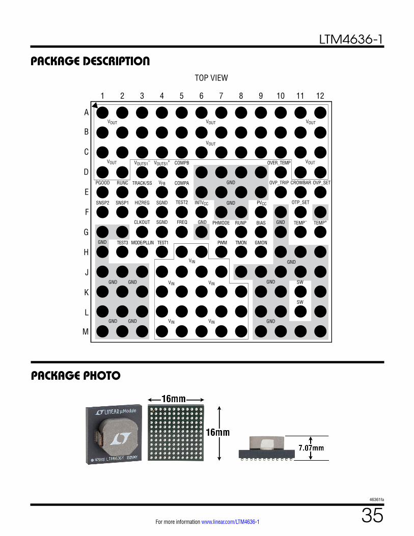
LTM4636-1
3546361fa
For more information www.linear.com/LTM4636-1
PACKAGE DESCRIPTION
VOUT
VOUT
VOUTVOUT
VOUT
VOUT
PGOOD RUNC
SNSP2 SNSP1
1 2 3 4 5 6 7
TOP VIEW
8 9 10 11 12
M
L
K
J
H
G
F
E
D
C
B
A
COMPB
TEST2
CROWBARGND
GNDINTVCC PVCC
PHMODE RUNP TEMP– TEMP+BIASCLKOUT SGND
SGND
VFB
VOUTS1+
HIZREG
TRACK/SS COMPA
VOUTS1–
FREQ
PWMTEST3 MODE/PLLIN TEST1 TMON GMON
GND
GND
GND
GND
GND
GND
GND
VIN
VIN
VIN
VIN
VINGND
GND
GND
SW
SW
OVP_TRIP OVP_SET
OTP_SET
OVER_TEMP
PACKAGE PHOTO
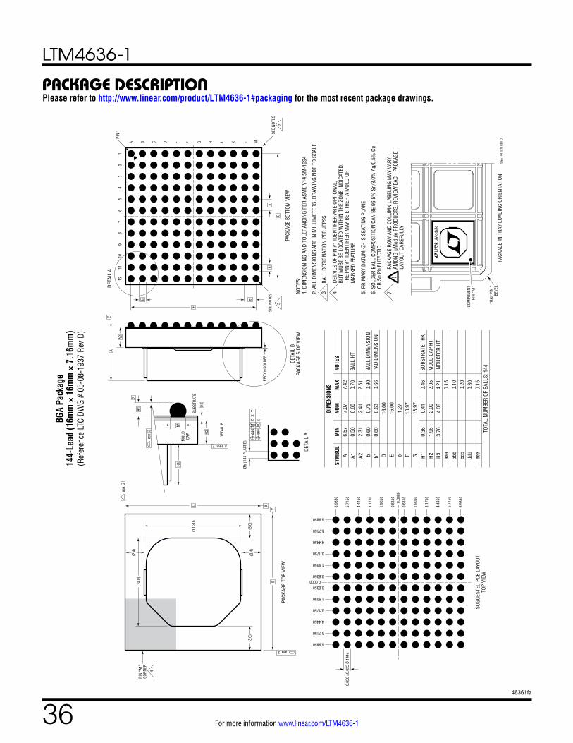
LTM4636-1
3646361fa
For more information www.linear.com/LTM4636-1
PACKAGE DESCRIPTIONPlease refer to http://www.linear.com/product/LTM4636-1#packaging for the most recent package drawings.
BGA
Pack
age
144-
Lead
(16m
m ×
16m
m ×
7.1
6mm
)(R
efer
ence
LTC
DWG
# 05
-08-
1937
Rev
D)
4
PIN
“A1”
CORN
ER
NOTE
S:1.
DIM
ENSI
ONIN
G AN
D TO
LERA
NCIN
G PE
R AS
ME
Y14.
5M-1
994
2. A
LL D
IMEN
SION
S AR
E IN
MIL
LIM
ETER
S. D
RAW
ING
NOT
TO S
CALE
BAL
L DE
SIGN
ATIO
N PE
R JE
P95
43
DETA
ILS
OF P
IN #
1 ID
ENTI
FIER
ARE
OPT
IONA
L,BU
T M
UST
BE L
OCAT
ED W
ITHI
N TH
E ZO
NE IN
DICA
TED.
THE
PIN
#1 ID
ENTI
FIER
MAY
BE
EITH
ER A
MOL
D OR
M
ARKE
D FE
ATUR
E
PACK
AGE
TOP
VIEW
X
Y
aaa
Z
aaa Z
PACK
AGE
BOTT
OM V
IEW
3
SEE
NOTE
S
SUGG
ESTE
D PC
B LA
YOUT
TOP
VIEW
BGA
144
1016
REV
D
TRAY
PIN
1BE
VEL
PACK
AGE
IN T
RAY
LOAD
ING
ORIE
NTAT
ION
COM
PONE
NTPI
N “A
1”DETA
IL A
PIN
1
0.0000
0.00
00
DETA
IL A
Øb (1
44 P
LACE
S)
D
(3.0
)(2
.4)
(2.4
)
A
DETA
IL B
PACK
AGE
SIDE
VIE
W
Z
Z
MX
YZ
ddd
MZ
eee
0.63
0 ±0
.025
Ø 1
44x
Eb
e
e
b
A2
F
G
BGA
Pack
age
144-
Lead
(16m
m ×
16m
m ×
7.0
7mm
)(R
efer
ence
LTC
DW
G #
05-0
8-19
37 R
ev D
)
0.63
50
0.63
50
1.90
50
1.90
50
3.17
50
3.17
50
4.44
50
4.44
50
5.71
50
5.71
50
6.98
50
6.9850
6.9850
5.7150
5.7150
4.4450
4.4450
3.1750
3.1750
1.9050
1.9050
0.6350
0.6350
6.98
50
GFEA B DC H MLKJ
21
43
56
712
89
1011
7
SEE
NOTE
S
DETA
IL B
SUBS
TRAT
E
A1
ccc
Z
// bbb Z
H2H1
H3 SYM
BOL
A A1 A2 b b1 D E e F G H1 H2 H3 aaa
bbb
ccc
ddd
eee
MIN
6.57
0.50
2.31
0.60
0.60
0.36
1.95
3.76
NOM
7.07
0.60
2.41
0.75
0.63
16.0
016
.00
1.27
13.9
713
.97
0.41
2.00
4.06
MAX
7.42
0.70
2.51
0.90
0.66
0.46
2.05
4.21
0.15
0.10
0.20
0.30
0.15
NOTE
S
BALL
HT
BALL
DIM
ENSI
ONPA
D DI
MEN
SION
SUBS
TRAT
E TH
KM
OLD
CAP
HTIN
DUCT
OR H
T
DIM
ENSI
ONS
TOTA
L NU
MBE
R OF
BAL
LS: 1
44
EPOX
Y/SO
LDER
(11.
20)
(10.
0)
(3.0
)
µMod
ule
5. P
RIM
ARY
DATU
M -Z
- IS
SEAT
ING
PLAN
E
6. S
OLDE
R BA
LL C
OMPO
SITI
ON C
AN B
E 96
.5%
Sn/
3.0%
Ag/
0.5%
Cu
OR
Sn
Pb E
UTEC
TIC
7PA
CKAG
E RO
W A
ND C
OLUM
N LA
BELI
NG M
AY V
ARY
AMON
G µM
odul
e PR
ODUC
TS. R
EVIE
W E
ACH
PACK
AGE
LAYO
UT C
AREF
ULLY
!
b1M
OLD
CAP
LTM4636-1
3746361fa
For more information www.linear.com/LTM4636-1
Information furnished by Linear Technology Corporation is believed to be accurate and reliable. However, no responsibility is assumed for its use. Linear Technology Corporation makes no representa-tion that the interconnection of its circuits as described herein will not infringe on existing patent rights.
REVISION HISTORYREV DATE DESCRIPTION PAGE NUMBER
A 12/17 Changed Turn-On-Time TYP from 50ms to 750µs 3
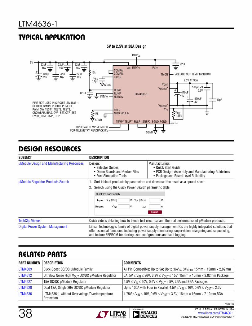
LTM4636-1
3846361fa
For more information www.linear.com/LTM4636-1 LINEAR TECHNOLOGY CORPORATION 2017
LT 1217 REV A • PRINTED IN USAwww.linear.com/LTM4636-1
RELATED PARTS
DESIGN RESOURCES
TYPICAL APPLICATION
PART NUMBER DESCRIPTION COMMENTS
LTM4609 Buck-Boost DC/DC µModule Family All Pin Compatible; Up to 5A; Up to 36VIN, 34VOUT 15mm × 15mm × 2.82mm
LTM4612 Ultralow Noise High VOUT DC/DC µModule Regulator 5A, 5V ≤ VIN ≤ 36V, 3.3V ≤ VOUT ≤ 15V, 15mm × 15mm × 2.82mm Package
LTM4627 15A DC/DC µModule Regulator 4.5V ≤ VIN ≤ 20V, 0.6V ≤ VOUT ≤ 5V, LGA and BGA Packages
LTM4620 Dual 13A, Single 26A DC/DC µModule Regulator Up to 100A with Four in Parallel, 4.5V ≤ VIN ≤ 16V, 0.6V ≤ VOUT ≤ 2.5V
LTM4636 LTM4636-1 without Overvoltage/Overtemperature Protection
4.75V ≤ VIN ≤ 15V, 0.6V ≤ VOUT ≤ 3.3V, 16mm × 16mm × 7.12mm BGA
5V to 2.5V at 30A Design
SUBJECT DESCRIPTION
µModule Design and Manufacturing Resources Design: • Selector Guides • Demo Boards and Gerber Files • Free Simulation Tools
Manufacturing: • Quick Start Guide • PCB Design, Assembly and Manufacturing Guidelines • Package and Board Level Reliability
µModule Regulator Products Search 1. Sort table of products by parameters and download the result as a spread sheet.2. Search using the Quick Power Search parametric table.
TechClip Videos Quick videos detailing how to bench test electrical and thermal performance of µModule products.
Digital Power System Management Linear Technology’s family of digital power supply management ICs are highly integrated solutions that offer essential functions, including power supply monitoring, supervision, margining and sequencing, and feature EEPROM for storing user configurations and fault logging.
COMPACOMPBTK/SS
RUNCRUNPHIZREG
FREQMODE/PLLIN
TMON
VOUT
TEMP+ TEMP– SNSP1 SNSP2 SGND
VIN
15k
47k
CSS0.1µF
22µF
2.5V AT 35A
VOLTAGE OUT TEMP MONITOR
0.1µF
22µF16V
22µF16V
22µF16V
22µF16V
22µF16V
5V
100µF25V
INTVCC
OPTIONAL TEMP MONITORFOR TELEMETRY READBACK ICs
INTVCC
INTVCC
LTM4636-1
PVCC
PGND
VOUTS1+
VOUTS1–
VFB
+
470µF4V
470µF4V
+
+
RFB1.58k
100µF ×36.3V
47pF
46361 TA02
SGND
SGND
SGND
PINS NOT USED IN CIRCUIT LTM4636-1:CLKOUT, GMON, PGOOD, PHMODE, PWM, SW, TEST1, TEST2, TEST3, CROWBAR, BIAS, OVP_SET, OTP_SET, OVER_TEMP, OVP_TRIP