LTC7106 A 7-Bit Current DAC with PMBus Interface€¦ · LTC7106 2 7106f For more information ...
24
LTC7106 1 Rev A For more information www.analog.com Document Feedback TYPICAL APPLICATION FEATURES DESCRIPTION A 7-Bit Current DAC with PMBus Interface The LTC ® 7106 is a precision, PMBus controlled, bidi- rectional current digital-to-analog converter that adjusts the output voltage of any conventional V FB referenced regulator. The LTC7106 can work with the vast majority of power management controllers or regulators to enable digital control of the output voltage. Internal power-on reset circuitry keeps the DAC output current at zero (high impedance IDAC) until a valid write takes place. Features include a range bit for easy interfacing to almost any impedance resistor divider, and an open-drain GPO output for controlling the Run or Enable pin of the DC/ DC regulator. For most applications, the current DAC error is significantly attenuated with proper design. See more detail about V OUT accuracy in the Applications Information section of this data sheet. The LTC7106 is supported by the ADI LTpowerPlay ® development tool with graphical user interface (GUI). APPLICATIONS n ±0.8% I DAC Positive Output Current Accuracy (Over Temp) n ±1.5% I DAC Negative Output Current Accuracy (Over Temp) n PMBus/I 2 C Compliant Serial Interface n Input Voltage Range: 2.5V to 5.5V n High Impedance at IDAC Output When Disabled n Wide IDAC Operation Voltage (0.4V to 2.0V) n 7-Bit Programmable DAC Output Current for DC/DC V OUT Control n Wide Range IDAC Output Current: ±16μA to ±256μA n Programmable Slew Rate: 500ns ~ 3ms per Bit n Available in a 10-Lead (3mm × 2mm) DFN Package n General Purpose Power Systems n Telecom Systems n Industrial Applications All registered trademarks and trademarks are the property of their respective owners. Margin High and Margin Low CIRCUIT OF FIGURE 11 V OUT = 24V I DAC = –40μA I DAC = 40μA I DAC = 0μA 100ms/DIV EN 2V/DIV V OUT 5V/DIV 7106 TA01b C1 1μF 10k R1 10k R2 R FB1 R FB2 C2 330μF L1 R4 10k LTC7106 V DD GND IDAC SDA SCL ALERT GPO ASEL0 ASEL1 V DD 2.5V TO 5.5V SDA ALERT SCL V DD V IN DC/DC SW V FB V OUT RUN EN (0.4V to 2V) V IN V REF 10k R3 PMBus INTERFACE –64μA TO 0μA 0μA TO 63μA 7106 TA01a
-
Upload
trinhnguyet -
Category
Documents
-
view
213 -
download
0
Transcript of LTC7106 A 7-Bit Current DAC with PMBus Interface€¦ · LTC7106 2 7106f For more information ...

LTC7106
1Rev A
For more information www.analog.comDocument Feedback
TYPICAL APPLICATION
FEATURES DESCRIPTION
A 7-Bit Current DAC with PMBus Interface
The LTC®7106 is a precision, PMBus controlled, bidi-rectional current digital-to-analog converter that adjusts the output voltage of any conventional VFB referenced regulator. The LTC7106 can work with the vast majority of power management controllers or regulators to enable digital control of the output voltage. Internal power-on reset circuitry keeps the DAC output current at zero (high impedance IDAC) until a valid write takes place. Features include a range bit for easy interfacing to almost any impedance resistor divider, and an open-drain GPO output for controlling the Run or Enable pin of the DC/DC regulator. For most applications, the current DAC error is significantly attenuated with proper design. See more detail about VOUT accuracy in the Applications Information section of this data sheet. The LTC7106 is supported by the ADI LTpowerPlay® development tool with graphical user interface (GUI).
APPLICATIONS
n ±0.8% IDAC Positive Output Current Accuracy (Over Temp)
n ±1.5% IDAC Negative Output Current Accuracy (Over Temp)
n PMBus/I2C Compliant Serial Interface n Input Voltage Range: 2.5V to 5.5V n High Impedance at IDAC Output When Disabled n Wide IDAC Operation Voltage (0.4V to 2.0V) n 7-Bit Programmable DAC Output Current for DC/DC
VOUT Control n Wide Range IDAC Output Current: ±16μA to ±256μA n Programmable Slew Rate: 500ns ~ 3ms per Bit n Available in a 10-Lead (3mm × 2mm) DFN Package
n General Purpose Power Systems n Telecom Systems n Industrial Applications
All registered trademarks and trademarks are the property of their respective owners.
Margin High and Margin Low
CIRCUIT OF FIGURE 11
VOUT = 24VIDAC = –40μA
IDAC = 40μAIDAC = 0μA
100ms/DIV
EN2V/DIV
VOUT5V/DIV
7106 TA01bC11µF
10kR1
10kR2
RFB1
RFB2
C2330µF
L1
R410k
LTC7106
VDD
GND
IDAC
SDA
SCL
ALERT
GPO
ASEL0 ASEL1
VDD2.5V
TO 5.5V
SDA
ALERT
SCL
VDD
VIN
DC/DC
SW
VFB
VOUT
RUN
EN
(0.4V to 2V)
VIN
VREF
10kR3
PMBus INTERFACE
–64μA TO 0μA
0μA TO 63μA
7106 TA01a

LTC7106
2Rev A
For more information www.analog.com
ABSOLUTE MAXIMUM RATINGS
All Pins Except GND .................................. –0.3V to 6.0VOperating Junction Temperature Range ... –40°C to 125°CStorage Temperature Range .................. –65°C to 150°C
(Note 1)
TOP VIEW
DDB PACKAGE10-LEAD (3mm × 2mm) PLASTIC DFN
θJA = 55°C/W, θJC = 16.8°C/W
SDA
SCL
VDD
ALERT
GND
ASEL1
ASEL0
GPO
EN
IDAC6
8
7
9
10
5
4
2
3
1
ORDER INFORMATIONLEAD FREE FINISH TAPE AND REEL PART MARKING* PACKAGE DESCRIPTION TEMPERATURE RANGE
LTC7106EDDB#PBF LTC7106EDDB#TRPBF LHCG 10-Lead (3mm × 2mm) Plastic DFN –40°C to 125°C
LTC7106IDDB#PBF LTC7106IDDB#TRPBF LHCG 10-Lead (3mm × 2mm) Plastic DFN –40°C to 125°C
Consult ADI Marketing for parts specified with wider operating temperature ranges. *The temperature grade is identified by a label on the shipping container.For more information on lead free part marking, go to: http://www.linear.com/leadfree/ For more information on tape and reel specifications, go to: http://www.linear.com/tapeandreel/. Some packages are available in 500 unit reels through designated sales channels with #TRMPBF suffix.
http://www.linear.com/product/LTC7106#orderinfo
PIN CONFIGURATION

LTC7106
3Rev A
For more information www.analog.com
ELECTRICAL CHARACTERISTICS The l denotes the specifications which apply over the specified operating junction temperature range, otherwise specifications are at TA = 25°C (Note 2), VDD = 3.3V, unless otherwise specified.
SYMBOL PARAMETER CONDITIONS MIN TYP MAX UNITS
VDD Power Supply 2.5 5.5 V
IQ Supply Quiescent Current EN High 700 1400 μA
ISHUTDOWN Supply Quiescent Current EN = 0V 800 μA
VUVLO_R Undervoltage Rising Threshold VDD Rising 2.35 V
VUVLO_F Undervoltage Falling Threshold VDD Falling 2.15 V
VEN_R Enable Rising Threshold VEN Rising 1.35 V
VEN_F Enable Falling Threshold VEN Falling 0.8 V
IDAC_OUT
IDAC Accuracy Full Scale Positive 0.4 ≤ VIDAC ≤ 2V (Note 3)
Range = Normal l 62.5 63 63.5 μA
Range = Low l 15.5 15.75 16.0 μA
Range = High l 246.7 252.00 255.3 μA
Full Scale Negative 0.4 ≤ VIDAC ≤ 2V (Note 3)
Range = Normal (0°C to 85°C)
–64.64 –64 –63.36 μA
Range = Normal l –64.96 –64 –63.04 μA
Range = Low l –16.36 –16 –15.64 μA
Range = High l –262.50 –256 –249.50 μA
LSB 0.4 ≤ VIDAC ≤ 2V Range = Normal 1 μA
Range = Low 0.25 μA
Range = High 4 μA
INL 0.4 ≤ VIDAC ≤ 2V Range = Normal –1 1 LSB
Range = Low –1.5 1.5 LSB
Range = High –1.6 1.6 LSB
DNL 0.4 ≤ VIDAC ≤ 2V Range = Normal –0.3 0.3 LSB
Range = Low –0.5 0.5 LSB
Range = High –0.8 0.8 LSB
IHZ High-Z Current 0.4 ≤ VIDAC ≤ 2V VEN = 0 l 20 nA
Digital Input: SDA, SCL
VIH 1.4 V
VIL 0.8 V
CPIN Input Capacitance 10 pF
Open-Drain Outputs: ALERTB, GPO, SDA
VOL Output Low Voltage ISINK = 3mA 0.4 V

LTC7106
4Rev A
For more information www.analog.com
PMBus INTERFACE TIMING CHARACTERISTICS The l denotes the specifications which apply over the specified operating junction temperature range, otherwise specifications are at TA = 25°C (Note 2), VDD = 3.3V, unless otherwise specified.
SYMBOL PARAMETER CONDITIONS MIN TYP MAX UNITS
fSCL Serial Bus Operating Frequency 10 400 kHz
tBUF Bus Free Time Between Stop and Start Condition 1.3 µs
tHD_SDA Hold Time After (Repeated) Start Condition 0.6 µs
tSU_SDA Repeated Start Condition Setup Time 0.6 µs
tSU_STO Stop Condition Setup Time 0.6 µs
tHD_DAT(OUT) Data Hold Time 300 900 ns
tHD_DAT(IN) Input Data Hold Time 0 ns
tSU_DAT Data Setup Time 100 ns
tLOW Clock Low Period 1.3 10000 µs
tHIGH Clock High Period 0.6 µs
tTIMEOUT_SMB Stuck PMBus Timer 30 ms
Note 1: Stresses beyond those listed under Absolute Maximum Ratings may cause permanent damage to the device. Exposure to any Absolute Maximum Rating condition for extended periods may affect device reliability and lifetime.Note 2: The LTC7106 is tested under pulsed load conditions such that TJ ≈ TA. The LTC7106E is guaranteed to meet performance specifications from 0°C to 85°C. Specifications over the –40°C to 125°C operating junction temperature range are assured by design, characterization and correlation with statistical process controls. The LTC7106I is guaranteed over the –40°C to 125°C operating junction temperature range. High junction temperatures degrade operating lifetimes; operating lifetime
is derated for junction temperatures greater than 125°C. Note that the maximum ambient temperature consistent with these specifications is determined by specific operating conditions in conjunction with board layout, the rated package thermal impedance and other environmental factors. TJ is calculated from the ambient temperature TA and power dissipation PD according to the following formula: TJ = TA + (PD • 55°C/W).Note 3: IDAC is a bidirectional current DAC, controlled by 2’s complementary logic. Under the setting of Range = Normal, IDAC = 63µA for Code = 0111111 provides the maximum source current and IDAC = –64µA for Code = 1000000 provides the maximum sink current. Max sink current generates the Highest VOUT, while Max source current generates the lowest VOUT. See the Operation section for more details.
TYPICAL PERFORMANCE CHARACTERISTICS
Quiescent Current vs TemperatureIDAC Leakage Current vs Temperature PIDAC Full-Scale vs Temperature
TA = 25°C, VDD = 3.3V, VIDAC = 1.0V, Range = Normal unless otherwise noted.
VEN = 0, OR VID[6:0] = 0
TEMPERATURE (°C)–50 –5 40 85 130
–1
0
1
2
3
IDAC
LEA
KAGE
(nA)
IDAC Leakage Current vs. Temp
7106 G02TEMPERATURE (°C)
–50 –10 30 70 110 15062.500
62.600
62.700
62.800
62.900
63.000
63.100
63.200
63.300
63.400
63.500
IDAC
PIDAC Full Scale VS. Temperature
7106 G03
VID[6:0] = 0111111IRANGE = NOMINAL
TEMP (°C)–50 –10 30 70 110 150
500
550
600
650
700
750
800
850
900
950
1000
I Q (μ
A)
7106 G01

LTC7106
5Rev A
For more information www.analog.com
TYPICAL PERFORMANCE CHARACTERISTICS
NIDAC vs Temperature Differential Nonlinearity Integral Nonlinearity
Buck Start-Up with IDAC Margin High and Margin Low
Boost Start-Up with IDAC Margin High and Margin Low
TA = 25°C, VDD = 3.3V, Range = Normal unless otherwise noted.
TEMPERATURE (°C)–50 0 50 100 150
–64.50
–64.40
–64.30
–64.20
–64.10
–64.00
–63.90
–63.80
–63.70
–63.60
–63.50
I DAC
(µA)
7106 G04
VID[6:0] = 1000000
CODE1 7 13 20 26 32 38 44 51 57 63
–0.30
–0.26
–0.22
–0.18
–0.14
–0.10
–0.06
–0.02
0.02
0.06
0.10
DNL
(LSB
)
7106 G05CODE
0 10 20 30 40 50 60 70–0.15
–0.12
–0.09
–0.06
–0.03
0
0.03
0.06
0.09
0.12
0.15
INL
(LSB
)
Integral Non–Linearity
7106 G06
IDAC = –60µA
IDAC = 60µA
10mV/DIV
GPO5V/DIV
VOUT0.3V/DIV
7106 G07
LTC7106 + LTM4636VOUT = 1V
IDAC = 0µA
LTC7106 + LTM4636
IDAC = –60μA
IDAC = 60μA
100ms/DIV
EN2V/DIV
VOUT200mV/DIV
7106 G08
IDAC = 0μA
VOUT = 1V
LTC7106 + LTC3784
VOUT = 24VIDAC = –40μA
IDAC = 40μAIDAC = 0μA
100ms/DIV
EN2V/DIV
VOUT5V/DIV
7106 G10
LTC7106 + LTC3784VOUT = 24VVIN = 12V
IDAC = 0μA
2ms/DIV
GPO5V/DIV
VOUT10V/DIV
7106 G09
IDAC = –40μA
IDAC = 0μA
IDAC = 40μA

LTC7106
6Rev A
For more information www.analog.com
PIN FUNCTIONSVDD (Pin 3): Input Supply. Bypass this pin to GND with a capacitor (0.1µF to 1µF).
IDAC (Pin 6): Bidirectional Current DAC Output.
EN (Pin 7): Chip Enable Pin. Current DAC output is in Hi-Z state when EN is Grounded. Do not leave EN floating.
SDA (Pin 1): Serial Bus Data Input and Open-Drain Output. A pull-up resistor to VDD is required in the application.
SCL (Pin 2): Serial Bus Clock Input.
GPO (Pin 8): Open-Drain Digital Output. A pull-up resistor to VDD is required.
ALERT (Pin 4): Open-Drain Digital Output. A pull-up resistor to VDD is required.
ASEL1/ASEL0 (Pins 10, 9): Serial Bus Address Select Inputs. Each pin has three states (VDD, FLOATING and GND); these two pins provide 9 addresses.
GND (Pin 5): Ground.

LTC7106
7Rev A
For more information www.analog.com
BLOCK DIAGRAM
+–
EN
VDD
GPO
IDAC
SDA
SCL
ALERT
ASEL0
ASEL1
VREF
GND
PMBusINTERFACE
ADDRESSADC
7-BITIDAC
VID[6:0]
R1
SLEW RATE
RANGE
7106 BD

LTC7106
8Rev A
For more information www.analog.com
OPERATIONThe LTC7106 is a PMBus controlled 7-bit D/A converter current source. Through its PMBus interface, the LTC7106 receives a 7-bit DAC code and converts this value to a bidirectional analog output current through the pin IDAC. By connecting IDAC to the feedback node of a voltage regulator, IDAC can change the output voltage of the regula-tor with the equation:
VOUT = VREF • (1 + RFB1/RFB2) – IDAC • RFB1
where VREF is the reference voltage of the voltage regula-tor. RFB1 and RFB2 are the resistor divider for the voltage regulator. IDAC is the programmed bidirectional current shown in Table 2.
A typical application diagram is shown on the front page. Therefore, the traditional pure analog designed oriented PWM controller can be controlled by a PMBus interface.
This illustrates the flexibility of the LTC7106 providing a PMBus interface to conventional analog DC/DC converters.
CHIP ENABLE (EN PIN)
The LTC7106 is activated by the EN pin. It turns on/off the device with threshold of 1.2V. When EN is low (<1.2V), IDAC is in high impedance (Hi-Z).
However, PMBus interface is still active when EN is low which means users can program the device and readback the internal register's value. The device will execute the commands of MFR_IOUT_COMMAND,
MFR_IOUT_MARGIN_HIGH, MFR_IOUT_MARGIN_LOW after EN goes high.
SLEW RATE CONTROL
To prevent abrupt changes in the D/A output current and subsequently the output voltage of the DC/DC regula-tor, an internal digital programmable slew rate control is included. The slew rate range can be programmed with a 6-bit register from 0.5µs/step to 3.58ms/step with a default value of 3.58ms/step.
CURRENT RANGE SETTING AND D/A PROGRAMMING
The LTC7106 is a 7-bit bidirectional current DAC with a 1µA LSB as its default setting. The MSB determines the current direction. When MSB is 0, IDAC is sourcing cur-rent (reducing VOUT), which is positive current flowing out of the pin, and when MSB is 1, IDAC is sinking cur-rent (increasing VOUT), which is negative current flowing into the pin. The LTC7106 also provides range high and range low options through its digital interface to change the LSB value to 4µA expanding the output current range and subsequently widening the programmable output voltage range. Alternately for higher resolution, the low range is provided with a LSB of 0.25µA. Users have ad-ditional flexibility of choosing the resistor divider ratio and resistor values to meet the output specification target. However, the design is most accurate using the nominal range which is the recommended setting. Table 1 lists the output current range and Table 2 lists the detailed DAC codes vs IDAC current.
Table 1. Output Current Range Range LSB (μA) IMIN (µA) IMAX (µA)
Nominal 1 –64 63
Range High 4 –256 252
Range Low 0.25 –16 15.75

LTC7106
9Rev A
For more information www.analog.com
DAC CODE IDAC (µA)
[6] [5] [4] [3] [2] [1] [0] NOMINALRANGE HIGH
RANGE LOW
0 0 0 0 0 0 0 0 0 0
0 0 0 0 0 0 1 1 4 0.25
0 0 0 0 0 1 0 2 8 0.5
0 0 0 0 0 1 1 3 12 0.75
0 0 0 0 1 0 0 4 16 1
0 0 0 0 1 0 1 5 20 1.25
0 0 0 0 1 1 0 6 24 1.5
0 0 0 0 1 1 1 7 28 1.75
0 0 0 1 0 0 0 8 32 2
0 0 0 1 0 0 1 9 36 2.25
0 0 0 1 0 1 0 10 40 2.5
0 0 0 1 0 1 1 11 44 2.75
0 0 0 1 1 0 0 12 48 3
0 0 0 1 1 0 1 13 52 3.25
0 0 0 1 1 1 0 14 56 3.5
0 0 0 1 1 1 1 15 60 3.75
0 0 1 0 0 0 0 16 64 4
0 0 1 0 0 0 1 17 68 4.25
0 0 1 0 0 1 0 18 72 4.5
0 0 1 0 0 1 1 19 76 4.75
0 0 1 0 1 0 0 20 80 5
0 0 1 0 1 0 1 21 84 5.25
0 0 1 0 1 1 0 22 88 5.5
0 0 1 0 1 1 1 23 92 5.75
0 0 1 1 0 0 0 24 96 6
0 0 1 1 0 0 1 25 100 6.25
0 0 1 1 0 1 0 26 104 6.5
0 0 1 1 0 1 1 27 108 6.75
0 0 1 1 1 0 0 28 112 7
0 0 1 1 1 0 1 29 116 7.25
0 0 1 1 1 1 0 30 120 7.5
0 0 1 1 1 1 1 31 124 7.75
0 1 0 0 0 0 0 32 128 8
0 1 0 0 0 0 1 33 132 8.25
0 1 0 0 0 1 0 34 136 8.5
0 1 0 0 0 1 1 35 140 8.75
0 1 0 0 1 0 0 36 144 9
0 1 0 0 1 0 1 37 148 9.25
DAC CODE IDAC (µA)
[6] [5] [4] [3] [2] [1] [0] NOMINALRANGE HIGH
RANGE LOW
0 1 0 0 1 1 0 38 152 9.5
0 1 0 0 1 1 1 39 156 9.75
0 1 0 1 0 0 0 40 160 10
0 1 0 1 0 0 1 41 164 10.25
0 1 0 1 0 1 0 42 168 10.5
0 1 0 1 0 1 1 43 172 10.75
0 1 0 1 1 0 0 44 176 11
0 1 0 1 1 0 1 45 180 11.25
0 1 0 1 1 1 0 46 184 11.5
0 1 0 1 1 1 1 47 188 11.75
0 1 1 0 0 0 0 48 192 12
0 1 1 0 0 0 1 49 196 12.25
0 1 1 0 0 1 0 50 200 12.5
0 1 1 0 0 1 1 51 204 12.75
0 1 1 0 1 0 0 52 208 13
0 1 1 0 1 0 1 53 212 13.25
0 1 1 0 1 1 0 54 216 13.5
0 1 1 0 1 1 1 55 220 13.75
0 1 1 1 0 0 0 56 224 14
0 1 1 1 0 0 1 57 228 14.25
0 1 1 1 0 1 0 58 232 14.5
0 1 1 1 0 1 1 59 236 14.75
0 1 1 1 1 0 0 60 240 15
0 1 1 1 1 0 1 61 244 15.25
0 1 1 1 1 1 0 62 248 15.5
0 1 1 1 1 1 1 63 252 15.75
1 0 0 0 0 0 0 –64 –256 –16
1 0 0 0 0 0 1 –63 –252 –15.75
1 0 0 0 0 1 0 –62 –248 –15.5
1 0 0 0 0 1 1 –61 –244 –15.25
1 0 0 0 1 0 0 –60 –240 –15
1 0 0 0 1 0 1 –59 –236 –14.75
1 0 0 0 1 1 0 –58 –232 –14.5
1 0 0 0 1 1 1 –57 –228 –14.25
1 0 0 1 0 0 0 –56 –224 –14
1 0 0 1 0 0 1 –55 –220 –13.75
1 0 0 1 0 1 0 –54 –216 –13.5
1 0 0 1 0 1 1 –53 –212 –13.25
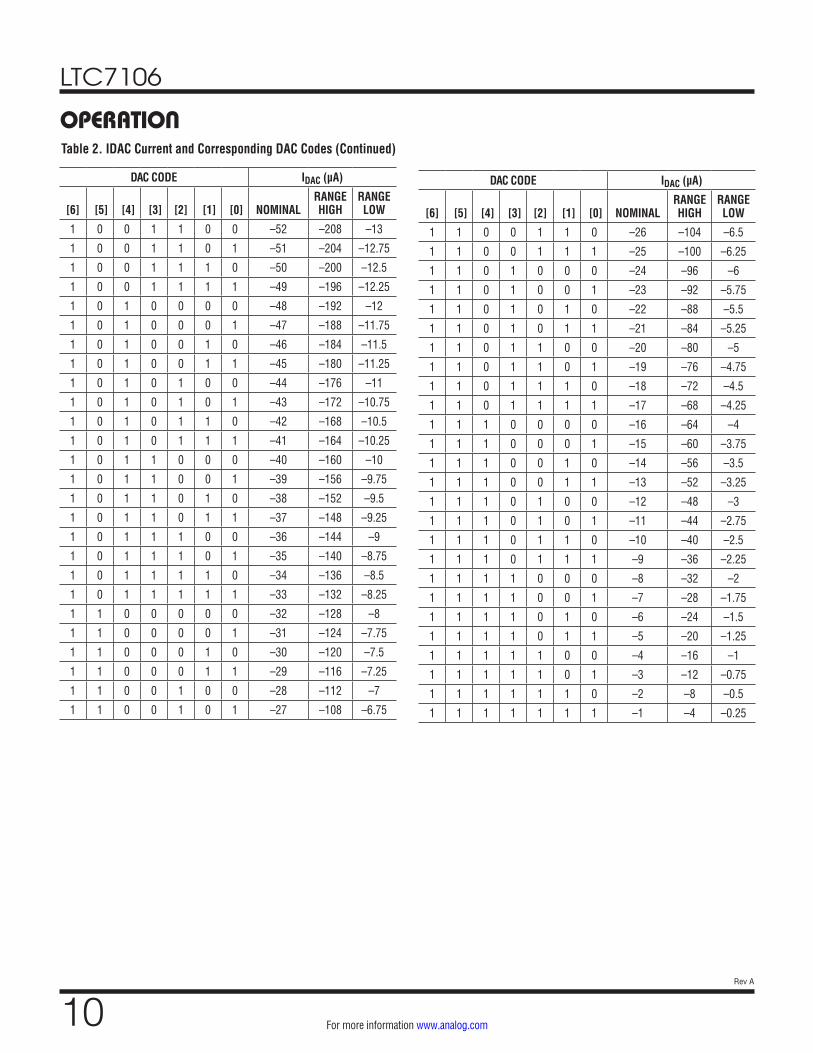
Table 2. IDAC Current and Corresponding DAC Codes
OPERATION
LTC7106
10Rev A
For more information www.analog.com
DAC CODE IDAC (µA)
[6] [5] [4] [3] [2] [1] [0] NOMINALRANGE HIGH
RANGE LOW
1 0 0 1 1 0 0 –52 –208 –13
1 0 0 1 1 0 1 –51 –204 –12.75
1 0 0 1 1 1 0 –50 –200 –12.5
1 0 0 1 1 1 1 –49 –196 –12.25
1 0 1 0 0 0 0 –48 –192 –12
1 0 1 0 0 0 1 –47 –188 –11.75
1 0 1 0 0 1 0 –46 –184 –11.5
1 0 1 0 0 1 1 –45 –180 –11.25
1 0 1 0 1 0 0 –44 –176 –11
1 0 1 0 1 0 1 –43 –172 –10.75
1 0 1 0 1 1 0 –42 –168 –10.5
1 0 1 0 1 1 1 –41 –164 –10.25
1 0 1 1 0 0 0 –40 –160 –10
1 0 1 1 0 0 1 –39 –156 –9.75
1 0 1 1 0 1 0 –38 –152 –9.5
1 0 1 1 0 1 1 –37 –148 –9.25
1 0 1 1 1 0 0 –36 –144 –9
1 0 1 1 1 0 1 –35 –140 –8.75
1 0 1 1 1 1 0 –34 –136 –8.5
1 0 1 1 1 1 1 –33 –132 –8.25
1 1 0 0 0 0 0 –32 –128 –8
1 1 0 0 0 0 1 –31 –124 –7.75
1 1 0 0 0 1 0 –30 –120 –7.5
1 1 0 0 0 1 1 –29 –116 –7.25
1 1 0 0 1 0 0 –28 –112 –7
1 1 0 0 1 0 1 –27 –108 –6.75
DAC CODE IDAC (µA)
[6] [5] [4] [3] [2] [1] [0] NOMINALRANGE HIGH
RANGE LOW
1 1 0 0 1 1 0 –26 –104 –6.5
1 1 0 0 1 1 1 –25 –100 –6.25
1 1 0 1 0 0 0 –24 –96 –6
1 1 0 1 0 0 1 –23 –92 –5.75
1 1 0 1 0 1 0 –22 –88 –5.5
1 1 0 1 0 1 1 –21 –84 –5.25
1 1 0 1 1 0 0 –20 –80 –5
1 1 0 1 1 0 1 –19 –76 –4.75
1 1 0 1 1 1 0 –18 –72 –4.5
1 1 0 1 1 1 1 –17 –68 –4.25
1 1 1 0 0 0 0 –16 –64 –4
1 1 1 0 0 0 1 –15 –60 –3.75
1 1 1 0 0 1 0 –14 –56 –3.5
1 1 1 0 0 1 1 –13 –52 –3.25
1 1 1 0 1 0 0 –12 –48 –3
1 1 1 0 1 0 1 –11 –44 –2.75
1 1 1 0 1 1 0 –10 –40 –2.5
1 1 1 0 1 1 1 –9 –36 –2.25
1 1 1 1 0 0 0 –8 –32 –2
1 1 1 1 0 0 1 –7 –28 –1.75
1 1 1 1 0 1 0 –6 –24 –1.5
1 1 1 1 0 1 1 –5 –20 –1.25
1 1 1 1 1 0 0 –4 –16 –1
1 1 1 1 1 0 1 –3 –12 –0.75
1 1 1 1 1 1 0 –2 –8 –0.5
1 1 1 1 1 1 1 –1 –4 –0.25
OPERATIONTable 2. IDAC Current and Corresponding DAC Codes (Continued)
LTC7106
11Rev A
For more information www.analog.com
OPERATIONGPO
GPO is a general purpose open-drain output pin, which can be set by PMBus command. It is designed to turn on/off the DC/DC regulator by connecting GPO to the RUN pin of the regulator. Once GPO is set high, it stays high even if the EN pin goes low as long as the device is not power cycled.
ADDRESS
The PMBus address is selected by ASEL0 and ASEL1 pins. Each pin has three states: high, low and floating. The possible PMBus addresses are shown in Table 3.
Table 3. Address SelectionASEL1 ASEL0 PMBus ADDRESS
GND GND 2A
GND VDD 2C
GND FLOAT 2E
VDD GND 4A
VDD VDD 4C
VDD FLOAT 4E
FLOAT GND 6A
FLOAT VDD 6C
FLOAT FLOAT 6E
PMBus SERIAL INTERFACE
The LTC7106 serial interface is a PMBus-compliant slave device and can operate at any frequency between 10kHz and 400kHz. In addition the LTC7106 always responds to the global broadcast address of 0x5A or 0x5B (7-bit). The serial interface supports the following protocols defined in the PMBus specifications: 1) send command, 2) write byte, 3) group, 4) read byte and 5) read word. The PMBus write operations are not acted upon until a complete valid message is received by the LTC7106 including the STOP bit.
Communication Failure
Attempts to access unsupported commands or writing invalid data to supported commands will result in a CML fault. The CML bit is set in the STATUS_BYTE command and the ALERT pin is pulled low.
Device Addressing
The LTC7106 offers four different types of addressing over the PMBus interface, specifically: 1) global, 2) device, 3) rail addressing and 4) alert response address (ARA).
Global addressing provides a means of the PMBus master to address all LTC7106 devices on the bus. The LTC7106 global addresses are fixed 0x5A or 0x5B (7 bit) or 0xB4 or 0xB6 (8 bit) and cannot be disabled.
Device addressing provides the standard means of the PMBus master communicating with a single instance of a LTC7106. The value of the device address is set by the ASEL0/ASEL1 configuration pins. Rail addressing provides a means of the PMBus master addressing a set of channels connected to the same output rail, simul-taneously. This is similar to global addressing, however, the PMBus address can be dynamically assigned by using the MFR_RAIL_ADDRESS command. It is recom-mended that rail addressing should be limited to command write operations.
All four means of PMBus addressing require the user to employ disciplined planning to avoid addressing conflicts.
Fault Status
The STATUS_BYTE and ALERT pin provide fault status information of the LTC7106 to the host.
Bus Timeout Failure
The LTC7106 implements a timeout feature to avoid hang-ing the serial interface. The data packet timer begins at the first START event before the device address write byte. Data packet information must be completed within 25ms or the LTC7106 will tri-state the bus and ignore the given data packet. Data packet information includes the device address byte write, command byte, repeat start event (if a read operation), device address byte read (if a read operation), and all data bytes.
The user is encouraged to use as high a clock rate as possible to maintain efficient data packet transfer be-tween all devices sharing the serial bus interface. The LTC7106 supports the full PMBus frequency range from 10kHz to 400kHz.
LTC7106
12Rev A
For more information www.analog.com
OPERATIONSimilarity Between PMBus, SMBus and I2C 2-Wire Interface
The PMBus 2-wire interface is an incremental extension of the SMBus. SMBus is built upon I2C with some minor differences in timing, DC parameters and protocol. The PMBus/SMBus protocols are more robust than simple I2C byte commands because PMBus/SMBus provide timeouts to prevent bus hangs and valid operation commands. In general, a master device that can be configured for I2C communication can be used for PMBus communication with little or no change to hardware or firmware. Repeat start (restart) is not supported by all I2C controllers but is required for SMBus/PMBus reads. If a general purpose I2C controller is used, check that repeat start is supported.
For a description of the minor extensions and exceptions PMBus makes to SMBus, refer to PMBus Specification Part 1, Revision 1.1: Paragraph 5: Transport.
For a description of the differences between SMBus and I2C, refer to System Management Bus (SMBus) Specification Version 2.0: Appendix B—Differences Between SMBus and I2C.
PMBus SERIAL INTERFACE
The LTC7106 communicates with a host (master) using the standard PMBus serial bus interface. The Timing Diagram, Figure 1, shows the timing relationship of the signals on the bus. The two-bus lines, SDA and SCL, must be high when the bus is not in use. External pull-up resistors or current sources are required on these lines.
The LTC7106 is a slave device. The master can com-municate with the LTC7106 using the following formats:
• Master Transmitter, Slave Receiver
• Master Receiver, Slave Transmitter
The following PMBus protocols are supported:
• Write Byte, Send Byte
• Read Byte, Read Word
• Alert Response Address
Figure 3 through Figure 6 illustrate the aforementioned PMBus protocols. All transactions support GCP (group command protocol).
Figure 2 is a key to the protocol diagrams in this section.
A value shown below a field in the following figures is a mandatory value for that field.
The data formats implemented by PMBus are:
• Master transmitter transmits to slave receiver. The transfer direction in this case is not changed.
• Master reads slave immediately after the first byte. At the moment of the first acknowledgment (provided by the slave receiver) the master transmitter becomes a master receiver and the slave receiver becomes a slave transmitter.
• Combined format. During a change of direction within a transfer, the master repeats both a start condition and the slave address but with the R/W bit reversed. In this case, the master receiver terminates the transfer by generating a NACK on the last byte of the transfer and a STOP condition.
Examples of these formats are shown in Figure 4 and Figure 5.

LTC7106
13Rev A
For more information www.analog.com
Figure 1. Timing Diagram
OPERATION
SDA
SCL
tHD(STA)tHD(DAT)
tSU(STA) tSU(STO)
tSU(DAT)tLOW
tHD(SDA) tSP tBUF
STARTCONDITION
STOPCONDITION
REPEATED STARTCONDITION
STARTCONDITION
trtf
trtf
tHIGH 7106 F01
SLAVE ADDRESS DATA BYTEWr A A P
7106 F02
S
7
S START CONDITION
Sr REPEATED START CONDITION
Rd READ (BIT VALUE OF 1)
Wr WRITE (BIT VALUE OF 0)
x SHOWN UNDER A FIELD INDICATES THAT THAT FIELD IS REQUIRED TO HAVE THE VALUE OF x
A ACKNOWLEDGE (THIS BIT POSITION MAY BE 0 FOR AN ACK OR 1 FOR A NACK)
P STOP CONDITION
PEC PACKET ERROR CODE
MASTER TO SLAVE
SLAVE TO MASTER
CONTINUATION OF PROTOCOL
81 1 1
x x
11
...
SLAVE ADDRESS COMMAND CODE DATA BYTEWr A A A P7106 F03
S
7 8 81 1 1 1 11
SLAVE ADDRESS Wr A A P7106 F04
S
7 81 1 1 11
COMMAND CODE
SLAVE ADDRESS COMMAND CODE SLAVE ADDRESSWr A A A P
7106 F05
S
7 8 7 1
DATA BYTE LOW
8
DATA BYTE HIGH
811 1 1
Sr
1 1
1
11
A
1
Rd A
SLAVE ADDRESS COMMAND CODE SLAVE ADDRESSWr A A Sr P
7106 F06
S
7 8 8 11
DATA BYTE
8 1
1
1 1 1 11 1
ARd A
Figure 2. PMBus Packet Protocol Diagram Element Key
Figure 3. Write Byte Protocol
Figure 4. Send Byte Protocol
Figure 5. Read Word Protocol
Figure 6. Read Byte Protocol

LTC7106
14Rev A
For more information www.analog.com
Table 4. LTC7106 Supported PMBus CommandsPMBus CODE
(8 BITS) R/W TYPE COMMAND NAME DESCRIPTION
0x01 R/W OPERATION Default is On: [7:0] = 0x80
0x78 R/W STATUS_BYTE Read Fault Status: CML, Write 1 to Reset
0x98 Read PMBUS_REVISION Read PMBus Revision = 0x22 for Rev 1.2
0xE2 R/W MFR_CHIP_CTRL [7:4] – Reserved: [7:0] = 0x00 Default [0] = GPO EN, [1] = Reserved, [2] = Write Protect, [3] = Timeout Status
0xE4 R/W MFR_DAC_CTRL [7:6] = Current Step Control, [5:0] = DAC Slew Rate Control
0xE5 R/W MFR_IOUT_MARGIN_HIGH Same Format as MFR_IOUT_COMMAND
0xE6 R/W MFR_IOUT_MAX Clamped Value that DAC Cannot Exceed. Default 7-Bit Value of 0x00 = Source Current Only
0xE7 Read MFR_SPECIAL_ID MFR Special ID for LTC7106 = 0x8080
0xE8 R/W MFR_IOUT_COMMAND IOUT Margining Command (see Table 5) [5:0] Step Value, Source: [6] = 0, Sink: [6] = 1
0xED R/W MFR_IOUT_MARGIN LOW Same Format as MFR_IOUT_COMMAND
0xFA R/W MFR_RAIL_ADDRESS Set Common PMBus Address [6:0], [7] = 0 Enable, [7] = 1 Disable
0xFD Write MFR_RESET Reset PMBus Interface to Power-On State Write Data is Ignored; 0, 1, 2 Bytes
REGISTER COMMAND DETAILS
MFR_IOUT_COMMAND
The DAC output current command is formatted as a 7-bit 2’s complement value. When the operation register is set to 0x80, DAC takes the value stored in this register. Setting bit[6] to 0 sources the current from the IC and bit[6] to 1 sinks the current into the IC. Default value for this register is 0x00. The valid range of values are from 0x40 to 0x3F.
Do not attempt to write values outside of this range or undesired behavior may result. Writes to this register are inhibited when the WPB, bit [2] in MFR_CHIP_CTRL, is set high.
MFR_IOUT_MARGIN_HIGH
DAC margining register with the same format and rules as MFR_IOUT_COMMAND. The DAC value will take the value stored in this register when the operation register is set to margin high, 0xA8.
MFR_IOUT_MARGIN_LOW
DAC margining register with the same format and rules as MFR_IOUT_COMMAND. The DAC value will take the value stored in this register when the operation register is set to margin low, 0x98.
MFR_IOUT_MAX
Clamping value that DAC cannot exceed. The format is a 7-bit 2’s complement value, the same as the margin registers. Therefore, the DAC value cannot be a smaller 2’s complement value than what is stored in this register.
The 7-bit default value is 0x00 = cannot sink current. IOUT cannot be set to a higher value unless this value is changed to a negative number, bit [7] = 1.
Setting this register to 0x40 allows the LTC7106 to sink the maximum current with no clamping.

LTC7106
15Rev A
For more information www.analog.com
REGISTER COMMAND DETAILS MFR_CHIP_CTRL
This register is for general chip control and status. Please refer to Table 7 for each bit description.
Bits Description
[7:4] Reserved
[3] Timeout Status:
0 = No PMBus Timeout Occurred
1 = A Timeout Occurred
Writing a 1 to this bit will clear this bit
[2] Write Protect for Margin Registers
0 = Write Allowed
1 = Writes Inhibited
[1] Reserved
[0] GPO, General Purpose Output
0 = GPO Pulls Open Drain to GND
1 = Hi-Z on GPO
MFR_DAC_CTRL
8-bit register to control the IDAC LSB current value and the timer count for the slew rate control. Default value = 0x40.
Bits Description
[7:6] Selector Range for IDAC Step Current: b’00 = 0.25µA/Step, Range Low b’01 = 1.0µA/Step, Nominal b’10 = 4.0µA/Step, Range High b’11 = Reserved
[5:0] Selector for Time in µs/Step Default Value 0x00 = Max = 3584µs/Step See Table 6 for Allowable Values
Only a power cycle, POR, will reset this register to prevent unwanted immediate current changes in IDAC. MFR_RESET will not reset this register.
In addition, IDAC must be at 0x00 to change the current range selector to prevent unwanted large swings in IDAC current. The time step selector, bits [5:0], can be changed at any time.Table 5. Programmable Delay Per Current Step
Slew Rate Timer Clock (µs/Step)[5:0] [5:0] [5:0]
0 0 0 0 0 0 = 3584 0 1 0 0 0 0 = 16 1 0 0 0 0 0 = 256
0 0 0 0 0 1 = 0.5 0 1 0 0 0 1 = 20 1 0 0 0 0 1 = 320
0 0 0 0 1 0 = 1.0 0 1 0 0 1 0 = 24 1 0 0 0 1 0 = 384
0 0 0 0 1 1 = 1.5 0 1 0 0 1 1 = 28 1 0 0 0 1 1 = 448
0 0 0 1 0 0 = 2.0 0 1 0 1 0 0 = 32 1 0 0 1 0 0 = 512
0 0 0 1 0 1 = 2.5 0 1 0 1 0 1 = 40 1 0 0 1 0 1 = 640
0 0 0 1 1 0 = 3.0 0 1 0 1 1 0 = 48 1 0 0 1 1 0 = 768
0 0 0 1 1 1 = 3.5 0 1 0 1 1 1 = 56 1 0 0 1 1 1 = 896
0 0 1 0 0 0 = 4.0 0 1 1 0 0 0 = 64 1 0 1 0 0 0 = 1280*
0 0 1 0 0 1 = 5.0 0 1 1 0 0 1 = 80 1 0 1 0 0 1 = 1280
0 0 1 0 1 0 = 6.0 0 1 1 0 1 0 = 96 1 0 1 0 1 0 = 1536
0 0 1 0 1 1 = 7.0 0 1 1 0 1 1 = 112 1 0 1 0 1 1 = 1792
0 0 1 1 0 0 = 8.0 0 1 1 1 0 0 = 128 1 0 1 1 0 0 = 2560*
0 0 1 1 0 1 = 10 0 1 1 1 0 1 = 160 1 0 1 1 0 1 = 2560
0 0 1 1 1 0 = 12 0 1 1 1 1 0 = 192 1 0 1 1 1 0 = 3584*
0 0 1 1 1 1 = 14 0 1 1 1 1 1 = 224 1 0 1 1 1 1 = 3584
* Duplicate Encoding

LTC7106
16Rev A
For more information www.analog.com
Figure 7. MFR_RAIL_ADDRESS Data Byte
PMBus COMMAND DETAILS
7106 F07
B7 B0
7-BIT ADDRESSDISA
BLE
CLEAR B7 TO ENABLE RAIL ADDRESS
MFR_RESET
This command provides a means by which the user can perform a reset of the LTC7106. All latched faults (ALERT and status register) and register contents will be reset to a power-on condition by this command. VOUT will remain in regulation but may change due to the reset of the margin registers.
This write-only command accepts zero, one, or two data bytes but ignores them.
MFR_RAIL_ADDRESS
The MFR_RAIL_ADDRESS command allows all devices to share a common address, such as all devices attached to a single power supply rail. The desired 7-bit address value is written to the 7 bits of the data byte.
The MSB (bit B7) must be set low to enable communication using the MFR_RAIL_ADDRESS address. Setting this bit disables this address. The default for this register is 0x80.
OPERATION
The OPERATION command is used to turn the unit on/off and for margining the output voltage.
The ON bit is automatically reset to ON after a master shutdown (EN), power cycle, or MFR_RESET command.
The MARGIN_LOW/HIGH bits command the IOUT refer-ence to the offset value stored in either the MFR_IOUT_MARGIN_HIGH or MFR_IOUT_MARGIN_LOW.
This command has one data byte. It will accept one or two but ignores the second byte.
Table 6. Supported OPERATION Command Register ValuesACTION VALUE
Turn Off Immediately 0x00
Turn On 0x80
Margin Low 0x98
Margin High 0xA8
PMBus_REVISION
The PMBUS_REVISION command indicates the revision of the PMBus to which the device is compliant. The LTC7106 is PMBus Version 1.2 compliant in both Part I and Part II.
This read-only command has one data byte and will return 0x22.
MFR_SPECIAL_ID
The 16-bit word representing a unique identification for LTpowerPlay.
This read-only command has 2 data bytes and is set to 0x8080.
The user should only perform command writes to this address. If a read is performed from this address and the rail devices do not respond with EXACTLY the same value, the LTC7106 will detect bus contention and abort its read command with no CML or ALERTB set.
This command accepts one or two data bytes but the second is ignored.
LTC7106
17Rev A
For more information www.analog.com
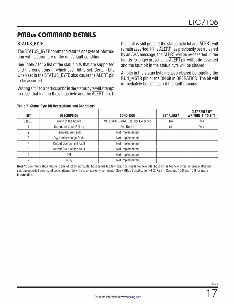
STATUS_BYTE
The STATUS_BYTE command returns one byte of informa-tion with a summary of the unit’s fault condition.
See Table 7 for a list of the status bits that are supported and the conditions in which each bit is set. Certain bits when set in the STATUS_BYTE also cause the ALERT pin to be asserted.
Writing a “1” to a particular bit in the status byte will attempt to reset that fault in the status byte and the ALERT pin. If
PMBus COMMAND DETAILSthe fault is still present the status byte bit and ALERT will remain asserted. If the ALERT has previously been cleared by an ARA message, the ALERT will be re-asserted. If the fault is no longer present, the ALERT pin will be de-asserted and the fault bit in the status byte will be cleared.
All bits in the status byte are also cleared by toggling the RUN_MSTR pin or the ON bit in OPERATION. The bit will immediately be set again if the fault remains.
Table 7. Status Byte Bit Descriptions and Conditions
BIT DESCRIPTION CONDITION SET ALERT?CLEARABLE BY
WRITING ‘1’ TO BIT?
0 (LSB) None of the Above MFR_VOUT_MAX Register Exceeded No Yes
1 Communication Failure (See Note 1) Yes Yes
2 Temperature Fault Not Implemented
3 VIN Undervoltage Fault Not Implemented
4 Output Overcurrent Fault Not Implemented
5 Output Overvoltage Fault Not Implemented
6 OFF Not Implemented
7 Busy Not Implemented
Note 1: Communication failure is one of following faults: host sends too few bits, host reads too few bits, host writes too few bytes, improper R/W bit set, unsupported command code, attempt to write to a read-only command. See PMBus Specification v1.2, Part II, Sections 10.8 and 10.9 for more information.

LTC7106
18Rev A
For more information www.analog.com
IDAC ACCURACY
The LTC7106 provides three ranges of IDAC output current. However, only nominal range (LSB = ±1µA) is optimized with the highest accuracy. It is recommended that users design the resistor divider using the nominal range of the IDAC setting.
TWO’S COMPLEMENTARY CODE
VID [6:0] of the LTC7106 is in the format of two’s comple-mentary. From Table 2, it is easy to program the register once the desired output current is known. For example, if output current is 20µA, then set VID [6:0] = 0010100. If the output current is –20µA, then set VID [6:0] = 1101100 for the nominal IDAC setting.
VOUT ACCURACY
When IDAC = 0, define:
VOUT0 = VREF 1+ RFB1
RFB2
⎡⎣⎢
⎤⎦⎥
(1)
Referring to Figure 8, the output voltage is set according to:
VOUT = VREF 1+ RFB1
RFB2
⎡⎣⎢
⎤⎦⎥
–IDAC • RFB1
(2)
APPLICATIONS INFORMATIONDefine ∆VOUT as the VOUT error caused by the IDAC error ∆IDAC, then we can derive the following equation from equation (1) and (2):
∆VOUTVOUT
= ∆IDAC / IDACRatio – 1
⎛⎝⎜
⎞⎠⎟
(3)
Where:
Ratio =
VOUT0
IDAC • RFB1 (4)
It is clear that when Ratio < 0 or Ratio ≥ 2, the VOUT error can be attenuated from the IDAC error:
|
∆VOUT
VOUT| ≤ |
∆IDAC
IDAC|
(5)
In the case of margin high, IDAC < 0 so Ratio < 0. Therefore, the VOUT error is always smaller than the IDAC error by a factor of:
VOUT0
IDAC • RFB1– 1
(6)
In the case of margin low, IDAC > 0. So the VOUT error will only be attenuated when:
Ratio =VOUT0
IDAC • RFB1> 2
or IDAC • RFB1 <VOUT0
2 (7)
In other words, as long as VOUT is margining low within 50% of the VOUT default value, VOUT0, the VOUT error won't be larger than the IDAC error.
DESIGN EXAMPLES
The LTC7106 can work with almost all the power manage-ment controllers or regulators. Figure 9, Figure 10 and Figure 11 show three design examples using the LTC7106 to control the output voltage with a monolithic buck regu-lator, an μModule® and a boost controller.
RFB1
RFB2
VOUT
IDAC
VREF LTC7106
7106 F08
Figure 8. Setting the Output Voltage Using the LTC7106

LTC7106
19Rev A
For more information www.analog.com
Case One
Assume that the LTC7150S, a monolithic buck regula-tor, provides a 1.5V output and requires to margin low VOUT from 1.5V to 1.0V (see Figure 9). The VFB is 0.6V and the voltage dividers are external. In order to achieve the best accuracy of the LTC7106, it is recommended to design IDAC in nominal range. Also within certain current range (nominal, high or low), the larger the absolute IDAC
current amplitude is, the better accuracy the LTC7106 can achieve. So it is easy to choose RTOP = 10kΩ and RBOT = 6.65kΩ. Then IDAC = (1.5V – 1.0V)/10kΩ = + 50μA. Choose MFR_CONTROL [6:5] = 00 (Range = Nominal) to set IDAC LSB =1μA.
By looking in Table 2, choose DAC [6:0] = 0110010 to set the IDAC = +50μA, which will margin VOUT from 1.5V to 1.0V.
Figure 9. Using the LTC7106 to Margin Low Monolithic Buck Regulator LTC7150S Providing 1.5V to 1.0V at 20A
APPLICATIONS INFORMATION
GPO
VOUT
1µF10k10k10k
330µF
0.25µH
22pF
4.7μF
LTC7106
VDD
GND
SDA
SCL
ALERT
GPOASEL0 ASEL1
VDD2.5V TO 5.5V
SDA
ALERT
SCL
+50µA
EN
LTC7150S
PGOOD
INTVCC
RUN
TRACK/SS
ITH
SW
FB
VOUT–
MODE/SYNC
SGND
RT
1.5V/20A
6.65k
10k+100µF
×2
TO MARGIN LOW VOUT FROM 1.5V TO 1V
PVIN
SVIN
PHMODE
CLKOUT
10k
10k162k
1nF
VIN3.1V TO 20V
22µF×2
IDAC
7106 F09
PMBus INTERFACE
10k
LTC7106
20Rev A
For more information www.analog.com
APPLICATIONS INFORMATION
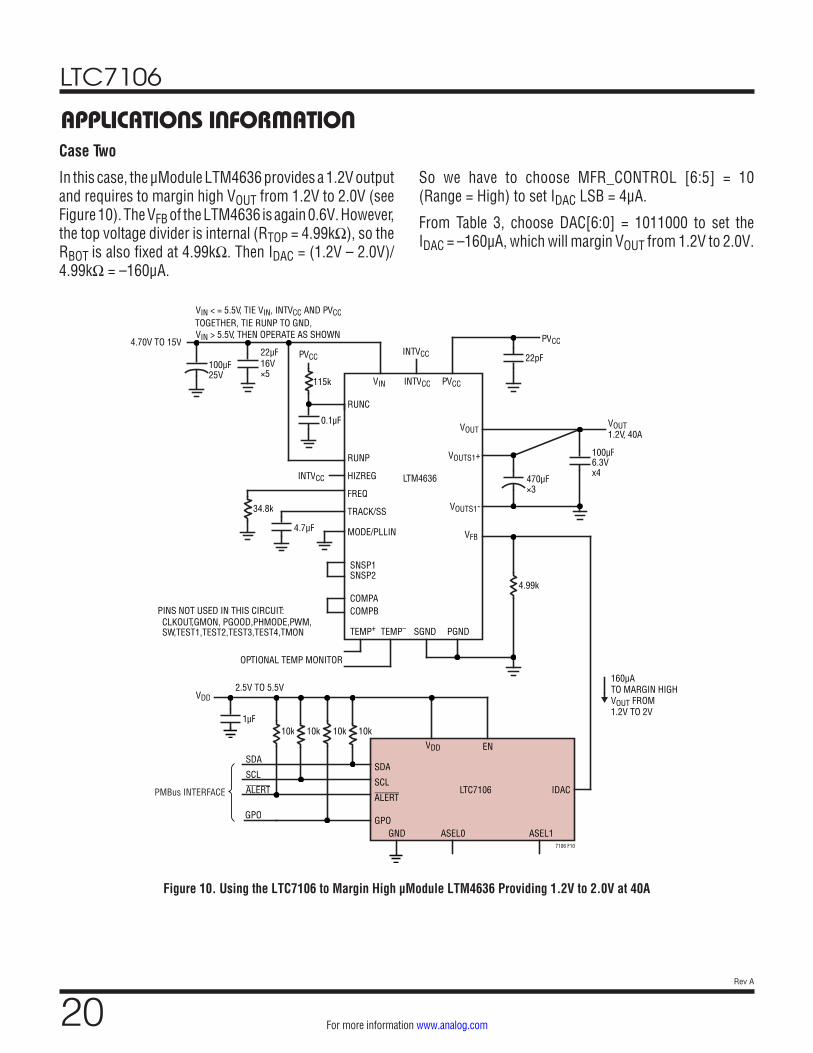
Figure 10. Using the LTC7106 to Margin High μModule LTM4636 Providing 1.2V to 2.0V at 40A
Case Two
In this case, the μModule LTM4636 provides a 1.2V output and requires to margin high VOUT from 1.2V to 2.0V (see Figure 10). The VFB of the LTM4636 is again 0.6V. However, the top voltage divider is internal (RTOP = 4.99kΩ), so the RBOT is also fixed at 4.99kΩ. Then IDAC = (1.2V – 2.0V)/4.99kΩ = –160μA.
So we have to choose MFR_CONTROL [6:5] = 10 (Range = High) to set IDAC LSB = 4μA.
From Table 3, choose DAC[6:0] = 1011000 to set the IDAC = –160µA, which will margin VOUT from 1.2V to 2.0V.
GPO
1µF10k10k10k
22pF
115k
100µF22µF
0.1µF
34.8k
4.7µF
470µF
4.99k
100µF
LTC7106
VDD
GND
SDA
SCL
ALERT
GPOASEL0 ASEL1
VDD2.5V TO 5.5V
SDA
ALERT
SCL
EN
LTM4636
RUNC
RUNP
HIZREG
FREQ
MODE/PLLIN
SNSP1
PVCC
TRACK/SS
VOUT
VOUTS1+
VOUTS1-
VFB
SNSP2
COMPACOMPB
VIN INTVCC PVCC25V
4.70V TO 15V
16V×5
PVCC
INTVCC
INTVCC
×3
SGND PGNDTEMP+ TEMP–
OPTIONAL TEMP MONITOR
PINS NOT USED IN THIS CIRCUIT:CLKOUT,GMON, PGOOD,PHMODE,PWM,SW,TEST1,TEST2,TEST3,TEST4,TMON
6.3Vx4
VOUT1.2V, 40A
VIN < = 5.5V, TIE VIN, INTVCC AND PVCCTOGETHER, TIE RUNP TO GND,VIN > 5.5V, THEN OPERATE AS SHOWN
IDAC
160μATO MARGIN HIGH VOUT FROM 1.2V TO 2V
10k
7106 F10
PMBus INTERFACE

LTC7106
21Rev A
For more information www.analog.com
Figure 11. Using the LTC7106 with a Boost Controller to Vary VOUT from 28V to 18V
APPLICATIONS INFORMATIONCase Three
The LTC7106 can also work with boost converters. In this case, the LTC3784, a synchronous boost controller, provides a 2-phase 28V/10A output and requires to control VOUT from 28V to 18V (see Figure 11). The VFB is 1.2V and the voltage dividers are external. Based on the same
design criteria in Case One, we can choose RTOP = 200kΩ and RBOT = 8.97kΩ for the best accuracy. Then IDAC = (28V – 18V)/200kΩ = +50µA. Choose MFR_CONTROL [6:5] = 00 (Range Nominal) to set IDAC LSB = 1µA. By looking in Table 2, choose DAC[6:0] = 0001110 to set the IDAC = +50μA, which will margin VOUT from 28V to 18V.
0.1µF
GPO
INTVCC
1µF10k10k10k
LTC7106
VDD
GND
SDA
SCL
ALERT
GPOASEL0 ASEL1
VDD2.5V TO 5.5V
SDA
ALERT
SCL
EN
LTC3784
PGOOD
FREQ
OVMODE
VBIAS
MODE/PLLIN
ITH
SENSE1–
SENSE1+
TG1
SW1
INTVCC
SGNDSS PGND
+50µATO MARGIN LOW VOUT FROM 28V TO 18V
100pF
15nF
8.66k0.1µF
100k
47µF
VBATT
12VDOWN TO 2.3V AFTERSTART-UP IF VBIAS ISPOWERED FROM VOUT
BG1
BOOST1
SENSE2–SENSE2+
SW2
BG2
BOOST2
TG2
VFB
4.7µF
4mΩ
0.1µF
200k
3.3μH
4mΩ 3.3μH
VOUT28V AT 10A
220µF
8.97k
IDAC
7106 F11
PMBus INTERFACE
10k

LTC7106
22Rev A
For more information www.analog.com
PACKAGE DESCRIPTIONPlease refer to http://www.linear.com/product/LTC7106#packaging for the most recent package drawings.
2.00 ±0.10(2 SIDES)
NOTE:1. DRAWING CONFORMS TO VERSION (WECD-1) IN JEDEC PACKAGE OUTLINE M0-229 2. DRAWING NOT TO SCALE 3. ALL DIMENSIONS ARE IN MILLIMETERS4. DIMENSIONS OF EXPOSED PAD ON BOTTOM OF PACKAGE DO NOT INCLUDE MOLD FLASH. MOLD FLASH, IF PRESENT, SHALL NOT EXCEED 0.15mm ON ANY SIDE5. EXPOSED PAD SHALL BE SOLDER PLATED6. SHADED AREA IS ONLY A REFERENCE FOR PIN 1 LOCATION ON THE TOP AND BOTTOM OF PACKAGE
0.40 ±0.10
BOTTOM VIEW—EXPOSED PAD
0.64 ±0.05(2 SIDES)
0.75 ±0.05
R = 0.115TYPR = 0.05
TYP
2.39 ±0.05(2 SIDES)
3.00 ±0.10(2 SIDES)
15
106
PIN 1 BARTOP MARK
(SEE NOTE 6)
0.200 REF
0 – 0.05
(DDB10) DFN 0905 REV Ø
0.25 ±0.050.50 BSC
PIN 1R = 0.20 OR0.25 × 45°CHAMFER
0.25 ±0.05
2.39 ±0.05(2 SIDES)
RECOMMENDED SOLDER PAD PITCH AND DIMENSIONS
0.64 ±0.05(2 SIDES)
1.15 ±0.05
0.70 ±0.05
2.55 ±0.05
PACKAGEOUTLINE
0.50 BSC
DDB Package10-Lead Plastic DFN (3mm × 2mm)
(Reference LTC DWG # 05-08-1722 Rev Ø)

LTC7106
23Rev A
For more information www.analog.com
REVISION HISTORYREV DATE DESCRIPTION PAGE NUMBER
A 04/18 Clarified MFG_RAIL_ADDRESS and MFG_SPECIAL_ID paragraphs Changed from “Status Word” to “Status Byte”
1516
Information furnished by Analog Devices is believed to be accurate and reliable. However, no responsibility is assumed by Analog Devices for its use, nor for any infringements of patents or other rights of third parties that may result from its use. Specifications subject to change without notice. No license is granted by implication or otherwise under any patent or patent rights of Analog Devices.

LTC7106
24Rev A
For more information www.analog.com
D16851-0-4/18(A)www.analog.com
© ANALOG DEVICES, INC. 2017-2018
RELATED PARTS
TYPICAL APPLICATION
Figure 12. Margining a LT8640S from 1.8V to 1.5V at 6A
GPO
1µF10k10k10k
LTC7106
VDD
GND
SDA
SCL
ALERT
GPOASEL0 ASEL1
VDD2.5V TO 5.5V
SDA
ALERT
SCL
0µA TO 50µA
EN
IDAC
7106 F12
PMBus INTERFACE
1µF
EXTERNALSOURCE >3.1VOR GND
10k
LT8640S
SWVIN
EN/UV BIAS
RT FB
GND
10pF
100µF1210X5R/X7R
6.04k
VOUT1.8V6A4.7µF
VIN3.4V TO 22V
(42V TRANSIENT)
17.8k
1µH
6.98k
fSW = 2MHzL: XEL6030
PART NUMBER DESCRIPTION COMMENTS
LTC3605/LTC3605A 20V, 5A Synchronous Step-Down Regulator 4V < VIN < 20V, 0.6V < VOUT < 20V, 96% Maximum Efficiency, 4mm × 4mm QFN-24 Package
LTC3626 20V, 2.5A Synchronous Step-Down Regulator with Current and Temperature Monitoring
95% Efficiency, VIN: 3.6V to 20V, VOUT(MIN) = 0.6V, IQ = 300µA, ISD < 15µA, 3mm × 4mm QFN-20
LTC3636 20V, Dual 6A Synchronous Step-Down Regulator 95% Efficiency, VIN: 3.1V to 17V, VOUT(MIN) = 0.6V, IQ < 8µA (Both Channels Enabled), ISD < 1µA, 3mm × 5mm QFN-24 Package
LTC3779 150V VIN and VOUT Synchronous 4-Switch Buck-Boost DC/DC Controller
4.5V ≤ VIN ≤ 150V, Input or Output Average Current Loop, PLL, TSSOP-38 Package
LTC3784 Low IQ, Multiphase, Dual Channel Single Output Synchronous Step-Up DC/DC Controller
4.5V (Down to 2.5V After Start-Up) ≤ VIN ≤ 60V, VOUT Up to 60V, PLL Fixed Frequency 50kHz to 900kHz , IQ = 28µA
LTC3807 38V, Low IQ, Synchronous Step-Down Controller with 24V Output Voltage Capability
PLL Fixed Frequency 50kHz to 900kHz, 4V ≤ VIN ≤ 38V, 0.8V ≤ VOUT ≤ 24V, IQ = 50µA
LTC3871 100V Bidirectional PolyPhase® Buck or Boost Controller Dynamic Regulation of VIN, VOUT and Current, PLL, Current Monitor, 48-Lead LQPF Package
LTM®4636 40A DC/DC µModule Step-Down Regulator Complete 40A Switch Mode Power Supply, 4.75V ≤ VIN ≤ 15V, 0.6V ≤ VOUT ≤ 3.3V, 16mm × 16mm × 7.12mm BGA
LTC7150S 20V, 20A Synchronous Step-Down Regulator 93% Efficiency, VIN: 3.1V to 20V, VOUT(MIN) = 0.6V, Output Remote Sense, 42-Lead 6mm × 5mm × 1.3mm BGA Package
LT®8640S 42V, 6A Synchronous Step-Down Silent Switcher®2 IQ = 2.5µA, VIN(MIN) = 3.4V, VOUT(MAX) = 42V, VOUT(MIN) = 0