LTC7001 Fast 150V High Side NMOS Static Switch Driver€¦ · LT 7001 1 7001 For more information...
16
LTC7001 1 7001fb For more information www.linear.com/LTC7001 TYPICAL APPLICATION FEATURES DESCRIPTION Fast 150V High Side NMOS Static Switch Driver The LTC ® 7001 is a fast high side N-channel MOSFET gate driver that operates from input voltages up to 135V. It contains an internal charge pump that fully enhances an external N-channel MOSFET switch, allowing it to remain on indefinitely. Its powerful driver can easily drive large gate capacitances with very short transition times, making it well suited for both high frequency switching applications or static switch applications that require a fast turn-on and/or turn-off time. The LTC7001 is available in the thermally enhanced 10-lead MSOP package. High Voltage, High Side Switch with 100% Duty Cycle LTC7001 Driving a 1nF Capacitive Load n Wide Operating V IN : Up to 135V (150V Abs Max) n 1Ω Pull-Down, 2.2Ω Pull-Up for Fast Turn-On and Turn-Off Times with 35ns Propagation Delays n Internal Charge Pump for 100% Duty Cycle n Adjustable Turn-On Slew Rate n Gate Driver Supply from 3.5V to 15V n Adjustable V IN Overvoltage Lockout n Adjustable Driver Supply V CC Undervoltage Lockout n CMOS Compatible Input n Thermally Enhanced, High Voltage Capable 10-Lead MSOP Package APPLICATIONS n Static Switch Driver n Load and Supply Switch Driver n Electronic Valve Driver n High Frequency High Side Gate Driver All registered trademarks and trademarks are the property of their respective owners. 7001 TA01a LOAD 0V TO 135V OVLO GND INP ON OFF BST TGUP TGDN TS LTC7001 V CCUV V CC V IN 0V TO 135V V CC 3.5V TO 15V 0.1μF 10ns/DIV V INP 2V/DIV V TG-TS 5V/DIV 7001 TA01b
Transcript of LTC7001 Fast 150V High Side NMOS Static Switch Driver€¦ · LT 7001 1 7001 For more information...

LTC7001
17001fb
For more information www.linear.com/LTC7001
Typical applicaTion
FeaTures DescripTion
Fast 150V High Side NMOS Static Switch Driver
The LTC®7001 is a fast high side N-channel MOSFET gate driver that operates from input voltages up to 135V. It contains an internal charge pump that fully enhances an external N-channel MOSFET switch, allowing it to remain on indefinitely.
Its powerful driver can easily drive large gate capacitances with very short transition times, making it well suited for both high frequency switching applications or static switch applications that require a fast turn-on and/or turn-off time.
The LTC7001 is available in the thermally enhanced 10-lead MSOP package.
High Voltage, High Side Switch with 100% Duty Cycle LTC7001 Driving a 1nF Capacitive Load
n Wide Operating VIN: Up to 135V (150V Abs Max) n 1Ω Pull-Down, 2.2Ω Pull-Up for Fast Turn-On and
Turn-Off Times with 35ns Propagation Delays n Internal Charge Pump for 100% Duty Cycle n Adjustable Turn-On Slew Rate n Gate Driver Supply from 3.5V to 15V n Adjustable VIN Overvoltage Lockout n Adjustable Driver Supply VCC Undervoltage Lockout n CMOS Compatible Input n Thermally Enhanced, High Voltage Capable 10-Lead
MSOP Package
applicaTions n Static Switch Driver n Load and Supply Switch Driver n Electronic Valve Driver n High Frequency High Side Gate Driver
All registered trademarks and trademarks are the property of their respective owners.
7001 TA01a
LOAD0V TO 135VOVLO
GND
INPONOFF BST
TGUP
TGDN
TS
LTC7001
VCCUV
VCC
VIN0V TO 135V
VCC3.5V TO 15V
0.1µF
10ns/DIV
VINP2V/DIV
VTG-TS5V/DIV
7001 TA01b
LTC7001
27001fb
For more information www.linear.com/LTC7001
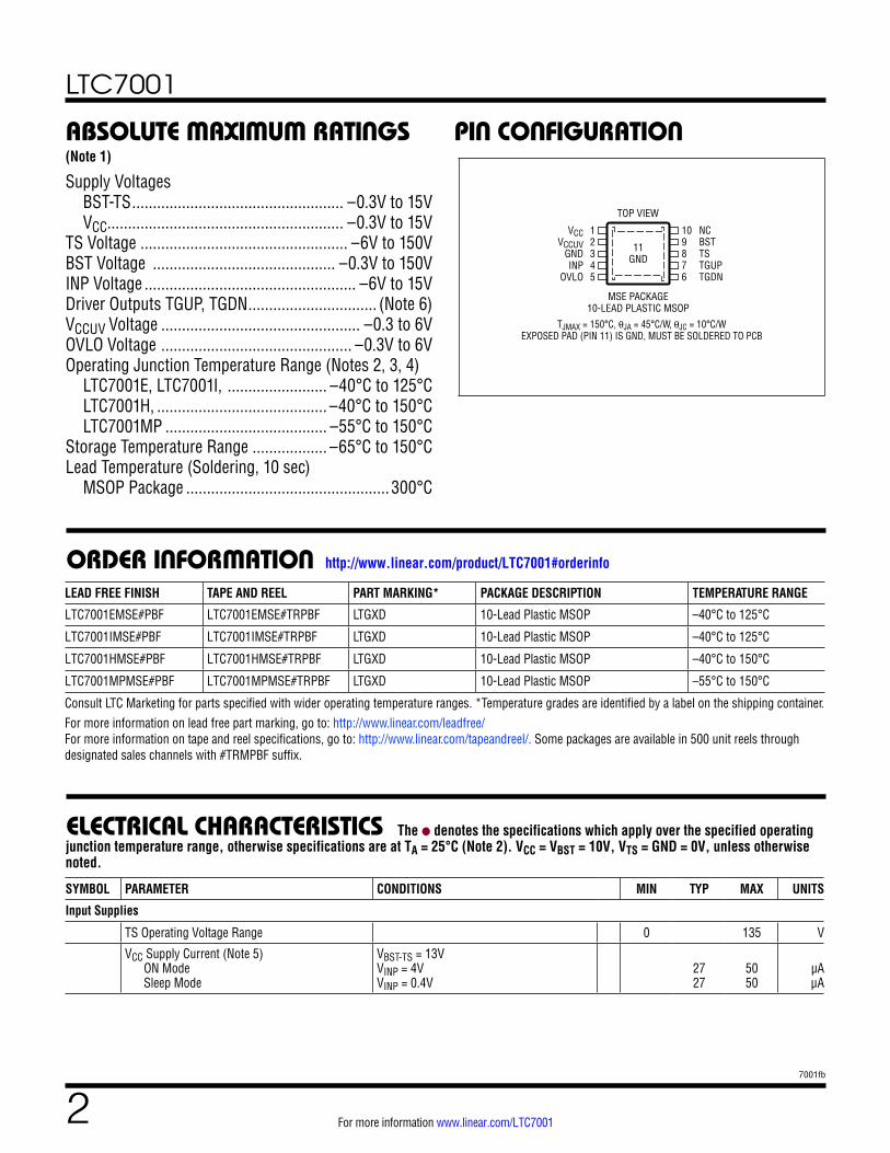
pin conFiguraTionabsoluTe MaxiMuM raTings
Supply Voltages BST-TS ................................................... –0.3V to 15V VCC......................................................... –0.3V to 15VTS Voltage .................................................. –6V to 150VBST Voltage ............................................ –0.3V to 150VINP Voltage ................................................... –6V to 15VDriver Outputs TGUP, TGDN ............................... (Note 6)VCCUV Voltage ................................................ –0.3 to 6VOVLO Voltage .............................................. –0.3V to 6VOperating Junction Temperature Range (Notes 2, 3, 4) LTC7001E, LTC7001I, ........................ –40°C to 125°C LTC7001H, ......................................... –40°C to 150°C LTC7001MP ....................................... –55°C to 150°CStorage Temperature Range .................. –65°C to 150°CLead Temperature (Soldering, 10 sec) MSOP Package ................................................. 300°C
(Note 1)
orDer inForMaTionLEAD FREE FINISH TAPE AND REEL PART MARKING* PACKAGE DESCRIPTION TEMPERATURE RANGE
LTC7001EMSE#PBF LTC7001EMSE#TRPBF LTGXD 10-Lead Plastic MSOP –40°C to 125°C
LTC7001IMSE#PBF LTC7001IMSE#TRPBF LTGXD 10-Lead Plastic MSOP –40°C to 125°C
LTC7001HMSE#PBF LTC7001HMSE#TRPBF LTGXD 10-Lead Plastic MSOP –40°C to 150°C
LTC7001MPMSE#PBF LTC7001MPMSE#TRPBF LTGXD 10-Lead Plastic MSOP –55°C to 150°C
Consult LTC Marketing for parts specified with wider operating temperature ranges. *Temperature grades are identified by a label on the shipping container.For more information on lead free part marking, go to: http://www.linear.com/leadfree/ For more information on tape and reel specifications, go to: http://www.linear.com/tapeandreel/. Some packages are available in 500 unit reels through designated sales channels with #TRMPBF suffix.
12345
VCCVCCUV
GNDINP
OVLO
109876
NCBSTTSTGUPTGDN
TOP VIEW
MSE PACKAGE10-LEAD PLASTIC MSOP
11GND
TJMAX = 150°C, θJA = 45°C/W, θJC = 10°C/W
EXPOSED PAD (PIN 11) IS GND, MUST BE SOLDERED TO PCB
SYMBOL PARAMETER CONDITIONS MIN TYP MAX UNITS
Input Supplies
TS Operating Voltage Range 0 135 V
VCC Supply Current (Note 5) ON Mode Sleep Mode
VBST-TS = 13V VINP = 4V VINP = 0.4V
27 27
50 50
µA μA
http://www.linear.com/product/LTC7001#orderinfo
The l denotes the specifications which apply over the specified operating junction temperature range, otherwise specifications are at TA = 25°C (Note 2). VCC = VBST = 10V, VTS = GND = 0V, unless otherwise noted.
elecTrical characTerisTics

LTC7001
37001fb
For more information www.linear.com/LTC7001
elecTrical characTerisTics The l denotes the specifications which apply over the specified operating junction temperature range, otherwise specifications are at TA = 25°C (Note 2). VCC = VBST = 10V, VTS = GND = 0V, unless otherwise noted.SYMBOL PARAMETER CONDITIONS MIN TYP MAX UNITS
VCC UVLO VCC Undervoltage Lockout VCCUV = OPEN VCC Rising VCC Falling Hysteresis VCCUV = 0V VCC Rising VCC Falling Hysteresis VCCUV = 1.5V VCC Rising VCC Falling Hysteresis
l
l
l
l
6.5 5.8
3.1 2.8
9.7 9.1
7.0 6.4 600
3.5 3.2 300
10.5 9.9 600
7.5 6.9
3.7 3.4
10.9 10.3
V V
mV
V V
mV
V V
mV
Bootstrapped Supply (BST-TS)
VBST-TS VTG Above VTS with INP = 3V (DC) VCC = VTS = 7V, IBST = 0µA VCC = VTS = 10V, IBST = 0µA VTS = 135V, IBST = 0µA
l
l
9 10 10
11 12 12
14 14 14
V V V
Charge Pump Output Current VTS = 20V, VBST-TS = 10V l –15 –30 µA
BST-TS Floating UVLO VBST-TS Rising VBST-TS Falling
3.1 2.8
V V
Output Gate Driver (TG)
TG Pull-Up Resistance VCC = VBST = 12V l 2.2 7 Ω
TG Pull-Down Resistance VCC = VBST = 12V l 1 4 Ω
tr Output Rise Time 10% to 90%, CL = 1nF 10% to 90%, CL = 10nF
13 90
ns ns
tf Output Fall Time 10% to 90%, CL = 1nF 10% to 90%, CL = 10nF
13 40
ns ns
tPLH tPHL
Input to Output Propagation Delay VINP Rising, CL = 1nF VINP Falling, CL = 1nF
l
l
35 35
70 70
ns ns
Operation
VIH VIL
Input Threshold Voltages VINP Rising VINP Falling Hysteresis
l
l
1.7 1.3
2 1.6 400
2.2 1.8
V V
mV
Input Pull-Down Resistance VINP = 1V 1 MΩ
OVLO Pin Threshold Voltage Rising Falling Hysteresis
1.16 1.05
1.21 1.10 110
1.26 1.15
V V
mV
OVLO Pin Leakage Current VOVLO = 1.3V –100 0 100 nA
VVCCUV Pull-Up Current VVCCUV = 1V –11.3 –10 8.7 µA
Note 1: Stresses beyond those listed under Absolute Maximum Ratings may cause permanent damage to the device. Exposure to any Absolute Maximum Rating condition for extended periods may affect device reliability and lifetime.Note 2: The LTC7001 is tested under pulsed load conditions such that TJ ≈ TA. The LTC7001E is guaranteed to meet performance specifications from 0°C to 85°C. Specifications over the –40°C to 125°C operating junction temperature range are assured by design, characterization and correlation with statistical process controls. The LTC7001I is guaranteed over the –40°C to 125°C operating junction temperature range, the
LTC7001H is guaranteed over the –40°C to 150°C operating junction temperature range and the LTC7001MP is tested and guaranteed over the –55°C to 150°C operating junction temperature range. High junction temperatures degrade operating lifetimes; operating lifetime is derated for junction temperatures greater than 125°C. Note that the maximum ambient temperature consistent with these specifications is determined by specific operating conditions in conjunction with board layout, the rated package thermal impedance and other environmental factors.

LTC7001
47001fb
For more information www.linear.com/LTC7001
elecTrical characTerisTics
Typical perForMance characTerisTics
VCC Supply Current vs VCC Supply Voltage
Driver On Resistance vs VBST-TS Voltage
Input Threshold Voltage vs VCC Supply Voltage
Charge Pump No-Load Output Voltage vs VTS Charge Pump Load Regulation
Charge Pump Output Current vs VTS
TA = 25°C, unless otherwise noted.
VBST-TS = 13VVCCUV = 0V
VCC VOLTAGE (V)3 6 9 12 15
0
10
20
30
40
50
V CC
SUPP
LY C
URRE
NT (µ
A)
7001 G01
VCCUV = 0V TGUPTGDN
VBST-TS (V)3 6 9 12 15
0
1
2
3
4
5
6
R DSO
N (Ω
)
7001 G02
VIN = VCC RISINGFALLING
VCC VOLTAGE (V)3 6 9 12 15
0
0.5
1.0
1.5
2.0
2.5
3.0
THRE
SHOL
D VO
LTAG
E (V
)
7001 G03
IBST = 0µA
VCC = 4VVCC = 5VVCC = 6VVCC = 7VVCC ≥ 8V
VTS (V)0 5 10 15 20
0
2
4
6
8
10
12
14
V BST
- V
TS (V
)
7001 G04
VCC = 7VVBST-TS = 10V
25°C150°C
VTS (V)0 28 56 84 112 140
–45
–35
–25
–15
–5
5
I BST
(µA)
7001 G6
VCC = 4V VTS = 4VVTS = 6VVTS = 8VVTS = 10VVTS = 12V
IBST (µA)0 –20 –40 –60 –80
–1
1
3
5
7
9
11
13
15
V BST
-VTS
(V)
7001 G05
Note 3: The junction temperature (TJ, in °C) is calculated from the ambient temperature (TA, in °C) and power dissipation (PD, in Watts) according to the formula:
TJ = TA + (PD • θJA), where θJA is 45°C/W.Note 4: This IC includes over temperature protection that is intended to protect the device during momentary overload conditions. The maximum rated junction temperature will be exceeded when this protection is active. Operation above the specified absolute maximum operating junction temperature may impair device reliability or permanently damage the device.
Note 5: Dynamic supply current is higher due to the gate charge being delivered at the switching frequency. See Applications Information.Note 6: Do not apply a voltage or current source to these pins. They must be connected to capacitive loads only; otherwise permanent damage may occur.

LTC7001
57001fb
For more information www.linear.com/LTC7001
Typical perForMance characTerisTics
OVLO Threshold Voltage vs Temperature VCCUV Lockout vs Temperature
Driver On Resistance vs Temperature
VCC Supply Current vs Temperature
Input Threshold Voltage vs Temperature
VBST-TS Floating UVLO Voltage vs Temperature
TA = 25°C, unless otherwise noted.
RISINGFALLING
TEMPERATURE (°C)–50 0 50 100 150
1.05
1.10
1.15
1.20
1.25
THRE
SHOL
D VO
LTAG
E (V
)
7001 G07
VCCUV = OPEN RISINGFALLING
TEMPERATURE (°C)–50 0 50 100 150
5.0
5.5
6.0
6.5
7.0
7.5
8.0
V CCU
V LO
CKOU
T (V
)
7001 G08
VBST–TS = 12V TGUPTGDN
TEMPERATURE (°C)–50 0 50 100 150
0
1
2
3
4
RESI
STAN
CE (Ω
)
7001 G09
VIN = 10V
TEMPERATURE (°C)–50 0 50 100 150
15
20
25
30
35
40
CURR
ENT
(µA)
7001 G10
VIN = 10V RISINGFALLING
TEMPERATURE (°C)–50 0 50 100 150
0
0.5
1.0
1.5
2.0
2.5
3.0
THRE
SHOL
D VO
LTAG
E (V
)
7001 G11
RISINGFALLING
TEMPERATURE (°C)–50 0 50 100 150
2.0
2.5
3.0
3.5
4.0
THRE
SHOL
D VO
LTAG
E (V
)
7001 G12
pin FuncTionsVCC (Pin 1): Main Supply Pin. A bypass capacitor with a minimum value of 0.1µF should be tied between this pin and GND.
VCCUV (Pin 2): VCC Supply Undervoltage Lockout. A resistor on this pin sets the reference for the Gate Drive undervoltage lockout. The voltage on this pin in the range of 0.5V to 1.5V is multiplied by seven to be the undervolt-age lockout for the Gate Drive (VCC pin). Short to ground to set the minimum gate drive UVLO of 3.5V. Leave open to set gate drive UVLO to 7.0V
GND (Pin 3, Exposed Pad Pin 11): Ground. The exposed pad must be soldered to the PCB for rated electrical and thermal performance.
INP (Pin 4): Input Signal. CMOS compatible input refer-ence to GND that sets the state of TGDN and TGUP pins (see Applications Information). INP has an internal 1MΩ pull-down to GND to keep TGDN pulled to TS during startup transients.

LTC7001
67001fb
For more information www.linear.com/LTC7001
block DiagraM
7001 BD
2
5
4
3
–
+
–
+
CHARGEPUMP
LEVELSHIFT
UP
LOGIC
TGDN
TS
NC
TGUP
BST
M1
CB0.1µ
D1*
LOAD
1.21V
10µA
2.3V
OVLO
INP
GND
*OPTIONAL
VCCUV
VIN135V ABS MAX
VCC3.5V TO 15V
VCC
1M
PCH
NCH
9
7
6
8
10
1
OVLO (Pin 5): Overvoltage Lockout Input. Connect to the input supply through a resistor divider to set the lockout level. A voltage on this pin above 1.21V causes TGDN to be pulled to TS. Normal operation resumes when the voltage on this pin decreases below 1.11V. OVLO should be tied to GND when not used.
TGDN (Pin 6): High Current Gate Driver Pull-Down. This pin pulls down to TS. For the fastest turn-off, tie this pin directly to the gate of the external high side MOSFET.
TGUP (Pin 7): High Current Gate Driver Pull-Up. This pin pulls up to BST. Tie this pin to TGDN for maximum gate drive transition speed. A resistor can be connected
between this pin and the gate of the external MOSFET to control the inrush current during turn-on. See Applications Information.
TS (Pin 8): Top (High Side) source connection or GND if used in ground referenced applications.
BST (Pin 9): High Side Bootstrapped Supply. An external capacitor with a minimum value of 0.1µF should be tied between this pin and TS. Voltage swing on this pin is 12V to (VTS + 12V).
NC (Pin 10): No Connect. This pin should be floated.
pin FuncTions

LTC7001
77001fb
For more information www.linear.com/LTC7001
operaTionThe LTC7001 is designed to receive a ground-referenced, low voltage digital input signal, INP and quickly drive a high side N-channel power MOSFET whose drain can be up to 150V above ground. The LTC7001 is capable of driv-ing a 1nF load using a 12V bootstrapped supply voltage (VBST–VTS) with 35ns of propagation delay and fast rise/fall times. The high gate drive voltage reduces external power losses associated with external MOSFET on-resistance. The strong drivers not only provide fast turn on and off times but hold the TGUP and TGDN to TS voltages in the desired state in the presence of high slew rate transients which can occur driving inductive loads at high voltages.
Internal Charge Pump
The LTC7001 contains an internal charge pump that enables the MOSFET gate drive to have 100% duty cycle. The charge pump regulates the BST-TS voltage to 12V reducing external power losses associated with external MOSFET on-resistance. The charge pump uses the higher voltage of TS or VCC as the source for the charge.
Protection Circuitry
When using the LTC7001, care must be taken not to exceed any of the ratings specified in the Absolute Maximum Ratings section. As an added safeguard, the LTC7001
incorporates an overtemperature shutdown feature. If the junction temperature reaches approximately 180°C, the LTC7001 will enter thermal shutdown mode and TGDN will be pulled to TS. After the part has cooled below 160°C, TGDN will be allowed to go back high. The overtemperature level is not production tested. The LTC7001 is guaranteed to start at temperatures below 150°C.
The LTC7001 additionally implements protection fea-tures which prohibit TGDN from going high when VCC or (VBST–VTS) are not within proper operating ranges. By using a resistive divider from VIN to ground the OVLO pin can serve as a precise input supply voltage overvoltage lockout. TGDN is pulled to TS when OVLO rises above 1.21V, so OVLO can be configured to limit switching to a specific range on input supply voltages.
VCC contains an undervoltage lockout feature that will pull TGDN to TS and is configured by the VCCUV pin. If VCCUV is open, TGDN is pulled to TS until VCC is greater than 7.0V. By using a resistor from VCCUV to ground, the rising undervoltage lockout on VCC can be adjusted from 3.5V to 10.5V.
An additional internal undervoltage lockout is included that will pull TGDN to TS when the floating voltage from BST to TS is less than 3.1V (typical).
(Refer to Block Diagram)
TiMing DiagraM
INPUT (INP)
OUTPUT (TG-TS)
INPUT RISE/FALL TIME < 10ns
tPLH
trtPHL
tf
90%10%
VIHVIL
7001 TD

LTC7001
87001fb
For more information www.linear.com/LTC7001
applicaTions inForMaTionInput Stage
The LTC7001 employs CMOS compatible input thresholds that allow a low voltage digital signal connected to INP to drive standard power MOSFETs. The LTC7001 contains an internal voltage regulator which biases the input buffer connected to INP allowing the input thresholds (VIH = 2.0V, VIL = 1.6V) to be independent of variations in VCC. The 400mV hysteresis between VIH and VIL eliminates false triggering due to noise events. However, care should be taken to keep INP from any noise pickup, especially in high frequency, high voltage applications.
INP also contains an internal 1MΩ pull-down resistor to ground, keeping TGDN pulled to TS during startup and other unknown transient events.
INP has an Absolute Maximum of –6V to +15V which allows the signal driving INP to have voltage excursions outside the normal power supply and ground range. It is not uncommon for signals routed with long PCB traces and driven with fast rise/fall times to inductively ring to voltages higher than power supply or lower than ground.
Output Stage
A simplified version of the LTC7001 output stage is shown in Figure 1. The pull-down device is an N-channel MOSFET with a typical 1Ω RDS(ON) and the pull-up device is a P-channel MOSFET with a typical 2.2Ω RDS(ON). The pull-up and pull-down pins have been separated to allow the turn-on transient to be controlled while maintaining a fast turn-off.
The LTC7001 powerful output stage (1Ω pull-down and 2.2Ω pull-up) minimizes transition losses when driving external MOSFETs and keeps the MOSFET in the state com-manded by INP even if high voltage and high frequency transients couple from the power MOSFET back to the driving circuitry.
The large gate drive voltage on TGUP and TGDN reduces conduction losses in the external MOSFET because RDS(ON) is inversely proportional to its gate overdrive (VGS – VTH).
External Overvoltage Lockout
The OVLO pin can be configured as a precise overvoltage (OVLO) lockout on the VIN supply with a resistive divider from VIN to ground. A simple resistive divider can be used as shown in Figure 2 to meet specific VIN voltage require-ments. When OVLO is greater than 1.21V, TGDN will be pulled to TS and the external MOSFET will be turned off.
Figure 1. Simplified Output Stage
Figure 2. Adjustable OV Lockout
BST
TGUP
TGDN
TS
VCC
INP
12V
7001 F01
+–
+–
2.2Ω
1Ω
HIGH SPEED150V LEVEL
SHIFTER
CHARGEPUMP 30µA
LTC7001
AV = 1
The current that flows through the R4 – R5 divider will directly add to the current drawn from VIN and care should be taken to minimize the impact of this current on the overall current used by the application circuit. Resistor values in the megaohm range may be required to keep the impact of the quiescent shutdown and sleep currents low. To pick resistor values, the sum total of R4 + R5 (RTOTAL) should
VIN
R4
R5D5 7001 F02
LTC7001
OVLO

LTC7001
97001fb
For more information www.linear.com/LTC7001
applicaTions inForMaTionbe chosen first based on the allowable DC current that can be drawn from VIN. The individual values of R4 and R5 can then be calculated from the following equations:
R5 = RTOTAL •
1.21VRising VIN OVLO Threshold
R4 = RTOTAL – R5
For applications that do not need a precise external OVLO the OVLO pin is required to be tied directly to ground.
Be aware that the OVLO pin cannot be allowed to exceed its absolute maximum rating of 6V. To keep the voltage on the OVLO pin from exceeding 6V, the following relationship should be satisfied:
VIN(MAX) •
R5R4 + R5
< 6V
If the VIN(MAX) relationship for the OVLO pin cannot be satisfied, an external 5V Zener diode should also be placed from OVLO to ground in addition to any lockout setting resistors.
Bootstrapped Supply (BST-TS)
An external bootstrapped capacitor, CB, connected between BST and TS supplies the gate drive voltage for the MOSFET driver. The LTC7001 keeps the BST-TS supply charged with an internal charge pump, allowing for duty cycles up to 100 %. When the high side external MOSFET is to be turned on, the driver places the CB voltage across the gate-source of the MOSFET. This enhances the high side MOSFET and turns it on. The source of the MOSFET, TS, rises to VIN and the BST pin follows. With the high side MOSFET on, the BST voltage is above the input supply; VBST = VTS + 12V. The boost capacitor, CB, supplies the charge to turn on the external MOSFET and needs to have at least 10 times the charge to turn on the external MOSFET fully. The charge to turn on the external MOSFET is referred to gate charge, QG, and is typically specified in the external MOSFET data sheet. Gate charge can range from 5nC to hundreds nCs and is influenced by the gate
drive level and the type of external MOSFET used. For most applications, a capacitor value of 0.1µF for CB will be sufficient. However, the following relationship for CB should be maintained:
CB > 10 •External MOSFET QG
1VThe internal charge pump that charges the BST-TS supply outputs approximately 30µA to the BST pin. If the time to charge the external bootstrapped capacitor, CB from initial power-up with the internal charge pump is not sufficient for the application, a low reverse leakage external silicon diode, D1 with a reverse voltage rating greater than VIN connected between VCC and BST should be used as shown in Figure 3. An external silicon diode between VCC and BST should be used if the following relationship cannot be met:
BST Diode Required if Power-Up to INP Going High
<CBST •12V
30µA≅ 40ms
Figure 3. External BST Diode
CB
D1VCC
BST
TS7001 F03
LTC7001
Another reason to use an external silicon diode between VCC and BST is if the external MOSFET is switched at frequency so high that the BST-TS supply collapses. An external silicon diode between VCC and BST should be used if the following relationship cannot be met:
BST Diode Required if Switching Frequency
> 30µA2 •MOSFET QG
≅ 500Hz

LTC7001
107001fb
For more information www.linear.com/LTC7001
applicaTions inForMaTionA Schottky diode should not be used between VCC and BST, because the reverse leakage of the Schottky diode at hot will be more current than the charge pump can overcome.
Some example silicon diodes with low leakage include:
• MMBD1501A, Fairchild Semiconductor
• CMPD3003, Central Semiconductor
VCC Undervoltage Comparator
The LTC7001 contains an adjustable undervoltage lockout (UVLO) on the VCC voltage that pulls TGDN to TS and can be easily programmed using a resistor (RVCCUV) between the VCCUV pin and ground. The voltage generated on VCCUV by RVCCUV and the internal 10µA current source set the VCC UVLO. The rising VCC UVLO is internally limited within the range of 3.5V and 10.5V. If VCCUV is open the rising VCC UVLO is set internally to 7.0V. The typical value of resistor for a particular rising VCC UVLO can be selected using Figure 4 or the following equation:
RVCCUV = Rising VCC UVLO
70µA
Where 3.5V < Rising VCC UVLO < 10.5V.
MOSFET Selection
The most important parameters in high voltage applications for MOSFET selection are the breakdown voltage BVDSS, on-resistance RDS(ON) and the safe operating area, SOA.
The MOSFET, when off, will see the full input range of the input power supply plus any additional ringing than can occur when driving an inductive load.
External conduction losses are minimized when using low RDS(ON) MOSFETs. Since many high voltage MOSFETs have higher threshold voltages (typical VTH ≥ 5V) and RDS(ON) is directly related to the (VGS–VTH) of the MOSFET, the LTC7001 maximum gate drive of greater than 10V makes it an ideal solution to minimize external conduction losses associated with external high voltage MOSFETs.
SOA is specified in Typical Characteristic curves in power N-channel MOSFET data sheets. The SOA curves show the relationship between the voltages and current allowed in a timed operation of a power MOSFET without causing damage to the MOSFET.
Limiting Inrush Current During Turn-On
Large capacitive loads such as complex electrical systems with large bypass capacitors should be driven using the circuit shown in Figure 5. The pull-up gate drive to the power MOSFET from TGUP is passed through an RC delay network, RG and CG, which greatly reduces the turn-on ramp rate of the MOSFET. Since the MOSFET source volt-age follows the gate voltage, the load is powered smoothly from ground. This dramatically reduces the inrush current from the source supply and reduces the transient ramp rate of the load, allowing for slower activation of sensitive electrical loads. The turn-off of the MOSFET is not affected by the RC delay network as the pull-down for the MOSFET gate is directly from the TGDN pin. Note that the voltage rating on capacitor CG needs to be the same or higher than the external MOSFET and CLOAD.
Figure 4. VCCUV Resistor Selection
RISING VCC UVLOFALLING VCC UVLO
VCCUV RESISTOR TO GROUND (kΩ)0 30 60 90 120 150 180 210 240
0
1
2
3
4
5
6
7
8
9
10
11
V CC
UVLO
(V)
7000 F04

LTC7001
117001fb
For more information www.linear.com/LTC7001
applicaTions inForMaTionAdding CG to the gate of the external MOSFET can cause high frequency oscillation. A low power, low ohmic value resistor (10Ω) should be placed in series with CG to dampen the oscillations as shown in Figure 5 whenever CG is used in an application. Alternatively, the low ohmic value resistor can be placed in series with the gate of the external MOSFET.
Figure 6. Optional Schottky Diode Usage
When CG is added to the circuit in Figure 5, the value of the bootstrap capacitor, CB, must be increased to be able to supply the charge to both to MOSFET gate and capacitor CG. The relationship for CB that needs to be maintained when CG is used is given by:
CB > 10 •MOSFET QG
1V+ 10 •CG
Optional Schottky Diode Usage on TS
When turning off a power MOSFET that is connected to an inductive component (inductor, long wire or complex load), the TS pin can be pulled below ground until the current in the inductive component has completely discharged. The TS pin is tolerant of voltages down to –6V, however, an optional Schottky diode with a voltage rating at least as high as the load voltage should be connected between TS and ground to prevent discharging the inductive through the TS pin of the LTC7001. See Figure 6.Figure 5. Powering Large Capacitive Loads
The values for RG and CG to limit the inrush current can be calculated from the below equation:
IIN _RUSH ≅
0.7 •12V •CLOADRG •CG
For the values shown in Figure 5 the inrush current will be:
IIN _RUSH ≅ 0.7 •12V •100µF
100kΩ • 0.047µF≅ 180mA
Correspondingly, the ramp rate at the load for the circuit in Figure 5 is approximately:
Δ VLOADΔT
≅ 0.7 •12VRG •CG
≅ 2V/ ms
L1
TGUP
TGDN
TS
7001 F06
LTC7001
M1A
VIN
LOAD
D2
CB1µF
CG47nF
10Ω
LOAD
BST
TS
TGUPTGDN
RG100k
7001 F05
LTC7001
VIN
CLOAD100µF

LTC7001
127001fb
For more information www.linear.com/LTC7001
Figure 7. Protecting Load from Voltage Drops on VIN
TGUP
TGDN
TSINP
7001 F07
LTC7001
M1A
M1B
VIN
LOAD
Reverse Input Protection
To protect the load from discharging back into VIN when the external MOSFET is off and the VIN voltage drops below the load voltage, two external N-channel MOSFETs should be used and must be in a back-to-back arrangement as shown in Figure 7. Dual N-channel packages such as the Vishay/Siliconix Si7956DP are a good choice for space saving designs.
PC Board Layout Considerations
1. Solder the exposed pad on the backside of the LTC7001 package directly to the ground plane of the board.
2. Limit the resistance of the TS trace, by making it short and wide.
3. CB needs to be close to chip.
4. Always include an option in the PC board layout to place a resistor in series with the gate of any external MOSFET. High frequency oscillations are design dependent, and having the option to add a series dampening resistor can save a design iteration of the PC board.
applicaTions inForMaTion

LTC7001
137001fb
For more information www.linear.com/LTC7001
Typical applicaTions
High Side Switch with Inrush Control and OVLO
High Side Switch with VCCUV and OVLO
4.7µF
0.47µF
220k
LOAD15mF0V TO 60V
47µF+1µF
TGUPTGDN
BST
TS
OVLO
INP
VCC
VCCUV
7001 TA02
LTC7001
IRFS4115PBF
DFLS1150
VIN0V TO 60V
(150V TOLERANT)
VCC7V TO 15V
ONOFF
GND
590k
10Ω
12.1k
0.1µFLOAD0V TO 100V
TGUPTGDN
BST
TS
OVLO
INP
VCCUV
VCC
7001 TA03
LTC7001
BSC12DN20NS3G
VIN0V TO 100V
(150V TOLERANT)
VCC5V TO 15V
ONOFFGND
12.1k976k
71.5k
LTC7001
147001fb
For more information www.linear.com/LTC7001
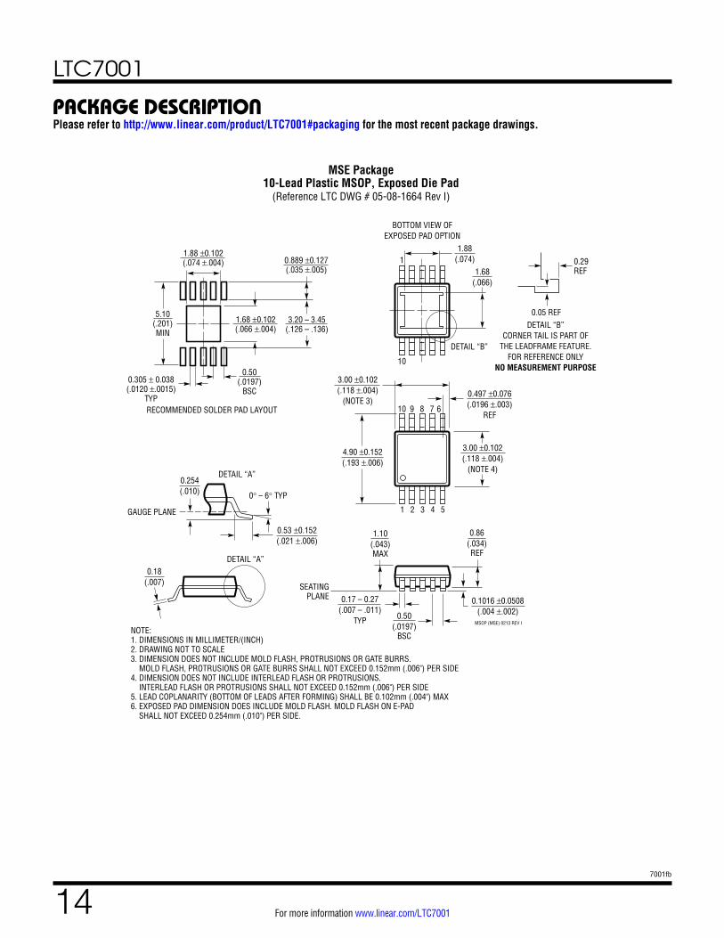
package DescripTionPlease refer to http://www.linear.com/product/LTC7001#packaging for the most recent package drawings.
MSOP (MSE) 0213 REV I
0.53 ±0.152(.021 ±.006)
SEATINGPLANE
0.18(.007)
1.10(.043)MAX
0.17 – 0.27(.007 – .011)
TYP
0.86(.034)REF
0.50(.0197)
BSC
1 2 3 4 5
4.90 ±0.152(.193 ±.006)
0.497 ±0.076(.0196 ±.003)
REF8910
10
1
7 6
3.00 ±0.102(.118 ±.004)
(NOTE 3)
3.00 ±0.102(.118 ±.004)
(NOTE 4)
NOTE:1. DIMENSIONS IN MILLIMETER/(INCH)2. DRAWING NOT TO SCALE3. DIMENSION DOES NOT INCLUDE MOLD FLASH, PROTRUSIONS OR GATE BURRS. MOLD FLASH, PROTRUSIONS OR GATE BURRS SHALL NOT EXCEED 0.152mm (.006") PER SIDE4. DIMENSION DOES NOT INCLUDE INTERLEAD FLASH OR PROTRUSIONS. INTERLEAD FLASH OR PROTRUSIONS SHALL NOT EXCEED 0.152mm (.006") PER SIDE5. LEAD COPLANARITY (BOTTOM OF LEADS AFTER FORMING) SHALL BE 0.102mm (.004") MAX6. EXPOSED PAD DIMENSION DOES INCLUDE MOLD FLASH. MOLD FLASH ON E-PAD SHALL NOT EXCEED 0.254mm (.010") PER SIDE.
0.254(.010) 0° – 6° TYP
DETAIL “A”
DETAIL “A”
GAUGE PLANE
5.10(.201)MIN
3.20 – 3.45(.126 – .136)
0.889 ±0.127(.035 ±.005)
RECOMMENDED SOLDER PAD LAYOUT
1.68 ±0.102(.066 ±.004)
1.88 ±0.102(.074 ±.004)
0.50(.0197)
BSC0.305 ± 0.038(.0120 ±.0015)
TYP
BOTTOM VIEW OFEXPOSED PAD OPTION
1.68(.066)
1.88(.074)
0.1016 ±0.0508(.004 ±.002)
DETAIL “B”
DETAIL “B”CORNER TAIL IS PART OF
THE LEADFRAME FEATURE.FOR REFERENCE ONLY
NO MEASUREMENT PURPOSE
0.05 REF
0.29REF
MSE Package10-Lead Plastic MSOP, Exposed Die Pad
(Reference LTC DWG # 05-08-1664 Rev I)

LTC7001
157001fb
For more information www.linear.com/LTC7001
Information furnished by Linear Technology Corporation is believed to be accurate and reliable. However, no responsibility is assumed for its use. Linear Technology Corporation makes no representa-tion that the interconnection of its circuits as described herein will not infringe on existing patent rights.
revision hisToryREV DATE DESCRIPTION PAGE NUMBER
A 07/17 Clarified second paragraph in the Output Surge sectionChanged to Zener from Schottky diode (text and symbol)Modified equation, updated Figure 4INP = 0 in Figure 7, and wording updateSchematic clarification
99, 10
111314
B 10/17 Top mark corrected 2

LTC7001
167001fb
For more information www.linear.com/LTC7001
LT 1017 REV B • PRINTED IN USAwww.linear.com/LTC7001
LINEAR TECHNOLOGY CORPORATION 2017
relaTeD parTs
Typical applicaTion
PART NUMBER DESCRIPTION COMMENTS
LTC7000/LTC7000-1 Fast 150V Protected High Side NMOS Static Switch Driver
3.5V to 150V Operation, Short-Circuit Protected, ΔVSNS = 30mV, IQ = 35µA, Turn-On (CL = 1nF) = 35ns, Internal Charge Pump
LTC4440/LTC4440-5/LTC4440A-5
High Speed, High Voltage High Side Gate Driver Up to 100V Supply Voltage, 8V ≤ VCC ≤ 15V, 2.4A Peak Pull-Up/1.5Ω Peak Pull-Down
LTC7138 High Efficiency, 150V 250mA/400mA Synchronous Step-Down Regulator
Integrated Power MOSFETs, 4V ≤ VIN ≤ 150V, 0.8V ≤ VOUT ≤ VIN, IQ = 12µA, MSOP-16 (12)
LTC7103 105V, 2.3A Low EMI Synchronous Step-Down Regulator
4.4V ≤ VIN ≤ 105V, 1V ≤ VOUT ≤ VIN, IQ = 2µA Fixed Frequency 200kHz to 2MHz, 5mm × 6mm QFN
LTC7801 150V Low IQ, Synchronous Step-Down DC/DC Controller 4V ≤ VIN ≤ 140V, 150V Abs Max, 0.8V ≤ VOUT ≤ 60V, IQ = 40µA, PLL Fixed Frequency 320kHz to 2.25MHz
LT1910 Protected High Side MOSFET Driver 8V to 48V Operation, ΔVSNS = 65mV, IQ = 110µA, Turn-On (CL = 1nF) = 220µs, Internal Charge Pump
LTC4367 100V Overvoltage, Undervoltage and Reverse Supply Protection
2.5V ≤ VIN ≤ 60V, VOUT Protection Up to 100V, Reverse Protection to –40V, MSOP-8, 3mm × 3mm DFN-8
LTC4368 100V Overvoltage, Undervoltage and Revernse Protection Controller with Bidirectional Circuit Breaker
2.5V ≤ VIN ≤ 60V, VOUT Protection Up to 100V, Reverse Protection to –40V, MSOP-8, 3mm × 3mm DFN-8
LTC4364 Surge Stopper with Ideal Diode 4V to 80V Operation, ΔVSNS = 50mV, IQ = 425µA, Turn-On (CL = 1nF) = 500µs, Internal Charge Pump
LTC7860 High Efficiency Switching Surge Stopper 4V to 60V Operation, ΔVSNS = 95mV, IQ = 370µA, PMOS Driver
LTC4231 Micropower Hot Swap Controller 2.7V to 36V Operation, ΔVSNS = 50mV, IQ = 4µA, Turn-On (CL = 1nF) = 1ms, Internal Charge Pump
LTC3895 150V Low IQ, Synchronous Step-Down DC/DC Controller PLL Fixed Frequency 50kHz to 900kHz, 4V ≤ VIN ≤ 140V, 0.8V ≤ VOUT ≤ 60V, IQ = 40µA
LTC4380 Low Quiescent Current Surge Stopper 4V to 80V Operation, ΔVSNS = 50mV, IQ = 8µA, Turn-On = 5ms, Internal Charge Pump
LTC3639 High Efficiency, 150V 100mA Synchronous Step-Down Regulator
Integrated Power MOSFETs, 4V ≤ VIN ≤ 150V, 0.8V ≤ VOUT ≤ VIN, IQ = 12µA, MSOP-16(12)
Motor Driver
86.6k
VS-12CWQ10FN
TGUPTGDN
TS
VCCUV
VCC
BST
OVLO
INP
7001 TA04
LTC7001
BSC252N10NS
VCC6V TO 15V
PWM - 20kHz
CMPD3003 0.1µF48V
GND48V, 500W MOTORM