LTC4366 - High Voltage Surge Stopper - analog.com · LTC4366 436612fe 6 For more information VSS...
24
LTC4366 436612fe For more information www.linear.com/LTC4366 1 TYPICAL APPLICATION FEATURES DESCRIPTION High Voltage Surge Stopper The LTC ® 4366 surge stopper protects loads from high voltage transients. By controlling the gate of an external N-channel MOSFET, the LTC4366 regulates the output during an overvoltage transient. The load may remain operational while the overvoltage is dropped across the MOSFET. Placing a resistor in the return line isolates the LTC4366 and allows it to float up with the supply; therefore, the upper limit on the output voltage depends only on the availability of high valued resistors and MOSFET ratings. An adjustable overvoltage timer prevents MOSFET dam- age during the surge while an additional 9-second timer provides for MOSFET cool down. A shutdown pin reduces the quiescent current to less than 14µA during shutdown. After a fault the LTC4366-1 latches off while the LTC4366-2 will auto-retry. Overvoltage Protected 1.5A, 28V Supply Overvoltage Protector Regulates Output at 43V During Transient APPLICATIONS n Rugged Floating Topology n Wide Operating Voltage Range: 9V to >500V n Adjustable Output Clamp Voltage n Controls N-Channel MOSFET n Adjustable Protection Timer n Internal 9-Second Cool-Down Timer n Shutdown I Q < 14µA n 8-Lead TSOT and 3mm × 2mm DFN Packages n Industrial, Automotive and Avionic Surge Protection n High Voltage DC Distribution n 28V Vehicle Systems L, LT, LTC, LTM, Linear Technology and the Linear logo are registered trademarks and ThinSOT is a trademark of Linear Technology Corporation. All other trademarks are the property of their respective owners. Patents pending. V DD OUT 2nF GATE IXTK90N25L2 SD FB 1μF 0.47μF 12.4k V OUT 1.5A V IN 28V 422k 436612 TA01a 46.4k 10Ω 324k LTC4366-2 TIMER BASE V SS 28V 100ms/DIV 436612 TA01b 28V 43V CLAMP 250V INPUT SURGE V IN 100V/DIV V OUT 20V/DIV
Transcript of LTC4366 - High Voltage Surge Stopper - analog.com · LTC4366 436612fe 6 For more information VSS...

LTC4366
436612fe
For more information www.linear.com/LTC4366 1
TYPICAL APPLICATION
FEATURES DESCRIPTION
High Voltage Surge Stopper
The LTC®4366 surge stopper protects loads from high voltage transients. By controlling the gate of an external N-channel MOSFET, the LTC4366 regulates the output during an overvoltage transient. The load may remain operational while the overvoltage is dropped across the MOSFET. Placing a resistor in the return line isolates the LTC4366 and allows it to float up with the supply; therefore, the upper limit on the output voltage depends only on the availability of high valued resistors and MOSFET ratings.
An adjustable overvoltage timer prevents MOSFET dam-age during the surge while an additional 9-second timer provides for MOSFET cool down. A shutdown pin reduces the quiescent current to less than 14µA during shutdown. After a fault the LTC4366-1 latches off while the LTC4366-2 will auto-retry.
Overvoltage Protected 1.5A, 28V Supply Overvoltage Protector Regulates Output at 43V During Transient
APPLICATIONS
n Rugged Floating Topology n Wide Operating Voltage Range: 9V to >500V n Adjustable Output Clamp Voltage n Controls N-Channel MOSFET n Adjustable Protection Timer n Internal 9-Second Cool-Down Timer n Shutdown IQ < 14µA n 8-Lead TSOT and 3mm × 2mm DFN Packages
n Industrial, Automotive and Avionic Surge Protection n High Voltage DC Distribution n 28V Vehicle Systems
L, LT, LTC, LTM, Linear Technology and the Linear logo are registered trademarks and ThinSOT is a trademark of Linear Technology Corporation. All other trademarks are the property of their respective owners. Patents pending.
VDD OUT
2nF
GATE
IXTK90N25L2
SD FB
1µF
0.47µF
12.4k
VOUT1.5A
VIN28V
422k
436612 TA01a
46.4k
10Ω
324k
LTC4366-2
TIMER BASEVSS
28V
100ms/DIV 436612 TA01b
28V
43V CLAMP
250V INPUT SURGE
VIN100V/DIV
VOUT20V/DIV

LTC4366
436612fe
For more information www.linear.com/LTC43662
ABSOLUTE MAXIMUM RATINGSSupply Voltage (VDD) ................................ –0.3V to 10VSupply Voltage (OUT) ................................. –0.3V to 5VInput Voltages FB .............................................. –0.3V to OUT + 0.3V TIMER ................................................... –0.3V to 3.5V SD .......................................................... –0.3V to 10VOutput Voltages BASE .........................................................–1.5V to 4V OUT – BASE ......................................... –0.3V to 5.5V GATE (Note 3) ........................................ –0.3V to 15V GATE – OUT (Note 3) ............................. –0.3V to 10V
(Notes 1, 2) All voltages relative to VSS, unless otherwise noted.
VDD 1SD 2
TIMER 3VSS 4
8 GATE7 OUT6 FB5 BASE
TOP VIEW
TS8 PACKAGE8-LEAD PLASTIC TSOT-23
TJMAX = 150°C, θJA = 195°C/W
TOP VIEW
9
DDB PACKAGE8-LEAD (3mm × 2mm) PLASTIC DFN
5
6
7
8
4
3
2
1VSS
TIMER
SD
VDD
BASE
FB
OUT
GATE
TJMAX = 150°C,
θJA = 75°C/W IF VSS IS SOLDERED TO PCB, θJA = 135°C/W IF VSS IS NOT SOLDERED TO PCB EXPOSED PAD (PIN 9), PCB VSS CONNECTION OPTIONAL
PIN CONFIGURATION
Currents IVDD ...................................................................10mA IOUT ...................................................................10mA BASE ................................................. –300µA to 10µA SD .......................................................–10mA to 10µAOperating Ambient Temperature Range (Note 4) LTC4366C ................................................ 0°C to 70°C LTC4366I .............................................–40°C to 85°C LTC4366H .......................................... –40°C to 125°C LTC4366MP ....................................... –55°C to 125°CStorage Temperature Range .................. –65°C to 150°CLead Temperature (Soldering, 10 sec) TSOT-23 Package Only .................................... 300°C

LTC4366
436612fe
For more information www.linear.com/LTC4366 3
ORDER INFORMATIONLead Free FinishTAPE AND REEL (MINI) TAPE AND REEL PART MARKING* PACKAGE DESCRIPTION TEMPERATURE RANGE
LTC4366CTS8-1#TRMPBF LTC4366CTS8-1#TRPBF LTFMC 8-Lead Plastic TSOT-23 0°C to 70°C
LTC4366ITS8-1#TRMPBF LTC4366ITS8-1#TRPBF LTFMC 8-Lead Plastic TSOT-23 –40°C to 85°C
LTC4366HTS8-1#TRMPBF LTC4366HTS8-1#TRPBF LTFMC 8-Lead Plastic TSOT-23 –40°C to 125°C
LTC4366CDDB-1#TRMPBF LTC4366CDDB-1#TRPBF LFMD 8-Lead (3mm × 2mm) Plastic DFN 0°C to 70°C
LTC4366IDDB-1#TRMPBF LTC4366IDDB-1#TRPBF LFMD 8-Lead (3mm × 2mm) Plastic DFN –40°C to 85°C
LTC4366HDDB-1#TRMPBF LTC4366HDDB-1#TRPBF LFMD 8-Lead (3mm × 2mm) Plastic DFN –40°C to 125°C
LTC4366CTS8-2#TRMPBF LTC4366CTS8-2#TRPBF LTFMF 8-Lead Plastic TSOT-23 0°C to 70°C
LTC4366ITS8-2#TRMPBF LTC4366ITS8-2#TRPBF LTFMF 8-Lead Plastic TSOT-23 –40°C to 85°C
LTC4366HTS8-2#TRMPBF LTC4366HTS8-2#TRPBF LTFMF 8-Lead Plastic TSOT-23 –40°C to 125°C
LTC4366CDDB-2#TRMPBF LTC4366CDDB-2#TRPBF LFMG 8-Lead (3mm × 2mm) Plastic DFN 0°C to 70°C
LTC4366IDDB-2#TRMPBF LTC4366IDDB-2#TRPBF LFMG 8-Lead (3mm × 2mm) Plastic DFN –40°C to 85°C
LTC4366HDDB-2#TRMPBF LTC4366HDDB-2#TRPBF LFMG 8-Lead (3mm × 2mm) Plastic DFN –40°C to 125°C
LTC4366MPTS8-1#TRMPBF LTC4366MPTS8-1#TRPBF LTFMC 8-Lead Plastic TSOT-23 –55°C to 125°C
LTC4366MPTS8-2#TRMPBF LTC4366MPTS8-2#TRPBF LTFMF 8-Lead Plastic TSOT-23 –55°C to 125°C
LTC4366MPDDB-1#TRMPBF LTC4366MPDDB-1#TRPBF LFMD 8-Lead (3mm × 2mm) Plastic DFN –55°C to 125°C
LTC4366MPDDB-2#TRMPBF LTC4366MPDDB-2#TRPBF LFMG 8-Lead (3mm × 2mm) Plastic DFN –55°C to 125°C
TRM = 500 pieces. *Temperature grades are identified by a label on the shipping container.Consult LTC Marketing for parts specified with wider operating temperature ranges. Consult LTC Marketing for information on lead based finish parts.For more information on lead free part marking, go to: http://www.linear.com/leadfree/ For more information on tape and reel specifications, go to: http://www.linear.com/tapeandreel/

LTC4366
436612fe
For more information www.linear.com/LTC43664
ELECTRICAL CHARACTERISTICS The l denotes the specifications which apply over the full operating temperature range, otherwise specifications are at TA = 25°C. All voltages relative to VSS, unless otherwise noted.
SYMBOL PARAMETER CONDITIONS MIN TYP MAX UNITS
VDD Regulator
VZ(VDD) VDD Shunt Regulator Voltage I = 1mA l 11.5 12 12.5 V
∆VZ(VDD) VDD Shunt Regulator Load Regulation I = 1mA to 5mA LTC4366C/I/H LTC4366MP
l
l
30 30
90 130
mV mV
VDD VDD Supply Voltage (Note 3) l 4.5 VZ(VDD) V
IVDD(STLO) VDD Pin Current – Start-Up, Gate Low GATE = 0V, VDD = 7V, OUT = 0V l 15 23 µA
IVDD(STHI) VDD Pin Current – Start-Up, Gate High GATE Open, VDD = 7V, OUT = 0V l 9 13 µA
IVDD(SD) VDD Pin Current – Shutdown VDD = 7V, OUT = 0V l 5 8 µA
OUT Regulator
VZ(OUT) OUT Shunt Regulator Voltage I = 1mA, BASE = 0V l 5.0 5.7 6.0 V
∆VZ(OUT) OUT Shunt Regulator Load Regulation I = 1mA to 5mA l 30 70 mV
OUT OUT Supply Voltage (Note 3) l 3.0 VZ(OUT) V
VUVLO1 OUT Undervoltage Lockout 1 Rising LTC4366C/I/H LTC4366MP
l
l
2.42 2.42
2.55 2.55
2.75 2.80
V V
∆VUVH1 OUT Undervoltage Lockout 1 Hysteresis l 0.2 0.28 0.4 V
VUVLO2 OUT Undervoltage Lockout 2 Rising l 4.5 4.75 4.9 V
∆VUVH2 OUT Undervoltage Lockout 2 Hysteresis l 0.3 0.4 0.5 V
IOUT(AMP) OUT Pin Current – Regulation Amplifier On l 37 54 µA
IOUT(CP) OUT Pin Current – Charge Pump On l 150 220 µA
IOUT(SD) OUT Pin Current – Shutdown l 3 6 µA
BASE, VSS
VZ(BASE) BASE Shunt Regulator Voltage (OUT – BASE) I = –10µA, OUT = 4.5V l 5.5 6.2 6.6 V
∆VZ(BASE) BASE Shunt Regulator Load Regulation I = –10µA to –80µA, OUT = 4.5V l 125 200 mV
IBASE BASE Pin Leakage Current OUT = 4.5V, BASE = –0.5V l –0.1 –0.8 –5.5 µA
IVSS(AMP) VSS Pin Current – Regulation Amplifier On l –30 –45 –72 µA
IVSS(CP) VSS Pin Current – Charge Pump On l –108 –160 –230 µA
IVSS(SD) VSS Pin Current – Shutdown l –7 –12 µA
GATE Drive
∆VGATE External N-Channel Gate Drive (GATE – OUT) OUT = 4.9V, I = 0, –1µA l 11.2 12 12.5 V
IGATE(ST) GATE Pin Current – Start-Up GATE = OUT = 0V LTC4366C/I/H LTC4366MP
l
l
–4.5 –3.2
–7.5 –7.5
–11 –11
µA µA
IGATE(CP) GATE Pin Current – Charge Pump On GATE = 5V, OUT = 4.9V l –14 –20 –28 µA
IGATE(FD) GATE Pin Current – Fast Discharge GATE = 10V, OUT = 4.9V l 122 200 300 mA
IGATE(FLT) GATE Pin Current – Fault GATE = 10V, OUT = 4.9V l 0.3 0.7 1.2 mA

LTC4366
436612fe
For more information www.linear.com/LTC4366 5
ELECTRICAL CHARACTERISTICS The l denotes the specifications which apply over the full operating temperature range, otherwise specifications are at TA = 25°C. All voltages relative to VSS, unless otherwise noted.
SYMBOL PARAMETER CONDITIONS MIN TYP MAX UNITS
FB, SD, TIMER
VFB(REG) 3% FB pin Regulation Threshold (OUT – FB) l 1.193 1.23 1.267 V
IFB FB Pin Leakage Current OUT – FB = 1.2V l 0 ±1 µA
VSD(TH) SD Pin Threshold Voltage (VDD – SD) Falling l 1.0 1.5 2.3 V
VSD(HYST) SD Pin Hysteresis LTC4366C/I/H LTC4366MP
l
l
147 129
280 280
530 530
mV mV
ISD SD Pin Input Pull-Up Current VDD – SD = 0.7V LTC4366C/I/H LTC4366MP
l
l
–0.7 –0.5
–1.6 –1.6
–3.5 –3.5
µA µA
VTIMER(H) TIMER Pin Threshold TIMER Rising, VDD = 7V, OUT = VZ(OUT) l 2.6 2.8 3.1 V
ITIMER(UP) TIMER Pin Pull-Up Current TIMER = 1V LTC4366C/I/H LTC4366MP
l
l
–5.1 –4
–9 –9
–13 –13
µA µA
ITIMER(DN) TIMER Pin Pull-Down Current TIMER = 1V LTC4366C/I/H LTC4366MP
l
l
0.9 0.7
1.8 1.8
2.8 2.8
µA µA
ITIMER(RATIO) TIMER Pin Current Ratio ITIMER(DN)/ITIMER(UP) l 15 20 25 %
AC Characteristics
tDLY – SD SD Low to Gate Low Filter Time Step VDD – SD from 0V to 3V l 420 700 1200 µs
tDLY – FAST FB Low to Gate Low Delay Time Step OUT – FB from 0V to 1.3V l 60 150 300 ns
tD(COOL) Cool-Down Timer (Internal) VDD = VZ(VDD) LTC4366C/I/H LTC4366MP
l
l
5.9 5.9
9 9
16 19
Seconds Seconds
Note 1: Stresses beyond those listed under Absolute Maximum Ratings may cause permanent damage to the device. Exposure to any Absolute Maximum Rating condition for extended periods may affect device reliability and lifetime.Note 2: All currents into pins are positive.
Note 3: Limits on the maximum rating is defined as whichever limit occurs first. An internal clamp limits the GATE pin to a maximum of 12V above source. Driving this pin to voltages beyond the clamp may damage the device.Note 4: TJ is calculated from the ambient temperature, TA, and power dissipation, PD, according to the formula: TJ = TA + (PD • θJA)
LTC4366
436612fe
For more information www.linear.com/LTC43666
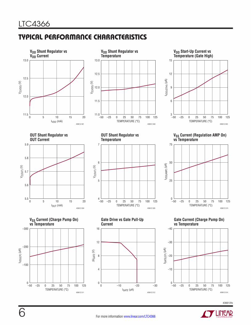
VSS Current (Regulation AMP On) vs Temperature
VDD Shunt Regulator vs VDD Current
VDD Shunt Regulator vs Temperature
VDD Start-Up Current vs Temperature (Gate High)
OUT Shunt Regulator vs OUT Current
OUT Shunt Regulator vs Temperature
IVDD (mA)0
V Z(V
DD) (
V)
13.0
12.5
12.0
11.55
436612 G01
10 15 20TEMPERATURE (°C)
–50
V Z(V
DD) (
V)
13.0
11.0500 10025–25 75
436612 G02
125
12.5
12.0
11.5
TEMPERATURE (°C)
I VDD
(STH
I) (µ
A)
15
12
9
6
3
436612 G03
–50 500 10025–25 75 125
IOUT (mA)
V Z(O
UT) (
V)
5.9
5.8
5.7
5.6
5.5
436612 G04
0 5 10 15 20 –50 500 10025–25 75 125TEMPERATURE (°C)
V Z(O
UT) (
V)
7
6
5
4
436612 G05TEMPERATURE (°C)
I VSS
(AM
P) (µ
A)
75
50
25
0
436612 G10
–50 500 10025–25 75 125
TYPICAL PERFORMANCE CHARACTERISTICS
VSS Current (Charge Pump On) vs Temperature
Gate Drive vs Gate Pull-Up Current
Gate Current (Charge Pump On) vs Temperature
I GAT
E(CP
) (µA
)
–40
–30
–20
–10
0
436612 G14TEMPERATURE (°C)
–50 500 10025–25 75 125TEMPERATURE (°C)
I VSS
(CP)
(µA)
–300
–200
–100
0
436612 G11
–50 500 10025–25 75 125IGATE (µA)
0
∆VGA
TE (V
)
16
12
8
4
0–10 –20
436612 G12
–30
LTC4366
436612fe
For more information www.linear.com/LTC4366 7
TYPICAL PERFORMANCE CHARACTERISTICS
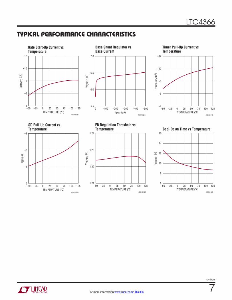
Gate Start-Up Current vs Temperature
I GAT
E(ST
) (µA
)
–12
–10
–8
–6
–4
436612 G15TEMPERATURE (°C)
–50 500 10025–25 75 125
Base Shunt Regulator vs Base Current
Timer Pull-Up Current vs Temperature
I TIM
ER(U
P) (µ
A)
–12
–10
–8
–6
–4
436612 G18TEMPERATURE (°C)
–50 500 10025–25 75 125IBASE (µA)
0
V Z(B
ASE)
(V)
7.0
6.5
6.0
5.5–100
436612 G16
–200 –300 –400 –500
SD Pull-Up Current vs Temperature
TEMPERATURE (°C)
I SD
(µA)
–3
–2
–1
0
436612 G21
–50 500 10025–25 75 125
FB Regulation Threshold vs Temperature Cool-Down Time vs Temperature
V FB(
REG)
(V)
1.24
1.23
1.22
1.21
436612 G22TEMPERATURE (°C)
–50 500 10025–25 75 125TEMPERATURE (°C)
t D(C
OOL)
(s)
16
10
12
14
6
8
436612 G23
–50 500 10025–25 75 125
LTC4366
436612fe
For more information www.linear.com/LTC43668
PIN FUNCTIONSBASE: Base Driver Output for External PNP Shunt Regula-tor. This pin is connected to the anode of an internal 6.2V Zener with the cathode tied to OUT. In cases where lower Zener (Z3) clamp current is desired but a large VSS resis-tor is prohibited, connect an external PNP base to this pin (PNP collector is grounded, emitter is tied to VSS). Tie this pin to VSS if unused.
Exposed Pad: The exposed pad may be left open or con-nected to VSS.
FB: Overvoltage Regulation Amplifier Feedback Input. Connect this pin to an external resistive divider from OUT to ground. The overvoltage regulation amplifier controls the gate of the external N-channel MOSFET to regulate the FB pin voltage at 1.23V below OUT. The overvoltage amplifier will activate a 200mA pull-down on the GATE pin during a fast overvoltage event.
GATE: Gate Drive for External N-Channel MOSFET. Dur-ing start-up an internal 7.5µA current source charges the gate of the external N-channel MOSFET from the VDD pin. Once the OUT voltage is above VSS by 4.75V, the charge pump will finish charging the GATE to 12V above OUT. During a fast overvoltage event, a 200mA pull-down cur-rent source between GATE and OUT is activated, followed by regulation of the GATE pin voltage by the overvoltage regulation amplifier.
OUT: Charge Pump and Overvoltage Regulation Amplifier Supply Voltage. Supply input for floating circuitry powered from the MOSFET source. Once the OUT voltage is 4.75V (UVLO2) above VSS, the charge pump will turn on and draw power from this pin. When OUT exceeds 2.55V (UVLO1) it is used as a power supply and reference input for over-voltage regulation amplifier. This pin is clamped at 5.7V and requires a 0.22µF or greater bypass to the VSS pin.
SD: Shutdown Comparator Input. Tie to VDD if unused. Connect pin to a limited current pull down created by adding a resistor in series with an open-drain or open-collector pull-down transistor. Activating the external pull down overcomes the internal 1.6µA pull-up current source and allows the SD pin to cross the shutdown threshold. This threshold is defined as 1.5V below VDD with a 280mV hysteresis. To prevent false triggers this pin must stay below the threshold for 700µs to activate the shutdown state. The shutdown state lowers the total quiescent cur-rent (IVDD plus IOUT) below 20µA. This quiescent current does not include shunt current in the VDD, OUT and BASE regulators. After a fault on the LTC4366, putting the part in shutdown will clear the fault and allow operation to resume. Clearing the fault during the 9-second cool-down period will shorten the timeout for the LTC4366-2 (auto-retry) version.
TIMER: Timer Input. Leave this pin open for a 1µs overvolt-age regulation period before fault off. Connect a capacitor between this pin and VSS to set a 311ms/µF duration for overvoltage regulation before the switch is turned off. The LTC4366-2 version will restart after a nine second cool-down period.
VDD: Start-Up Supply. Supply input for 7.5µA start-up cur-rent source that charges the gate of the external N-channel MOSFET. Also provides supply for timer and logic circuits active when the external MOSFET is off. This pin is clamped at 12V above VSS. Do not bypass this pin with a capacitor.
VSS: Device Return and Substrate. The capacitors on the TIMER and OUT pins should be returned to this pin.

LTC4366
436612fe
For more information www.linear.com/LTC4366 9
SIMPLIFIED DIAGRAM
FUNCTIONAL DIAGRAM
–+
RFB1
RFB2
436612 SDRSSRSSRSS
CPZ112V
7.5µA20µA
Z35.7V
Z35.7V
RIN
1.23V +–
+–
CHARGEPUMP
f = 2MHz
UVLO24.75V
M1
OUT
FB
GATE OUTVDD
SD
D17.5µA 20µA
OVERVOLTAGEAMPLIFIER
LOGICSUPPLY
VCC
OUTZ112V
LOGICAND
TIMER
SHUTDOWNCOMPARATOR
+–
TIMERCOMPARATOR
UVLO12.55V
Z26.2V
Z35.7V
Z412V
2.8V
VCC
VCCVDD
9µA
TIMER
BASE VSS
1.8µA
1.6µA
CG
VOUT
CT
RFB1
RGRIN
VIN
RFB2
RSS
436612 FD
C1
+–
1.5V+–1.23V +–
–+
Start Run Regulate

LTC4366
436612fe
For more information www.linear.com/LTC436610
OPERATIONThe Simplified Diagram shows three states of operation: the start, run and regulate mode. Previous surge stopper parts are powered off the input supply, therefore the surge voltage is limited to the breakdown voltage of the input pins of the part. As demonstrated in run and regulate modes, the majority of this part is powered off the output, so the MOSFET isolates the surge from the power pins of the part. This allows surge voltages up to the breakdown of the external MOSFET.
In the start mode a 15µA trickle current flows through RIN, half is used to charge the gate with the other half used as bias current. As the GATE pin charges, the external MOSFET brings up the OUT pin. This leads to the run mode where the output is high enough to become a supply voltage for the charge pump. The charge pump is then used to fully charge the gate 12V above the source.
With the output voltage equal to the input voltage, it is necessary to protect the load from an input supply over-voltage. In the regulate mode, the overvoltage regulation amplifier is referenced to the output through a 1.23V reference. If the voltage drop across the upper feedback resistor, RFB1, exceeds 1.23V the regulation amplifier pulls the gate down to regulate the RFB1 voltage back to 1.23V. Therefore, the output voltage is clamped by setting the proper ratio between RFB1 and RFB2.
For example, if the output voltage is regulated at 100V then the voltage drop across the RFB2 is 98.77V. If the Zener Z3 is 5.7V then the voltage drop across RSS is 94.3V. There-fore, when the output is at a high voltage, the majority of the voltage is dropped across the two resistors RFB2 and RSS. This demonstrates how the LTC4366 floats up with the supply. The adjustable 3-terminal regulators, such as the LT®1085 and LM117, are also based on this idea.
The Functional Diagram shows the actual circuits. An external RIN resistor on the VDD pin powers up the 12V shunt regulator which then powers up logic supply, VCC. After verifying that the shutdown input is not active, the GATE pin is charged with a 7.5µA current from VDD. This is the start mode.
Once the OUT to VSS voltage exceeds the 2.55V UVLO1 threshold, the overvoltage amplifier is enabled. Next, the UVLO2 threshold of 4.75V is crossed and the charge pump turns on. The charge pump charges the GATE pin with 20µA to its final value 12V above OUT (clamped by Z4). This allows the capacitor between OUT and VSS to charge until clamped by Z3 to 5.7V. In this run mode the MOSFET is configured as a low resistance pass transistor with little voltage drop and power dissipation in the MOSFET.
The powered up LTC4366 is now ready to protect the load against an overvoltage transient. The overvoltage regula-tion amplifier monitors the load voltage between OUT and ground by sensing the voltage on the FB pin with respect to the OUT pin (drop across RFB1). In an overvoltage condition the OUT rises until the amplifier drives the M1 gate to regulate and limit the output voltage. This is the regulate mode.
During regulation the excess voltage is dropped across the MOSFET. To prevent overheating the MOSFET, the LTC4366 limits the overvoltage regulation time using the TIMER pin. The TIMER pin is charged with 9µA until the pin exceeds 2.8V. At that point an overvoltage fault is set, the MOSFET is turned off, and the part enters a cool-down period of 9 seconds. The logic and timer block are active during cool down while the GATE pin is pulled to OUT.
The latched-off version, LTC4366-1, will remain in fault until the SD pin is toggled low and then high. Once the fault is cleared, the GATE is permitted to turn the MOSFET on again. The auto-retry version, LTC4366-2, waits 9 seconds then clears the fault and restarts.

LTC4366
436612fe
For more information www.linear.com/LTC4366 11
APPLICATIONS INFORMATIONThe typical LTC4366 application is a protected system that distributes power to loads safe from overvoltage transients. External component selection is discussed in the following sections.
Dual Shunt Regulators
The LTC4366 uses two shunt regulators coupled with the external voltage dropping resistors, RSS and RIN, to generate internal supply rails at the VDD and OUT pins. These shunt-regulated rails allow overvoltage protection from unlimited high voltage transients irrespective of the voltage rating of the LTC4366’s internal circuitry.
At the beginning of start-up, during shutdown, or after an overvoltage fault, the GATE pin is clamped to the OUT pin thereby shutting off the MOSFET. This allows the VSS and OUT pins to be pulled to ground by output load and RSS. Under this condition the VDD pin is clamped with a 12V shunt regulator to VSS. The full supply voltage minus 12V is then impressed on the RIN resistor which sets the shunt current. The shunt current can be as high as 10mA which is several orders of magnitude higher than the typical 9µA VDD pin quiescent current.
In normal operation the OUT voltage is equal to the input supply. With C1 fully charged IC1 is zero at this point. Under this condition the voltage between the OUT and VSS pins are clamped with a 5.7V shunt regulator. The input supply
voltage minus 5.7V is impressed on RSS. The RSS current is divided into three areas: the 5.7V shunt current, bias current between OUT and VSS and finally the RIN current. The 5.7V shunt current can be as high as 10mA which greatly exceeds the typical OUT (160µA) bias current.
Turn-On Sequence
The voltage between the VDD and VSS pins is shunt regu-lated to 12V after ramping up the input supply. Next, the internally generated supply, VCC, produces a 30µs power-on-reset pulse which clears the fault latch and initializes internal latches. Next, the shutdown comparator determines if the SD pin is externally pulled low, thereby requesting a low bias current shutdown state. Otherwise the external MOSFET, M1, is allowed to turn on.
Turning on the 7.5µA GATE pull-up current source from the VDD pin begins what can be described as a “bootstrapped” method for powering up the MOSFET gate. Once the GATE reaches the VDD pin voltage (minus a Schottky diode), the 7.5µA source loses voltage headroom and stops charging the GATE (middle of waveforms in Figure 2.). The bootstrap method relies on charging C1 to a sufficient voltage after GATE stops increasing. The voltage on C1 is then used as a supply for a charge pump that charges the gate to its final value 12V above OUT. C1 will discharge if the charge pump current exceeds the C1 charging current. If the voltage drops below 4.35V, the charge pump will pause allowing C1 to recharge.
VDD
SD
R1470k
R2100k
OUT
CG10nF
GATE
M1FQA62N25C
SD FB
CT8.2nF
C10.47µF
RFB112.4k
VOUT1.5A(43V CLAMP)
VIN28V
(18V DC TO 250V DC)
RFB2422k
436612 F01RSS46.4k
RG10Ω
RIN324k
Q1MMBT3904
LTC4366-2
TIMER BASEVSS
Figure 1. Typical ApplicationFigure 2. Turn-On Waveforms
VGATE10V/DIV
VOUT10V/DIV
VC15V/DIV
20ms/DIV 436612 TA01b
CHARGE PUMP PAUSE
CHARGE PUMP STARTS
C1 CHARGING
C1 RECHARGING

LTC4366
436612fe
For more information www.linear.com/LTC436612
APPLICATIONS INFORMATIONStarting up with a supply voltage insufficient to charge C1 with large load current may result in overheating the MOSFET and subsequent damage. While the gate and output are ramping the drop across the MOSFET is the input supply minus the output. If the supply is lower than necessary to charge C1, then the output fails to ramp higher than the supply minus the threshold of the MOSFET. This 3V to 5V MOSFET drop with high load current will result in power dissipation without any protection or timeout limit.
Overvoltage Fault
The LTC4366 prevents an overvoltage on the input supply from reaching the load. Normally, the pass transistor is fully on, powering the load with very little voltage drop. As the input voltage increases the OUT voltage increases until it reaches the regulation point (VREG). From that point any further voltage increase is dropped across the MOSFET. Note the MOSFET is still on so the LTC4366 allows un-interrupted operation during a short overvoltage event.
The VREG point is configured with the two FB resistors, RFB1 and RFB2. The regulation amplifier compares the FB pin to a threshold 1.23V below the OUT pin. During regulation the drop across RFB1 is 1.23V, while the remainder of the VREG voltage is dropped across RFB2.
When the output is at the regulation point a timer is started to prevent excessive power dissipation in the MOSFET. Normally the TIMER pin is held low with a 1.8µA pull-down current. During regulation the TIMER pin charges with 9µA. If the regulation point is held long enough for the TIMER pin to reach 2.8V then an overvoltage fault is latched. The equation for setting the timer capacitor is:
CT = 3.2 • t nF / ms[ ]
Depending on which version, the part will cool down and self start (LTC4366-2), or remain latched off until the SD pin activates a shutdown followed by a start-up command (LTC4366-1). The cool-down time is typically nine seconds which provides a very low pulsed power duty cycle.
Starting up with an input supply overvoltage and full load current does increase the power dissipation in the MOSFET well beyond the case for an overvoltage surge. During the gate and output ramp up, the partial supply voltage (at full current) is dropped across the MOSFET. After start-up the normal overvoltage surge (with timeout) occurs before the shutting off the MOSFET. The Design Example section only considers the normal overvoltage surge for safe operating area (SOA) calculations for the MOSFET. Start-up into overvoltage will require additional SOA considerations.
Shutdown
The LTC4366 has a low current (<20µA) shutdown state that turns off the pass FET by tying the GATE and OUT pins together with a switched resistor. In the normal operating condition, the SD pin is pulled up to the VDD pin voltage with a 1.6µA current source. Tie the SD pin to VDD when the shutdown state is not used.
Bringing the SD pin more than 1.5V below VDD pin volt-age for greater than the 700µs filter time activates the shutdown state. This filter time prevents unwanted activa-tion of shutdown during transients. The SD pin is diode clamped 0.7V below VSS which requires current limiting (maximum 10mA) on the pull-down device. One way to limit the current is to connect an external 470k resistor in series with the open-collector pull-down device. Activat-ing the external pull-down overcomes the internal 1.6µA pull-up current source and allows the SD pin to cross the shutdown threshold.

LTC4366
436612fe
For more information www.linear.com/LTC4366 13
APPLICATIONS INFORMATIONFollowing an overvoltage fault, putting the part in shutdown will clear the fault, allowing operation to resume once the LTC4366 leaves shutdown.
Output Short
A sudden short on the output can result in excessive cur-rent into the LTC4366 GATE pin supplied from the gate capacitor, CG. The GATE pin is internally clamped to OUT with a 10V to 12V clamp. If the OUT pin is pulled low while the GATE pin is held up with CG, then the clamp will be damaged trying to discharge CG when clamp voltage is exceeded. One solution is to add a 1k RS resistor in series with CG with a bypass diode as shown in Figure 3. The diode allows the capacitor to function as a bypass for energy coming from the MOSFET drain to gate capacitor during an supply overvoltage.
GATE
DBYPASS
RS1k
CG
436612 F03
RG
M1
LTC4366
OUT
10V TO12V
Figure 3. Output Short Protection
LTC4366
BASE
436612 F04
RSS
VSS
Figure 4. External PNP Option
Resistor Power Ratings
The proper rating for the RSS resistor in Figure 1 must be considered. During an overvoltage event the OUT pin is at regulation voltage (VREG), so the voltage across RSS is VREG minus 5.7V. A small minimum supply voltage reduces the value of RSS. Therefore, large differences between minimum supply voltage and the regulation voltage may require a large power resistor for RSS.
The full supply voltage minus 12V can appear across RIN during the overvoltage cool-down period. Normally the value for RIN is several times larger than RSS which lowers the power and size requirements for this resistor.
External PNP
In some cases the power resistor for RSS may be physically large. A large value RSS (with lower power and size) may be used in conjunction with a PNP as shown in Figure 4. In addition to the 0.8µA sourced from the BASE pin, the base current from the PNP must flow through RSS which will limit the maximum RSS value. In some cases the minimum PNP Beta is as low as 35. The base current becomes 10µA when the VSS current is 350µA. One can see this allows a 35 (Beta) times larger RSS than the ap-plication without the PNP.
Minimum Supply Start-Up
When designing for the minimum supply condition, it is important that RSS and RIN are chosen to provide enough current to sufficiently charge C1 to 4.75V. The parameters that determine the minimum supply voltage include: C1 voltage, MOSFET threshold voltage, a series Schottky diode voltage drop, resistance of RSS and RIN, current in the VDD

LTC4366
436612fe
For more information www.linear.com/LTC436614
APPLICATIONS INFORMATIONpin, and finally the current from the VSS pin (see Figure 5).
VIN(MIN) = (IVDD • RIN) + VD + VTH + VC1 + (IVSS • RSS)
Using the Electrical Characteristics table for above parameters:
VC1 = VUVLO2 = 4.75V (UVLO2 threshold)
IVDD = IVDD(STHI) = 9µA (IVDD start-up, gate high)
IVSS = IVSS(AMP) = 45µA (IVSS w/regulation amp)
VD = 0.58V
VIN(MIN) = (9µA • RIN) + 0.58V + VTH + 4.75V + (45µA • RSS)
When the MOSFET gate is fully enhanced, the OUT pin voltage is equal to the supply voltage. This places another constraint on the minimum supply voltage because the charge pump increases the VSS current to 160µA. The C1 voltage is assumed to be clamped at 5.7V. These values are specified as VZ(OUT) and IVSS(CP) (charge pump on) in the table of Electrical Characteristics:
VIN(MIN) = VZ(OUT) + (IVSS(CP) • RSS)
or
VIN(MIN) = 5.7V + (160µA • RSS)
The last VIN(MIN) equation sets the maximum value for RSS. After choosing RSS the maximum value for RIN (for that particular RSS) is calculated from the first VIN(MIN) equation:
RSS(MAX) =VIN(MIN) – 5.7V
160µA
RIN(MAX) =VIN(MIN) – 4.75V – 0.58V – VTH – 45µA •RSS( )
9µA
These two equations maximize the values of RSS and RIN (reducing power dissipation) while still providing the necessary VC1 voltage to turn the charge pump on. Increasing the supply voltage beyond the minimum sup-ply voltage increases the current and power in RSS while reducing the time required to charge C1. Conditions that may require an even smaller RSS(MAX) will be discussed in the Maximum Supply Start-Up section.
Maximum Supply Start-Up
The maximum overvoltage supply may also exist during start-up. The overvoltage protection circuitry has to wake up before high voltage is passed to the load. Dynamically the GATE is ramping up while C1 is charging. Capacitor C1 must charge to the 2.55V UVLO1 threshold to turn on the regulation amplifier and reference before the OUT pin voltage exceeds the overvoltage regulation point, VREG. These conditions may reduce the value of RSS below the maximum value dictated by the minimum supply start-up discussed above.
When current in RSS exceeds the current sourced from the VSS pin (essentially IRIN), the capacitor C1 begins to charge. The voltage at the VSS pin when IRIN = IRSS is now labeled VSS(MATCH). The VSS pin voltage is the center of a voltage divider between RIN and RSS after the Zener clamp voltage from VDD to VSS is subtracted from the supply.
VSS(MATCH) = RSS
RSS +RIN• VIN(MAX) – VZ(VDD)( )
As VIN increases the VSS(MATCH) voltage increases. If the match voltage exceeds the overvoltage regulation point (VREG), then load is unprotected. This is true because C1 will still need to charge to 2.55V while VSS already
M1GATED17.5µA
CG
VDD
RINIRIN
VIN
Z35.7V
Z112V
IBIASISHUNT29µAISHUNT1 IC1
IRSS
VOUTOUT
RLOAD
436612 F05
RSS
VSS
CIRCUITSLOGICTIMER
VC1C1+–
Figure 5. Simplified Block Diagram

LTC4366
436612fe
For more information www.linear.com/LTC4366 15
APPLICATIONS INFORMATIONhas exceeded VREG. Since the OUT pin voltage is at least 2.55V larger than VSS it exceeds the specified maximum. Choosing the match point (with supply at the maximum) sufficiently below VREG (by at least 2.55V), allows C1 to charge up in time to protect the load from overvoltage. In reality having VSS pin voltage 7V below VREG provides required margin for charging C1.
VSS(MATCH)(MAX) = VREG – 7V
Increasing RSS increases the match point, so determin-ing the maximum RSS value while still protecting from overvoltage is useful. Using IRIN = IRSS:
RSS = RIN • VRSS
VRIN
Using:
VRSS = VSS(MATCH)(MAX) = VREG – 7V
VRIN = VIN – VZ(VDD) – VRSS
Substituting:
RSS(MAX) =RIN • VREG – 7V( )
VIN(MAX) – 12V – VREG – 7V( )
RSS(MAX) =RIN • VREG – 7V( )
VIN(MAX) – 5V – VREG
If we guarantee that RSS < RSS(MAX) then the following is true:
VSS(MATCH) < VSS(MATCH)(MAX)
C1 bypasses the charge pump, and requires at least a 0.22µF. The size of C1 needs limits also. The gate capaci-tor (CG) dictates the maximum output capacitor C1(MAX) that will charge to the 2.55V UVLO1 threshold (VUVLO1) before the OUT voltage exceeds the overvoltage threshold.
C1(MAX ) =–CG • RSS +RIN( ) VREG – VSS(MATCH)( )
IG •RSS •RIN •In 1–2 • VUVLO1
VREG – VSS(MATCH)
In most cases:
C1(MAX) = 10 • CG to 100 • CG
GATE Capacitor, CG
The gate capacitor is used for three functions. First, CG absorbs charge from the gate-to-drain capacitance of the MOSFET during overvoltage transients. Second, the capacitor also acts as a compensation element for the overvoltage regulation amplifier. The minimum value for CG to guarantee stability is 2nF. Finally, CG sets the slew rate of the GATE and OUT pins. The voltage at the GATE pin rises at a slope equal to 20µA/CG. This slope determines the charging current into the load capacitor.
IINRUSH =
CLOADCG
•IG
The voltage rating for CG must be greater than the regula-tion voltage (VREG).
MOSFET Selection
The LTC4366 drives an N-channel MOSFET to conduct the load current. The important features of the MOSFET are on-resistance, RDS(ON), the maximum drain-source voltage, V(BR)DSS, the threshold voltage, and the SOA.
The maximum allowable drain-source voltage must be higher than the supply voltage. If the output is shorted to ground or during an overvoltage event, the full supply voltage will appear across the MOSFET.
The threshold voltage of the MOSFET is used in the mini-mum supply start-up calculation. For applications with supplies less than 12V, a logic-level MOSFET is required. Above 12V a standard threshold N-channel MOSFET is sufficient.
The SOA of the MOSFET must encompass all fault condi-tions. In normal operation the pass transistor is fully on, dissipating very little power. But during overvoltage faults, the GATE pin is servoed to regulate the output voltage through the MOSFET. Large current and high voltage drop across the MOSFET can coexist in these cases. The SOA curves of the MOSFET must be considered carefully along with the selection of the fault timer capacitor.

LTC4366
436612fe
For more information www.linear.com/LTC436616
APPLICATIONS INFORMATIONLayout Considerations
Due to the high impedances on the SD, VDD, and GATE pins, these pins are susceptible to leakages to ground. For example, a leakage to ground on SD will activate the shutdown state if greater than 1.6µA. Providing adequate spacing away from grounded traces and adding conformal coating on exposed pins lowers the risk that leakage cur-rent will interrupt system operation.
It is important to put the bypass capacitor, C1, as close as possible to the OUT and VSS pins. Place the 10Ω resistor as close as possible to the MOSFET gate pin. This will limit the parasitic trace capacitance that leads to MOSFET self-oscillation.
The FB pin is sensitive to parasitic capacitance when the regulation loop is closed. One result from this capacitive loading is output oscillations during overvoltage regula-tion. It is suggested that the resistors RFB1 and RFB2 be placed close to the pin and that the FB trace itself be minimized in size.
DESIGN EXAMPLE
Overview
The design process starts with minimum input voltage start-up equations to calculate values for RSS and RIN. These values need further refinement to meet two other conditions: the maximum input voltage start-up condi-tions and proper current for the charging of C1. The the remaining element values are calculated based on the input parameters.
Following are the input parameters for this example:
VSUPPLY(MIN) = 18V, VREG = 43V, VIN(MAX) = 250V, ILOAD = 1.5A at start-up, ILOAD = 3A after start-up, VTH = 5V
Important Electrical Characteristics table parameters used in this example are summarized in Table 1.
Step 1: Maximum RSS
In this design example (Figure 6.) the component sizing first considers the start-up phase after the charge pump is active. The goal is to maximize the resistance of RSS which still allows operation when the input voltage is at the minimum value.
VDD
SD
R1470k
R2100k
OUT
CG10nF
GATE
M1FQA62N25C
SD FB
CT8.2nF
C10.47µF
RFB112.4k
VOUT1.5A(43V CLAMP)
VIN28V
(18V DC TO 250V DC)
RFB2422k
436612 F06RSS46.4k
RG10Ω
RIN324k
Q1MMBT3904
LTC4366-2
TIMER BASEVSS
Figure 6. Overvoltage Protected 28V, 1.5A Supply
LTC4366
436612fe
For more information www.linear.com/LTC4366 17
APPLICATIONS INFORMATION
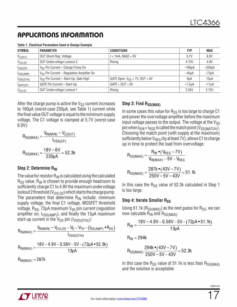
After the charge pump is active the VSS current increases to 160µA (worst-case 230µA, see Table 1) current while the final value OUT voltage is equal to the minimum supply voltage. The C1 voltage is clamped at 5.7V (worst-case 6.0V):
RSS(MAX) =VIN(MIN) – VZ(OUT)
IVSS(CP)
RSS(MAX) = 18V – 6V230µA
= 52.3k
Step 2: Determine RIN
The value for resistor RIN is calculated using the calculated RSS value. RIN is chosen to provide enough headroom to sufficiently charge C1 to 4.9V the maximum undervoltage lockout 2 threshold (VUVLO2) which starts the charge pump. The parameters that determine RIN include: minimum supply voltage, the final C1 voltage, MOSFET threshold voltage, RSS, 72µA maximum VSS pin current (regulation amplifier on, IVSS(AMP)), and finally the 13µA maximum start-up current in the VDD pin (IVDD(STHI)):
RIN(MAX) =VIN(MIN) – VUVLO2 − VD − VTH − ISS(AMP) •RSS( )
IVDD(STHI)
RIN(MAX) =18V − 4.9V − 0.58V − 5V − 72µA • 52.3k( )
13µA
RIN(MAX) = 287k
Table 1. Electrical Parameters Used in Design Example
SYMBOL PARAMETER CONDITIONS TYP MAX
VZ(OUT) OUT Shunt Reg. Voltage I = 1mA, BASE = 0V 5.7V 6.0V
VUVLO2 OUT Undervoltage Lockout 2 Rising 4.75V 4.9V
IVSS(CP) VSS Pin Current – Charge Pump On –160µA –230µA
IVSS(AMP) VSS Pin Current – Regulation Amplifier On –45µA –72µA
IVDD(STHI) VDD Pin Current – Start-Up, Gate High GATE Open, VDD = 7V, OUT = 0V 9µA 13µA
IGATE(ST) GATE Pin Current – Start-Up GATE = OUT = 0V –7.5µA –11µA
VUVLO1 OUT Undervoltage Lockout 1 Rising 2.55V 2.75V
Step 3: Find RSS(MAX)
In some cases this value for RSS is too large to charge C1 and power the overvoltage amplifier before the maximum input voltage passes to the output. The voltage at the VSS pin when IRIN = IRSS is called the match point (VSS(MATCH)). Choosing the match point (with supply at the maximum) sufficiently below VREG (by at least 7V), allows C1 to charge up in time to protect the load from overvoltage:
RSS(MAX) =RIN • VREG – 7V( )
VIN(MAX) − 5V − VREG
RSS(MAX) =287k • 43V – 7V( )250V – 5V – 43V
= 51.1k
In this case the RSS value of 52.3k calculated in Step 1 is too large.
Step 4: Iterate Smaller RSS
Using 51.1k (RSS(MAX)) as the next guess for RSS, we can now calculate RIN and RSS(MAX):
RIN =18V – 4.9V − 0.58V − 5V − 72µA • 51.1k( )
13µA
RIN = 294k
RSS(MAX)294k • 43V – 7V( )250V – 5V − 43V
= 52.3k
In this case the RSS value of 51.1k is less than RSS(MAX) and the solution is acceptable.

LTC4366
436612fe
For more information www.linear.com/LTC436618
Step 5: Determine CG, C1(MAX), Check RSS
The gate capacitor (CG) determines the gate slew rate and therefore the slew rate of the OUT pin since the output voltage follows the GATE pin. The voltage at the GATE pin rises with a slope equal to 7.5µA/CG at startup and 20µA/CG when the charge pump is on. Limiting this slope will limit the inrush current charging the load capacitance where:
IINRUSH = CLOAD
CG•IG
In this example we choose CG to be 10nF which limits the inrush current to be 660mA for a 330µF CLOAD.
C1 is used as a bypass capacitor for the circuitry between the OUT and VSS pins. C1 also stabilizes the shunt regula-tor that clamps the voltage between these pins where the minimum value for regulator stability is 0.22µF. An even greater 0.47µF value is desired for C1 to protect the OUT to VSS circuitry from transients on the OUT pin.
The startup into an overvoltage creates an upper bound-ary on the value of C1. The value of CG, RSS and RVIN determines a maximum C1 that will reach UVLO1 and power the regulation amplifier before the OUT pin voltage exceeds the overvoltage threshold. If our desired value for C1 (0.47µF) exceeds the maximum allowed C1 then a smaller RSS must be used to iterate a new solution for C1(MAX). We start with calculating VSS(MATCH):
VSS(MATCH) = RSS
RSS +RVIN• VIN – VZ(VDD)( )
If we use the worst-case 1% maximum value for RSS (51.6k) and minimum value for RVIN (291k):
VSS(MATCH) = 35.8V
C1(MAX) =–CG • RSS +RIN( ) VREG – VSS(MATCH)( )
IG •RSS •RIN •In 1– 2 • VUVLO1VREG – VSS(MATCH)
Use the worst-case maximum gate current of 11µA instead of the typical 7.5µA and the worst-case minimum UVLO1
APPLICATIONS INFORMATIONthreshold, 2.75V:
C1(MAX ) =–10nF • 51.6k + 291k( ) 43V – 35.8V( )
11µA • 51.6k • 291k •In 1– 2 • 2.75V43V − 35.8V
or
C1(MAX) = 0.1µF
This limit on C1 does not meet the shunt regulator stability requirements (C1 > 0.22µF).
If we desire a larger value of C1 then a lower size of RSS is required. A lower value for RSS is 48.7k, which calls out an RIN value of 309k and a max C1 value of 0.27µF. The next lower value of 46.4k with RVIN of 324k, results in the worst-case maximum C1 value of 0.49µF. A larger C1 increases circuit immunity to transients in exchange for slightly higher current. Therefore, a selection of com-ponents that allow a 0.47µF C1 is recommended.
The lowered RSS value of 46.4k now considers the toler-ances of all the components that set the C1 ramp rate to guarantee it charges to the 2.55V UVLO1 threshold before the OUT voltage exceeds the overvoltage threshold.
Step 6: Determine RFB1, RFB2
The feedback resistors, RFB1 and RFB2, are chosen to regulate the overvoltage at 43V. One way to quickly choose these resistors is to assign 100µA or 1.2V across a 12.4k RFB1. RFB2 would need to drop the remainder of the regu-lated voltage. Dividing this remainder by 100µA yields the value for RFB2. In this example RFB2 drops 41.8V. When divided by 100µA it results in a 422k value.
Step 7: Determine CT, R1
During an overvoltage the power dissipated in the MOSFET is dependent on the load current and the difference be-tween the supply and regulated voltages. It is necessary to keep the device power in a safe range. In the power MOSFET data sheets there is a maximum safe operating curve displaying current versus drain to source voltage for a fixed pulsed time. Other pulsed time data from DC to 10µs are plotted on the one graph. The different lines of operation generally follow a constant power squared

LTC4366
436612fe
For more information www.linear.com/LTC4366 19
APPLICATIONS INFORMATION
VDD
SD
R1470k
R2100k
OUT
CG2nF
GATE
M1IXTH12N100L
SD FB
CT3.3nF
C10.47µF
RFB112.4k
VOUT0.5A(200V CLAMP)
VIN160V (RECTIFIED 110V AC)
100V TO 800V
RFB22M
436612 F07RSS412k
RG10Ω
RIN4.64M
Q1BF722
LTC4366-2
TIMER BASEVSS
DANGER! Lethal Voltages Present
Figure 7. Rectified 110V AC Supply Protected from 220V AC
times time or P2t. Knowing the power we then adjust the time using the timer capacitor to limit the P2t during overvoltage. In this example the MOSFET data sheet has a 6400W2s P2t for a 10ms single pulse.
In this application 250V minus 43V is applied across the MOSFET at 3A. If the power is applied for less than 16.5ms then MOSFET P2t limit is not exceeded:
P = (250V – 43V) • 3A = 621W
P2t = (621W)2 • 16.5ms = 6363W2s
Prior to the moment when the output is regulated at 43V, the output is ramping from 28V to 43V. This ramp time is based on the 20µA gate current charging the 10nF capaci-tor. Using the equation for ramp time:
∆t =
CG • ∆VIG
= 10nF • 15V20µA
= 7.5ms
To be safe we set the overvoltage time to 10ms. We set the regulation time to be 2.5ms (the remainder of the 10ms overvoltage time minus the ramp time). In this example it is assumed the 250V overvoltage is a constant DC volt-age for 10ms. This duration exceeds Mil-Std-1275 which specifies a 70µs surge to 250V that decays in 1.6ms. Us-ing the following equation (based on charging with 9µA) to set the CT:
CT = IT •
∆t∆V
= 9µA •2.5ms2.8V
≈ 8.2nF
In order to limit the SD pin current (10mA max) a collector resistor, R1, in series with Q1 is required. The maximum value for this resistor is around 5M. This requirement oc-curs when the pull-down is required to sink 1.6µA from SD and VDD is clamped at 12V. High valued resistors are susceptible to leakage currents so we chose a 470k resistor for R1. Resistor R2 provides ESD protection for Q1’s base.
The gate resistor RG limits the parasitic trace capacitance on M1’s gate node that could lead to parasitic MOSFET self-oscillation. The recommended value for RG is 10Ω.
High Voltage Application
In Figure 7 the circuit accepts 110V AC (rectified to 160V) and protects the load from accidental connection to 220V AC by limiting the output to less than 200V. The circuit has a 100V to 800V VIN operating range where the FET breakdown voltage limits the maximum input voltage. The C1 is set to 0.47µF to provide a bypass for the charge pump that is large enough to provide good noise immunity from outside voltage transients. The timer capacitor is sized to give a 1ms overvoltage regulation time that keeps the P2t below the 640W2s specified for this MOSFET.

LTC4366
436612fe
For more information www.linear.com/LTC436620
28V Vehicle Application
The circuit in Figure 8 adds reverse voltage protection to the standard 28V application shown in Figure 6. There are three modes to this circuit: pass FET On when the input is 18V to 41V, clamping the output to 43V when more than 43V appears at the input and finally reverse voltage protection when up to –250V DC is present at the input.
The reverse voltage protection consists of the circuitry inside the dotted box in Figure 8. When a positive voltage is first applied to the input, D3 and the forward biased base-collector junction of Q2 allow the gate of M2 to follow the input voltage minus a two diode drop. During this condition the body diode of M2 is used to transmit power to the LTC4366. Once the LTC4366 is powered up it fully enhances the gate of M1 and M2 (via D1). The M1 and M2 pass FETs then provide a low impedance path to the load. In an overvoltage condition, D1 blocks excessive positive voltage from the input supply passing to the GATE pin of the LTC4366. D4 eliminates current flow through R6 when the input is positive while D3 prevents emitter base breakdown of Q2 when the input is powering up.
During negative input voltages Q2 turns on when current from R6 (via D4) develops a forward diode drop on R5. Q2 then holds the gate of M2 at the input voltage which turns M2 off. This blocks negative input voltages from reaching M1 and the load. D2 prevents damage to the LTC4366’s GATE pin by clamping it at ground when the M2’s gate is negative.
Low Voltage Application
The circuit on the last page (Surge Protected Automotive Supply) starts up with minimum input voltage of 9V. In order to successfully start up at 9V and clamp the output voltage at 18V for input voltages up to 100V the value of RSS has to be small (1.91k). The FET used in this case has a 3V threshold to ease the start-up requirements. The timer capacitor is sized to give a 2.5ms overvoltage regulation time that keeps the P2t below the 420W2s specified for this MOSFET.
VDD
SD
R1470k
R4270k
R2100k
OUT
CG10nF
GATE
M1FQA62N25C
M2FDB33N25
REVERSE VOLTAGEPROTECTION
SD FB
CT8.2nF
C10.47µF
RFB112.4k
VOUT1.5A(43V CLAMP)
VIN18V TO 41V(±250V DC)
RFB2422k
436612 F08RSS46.4k
RG10ΩRIN
324k
Q1MMBT3904
D4BAV3004W
D3BAV3004W
LTC4366-2
TIMER BASEVSS
R5470k
Q2MMBT3904
R6270k
D2BAV3004W
D1BAV3004W
Figure 8. 28V Vehicle Application with Reverse Voltage Protection
APPLICATIONS INFORMATION

LTC4366
436612fe
For more information www.linear.com/LTC4366 21
PACKAGE DESCRIPTIONPlease refer to http://www.linear.com/designtools/packaging/ for the most recent package drawings.
1.50 – 1.75(NOTE 4)
2.80 BSC
0.22 – 0.36 8 PLCS (NOTE 3)
DATUM ‘A’
0.09 – 0.20(NOTE 3)
TS8 TSOT-23 0710 REV A
2.90 BSC(NOTE 4)
0.65 BSC
1.95 BSC
0.80 – 0.90
1.00 MAX0.01 – 0.10
0.20 BSC
0.30 – 0.50 REF
PIN ONE ID
NOTE:1. DIMENSIONS ARE IN MILLIMETERS2. DRAWING NOT TO SCALE3. DIMENSIONS ARE INCLUSIVE OF PLATING4. DIMENSIONS ARE EXCLUSIVE OF MOLD FLASH AND METAL BURR5. MOLD FLASH SHALL NOT EXCEED 0.254mm6. JEDEC PACKAGE REFERENCE IS MO-193
3.85 MAX
0.40MAX
0.65REF
RECOMMENDED SOLDER PAD LAYOUTPER IPC CALCULATOR
1.4 MIN2.62 REF
1.22 REF
TS8 Package8-Lead Plastic TSOT-23
(Reference LTC DWG # 05-08-1637 Rev A)

LTC4366
436612fe
For more information www.linear.com/LTC436622
PACKAGE DESCRIPTIONPlease refer to http://www.linear.com/designtools/packaging/ for the most recent package drawings.
2.00 ±0.10(2 SIDES)
NOTE:1. DRAWING CONFORMS TO VERSION (WECD-1) IN JEDEC PACKAGE OUTLINE M0-229 2. DRAWING NOT TO SCALE 3. ALL DIMENSIONS ARE IN MILLIMETERS4. DIMENSIONS OF EXPOSED PAD ON BOTTOM OF PACKAGE DO NOT INCLUDE MOLD FLASH. MOLD FLASH, IF PRESENT, SHALL NOT EXCEED 0.15mm ON ANY SIDE5. EXPOSED PAD SHALL BE SOLDER PLATED6. SHADED AREA IS ONLY A REFERENCE FOR PIN 1 LOCATION ON THE TOP AND BOTTOM OF PACKAGE
0.40 ±0.10
BOTTOM VIEW—EXPOSED PAD
0.56 ±0.05(2 SIDES)
0.75 ±0.05
R = 0.115TYPR = 0.05
TYP
2.15 ±0.05(2 SIDES)
3.00 ±0.10(2 SIDES)
14
85
PIN 1 BARTOP MARK
(SEE NOTE 6)
0.200 REF
0 – 0.05
(DDB8) DFN 0905 REV B
0.25 ±0.050.50 BSC
PIN 1R = 0.20 OR0.25 × 45°CHAMFER
0.25 ±0.05
2.20 ±0.05(2 SIDES)
RECOMMENDED SOLDER PAD PITCH AND DIMENSIONS
0.61 ±0.05(2 SIDES)
1.15 ±0.05
0.70 ±0.05
2.55 ±0.05
PACKAGEOUTLINE
0.50 BSC
DDB Package8-Lead Plastic DFN (3mm × 2mm)
(Reference LTC DWG # 05-08-1702 Rev B)

LTC4366
436612fe
For more information www.linear.com/LTC4366 23Information furnished by Linear Technology Corporation is believed to be accurate and reliable. However, no responsibility is assumed for its use. Linear Technology Corporation makes no representa-tion that the interconnection of its circuits as described herein will not infringe on existing patent rights.
REVISION HISTORYREV DATE DESCRIPTION PAGE NUMBER
A 1/12 Added Patents Pending statementRevised Figure 4 in Applications Information section
111
B 2/12 Removed reference to overcurrent faults under MOSFET SelectionFixed orientation of M2 in Figure 8
1318
C 8/12 Updated Shutdown current from <20µA to <14µAChanged MOSFET part number and Gate Capacitor value used in the Typical ApplicationAdded MP-grade order information and specificationsAdded negative sign to graphs G12 x-axis and G18, G21 y-axisChanged MOSFET part number in Figure 1 and Figure 6Added section GATE Capacitor, CG
Changed ILOAD current from 5A to 3A in Design ExampleUpdated C1(MAX) values in Step 5 calculations to 0.27µF and worst case 0.49µFUpdated calculated values in Step 7, added supporting textChanged MOSFET part number and GATE capacitor used in Figure 7
11
2, 3, 4, 56, 7
11, 161516181919
D 8/13 Simplified Diagram: Corrected amplifier’s input polarity in Regulate DiagramFunctional Diagram: Added switch in series with TIMER pull-down current
99
E 8/15 Clarified “Ambient” on Operating Temperature Range; raised TJMAX to 150°CTIMER Pin Function: Changed 278ms/µF to 311ms/µFFigures 1, 6, 8: Changed CT to 8.2nF from 10nFIn CT equation, changed constant to 3.2 from 3.5; updated CT calculation
28
11, 16, 2012, 19

LTC4366
436612fe
For more information www.linear.com/LTC436624 LINEAR TECHNOLOGY CORPORATION 2011
LT 0815 REV E • PRINTED IN USALinear Technology Corporation1630 McCarthy Blvd., Milpitas, CA 95035-7417(408) 432-1900 ● FAX: (408) 434-0507 ● www.linear.com/LTC4366
TYPICAL APPLICATIONSurge Protected Automotive 12V Supply
VDD
SD
R1470k
R2100k
OUT
CG2nF
GATE
M1HUF76639S3S
SD FB
CT3.3nF
C10.47µF
RFB112.4k
VOUT4A(18V CLAMP)
VIN12V
(9V TO 100V)
RFB2169k
436612 TA02RSS1.91k
RG10Ω
RIN29.4k
Q1MMBT3904
LTC4366-2
TIMER BASEVSS
RELATED PARTSPART NUMBER DESCRIPTION COMMENTS
LTC1696 Overvoltage Protection Controller ThinSOT™ Package, 2.7V to 28V
LTC2909 Triple/Dual Inputs UV/OV Negative Monitor Pin Selectable Input Polarity Allows Negative and OV Monitoring
LTC2912/LTC2913 Single/Dual UV/OV Voltage Monitor Ads UV and OV Trip Values, ±1.5% Threshold Accuracy
LTC2914 Quad UV/OV Monitor For Positive and Negative Supplies
LTC3827/LTC3827-1 Low IQ, Dual, Synchronous Controller 4V ≤ VIN ≤ 36V, 0.8V ≤ VOUT ≤ 10V, 80µA Quiescent Current
LTC3835/LTC3835-1 Low IQ, Synchronous Step-Down Controller Single Channel LTC3827/LTC3827-1
LT3845 Low IQ, Synchronous Step-Down Controller 4V ≤ VIN ≤ 60V, 1.23V ≤ VOUT ≤ 36V, 120µA Quiescent Current
LTC3850 Dual, 550kHz, 2-Phase Synchronous Step-Down Controller
Dual 180° Phased Controllers, VIN 4V to 24V, 97% Duty Cycle, 4mm × 4mm QFN-28, SSOP-28 Packages
LTC3890 Low IQ, Dual 2-Phase, Synchronous Step-Down Controller
4V ≤ VIN ≤ 60V, 0.8V ≤ VOUT ≤ 24V, 50µA Quiescent Current
LT4256 Positive 48V Hot Swap Controller with Open-Circuit Detect
Foldback Current Limiting, Open-Circuit and Overcurrent Fault Output, Up to 80V Supply
LTC4260 Positive High Voltage Hot Swap Controller with 8-Bit ADC and I2C
Wide Operating Range 8.5V to 80V
LTC4352 Ideal MOSFET ORing Diode External N-Channel MOSFETs Replace ORing Diodes, 0V to 18V
LTC4354 Negative Voltage Diode-OR Controller Controls Two N-Channel MOSFETs, 1.2µs Turn-Off, –80V Operation
LTC4355 Positive Voltage Diode-OR Controller Controls Two N-Channel MOSFETs, 0.4µs Turn-Off, 80V Operation
LT4363 High Voltage Surge Stopper 100V Overvoltage and Overcurrent Protection, Latch-Off and Auto-Retry Options
LTC4365 Window Passer – OV, UV and Reverse Supply Protection Controller
2.5V to 34V Operation, Protects 60V to –40V