
LTC2634 Quad 12-/10-/8-Bit Rail-to-Rail DACs with … TA01 –1 –2 1024 2048 3072 2 VCC = 3V...
30
LTC2634 1 Rev D For more information www.analog.com Document Feedback BLOCK DIAGRAM FEATURES APPLICATIONS DESCRIPTION Quad 12-/10-/8-Bit Rail-to-Rail DACs with 10ppm/°C Reference The LTC ® 2634 is a family of quad 12-, 10- and 8-bit volt- age output DACs with an integrated, high accuracy, low drift 10ppm/°C reference in 16-lead QFN and 10-lead MSOP packages. It has rail-to-rail output buffers and is guaranteed monotonic. The LTC2634-L has a full-scale output of 2.5V, and operates from a single 2.7V to 5.5V supply. The LTC2634-H has a full-scale output of 4.096V, and operates from a 4.5V to 5.5V supply. Each DAC can also operate with an external reference, which sets the full-scale output to the external reference voltage. These DACs communicate via an SPI/MICROWIRE com- patible 3-wire serial interface which operates at clock rates up to 50MHz. Serial data output (SDO), a hardware clear (CLR), and an asynchronous DAC update (LDAC) capability are available in the QFN package. The LTC2634 incorporates a power-on reset circuit. Options are avail- able for reset to zero-scale or reset to mid-scale in internal reference mode, or reset to mid-scale in external refer- ence mode after power-up. Integral Nonlinearity (LTC2634-LZ12) n Integrated Precision Reference 2.5V Full-Scale 10ppm/°C (LTC2634-L) 4.096V Full-Scale 10ppm/°C (LTC2634-H) n Maximum INL Error: ±2.5 LSB (LTC2634-12) n Low Noise: 0.75mV P-P 0.1Hz to 200KHz n Guaranteed Monotonic over – 40°C to 125°C Temperature Range n Selectable Internal or External Reference n 2.7V to 5.5V Supply Range (LTC2634-L) n Ultralow Crosstalk Between DACs (2.4nV•s) n Low Power: 0.6mA at 3V n Power-On Reset to Zero-Scale/Mid-Scale n Double Buffered Data Latches n Tiny 16-Lead 3mm × 3mm QFN and 10-Lead MSOP Packages n Mobile Communications n Process Control and Industrial Automation n Automatic Test Equipment n Portable Equipment n Automotive REGISTER REGISTER REGISTER REGISTER DAC A V OUTA (REFLO) CS/LD SCK ( ) QFN PACKAGE ONLY (LDAC) GND V OUTB V REF DAC D REGISTER REGISTER REGISTER REGISTER DAC B DAC C V REF V OUTD REF V CC V REF V OUTC SWITCH INTERNAL REFERENCE 32-BIT SHIFT REGISTER DECODE CONTROL LOGIC POWER-ON RESET SDI 2634 BD (SDO) (CLR) CODE 0 INL (LSB) 0 1 4095 2634 TA01 –1 –2 1024 2048 3072 2 V CC = 3V INTERNAL REF All registered trademarks and trademarks are the property of their respective owners. Protected by U.S. patents, including 5396245, 5859606, 6891433, 6937178, 7414561.
Transcript of LTC2634 Quad 12-/10-/8-Bit Rail-to-Rail DACs with … TA01 –1 –2 1024 2048 3072 2 VCC = 3V...

LTC2634
1Rev D
For more information www.analog.comDocument Feedback
BLOCK DIAGRAM
FEATURES
APPLICATIONS
DESCRIPTION
Quad 12-/10-/8-Bit Rail-to-Rail DACs with 10ppm/°C Reference
The LTC®2634 is a family of quad 12-, 10- and 8-bit volt-age output DACs with an integrated, high accuracy, low drift 10ppm/°C reference in 16-lead QFN and 10-lead MSOP packages. It has rail-to-rail output buffers and is guaranteed monotonic. The LTC2634-L has a full-scale output of 2.5V, and operates from a single 2.7V to 5.5V supply. The LTC2634-H has a full-scale output of 4.096V, and operates from a 4.5V to 5.5V supply. Each DAC can also operate with an external reference, which sets the full-scale output to the external reference voltage.
These DACs communicate via an SPI/MICROWIRE com-patible 3-wire serial interface which operates at clock rates up to 50MHz. Serial data output (SDO), a hardware clear (CLR), and an asynchronous DAC update (LDAC) capability are available in the QFN package. The LTC2634 incorporates a power-on reset circuit. Options are avail-able for reset to zero-scale or reset to mid-scale in internal reference mode, or reset to mid-scale in external refer-ence mode after power-up.
Integral Nonlinearity (LTC2634-LZ12)
n Integrated Precision Reference 2.5V Full-Scale 10ppm/°C (LTC2634-L) 4.096V Full-Scale 10ppm/°C (LTC2634-H)n Maximum INL Error: ±2.5 LSB (LTC2634-12)n Low Noise: 0.75mVP-P 0.1Hz to 200KHzn Guaranteed Monotonic over –40°C to 125°C
Temperature Rangen Selectable Internal or External Referencen 2.7V to 5.5V Supply Range (LTC2634-L)n Ultralow Crosstalk Between DACs (2.4nV•s)n Low Power: 0.6mA at 3Vn Power-On Reset to Zero-Scale/Mid-Scalen Double Buffered Data Latchesn Tiny 16-Lead 3mm × 3mm QFN and 10-Lead
MSOP Packages
n Mobile Communicationsn Process Control and Industrial Automationn Automatic Test Equipmentn Portable Equipmentn Automotive
REGI
STER
REGI
STER
REGI
STER
REGI
STER
DAC AVOUTA
(REFLO)
CS/LD
SCK
( ) QFN PACKAGE ONLY
(LDAC)
GND
VOUTB
VREF
DAC D
REGI
STER
REGI
STER
REGI
STER
REGI
STER
DAC B DAC C
VREF
VOUTD
REF
VCC
VREF
VOUTC
SWITCHINTERNALREFERENCE
32-BIT SHIFT REGISTER
DECODECONTROLLOGIC
POWER-ONRESET
SDI
2634 BD
(SDO)
(CLR) CODE0
INL
(LSB
)
0
1
4095
2634 TA01
–1
–21024 2048 3072
2VCC = 3VINTERNAL REF
All registered trademarks and trademarks are the property of their respective owners. Protected by U.S. patents, including 5396245, 5859606, 6891433, 6937178, 7414561.
LTC2634
2Rev D
For more information www.analog.com
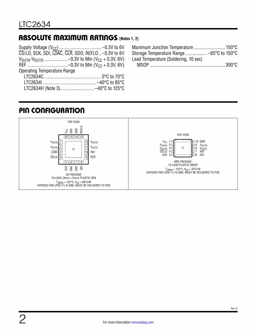
PIN CONFIGURATION
ABSOLUTE MAXIMUM RATINGSSupply Voltage (VCC) ................................... –0.3V to 6VCS/LD, SCK, SDI, LDAC, CLR, SDO, REFLO .. –0.3V to 6VVOUTA-VOUTD ....................–0.3V to Min (VCC + 0.3V, 6V)REF ..................................–0.3V to Min (VCC + 0.3V, 6V)Operating Temperature Range LTC2634C ................................................ 0°C to 70°C LTC2634I .............................................–40°C to 85°C LTC2634H (Note 3) ............................ –40°C to 125°C
(Notes 1, 2)
16 15 14 13
5 6 7 8
TOP VIEW
17
UD PACKAGE16-LEAD (3mm × 3mm) PLASTIC QFN
TJMAX = 125°C, θJA = 68°C/WEXPOSED PAD (PIN 17) IS GND, MUST BE SOLDERED TO PCB
9
10
11
12
4
3
2
1VOUTA
VOUTB
LDAC
CS/LD
VOUTD
VOUTC
REF
CLR
V CC
DNC
GND
REFL
O
SCK
DNC
SDO
SDI
12345
VCCVOUTAVOUTBCS/LD
SCK
109876
GNDVOUTDVOUTCREFSDI
TOP VIEW
MSE PACKAGE10-LEAD PLASTIC MSOP
TJMAX = 125°C, θJA = 35°C/WEXPOSED PAD (PIN 11) IS GND, MUST BE SOLDERED TO PCB
11
Maximum Junction Temperature .......................... 150°CStorage Temperature Range .................. –65°C to 150°CLead Temperature (Soldering, 10 sec) MSOP ............................................................... 300°C
LTC2634
3Rev D
For more information www.analog.com
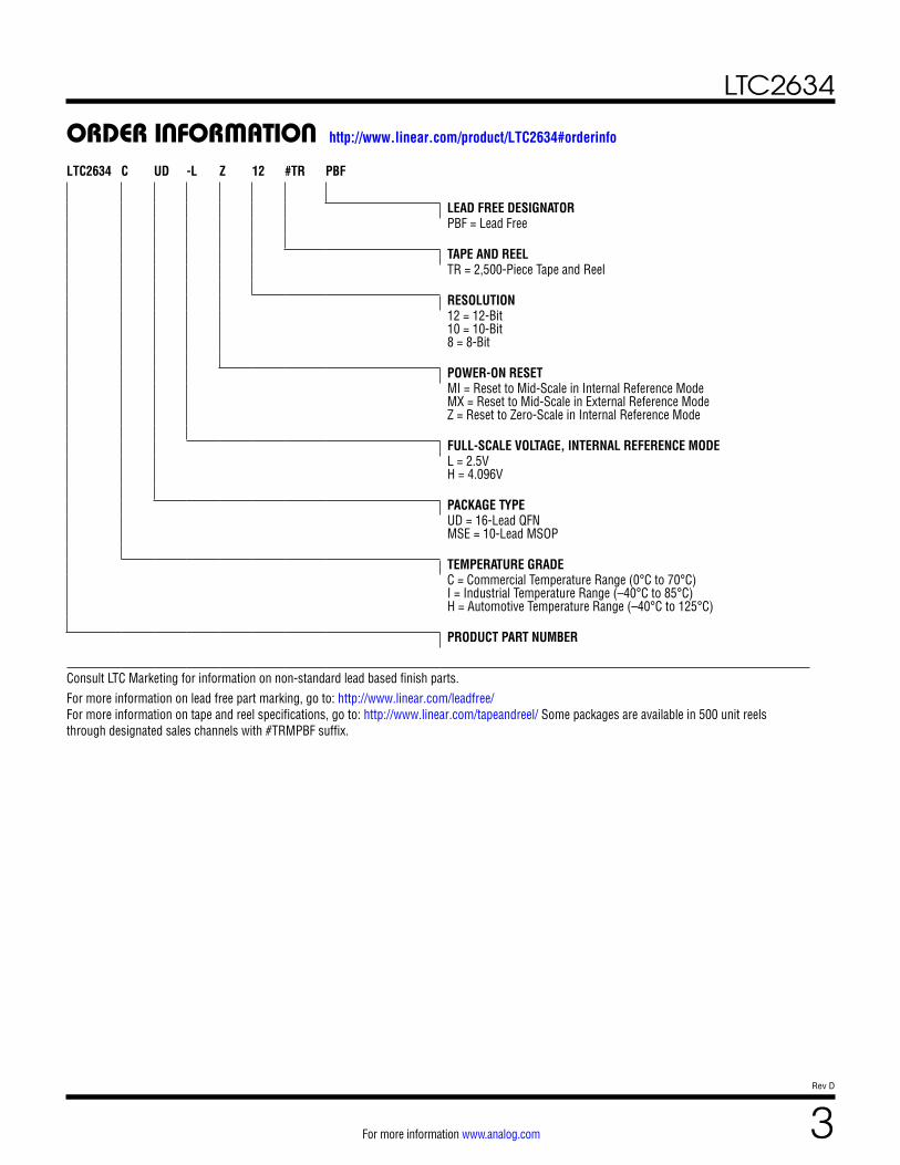
ORDER INFORMATIONLTC2634 C UD -L Z 12 #TR PBF
LEAD FREE DESIGNATORPBF = Lead Free
TAPE AND REELTR = 2,500-Piece Tape and Reel
RESOLUTION12 = 12-Bit 10 = 10-Bit 8 = 8-Bit
POWER-ON RESETMI = Reset to Mid-Scale in Internal Reference Mode MX = Reset to Mid-Scale in External Reference Mode Z = Reset to Zero-Scale in Internal Reference Mode
FULL-SCALE VOLTAGE, INTERNAL REFERENCE MODEL = 2.5V H = 4.096V
PACKAGE TYPEUD = 16-Lead QFN MSE = 10-Lead MSOP
TEMPERATURE GRADEC = Commercial Temperature Range (0°C to 70°C) I = Industrial Temperature Range (–40°C to 85°C) H = Automotive Temperature Range (–40°C to 125°C)
PRODUCT PART NUMBER
Consult LTC Marketing for information on non-standard lead based finish parts.For more information on lead free part marking, go to: http://www.linear.com/leadfree/ For more information on tape and reel specifications, go to: http://www.linear.com/tapeandreel/ Some packages are available in 500 unit reels through designated sales channels with #TRMPBF suffix.
http://www.linear.com/product/LTC2634#orderinfo
LTC2634
4Rev D
For more information www.analog.com
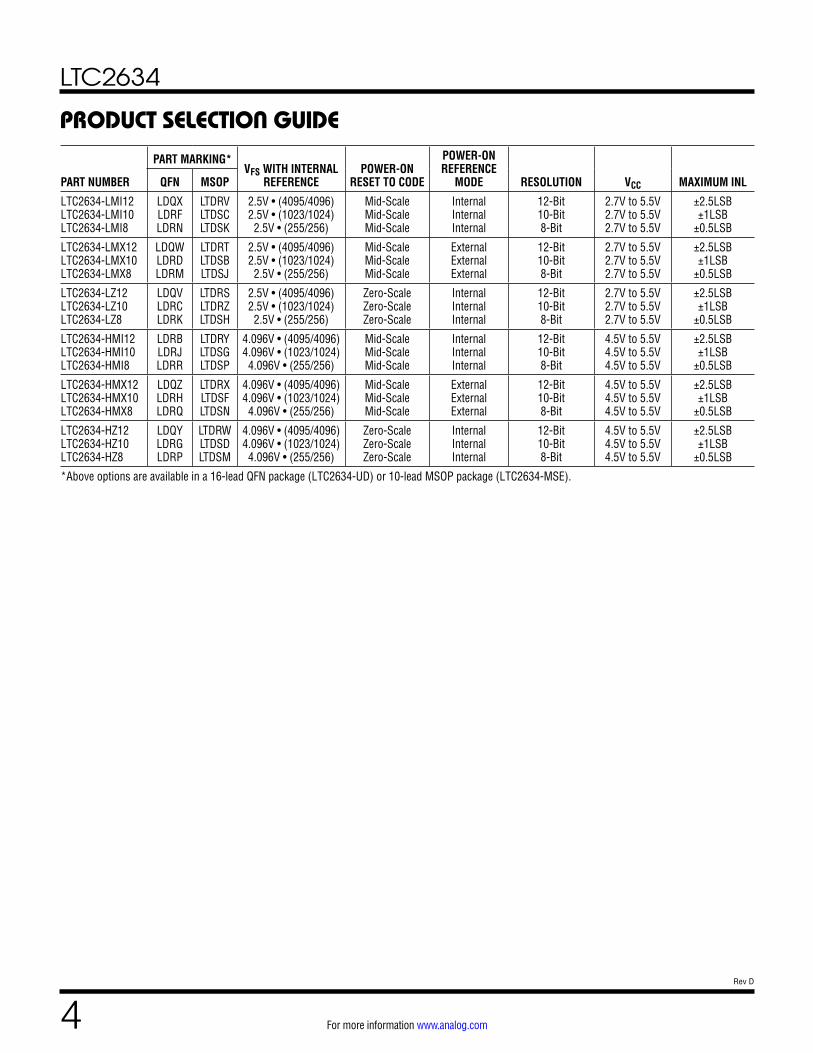
PRODUCT SELECTION GUIDE
PART NUMBER
PART MARKING*VFS WITH INTERNAL
REFERENCEPOWER-ON
RESET TO CODE
POWER-ON REFERENCE
MODE RESOLUTION VCC MAXIMUM INLQFN MSOP
LTC2634-LMI12 LTC2634-LMI10 LTC2634-LMI8
LDQX LDRF LDRN
LTDRV LTDSC LTDSK
2.5V • (4095/4096) 2.5V • (1023/1024) 2.5V • (255/256)
Mid-Scale Mid-Scale Mid-Scale
Internal Internal Internal
12-Bit 10-Bit 8-Bit
2.7V to 5.5V 2.7V to 5.5V 2.7V to 5.5V
±2.5LSB ±1LSB
±0.5LSB
LTC2634-LMX12 LTC2634-LMX10 LTC2634-LMX8
LDQW LDRD LDRM
LTDRT LTDSB LTDSJ
2.5V • (4095/4096) 2.5V • (1023/1024)
2.5V • (255/256)
Mid-Scale Mid-Scale Mid-Scale
External External External
12-Bit 10-Bit 8-Bit
2.7V to 5.5V 2.7V to 5.5V 2.7V to 5.5V
±2.5LSB ±1LSB
±0.5LSB
LTC2634-LZ12 LTC2634-LZ10 LTC2634-LZ8
LDQV LDRC LDRK
LTDRS LTDRZ LTDSH
2.5V • (4095/4096) 2.5V • (1023/1024)
2.5V • (255/256)
Zero-Scale Zero-Scale Zero-Scale
Internal Internal Internal
12-Bit 10-Bit 8-Bit
2.7V to 5.5V 2.7V to 5.5V 2.7V to 5.5V
±2.5LSB ±1LSB
±0.5LSB
LTC2634-HMI12 LTC2634-HMI10 LTC2634-HMI8
LDRB LDRJ LDRR
LTDRY LTDSG LTDSP
4.096V • (4095/4096) 4.096V • (1023/1024)
4.096V • (255/256)
Mid-Scale Mid-Scale Mid-Scale
Internal Internal Internal
12-Bit 10-Bit 8-Bit
4.5V to 5.5V 4.5V to 5.5V 4.5V to 5.5V
±2.5LSB ±1LSB
±0.5LSB
LTC2634-HMX12 LTC2634-HMX10 LTC2634-HMX8
LDQZ LDRH LDRQ
LTDRX LTDSF LTDSN
4.096V • (4095/4096) 4.096V • (1023/1024) 4.096V • (255/256)
Mid-Scale Mid-Scale Mid-Scale
External External External
12-Bit 10-Bit 8-Bit
4.5V to 5.5V 4.5V to 5.5V 4.5V to 5.5V
±2.5LSB ±1LSB
±0.5LSB
LTC2634-HZ12 LTC2634-HZ10 LTC2634-HZ8
LDQY LDRG LDRP
LTDRW LTDSD LTDSM
4.096V • (4095/4096) 4.096V • (1023/1024) 4.096V • (255/256)
Zero-Scale Zero-Scale Zero-Scale
Internal Internal Internal
12-Bit 10-Bit 8-Bit
4.5V to 5.5V 4.5V to 5.5V 4.5V to 5.5V
±2.5LSB ±1LSB
±0.5LSB
*Above options are available in a 16-lead QFN package (LTC2634-UD) or 10-lead MSOP package (LTC2634-MSE).

LTC2634
5Rev D
For more information www.analog.com
ELECTRICAL CHARACTERISTICS The l denotes the specifications which apply over the full operating temperature range, otherwise specifications are at TA = 25°C. VCC = 2.7V to 5.5V, VOUT unloaded unless otherwise specified.LTC2634-LMI12/-LMI10/-LMI8/-LMX12/-LMX10/-LMX8/-LZ12/-LZ10/-LZ8 (VFS = 2.5V)
LTC2634-8 LTC2634-10 LTC2634-12SYMBOL PARAMETER CONDITIONS MIN TYP MAX MIN TYP MAX MIN TYP MAX UNITS
DC Performance
Resolution l 8 10 12 Bits
Monotonicity VCC = 3V, Internal Ref. (Note 4) l 8 10 12 Bits
DNL Differential Nonlinearity VCC = 3V, Internal Ref. (Note 4) l ±0.5 ±0.5 ±1 LSB
INL Integral Nonlinearity VCC = 3V, Internal Ref. (Note 4) l ±0.05 ±0.5 ±0.2 ±1 ±1 ±2.5 LSB
ZSE Zero-Scale Error VCC = 3V, Internal Ref., Code = 0 l 0.5 5 0.5 5 0.5 5 mV
VOS Offset Error VCC = 3V, Internal Ref. (Note 5) l ±0.5 ±5 ±0.5 ±5 ±0.5 ±5 mV
VOSTC VOS Temperature Coefficient
VCC = 3V, Internal Ref. ±10 ±10 ±10 µV/°C
GE Gain Error VCC = 3V, Internal Ref. l ±0.2 ±0.8 ±0.2 ±0.8 ±0.2 ±0.8 %FSR
GETC Gain Temperature Coefficient
VCC = 3V, Internal Ref. (Note 10) C-Grade I-Grade H-Grade
10 10 10
10 10 10
10 10 10
ppm/°C ppm/°C ppm/°C
Load Regulation Internal Ref., Mid-Scale VCC = 3V ±10%, –5mA ≤ IOUT ≤ 5mA
l
0.009
0.016
0.035
0.064
0.14
0.256
LSB/
mA
Internal Ref., Mid-Scale VCC = 5V ±10%, –10mA ≤ IOUT ≤ 10mA
l
0.009
0.016
0.035
0.064
0.14
0.256
LSB/
mA
ROUT DC Output Impedance Internal Ref., Mid-Scale VCC = 3V ±10%, –5mA ≤ IOUT ≤ 5mA
l
0.09
0.156
0.09
0.156
0.09
0.156
Ω
Internal Ref., Mid-Scale VCC = 5V ±10%, –10mA ≤ IOUT ≤ 10mA
l
0.09
0.156
0.09
0.156
0.09
0.156
Ω
SYMBOL PARAMETER CONDITIONS MIN TYP MAX UNITS
VOUT DAC Output Span External Reference Internal Reference
0 to VREF 0 to 2.5
V V
PSR Power Supply Rejection VCC = 3V ±10% or 5V ±10% –80 dB
ISC Short-Circuit Output Current (Note 6) Sinking Sourcing
VFS = VCC = 5.5V Zero-Scale; VOUT Shorted to VCC Full-Scale; VOUT Shorted to GND
l
l
27
–27
48
–48
mA mA
Power Supply
VCC Positive Supply Voltage For Specified Performance l 2.7 5.5 V
ICC Supply Current (Note 7) VCC = 3V, VREF = 2.5V, External Reference VCC = 3V, Internal Reference VCC = 5V VREF = 2.5V, External Reference VCC = 5V, Internal Reference
l
l
l
l
0.5 0.6 0.6 0.7
0.7 0.8 0.8 0.9
mA mA mA mA
ISD Supply Current in Power-Down Mode (Note 7) VCC = 5V, C-Grade, I-Grade VCC = 5V, H-Grade
l
l
0.5 0.5
20 30
µA µA

LTC2634
6Rev D
For more information www.analog.com
ELECTRICAL CHARACTERISTICS The l denotes the specifications which apply over the full operating temperature range, otherwise specifications are at TA = 25°C. VCC = 2.7V to 5.5V, VOUT unloaded unless otherwise specified.LTC2634-LMI12/-LMI10/-LMI8/-LMX12/-LMX10/-LMX8/-LZ12/-LZ10/-LZ8 (VFS = 2.5V)
SYMBOL PARAMETER CONDITIONS MIN TYP MAX UNITS
Reference Input
VREF Input Voltage Range l 1 VCC V
Resistance l 120 160 200 kΩ
Capacitance 14 pF
IREF Reference Current, Power-Down Mode DAC Powered Down l 0.005 1.5 µA
Reference Output
Output Voltage l 1.24 1.25 1.26 V
Reference Temperature Coefficient ±10 ppm/°C
Output Impedance 0.5 kΩ
Capacitive Load Driving 10 µF
Short-Circuit Current VCC = 5.5V, REF Shorted to GND 2.5 mA
Digital I/O
VIH Digital Input High Voltage VCC = 3.6V to 5.5V VCC = 2.7V to 3.6V
l
l
2.4 2.0
V V
VIL Digital Input Low Voltage VCC = 4.5V to 5.5V VCC = 2.7V to 4.5V
l
l
0.8 0.6
V V
VOH Digital Output High Voltage Load Current = –100µA l VCC – 0.4 V
VOL Digital Output Low Voltage Load Current = 100µA l 0.4 V
ILK Digital Input Leakage VIN = GND to VCC l ±1 µA
CIN Digital Input Capacitance (Note 8) l 2.5 pF
AC Performance
tS Settling Time VCC = 3V (Note 9) ±0.39% (±1LSB at 8 Bits) ±0.098% (±1LSB at 10 Bits) ±0.024% (±1LSB at 12 Bits)
3.3 3.8 4.2
µs µs µs
Voltage Output Slew Rate 1.0 V/µs
Capacitive Load Driving 500 pF
Glitch Impulse At Mid-Scale Transition 2.1 nV•s
DAC-to-DAC Crosstalk 1 DAC Held at FS, 1 DAC Switch 0 – FS 2.1 nV•s
Multiplying Bandwidth External Reference 320 kHz
en Output Voltage Noise Density At f = 1kHz, External Reference At f = 10kHz, External Reference At f = 1kHz, Internal Reference At f = 10kHz, Internal Reference
180 160 200 180
nV/√Hz nV/√Hz nV/√Hz nV/√Hz
Output Voltage Noise 0.1Hz to 10Hz, External Reference 0.1Hz to 10Hz, Internal Reference 0.1Hz to 200kHz, External Reference 0.1Hz to 200kHz, Internal Reference CREF = 0.1µF
35 40
680 730
µVP-P µVP-P µVP-P µVP-P

LTC2634
7Rev D
For more information www.analog.com
ELECTRICAL CHARACTERISTICS The l denotes the specifications which apply over the full operating temperature range, otherwise specifications are at TA = 25°C. VCC = 2.7V to 5.5V, VOUT unloaded unless otherwise specified.LTC2634-LMI12/-LMI10/-LMI8/-LMX12/-LMX10/-LMX8/-LZ12/-LZ10/-LZ8 (VFS = 2.5V)
SYMBOL PARAMETER CONDITIONS MIN TYP MAX UNITS
t1 SDI Valid to SCK Setup l 4 ns
t2 SDI Valid to SCK Hold l 4 ns
t3 SCK High Time l 9 ns
t4 SCK Low Time l 9 ns
t5 CS/LD Pulse Width l 10 ns
t6 LSB SCK High to CS/LD High l 7 ns
t7 CS/LD Low to SCK High l 7 ns
t8 CLR Pulse Width l 20 ns
t9 LDAC Pulse Width l 15 ns
t10 CS/LD High to SCK Positive Edge l 7 ns
SCK Frequency 50% Duty Cycle l 50 MHz
t11 CS/LD High to LDAC High or Low Transition l 200 ns
t12 SDO Propagation Delay from SCK Falling Edge CLOAD = 10pF VCC = 4.5V to 5.5V VCC = 2.7V to 5.5V
l
l
20 45
ns ns

LTC2634
8Rev D
For more information www.analog.com
ELECTRICAL CHARACTERISTICS The l denotes the specifications which apply over the full operating temperature range, otherwise specifications are at TA = 25°C. VCC = 4.5V to 5.5V, VOUT unloaded unless otherwise specified.LTC2634-HMI12/-HMI10/-HMI8/-HMX12/-HMX10/-HMX8/-HZ12/-HZ10/-HZ8 (VFS = 4.096V)
LTC2634-8 LTC2634-10 LTC2634-12SYMBOL PARAMETER CONDITIONS MIN TYP MAX MIN TYP MAX MIN TYP MAX UNITS
DC Performance
Resolution l 8 10 12 Bits
Monotonicity VCC = 5V, Internal Ref. (Note 4) l 8 10 12 Bits
DNL Differential Nonlinearity VCC = 5V, Internal Ref. (Note 4) l ±0.5 ±0.5 ±1 LSB
INL Integral Nonlinearity VCC = 5V, Internal Ref. (Note 4) l ±0.05 ±0.5 ±0.2 ±1 ±1 ±2.5 LSB
ZSE Zero-Scale Error VCC = 5V, Internal Ref., Code = 0 l 0.5 5 0.5 5 0.5 5 mV
VOS Offset Error VCC = 5V, Internal Ref. (Note 5) l ±0.5 ±5 ±0.5 ±5 ±0.5 ±5 mV
VOSTC VOS Temperature Coefficient
VCC = 5V, Internal Ref. ±10 ±10 ±10 µV/°C
GE Gain Error VCC = 5V, Internal Ref. l ±0.2 ±0.8 ±0.2 ±0.8 ±0.2 ±0.8 %FSR
GETC Gain Temperature Coefficient
VCC = 5V, Internal Ref. (Note 10) C-Grade I-Grade H-Grade
10 10 10
10 10 10
10 10 10
ppm/°C ppm/°C ppm/°C
Load Regulation VCC = 5V ±10%, Internal Ref., Mid-Scale, –10mA ≤ IOUT ≤ 10mA
l
0.006
0.01
0.022
0.04
0.09
0.16
LSB/
mA
ROUT DC Output Impedance VCC = 5V ±10%, Internal Ref., Mid-Scale, –10mA ≤ IOUT ≤ 10mA
l
0.09
0.156
0.09
0.156
0.09
0.156
Ω
SYMBOL PARAMETER CONDITIONS MIN TYP MAX UNITS
VOUT DAC Output Span External Reference Internal Reference
0 to VREF 0 to 4.096
V V
PSR Power Supply Rejection VCC = 5V ±10% –80 dB
ISC Short-Circuit Output Current (Note 6) Sinking Sourcing
VFS = VCC = 5.5V Zero-Scale; VOUT Shorted to VCC Full-Scale; VOUT Shorted to GND
l
l
27 –27
48 –48
mA mA
Power Supply
VCC Positive Supply Voltage For Specified Performance l 4.5 5.5 V
ICC Supply Current (Note 7) VCC = 5V, VREF = 4.096V, External Reference VCC = 5V, Internal Reference
l
l
0.6 0.7
0.8 0.9
mA mA
ISD Supply Current in Power-Down Mode (Note 7)
VCC = 5V, C-Grade, I-Grade VCC = 5V, H-Grade
l
l
0.5 0.5
20 30
µA µA

LTC2634
9Rev D
For more information www.analog.com
ELECTRICAL CHARACTERISTICS The l denotes the specifications which apply over the full operating temperature range, otherwise specifications are at TA = 25°C. VCC = 4.5V to 5.5V, VOUT unloaded unless otherwise specified.LTC2634-HMI12/-HMI10/-HMI8/-HMX12/-HMX10/-HMX8/-HZ12/-HZ10/-HZ8 (VFS = 4.096V)
SYMBOL PARAMETER CONDITIONS MIN TYP MAX UNITS
Reference Input
VREF Input Voltage Range l 1 VCC V
Resistance l 120 160 200 kΩ
Capacitance 14 pF
IREF Reference Current, Power-Down Mode DAC Powered Down l 0.005 1.5 µA
Reference Output
Output Voltage l 2.032 2.048 2.064 V
Reference Temperature Coefficient ±10 ppm/°C
Output Impedance 0.5 kΩ
Capacitive Load Driving 10 µF
Short-Circuit Current VCC = 5.5V, REF Shorted to GND 4 mA
Digital I/O
VIH Digital Input High Voltage l 2.4 V
VIL Digital Input Low Voltage l 0.8 V
VOH Digital Output High Voltage Load Current = –100µA l VCC – 0.4 V
VOL Digital Output Low Voltage Load Current = 100µA l 0.4 V
ILK Digital Input Leakage VIN = GND to VCC l ±1 µA
CIN Digital Input Capacitance (Note 8) l 2.5 pF
AC Performance
tS Settling Time VCC = 5V (Note 9) ±0.39% (±1LSB at 8 Bits) ±0.098% (±1LSB at 10 Bits) ±0.024% (±1LSB at 12 Bits)
3.8 4.2 4.8
µs µs µs
Voltage Output Slew Rate 1.0 V/µs
Capacitive Load Driving 500 pF
Glitch Impulse At Mid-Scale Transition 3.0 nV•s
DAC-to-DAC Crosstalk 1 DAC Held at FS, 1 DAC Switch 0 – FS 2.4 nV•s
Multiplying Bandwidth External Reference 320 kHz
en Output Voltage Noise Density At f = 1kHz, External Reference At f = 10kHz, External Reference At f = 1kHz, Internal Reference At f = 10kHz, Internal Reference
180 160 250 230
nV/√Hz nV/√Hz nV/√Hz nV/√Hz
Output Voltage Noise 0.1Hz to 10Hz, External Reference 0.1Hz to 10Hz, Internal Reference 0.1Hz to 200kHz, External Reference 0.1Hz to 200kHz, Internal Reference CREF = 0.1µF
35 50
680 750
µVP-P µVP-P µVP-P µVP-P

LTC2634
10Rev D
For more information www.analog.com
ELECTRICAL CHARACTERISTICS The l denotes the specifications which apply over the full operating temperature range, otherwise specifications are at TA = 25°C. VCC = 4.5V to 5.5V, VOUT unloaded unless otherwise specified.LTC2634-HMI12/-HMI10/-HMI8/-HMX12/-HMX10/-HMX8/-HZ12/-HZ10/-HZ8 (VFS = 4.096V)
SYMBOL PARAMETER CONDITIONS MIN TYP MAX UNITS
t1 SDI Valid to SCK Setup l 4 ns
t2 SDI Valid to SCK Hold l 4 ns
t3 SCK High Time l 9 ns
t4 SCK Low Time l 9 ns
t5 CS/LD Pulse Width l 10 ns
t6 LSB SCK High to CS/LD High l 7 ns
t7 CS/LD Low to SCK High l 7 ns
t8 CLR Pulse Width l 20 ns
t9 LDAC Pulse Width l 15 ns
t10 CS/LD High to SCK Positive Edge l 7 ns
SCK Frequency 50% Duty Cycle l 50 MHz
t11 CS/LD High to LDAC High or Low Transition l 200 ns
t12 SDO Propagation Delay from SCK Falling Edge CLOAD = 10pF VCC = 4.5V to 5.5V
l
20
ns
Note 1: Stresses beyond those listed under Absolute Maximum Ratings may cause permanent damage to the device. Exposure to any Absolute Maximum Rating condition for extended periods may affect device reliability and lifetime.Note 2: All voltages are with respect to GND.Note 3: Operating at temperatures above 90°C and with VCC > 4V requires VCC slew rates to be no greater than 73mV/µs.Note 4: Linearity and monotonicity are defined from code kL to code 2N – 1, where N is the resolution and kL is given by kL = 0.016 • (2N/ VFS), rounded to the nearest whole code. For VFS = 2.5V and N = 12, kL = 26 and linearity is defined from code 26 to code 4,095. For VFS = 4.096V and N = 12, kL = 16 and linearity is defined from code 16 to code 4,095. Note 5: Inferred from measurement at code 16 (LTC2634-12), code 4 (LTC2634-10) or code 1 (LTC2634-8), and at full-scale.
Note 6: This IC includes current limiting that is intended to protect the device during momentary overload conditions. Junction temperature can exceed the rated maximum during current limiting. Continuous operation above the specified maximum operating junction temperature may impair device reliability.Note 7: Digital inputs at 0V or VCC.Note 8: Guaranteed by design and not production tested.Note 9: Internal Reference mode. DAC is stepped 1/4 scale to 3/4 scale and 3/4 scale to 1/4 scale. Load is 2kΩ in parallel with 100pF to GND.Note 10: Temperature coefficient is calculated by dividing the maximum change in output voltage by the specified temperature range.
LTC2634
11Rev D
For more information www.analog.com
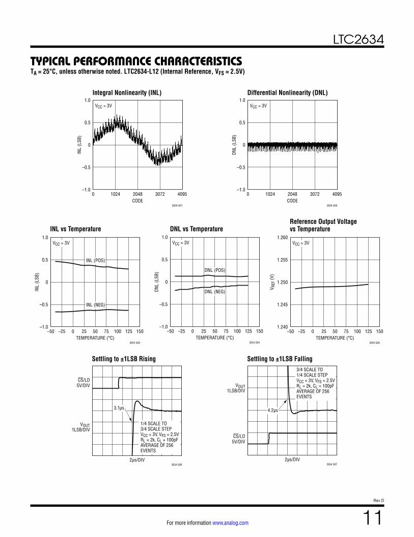
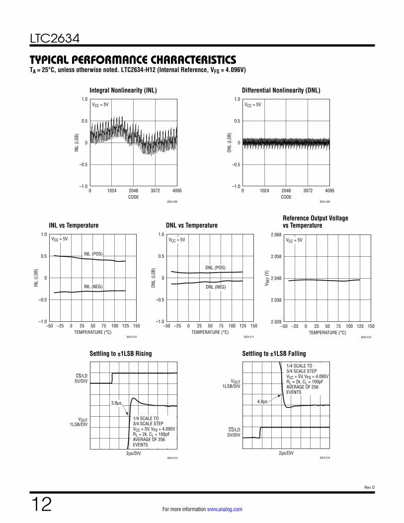
TYPICAL PERFORMANCE CHARACTERISTICS
Integral Nonlinearity (INL) Differential Nonlinearity (DNL)
INL vs Temperature DNL vs TemperatureReference Output Voltage vs Temperature
Settling to ±1LSB Rising Settling to ±1LSB Falling
TA = 25°C, unless otherwise noted. LTC2634-L12 (Internal Reference, VFS = 2.5V)
CODE0
INL
(LSB
)
1.0
0.5
0
–0.5
–1.01024 3072
2634 G01
40952048
VCC = 3V
CODE0
DNL
(LSB
)
1.0
0.5
0
–0.5
–1.01024 3072
2634 G02
40952048
VCC = 3V
TEMPERATURE (°C)–50
INL
(LSB
)
1.0
0.5
0
–0.5
–1.0–25 125100755025
2634 G03
1500
VCC = 3V
INL (POS)
INL (NEG)
TEMPERATURE (°C)–50
DNL
(LSB
)
1.0
0.5
0
–0.5
–1.0–25 125100755025
2634 G04
1500
VCC = 3V
DNL (POS)
DNL (NEG)
TEMPERATURE (°C)–50
V REF
(V)
1.260
1.255
1.250
1.245
1.240–25 125100755025
2634 G05
1500
VCC = 3V
2µs/DIV
CS/LD5V/DIV
VOUT1LSB/DIV
2634 G06
1/4 SCALE TO3/4 SCALE STEPVCC = 3V, VFS = 2.5VRL = 2k, CL = 100pFAVERAGE OF 256 EVENTS
3.1µs
2µs/DIV
CS/LD5V/DIV
VOUT1LSB/DIV
2634 G07
3/4 SCALE TO1/4 SCALE STEPVCC = 3V, VFS = 2.5VRL = 2k, CL = 100pFAVERAGE OF 256 EVENTS
4.2µs
LTC2634
12Rev D
For more information www.analog.com
TYPICAL PERFORMANCE CHARACTERISTICS
Integral Nonlinearity (INL) Differential Nonlinearity (DNL)
INL vs Temperature DNL vs TemperatureReference Output Voltage vs Temperature
Settling to ±1LSB Rising Settling to ±1LSB Falling
TA = 25°C, unless otherwise noted. LTC2634-H12 (Internal Reference, VFS = 4.096V)
CODE0
INL
(LSB
)
1.0
0.5
0
–0.5
–1.01024 3072
2634 G08
40952048
VCC = 5V
CODE0
DNL
(LSB
)
1.0
0.5
0
–0.5
–1.01024 3072
2634 G09
40952048
VCC = 5V
TEMPERATURE (°C)–50
INL
(LSB
)
1.0
0.5
0
–0.5
–1.0–25 125100755025
2634 G10
1500
VCC = 5V
INL (POS)
INL (NEG)
TEMPERATURE (°C)–50
DNL
(LSB
)
1.0
0.5
0
–0.5
–1.0–25 125100755025
2634 G11
1500
VCC = 5V
DNL (POS)
DNL (NEG)
TEMPERATURE (°C)–50
V REF
(V)
2.068
2.058
2.048
2.038
2.028–25 125100755025
2634 G12
1500
VCC = 5V
2µs/DIV
CS/LD5V/DIV
VOUT1LSB/DIV
2634 G13
1/4 SCALE TO3/4 SCALE STEPVCC = 5V, VFS = 4.095VRL = 2k, CL = 100pFAVERAGE OF 256 EVENTS
3.8µs
2µs/DIV
CS/LD5V/DIV
VOUT1LSB/DIV
2634 G14
1/4 SCALE TO3/4 SCALE STEPVCC = 5V, VFS = 4.095VRL = 2k, CL = 100pFAVERAGE OF 256EVENTS
4.8µs

LTC2634
13Rev D
For more information www.analog.com
TYPICAL PERFORMANCE CHARACTERISTICS
Integral Nonlinearity (INL) Differential Nonlinearity (DNL)
LTC2634-10
Integral Nonlinearity (INL) Differential Nonlinearity (DNL)
LTC2634-8
Load Regulation Current Limiting
LTC2634
Offset Error vs Temperature
TA = 25°C, unless otherwise noted
CODE0
INL
(LSB
)
1.0
0.5
0
–0.5
–1.0256 768
2634 G15
1023512
VCC = 3VVFS = 2.5VINTERNAL REF
CODE0
DNL
(LSB
)
1.0
0.5
0
–0.5
–1.0256 768
2634 G16
1023512
VCC = 3VVFS = 2.5VINTERNAL REF
CODE0
INL
(LSB
)
0.50
0.25
0
–0.25
–0.5064 192
2634 G17
255128
VCC = 3VVFS = 2.5VINTERNAL REF
CODE0
DNL
(LSB
)0.50
0.25
0
–0.25
–0.5064 192
2634 G18
255128
VCC = 3VVFS = 2.5VINTERNAL REF
IOUT (mA)–30
∆VOU
T (m
V)
10
8
6
4
2
–6
–4
–2
0
–8
–10–20 20100
2634 G19
30–10
VCC = 5V (LTC2634-H)VCC = 5V (LTC2634-L)VCC = 3V (LTC2634-L)
INTERNAL REF.CODE = MID-SCALE
IOUT (mA)–30
∆VOU
T (V
)
0.20
0.15
0.10
0.05
–0.15
–0.01
–0.05
0
–0.20–20 20100
2634 G20
30–10
VCC = 5V (LTC2634-H)VCC = 5V (LTC2634-L)VCC = 3V (LTC2634-L)
INTERNAL REF.CODE = MID-SCALE
TEMPERATURE (°C)–50
OFFS
ET E
RROR
(mV)
3
2
1
0
–1
–2
–3–25 125100755025
2634 G21
1500

LTC2634
14Rev D
For more information www.analog.com
TYPICAL PERFORMANCE CHARACTERISTICS
Large-Signal Response Mid-Scale Glitch Impulse Power-On Reset Glitch
Headroom at Rails vs Output Current Exiting Power-Down to Mid-Scale Power-On Reset to Mid-Scale
Supply Current vs Logic Voltage Hardware CLR Hardware CLR to Mid-Scale
LTC2634TA = 25°C, unless otherwise noted
2µs/DIV
VOUT0.5V/DIV
2634 G22
VFS = VCC = 5V1/4 SCALE to 3/4 SCALE
2µs/DIV
VOUT5mV/DIV
CS/LD5V/DIV
2634 G23
LTC2634-H12, VCC = 5V3.0nV•s TYP
LTC2634-L12, VCC = 3V2.1nV•s TYP
200µs/DIV
VOUT5mV/DIV
VCC2V/DIV
2636 G24
LTC2634-L
ZERO SCALE
IOUT (mA)0
V OUT
(V)
5.0
4.5
1.0
1.5
2.0
2.5
3.0
3.5
4.0
0.5
01 7 8 96543
2634 G25
102
5V SOURCING
3V (LTC2634-L) SOURCING
3V (LTC2634-L) SINKING
5V SINKING
5µs/DIV
VOUT0.5V/DIV
CS/LD2V/DIV
2634 G26
LTC2634-H
VCC = 5VINTERNAL REF
DACs A-C INPOWER-DOWN
MODE
200µs/DIV
VCC2V/DIV
VOUT0.5V/DIV
2634 G27
LTC2634-H
LTC2634-L
1µs/DIV
CLR5V/DIV
VOUT1V/DIV
2634 G29
VCC = 5VVREF = 4.096VCODE = FULL-SCALE
1µs/DIV
VOUT1V/DIV
CLR5V/DIV
2634 G30
VCC = 5VVREF = 4.096VCODE = FULL-SCALE
LOGIC VOLTAGE (V)0
I CC
(mA)
1.0
1.2
1.4
4
2634 G28
0.8
0.6
0.41 2 3 5
VCC = 5V
VCC = 3V(LTC2634-L)
SWEEP SCK, SDI, CS/LDBETWEEN 0V AND VCC
LTC2634
15Rev D
For more information www.analog.com
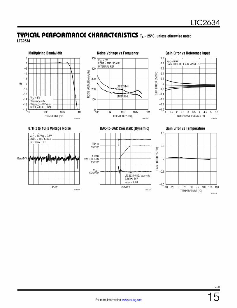
TYPICAL PERFORMANCE CHARACTERISTICS
Mulitplying Bandwidth Noise Voltage vs Frequency Gain Error vs Reference Input
0.1Hz to 10Hz Voltage Noise DAC-to-DAC Crosstalk (Dynamic) Gain Error vs Temperature
LTC2634TA = 25°C, unless otherwise noted
FREQUENCY (Hz)
dB
2636 G31
2
0
–16
–14
–12
–10
–8
–6
–4
–2
–181k 100k 1M10k
VCC = 5VVREF(DC) = 2VVREF(AC) = 0.2VP-PCODE = FULL-SCALE
FREQUENCY (Hz)100
NOIS
E VO
LTAG
E (n
V/√H
z)
500
400
300
200
100
01k 100k
2636 G32
1M10k
VCC = 5VCODE = MID-SCALEINTERNAL REF
LTC2634-H
LTC2634-L
1s/DIV
10µV/DIV
2634 G34
VCC = 5V, VFS = 2.5VCODE = MID-SCALEINTERNAL REF
2µs/DIV
VOUT1mV/DIV
1 DACSWITCH 0-FS
2V/DIV
CS/LD5V/DIV
2634 G35
LTC2634-H12, VCC = 5V2.4nV•s TYPCREF = 0.1µF
TEMPERATURE (°C)–50
GAIN
ERR
OR (%
FSR)
1.0
0.5
0
–0.5
–1.0–25 125100755025
2634 G36
1500
REFERENCE VOLTAGE (V)1
GAI
N ER
ROR
(%FS
R)
1.0
0.8
0.6
0.4
–0.6
–0.8
–0.4
–0.2
0.2
0
–1.01.5 54.54
2634 G33
5.52 2.5 3 3.5
VCC = 5.5VGAIN ERROR OF 4 CHANNELS

LTC2634
16Rev D
For more information www.analog.com
PIN FUNCTIONS (QFN/MSOP)
VOUTA to VOUTD (Pins 1-2, 11-12/Pins 2-3, 8-9): DAC Analog Voltage Outputs.
LDAC (Pin 3, QFN Only): Asynchronous DAC Update Pin. If CS/LD is high, a falling edge on LDAC immediately updates the DAC registers with the contents of the input registers (similar to a software update). If CS/LD is low when LDAC goes low, the DAC registers are updated after CS/LD returns high. A low on the LDAC pin powers up the DACs. A software power-down command is ignored if LDAC is low.
CS/LD (Pin 4/Pin 4): Serial Interface Chip Select/Load Input. When CS/LD is low, SCK is enabled for shifting data on SDI into the 32-bit shift register. When CS/LD is taken high, SCK is disabled and the specified command (see Table 1) is executed.
SCK (Pin 5/Pin 5): Serial Interface Clock Input. CMOS and TTL compatible.
DNC (Pins 6, 15, QFN Only): Do not connect these pins.
SDO (Pin 7, QFN Only): Serial Interface Data Output. The serial output of the 32-bit shift register appears at the SDO pin. The data transferred to the device via the SDI pin is delayed 32 SCK rising edges before being output at the next falling edge. This pin is used for daisy-chain opera-tion, it is always driven and never goes high impedance, even when CS/LD is high. See the Daisy-Chain Operation section.
SDI (Pin 8/Pin 6): Serial Interface Data Input. Data on SDI is clocked into the DAC on the rising edge of SCK. The LTC2634 accepts input word lengths of either 24 or 32 bits.
CLR (Pin 9, QFN Only): Asynchronous Clear Input. A logic low at this level-triggered input clears all regis-ters and causes the DAC voltage output to reset to zero (LTC2634-Z) or mid-scale (LTC2634-MI/-MX). CMOS and TTL compatible.
REF (Pin 10/Pin 7): Reference Voltage Input or Output. When external reference mode is selected, REF is an input (1V ≤ VREF ≤ VCC) where the voltage supplied sets the full-scale DAC output voltage. When internal reference is selected, the 10ppm/°C 1.25V (LTC2634-L) or 2.048V (LTC2634-H) internal reference (half full-scale) is avail-able at REF. This output may be bypassed to GND with up to 10µF and must be buffered when driving external DC load current.
REFLO (Pin 13, QFN only): Reference Low Pin. The volt-age at this pin sets the zero-scale voltage of all DACs. This pin must be tied to GND.
GND (Pin 14/Pin 10): Ground.
VCC (Pin 16/Pin 1): Supply Voltage Input. 2.7V ≤ VCC ≤ 5.5V (LTC2634-L) or 4.5V ≤ VCC ≤ 5.5V (LTC2634-H). Bypass to GND with a 0.1µF capacitor.
Exposed Pad (Pin 17/Pin 11): Ground. Must be soldered to PCB ground.

LTC2634
17Rev D
For more information www.analog.com
BLOCK DIAGRAM
REGI
STER
REGI
STER
REGI
STER
REGI
STER
DAC AVOUTA
(REFLO)
CS/LD
SCK
( ) QFN PACKAGE ONLY
(LDAC)
GND
VOUTB
VREF
DAC D
REGI
STER
REGI
STER
REGI
STER
REGI
STER
DAC B DAC C
VREF
VOUTD
REF
VCC
VREF
VOUTC
SWITCHINTERNALREFERENCE
32-BIT SHIFT REGISTER
DECODECONTROLLOGIC
POWER-ONRESET
SDI
2634 BD
(SDO)
(CLR)

LTC2634
18Rev D
For more information www.analog.com
TIMING DIAGRAMS
SDI
SDO
CS/LD
SCK
2634 F01a
t2
t12
t10
t5 t7
t6
t1
LDAC
t3 t4
1 2 3 23 24
t11 t9
CS/LD
2634 F01b
t11
LDAC
Figure 1a
Figure 1b
LTC2634
19Rev D
For more information www.analog.com
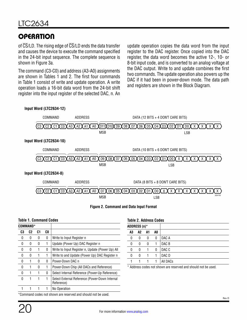
OPERATIONThe LTC2634 is a family of quad voltage output DACs in 16-lead QFN and 10-lead MSOP packages. Each DAC can operate rail-to-rail using an external reference, or with its full-scale voltage set by an integrated reference. Eighteen combinations of accuracy (12-, 10- and 8-bit), power-on reset value (zero-scale, mid-scale in internal reference mode, or mid-scale in external reference mode), and full-scale voltage (2.5V or 4.096V) are available. The LTC2634 is controlled using a 3-wire SPI/MICROWIRE compatible interface.
Power-On Reset
The LTC2634-HZ/LTC2634-LZ clear the output to zero-scale when power is first applied, making system initial-ization consistent and repeatable.
For some applications, downstream circuits are active during DAC power-up, and may be sensitive to nonzero outputs from the DAC during this time. The LTC2634 contains circuitry to reduce the power-on glitch: the analog output typically rises less than 5mV above zero-scale during power on. In general, the glitch amplitude decreases as the power supply ramp time is increased. See “Power-On Reset Glitch” in the Typical Performance Characteristics section.
The LTC2634-HMI/LTC2634-HMX/LTC2634-LMI/LTC2634-LMX provide an alternative reset, setting the output to mid-scale when power is first applied. The LTC2634-LMI and LTC2634-HMI power up in internal reference mode, with the output set to a mid-scale volt-age of 1.25V and 2.048V, respectively. The LTC2634-LMX and LTC2634-HMX power up in external reference mode, with the output set to mid-scale of the external reference. Default reference mode selection is described in the Reference Modes section.
Power Supply Sequencing
The voltage at REF (Pin 10, QFN/Pin 7, MSOP) must be kept within the range –0.3V ≤ VREF ≤ VCC + 0.3V (see Absolute Maximum Ratings). Particular care should be taken to observe these limits during power supply turn-on and turn-off sequences, when the voltage at VCC is in transition.
Transfer Function
The digital-to-analog transfer function is:
VOUT(IDEAL) =
k
2N
VREF – VREFLO( )+ VREFLO
where k is the decimal equivalent of the binary DAC input code, N is the resolution, and VREF is either 2.5V (LTC2634-LMI/LTC2634-LMX/LTC2634-LZ) or 4.096V (LTC2634-HMI/LTC2634-HMX/LTC2634-HZ) when in internal reference mode, and the voltage at REF when in external reference mode. The resulting DAC output span is 0V to VREF , as it is necessary to tie REFLO to GND.
Serial Interface
The CS/LD input is level-triggered. When this input is taken low, it acts as a chip-select signal, enabling the SDI and SCK buffers and the input shift register. Data (SDI input) is transferred at the next 24 rising SCK edges. The 4-bit command, C3-C0, is loaded first; then the 4-bit DAC address, A3-A0; and finally the 16-bit data word. The data word comprises the 12-, 10- or 8-bit input code, ordered MSB to LSB, followed by 4, 6 or 8 don’t-care bits (LTC2634-12/LTC2634-10/LTC2634-8 respectively; see Figure 2). Data can only be transferred to the device when the CS/LD signal is low, beginning on the first rising edge of SCK. SCK may be high or low at the falling edge
LTC2634
20Rev D
For more information www.analog.com
OPERATION
C3
COMMAND
Input Word (LTC2634-12)
ADDRESS DATA (12 BITS + 4 DON’T CARE BITS)
C2 C1 C0 A3 A2 A1 A0 D9D10D11 D8 D7 D6 D5 D4 D3 D2 D1 D0 X X X X
MSB LSB
C3
COMMAND
Input Word (LTC2634-10)
ADDRESS DATA (10 BITS + 6 DON’T CARE BITS)
C2 C1 C0 A3 A2 A1 A0 D7D8D9 D6 D5 D4 D3 D2 D1 D0 X X X X X X
MSB LSB
C3
COMMAND
Input Word (LTC2634-8)
ADDRESS DATA (8 BITS + 8 DON’T CARE BITS)
C2 C1 C0 A3 A2 A1 A0 D5D6D7 D4 D3 D2 D1 D0 X X X X X X X X
MSB LSB2634 F02
Table 1. Command CodesCOMMAND*
C3 C2 C1 C0
0 0 0 0 Write to Input Register n
0 0 0 1 Update (Power Up) DAC Register n
0 0 1 0 Write to Input Register n, Update (Power Up) All
0 0 1 1 Write to and Update (Power Up) DAC Register n
0 1 0 0 Power-Down DAC n
0 1 0 1 Power-Down Chip (All DACs and Reference)
0 1 1 0 Select Internal Reference (Power-Up Reference)
0 1 1 1 Select External Reference (Power-Down Internal Reference)
1 1 1 1 No Operation
*Command codes not shown are reserved and should not be used.
Table 2. Address CodesADDRESS (n)*
A3 A2 A1 A0
0 0 0 0 DAC A
0 0 0 1 DAC B
0 0 1 0 DAC C
0 0 1 1 DAC D
1 1 1 1 All DACs* Address codes not shown are reserved and should not be used.
Figure 2. Command and Data Input Format
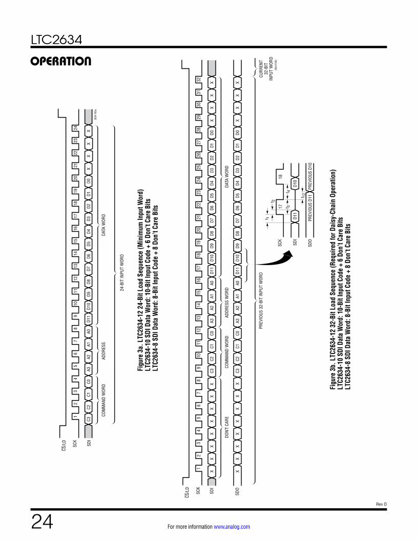
of CS/LD. The rising edge of CS/LD ends the data transfer and causes the device to execute the command specified in the 24-bit input sequence. The complete sequence is shown in Figure 3a.
The command (C3-C0) and address (A3-A0) assignments are shown in Tables 1 and 2. The first four commands in Table 1 consist of write and update operation. A write operation loads a 16-bit data word from the 24-bit shift register into the input register of the selected DAC, n. An
update operation copies the data word from the input register to the DAC register. Once copied into the DAC register, the data word becomes the active 12-, 10- or 8-bit input code, and is converted to an analog voltage at the DAC output. Write to and update combines the first two commands. The update operation also powers up the DAC if it had been in power-down mode. The data path and registers are shown in the Block Diagram.
LTC2634
21Rev D
For more information www.analog.com
OPERATIONWhile the minimum input sequence is 24 bits, it may optionally be extended to 32 bits to accommodate micro-processors that have a minimum word width of 16 bits (2 bytes). To use the 32-bit width, 8 don’t care bits must be transferred to the device first, followed by the 24-bit sequence described. Figure 3b shows the 32-bit sequence.
The 16-bit data word is ignored for all commands that do not include a write operation.
Daisy-Chain Operation (QFN Package)
The serial output of the shift register appears at the SDO pin on the QFN package. Data transferred to the device from the SDI input is delayed 32 SCK rising edges before being output at the next SCK falling edge, therefore, daisy chaining multiple LTC2634 DACs requires 32-bit data write cycles.
The SDO output can be used to facilitate control of multiple serial devices from a single 3-wire serial port (i.e., SCK, SDI and CS/LD). Such a “daisy-chain” series is config-ured by connecting SDO of each upstream device to SDI of the next device in the chain. The shift registers of the devices are thus connected in series, effectively forming a single input shift register which extends through the entire chain. Because of this, the devices can be addressed and controlled individually by simply concatenating their input words; the first instruction addresses the last device in the chain and so forth. The SCK and CS/LD signals are common to all devices in the series. Figure 5 shows a block diagram for daisy-chain operation.
In use, CS/LD is first taken low. Then the concatenated input data is transferred to the chain, using SDI of the first device as the data input. When the data transfer is complete, CS/LD is taken high, completing the instruction sequence for all devices simultaneously. A single device can be controlled by using the no-operation command (1111) for the other devices in the chain.
Reference Modes
For applications where an accurate external reference is either not available, or not desirable due to limited space, the LTC2634 has a low noise, user-selectable, integrated reference. The integrated reference voltage is internally amplified by 2x to provide the full-scale DAC output volt-age range. The LTC2634-LMI/LTC2634-LMX/LTC2634-LZ provides a full-scale DAC output of 2.5V. The LTC2634-HMI/LTC2634-HMX/LTC2634-HZ provides a full-scale DAC output of 4.096V. The internal reference can be useful in applications where the supply voltage is poorly regulated. Internal Reference mode can be selected by using command 0110b, and is the power-on default for LTC2634-HZ/LTC2634-LZ, as well as for LTC2634-HMI/LTC2634-LMI.
The 10ppm/°C, 1.25V (LTC2634-LMI/LTC2634-LMX/LTC2634-LZ) or 2.048V (LTC2634-HMI/LTC2634-HMX/LTC2634-HZ) internal reference is available at the REF pin. Adding bypass capacitance to the REF pin will improve noise performance; 0.1µF is recommended, and up to 10µF can be driven without oscillation. The REF out-put must be buffered when driving an external DC load current.
Alternatively, the DAC can operate in external reference mode using command 0111b. In this mode, an input voltage supplied externally to the REF pin provides the reference (1V ≤ VREF ≤ VCC) and the supply current is reduced. The external reference voltage supplied sets the full-scale DAC output voltage. External reference mode is the power-on default for LTC2634-HMX/LTC2634-LMX.
The reference mode of LTC2634-HZ/LTC2634-LZ/ LTC2634-HMI/LTC2634-LMI (internal reference power-on default), can be changed by software command after power up. The same is true for LTC2634-HMX/-LMX (external reference power-on default).
The LTC2634’s QFN package offers a REFLO pin for the negative reference. REFLO must be connected to GND.
LTC2634
22Rev D
For more information www.analog.com
OPERATIONPower-Down Mode
For power-constrained applications, power-down mode can be used to reduce the supply current whenever less than four DAC outputs are needed. When in power down, the buffer amplifiers, bias circuits, and integrated reference circuits are disabled, and draw essentially zero current. The DAC outputs are put into a high impedance state, and the output pins are passively pulled to ground through individual 200k resistors. Input- and DAC-register contents are not disturbed during power down.
Any DAC channel or combination of channels can be put into power-down mode by using command 0100b in com-bination with the appropriate DAC address, (n). The sup-ply current is reduced approximately 20% for each DAC powered down. The integrated reference is automatically powered down when external reference is selected using command 0111b. In addition, all the DAC channels and the integrated reference together can be put into power-down mode using power-down chip command 0101b. When the integrated reference and all DAC channels are in power-down mode, the REF pin becomes high imped-ance (typically > 1GΩ). For all power-down commands the 16-bit data word is ignored.
Normal operation resumes after executing any command that includes a DAC update, (as shown in Table 1) or pull-ing the asynchronous LDAC pin low. The selected DAC is powered up as its voltage output is updated. When a DAC which is in a powered-down state is powered up and updated, normal settling is delayed. If less than four DACs are in a powered-down state prior to the update com-mand, the power-up delay time is 10µs. However, if all four DACs and the integrated reference are powered down, then the main bias generation circuit block has been auto-matically shut down in addition to the DAC amplifiers and reference buffers. In this case, the power-up delay time is
12µs. The power-up of the integrated reference depends on the command that powered it down. If the reference is powered down using the select external reference com-mand (0111b), then it can only be powered back up using select internal reference command (0110b). However, if the reference was powered down using power-down chip command (0101b), then in addition to select internal ref-erence command (0110b), any command (in software or using the LDAC pin) that powers up the DACs will also power up the integrated reference.
Voltage Output
The LTC2634’s integrated rail-to-rail amplifier has guar-anteed load regulation when sourcing or sinking up to 10mA at 5V, and 5mA at 3V.
Load regulation is a measure of the amplifier’s ability to maintain the rated voltage accuracy over a wide range of load current. The measured change in output voltage per change in forced load current is expressed in LSB/mA.
DC output impedance is equivalent to load regulation, and may be derived from it by simply calculating a change in units from LSB/mA to ohms. The amplifier’s DC output impedance is 0.1Ω when driving a load well away from the rails.
When drawing a load current from either rail, the output voltage headroom with respect to that rail is limited by the 50Ω typical channel resistance of the output devices (e.g., when sinking 1mA, the minimum output voltage is 50Ω • 1mA, or 50mV). See the graph “Headroom at Rails vs Output Current” in the Typical Performance Characteristics section.
The amplifier is stable driving capacitive loads of up to 500pF.
LTC2634
23Rev D
For more information www.analog.com
OPERATIONRail-to-Rail Output Considerations
In any rail-to-rail voltage output device, the output is lim-ited to voltages within the supply range.
Since the analog output of the DAC cannot go below ground, it may limit for the lowest codes as shown in Figure 4b. Similarly, limiting can occur near full-scale when the REF pin is tied to VCC. If VREF = VCC and the DAC full-scale error (FSE) is positive, the output for the highest codes limits at VCC, as shown in Figure 4c. No full-scale limiting can occur if VREF is less than VCC – FSE.
Offset and linearity are defined and tested over the region of the DAC transfer function where no output limiting can occur.
Board Layout
The PC board should have separate areas for the analog and digital sections of the circuit. A single, solid ground plane should be used, with analog and digital signals care-fully routed over separate areas of the plane. This keeps digital signals away from sensitive analog signals and minimizes the interaction between digital ground currents and the analog section of the ground plane. The resistance
from the LTC2634 GND pin to the ground plane should be as low as possible. Resistance here will add directly to the effective DC output impedance of the device (typically 0.1Ω). Note that the LTC2634 is no more susceptible to this effect than any other parts of this type; on the con-trary, it allows layout-based performance improvements to shine rather than limiting attainable performance with excessive internal resistance.
Another technique for minimizing errors is to use a sepa-rate power ground return trace on another board layer. The trace should run between the point where the power supply is connected to the board and the DAC ground pin. Thus the DAC ground pin becomes the common point for analog ground, digital ground, and power ground. When the LTC2634 is sinking large currents, this current flows out the ground pin and directly to the power ground trace without affecting the analog ground plane voltage.
It is sometimes necessary to interrupt the ground plane to confine digital ground currents to the digital portion of the plane. When doing this, make the gap in the plane only as long as it needs to be to serve its purpose and ensure that no traces cross over the gap.
LTC2634
24Rev D
For more information www.analog.com
OPERATION1
23
45
67
89
1011
1213
1415
1617
1819
2021
2223
24
C2C1
C0A3
A2A1
A0D1
1D1
0D9
D8D7
D6D5
D4D3
D2D1
D0X
XX
XC3
CS/L
D
SCK
SDI
COM
MAN
D W
ORD
ADDR
ESS
DATA
WOR
D
24-B
IT IN
PUT
WOR
D
2634
F03
a
Figu
re 3
a. L
TC26
34-1
2 24
-Bit
Load
Seq
uenc
e (M
inim
um In
put W
ord)
LT
C263
4-10
SDI
Dat
a W
ord:
10-
Bit I
nput
Cod
e +
6 Do
n’t C
are
Bits
LT
C263
4-8
SDI D
ata
Wor
d: 8
-Bit
Inpu
t Cod
e +
8 Do
n’t C
are
Bits
Figu
re 3
b. L
TC26
34-1
2 32
-Bit
Load
Seq
uenc
e (R
equi
red
for D
aisy
-Cha
in O
pera
tion)
LT
C263
4-10
SDI
Dat
a W
ord:
10-
Bit I
nput
Cod
e +
6 Do
n’t C
are
Bits
LT
C263
4-8
SDI D
ata
Wor
d: 8
-Bit
Inpu
t Cod
e +
8 Do
n’t C
are
Bits
12
34
56
78
910
1112
1314
1516
1718
1920
2122
2324
2526
2728
2930
3132
C2C1
C0A3
A2A1
A0D1
1D1
0D9
D8D7
D6D5
D4D3
D2D1
D0X
XX
XC3
XX
XX
XX
XX
CS/L
D
SCK
SDI
COM
MAN
D W
ORD
ADDR
ESS
WOR
DDA
TA W
ORD
DON’
T CA
RE
C2C1
C0A3
A2A1
A0D1
1D1
0D9
D8D7
D6D5
D4D3
D2D1
D0X
XX
XC3
XX
XX
XX
XX
SDO
CURR
ENT
32-B
ITIN
PUT
WOR
D26
34 F
03b
PREV
IOUS
32-
BIT
INPU
T W
ORD
t 2
t 3t 4
t 1
t 12
D11
17SC
K
SDI
SDO
PREV
IOUS
D10
PREV
IOUS
D11
18
D10

LTC2634
25Rev D
For more information www.analog.com
OPERATION
2634 F04
INPUT CODE
(4b)
(4a)
(4c)OUTPUTVOLTAGE
NEGATIVEOFFSET
0V
2,04800V
4,095INPUT CODE
OUTPUTVOLTAGE
VREF = VCC
VREF = VCC
INPUT CODE
OUTPUTVOLTAGE
POSITIVEFSE
Figure 4. Effects of Rail-to-Rail Operation on a DAC Transfer Curve (Shown in 12 Bits) (4a) Overall Transfer Function (4b) Effect of Negative Offset for Codes Near Zero (4c) Effect of Postitive Full-Scale Error for Codes Near Full-Scale
SDI SDO
LTC2634UDSCK56 7 6 7 6 7
DATA OUTPUT
4CS/LD
SDI SDOSCK
54
CS/LD
SDI SDO
2634 F05
SCK54
CS/LD
CS/LD
SCK
SDI
LTC2634UD LTC2634UD
• • •
Figure 5. Daisy-Chain Operation (QFN Only)

LTC2634
26Rev D
For more information www.analog.com
TYPICAL APPLICATION
– +
DAC
A
DAC
D
LTC2
755
R CO
M1
R IN
160
0.1µ
F
0.1µ
F0.
1µF
2 3 4 5 6
OUTA
2 3
591
48
2 58 19
5 6
7
4 –15V
15V
8R O
FSA
R FBA
R VO
SA
GND
I OUT
1A
I OUT
2A
V DD
155V
610.
1µF
0.1µ
F
OUTC
–15V
30k
LT16
34-1
.25
OUTB
0.1µ
F
64 63 62R E
FA
–+
1/2
LT14
691/
2 LT
1469
–+ LTC6
240
15V
–15V
DAC
C
+–
+–
DAC
B
–15V
30k
–15V
30k
SERI
ALBU
S
DAC
A
DAC
B
CS/L
D
SCK
10
2634
TA0
2
89
0.1µ
F
1
GND
7RE
FLT
C263
4MSE
-LM
I12
V CC
SDI
DAC
C
DAC
D
M9
M3
M1
OUT
V OUT
±5V
LT19
91RE
FV E
E
V CC
8 9 10
P1 P3 P9
1 2 3
5V0.
1µF
0.1µ
F
47
5
6
15V
–15V
LT16
34-1
.25
LT16
34-1
.25
LTC2
634
DACs
Adj
usts
LTC
2755
-16
Offs
ets,
Am
plifi
ed w
ith LT
®19
91 P
GA to
±5V

LTC2634
27Rev D
For more information www.analog.com
PACKAGE DESCRIPTIONPlease refer to http://www.linear.com/product/LTC2634#packaging for the most recent package drawings.
3.00 ±0.10(4 SIDES)
RECOMMENDED SOLDER PAD PITCH AND DIMENSIONS
1.45 ±0.05(4 SIDES)
NOTE:1. DRAWING CONFORMS TO JEDEC PACKAGE OUTLINE MO-220 VARIATION (WEED-2)2. DRAWING NOT TO SCALE3. ALL DIMENSIONS ARE IN MILLIMETERS4. DIMENSIONS OF EXPOSED PAD ON BOTTOM OF PACKAGE DO NOT INCLUDE MOLD FLASH. MOLD FLASH, IF PRESENT, SHALL NOT EXCEED 0.15mm ON ANY SIDE5. EXPOSED PAD SHALL BE SOLDER PLATED6. SHADED AREA IS ONLY A REFERENCE FOR PIN 1 LOCATION ON THE TOP AND BOTTOM OF PACKAGE
PIN 1TOP MARK(NOTE 6)
0.40 ±0.10
BOTTOM VIEW—EXPOSED PAD
1.45 ± 0.10(4-SIDES)
0.75 ±0.05 R = 0.115TYP
0.25 ±0.05
1
PIN 1 NOTCH R = 0.20 TYPOR 0.25 × 45° CHAMFER
15 16
2
0.50 BSC
0.200 REF
2.10 ±0.053.50 ±0.05
0.70 ±0.05
0.00 – 0.05
(UD16) QFN 0904
0.25 ±0.050.50 BSC
PACKAGE OUTLINE
UD Package16-Lead Plastic QFN (3mm × 3mm)
(Reference LTC DWG # 05-08-1691 Rev Ø)

LTC2634
28Rev D
For more information www.analog.com
PACKAGE DESCRIPTIONPlease refer to http://www.linear.com/product/LTC2634#packaging for the most recent package drawings.
MSOP (MSE) 0213 REV I
0.53 ±0.152(.021 ±.006)
SEATINGPLANE
0.18(.007)
1.10(.043)MAX
0.17 – 0.27(.007 – .011)
TYP
0.86(.034)REF
0.50(.0197)
BSC
1 2 3 4 5
4.90 ±0.152(.193 ±.006)
0.497 ±0.076(.0196 ±.003)
REF8910
10
1
7 6
3.00 ±0.102(.118 ±.004)
(NOTE 3)
3.00 ±0.102(.118 ±.004)
(NOTE 4)
NOTE:1. DIMENSIONS IN MILLIMETER/(INCH)2. DRAWING NOT TO SCALE3. DIMENSION DOES NOT INCLUDE MOLD FLASH, PROTRUSIONS OR GATE BURRS. MOLD FLASH, PROTRUSIONS OR GATE BURRS SHALL NOT EXCEED 0.152mm (.006") PER SIDE4. DIMENSION DOES NOT INCLUDE INTERLEAD FLASH OR PROTRUSIONS. INTERLEAD FLASH OR PROTRUSIONS SHALL NOT EXCEED 0.152mm (.006") PER SIDE5. LEAD COPLANARITY (BOTTOM OF LEADS AFTER FORMING) SHALL BE 0.102mm (.004") MAX6. EXPOSED PAD DIMENSION DOES INCLUDE MOLD FLASH. MOLD FLASH ON E-PAD SHALL NOT EXCEED 0.254mm (.010") PER SIDE.
0.254(.010) 0° – 6° TYP
DETAIL “A”
DETAIL “A”
GAUGE PLANE
5.10(.201)MIN
3.20 – 3.45(.126 – .136)
0.889 ±0.127(.035 ±.005)
RECOMMENDED SOLDER PAD LAYOUT
1.68 ±0.102(.066 ±.004)
1.88 ±0.102(.074 ±.004)
0.50(.0197)
BSC0.305 ± 0.038(.0120 ±.0015)
TYP
BOTTOM VIEW OFEXPOSED PAD OPTION
1.68(.066)
1.88(.074)
0.1016 ±0.0508(.004 ±.002)
DETAIL “B”
DETAIL “B”CORNER TAIL IS PART OF
THE LEADFRAME FEATURE.FOR REFERENCE ONLY
NO MEASUREMENT PURPOSE
0.05 REF
0.29REF
MSE Package10-Lead Plastic MSOP, Exposed Die Pad
(Reference LTC DWG # 05-08-1664 Rev I)
LTC2634
29Rev D
For more information www.analog.com
Information furnished by Analog Devices is believed to be accurate and reliable. However, no responsibility is assumed by Analog Devices for its use, nor for any infringements of patents or other rights of third parties that may result from its use. Specifications subject to change without notice. No license is granted by implication or otherwise under any patent or patent rights of Analog Devices.
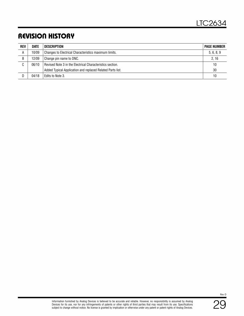
REVISION HISTORYREV DATE DESCRIPTION PAGE NUMBER
A 10/09 Changes to Electrical Characteristics maximum limits. 5, 6, 8, 9
B 12/09 Change pin name to DNC. 2, 16
C 06/10 Revised Note 3 in the Electrical Characteristics section.Added Typical Application and replaced Related Parts list.
1030
D 04/18 Edits to Note 3. 10

LTC2634
30Rev D
For more information www.analog.com ANALOG DEVICES, INC. 2009
D16828-0-4/18(D)www.analog.com
RELATED PARTS
TYPICAL APPLICATION
–
+DAC A
DAC D
LTC2755
RCOM1
RIN160 0.1µF
0.1µF 0.1µF
2
3
4
5
6
OUTA
2
3
591
4
8
2
58
19
5
6
7
4
–15V
15V
8ROFSA
RFBA
RVOSA
GND
IOUT1A
IOUT2A
VDD15
5V
610.1µF
0.1µF
OUTC
–15V
30k
LT1634-1.25
OUTB
0.1µF
64
63
62 REFA
–
+1/2 LT1469
1/2 LT1469
–
+
LTC6240
15V
–15V
DAC C+–
+–
DAC B
–15V
30k
–15V
30k SERIALBUS
DAC A
DAC B
CS/LD
SCK10
2634 TA02
8
9
0.1µF
1
GND
7REF LTC2634MSE-LMI12 VCC
SDI
DAC C
DAC D
M9M3M1
OUT VOUT±5VLT1991
REFVEE
VCC
89
10
P1P3P9
123
5V 0.1µF
0.1µF
4
7
5
6
15V
–15VLT1634-1.25
LT1634-1.25
LTC2634 DACs Adjusts LTC2755-16 Offsets, Amplified with LT1991 PGA to ±5V
PART NUMBER DESCRIPTION COMMENTS
LTC2654/LTC2655 Quad 16-/12 Bit, SPI/I2C VOUT DACs with 10ppm/°C Maximum Reference
±4LSB INL Maximum at 16 Bits and ±2mV Offset Error, Rail-to-Rail Output, 20-Lead 4mm × 4mm QFN and 16-Lead Narrow SSOP Packages
LTC2604/LTC2614/LTC2624
Quad 16-/14-/12-Bit, SPI VOUT DACs with External Reference
250µA per DAC, 2.5V to 5.5V Supply Range, Rail-to-Rail Output, 16-Lead SSOP Package
LTC2609/LTC2619/LTC2629
Quad 16-/14-/12-Bit VOUT DACs with I2C Interface 250µA per DAC, 2.7V to 5.5V Supply Range, Rail-to-Rail Output with Separate VREF Pins for Each DAC
LTC2635 Quad 12-/10-/8-Bit I2C VOUT DACs with 10ppm/°C Reference
±2.5LSB INL, 2.7V to 5.5V Supply Range, 10ppm/°C Reference, External REF Mode, 16-Pin 3mm × 3mm QFN and 10-Lead MSOP Packages
LTC2656/LTC2657 Octal 16-/12 Bit, SPI/I2C VOUT DACs with 10ppm/°C Maximum Reference
±4LSB INL Maximum at 16 Bits and ±2mV Offset Error, Rail-to-Rail Output, 20-Lead 4mm × 5mm QFN and 16-Lead TSSOP Packages
LTC2636/LTC2637 Octal 12-/10-/8-Bit, SPI/I2C VOUT DACs with 10ppm/°C Reference
125µA per DAC, 2.7V to 5.5V Supply Range, 10ppm/°C Reference, External REF Mode, Rail-to-Rail Output, 14-Lead 4mm × 3mm DFN and 16-Lead MSOP Packages
LTC2630/LTC2631 Single 12-/10-/8-Bit, SPI/ I2C VOUT DACs with 10ppm/°C Reference
180µA per DAC, 2.7V to 5.5V Supply Range, 10ppm/°C Reference, Rail-to-Rail Output, SC70 (LTC2630)/ThinSOT™ (LTC2631) Packages
LTC2640 Single 12-/10-/8-Bit, SPI VOUT DACs with 10ppm/°C Reference
180µA per DAC, 2.7V to 5.5V Supply Range, 10ppm/°C Reference, External REF Mode, Rail-to-Rail Output, ThinSOT Package
LTC1664 Quad 10-Bit, Serial VOUT DAC VCC = 2.7V to 5.5V, Micropower, Rail-to-Rail Output in 16-Pin Narrow SSOP
Amplifiers
LT1991 Precision, 100µA Gain Selectable Amplifier Gain Accuracy of 0.04%, Gains from –13 to 14, 100µA precision Op Amp
LT1469 Dual 90MHz, 22V/µs 16-Bit Accurate Operational Amplifier
90MHz Gain Bandwidth, 125µV Offset, 900ns, 22V/µs Slew Rate Precision Op Amp