LQ035NC111 V01 20070912 - file.yizimg.comfile.yizimg.com/4611/2012091312211687.pdf · Display...
28
Product Specifications Customer Description 3.45” TFT LCD Module Model Name LQ035NC111 Date 2007/9/12 Doc. No. Revision 01 Customer Approval Date The above signature represents that the product specifications, testing regulation, and warranty in the specifications are accepted Engineering Check Date Prepared Date Head Office & Factory : No. 71, Te Lun Rd., Jen Te Hsiang, Tainan County 717, Taiwan, R.O.C. TEL: +886-6-279-4113 FAX: +886-6-279-1194 CHILIN TECHNOLOGY CO., LTD.
Transcript of LQ035NC111 V01 20070912 - file.yizimg.comfile.yizimg.com/4611/2012091312211687.pdf · Display...
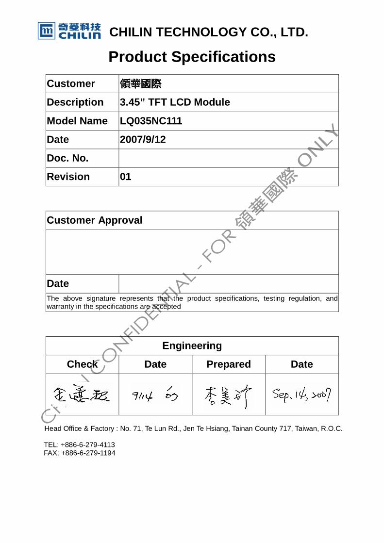
Product Specifications
Customer ����������������
Description 3.45” TFT LCD Module
Model Name LQ035NC111
Date 2007/9/12
Doc. No.
Revision 01
Customer Approval
Date
The above signature represents that the product specifications, testing regulation, and warranty in the specifications are accepted
Engineering
Check Date Prepared Date
Head Office & Factory : No. 71, Te Lun Rd., Jen Te Hsiang, Tainan County 717, Taiwan, R.O.C. TEL: +886-6-279-4113 FAX: +886-6-279-1194
CHILIN TECHNOLOGY CO., LTD.
Doc. No.
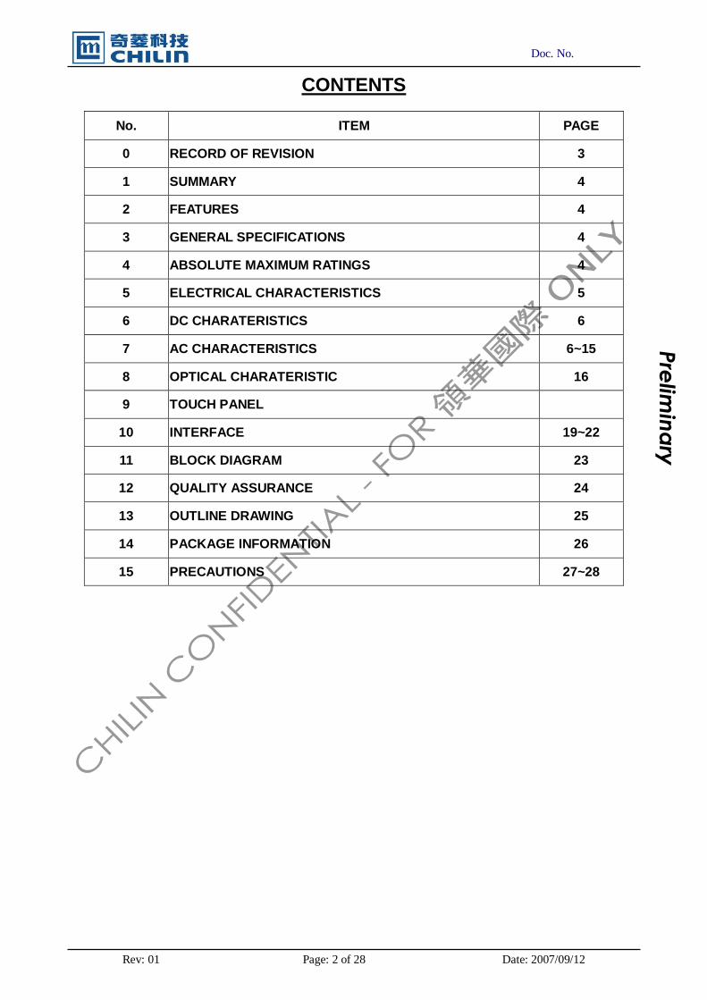
Rev: 01 Page: 2 of 28 Date: 2007/09/12
Preliminary CONTENTS
No. ITEM PAGE
0 RECORD OF REVISION 3
1 SUMMARY 4
2 FEATURES 4
3 GENERAL SPECIFICATIONS 4
4 ABSOLUTE MAXIMUM RATINGS 4
5 ELECTRICAL CHARACTERISTICS 5
6 DC CHARATERISTICS 6
7 AC CHARACTERISTICS 6~15
8 OPTICAL CHARATERISTIC 16
9 TOUCH PANEL
10 INTERFACE 19~22
11 BLOCK DIAGRAM 23
12 QUALITY ASSURANCE 24
13 OUTLINE DRAWING 25
14 PACKAGE INFORMATION 26
15 PRECAUTIONS 27~28
Doc. No.
Rev: 01 Page: 3 of 28 Date: 2007/09/12
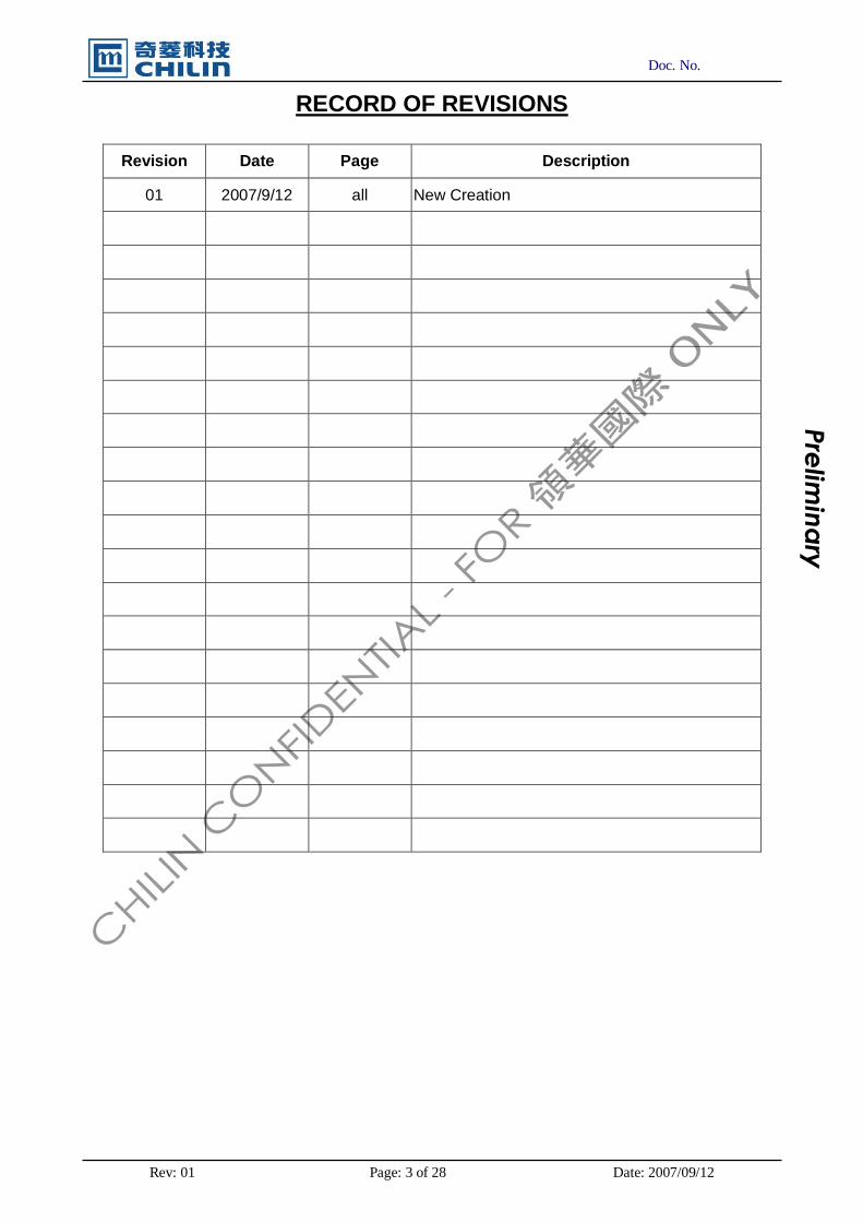
Preliminary RECORD OF REVISIONS
Revision Date Page Description
01 2007/9/12 all New Creation
Doc. No.
Rev: 01 Page: 4 of 28 Date: 2007/09/12
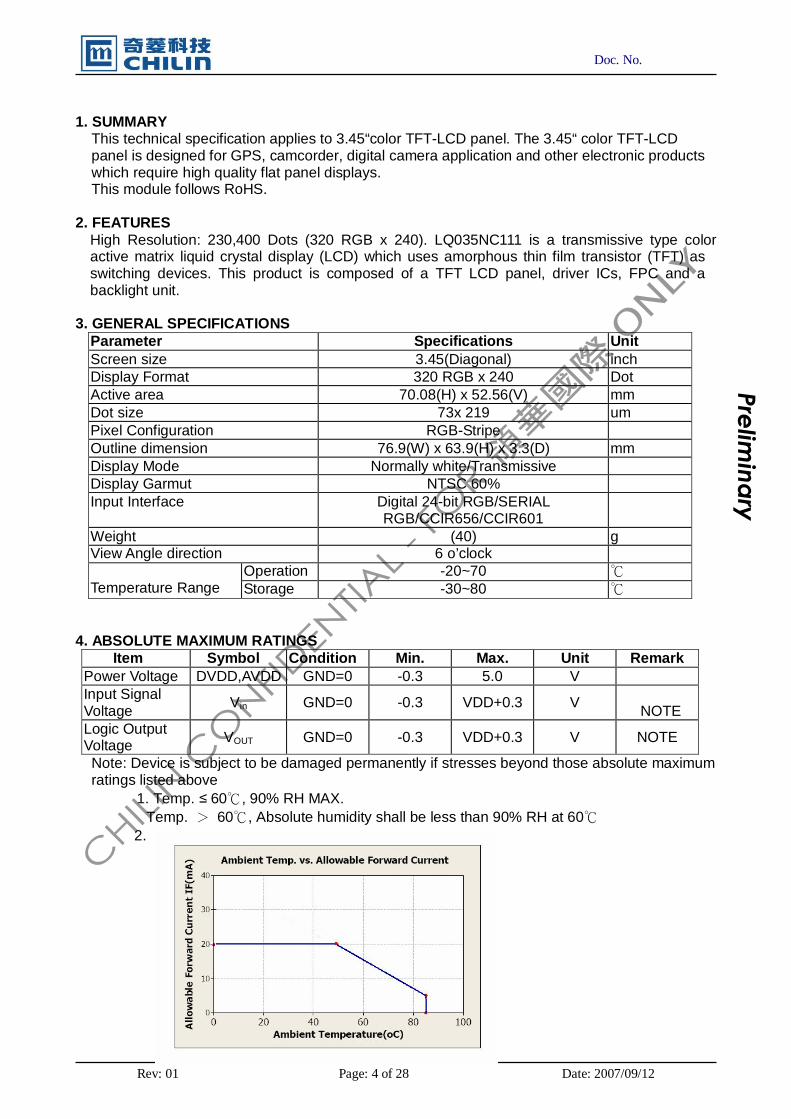
Preliminary 1. SUMMARY
This technical specification applies to 3.45“color TFT-LCD panel. The 3.45“ color TFT-LCD panel is designed for GPS, camcorder, digital camera application and other electronic products which require high quality flat panel displays. This module follows RoHS.
2. FEATURES
High Resolution: 230,400 Dots (320 RGB x 240). LQ035NC111 is a transmissive type color active matrix liquid crystal display (LCD) which uses amorphous thin film transistor (TFT) as switching devices. This product is composed of a TFT LCD panel, driver ICs, FPC and a backlight unit.
3. GENERAL SPECIFICATIONS Parameter Specifications Unit Screen size 3.45(Diagonal) inch Display Format 320 RGB x 240 Dot Active area 70.08(H) x 52.56(V) mm Dot size 73x 219 um Pixel Configuration RGB-Stripe Outline dimension 76.9(W) x 63.9(H) x 3.3(D) mm Display Mode Normally white/Transmissive Display Garmut NTSC 60% Input Interface Digital 24-bit RGB/SERIAL
RGB/CCIR656/CCIR601
Weight (40) g View Angle direction 6 o’clock
Operation -20~70 � Temperature Range Storage -30~80 �
4. ABSOLUTE MAXIMUM RATINGS
Item Symbol Condition Min. Max. Unit Remark Power Voltage DVDD,AVDD GND=0 -0.3 5.0 V Input Signal Voltage Vin GND=0 -0.3 VDD+0.3 V
NOTE Logic Output Voltage VOUT GND=0 -0.3 VDD+0.3 V NOTE
Note: Device is subject to be damaged permanently if stresses beyond those absolute maximum ratings listed above
1. Temp. ≤ 60 , 90% RH MAX. � Temp. � 60 , Absolute humidity shall be less than 90% RH at 60� � 2.

Doc. No.
Rev: 01 Page: 5 of 28 Date: 2007/09/12
Preliminary
5. ELECTRICAL CHARACTERISTICS 5.1. Operating conditions:
Rating Parameter Symbol Min. Typ. Max.
Unit Condition
Power Voltage VCC 3.0 3.3 3.6 V
Digital Operation Current Icc 8.6 mA
� Gate On Power VGH 1 4 1 5 1 8 V
Gate Of f Power VGL -1 1 -1 0 -8 V
Vc om H i g h Vol tag e Vc om H 3. 7 V Note1
Vc om l ow Vol tag e Vc om L -1 . 6 V Note1
Vc om l ev el m ax Vc om A 6 V
Note1. VcomH& VcomL�Adjust the color with gamma data. Vp-p should be higher then 4V.(Option 5V)
Note: Please power on following the sequence VCC � VDD
5.2 LED driving conditions Parameter Symbol Min. Typ. Max. Unit Remark
LED current - 20 - mA Power Consumption - 400 420 mW LED voltage VBL+ 18.6 19.8 21 V Note 1 LED Life Time - (50,000)- - Hr Note 2,3
Note 1 : There are 1 Groups LED
Note 2 : Ta = 25 � Note 3 : Brightess to be decreased to 50% of the initial value
ILED
Doc. No.
Rev: 01 Page: 6 of 28 Date: 2007/09/12
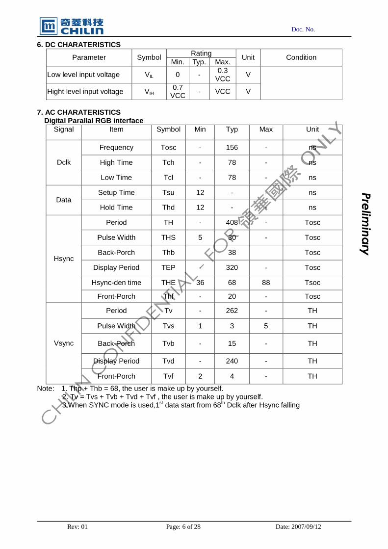
Preliminary 6. DC CHARATERISTICS
Rating Parameter Symbol Min. Typ. Max.
Unit Condition
Low level input voltage VIL 0 - 0.3 VCC V
Hight level input voltage VIH 0.7 VCC - VCC V
7. AC CHARATERISTICS Digital Parallal RGB interface
Signal Item Symbol Min Typ Max Unit
Frequency Tosc - 156 - ns
High Time Tch - 78 - ns Dclk
Low Time Tcl - 78 - ns
Setup Time Tsu 12 - - ns Data
Hold Time Thd 12 - - ns
Period TH - 408 - Tosc
Pulse Width THS 5 30 - Tosc
Back-Porch Thb 38 Tosc
Display Period TEP - 320 - Tosc
Hsync-den time THE 36 68 88 Tsoc
Hsync
Front-Porch Thf - 20 - Tosc
Period Tv - 262 - TH
Pulse Width Tvs 1 3 5 TH
Back-Porch Tvb - 15 - TH
Display Period Tvd - 240 - TH
Vsync
Front-Porch Tvf 2 4 - TH
Note: 1. Thp + Thb = 68, the user is make up by yourself. 2. Tv = Tvs + Tvb + Tvd + Tvf , the user is make up by yourself. 3.When SYNC mode is used,1st data start from 68th Dclk after Hsync falling

Doc. No.
Rev: 01 Page: 7 of 28 Date: 2007/09/12
Preliminary Digital Serial RGB interface
Signal Item Symbol Min Typ Max Unit
Frequency Tosc - 52 - ns
High Time Tch - 78 - ns Dclk
Low Time Tcl - 78 - ns
Setup Time Tsu 12 - - ns Data
Hold Time Thd 12 - - ns
Period TH - 1224 - Tosc
Pulse Width THS 5 90 - Tosc
Back-Porch Thb 114 Tosc
Display Period TEP - 960 - Tosc
Hsync-den time THE 108 204 264
Hsync
Front-Porch Thf - 60 - Tosc
Period Tv - 262 - TH
Pulse Width Tvs 1 3 5 TH
Back-Porch Tvb - 15 - TH
Display Period Tvd - 240 - TH
Vsync
Front-Porch Tvf 2 4 - TH
Note: 1. Thp + Thb = 204, the user is make up by yourself. 2. Tv = Tvs + Tvb + Tvd + Tvf , the user is make up by yourself. 3. When SYNC mode is used,1st data start from 204th Dclk after Hsync falling CCIR601/656 Interface
Signal Item Symbol Min Typ Max Unit
Frequency Tosc - 37 - ns
High Time Tch - 78 - ns Dclk
Low Time Tcl - 78 - ns
Setup Time Tsu 12 - - ns Data
Hold Time Thd 12 - - ns

Doc. No.
Rev: 01 Page: 8 of 28 Date: 2007/09/12
Preliminary 7.1 Waveform
Figure1 CLK,DATA and HIS waveforms in CCIR601
Figure2 CLK and DATA waveforms in CCIR656
Figure3 CLK, DATA and DE waveforms in Digital Serial RGB
Figure4 CLK, DATA and DE waveforms in Digital Parallel RGB

Doc. No.
Rev: 01 Page: 9 of 28 Date: 2007/09/12
Preliminary 7.1.1 Standby ON/OFF Control
LQ35HC112 has a power ON/OFF sequence control function. When STB pin is pulled L,blank data is outputted for 5-frames first, form the falling edge of the following VSYNC signal. The blank data would be gray level 255 for normally white LC.
Figure5 Standby ON/OFF Control
7.1.2 Clock and Sync waveforms
Figure6 CLK and IHS timing waveform
Figure7 IHS and IVS timing waveforms
Doc. No.
Rev: 01 Page: 10 of 28 Date: 2007/09/12
Preliminary
TVB TVS
TV
VSY N C
H SY N C
H SY N C
D C L K
D A TA Va l i d D a t a
TE P
TH
TH S TC L K
TVD
TH B TH F
TVF
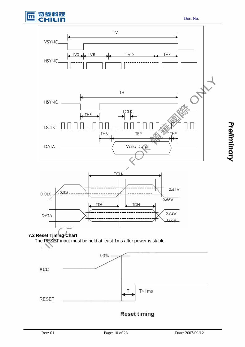
7.2 Reset Timing Chart The RESET input must be held at least 1ms after power is stable

Doc. No.
Rev: 01 Page: 11 of 28 Date: 2007/09/12
Preliminary
7.3 Digital RGB timing waveform Hsync and Vsync timing
7.3.1 Hsync and horizontal control timing waveform
7.3.2 Hsync and vertical shift clock timing waveform
Doc. No.
Rev: 01 Page: 12 of 28 Date: 2007/09/12
Preliminary
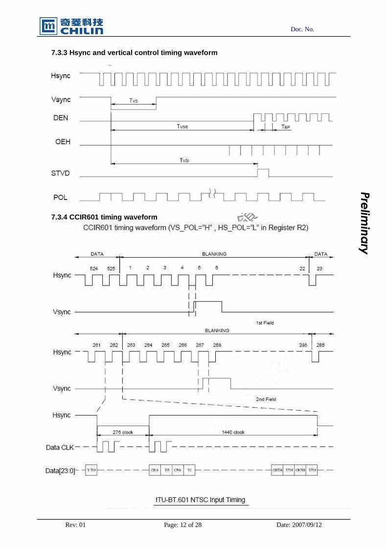
7.3.3 Hsync and vertical control timing waveform
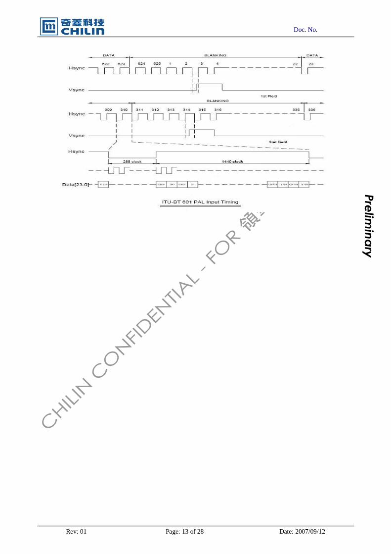
7.3.4 CCIR601 timing waveform
Doc. No.
Rev: 01 Page: 13 of 28 Date: 2007/09/12
Preliminary

Doc. No.
Rev: 01 Page: 14 of 28 Date: 2007/09/12
Preliminary 7.3.5 Source Driver Timing Chart
Doc. No.
Rev: 01 Page: 15 of 28 Date: 2007/09/12
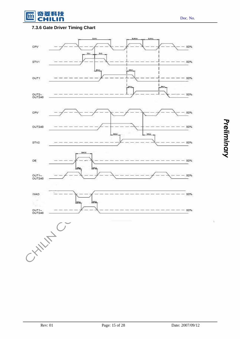
Preliminary 7.3.6 Gate Driver Timing Chart
Doc. No.
Rev: 01 Page: 16 of 28 Date: 2007/09/12
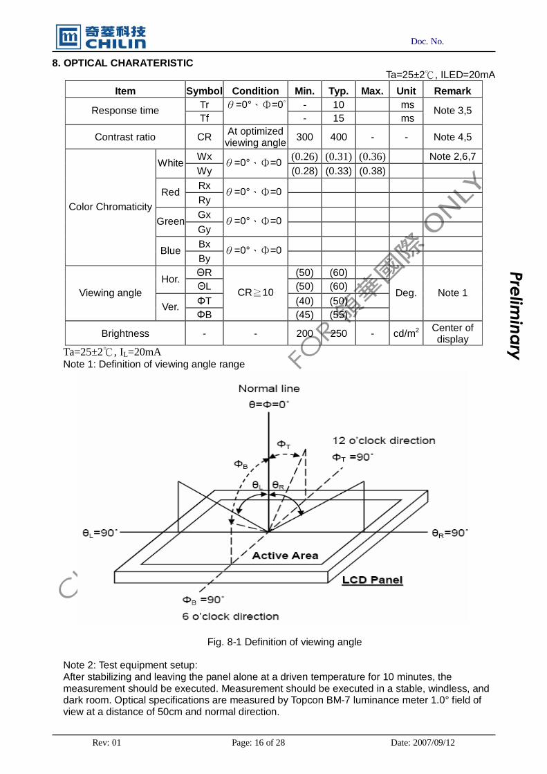
Preliminary 8. OPTICAL CHARATERISTIC
Ta=25±2 , ILED=20mA�
Item Symbol Condition Min. Typ. Max. Unit Remark Tr - 10 .ms Response time Tf
�=0°��=0� - 15 .ms
Note 3,5
Contrast ratio CR At optimized viewing angle 300 400 - - Note 4,5
Wx (0.26) (0.31) (0.36) Note 2,6,7 White
Wy �=0°��=0
(0.28) (0.33) (0.38) Rx
Red Ry
�=0°��=0
Gx Green
Gy �=0°��=0
Bx
Color Chromaticity
Blue By
�=0°��=0
ΘR (50) (60) Hor. ΘL (50) (60)
ΦT (40) (50) Viewing angle
Ver. ΦB
CR�10
(45) (55)
Deg. Note 1
Brightness - - 200 250 - cd/m2 Center of display
Ta=25±2�, IL=20mA Note 1: Definition of viewing angle range
Fig. 8-1 Definition of viewing angle
Note 2: Test equipment setup: After stabilizing and leaving the panel alone at a driven temperature for 10 minutes, the measurement should be executed. Measurement should be executed in a stable, windless, and dark room. Optical specifications are measured by Topcon BM-7 luminance meter 1.0° field of view at a distance of 50cm and normal direction.
Doc. No.
Rev: 01 Page: 17 of 28 Date: 2007/09/12
Preliminary
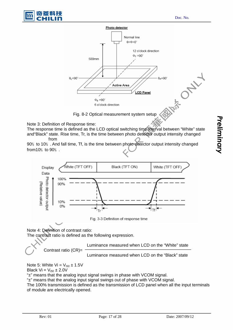
Fig. 8-2 Optical measurement system setup
Note 3: Definition of Response time: The response time is defined as the LCD optical switching time interval between “White” state and“Black” state. Rise time, Tr, is the time between photo detector output intensity changed
from 90to 10. And fall time, Tf, is the time between photo detector output intensity changed from10to 90.
Note 4: Definition of contrast ratio: The contrast ratio is defined as the following expression.
Luminance measured when LCD on the “White” state
Contrast ratio (CR)= Luminance measured when LCD on the “Black” state
Note 5: White Vi = Vi50 ± 1.5V Black Vi = Vi50 ± 2.0V “±” means that the analog input signal swings in phase with VCOM signal. “±” means that the analog input signal swings out of phase with VCOM signal. The 100% transmission is defined as the transmission of LCD panel when all the input terminals of module are electrically opened.
Doc. No.
Rev: 01 Page: 18 of 28 Date: 2007/09/12
Preliminary
Note 6: Definition of color chromaticity (CIE 1931) Color coordinates measured at the center point of LCD
Note 7: Measured at the center area of the panel when all the input terminals of LCD panel are electrically opened.
Brightness (min) Note 8 : Uniformity (U) = x 100%
Brightness (max)
Doc. No.
Rev: 01 Page: 19 of 28 Date: 2007/09/12
Preliminary 10. INTERFACE
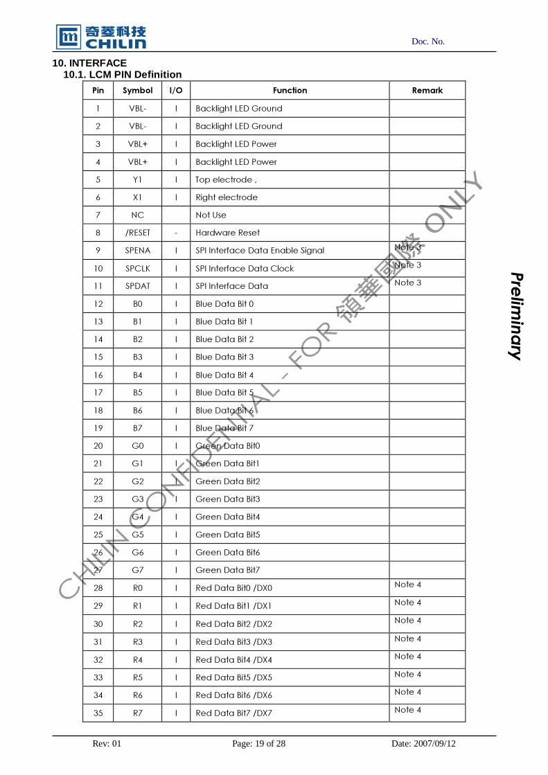
10.1. LCM PIN Definition Pin S y m b o l I / O F u nc t io n R e m a r k 1 VB L - I B ac k l i g h t L E D G r o u n d
2 VB L - I B ac k l i g h t L E D G r o u n d
3 VB L + I B ac k l i g h t L E D P o w e r
4 VB L + I B ac k l i g h t L E D P o w e r
5 Y1 I T o p e l e c t r o d e ,
6 X1 I R i g h t e l e c t r o d e
7 N C N o t U s e
8 / R E S E T - H ar d w ar e R e s e t
9 S P E N A I S P I In t e r f ac e D at a E n ab l e S i g n al N o t e 3
10 S P C L K I S P I In t e r f ac e D at a C l o c k N o t e 3
11 S P D A T I S P I In t e r f ac e D at a N o t e 3
12 B 0 I B l u e D at a B i t 0
13 B 1 I B l u e D at a B i t 1
14 B 2 I B l u e D at a B i t 2
15 B 3 I B l u e D at a B i t 3
16 B 4 I B l u e D at a B i t 4
17 B 5 I B l u e D at a B i t 5
18 B 6 I B l u e D at a B i t 6
19 B 7 I B l u e D at a B i t 7
20 G 0 I G r e e n D at a B i t 0
21 G 1 I G r e e n D at a B i t 1
22 G 2 I G r e e n D at a B i t 2
23 G 3 I G r e e n D at a B i t 3
24 G 4 I G r e e n D at a B i t 4
25 G 5 I G r e e n D at a B i t 5
26 G 6 I G r e e n D at a B i t 6
27 G 7 I G r e e n D at a B i t 7
28 R 0 I R e d D at a B i t 0 / D X0 N o t e 4
29 R 1 I R e d D at a B i t 1 / D X1 N o t e 4
30 R 2 I R e d D at a B i t 2 / D X2 N o t e 4
31 R 3 I R e d D at a B i t 3 / D X3 N o t e 4
32 R 4 I R e d D at a B i t 4 / D X4 N o t e 4
33 R 5 I R e d D at a B i t 5 / D X5 N o t e 4
34 R 6 I R e d D at a B i t 6 / D X6 N o t e 4
35 R 7 I R e d D at a B i t 7 / D X7 N o t e 4

Doc. No.
Rev: 01 Page: 20 of 28 Date: 2007/09/12
Preliminary 36 H S YN C I H o r i z o n t al S y n c In p u t
37 VS YN C I Ve r t i c al S y n c In p u t
38 D C L K I D o t D at a C l o c k
39 N C N o t U s e
40 N C N o t U s e
41 VCC I D i g i t al P o w e r
42 VCC I D i g i t al P o w e r
43 Y2 I B o t t o m e l e c t r o d e
44 X2 I L e f t e l e c t r o d e
45 N C N o t U s e
46 N C - N o t U s e
47 N C N o t U s e
48 IF 2 I C o n t r o l t h e i n p u t d at a f o r m at / f l o at i n g N o t e 1
49 IF 1 I C o n t r o l t h e i n p u t d at a f o r m at N o t e 1,5
5 0 IF 0 I C o n t r o l t h e i n p u t d at a f o r m at N o t e 1,5
5 1 N C N o t U s e
5 2 D E I D at a E n ab l e In p u t N o t e 2
5 3 G N D I G r o u n d
5 4 G N D I G r o u n d
Note: 1. The mode control (IF2) not use ,it can’t control CCIR601 interface , If not use CCIR601 ,it
can floating. 2. For digital RGB input data format, both SYNC mode and DE+SYNC mode are supported. If DE
signal is fixed low, SYNC mode is used. Otherwise, DE+SYNC mode is used.Suggest used SYNC mode!! 3. usually pull high. 4. IF select serial RGB or CCIR601/656 input mode is selected,only DX0-DX7 used,and the other short to GND, Only
selected serial RGB�CCIR601/656 interface,DX BUS will enable,Digital input mode DX0 is LSB and DX7 is MSB.
5. C o n t r o l t h e i n p u t d at a f o r m at
Doc. No.
Rev: 01 Page: 21 of 28 Date: 2007/09/12
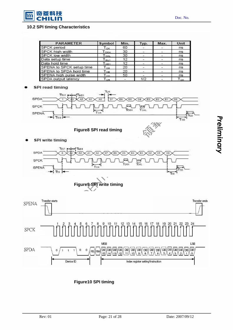
Preliminary 10.2 SPI timing Characteristics
Figure8 SPI read timing
Figure9 SPI write timing
Figure10 SPI timing
Doc. No.
Rev: 01 Page: 22 of 28 Date: 2007/09/12
Preliminary
10.3 SPI Register Description
Will be showing on Application Note From Chilintech.
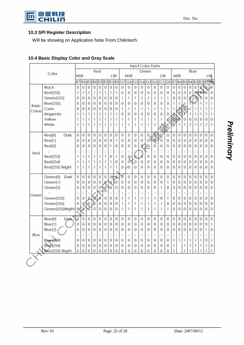
10.4 Basic Display Color and Gray Scale
In p u t C o l o r D at a R e d
M S B L S B G r e e n
M S B L S B B l u e
M S B L S B C o l o r R 7 R 6 R 5 R 4 R 3 R 2 R 1 R 0 G 7 G 6 G 5 G 4 G 3 G 2 G 1 G 0 B 7 B 6 B 5 B 4 B 3 B 2 B 1 B 0
B as i c C o l o r s
B l ac k R e d ( 25 5 ) G r e e n ( 25 5 ) B l u e ( 25 5 ) C y an M ag e n t a Ye l l o w W h i t e
0 1 0 0 0 1 1 1
0 1 0 0 0 1 1 1
0 1 0 0 0 1 1 1
0 1 0 0 0 1 1 1
0 1 0 0 0 1 1 1
0 1 0 0 0 1 1 1
0 1 0 0 0 1 1 1
0 1 0 0 0 1 1 1
0 0 1 0 1 0 1 1
0 0 1 0 1 0 1 1
0 0 1 0 1 0 1 1
0 0 1 0 1 0 1 1
0 0 1 0 1 0 1 1
0 0 1 0 1 0 1 1
0 0 1 0 1 0 1 1
0 0 1 0 1 0 1 1
0 0 0 1 1 1 0 1
0 0 0 1 1 1 0 1
0 0 0 1 1 1 0 1
0 0 0 1 1 1 0 1
0 0 0 1 1 1 0 1
0 0 0 1 1 1 0 1
0 0 0 1 1 1 0 1
0 0 0 1 1 1 0 1
R e d
R e d ( 0) D ar k R e d ( 1) R e d ( 2) :
R e d ( 25 3) R e d ( 25 4) R e d ( 25 5 ) B r i g h t
0 0 0 : 1 1 1
0 0 0 : 1 1 1
0 0 0 : 1 1 1
0 0 0 : 1 1 1
0 0 0 : 1 1 1
0 0 0 : 1 1 1
0 0 1 : 0 1 1
0 1 0 : 1 0 1
0 0 0 : 0 0 0
0 0 0 : 0 0 0
0 0 0 : 0 0 0
0 0 0 : 0 0 0
0 0 0 : 0 0 0
0 0 0 : 0 0 0
0 0 0 : 0 0 0
0 0 0 : 0 0 0
0 0 0 : 0 0 0
0 0 0 : 0 0 0
0 0 0 : 0 0 0
0 0 0 : 0 0 0
0 0 0 : 0 0 0
0 0 0 : 0 0 0
0 0 0 : 0 0 0
0 0 0 : 0 0 0
G r e e n
G r e e n ( 0) D ar k G r e e n ( 1) G r e e n ( 2) :
G r e e n ( 25 3) G r e e n ( 25 4) G r e e n ( 25 5 )B r i g h t
0 0 0 : 0 0 0
0 0 0 : 0 0 0
0 0 0 : 0 0 0
0 0 0 : 0 0 0
0 0 0 : 0 0 0
0 0 0 : 0 0 0
0 0 0 : 0 0 0
0 0 0 : 0 0 0
0 0 0 : 1 1 1
0 0 0 : 1 1 1
0 0 0 : 1 1 1
0 0 0 : 1 1 1
0 0 0 : 1 1 1
0 0 0 : 1 1 1
0 0 1 : 0 1 1
0 1 0 : 1 0 1
0 0 0 : 0 0 0
0 0 0 : 0 0 0
0 0 0 : 0 0 0
0 0 0 : 0 0 0
0 0 0 : 0 0 0
0 0 0 : 0 0 0
0 0 0 : 0 0 0
0 0 0 : 0 0 0
B l u e
B l u e ( 0) D ar k B l u e ( 1) B l u e ( 2) :
B l u e ( 25 3) B l u e ( 25 4) B l u e ( 25 5 ) B r i g h t
0 0 0 : 0 0 0
0 0 0 : 0 0 0
0 0 0 : 0 0 0
0 0 0 : 0 0 0
0 0 0 : 0 0 0
0 0 0 : 0 0 0
0 0 0 : 0 0 0
0 0 0 : 0 0 0
0 0 0 : 0 0 0
0 0 0 : 0 0 0
0 0 0 : 0 0 0
0 0 0 : 0 0 0
0 0 0 : 0 0 0
0 0 0 : 0 0 0
0 0 0 : 0 0 0
0 0 0 : 0 0 0
0 0 0 : 1 1 1
0 0 0 : 1
0 0 0 : 1 1 1
0 0 0 : 1 1 1
0 0 0 : 1 1 1
0 0 0 : 1 1 1
0 0 1 : 0 1 1
0 1 0 : 1 0 1
Doc. No.
Rev: 01 Page: 23 of 28 Date: 2007/09/12
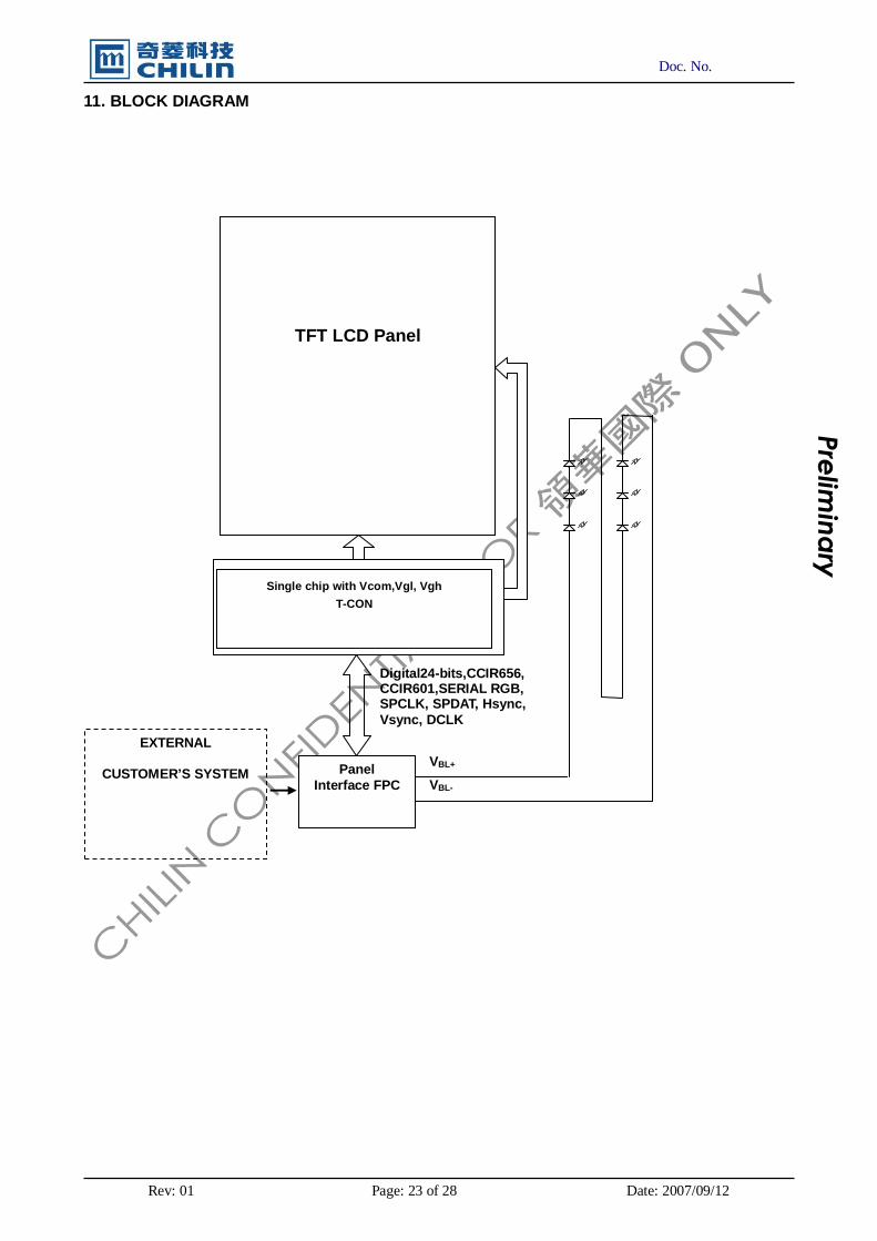
Preliminary 11. BLOCK DIAGRAM
TFT LCD Panel
Panel Interface FPC
Single chip with Vcom,Vgl, Vgh T-CON
VBL+
VBL-
EXTERNAL
CUSTOMER’S SYSTEM
Digital24-bits,CCIR656,CCIR601,SERIAL RGB, SPCLK, SPDAT, Hsync, Vsync, DCLK

Doc. No.
Rev: 01 Page: 24 of 28 Date: 2007/09/12
Preliminary 12. QUALITY ASSURANCE
No. Test Items Test Condition REMARK 1 High Temperature Storage Test Ta=80 � Dry 240h 2 Low Temperature Storage Test Ta=-30 � Dry 240h 3 High Temperature Operation Test Ta=70 � Dry 240h 4 Low Temperature Operation Test Ta=-20 � Dry 240h
5 High Temperature and High Humidity Operation Test Ta=60 90%RH 240h�
6 Electro Static Discharge Test Contact/Air: ��KV/�8KV 150PF330�
7 Shock Test (non-operating)
S h oc k L ev el : 1 0 0 G W av ef orm : H al f S i nu s oi d al W av e S h oc k T i m e : 6m s N u m b er of S h oc k s : 3 ti m es f or eac h ± X , ± Y , ± Z d i rec ti on
8 Vibration Test (non-operating)
F req u enc y rang e: 1 0 H z ~ 5 5 0 H z S tok e� 1 . 3m m S weep : 1 . 5 G, 33. 3~ 4 0 0 H z Vibration : Sinusoidal Wave, 1Hrs for
X,YZ direction.
9 Thermal Shock Test -20 (0.5h) ~ � 70�(0.5h) / 100 cycles
***** Ta= Ambient Temperature Note: 1. The test samples have recovery time for 2 hours at room temperature before the function check. In the standard
conditions, there is no display function NG issue occurred.
2. All the cosmetic specifications are judged before the reliability stress.
Doc. No.
Rev: 01 Page: 25 of 28 Date: 2007/09/12
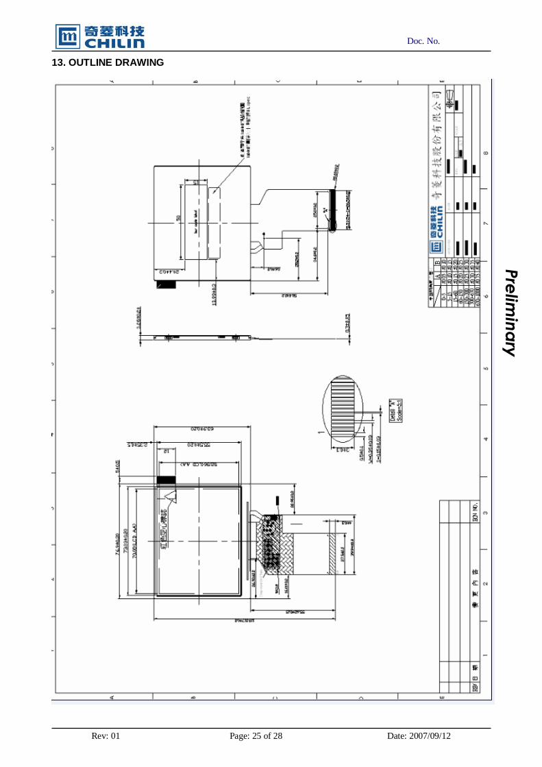
Preliminary 13. OUTLINE DRAWING
Doc. No.
Rev: 01 Page: 26 of 28 Date: 2007/09/12
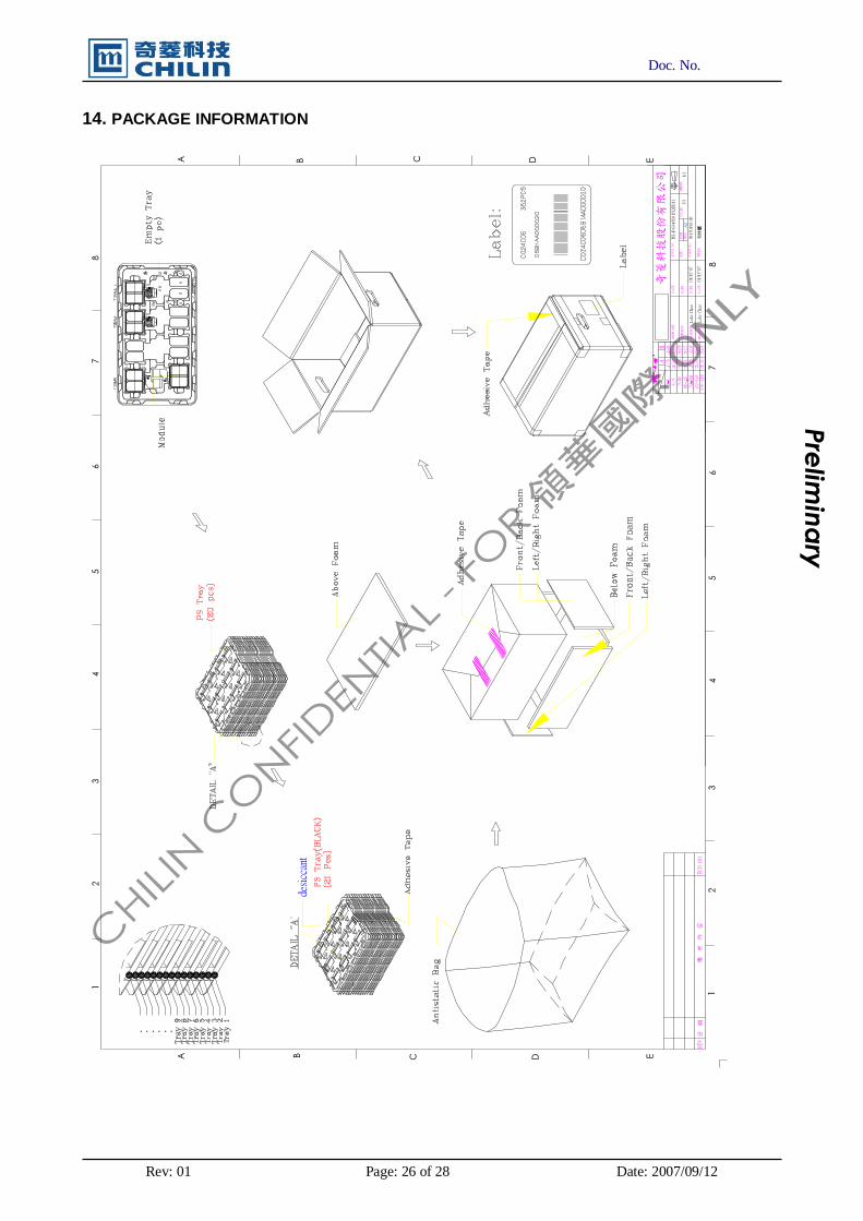
Preliminary 14. PACKAGE INFORMATION
����� � ���
����
E
1
DCBA
���
����
��
��
2�����
�
34
5
12
34
5
��������
����
�������
����
��
��
��
��
�
6
������
7 �����
�������
������
���
���
8
���
���
��
���
���
�����
�����
EDCBA
67
8
���������
�������
�������
�� �����
�� �����
���
� �
��������
����������
��������
���
��
�
Doc. No.
Rev: 01 Page: 27 of 28 Date: 2007/09/12
Preliminary 15 RECAUTIONS
Please pay attention to the following when you use this TFT LCD module.
15.1 MOUNTING PRECAUTIONS (1) You must mount a module using arranged in four corners or four sides. (2) You should consider the mounting structure so that uneven force (ex. Twisted stress) is not
applied to the module. And the case on which a module is mounted should have sufficient strength so that external force is not transmitted directly to the module.
(3) Please attach a transparent protective plate to the surface in order to protect the polarizer. Transparent protective plate should have sufficient strength in order to the resist external force.
(4) You should adopt radiation structure to satisfy the temperature specification. (5) Acetic acid type and chlorine type materials for the cover case are not describe because
the former generates corrosive gas of attacking the polarizer at high temperature and the latter causes circuit break by electro-chemical reaction.
(6) Do not touch, push or rub the exposed polarizers with glass, tweezers or anything harder than HB pencil lead. And please do not rub with dust clothes with chemical treatment. Do not touch the surface of polarizer for bare hand or greasy cloth. (Some cosmetics are determined to the polarizer)
(7) When the surface becomes dusty, please wipe gently with adsorbent cotton or other soft materials like chamois soaks with petroleum benzene. Normal-hexane is recommended for cleaning the adhesives used to attach front / rear polarizers. Do not use acetone, toluene and alcohol because they cause chemical damage to the polarizer.
(8) Wipe off saliva or water drops as soon as possible. Their long time contact with polarizer causes deformations and color fading.
(9) Do not open the case because inside circuits do not have sufficient strength.
15.2 OPERATING PRECAUTIONS (1) The spike noise causes the mis-operation of circuits. It should be lower than following
voltage�V=±200mV(Over and under shoot voltage) (2) Response time depends on the temperature. (In lower temperature, it becomes longer.) (3) Brightness depends on the temperature. (In lower temperature, it becomes lower)
And in lower temperature, response time (required time that brightness is stable after turned on) becomes longer.
(4) Be careful for condensation at sudden temperature change. Condensation makes damage to polarizer or electrical contacted parts. And after fading condensation, smear or spot will occur.
(5) When fixed patterns are displayed for a long time, remnant image is likely to occur. (6) Module has high frequency circuits. Sufficient suppression to the electromagnetic
interference shall be done by system manufacturers. Grounding and shielding methods may be important to minimize the interference.
15.3 ELECTROSTATIC DISCHARGE CONTROL Since a module is composed of electronic circuits, it is not strong to electrostatic discharge. Make certain that treatment persons are connected to ground through wristband etc. And don’t touch interface pin directly.
15.4 PRECAUTIONS FOR STRONG LIGHT EXPOSURE Strong light exposure causes degradation of polarizer and color filter.
Doc. No.
Rev: 01 Page: 28 of 28 Date: 2007/09/12
Preliminary 15.5 STORAGE
When storing modules as spares for a long time, the following precautions are necessary.
(1) Store them in a dark place. Do not expose the module to sunlight or fluorescent light. Keep the temperature between 5� and 35� at normal humidity.
(2) The polarizer surface should not come in contact with any other object. It is recommended that they be stored in the container in which they were shipped.
15.6 HANDLING PRECAUTIONS FOR PROTECTION FILM
(1) When the protection film is peeled off, static electricity is generated between the film and
polarizer. This should be peeled off slowly and carefully by people who are electrically grounded and with well ion-blown equipment or in such a condition, etc.
(2) The protection film is attached to the polarizer with a small amount of glue. Is apt to remain on the polarizer.Please carefully peel off the protection film without rubbing it against the polarizer.
(3) When the module with protection film attached is stored for a long time, sometimes there remains a very small amount of glue still on the polarizer after the protection film is peeled off.
(4) You can remove the glue easily. When the glue remains on the polarizer surface or its vestige is recognized, please wipe them off with absorbent cotton waste or other soft material like chamois soaked with normal-hexane.