LPII80 MODULE - Electrojumble · -I.F. AMPLIFIER MODULE QUICK REFERENCE DATA LPII80 ... 4 Emitter...
38
R.F. -I.F. AMPLIFIER MODULE QUICK REFERENCE DATA LPII80 This module Is a fully screened, transistorised 1.1". amplifier and mixer (without oscillator coils) for usc in radios covering long, medium and short wave banda, Supply voltage I. F. frequcm:y Sensitivity, for 50mV output Bandwidth, at 3dR points +7.6 470 1.8 5 v kHz CASING The assembly is encased in a metal can for screening and protection. TERJliUNATlONS solder pins on 3.81mm (0.15 in) pitch. SPECIAL H:ATURES Good selectivity and low thermal drift due to the usc of a ceramic resonator. Mullard DECEr..lBEH lU70 LPl180 Page 1
-
Upload
nguyenlien -
Category
Documents
-
view
226 -
download
0
Transcript of LPII80 MODULE - Electrojumble · -I.F. AMPLIFIER MODULE QUICK REFERENCE DATA LPII80 ... 4 Emitter...

R.F. -I.F. AMPLIFIERMODULE
QUICK REFERENCE DATA
LPII80
This module Is a fully screened, transistorised 1.1". amplifier and mixer(without oscillator coils) for usc in radios covering long, medium and shortwave banda,
Supply voltage
I. F. frequcm:y
Sensitivity, for 50mV output
Bandwidth, at 3dR points
+7.6
470
1.8
5
vkHz
CASING
The assembly is encased in a metal can for screening and protection.
TERJliUNATlONS
~) solder pins on 3.81mm (0.15 in) pitch.
SPECIAL H:ATURES
Good selectivity and low thermal drift due to the usc of a ceramic resonator.
MullardDECEr..lBEH lU70 LPl180 Page 1

DIMENSIONS (mill!metres)
60
I'n 7 I !
. I---- ---'
I, 40.3 ' ", t'0 _I ags 2.1)( 5 h,0---'" be bent d W Ich mayown fo r mounting
o~ 0
l-r-=~=3("1.3mQ>LlJ ~~"'O
Pie rein, d log ram
J. mal(~J~ ~_mOdule outlineT., =:- _~._----~ 3.81, ,ILI .~. 76' f-~I -----'1- 15.24 I I
... ,1 ".os
tm_CCCC_n::~~ I. I.62.23 J 9 holes ¢ 1.3 min,
D226Q
millimetrcs
inches
3.81
0.15
7.62
0.3
15.24
0.6
19.05
0.75
22.86
6.9
MullardLP1l80 Page 2

R.F. -I.F. AMPLIFIERMODULE
ELECTRICAL DATA
LPII80
Unless otherwise specified, all characteristics apply at an ambient temperature of20 .:I:50 C, atmospheric pressure of lOOOmbars and a relative humidity of 75% max.
Conditions Value
Supply voltage design +7.6V
absolute mu.ximum +9V
Supply current - 5mA
Centre frequency - 470kHz
Tolerance on frequency - ±2kHz
Bandwidth at -3d8 points 5 ::I: 1kHz.
Selectivity at -30dB points ±9kHz
at 470kHz \~ith 400Hz forSensitivity 30% modulation and a O.Olf.tF
1.BIJ.V ± 7dB(for 50mV output) capacitor in parallel with a
lOkfl resistor for load output
Signal to noise level as sensitivity >lOdB
A.G,C. - 35dB
Maximum ambient BoDetemperature -
CONNECTIONS
1sl I.F.
2nd LF.
7
•L P 1180BR
VltW 01 module: top
t23
Pin Function
1 See circuit diagrams
2 1st I. F. transforfficl'
3 Screening can
4 Emitter of 1st stage transistor
5 Input
6' Input earthyNep;ative suppty
7 Positive supply
8 Output
12~ Output earthy
.. Pins 6 and 12 are internally connected
MullardLPIIRO Page :1

ASSOCIATED CIRCUITS
l---o---+ve supplyI 7
~outpUI
I •IIIIII--o--ve supply
12
LPllBO
r------- -
(J=;J2 I
.F ~ I =6 ~pol.1 0--1,
II I ' II
I I5 !I
L_ ___ ...J 6
01590
Inductively coupled oscillator circuit (continuous tuning)
---- - l--o-+ve supply
I 7
~output2 I I •
I~I
LP11BO I/ // , I I
// 5 I
/ I~-ve supply
L __ ---I 6 ---- - 12
Colpitts type oscillator circuit (push button tuning) 01591
:: MOUNTING
The module can be mounted by means of its termination pins or by the4 tags provided.
HANDLING NOT ES
(a) The module may be soldered directly into a circuit using either a solderingiron or a solder bath. The soldering temperature must not exceed 245°C and thesoldering time must be less than 5 seconds.
(b) If it is dosired to bend the terminations, extreme care must be taken to preventdamage to the printed circuit of the module.
(0) All soldering irons and input signal supplies should be earthed to prevent breakdown of the transistors.
MullardLP1180 Page 4

R.F.-I.F. AMPLIFIERMODULE
QrnCK REFERENCE DATA
LP1181
This module' is a fully screened, transistorised i. f. amplifier and mixer(without oscillator coils) for usc in radios covering long, medium and shortwavebandR.
Supply voltage +7.6 V
I. F. f:requency 470 kHz
SeJlfCdlivity, for 50mV output l.8 pV
Bandwidth, at 3dB points S kHz
..
CASING
-_ ......... _~-- ...
The assembly is encased it~ a metal call for screening and protcctio,n.
TERMINATIONS
12 solder pins on 3. HImill (0. 15 in) pitch.
SPECIAL FEATURES
Good Rclectiviry and low thermal drift due to the IlSC of a ceramic resonator.
MullardOCTOBER 1971 LP1181 Page 1

DIMENSIONS (millimetre::;)
r23.022.7
L-'C+----------;=:>O~I, tags 2.1)(5 which mal'
1.---- 1,0.3 ------.i be bent down lor mounting1,0.0
-f
~ 0
Piercing diagram
o ~
6.610.4
L ~modult outline 3.81,""',. E------------------j , I
1- .~.--.- .. - ~~~.... -- "-- . - . -~ - 7.62 ..., ... , I
. -----__ -----4 15'" [I 't 19.05 22.86
:----.:=---~:==t l IE '-----=-- ---~ ----~- =---=-=-=- i'--12 noles 01.3 min.
--~- 62.23 -.;
0332]
millirnctres 3. gl 7.62
inches O. 15 0.3
15.24 19. OS 22. H6
0.6 0.75 0.9
Mullard------LP1l81 Page 2

R,F.-I.F. AMPLIFIERMODULE
LP1181
ELECTRICAL DATA
-
Characteristic Conditions Value
Supply voltagedesign +7.6V
absolute maximum +9V
Supply current - SmA
Centre frequency - 470kHz
Tolerance on freQuency - :!:2kHz
D..1.ndwldth at ·3dB points • ::> ± 1kHz
Selectivity at -3OdB points ±9kl-lz
Sensitivityfjn=470kHz, modulation=3(Yfo
(for SOnN output)(400Hz). outputload=O.Ol/-lF 1.8p.V ± 7dBin parallel with lOkfl.
Signal to noise level as sensitivity :>10dl1
A.G.C. (see note) 39kQ hetween pins 9 and 11 35dB
Maximum ambient - 60°Ctemperature
Unless otherwise specified, all ch,nucteristics apply at an ,ambient' temperature of20 +SoC atmospheric pressure of lOSN/m 2 and a relative humidity of 75% max
Note: The 35d8 figure is obtained in a closed loop a.g. c. system, with a 39kQ resistorconnected between pin.'l 9 and 11. If required, the a. g. c. output from pin 9 may belIsed instead to control a separate r.£. stage; in rhls case the gain of the LPlt81may also be controlled by this output, or set by two suitable biasing resistors. onebetween pins IQand 11, the other between pins It and r2.
Pin Function Pin Function
1 See ASSOCIATED CIRCUITS 7 +ve supply
2 1st i. f. tcansformer H Output
3 Screening can 9 A.G.C. output
4 Emitter of 1st stage transistor 10 Decoupled +ve bias supply
S Input 11 Base of brain contT,ol transistor
'6 Input earthy and -ve supply '12 Output ea rthy
"'Pins 6 and 12 are internally connected
MullardLP1181 Page 3

ASSOCIATED CIRCUITS
r - - - ~+Vl! SupplyI 7
~output
I 8~o..gt. output
LPl1Bl 9l-..o---+\ll! bias supplyI 10~ bosl! 01 gainI 11 control transistor
L....o- -VI! suppty1- ---l12
r- .--
cr==B1 1
.c :; :: I :~ ~pol ,I I D--1, ,
I, I
I I5 II
'-- ___ -1 ,
Ron
oms
Inductively r.:ollpled oscillator circuit (continuous tuning)
- ~+Vf: sUPplyI 7
~ output.
I 8r;;r-- ag,t. output
LPllB1 9l-..o---~Vl! bias supplyI 10
baSI! of gain~ control transistorIr--O--- _V( supply
_-J 12.
I
P,·3 1.-1
, I
r---L:=J--o--;'
I II
II
I
L - -I
03326
Colpitts type oscillator circuit (push button tuning)
MOUNTING
The module can re mOlmted by means of its termination pins or by the 4 tags provided.
HANDLlNG NOTES
(a) The module may be soldered directly into a circuit using either a s'oldering ironor a solder b'1th. The soldering temperature mUb't not'exceed 24~oC and thesoldering time must be less lhan 5 seconds.
(b) If it is desired lo bend the terminalions, extreme care must bfJ lakfJl1 to prevenrdamage to the printed circuit of the module.
(c) All soldering irolls and input signal supplies should be earthed to prevel\tbreak~
down of the transistors.
MullardLPl181 Page 4

STEREO PRE-AMPLIFIERMODULE
LP1183/2
QUICK REFERENCE DATA
Duat-input module designed for usc from ::l positive supply line with stereosystems using ceramic or low input crystal pick -up heads.
Supply voltage
Frequency response (at -3dB points)
Sensitivity for lSOmV output at 1kHz
input 1
input 2
Bass unci treble control ranges
+24
20Hz to 25kHz
110
240
±14
v
mV
mV
dB
CONSTRUCTION
Discrete COlllpoocnts assembled on to:1 printed wiri~g board.
TERMINAl' IONS
22 solder pins arranged 1.6 Oll one side and 6 on the other, using u 5. 080uo (0.2 in)pitch.
MAY 1972Mullard
LP1183/2 Page 1

",,<I
DIMENSIONS (millimetres)
I "m" dL '5 ro--- 7S 37 ---- ".
_ --.l I -110·\6 -
1] T-t- . I 1
3620 i -A- _ :::=! = ~32
,,,:'l09 L l --r -J60"
L~ -t=---- -----1- - ,,=
- _t=e== I ~j1- - - --+-:-- -
22 ,,''', ,;", L.!..I~,---- ---" J~O.S~7minon 5.08fO.2inlpitch 6 mountins holes f/J3
I II " "1 j mo'
.J t 8mo~·tI
ELECTRICAL DATA
Unless otherwise specified, all characteristicfl apply at an ambient temperature of20 ±50C, abnospheric pressure of lOSN/m2 and a relative humidity of 75% max.
Conditions Value
Supply voltage (d. c. )design +24V
absolute maximum +27V
'Supply current - O.6mA
Input impedance - sec fig. 1
Recommended volume control *external potentiometer 2QkU log
Frequency response at -3dB points 20Hz to 25kHz
Bass control range60Hz with * external
-14 to +l4dB500kn linear potentio,meter
Treble control range16kHz with "'external
~14 lo +.14dB250kQ linear potentiometer
Recommended balance control *cxternal potentiometer SOkQ linear
Sensitivity 1kHz and 15QmV outputinput 1 llOmV
input 2 240mV
Distortion lkl1z and 150mV output <0. J%
Max. ambient temperature - SOoC
*Sce ASSOCIATED CIRCUITS figure 2.
MullardLP1183/2 Page 2

STEREO PRE·AMPLIFIERMODULE
CONNECTIONS
LP1183/2
,s•
A
B
Print side of module
7
•910111213
"15I.17
"19202122
02980
Pin Connection Pin Connection
1 Input I (A) 12 Output (A)2 Input 2 (A) 13 *Supply negative (A)3 .... Input common (A) 14 Supply positive (A)4 Input 1 (B) 15 Bass control max. (B)5 Input 2 (B) 16 Treble control max. (B)
·"'(oput common (B) 17 Bass + treble wiper common (8)7 Bass contTol max. A) 18 Uass control min. B
8 Treble control max. (A) 19 . Treble control min. (0)9 Bass + treble wiper common (A) 20 Output' (B)
10 Bass control min. (A) 21 '"*Supply neg-dtive (8) ,11 Treble control min. (A) 22 Su~ply positive (8)
"Pins 3 and 13 are internally connected"Pins 6 and 21 are internally connected
MOUNTING
By the six c;i.13mm holes provided: insulated fixings arc recommended. Alternatively.the modtlle may be directly mounted by its pinE>.
HANDLING NOTES
(a) The module maybe soldered directly into a circuit using either a soldering Ironor a solder bath. TIle Rolderlng tempcraruremust not exceed 245°C; the soldering time must be Jess than' 5 seconds.
(b) If 11: Is necessary to bend the terminations. extreme care must be taken to prc- vent damage to the printed circui.t of the module.
(c) All soldering irons and input signal supp.lies should be ea rthed to prevent breakdown of the transistors.
MullardLPl183/2 Page 3

ASSOCIATED CIRCmTS
560kn D334~
1(4) IMn 10nF
':51 : rInputs 2,2Mn
3(6)
7(15)
Fig. 1. Module input circuit
Bass Trebley control l-I control
SOOk!) 250kfllinear linear
'0)
9 (17)
B (l61
11 (19)
10 (181
03H3
Balancecontrol50knlinear
Channel B Channel A r - - - - - -r---I volume r---I volume
control control I20knlog. 20knlog. I
II
.1:
Ibl
20
12
-ve supply
13
21
Outputchannel A
Outputchannel B
'""Figure 2. (a) treble and bass control ci:T:cuit connections channel A (Channel tl)
(b) stereo balance and volume control circuit connections, both channels
------Mullard------LPI H13/2 Page 4

STEREO PRE·AMPLIFIERMODULE
QUICK REFERENCE DATA
LP1184j2
Featuring very low distortion, the LP1184/2 has been designed with (our inputsfor use in stereo systems requiring comp~tibility with ceramic pick-ups,magnetic pick-ups, mono and stereo radio nmers.,Supply voltage
Frequency rcsp0m'le (at -3dB poims)
SensiUvlty for lSOmV output
ceramic pick -up
magnetic pick-up
mono radio
stereo radio
Bass and treble control ranges
+24
16Hz to 60kHz
85
2
60
85
±1.4
v
mV
mV
mV
mV
dB
CONSTRUCTION
Discrete components assembled on a printed-wiring board.
TERMINATIONS
38 solder pins arranged 16 on one sIde and 22 pins on the other, using a S.08mm(0.2 In) pitch.
DECEMBER 1974Mullard
LP1184/iPage 1

ELECTRICAL DATA
Unless otherwise specified, all characteristics apply at an ambient temperarure of20 ± SoC, atmospheric prcssu're of lOSN/m 2 and a relative humidity uf 75% max.
Conditions Value
design +24VSupply voltage (d. c. )
absolute maximum +Z7V
Supply current - 2.2mA
Frequency response at -3d13 points 16Hz to 60kHz
ceramic pick-up 85mVf. = 1kHz magnetic pick -up ZmV
Sensitivity (sec note I)m
V = 150mVout mono radio 6UmV
stereo radio 8SrriV
Pick -up input handling magnetic pick ~up input 40mV
prior to 'clipping' ceramic pick-up input ZV
Output level prior to - 3.3V, clipping' (see notc 2)
Total harmonic distortion f, = 1kHz, V = 150mV 0.02%In out
lntermodulation distortion magnetic pick-up 0.06% .
ceramic pick-up 1.2MQf. = 1kHz magnetic pi ck -up 40kQ
Input impedancem
V '" 150mVout mono radio 4k~1
stereo radio 1. 2MI~
Signal-to -noise ratio - 70dn
bass each channel SOOkQ linear
Recommended potentiometertreble each channel 2S0kQ linear
values volume control each channel 20kQ log
channel balance 50kQ linear
Bass a::lIltrol range measured at 60Hz -14 to +14dD
Treble control range measured at 16kHz ~14 to +14dB
Temperarurc rating maximum ambient SOOC
NOTES
1. Ducto the high sensitivity of this module on magnetic input, some form of screening may be required to prevent hum pick-up from external sources.
2. The output capability is sufficient to drive two Mullard LPl173 audio modules ina lOW stereo system.
MullardLP1l84/2 Page 2

STEREO PRE·AMPLIFIERMODULE LP1184j2CONNECTIONS AND DIMENSIONS (millimetres)
0)';76
I106.66
96.52 1116.64
- ri,0~, ------.,'1 3~
I_I-It -'-1--J. mounting 2 10.16holes fJ 3 + --+~'<3---'20.32
37 "=+---)- --- -- -!- - ,-'_t_35. 6
35 I Channel A 7• 8
33 9123 32 60.96 I 10
mo' :::: - rh'~":--L- - ::::
26 16
25 "t=--f --- ------+-- - ~~~~=--~=-=-===~,_t.~"''''l8f.8~7;:;:!;::====e6'6~_Oo.'i'====:;J;"'''::-'61i'-;(,,?',=Older pins ff 0.9 dmin on
View from component side of module Q S.OBmm(O.2inlpitch
~ Clearance required lor components t,~- - _.- -- -~ - - - - - - - - - - - i' ---• J12m~
==j='l , !
L -- - -' ,_.rl-'-'::Clearance req:iJiTed"'iOr" solder joints "......
Pin numbers Pin numberschannel A channel B
Connectionchannel A channel B
Connection
I 22 Magnetic equalisation 36 23 I3llss (-14dB)2 21 Flat equalisation 37 24 Bass (+14dB)3 20 Equalisation link point 36 25 Tone control wipers4 19 Volume wiper 35 26 Treble (+14d~)
5 18 Volume 34 27 Treble (-14dB)6 17 Mono radIo input 33 28 Output7 16 Stereo radio input 32 29 +24V supply8 15 Ceramic pick-up input 31 30 +2OV stabilised9 14 Magnetic pick-up input supply (see nore 3)
10 13 Magnetic link11' 12' Earth ·Pins 11 and 12, are internally connected.
NOTE 3: The module incorporates supply voltage dropper resistors in order to he compatible with other MuUard audio modules working on +24V supplles. Where a poorlyregulated supply is used. however. it is -recommended that the module be fed from a 20Vstabilised supply to pins 30 and 31 so avoiding the possibility of distortion due to signalclipping at high input levels.
MullardLP1184/2 page 3

MOUNTING
By the four Qj3mm holes provided; insulated fixings are recommended. Alternatively,the module may be directly mounted by its terminations.
HANDLING NOTES
(a) The module maybe soldered directly into u circuit using either a soldering ironor a solder bath. The soldering temperature must not exceed 24S oC and thesoldering time must he less than 5 seconds.
(b) If it II) necessary to bend the terminations, extreme care must be taken to prevent damage to the printed cI rl"uit of the module.
(c) All soldering Irons and input signal supplies should be earthed to prevent breakdown of the transistors.
ASSOCIATED CIRCUITS
19
Ibl
nel B)Balancecontrol50knlinear
nelA)
VolumeC'mlrols I-20knlog
18IChan
,
5(Chan
11112]
r===<5H Mono radio input
0:..:.:....:..= Stereo radio inpUt
0=-=-::-=-=0 Ceramic pick-up
Magnetic pick-up
lal
ChannelA B
22
21
20
19Volumecontrol 18
6 17
7 16
8 IS
9 "J- 10 13
II 12
DJ,n
Fj~re I. (0) switching connections for both channels(b) stereo balance and volume control Circuit connections, both cbaruwls
MullardLPl184j2 Page 4
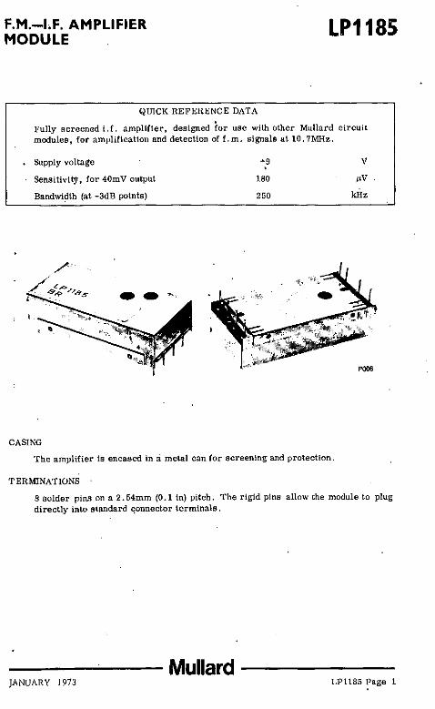
F.M.-tF. AMPLIFIERMODULE
LP1185
QmCK REFERENCE DATA
Fully screened i. f. amplifier. designed for use with other Mullard circuitmodules. for amplificatton and detection of f. m. signals at 10. 7MHz.
Supply voltago
Sensitivity, for 40mV output
Bandwi~th (at -3dB points)
+9.180
250
CASING
The amplifier is encased in a metal can for screening and protection.
TERMINATIONS
8 Bolder pins on a 2.54mm (0.1 in) pitch. The rigid pins allow the module to plugdirectly into standard qonnector terminals.
MullardJANUARY 1973 LP1185 Page 1

DIMENSIONS (m1llimetres)
fo------ 62max ------
o
-- - - - --SJ.a..j-----l
8 solder pins~0.8
~__-41.5 -I38.5
.J 0
4 tag~ 5min long l( 2.1 max widewhich may be bent down formounting·
r17
IJ_~~4.5min,
50~:'2:lf_ - -- - 56_5 -~-- -h 762::::115.24..-- I -+)._-..1. 10.6"1
I , II II, ~ ~. -rr---------- -'I
/¢--=---==--=-~-==~8hoi..Module clearance I ¢1.2min
line
Piercing diograM{view from component side of board I
Mullard
22.86(0.9in)
t
LPI185 Page 2

F.M.-I.F. AMPLIFIERMODULE
ELECTmeAL DATA
LP1185
Unless otherwise specified, all characteristics apply at an ambient temperature of20 ±SoC, an atmospheric pressure of l05N/ m2. and a relative humidity of 75%maximum. All values are measured at a supply voltage of 9V. with Ii 4. 7kQ outputload and a 22. 5kHz deviation.
Conditions Values
Supply voltage (d. c.) design +9V
absolute m~imum +lOV
Supply cprrent design 6.SmA
Centre frequency - 10. 7MHz ±50kHz
at -3dB points (10. 7MHz) 250kHzI. F. bandwidth
at -20dB points 300kHz-
Sensitivity for 40mV outputmin. 300Jl.Vmax. 60Jl.V
F. M. output at limitingImV input and output measured
180mVacross a 100kO load
Signal-ta-noise level 150Jl.V Input 60dB
'A.F.C. output ±lOOkHz off tune (open cct. volts) ±lV
A. M. rejectioninput SmV modulated 30% at 1kHz
40dB(a.m.) and 22.5kHz 400Hz (Lm.)
Maximum ambient temperature - 60°C
,..A negative going a. f .c. voltage is produced by an increase in frequency.
CONNECTIONS
3
• ···• 0 ·· ·
55
7
•
View of module base
Pin number Connections Pin number Connections
1 Input earthy 5 Supply positive2 Input 6 Audio output3 Can 7 A.F.e.4 Supply positive for tuner 8 Output earthy
Mullard------LP1185 Page 3

1st j.f.secoodary"
1st i.f.primary
Ratio detector 2nd i.! Olm
Top view of the module
MOUNl'ING
The module mllY be mOWlted into a printed wiring board by its terminations or bysuitable positioning of the four tags provided in the base tray.
TYPICAL CONNECTION DIAGRAM
nf
mo., 5 '120n , 5lO}JF •
~6 16- 6,- LP1186
~20"FLLPll 65
t-6 ~ ~"' 5k.- 7 5 22nF: ? ~
~::=1 8 1 8
.~.9
b
a
d
lOOn
* aJ.c. shown in "ON" position
External connections
nef Connection Hef Connection
a Aerial input (earthy) e Supp~y positiveb Aerial input (75Q) r Audio outputc TWling voltage (positive) g Output (earthy)d TlUling voltage (earthy)
Notes on external connections
1. The HlOnF capacitor may he required, C1epending on layout.
2. The 1QJ1.F capacitor may not be required, if the output is fed into a high impedance(100kll)
3. The 22nF capacitor is a de-emphasis component, and is not used with stereo.decoder.
HANDLING NOT ES
(a) The module may be soldered directly into 11 circuit using either a soldering trollor a solder bath. The soldel'ing temperature must not exceed ,245°C and thesoldering time must be less than 5 seconds.
(b) All soldering irons and input signal supplies should be earthed t9 prevent ureakdown of the transistors
Mullard]'P1l85 Page 4

F.M. TUNER MODULEwith diode tuning
QUICK REFEHENCE DATA
LP1186
D. C. voltage controlled hmer module designed for llaC primarily with theMulIard LP1l85 i.f. ampltfier module, in bahd II radio receivers:
Supply voltages (d. c,)
transistors
, vari-cap diodes
Frequency tuning range
Power gain (at 95MHz)
+8
+2 to +12
87.4 to 104.5
30
vv
MH/'.
dB
CASING
The module is encased in a metal can for protection and screening.
TlmMINATTONS
8 solder pins on a 2. 54mm (0.1 In) printed-wiring grid.
SPECIAL n~ATURESAND CIRCUIT DESCHIPTION
The module has three stages, a tuned aerial and r.f. stage, giving good image andI,r. rejection, a separate oscillator Rtage for good signal handling, and a mixerstage with a double-ttmcd i. f. output circuit.The use of variable capacitance diodes results in a. compact unit size, ideally suiled(or use with simple remote or local push-button pre-set tuning systems.
JANUARY 197.3Mullard
L P1l86 Page 1

DIMENSIONS (mllilmetres)
1>------- 62max .
If~---
o
_0. -----< _
8 solder pins¢O.8
41.5 _38.5
r 0 o
fI, tags 5min long x 2.1max widewhich may be bent down formounting
I17
mL_~~~l,.5min1- --
j ,;a8,~ _ _ _~6_~ b I _4mjax ! -, ---- --------------tt 5.08(O.2inl t -----,
7.62(0,3;nJ I ' --+t---r 15,21,l--n- i i _ IOrl1~29~~11I-----~---:_+t
/tr-=--=-==-=-~-=:-*8hOI'-'I.Module clearance I ¢1.2min
line
Piercing diagram(view from component side of board)
Mullard
•
LP1l86 Page 2

:.M. TUNER MODULE,ith diode tuning
;LECTRrCAL DATA
LP1186
Unless otherwise flpecified, all characteristics apply al an ambient temperature of20 ± SoC. an atmospheric pressure of 1Q5N/ m2, a relative humidity of 75% maximumwith a supply voltage of BV and a load impedance of 470Q.
Conditions Value
design +8V.supply voltage for
absolute maximum +9Vtransistors
minimum +GV
Supply voltage for diudes design 2 to 12V
Supply current, transistors - G.lmA
requeney tuning range - 87 4 to lO4.5Ml-Iz
2V tlUling voltage 87 .4MHz. ± 200kHzRange accuracy (see note 1)
12V tuning voltage 104 . 5MHz ± 500kHz
Bandwidth at - 3db points 300kHz,
Aerial impedance - 75"
Output impedance - 75Q
Centre frequency . - 10. 7MHz ± 50kHz
Oscillator stability with a .Le. disconnected60kHz/Vrespect to supply voltage f. = 95MBz
m
Oscillator st.abllity with a. f. c. disconnected-10kHz per dege riserespect to temperature 'f. '" ~5MHz
m
A.F.C.(sec note 2)Vin-±lV, f in -95l\.1H7.
±200kHzsource resistance= IDOkfl
Power gain f1n -95MHZ 30dB
Variation of power gaintypical 1dB
over tuning range maximum 6dB
Noise factor fin - 95l\.1Hz 6.5dB
Image suppression fin 95MHz 40dB
r. F. rejection fin - 9Sr.mz G5dB
Maximum ambient temperature - GOoC
DTE,S
1, Tuning range can be extended to l08l\.1Hz if a tuning voltage of approximately17V is available.
2. A negative going a. f c. voltage produces an increase in the oseillatorfrequency.
MullardLP1l86 Page 3

MOUNTING
The module may be mounted into a printed-wiring board by its terminations orsuitable positioning of the four tags provided in the base tray.
CONNECTIONS
4
3
2
0 0
0 0
0
0
0 0
View of module base
5
6.
7B
034
Pin Connection Pin Connection
1 A. [<'.C. 5 +ve supply
2 Tuning voltage (+ve) 6 Output
.3 Aerial input 7 Outp~t (earthy) .
4 Aerial input (earthy) 8 -ve supply and can
R,F, trimmer_.-~
Aerial trimmer
Aerial cail--
OJ<7'
HANDLING NOTES
Osc;lIator trimmer
'"R. F. cail
Tup view of the module
Oscillolor coil
991/, I
IF autllul coils
(a) The module may be soldered directly into a circuit using either a soldering inor u solder bath. The soldering temperature must not excec.d 24~oC and tfsoldering time must be less than 5 seconds.
(b) All soldering irons and input sip;nal supplies shol,lld be earthed to prevent brenldown of the transistors.
MullardLP1l8(l Pag€

OLTAGE MULTIPLYINGIODULES
QUICK REFERENCE DATA
LP1194Series
The modules generate e.h.t. and focus voltages from tine time rose pulses,to supply colour picture tubes.
V in (peak-to-peak)
Vout
(e. h. t. supply) (d. c.)
Vout
(focus supply,) (g. c.)
Circuit A
8.3
25
8.3
Circuit B
8.6
25
7. 7
kV
kV
kV
'YPE NUMBERS
LPI194/.30 - A nve capacitor, nve diode module with surge lIm.iting resistor.LP1194/40 - As LP 1194/ 30 with a clipping diode across the input.
'IMENSIONS (milllmctres)
d I.nglh
ertn<~ line
olu 00.3- -
TI 6
I+.-;j) .-@-. .
"I ~_. _.-' -' - - -'iJ-I I ,
.<p. ¢ f-..-...~
I I ,.EjJ 4' ,
~
Terminations:
I '" Input2 :::: Earth3 =Focus4 = Output
Fig. 1
OUNTING PRECAUTIONS
A separation of at least 15mm between any part of the main module hodyor its Leadand any meta 1 pa rts of the receiver is essentia 1 to avoid any capacitive discha rgccllrrent and detuning effects of the· line oytput transformer. Mounting bracketsmust he confined to the module mounting flanges.
)VEMBER 1974Mullard
LP1l94 Series Page I

ELECTRICAL DATA
Typical operating conditions (where I.l,.sed In typical application circuits A or B)
Circuit A Circuit B
Vln
(peak-to-pcak) 8.3 8.6
V (e.h.t. supply) (d.c.) 25 25 ,out
I (e.ll.t.) (d. c.) mout
I (focus) (d. c. ) 0.4 O. 1 mout
E. H. T. regulation (0 to 1. 5mA) 2 2.4 N
Lim iUng va lues
These are absolute operating conditions which must not be exceeded under all
condition.
V in (peak -to -peak)
Vout
(e.h.t.)
lout (clipping diode)
Tamb
For other limiting values see figures 2 and 3.
10.4
31. 2
2.5
60
10.8
31. 5
2.5
60
m
When used wilh 0 8.3kV ov",wind ""1 10101 out in circuit A
!oeu~)
m'
oo 10 15
Vln (ptClk.to·peaklkV
Fig. 2
Mullard
When und with 0 7kV o.trwind ~
1 IOlal oul in circuit B
loe""lm'
oo 10 15
Vln IptClk·to·ptClk
Fig. 3
LP1l94 Series Page

VOLTAGE MULTIPLYINGMODULES
TYPICAL APPLICATION CIRCUITS
LP1194Series
Circuit A
With this arrangement the AI diode may be omitted. This configuration Is shownfor tIC!' operation,
The beam circuit limiting components may be removed. if not required, and pointB connected to ea ["th.
,
r""n 4?Okil I b.am
limillng
"0 IOOnF
,.,+K.T. ------l
100nF 1.25kVlino<>rlly conlrol ,.
{~"~'~"~"~'"~i'--_~P'CI"'.tub.,9.91otnIJ>13MI'I)
lJ2MflIhl.JMJlJ
[=:;;C~"~"~"~":::J'--_~-OPiCIUf.tubo,9.gMJl(J.:I:lMfll
".,112Mnrld.JM!ll
, 3
Fig.4
LP119.H40
30,251
Fig. 5
MullardLP1l94 Series Page 3

Circuit 13
For a 7kV overwind, cotUlected to the primary. This configuration is used mainlyin 90° time tases and the circuit shown is for 90° operation.
Linearitycontrol
o,u,.
E2geZZJ103Focus
4.7MO
v
lP1194/30
+H.T
Ly
~I
A, -,-H~---'
II suppl ies ---.-++'lH--,
Fig. 6
Both configunttions shown in Figs. 4 and 6 may of course be used in either 9000:
1100 operation. The connections between the overwind ami tripler will remain thlsame for both deflection angles.
MullardlY1194 Series Page

STEREO DECODERMODULE
QUICK REFERENCE DATA
LP1400
Stereo. decoder module using frequency multiplex system for use tn f. m.stereo radio and tuner amplifier equipment.
Supply voltage (d. c.)
Channel separation, min.
Voltage gain, per channel
CONSTRUCTION
B to 18
38
9.5
I'OS1
V
d8
dB
Ie with discrete components, assembled on a prlnted wiring board.
TERMINATIONS
8 tinned pads suitable for use with a 3.180101 (0. 15in) pitch edge connector. Thepads have, 8 solder pins at (hel,r It'eads with a further pin at each corner of theopposite edge.
MullardOCTOBER 1974 LP1400 Page I

DIMENSIONS (miilimetres) AND CONNECTIONS
Connecting pads for use withO. 15io pitch edge connector
Piercing diagram(view from component side of board)
SOLDERING CONDITIONS
Pin Function
I OV (internally connected to pins 7, 10)
2 Input
3 Stereo inhibit
4 Lamp drive
5 Left output
6 Right output
7 OV (internally connected to pins 1, 10)
815V } Supply voltage (inter"" IIy connected)
9 15V
JO OV (interno lly connected to pins 1, 7)
245~C max. for 5s max,
MullardLP1400 Page 2

TEREO DECODERIODULE
t LECTRICAL DATA
LP1400
Unless otherwise specified, all characteristics apply at an ambient temperature of20 ± SoC, an atmospheric pressure of IOSra (10QUmhirs), a relative humidity of75% maximum. Measured with a supply voltage of lSV, a load lmpedance of lOOkQ,composite signa I of IVpeak -to -peak at 1kHz modulation including 35mVrms of 19kHzpnot tone with either left or right channel mod\J1ation. .
ValuesConditions
Min. Nom. Max.
upply voltage (see note I) - 8 15 - V
upply current - - 21 30 rnA
ndicator lamp drive design - - 100 rnA
oput voltage - - - 1.0 Vpeak-ro-peak
lutput voltage (see note 2) - - - 1.0 Vrrns
:hannel separation(sc€ note 3) - 38 - - dB
'olcage gain per channel(see note 3) - - 9.5 - dB
:hannell:nL.1.ncc - - - 1.0 dB
larmonk distortion IVnns output - 0.2 - %'requency response at -3dB points 20 - 15000 • Hz
[lot tone level for stereo15 - mV- -
operation rrns
Hot tone switchinghysteresis mono/stereo - - 1.0 - dB
oltage levels to switchmono (inhibited)stereo Inhibit I. 35 - 3.0 Vstereo (enabled) 0 - 0.8 V
lput current for monooverride - 13 - - "A
lput impedance - 50 ISO - kO
utput impedance(see notes 1, 2) - - 5.6 - kO
19kHz 36 - - dBItrasonic frequency 38kHz 36 - - dBrejectlo!1 75kHz - 19 - dB
77kHz - 19 - dB
MullardLPl400 Page 3

NOTES
1. For low voltage operation between JU and 13V, lUkQ resistors are requlnbetween each output and earth to prevent cUpping; this will reduce the gain tapproximately 6d13. Similarly between 8 and IOV, 3. 3kQ resistors. are requirecwith a reduction in gain to apprOXimately 3dB.
2. Each output 1s at a d. c. potential of approximately 6Vwhlch should be decoupllbefore being fed into the succeeding audio stage.
3. The module is a ligned for optimum performance when used with an i. f. amplifiewith the a ttenuation of O. 5dB at 38kHz (relative to 1kHz). For test purposes, t~
circuit of Fig. 1, Is used. Olher alignments arc possible.
5.6kO
Encoder 2.7kO 0ioo 760 Module•• pF input-
06132
ABSOLlITE RATINGS
These are absolute operating limits, which must not be exceeded under any conditlons.
Conditions Values
Supply voltage - 18V lll!l}
Supply voltage for lamp drive - 28V ma}
JndiC-ltor lamp Inrush currentsurge at switch 20V max. 200m A rna,
28V max. lUOmA lila)
Indicator lamp quiescent current - IOOmA ma)
·Mono/stereo switch controlvoltage - 3V rna,
.. Mono/stereo switch controlcurrent - 300/.LA ma}
Operating ambient temper,:!ture - wOe mil45°C trial
Storage tempel'ature - -IOoe mir'I_WOe rna>
"'These limits do not always occur simultaneously.,
MullardLP1400 Page

STEREO DECODERMODULE
Channel
(dB)
50
'0
30
20
10
LP~400
061lJ
oo 10 20 30 40 Hocl
CHANNE L SEPARATION/TEMPERATURE CHARACTERISTIC
MullardLP1400Pagc 5

\

F.M. TUNERMODULE
LPI402
QUICK REFERENCE DATA
F. M. tuner module (i. r. = 10. 7MHz), with capacitance tuning for a. m. ;designed for use with other Mullard circuit modules in radio receivers.
Supply voltage
Frequency tuning range (C" m.)
Power gain (at 95MHz)
+6.8
87.4 to 104.5
28
v
dB
CASING
The module Is encased· In a metal can for protection and screening.
TERMINATIONS
8 solder pins-and 2 solder taKS.
SPECIAL FEATURES
Tuning fOf both Lm. and a.m. is prOVided by a four scction foil dielectric gangcapacitor.
MullardOCTOBER 1974 r.;P140Z Page 1
•

DIMENSIONS (millimetres)
3 fixing holes 02burst extrudedsuitable forself tapping screws
"ma,
2 solder tags3.5 long x 2.8 wide x 0.4 thick
1 hOle 02
25 ~+---.rJ~x
6.9min
r---:-~~xI 123:9-
6 solder pins ['
.e,r+_0_',X 7long I6.00 1I .1-
5t ffi~---~:-Tr.-----IRIli1 'Yj
015410
9f55"
20
I..-,,~
1---,:05 . :I
holes (21 4.9
1- i l _L~-.l,-I-I'-=-F.bbb,i---'--7!,I 135 '!- t
286 24 j--j-
lJ=~_
View in direction 'A'
MECHANICAL DATA
Reduction gear ratio (anti-backlash type gear)
Maximum permissible torqueapplied to spindle (capacitor on end stop)
6.3:1
79 x 10-3 Nm
MullardLP1402 Page 2

F.M. TUNERMODULE
ELECTRICAL DATA
LPI402
Unless otherwise specified, all characteristics apply at an ambient temperature of20 ±SOC, an atmospheric pressure of 105 Pa (1000 mbars), a relative humIdlty of75% maximum with a supply voltage of 6. BV and a load impedance of 2. Zkf.t
Conditions Value
design +6.8VSupply voltage
limits at any temperature +4.5 to +7. BV max.
Supply current - 4.5mA
Frequency tuning range - 87.4 to 104. 5MHz
fin = 87. 4MHz ± 200kHzRange accuracy
fin 111104. 5MHz ± 500kHz
Bandwidth at -3dB (Xlints 300kHz
Aerial impedances - 75 or 300Q
, Output impedance - 900
I. F. - 10. 7MHz ± 50kHz
Oscillator stability witha.Le. disconnected 30kllz/Vrespect to supply voltage
I design range -2 to +2V' A. F . C. voltage withi respect to can fin-95MHz -350kHz +IVI (soe note 1)
fin = 95:MHz +500kHz -lV
Power gain fin =95MHz 28dB
Variation of power gain - <6dBover tuning range
"source =752, fin =87 .41fr1z 'dBNoise factor
zsource =7512, fin =951fr1z 4.8dB
Image suppression fin =95MHz 27dB
I. F. rejection f in -95MHz 50dB
Distortion in circuit see note 2
A. M. capacitancc" swing - S".5 to 288.5pF
A.M. trimmer capacitancc swing - >9pF
Maximum ambient temperature - 60°C
MullardLP1402 Page 3

J:l0TES
1. A positive going a. f. c. voltage decreases the oscillator frequency.
2. When the LP1402 module is used in conjunction with Mullard a.m./Lm. i.f.modules the tuner will handle signal1evels in excess of O. 5V without excessivedistortion.
CONNECTIONS
FM. trimmers
9
10
8
ViEW in direction 'A'(see dimensions)
65'
1.F. coiLs
N=~2'• 7S 75n n[,oonJ
.Input impedances
Pin number Connection Pin number Connection
1 75Q input 6 1. F. output eartb
2 Input earth 7 Positive supply
3 75Q input 8 A.F,e. input
4 Negative supply and can 9 A.M. oscillator capacitor
5 I. F. output 10 A.M. aerial capacilor
N. B. The tuner has been pre-aligned by our factory and only the a.m. trimmer capacitors(if a.m. section is used) require adjustment.
MOUNTING
Three fixing holes are provided I suitable for ~ 2mm self-tapping scrcw.s.
HANDLING NOTES
(a) The mod}lle may be soldered directly into a circuit using either a Boldering ironor a Bolder bath _ The soldering temperature must not exceed 245°C and thesoldering time mUl:>t be less than 5 seconds-_
(b) If it is desired to bend the terminations, extreme care must be taken to preventdamage to the printed circuit of the module.
(c) All soldering irons and input signal supplies should be earthed to prevent breakdown of the transistors.
MullardLP1402 Page 4