LPC-P1343
15
LPC-P1343 development board Users Manual All boards produced by Olimex are ROHS compliant Revision Initial, December 2009 Copyright(c) 2009, OLIMEX Ltd, All rights reserved Page 1
Transcript of LPC-P1343

LPC-P1343 development board Users Manual
All boards produced by Olimex are ROHS compliant
Revision Initial, December 2009Copyright(c) 2009, OLIMEX Ltd, All rights reserved
Page 1
INTRODUCTION
LPC-P1343 is development board with LPC1343 ARM Cortex-M3 based microcontrollers for embedded applications from NXP. LPC-P1343 featuring a high level of integration and low power consumption. This microcontroller supports various interfaces such as one Fast-mode Plus I2C-bus interface, USB, UART, SSP in-terfaces, four general purpose timers, a 10-bit ADC. On the board are available UEXT, Debug Interface, user buttons, USB device and user leds. All this allows you to build a diversity of powerful applications to be used in a wide range of applica-tions.
BOARD FEATURES
• MCU: LPC1343 Cortex-M3, up to 70 Mhz, 32 kB Flash, 8kB SRAM, UART RS-485, USB, SSP, I2C/Fast+, ADC
• Power supply circuit
• Power-on led
• USB connector and functionality
• USBC led
• Debug interface – SWD (Serial Wire Debug)
• UEXT connector
• Eight user leds
• Two user buttons
• Reset button
• Prototype area
• FR-4, 1.5 mm, soldermask, component print
• Dimensions:80x50mm (3.15 x 1.97")
Page 2

ELECTROSTATIC WARNING
The LPC-P1343 board is shipped in protective anti-static packaging. The board must not be subject to high electrostatic potentials. General practice for working with static sensitive devices should be applied when working with this board.
BOARD USE REQUIREMENTS
Cables: The cable you will need depends on the programmer/debugger you use. If you use ARM-JTAG-EW, you will need USB A-B cable.
Hardware: Programmer/Debugger ARM-JTAG-EW or other compatible programming/debugging tool if you work with EW-ARM.
PROCESSOR FEATURES
LPC-P1343 board use ARM Cortex™-M3 microcontroller LPC1343FBD48/301 from NXP Semiconductors with these features:
– ARM Cortex-M3 processor, running at frequencies of up to 72 MHz
– ARM Cortex-M3 built-in Nested Vectored Interrupt Controller (NVIC).
– 32kB on-chip flash programming memory. Enhanced flash memory accelerator enables high- peed 72 MHz operation with zero wait states
– In-System Programming (ISP) and In-Application Programming (IAP) via on-chip bootloader software.
– Serial interfaces:
- USB 2.0 full-speed device controller with on-chip PHY for device
- UART with fractional baud rate generation, modem, internal FIFO and RS-485/EIA-485 support.
- SSP controller with FIFO and multi-protocol capabilities.
- I2C-bus interface supporting full I2C-bus specification and Fast-mode Plus with a data rate of 1 Mbit/s with multiple address recognition and monitor mode.
– Other peripherals:
- 42 General Purpose I/O (GPIO) pins with configurable pull-up/down resistors and a new, configurable open-drain operating mode.
- Four general purpose timers/counters, with a total of four capture inputs and 13 match outputs.
- Programmable WatchDog Timer (WDT).
- System tick timer.
– Serial Wire Debug and Serial Wire Trace Port.
Page 3
– High-current output driver (20 mA) on one pin.
– High-current sink drivers (20 mA) on two I2C-bus pins in Fast-mode Plus.
– Integrated PMU (Power Management Unit) to minimize power consumption during Sleep, Deep-sleep, and Deep power-down modes.
– Three reduced power modes: Sleep, Deep-sleep, and Deep power-down.
– Single 3.3 V power supply (2.0 V to 3.6 V).
– 10-bit ADC with input multiplexing among 8 pins.
– 40 GPIO pins can be used as edge and level sensitive interrupt sources.
– Clock output function with divider that can reflect the main oscillator clock, IRC clock, CPU clock, Watchdog clock, and the USB clock.
– Processor wake-up from Deep-sleep mode via GPIO interrupts.
– Brownout detect with four separate thresholds for interrupt and one threshold for forced reset.
– Power-On Reset (POR).
– Crystal oscillator with an operating range of 1 MHz to 25 MHz.
– 12 MHz internal RC oscillator trimmed to 1 % accuracy that can optionally be used as a system clock.
– PLL allows CPU operation up to the maximum CPU rate without the need for a high-frequency crystal. May be run from the main oscillator, the internal RC oscillator, or the Watchdog oscillator.
– Code Read Protection (CRP) with different security levels.
Page 4

BLOCK DIAGRAM
Page 5

MEMORY MAP
Page 6
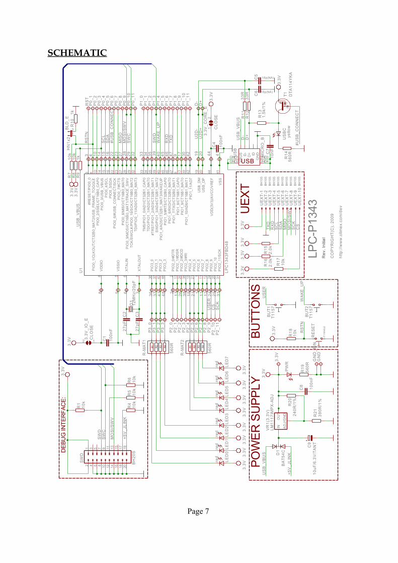
SCHEMATIC
Page 7
CLO
SE
CLO
SE
HN
1x2
T115
7
T115
7
100n
F 27pF
27pF
100n
F
18p(NA)
18p(NA)
10nF
100n
F10
uF/6
.3V
/TA
NT
BA
T54C
red
red
red
red
red
red
red
red
12M
Hz/
20pF
560R
560R
10k
10k
10k
10k
10k
10k
1k1k
33R
33R
1.5k
/1%
560R
2.0k
2.0k 10
k
10k
560R
240R
/1%
390R
/1%
IT11
85A
U2
BH
20S
DTA
114Y
KA
LPC
1343
FBD
48
BH10
SBH
10S
BH10
SBH
10S
BH10
SBH
10S
BH10
SBH
10S
BH10
SBH
10S
MIC
RO
_B
yello
w
3.3V
3.3V
3.3V
3.3V
3.3V
3.3V
3.3V
3.3V
3.3V
3.3V
3.3V
3.3V
3.3V
3.3V
3.3V
3.3V
3.3V
3.3V
3.3V
3.3V
LM11
17IM
PX
-AD
J
#US
B_C
ON
NE
CT
#US
B_C
ON
NE
CT
+5V
_JLI
NK
+5V
_JLI
NK
CS
CS
D+
D-
MIS
O
MIS
O
MO
SI/S
WV
MO
SI/S
WV
MO
SI/S
WV
RS
TN
RS
TN
RX
D
RX
D
SC
K
SC
K
SC
L
SC
L
SD
A
SD
A
SW
C
SW
CS
WD
SW
D
TXD
TXD
U2D
+U
2D-
US
B_V
BU
S
US
B_V
BU
S
US
B_V
BU
SU
SE
R
US
ER W
AK
E_U
P
WA
KE
_UP
12
3
3.3V
12
3.3V
_CO
RE
_E
12
3.3V
_IO
_E4
5 6 78
910
11 1213
14 15 16 17
18
19 20
21
22 23
24 2526
27 28 29 30
31
32 33 34 3536 37 38
39 40 4142
43
4445 46 47
48
12B
LD_E
BU
T1
BU
T2
C1
C2
C3
C4
C5
C6
C7
C8
C9
D+
D-
D1
GN
DG
ND
_PIN
LED
0LE
D1
LED
2LE
D3
LED
4LE
D5
LED
6LE
D7
P0_
1P
0_2
P0_
3P
0_4
P0_
5P
0_6
P0_
7P
0_8
P0_
9P
0_10
P0_
11
P1_
0P
1_1
P1_
2P
1_3
P1_
4P
1_5
P1_
6P
1_7
P1_
8P
1_9
P1_
10P
1_11
P2_
0P
2_1
P2_
2P
2_3
P2_
4P
2_5
P2_
6P
2_7
P2_
8P
2_9
P2_
10P
2_11
P3_
0P
3_1
P3_
2P
3_3
PW
R
Q1
R-M
AT1
R-M
AT2
R1
R4
R5
R6
R7
R8
R9
R10
R11
R12 R13
R14
R15
R16 R17
R18
R19
R20
R21
RE
SE
T
RS
T1
23
45
67
89
1011
1213
1415
1617
1819
20
SW
D
T1
#RE
SE
T/P
IO0_
03
#TR
ST/
PIO
1_2/
AD
3/C
T32B
1_M
AT1
35
PIO
0_1/
CLK
OU
T/C
T32B
0_M
AT2
/US
B_F
RA
ME
_TO
GG
LE4
PIO
0_2/
SS
EL/
CT1
6B0_
CA
P0
10
PIO
0_3/
US
B_V
BU
S14
PIO
0_4/
SC
L15
PIO
0_5/
SD
A16
PIO
0_6/
#US
B_C
ON
NE
CT/
SC
K22
PIO
0_7/
#CTS
23
PIO
0_8/
MIS
O/C
T16B
0_M
AT0
27
PIO
0_9/
MO
SI/C
T16B
0_M
AT1
/TR
AC
E_S
WV
28
PIO
1_4/
AD
5/C
T32B
1_M
AT3
/WA
KE
UP
40
PIO
1_5/
#RTS
/CT3
2B0_
CA
P0
45
PIO
1_6/
RX
D/C
T32B
0_M
AT0
46
PIO
1_7/
TXD
/CT3
2B0_
MA
T147
PIO
1_8/
CT1
6B1_
CA
P0
9
PIO
1_9/
CT1
6B1_
MA
T017
PIO
1_10
/AD
6/C
T16B
1_M
AT1
30
PIO
1_11
/AD
742
PIO
2_0/
#DTR
2
PIO
2_1/
#DS
R13
PIO
2_2/
#DC
D26
PIO
2_3/
#RI
38
PIO
2_4
18
PIO
2_5
21
PIO
2_6
1
PIO
2_7
11
PIO
2_8
12
PIO
2_9
24
PIO
2_10
25
PIO
2_11
/SC
K31
PIO
3_0
36
PIO
3_1
37
PIO
3_2
43
PIO
3_3
48
SW
D/P
IO1_
3/A
D4/
CT3
2B1_
MA
T239
TCK
/SW
CLK
/PIO
0_10
/SC
K/C
T16B
0_M
AT2
29
TDI/P
IO0_
11/A
D0/
CT3
2B0_
MA
T332
TDO
/PIO
1_1/
AD
2/C
T32B
1_M
AT0
34TM
S/P
IO1_
0/A
D1/
CT3
2B1_
CA
P0
33
US
B_D
M19
US
B_D
P20
VD
D(3
V3)
/AV
CC
/VR
EF
44
VD
DIO
8
VS
S41
VS
SIO
5
XTA
LIN
6
XTA
LOU
T7
U1
UE
XT-
1U
EX
T-2
UE
XT-
3U
EX
T-4
UE
XT-
5U
EX
T-6
UE
XT-
7U
EX
T-8
UE
XT-
9U
EX
T-10
D+D-
GN
D
GND1GND2
GND3GND4
ID
VB
USUS
B
US
BC
AD
J/G
ND
INO
UT
VR
1(3.
3V)
LPC
-P13
43R
ev. I
nitia
lR
ev. I
nitia
l
CO
PY
RIG
HT(
C),
200
9
http
://w
ww
.olim
ex.c
om/d
ev
+
R1
R2
R3
R4
R1
R2
R3
R4
10k
47
k
USB
DEB
UG
INTE
RFA
CE:
BUTT
ON
SPO
WER
SU
PPLY
UEX
T
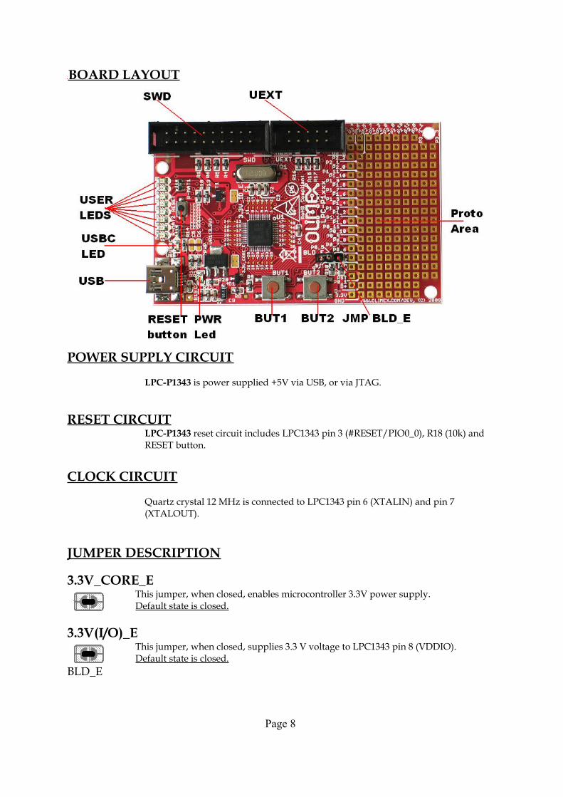
BOARD LAYOUT
POWER SUPPLY CIRCUIT
LPC-P1343 is power supplied +5V via USB, or via JTAG.
RESET CIRCUITLPC-P1343 reset circuit includes LPC1343 pin 3 (#RESET/PIO0_0), R18 (10k) and RESET button.
CLOCK CIRCUIT
Quartz crystal 12 MHz is connected to LPC1343 pin 6 (XTALIN) and pin 7 (XTALOUT).
JUMPER DESCRIPTION
3.3V_CORE_EThis jumper, when closed, enables microcontroller 3.3V power supply.Default state is closed.
3.3V(I/O)_EThis jumper, when closed, supplies 3.3 V voltage to LPC1343 pin 8 (VDDIO). Default state is closed.
BLD_E
Page 8
If BLD_E is closed during Reset and USB is connected to computer, then removable disk will be appeared in My computer. The user can
create via IAR "*.bin" file, which can be placed into the removable disk. After this when jumper BLD_E is opened during reset the microcontroller will execute program stored in "*.bin" file.
Default state is open.
INPUT/OUTPUTLED0 (red) connected via R-MAT1 to LPC1343 pin 36 (PIO3_0).
LED1 (red) connected via R-MAT1 to LPC1343 pin 37 (PIO3_1).
LED2 (red) connected via R-MAT1 to LPC1343 pin 43 (PIO3_2).
LED3 (red) connected via R-MAT1 to LPC1343 pin 48 (PIO3_3).
LED4 (red) connected via R-MAT2 to LPC1343 pin 18 (PIO3_4).
LED5 (red) connected via R-MAT2 to LPC1343 pin 21 (PIO3_5).
LED6 (red) connected via R-MAT2 to LPC1343 pin 1 (PIO2_6).
LED7 (red) connected via R-MAT2 to LPC1343 pin 11 (PIO2_7).
USBC (yellow) shows that USB is connected.
Power-on LED (red) – this LED shows that +3.3V is applied to the board.
User button with name BUT1 (USER) connected to LPC1343 pin 24 (PIO2_9).
User button with name BUT2 connected to LPC1343 pin 40 (WAKEUP).
Reset button with name RESET connected to LPC1343 pin 3 (#RESET/PIO0_0).
Page 9

EXTERNAL CONNECTORS DESCRIPTIONUEXT
Pin # Signal Name
1 3.3V
2 GND
3 TXD
4 RXD
5 SCL
6 SDA
7 MISO
8 MOSI/SWV
9 SCK
10 CS
SWD
Pin # Signal Name Pin # Signal Name
1 3.3V 2 3.3V
3 NC 4 GND
5 NC 6 GND
7 SWD 8 GND
9 SWC 10 GND
11 pull-down 12 GND
13 MOSI/SWV 14 GND
15 NC 16 GND
17 pull-down 18 GND
19 +5V_JLINK 20 GND
Page 10
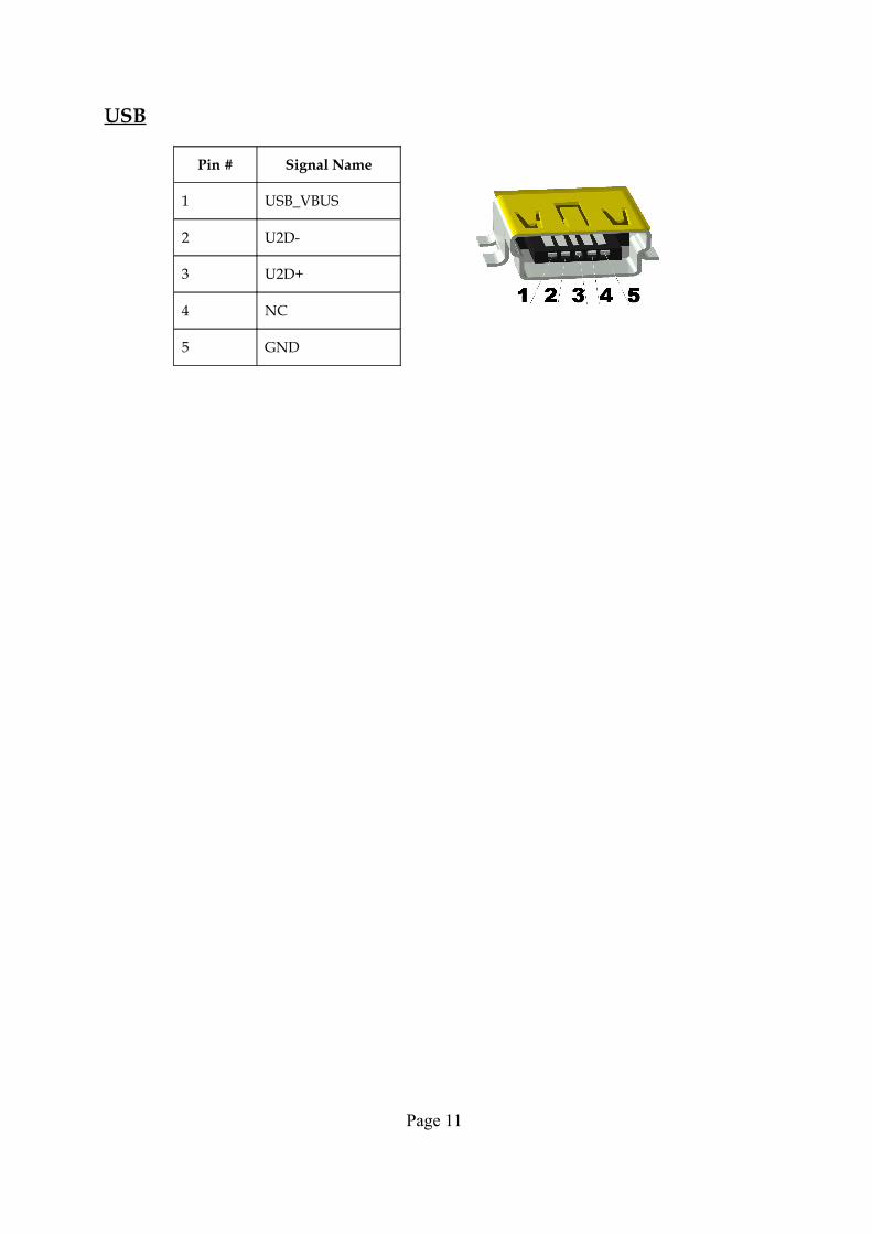
USB
Pin # Signal Name
1 USB_VBUS
2 U2D-
3 U2D+
4 NC
5 GND
Page 11
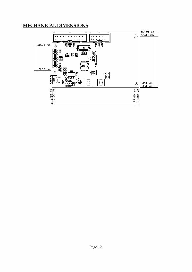
MECHANICAL DIMENSIONS
Page 12
AVAILABLE DEMO SOFTWARE
Page 13
ORDER CODELPC-P1343 - assembled and tested board
How to order?
You can order to us directly or by any of our distributors.Check our web www.olimex.com/dev for more info.
Revision history
Revision Initial, December 2009
Page 14
Disclaimer
© 2009 Olimex Ltd. All rights reserved. Olimex®, logo and combinations thereof, are registered trademarks of Olimex Ltd. Other terms and product names may be trademarks of others.
The information in this document is provided in connection with Olimex products. No license, express or implied or otherwise, to any intellectual property right is granted by this document or in connection with the sale of Olimex products. Neither the whole nor any part of the information contained in or the product described in this document may be adapted or reproduced in any material from except with the prior written permission of the copyright holder.The product described in this document is subject to continuous development and improvements. All particulars of the product and its use contained in this document are given by OLIMEX in good faith. However all warranties implied or expressed including but not limited to implied warranties of merchantability or fitness for purpose are excluded.This document is intended only to assist the reader in the use of the product. OLIMEX Ltd. shall not be liable for any loss or damage arising from the use of any information in this document or any error or omission in such information or any incorrect use of the product.
Page 15