LP5922 2-A Low-Noise Adjustable LDO w/ Low Input- … · – Radio Transceivers, Power ......
29
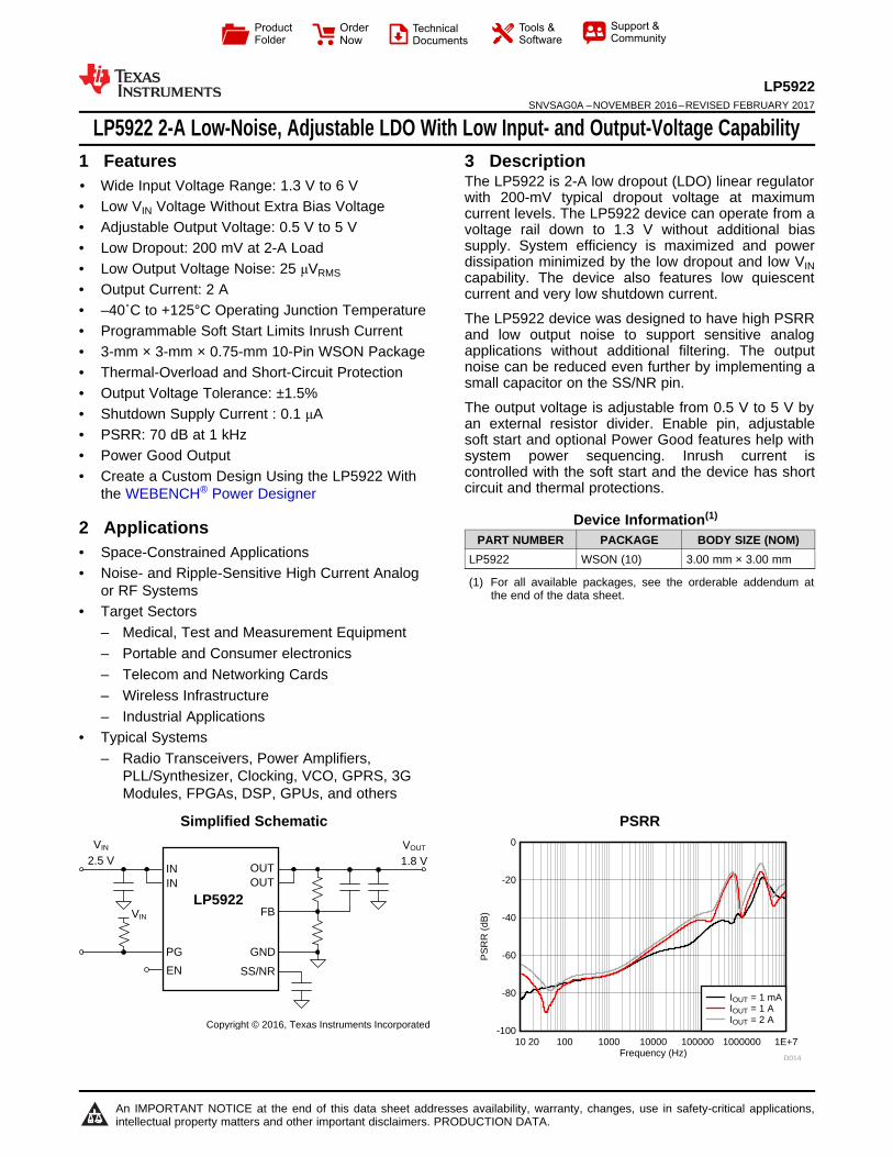
Frequency (Hz) PSRR (dB) 10 20 100 1000 10000 100000 1000000 1E+7 -100 -80 -60 -40 -20 0 D014 I OUT = 1 mA I OUT = 1 A I OUT = 2 A OUT PG V IN 2.5 V EN LP5922 V OUT 1.8 V IN GND FB SS/NR IN OUT V IN Copyright © 2016, Texas Instruments Incorporated Product Folder Order Now Technical Documents Tools & Software Support & Community An IMPORTANT NOTICE at the end of this data sheet addresses availability, warranty, changes, use in safety-critical applications, intellectual property matters and other important disclaimers. PRODUCTION DATA. LP5922 SNVSAG0A – NOVEMBER 2016 – REVISED FEBRUARY 2017 LP5922 2-A Low-Noise, Adjustable LDO With Low Input- and Output-Voltage Capability 1 1 Features 1• Wide Input Voltage Range: 1.3 V to 6 V • Low V IN Voltage Without Extra Bias Voltage • Adjustable Output Voltage: 0.5 V to 5 V • Low Dropout: 200 mV at 2-A Load • Low Output Voltage Noise: 25 μV RMS • Output Current: 2 A • –40˚C to +125°C Operating Junction Temperature • Programmable Soft Start Limits Inrush Current • 3-mm × 3-mm × 0.75-mm 10-Pin WSON Package • Thermal-Overload and Short-Circuit Protection • Output Voltage Tolerance: ±1.5% • Shutdown Supply Current : 0.1 μA • PSRR: 70 dB at 1 kHz • Power Good Output • Create a Custom Design Using the LP5922 With the WEBENCH ® Power Designer 2 Applications • Space-Constrained Applications • Noise- and Ripple-Sensitive High Current Analog or RF Systems • Target Sectors – Medical, Test and Measurement Equipment – Portable and Consumer electronics – Telecom and Networking Cards – Wireless Infrastructure – Industrial Applications • Typical Systems – Radio Transceivers, Power Amplifiers, PLL/Synthesizer, Clocking, VCO, GPRS, 3G Modules, FPGAs, DSP, GPUs, and others 3 Description The LP5922 is 2-A low dropout (LDO) linear regulator with 200-mV typical dropout voltage at maximum current levels. The LP5922 device can operate from a voltage rail down to 1.3 V without additional bias supply. System efficiency is maximized and power dissipation minimized by the low dropout and low V IN capability. The device also features low quiescent current and very low shutdown current. The LP5922 device was designed to have high PSRR and low output noise to support sensitive analog applications without additional filtering. The output noise can be reduced even further by implementing a small capacitor on the SS/NR pin. The output voltage is adjustable from 0.5 V to 5 V by an external resistor divider. Enable pin, adjustable soft start and optional Power Good features help with system power sequencing. Inrush current is controlled with the soft start and the device has short circuit and thermal protections. Device Information (1) PART NUMBER PACKAGE BODY SIZE (NOM) LP5922 WSON (10) 3.00 mm × 3.00 mm (1) For all available packages, see the orderable addendum at the end of the data sheet. space space space space space space space Simplified Schematic PSRR
Transcript of LP5922 2-A Low-Noise Adjustable LDO w/ Low Input- … · – Radio Transceivers, Power ......
Frequency (Hz)
PS
RR
(dB
)
10 20 100 1000 10000 100000 1000000 1E+7-100
-80
-60
-40
-20
0
D014
IOUT = 1 mAIOUT = 1 AIOUT = 2 A
OUT
PG
VIN
2.5 V
EN
LP5922
VOUT
1.8 VIN
GND
FB
SS/NR
IN OUT
VIN
Copyright © 2016, Texas Instruments Incorporated
Product
Folder
Order
Now
Technical
Documents
Tools &
Software
Support &Community
An IMPORTANT NOTICE at the end of this data sheet addresses availability, warranty, changes, use in safety-critical applications,intellectual property matters and other important disclaimers. PRODUCTION DATA.
LP5922SNVSAG0A –NOVEMBER 2016–REVISED FEBRUARY 2017
LP5922 2-A Low-Noise, Adjustable LDO With Low Input- and Output-Voltage Capability
1
1 Features1• Wide Input Voltage Range: 1.3 V to 6 V• Low VIN Voltage Without Extra Bias Voltage• Adjustable Output Voltage: 0.5 V to 5 V• Low Dropout: 200 mV at 2-A Load• Low Output Voltage Noise: 25 μVRMS
• Output Current: 2 A• –40˚C to +125°C Operating Junction Temperature• Programmable Soft Start Limits Inrush Current• 3-mm × 3-mm × 0.75-mm 10-Pin WSON Package• Thermal-Overload and Short-Circuit Protection• Output Voltage Tolerance: ±1.5%• Shutdown Supply Current : 0.1 μA• PSRR: 70 dB at 1 kHz• Power Good Output• Create a Custom Design Using the LP5922 With
the WEBENCH® Power Designer
2 Applications• Space-Constrained Applications• Noise- and Ripple-Sensitive High Current Analog
or RF Systems• Target Sectors
– Medical, Test and Measurement Equipment– Portable and Consumer electronics– Telecom and Networking Cards– Wireless Infrastructure– Industrial Applications
• Typical Systems– Radio Transceivers, Power Amplifiers,
PLL/Synthesizer, Clocking, VCO, GPRS, 3GModules, FPGAs, DSP, GPUs, and others
3 DescriptionThe LP5922 is 2-A low dropout (LDO) linear regulatorwith 200-mV typical dropout voltage at maximumcurrent levels. The LP5922 device can operate from avoltage rail down to 1.3 V without additional biassupply. System efficiency is maximized and powerdissipation minimized by the low dropout and low VINcapability. The device also features low quiescentcurrent and very low shutdown current.
The LP5922 device was designed to have high PSRRand low output noise to support sensitive analogapplications without additional filtering. The outputnoise can be reduced even further by implementing asmall capacitor on the SS/NR pin.
The output voltage is adjustable from 0.5 V to 5 V byan external resistor divider. Enable pin, adjustablesoft start and optional Power Good features help withsystem power sequencing. Inrush current iscontrolled with the soft start and the device has shortcircuit and thermal protections.
Device Information(1)
PART NUMBER PACKAGE BODY SIZE (NOM)LP5922 WSON (10) 3.00 mm × 3.00 mm
(1) For all available packages, see the orderable addendum atthe end of the data sheet.
space
space
space
space
space
space
space
Simplified Schematic PSRR
2
LP5922SNVSAG0A –NOVEMBER 2016–REVISED FEBRUARY 2017 www.ti.com
Product Folder Links: LP5922
Submit Documentation Feedback Copyright © 2016–2017, Texas Instruments Incorporated
Table of Contents1 Features .................................................................. 12 Applications ........................................................... 13 Description ............................................................. 14 Revision History..................................................... 25 Pin Configuration and Functions ......................... 36 Specifications......................................................... 4
6.1 Absolute Maximum Ratings ...................................... 46.2 ESD Ratings.............................................................. 46.3 Recommended Operating Conditions....................... 46.4 Thermal Information .................................................. 46.5 Electrical Characteristics........................................... 56.6 Input and Output Capacitors ..................................... 66.7 Typical Characteristics .............................................. 7
7 Detailed Description ............................................ 107.1 Overview ................................................................. 107.2 Functional Block Diagram ....................................... 107.3 Feature Description................................................. 10
7.4 Device Functional Modes........................................ 128 Applications and Implementation ...................... 13
8.1 Application Information............................................ 138.2 Typical Application .................................................. 13
9 Power Supply Recommendations ...................... 1910 Layout................................................................... 19
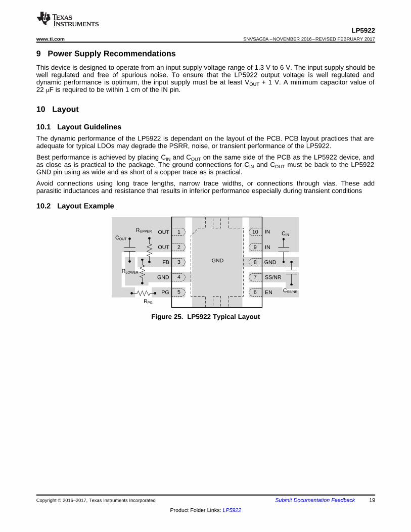
10.1 Layout Guidelines ................................................. 1910.2 Layout Example .................................................... 19
11 Device and Documentation Support ................. 2011.1 Device Support...................................................... 2011.2 Related Documentation ....................................... 2011.3 Receiving Notification of Documentation Updates 2011.4 Community Resources.......................................... 2011.5 Trademarks ........................................................... 2011.6 Electrostatic Discharge Caution............................ 2011.7 Glossary ................................................................ 21
12 Mechanical, Packaging, and OrderableInformation ........................................................... 21
4 Revision History
Changes from Original (November 2016) to Revision A Page
• Added links to WEBENCH ..................................................................................................................................................... 1• Changed load transients test conditions from "VOUT = 3.3 V" to "VOUT = 2.8 V" and "tRISE = tFALL = 1 V/μs" to "tRISE =
tFALL = 1 A/μs" ......................................................................................................................................................................... 6• Changed "tfall = 1 V/µs" to "tfall = 1 A/µs" in legend to Figure 9 ............................................................................................. 8• Changed scope shot in Figure 10 (was duplicate of Fig 9) and changed condition from "tfall = 1 V/µs" to "tfall = 1
A/µs" ...................................................................................................................................................................................... 8• Changed tfall = 1 V/μs" to "tRISE =tFALL = 5 µs" in Figure 11 conditions ................................................................................... 8• Added Custom Design With WEBENCH Tools subsection ................................................................................................. 14
OUT
GND
OUT
FB
IN
GND
SS/NR
ENPG
IN
3
1
2
4
5
8
10
9
7
6
3
LP5922www.ti.com SNVSAG0A –NOVEMBER 2016–REVISED FEBRUARY 2017
Product Folder Links: LP5922
Submit Documentation FeedbackCopyright © 2016–2017, Texas Instruments Incorporated
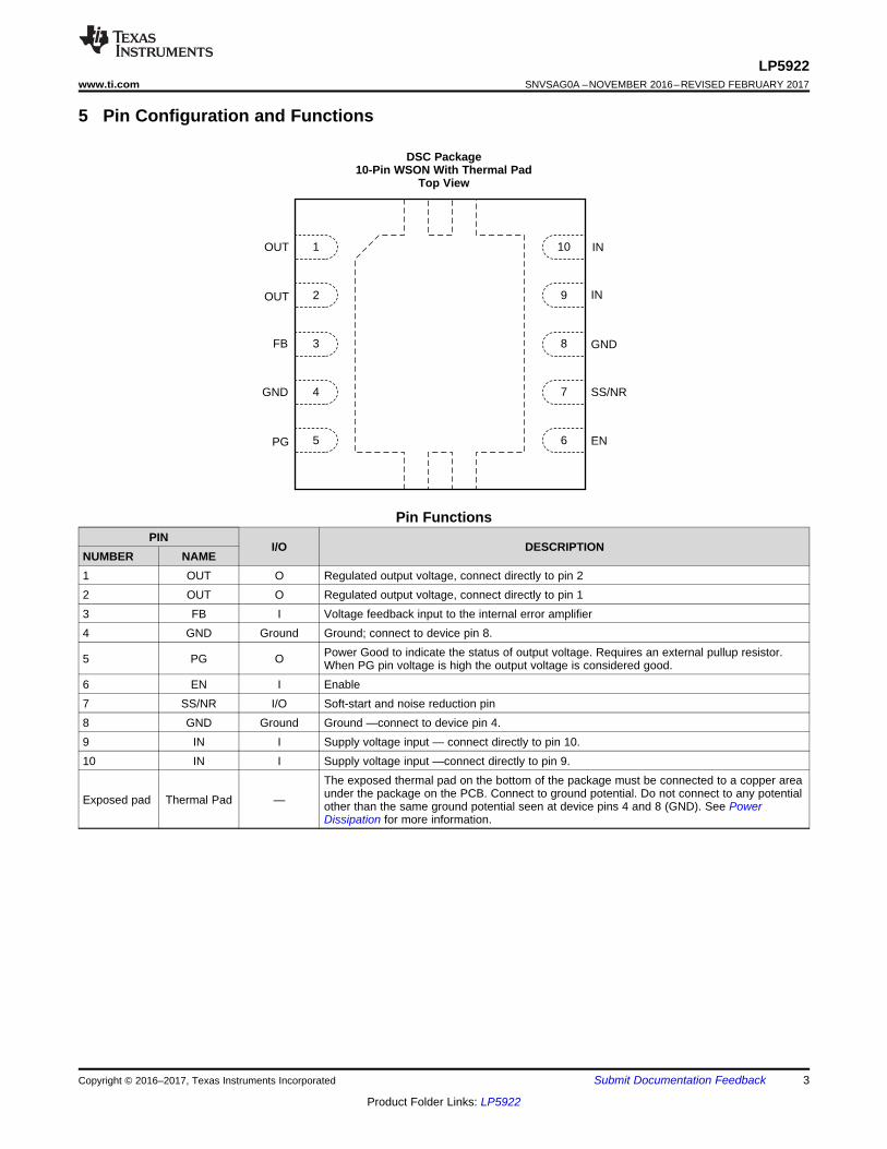
5 Pin Configuration and Functions
DSC Package10-Pin WSON With Thermal Pad
Top View
Pin FunctionsPIN
I/O DESCRIPTIONNUMBER NAME1 OUT O Regulated output voltage, connect directly to pin 22 OUT O Regulated output voltage, connect directly to pin 13 FB I Voltage feedback input to the internal error amplifier4 GND Ground Ground; connect to device pin 8.
5 PG O Power Good to indicate the status of output voltage. Requires an external pullup resistor.When PG pin voltage is high the output voltage is considered good.
6 EN I Enable7 SS/NR I/O Soft-start and noise reduction pin8 GND Ground Ground —connect to device pin 4.9 IN I Supply voltage input — connect directly to pin 10.10 IN I Supply voltage input —connect directly to pin 9.
Exposed pad Thermal Pad —
The exposed thermal pad on the bottom of the package must be connected to a copper areaunder the package on the PCB. Connect to ground potential. Do not connect to any potentialother than the same ground potential seen at device pins 4 and 8 (GND). See PowerDissipation for more information.
4
LP5922SNVSAG0A –NOVEMBER 2016–REVISED FEBRUARY 2017 www.ti.com
Product Folder Links: LP5922
Submit Documentation Feedback Copyright © 2016–2017, Texas Instruments Incorporated
(1) Stresses beyond those listed under Absolute Maximum Ratings may cause permanent damage to the device. These are stress ratingsonly, which do not imply functional operation of the device at these or any other conditions beyond those indicated under RecommendedOperating Conditions. Exposure to absolute-maximum-rated conditions for extended periods may affect device reliability.
(2) All voltages are with respect to the potential at the GND pin.(3) Absolute maximum VOUT is the lesser of VIN + 0.3 V, or 7 V.(4) Internal thermal shutdown circuitry protects the device from permanent damage.
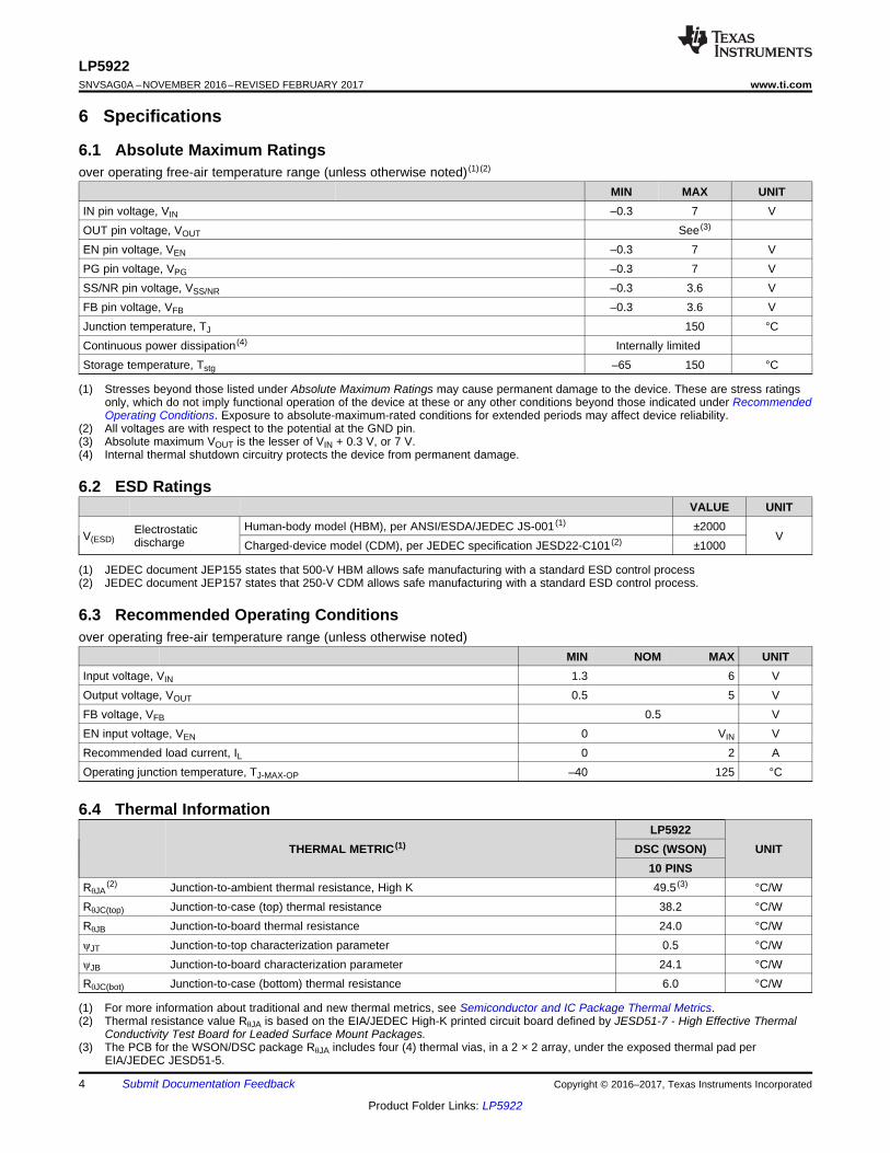
6 Specifications
6.1 Absolute Maximum Ratingsover operating free-air temperature range (unless otherwise noted) (1) (2)
MIN MAX UNITIN pin voltage, VIN –0.3 7 VOUT pin voltage, VOUT See (3)
EN pin voltage, VEN –0.3 7 VPG pin voltage, VPG –0.3 7 VSS/NR pin voltage, VSS/NR –0.3 3.6 VFB pin voltage, VFB –0.3 3.6 VJunction temperature, TJ 150 °CContinuous power dissipation (4) Internally limitedStorage temperature, Tstg –65 150 °C
(1) JEDEC document JEP155 states that 500-V HBM allows safe manufacturing with a standard ESD control process(2) JEDEC document JEP157 states that 250-V CDM allows safe manufacturing with a standard ESD control process.
6.2 ESD RatingsVALUE UNIT
V(ESD)Electrostaticdischarge
Human-body model (HBM), per ANSI/ESDA/JEDEC JS-001 (1) ±2000V
Charged-device model (CDM), per JEDEC specification JESD22-C101 (2) ±1000
6.3 Recommended Operating Conditionsover operating free-air temperature range (unless otherwise noted)
MIN NOM MAX UNITInput voltage, VIN 1.3 6 VOutput voltage, VOUT 0.5 5 VFB voltage, VFB 0.5 VEN input voltage, VEN 0 VIN VRecommended load current, IL 0 2 AOperating junction temperature, TJ-MAX-OP –40 125 °C
(1) For more information about traditional and new thermal metrics, see Semiconductor and IC Package Thermal Metrics.(2) Thermal resistance value RθJA is based on the EIA/JEDEC High-K printed circuit board defined by JESD51-7 - High Effective Thermal
Conductivity Test Board for Leaded Surface Mount Packages.(3) The PCB for the WSON/DSC package RθJA includes four (4) thermal vias, in a 2 × 2 array, under the exposed thermal pad per
EIA/JEDEC JESD51-5.
6.4 Thermal Information
THERMAL METRIC (1)LP5922
UNITDSC (WSON)10 PINS
RθJA(2) Junction-to-ambient thermal resistance, High K 49.5 (3) °C/W
RθJC(top) Junction-to-case (top) thermal resistance 38.2 °C/WRθJB Junction-to-board thermal resistance 24.0 °C/WψJT Junction-to-top characterization parameter 0.5 °C/WψJB Junction-to-board characterization parameter 24.1 °C/WRθJC(bot) Junction-to-case (bottom) thermal resistance 6.0 °C/W
5
LP5922www.ti.com SNVSAG0A –NOVEMBER 2016–REVISED FEBRUARY 2017
Product Folder Links: LP5922
Submit Documentation FeedbackCopyright © 2016–2017, Texas Instruments Incorporated
(1) All voltages are with respect to the GND pin.(2) Minimum and maximum limits are design targeted limits over the junction temperature (TJ) range of –40°C to +125°C, unless otherwise
stated. Typical values represent the most likely parametric norm at TJ = 25°C, and are provided for reference purposes only.(3) CIN, COUT: Low-ESR surface-mount-ceramic capacitors (MLCCs) used in setting electrical characteristics.(4) Dropout voltage is the voltage difference between the input and the output at which the FB voltage drops to 97% of its nominal value.(5) Short-circuit current (ISC) is equivalent to current limit. To minimize thermal effects during testing, ISC is measured with VOUT pulled to
100 mV below its nominal voltage.(6) Ground current is defined here as the total current flowing to ground as a result of all voltages applied to the device
IGND = ( (IIN – IOUT) + IEN + ILKG(PG))(7) Ground current in shutdown mode, IGND(SD), does NOT include current from PG pin.(8) This specification is verified by design.
6.5 Electrical CharacteristicsVIN = VOUT(NOM) + 0.5 V or 1.3 V, whichever is greater; VEN = 1.2 V, CIN = 22 μF, COUT = 22 μF, OUT connected to 50 Ω toGND, VFB = 0.5 V, CSS/NR = 0.12 µF, CFF = 0.01 µF, and PG pin pulled up to VIN by 100-kΩ resistor (unless otherwisenoted). (1) (2) (3)
PARAMETER TEST CONDITIONS MIN TYP MAX UNITSUPPLY VOLTAGEVIN Input voltage range 1.3 6 V
UVLO Undervoltage lock-outthreshold VIN Rising (↑) until output is ON 1.2 1.25 V
ΔUVLO UVLO hysteresis VIN Falling (↓) from UVLO threshold until output isOFF 160 mV
OUTPUT VOLTAGE AND REGULATIONVOUT Output voltage range 0.5 5 V
ΔVOUTLine regulation IOUT = 5 mA, 1.3 V ≤ VIN ≤ 6 V 0.02 %/VLoad regulation 5 mA ≤ IOUT ≤ 2 A 0.1 %/A
VDO Dropout voltage (4)
VIN = 1.4 V, IOUT = 2 A 220 400mVVIN = 2.5 V, IOUT = 2 A 100 180
VIN = 5.3 V, IOUT = 2 A 90 160FBVFB FB voltage IOUT = 5 mA to 2 A 492.5 500 507.5 mVIFB FB pin input current VFB = 0.5 V –100 100 nACURRENT LEVELSIL Maximum load current VIN ≥ 1.3 V 2 AISC Short-circuit current limit (5) 2.2 3 3.8 A
IGND
Ground-current minimumload (6) VIN = 6 V, IOUT = 0 mA 0.7
mAGround-current maximumload (6) VIN = 1.3 V, IOUT = 2 A 1 4
IGND(SD) Shutdown current (7) VIN = 6 V, VEN = 0 V, VPG = 0 V 0.1 15 µAVIN to VOUT RIPPLE REJECTION (8)
PSRR Power-supply rejectionratio
VIN ≥ 1.4 V, ƒ = 1 kHz, IOUT = 2 A 70
dBVIN ≥ 1.4 V, ƒ = 10 kHz, IOUT = 2 A 55VIN ≥ 1.4 V, ƒ = 100 kHz, IOUT = 2 A 40VIN ≥ 1.4 V, ƒ = 1 MHz, IOUT = 2 A 30
OUTPUT NOISE VOLTAGE
eN Noise voltage (8) VIN= 2.5 V, VOUT= 1.8 VBW = 10 Hz to 100 kHz 25 µVRMS
6
LP5922SNVSAG0A –NOVEMBER 2016–REVISED FEBRUARY 2017 www.ti.com
Product Folder Links: LP5922
Submit Documentation Feedback Copyright © 2016–2017, Texas Instruments Incorporated
Electrical Characteristics (continued)VIN = VOUT(NOM) + 0.5 V or 1.3 V, whichever is greater; VEN = 1.2 V, CIN = 22 μF, COUT = 22 μF, OUT connected to 50 Ω toGND, VFB = 0.5 V, CSS/NR = 0.12 µF, CFF = 0.01 µF, and PG pin pulled up to VIN by 100-kΩ resistor (unless otherwisenoted).(1)(2)(3)
PARAMETER TEST CONDITIONS MIN TYP MAX UNIT
(9) There is a 2-MΩ resistor between EN and ground (pulldown) on the device.
LOGIC INPUT THRESHOLDSVIL(EN) EN pin low threshold VEN falling (↓) until output is OFF 0.35 VVIH(EN) EN pin high threshold VEN rising (↑) until output is ON 1.2 VIEN Input current at EN pin (9) VIN = 6 V, VEN = 6 V 3 µA
PGHTHPG high threshold (% ofnominal VOUT) VOUT rising (↑) until PG goes high 94%
PGLTHPG low threshold (% ofnominal VOUT) VOUT falling (↓) until PG goes low 90%
VOL(PG)PG pin low-level outputvoltage VOUT < PGLTH, sink current = 1 mA 400 mV
ILKG(PG) PG pin leakage current VOUT > PGHTH, VPG = 6 V 1 µASOFT START
ISSSS/NR pin chargingcurrent 6.2 µA
THERMAL SHUTDOWN
TSDThermal shutdowntemperature 165 °C
ΔTSDThermal shutdownhysteresis 15 °C
TRANSITION CHARACTERISTICS
ΔVOUT
Line transients ΔVIN = 0.5 V, VOUT = 2.8 V,tRISE = tFALL = 5 μs 3
mVLoad transients VOUT = 2.8 V, IOUT = 10 mA to 2 A to 10 mA
tRISE = tFALL = 1 A/μs 25
RADOutput discharge pull-down resistance VEN = 0 V, VIN = 2.3 V 400 Ω
(1) Typically input capacitance placed close to the device is in the same order as output capacitance. See also Input Capacitor, CIN.
6.6 Input and Output Capacitorsover operating free-air temperature range (unless otherwise noted)
PARAMETER TEST CONDITIONS MIN TYP MAX UNITCIN Input capacitance (1) 22 µF
COUT Output capacitanceVOUT ≤ 0.8 V 34 47
µFVOUT > 0.8 V 15 22
Time (ms)
Vol
tage
(V
)
VS
SIN
R V
olta
ge (
V)
-5 0 5 10 15 20 25 30 35 40 45 500 0
0.5 50
1 100
1.5 150
2 200
2.5 250
3 300
3.5 350
4 400
4.5 450
5 500
5.5 550
D010
VIN,VENVOUTVSS/NRVPG
Time (ms)
Vol
tage
(V
)
VS
S/N
R V
olta
ge (
V)
-5 0 5 10 15 20 25 30 35 40 45 500 0
0.6 60
1.2 120
1.8 180
2.4 240
3 300
3.6 360
4.2 420
4.8 480
5.4 540
6 600
D011
VIN,VENVOUTVSS/NRVPG
Time (ms)
Vol
tage
(V
)
VS
S/N
R V
olta
ge (
V)
-2 0 2 4 6 8 10 12 14 16 180 0
0.5 50
1 100
1.5 150
2 200
2.5 250
3 300
3.5 350
4 400
4.5 450
5 500
5.5 550
D008
VIN, VENVOUTVSS/NRVPG
Time (ms)
Vol
tage
(V
)
VS
S/N
R V
olta
ge (
V)
-2 0 2 4 6 8 10 12 14 16 180 0
0.5 50
1 100
1.5 150
2 200
2.5 250
3 300
3.5 350
4 400
4.5 450
5 500
5.5 550
D009
VIN,VENVOUTVSS/NRVPG
Input Voltage (V)
VE
N T
hres
hold
(V
)
1 1.5 2 2.5 3 3.5 4 4.5 5 5.5 60.3
0.4
0.5
0.6
0.7
0.8
0.9
1
1.1
1.2
1.3
D007
VEN(ON)VEN(OFF)
IOUT (A)
I GN
D (
mA
)
0 0.2 0.4 0.6 0.8 1 1.2 1.4 1.6 1.8 20.5
0.75
1
1.25
1.5
1.75
2
2.25
2.5
2.75
3
3.25
3.5
D017
VIN = 5.5 V, VOUT = 5.0 V
7
LP5922www.ti.com SNVSAG0A –NOVEMBER 2016–REVISED FEBRUARY 2017
Product Folder Links: LP5922
Submit Documentation FeedbackCopyright © 2016–2017, Texas Instruments Incorporated
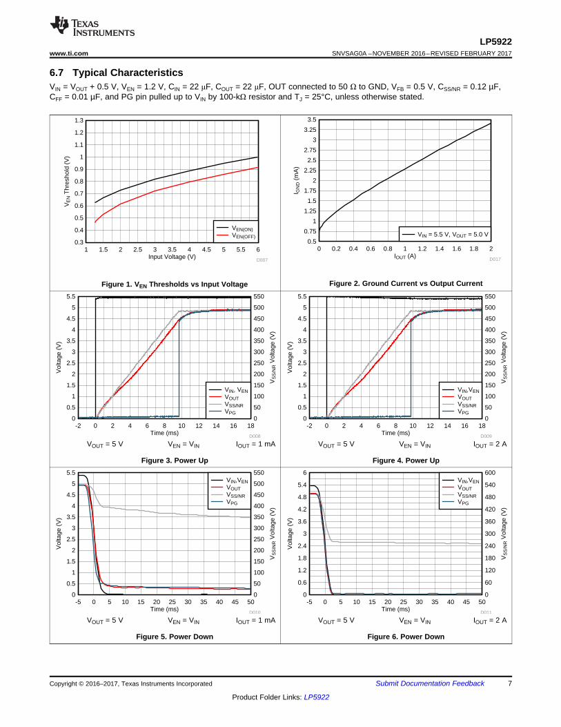
6.7 Typical CharacteristicsVIN = VOUT + 0.5 V, VEN = 1.2 V, CIN = 22 μF, COUT = 22 μF, OUT connected to 50 Ω to GND, VFB = 0.5 V, CSS/NR = 0.12 µF,CFF = 0.01 µF, and PG pin pulled up to VIN by 100-kΩ resistor and TJ = 25°C, unless otherwise stated.
Figure 1. VEN Thresholds vs Input Voltage Figure 2. Ground Current vs Output Current
VOUT = 5 V VEN = VIN IOUT = 1 mA
Figure 3. Power Up
VOUT = 5 V VEN = VIN IOUT = 2 A
Figure 4. Power Up
VOUT = 5 V VEN = VIN IOUT = 1 mA
Figure 5. Power Down
VOUT = 5 V VEN = VIN IOUT = 2 A
Figure 6. Power Down
IOUT (A)
Dro
pout
Vol
tage
(m
V)
0 0.2 0.4 0.6 0.8 1 1.2 1.4 1.6 1.8 20
0.025
0.05
0.075
0.1
0.125
0.15
0.175
0.2
0.225
0.25
D015
VIN = 1.4 VVIN = 2.5 VVIN = 3.7 VVIN = 5.3 V
IOUT
4VOUT
VIN
4VOUT
IOUT
4VOUT
IOUT
4VOUT
Time (ms)
Vol
tage
(V
)
VS
S/N
R V
olta
ge (
V)
-5 0 5 10 15 20 25 30 35 40 45 500 0
0.5 60
1 120
1.5 180
2 240
2.5 300
3 360
3.5 420
4 480
4.5 540
5 600
D012
VENVOUTVSS/NRVPG
Time (us)
Vol
tage
(V
)
VS
S/N
R V
olta
ge (
V)
-50 0 50 100 150 200 250 300 350 400 4500 0
0.5 50
1 100
1.5 150
2 200
2.5 250
3 300
3.5 350
4 400
4.5 450
5 500
D013
VENVOUTVSS/NRVPG
8
LP5922SNVSAG0A –NOVEMBER 2016–REVISED FEBRUARY 2017 www.ti.com
Product Folder Links: LP5922
Submit Documentation Feedback Copyright © 2016–2017, Texas Instruments Incorporated
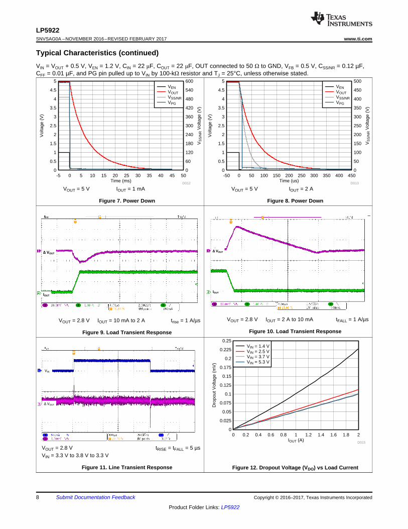
Typical Characteristics (continued)VIN = VOUT + 0.5 V, VEN = 1.2 V, CIN = 22 μF, COUT = 22 μF, OUT connected to 50 Ω to GND, VFB = 0.5 V, CSS/NR = 0.12 µF,CFF = 0.01 µF, and PG pin pulled up to VIN by 100-kΩ resistor and TJ = 25°C, unless otherwise stated.
VOUT = 5 V IOUT = 1 mA
Figure 7. Power Down
VOUT = 5 V IOUT = 2 A
Figure 8. Power Down
VOUT = 2.8 V IOUT = 10 mA to 2 A trise = 1 A/µs
Figure 9. Load Transient Response
VOUT = 2.8 V IOUT = 2 A to 10 mA tFALL = 1 A/µs
Figure 10. Load Transient Response
VOUT = 2.8 V tRISE = tFALL = 5 µsVIN = 3.3 V to 3.8 V to 3.3 V
Figure 11. Line Transient Response Figure 12. Dropout Voltage (VDO) vs Load Current
Frequency (Hz)
PS
RR
(dB
)
10 20 100 1000 10000 100000 1000000 1E+7-100
-80
-60
-40
-20
0
D014
IOUT = 1 mAIOUT = 1 AIOUT = 2 A
Frequency (Hz)
Noi
se (P
V/
Hz)
10 20 50 100 1000 10000 100000 10000000.01
0.020.030.05
0.1
0.20.30.5
1
235
10
D016
IOUT = 0 AIOUT= 0.1 AIOUT = 0.5 AIOUT = 2 A
9
LP5922www.ti.com SNVSAG0A –NOVEMBER 2016–REVISED FEBRUARY 2017
Product Folder Links: LP5922
Submit Documentation FeedbackCopyright © 2016–2017, Texas Instruments Incorporated
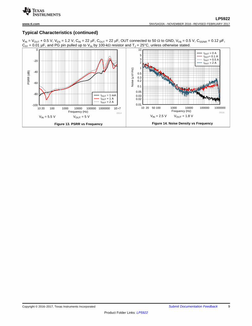
Typical Characteristics (continued)VIN = VOUT + 0.5 V, VEN = 1.2 V, CIN = 22 μF, COUT = 22 μF, OUT connected to 50 Ω to GND, VFB = 0.5 V, CSS/NR = 0.12 µF,CFF = 0.01 µF, and PG pin pulled up to VIN by 100-kΩ resistor and TJ = 25°C, unless otherwise stated.
VIN = 5.5 V VOUT = 5 V
Figure 13. PSRR vs Frequency
VIN = 2.5 V VOUT = 1.8 V
Figure 14. Noise Density vs Frequency
OUT FB LOWERUPPER
FB
(V V ) RR
V
u
Copyright © 2016, Texas Instruments Incorporated
EAVSS
AVDD
98%
VSSVREF
VFB
Reference0.5 V
IN
OUT
VREF
IN
OUT
FB
PG
SS/NRGND
EN
VIN VOUTCurrent Limit
GND
RAD
VEN
2 0
RF
CF
ULVOEnable
10
LP5922SNVSAG0A –NOVEMBER 2016–REVISED FEBRUARY 2017 www.ti.com
Product Folder Links: LP5922
Submit Documentation Feedback Copyright © 2016–2017, Texas Instruments Incorporated
7 Detailed Description
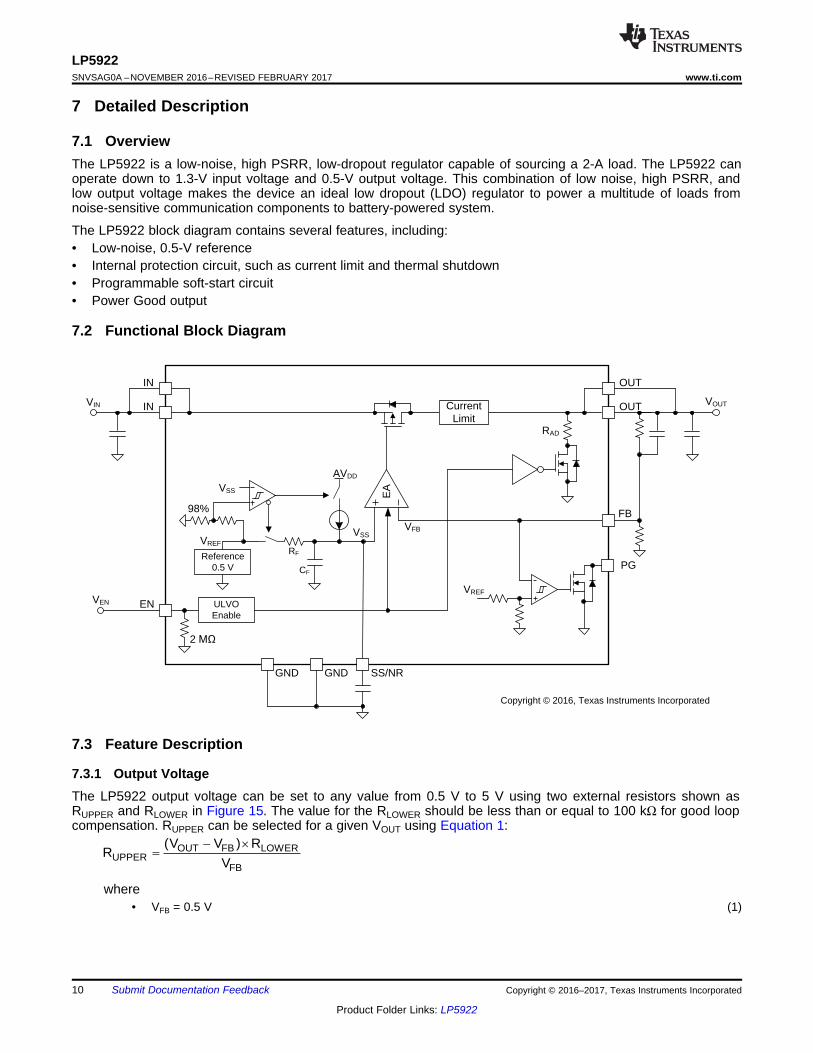
7.1 OverviewThe LP5922 is a low-noise, high PSRR, low-dropout regulator capable of sourcing a 2-A load. The LP5922 canoperate down to 1.3-V input voltage and 0.5-V output voltage. This combination of low noise, high PSRR, andlow output voltage makes the device an ideal low dropout (LDO) regulator to power a multitude of loads fromnoise-sensitive communication components to battery-powered system.
The LP5922 block diagram contains several features, including:• Low-noise, 0.5-V reference• Internal protection circuit, such as current limit and thermal shutdown• Programmable soft-start circuit• Power Good output
7.2 Functional Block Diagram
7.3 Feature Description
7.3.1 Output VoltageThe LP5922 output voltage can be set to any value from 0.5 V to 5 V using two external resistors shown asRUPPER and RLOWER in Figure 15. The value for the RLOWER should be less than or equal to 100 kΩ for good loopcompensation. RUPPER can be selected for a given VOUT using Equation 1:
where• VFB = 0.5 V (1)
SS/NR FBSS
SS
C Vt
Iu
11
LP5922www.ti.com SNVSAG0A –NOVEMBER 2016–REVISED FEBRUARY 2017
Product Folder Links: LP5922
Submit Documentation FeedbackCopyright © 2016–2017, Texas Instruments Incorporated
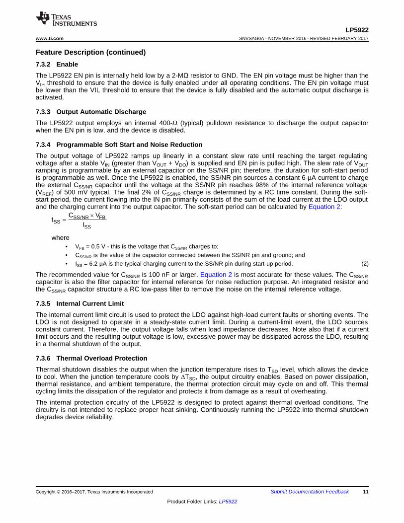
Feature Description (continued)7.3.2 EnableThe LP5922 EN pin is internally held low by a 2-MΩ resistor to GND. The EN pin voltage must be higher than theVIH threshold to ensure that the device is fully enabled under all operating conditions. The EN pin voltage mustbe lower than the VIL threshold to ensure that the device is fully disabled and the automatic output discharge isactivated.
7.3.3 Output Automatic DischargeThe LP5922 output employs an internal 400-Ω (typical) pulldown resistance to discharge the output capacitorwhen the EN pin is low, and the device is disabled.
7.3.4 Programmable Soft Start and Noise ReductionThe output voltage of LP5922 ramps up linearly in a constant slew rate until reaching the target regulatingvoltage after a stable VIN (greater than VOUT + VDO) is supplied and EN pin is pulled high. The slew rate of VOUTramping is programmable by an external capacitor on the SS/NR pin; therefore, the duration for soft-start periodis programmable as well. Once the LP5922 is enabled, the SS/NR pin sources a constant 6-µA current to chargethe external CSS/NR capacitor until the voltage at the SS/NR pin reaches 98% of the internal reference voltage(VREF) of 500 mV typical. The final 2% of CSS/NR charge is determined by a RC time constant. During the soft-start period, the current flowing into the IN pin primarily consists of the sum of the load current at the LDO outputand the charging current into the output capacitor. The soft-start period can be calculated by Equation 2:
where• VFB = 0.5 V - this is the voltage that CSS/NR charges to;• CSS/NR is the value of the capacitor connected between the SS/NR pin and ground; and• ISS = 6.2 µA is the typical charging current to the SS/NR pin during start-up period. (2)
The recommended value for CSS/NR is 100 nF or larger. Equation 2 is most accurate for these values. The CSS/NRcapacitor is also the filter capacitor for internal reference for noise reduction purpose. An integrated resistor andthe CSS/NR capacitor structure a RC low-pass filter to remove the noise on the internal reference voltage.
7.3.5 Internal Current LimitThe internal current limit circuit is used to protect the LDO against high-load current faults or shorting events. TheLDO is not designed to operate in a steady-state current limit. During a current-limit event, the LDO sourcesconstant current. Therefore, the output voltage falls when load impedance decreases. Note also that if a currentlimit occurs and the resulting output voltage is low, excessive power may be dissipated across the LDO, resultingin a thermal shutdown of the output.
7.3.6 Thermal Overload ProtectionThermal shutdown disables the output when the junction temperature rises to TSD level, which allows the deviceto cool. When the junction temperature cools by ΔTSD, the output circuitry enables. Based on power dissipation,thermal resistance, and ambient temperature, the thermal protection circuit may cycle on and off. This thermalcycling limits the dissipation of the regulator and protects it from damage as a result of overheating.
The internal protection circuitry of the LP5922 is designed to protect against thermal overload conditions. Thecircuitry is not intended to replace proper heat sinking. Continuously running the LP5922 into thermal shutdowndegrades device reliability.
12
LP5922SNVSAG0A –NOVEMBER 2016–REVISED FEBRUARY 2017 www.ti.com
Product Folder Links: LP5922
Submit Documentation Feedback Copyright © 2016–2017, Texas Instruments Incorporated
Feature Description (continued)7.3.7 Power Good OutputThe LP5922 has a Power-Good function that works by toggling the state of the PG output pin. When the outputvoltage falls below the PG threshold voltage (PGLTH), the PG pin open-drain output engages (low impedance toGND). When the output voltage rises above the PG threshold voltage (PGHTH), the PG pin becomes high-impedance. By connecting a pullup resistor to an external supply, any downstream device can receive PG as alogic signal. User must make sure that the external pullup supply voltage results in a valid logic signal for thereceiving device or devices; use a pullup resistor from 10 kΩ to 100 kΩ for best results.
In Power-Good function, the PG output pin pulled high immediatelly after output voltage rises above the PGthreshold voltage.
7.4 Device Functional Modes
7.4.1 Enable (EN)The LP5922 enable (EN) pin is internally held low by a 2-MΩ resistor to GND. If the EN pin is open the output isOFF. The EN pin voltage must be higher than the VIH threshold to ensure that the device is fully enabled underall operating conditions. When the EN pin is pulled low, and the output is disabled, the output automaticdischarge circuit is activated. Any charge on the OUT pin is discharged to GND through the internal pulldownresistance.
7.4.2 Undervoltage Lockout (UVLO)The LP5922 incorporates UVLO. The UVLO circuit monitors the input voltage and keeps the LP5922 disabledwhile a rising VIN is less than 1.2 V (typical). The rising UVLO threshold is approximately 100 mV below therecommended minimum operating VIN of 1.3 V.
7.4.3 Minimum Operating Input VoltageThe LP5922 internal circuit is not fully functional until VIN is at least 1.3 V. The output voltage is not regulateduntil VIN has reached at least the greater of 1.3 V or (VOUT + VDO).
OUT
PG
VIN
1.3 V ± 6 V
CIN COUT
EN
LP5922
VOUT
0.5 V ± 5 VIN
FPGA
VIN
GND
RUPPER
RLOWER
FB
CSS/NR
SS/NR
22 µF22 µFIN OUT
CFF
100 k
VIN
Copyright © 2016, Texas Instruments Incorporated
13
LP5922www.ti.com SNVSAG0A –NOVEMBER 2016–REVISED FEBRUARY 2017
Product Folder Links: LP5922
Submit Documentation FeedbackCopyright © 2016–2017, Texas Instruments Incorporated
8 Applications and Implementation
NOTEInformation in the following applications sections is not part of the TI componentspecification, and TI does not warrant its accuracy or completeness. TI’s customers areresponsible for determining suitability of components for their purposes. Customers shouldvalidate and test their design implementation to confirm system functionality.
8.1 Application InformationThe LP5922 is designed to meet the requirements of RF and analog circuits, by providing low noise, high PSRR,low quiescent current, and low line or load transient response figures. The device offers excellent noiseperformance without the need for a noise bypass capacitor and is stable with input and output capacitors with avalue of 22 µF. The LP5922 delivers this performance in an industry-standard WSON package which, for thisdevice, is specified with an operating junction temperature (TJ) of –40°C to +125°C.
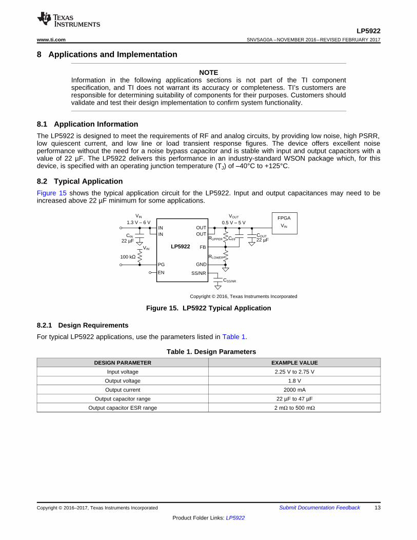
8.2 Typical ApplicationFigure 15 shows the typical application circuit for the LP5922. Input and output capacitances may need to beincreased above 22 µF minimum for some applications.
Figure 15. LP5922 Typical Application
8.2.1 Design RequirementsFor typical LP5922 applications, use the parameters listed in Table 1.
Table 1. Design ParametersDESIGN PARAMETER EXAMPLE VALUE
Input voltage 2.25 V to 2.75 VOutput voltage 1.8 VOutput current 2000 mA
Output capacitor range 22 µF to 47 µFOutput capacitor ESR range 2 mΩ to 500 mΩ
14
LP5922SNVSAG0A –NOVEMBER 2016–REVISED FEBRUARY 2017 www.ti.com
Product Folder Links: LP5922
Submit Documentation Feedback Copyright © 2016–2017, Texas Instruments Incorporated
8.2.2 Detailed Design Procedure
8.2.2.1 Custom Design With WEBENCH® ToolsClick here to create a custom design using the LP5922 device with the WEBENCH® Power Designer.1. Start by entering the input voltage (VIN), output voltage (VOUT), and output current (IOUT) requirements.2. Optimize the design for key parameters such as efficiency, footprint, and cost using the optimizer dial.3. Compare the generated design with other possible solutions from Texas Instruments.
The WEBENCH Power Designer provides a customized schematic along with a list of materials with real-timepricing and component availability.
In most cases, these actions are available:• Run electrical simulations to see important waveforms and circuit performance• Run thermal simulations to understand board thermal performance• Export customized schematic and layout into popular CAD formats• Print PDF reports for the design, and share the design with colleagues
Get more information about WEBENCH tools at www.ti.com/WEBENCH.
8.2.2.2 External CapacitorsThe LP5922 is designed to be stable using low equivalent series resistance (ESR) ceramic capacitors at theinput, output, and the noise-reduction pin (SS/NR). Multilayer ceramic capacitors have become the industrystandard for these types of applications and are recommended, but must be used with good judgment. Ceramiccapacitors that employ X7R-, X5R-, and COG-rated dielectric materials provide relatively good capacitive stabilityacross temperature, whereas the use of Y5V-rated capacitors is discouraged because of large variations incapacitance. Additionally, the case size has a direct impact on the capacitance versus applied voltage derating.
Regardless of the ceramic capacitor type selected, the actual capacitance varies with the applied operatingvoltage and temperature. As a rule of thumb, derate ceramic capacitors by at least 50%. The input and outputcapacitors recommended herein account for a effective capacitance derating of approximately 50%, but at highapplied voltage conditions the capacitance derating can be greater than 50% and must be taken intoconsideration. The minimum capacitance values declared in Input and Output Capacitors must be met across theentire expected operating voltage range and temperature range.
8.2.2.3 Input Capacitor, CIN
An input capacitor is required for stability. A capacitor with a value of at least 22 μF must be connected betweenthe LP5922 IN pin and ground for stable operation over full load current range. It is acceptable to have moreoutput capacitance than input, as long as the input is at least 22 μF.
The input capacitor must be located as close as possible to, but at a distance not more than 1 cm from, the INpin and returned to the device GND pin with a clean analog ground. This will minimize the trace inductancebetween the capacitor and the device. Any good quality ceramic or tantalum capacitor may be used at the input.
8.2.2.4 Output Capacitor, COUT
The LP5922 is designed to work specifically with a low ESR ceramic (MLCC) output capacitor, typically 22 μF. Aceramic capacitor (dielectric types X5R or X7R) in the 22-μF to 100-μF range, with an ESR not exceeding 500mΩ, is suitable in the LP5922 application circuit having an output voltage greater than 0.8 V. For output voltagesof 0.8 V or less, the output capacitance must be increased to typically 47 μF. The output capacitor must beconnected between the device OUT and GND pins. The output capacitor must meet the requirement for theminimum value of capacitance and have an ESR value that does not exceed 500 mΩ to ensure stability.
It is possible to use tantalum capacitors at the device output, but these are not as attractive for reasons of size,cost, and performance.
15
LP5922www.ti.com SNVSAG0A –NOVEMBER 2016–REVISED FEBRUARY 2017
Product Folder Links: LP5922
Submit Documentation FeedbackCopyright © 2016–2017, Texas Instruments Incorporated
A combination of multiple output capacitors in parallel boosts the high-frequency PSRR. The combination of one0805-sized, 47-µF ceramic capacitor in parallel with two 0805-sized, 10-µF ceramic capacitors with a sufficientvoltage rating optimizes PSRR response in the frequency range of 400 kHz to 700 kHz (which is a typical rangefor dc-dc supply switching frequency). This 47-µF || 10-µF || 10-µF combination also ensures that at high inputvoltage and high output voltage configurations, the minimum effective capacitance is met. Many 0805-sized, 47-µF ceramic capacitors have a voltage derating of approximately 60% to 75% at 5 V, so the addition of the two10-µF capacitors ensures that the capacitance is at or above 22 µF.
8.2.2.5 Soft-Start and Noise-Reduction Capacitor, CSS/NR
Recommended value for CSS/NR is 100 nF or larger. The soft-start period can be calculated by Equation 2. TheCSS/NR capacitor is also the filter capacitor for internal reference for noise reduction purpose.
8.2.2.6 Feed-Forward Capacitor, CFF
Although a feed-forward capacitor (CFF) from the FB pin to the OUT pin is not required to achieve stability, a 10-nF external CFF optimizes the transient, noise, and PSRR performance. A higher capacitance CFF value can beused; however, the start-up time may be longer and the Power-Good signal may incorrectly indicate that theoutput voltage is settled. The maximum recommended value is 100 nF
To ensure proper PGx functionality, the time constant defined by CNR/SSx must be greater than or equal to thetime constant from CFFx. For a detailed description, see the application report Pros and Cons of Using a Feed-Forward Capacitor with a Low Dropout Regulator (SBVA042).
8.2.2.7 No-Load StabilityThe LP5922 remains stable, and in regulation, with no external load.
8.2.2.8 Power DissipationKnowing the device power dissipation and proper sizing of the thermal plane connected to the exposed thermalpad is critical to ensuring reliable operation. Device power dissipation depends on input voltage, output voltage,and load conditions and can be calculated with Equation 3.
PD(MAX) = (VIN(MAX) – VOUT) × IOUT (3)
Power dissipation can be minimized, and greater efficiency can be achieved, by using the lowest availablevoltage drop option that is greater than the dropout voltage (VDO). However, keep in mind that higher voltagedrops result in better dynamic (that is, PSRR and transient) performance.
On the WSON (DSC) package, the primary conduction path for heat is through the exposed thermal pad into thePCB. To ensure the device does not overheat, connect the exposed thermal pad, through multiple thermal vias,to an internal ground plane with an appropriate amount of PCB copper area.
Power dissipation and junction temperature are most often related by the junction-to-ambient thermal resistance(RθJA) of the combined PCB and device package and the temperature of the ambient air (TA), according toEquation 4 or Equation 5:
TJ(MAX) = TA(MAX) + (RθJA × PD(MAX)) (4)PD = (TJ(MAX) – TA(MAX)) / RθJA (5)
If the VIN – VOUT voltage is known, the maximum allowable output current can be calculated with Equation 6IOUT(MAX) = (((125°C – TA) / RθJA) / (VIN – VOUT)) (6)
Unfortunately, the RθJA value is highly dependent on the heat-spreading capability of the particular PCB design,and therefore varies according to the PCB size, total copper area, copper weight, any thermal vias, and locationof the planes. The RθJA recorded in Thermal Information is determined by the specific EIA/JEDEC JESD51-7standard for PCB and copper spreading area, and is to be used only as a relative measure of package thermalperformance. For a well designed thermal layout, RθJA is actually the sum of the package junction-to-case(bottom) thermal resistance (RθJC(bot)) plus the thermal resistance contribution by the PCB copper area acting asa heat sink.
16
LP5922SNVSAG0A –NOVEMBER 2016–REVISED FEBRUARY 2017 www.ti.com
Product Folder Links: LP5922
Submit Documentation Feedback Copyright © 2016–2017, Texas Instruments Incorporated
8.2.2.9 Estimating Junction TemperatureThe JEDEC standard now recommends the use of psi (Ψ) thermal metrics to estimate the junction temperaturesof the LDO when in-circuit on a typical PCB board application. These metrics are not strictly speaking thermalresistances, but rather offer practical and relative means of estimating junction temperatures. These psi metricsare determined to be significantly independent of the copper-spreading area. The key thermal metrics (ΨJT andΨJB) are given in the Thermal Information table and are used in accordance with Equation 7 and Equation 8.
TJ(MAX) = TTOP + (ΨJT × PD(MAX))
where• TTOP is the temperature measured at the center-top of the device package.• PD(MAX) is described at Equation 3 (7)
TJ(MAX) = TBOARD + (ΨJB × PD(MAX))
where• TBOARD is the PCB surface temperature measured 1 mm from the device package and centered on the
package edge.• PD(MAX) is described at Equation 3 (8)
For more information about the thermal characteristics ΨJT and ΨJB, see Semiconductor and IC Package ThermalMetrics ; for more information about measuring TTOP and TBOARD, see Using New Thermal Metrics ; and for moreinformation about the EIA/JEDEC JESD51 PCB used for validating RθJA, see the TI Application Report ThermalCharacteristics of Linear and Logic Packages Using JEDEC PCB Designs. These application notes are availableat www.ti.com.
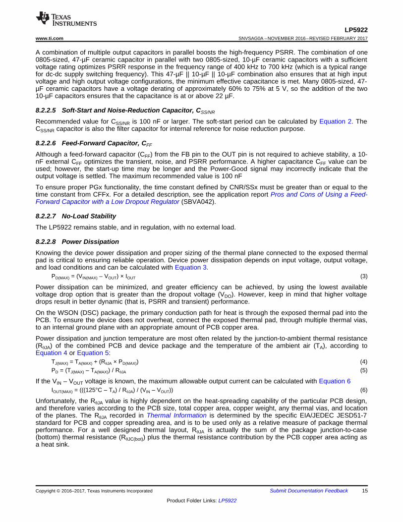
8.2.2.10 Recommended Continuous Operating AreaThe continuous operational area of an LDO is limited by the input voltage (VIN), the output voltage (VOUT), thedropout voltage (VDO), the output current (IOUT), and the junction temperature (TJ). The recommended area forcontinuous operation for a linear regulator can be separated into the following steps, and is shown in Figure 16.• Limited by dropout: Dropout voltage limits the minimum differential voltage between the input and the output
(VIN – VOUT) at a given output current level.• Limited by the rated output current: The rated output current limits the maximum recommended output current
level. Exceeding this rating causes the device to fall out of specification.• Limited by thermals: This portion of the boundary is defined by Equation 6. The slope is nonlinear because
the junction temperature of the LDO is controlled by the power dissipation (PD) across the LDO; therefore,when VIN – VOUT increases, the output current must decrease in order to ensure that the rated maximumoperating junction temperature of the device is not exceeded. Exceeding the maximum operating junctiontemperature rating can cause the device to fall out of specifications, reduces long-term reliability, and mayactivate the thermal shutdown protection circuitry.
• Limited by VIN range: The rated operating input voltage range governs both the minimum and maximum ofVIN – VOUT.
Input Voltage Output Voltage
Out
put C
urre
nt (
mA
)
0 0.5 1 1.5 2 2.5 3 3.5 4 4.5 5 5.50
200
400
600
800
1000
1200
1400
1600
1800
2000
2200
D001
TA = 25°CTA = 50°CTA = 85°CTA = 100°C
Input Voltage Output Voltage
Out
put C
urre
nt
0 0.5 1 1.5 2 2.5 3 3.5 4 4.5 50
200
400
600
800
1000
1200
1400
1600
1800
2000
2200
D002
TA = 25°CTA = 50°CTA = 85°CTA = 100°C
VIN ± VOUT (V)00
I OU
T (
A)
Limited by Minimum Operating VIN
Limited by Maximum Operating VIN
Limited by Rated Output Current
Limited by Dropout
Limited by Thermals
Recommended Area for Continuous Operation
17
LP5922www.ti.com SNVSAG0A –NOVEMBER 2016–REVISED FEBRUARY 2017
Product Folder Links: LP5922
Submit Documentation FeedbackCopyright © 2016–2017, Texas Instruments Incorporated
Figure 16. Recommended Continuous Operating Area
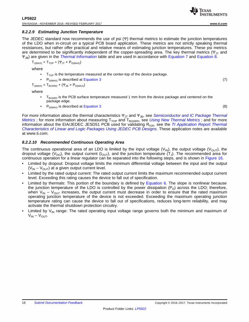
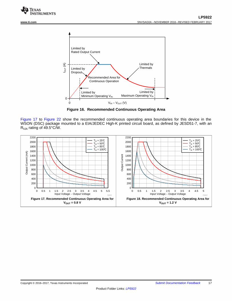
Figure 17 to Figure 22 show the recommended continuous operating area boundaries for this device in theWSON (DSC) package mounted to a EIA/JEDEC High-K printed circuit board, as defined by JESD51-7, with anRθJA rating of 49.5°C/W.
Figure 17. Recommended Continuous Operating Area forVOUT = 0.8 V
Figure 18. Recommended Continuous Operating Area forVOUT = 1.2 V
Frequency (Hz)
Noi
se (P
V/
Hz)
10 20 50 100 1000 10000 100000 10000000.01
0.020.030.05
0.1
0.20.30.5
1
235
10
D016
IOUT = 0 AIOUT= 0.1 AIOUT = 0.5 AIOUT = 2 A
IOUT (A)
I GN
D (
mA
)
0 0.2 0.4 0.6 0.8 1 1.2 1.4 1.6 1.8 20.5
0.75
1
1.25
1.5
1.75
2
2.25
2.5
2.75
3
3.25
3.5
D018
VIN = 3.3 V, VOUT = 2.8 V
Input Voltage Output Voltage
Out
put C
urre
nt (
mA
)
0.00 0.50 1.00 1.50 2.00 2.50 3.000
200
400
600
800
1000
1200
1400
1600
1800
2000
2200
D005
TA = 25°CTA = 50°CTA = 85°CTA = 100°C
Input Voltage Output Voltage (V)
Out
put C
urre
nt (
mA
)
0 0.1 0.2 0.3 0.4 0.5 0.6 0.7 0.8 0.9 1 1.1 1.20
200
400
600
800
1000
1200
1400
1600
1800
2000
2200
D006
TA = 50°CTA = 25°CTA = 85°CTA = 100°C
Input Voltage Output Voltage
Out
put C
urre
nt (
mA
)
0 0.5 1 1.5 2 2.5 3 3.5 4 4.50
200
400
600
800
1000
1200
1400
1600
1800
2000
2200
D003
TA = 25°CTA = 50°CTA = 85°CTA = 100°C
Input Voltage Output Voltage
Out
put C
urre
nt (
mA
)
0 0.5 1 1.5 2 2.5 3 3.5 40
200
400
600
800
1000
1200
1400
1600
1800
2000
2200
D004
TA = 25°CTA = 50°CTA = 85°CTA = 100°C
18
LP5922SNVSAG0A –NOVEMBER 2016–REVISED FEBRUARY 2017 www.ti.com
Product Folder Links: LP5922
Submit Documentation Feedback Copyright © 2016–2017, Texas Instruments Incorporated
Figure 19. Recommended Continuous Operating Area forVOUT = 1.8 V
Figure 20. Recommended Continuous Operating Area forVOUT = 2.5 V
Figure 21. Recommended Continuous Operating Area forVOUT = 3.3 V
Figure 22. Recommended Continuous Operating Area forVOUT = 5 V
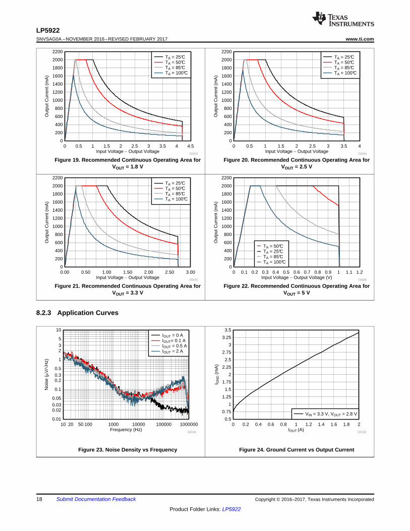
8.2.3 Application Curves
Figure 23. Noise Density vs Frequency Figure 24. Ground Current vs Output Current
OUT
GND
OUT
FB
IN
GND
SS/NR
ENPG
IN10
9
8
1
2
3
4
5
7
6
CIN
CSS/NR
COUT
RUPPER
RLOWER
RPG
GND
19
LP5922www.ti.com SNVSAG0A –NOVEMBER 2016–REVISED FEBRUARY 2017
Product Folder Links: LP5922
Submit Documentation FeedbackCopyright © 2016–2017, Texas Instruments Incorporated
9 Power Supply RecommendationsThis device is designed to operate from an input supply voltage range of 1.3 V to 6 V. The input supply should bewell regulated and free of spurious noise. To ensure that the LP5922 output voltage is well regulated anddynamic performance is optimum, the input supply must be at least VOUT + 1 V. A minimum capacitor value of22 μF is required to be within 1 cm of the IN pin.
10 Layout
10.1 Layout GuidelinesThe dynamic performance of the LP5922 is dependant on the layout of the PCB. PCB layout practices that areadequate for typical LDOs may degrade the PSRR, noise, or transient performance of the LP5922.
Best performance is achieved by placing CIN and COUT on the same side of the PCB as the LP5922 device, andas close as is practical to the package. The ground connections for CIN and COUT must be back to the LP5922GND pin using as wide and as short of a copper trace as is practical.
Avoid connections using long trace lengths, narrow trace widths, or connections through vias. These addparasitic inductances and resistance that results in inferior performance especially during transient conditions
10.2 Layout Example
Figure 25. LP5922 Typical Layout
20
LP5922SNVSAG0A –NOVEMBER 2016–REVISED FEBRUARY 2017 www.ti.com
Product Folder Links: LP5922
Submit Documentation Feedback Copyright © 2016–2017, Texas Instruments Incorporated
11 Device and Documentation Support
11.1 Device Support
11.1.1 Development Support
11.1.1.1 Custom Design With WEBENCH® ToolsClick here to create a custom design using the LP5922 device with the WEBENCH® Power Designer.1. Start by entering the input voltage (VIN), output voltage (VOUT), and output current (IOUT) requirements.2. Optimize the design for key parameters such as efficiency, footprint, and cost using the optimizer dial.3. Compare the generated design with other possible solutions from Texas Instruments.
The WEBENCH Power Designer provides a customized schematic along with a list of materials with real-timepricing and component availability.
In most cases, these actions are available:• Run electrical simulations to see important waveforms and circuit performance.• Run thermal simulations to understand board thermal performance.• Export customized schematic and layout into popular CAD formats.• Print PDF reports for the design, and share the design with colleagues.
Get more information about WEBENCH tools at www.ti.com/WEBENCH.
11.2 Related DocumentationFor additional information, see the following:• Using New Thermal Metrics• Thermal Characteristics of Linear and Logic Packages Using JEDEC PCB Designs
11.3 Receiving Notification of Documentation UpdatesTo receive notification of documentation updates, navigate to the device product folder on ti.com. In the upperright corner, click on Alert me to register and receive a weekly digest of any product information that haschanged. For change details, review the revision history included in any revised document.
11.4 Community ResourcesThe following links connect to TI community resources. Linked contents are provided "AS IS" by the respectivecontributors. They do not constitute TI specifications and do not necessarily reflect TI's views; see TI's Terms ofUse.
TI E2E™ Online Community TI's Engineer-to-Engineer (E2E) Community. Created to foster collaborationamong engineers. At e2e.ti.com, you can ask questions, share knowledge, explore ideas and helpsolve problems with fellow engineers.
Design Support TI's Design Support Quickly find helpful E2E forums along with design support tools andcontact information for technical support.
11.5 TrademarksE2E is a trademark of Texas Instruments.WEBENCH is a registered trademark of Texas Instruments.All other trademarks are the property of their respective owners.
11.6 Electrostatic Discharge CautionThis integrated circuit can be damaged by ESD. Texas Instruments recommends that all integrated circuits be handled withappropriate precautions. Failure to observe proper handling and installation procedures can cause damage.
ESD damage can range from subtle performance degradation to complete device failure. Precision integrated circuits may be moresusceptible to damage because very small parametric changes could cause the device not to meet its published specifications.
21
LP5922www.ti.com SNVSAG0A –NOVEMBER 2016–REVISED FEBRUARY 2017
Product Folder Links: LP5922
Submit Documentation FeedbackCopyright © 2016–2017, Texas Instruments Incorporated
11.7 GlossarySLYZ022 — TI Glossary.
This glossary lists and explains terms, acronyms, and definitions.
12 Mechanical, Packaging, and Orderable InformationThe following pages include mechanical, packaging, and orderable information. This information is the mostcurrent data available for the designated devices. This data is subject to change without notice and revision ofthis document. For browser-based versions of this data sheet, refer to the left-hand navigation.
PACKAGE OPTION ADDENDUM
www.ti.com 15-Feb-2017
Addendum-Page 1
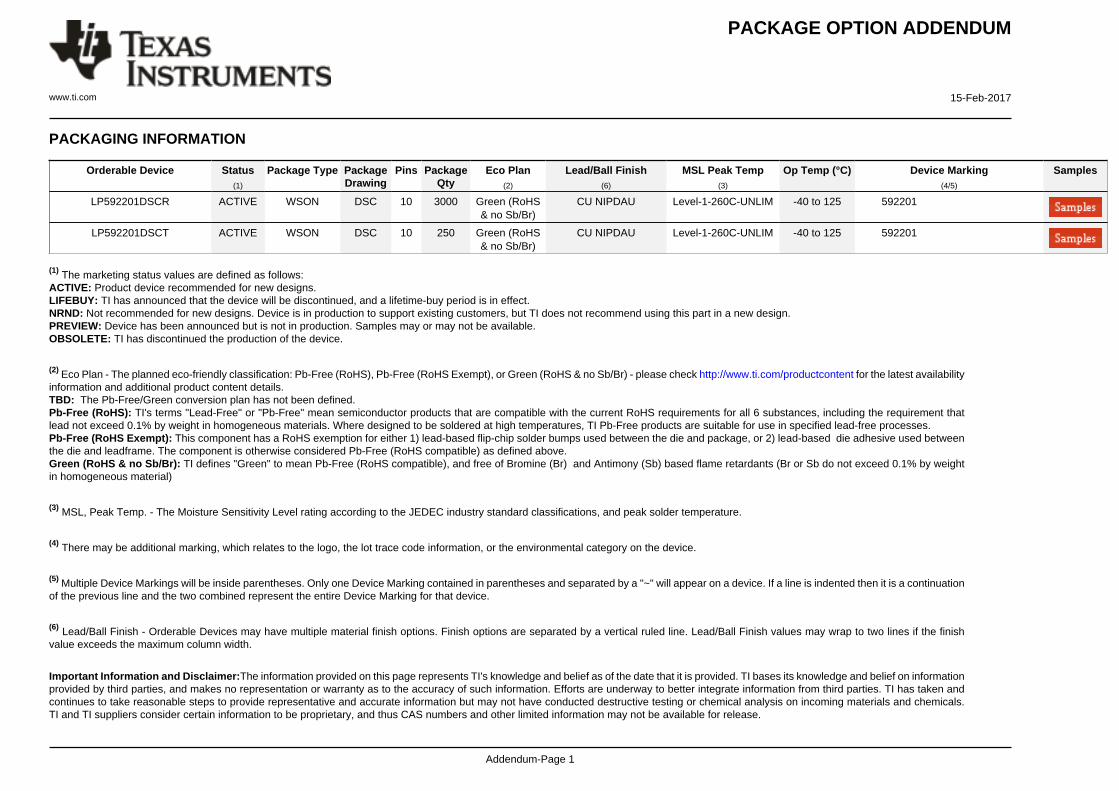
PACKAGING INFORMATION
Orderable Device Status(1)
Package Type PackageDrawing
Pins PackageQty
Eco Plan(2)
Lead/Ball Finish(6)
MSL Peak Temp(3)
Op Temp (°C) Device Marking(4/5)
Samples
LP592201DSCR ACTIVE WSON DSC 10 3000 Green (RoHS& no Sb/Br)
CU NIPDAU Level-1-260C-UNLIM -40 to 125 592201
LP592201DSCT ACTIVE WSON DSC 10 250 Green (RoHS& no Sb/Br)
CU NIPDAU Level-1-260C-UNLIM -40 to 125 592201
(1) The marketing status values are defined as follows:ACTIVE: Product device recommended for new designs.LIFEBUY: TI has announced that the device will be discontinued, and a lifetime-buy period is in effect.NRND: Not recommended for new designs. Device is in production to support existing customers, but TI does not recommend using this part in a new design.PREVIEW: Device has been announced but is not in production. Samples may or may not be available.OBSOLETE: TI has discontinued the production of the device.
(2) Eco Plan - The planned eco-friendly classification: Pb-Free (RoHS), Pb-Free (RoHS Exempt), or Green (RoHS & no Sb/Br) - please check http://www.ti.com/productcontent for the latest availabilityinformation and additional product content details.TBD: The Pb-Free/Green conversion plan has not been defined.Pb-Free (RoHS): TI's terms "Lead-Free" or "Pb-Free" mean semiconductor products that are compatible with the current RoHS requirements for all 6 substances, including the requirement thatlead not exceed 0.1% by weight in homogeneous materials. Where designed to be soldered at high temperatures, TI Pb-Free products are suitable for use in specified lead-free processes.Pb-Free (RoHS Exempt): This component has a RoHS exemption for either 1) lead-based flip-chip solder bumps used between the die and package, or 2) lead-based die adhesive used betweenthe die and leadframe. The component is otherwise considered Pb-Free (RoHS compatible) as defined above.Green (RoHS & no Sb/Br): TI defines "Green" to mean Pb-Free (RoHS compatible), and free of Bromine (Br) and Antimony (Sb) based flame retardants (Br or Sb do not exceed 0.1% by weightin homogeneous material)
(3) MSL, Peak Temp. - The Moisture Sensitivity Level rating according to the JEDEC industry standard classifications, and peak solder temperature.
(4) There may be additional marking, which relates to the logo, the lot trace code information, or the environmental category on the device.
(5) Multiple Device Markings will be inside parentheses. Only one Device Marking contained in parentheses and separated by a "~" will appear on a device. If a line is indented then it is a continuationof the previous line and the two combined represent the entire Device Marking for that device.
(6) Lead/Ball Finish - Orderable Devices may have multiple material finish options. Finish options are separated by a vertical ruled line. Lead/Ball Finish values may wrap to two lines if the finishvalue exceeds the maximum column width.
Important Information and Disclaimer:The information provided on this page represents TI's knowledge and belief as of the date that it is provided. TI bases its knowledge and belief on informationprovided by third parties, and makes no representation or warranty as to the accuracy of such information. Efforts are underway to better integrate information from third parties. TI has taken andcontinues to take reasonable steps to provide representative and accurate information but may not have conducted destructive testing or chemical analysis on incoming materials and chemicals.TI and TI suppliers consider certain information to be proprietary, and thus CAS numbers and other limited information may not be available for release.
PACKAGE OPTION ADDENDUM
www.ti.com 15-Feb-2017
Addendum-Page 2
In no event shall TI's liability arising out of such information exceed the total purchase price of the TI part(s) at issue in this document sold by TI to Customer on an annual basis.
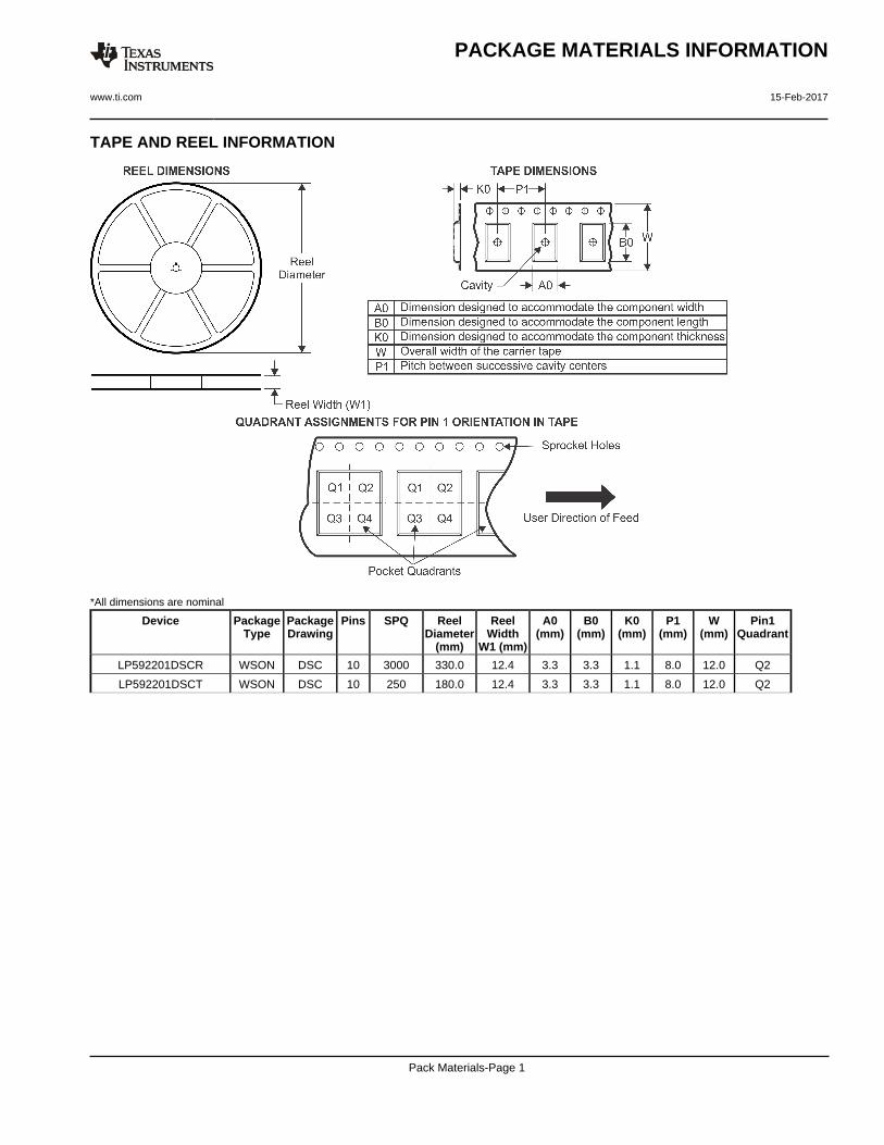
TAPE AND REEL INFORMATION
*All dimensions are nominal
Device PackageType
PackageDrawing
Pins SPQ ReelDiameter
(mm)
ReelWidth
W1 (mm)
A0(mm)
B0(mm)
K0(mm)
P1(mm)
W(mm)
Pin1Quadrant
LP592201DSCR WSON DSC 10 3000 330.0 12.4 3.3 3.3 1.1 8.0 12.0 Q2
LP592201DSCT WSON DSC 10 250 180.0 12.4 3.3 3.3 1.1 8.0 12.0 Q2
PACKAGE MATERIALS INFORMATION
www.ti.com 15-Feb-2017
Pack Materials-Page 1
*All dimensions are nominal
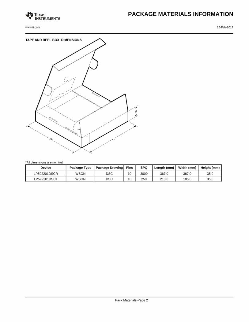
Device Package Type Package Drawing Pins SPQ Length (mm) Width (mm) Height (mm)
LP592201DSCR WSON DSC 10 3000 367.0 367.0 35.0
LP592201DSCT WSON DSC 10 250 210.0 185.0 35.0
PACKAGE MATERIALS INFORMATION
www.ti.com 15-Feb-2017
Pack Materials-Page 2
www.ti.com
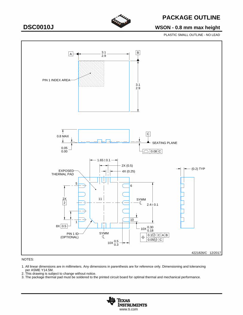
PACKAGE OUTLINE
C
10X 0.300.18
2.4 0.1
2X2
1.65 0.1
8X 0.5
10X 0.50.3
0.050.00
0.8 MAX
A 3.12.9
B
3.12.9
(0.2) TYP4X (0.25)
2X (0.5)
WSON - 0.8 mm max heightDSC0010JPLASTIC SMALL OUTLINE - NO LEAD
4221826/C 12/2017
PIN 1 INDEX AREA
SEATING PLANE
0.08 C
1
56
10
(OPTIONAL)PIN 1 ID 0.1 C A B
0.05 C
THERMAL PADEXPOSED
SYMM
SYMM11
NOTES: 1. All linear dimensions are in millimeters. Any dimensions in parenthesis are for reference only. Dimensioning and tolerancing per ASME Y14.5M. 2. This drawing is subject to change without notice. 3. The package thermal pad must be soldered to the printed circuit board for optimal thermal and mechanical performance.
SCALE 4.000
www.ti.com
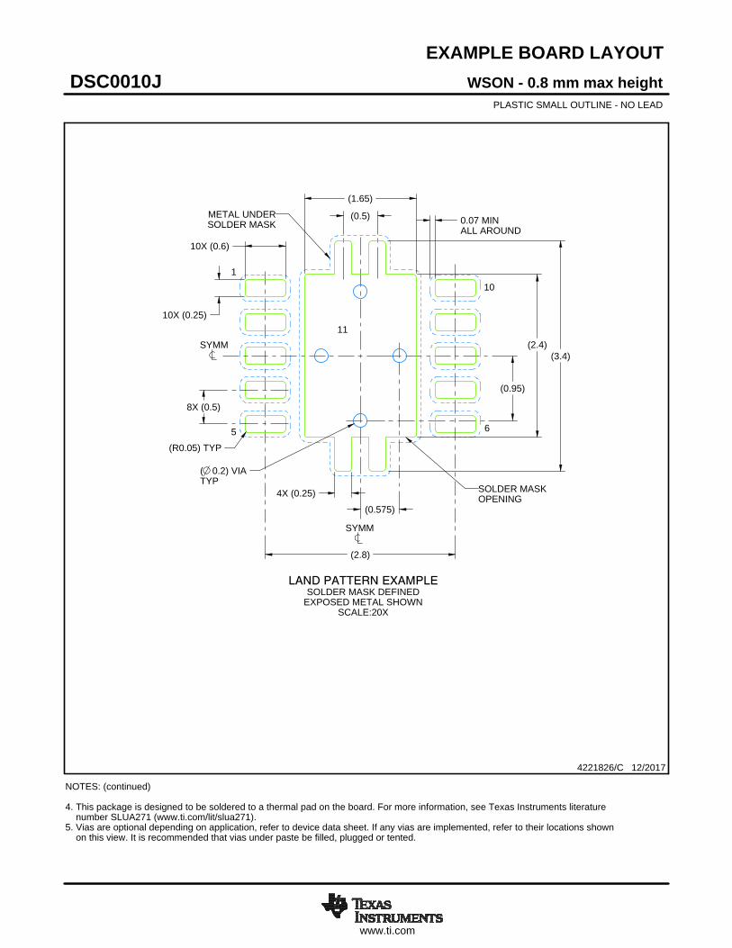
EXAMPLE BOARD LAYOUT
0.07 MINALL AROUND
10X (0.25)
(2.4)
(2.8)
8X (0.5)
(1.65)
( 0.2) VIATYP
(0.575)
(0.95)
10X (0.6)
(R0.05) TYP
(3.4)
4X (0.25)
(0.5)
WSON - 0.8 mm max heightDSC0010JPLASTIC SMALL OUTLINE - NO LEAD
4221826/C 12/2017
SYMM
1
5 6
10
LAND PATTERN EXAMPLESOLDER MASK DEFINED
EXPOSED METAL SHOWNSCALE:20X
11SYMM
METAL UNDERSOLDER MASK
SOLDER MASKOPENING
NOTES: (continued) 4. This package is designed to be soldered to a thermal pad on the board. For more information, see Texas Instruments literature number SLUA271 (www.ti.com/lit/slua271).5. Vias are optional depending on application, refer to device data sheet. If any vias are implemented, refer to their locations shown on this view. It is recommended that vias under paste be filled, plugged or tented.
www.ti.com
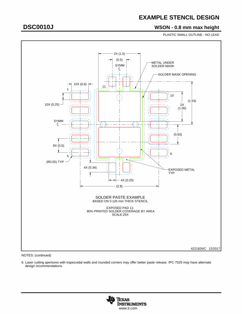
EXAMPLE STENCIL DESIGN
(R0.05) TYP
10X (0.25)
10X (0.6)
2X (1.5)
2X(1.06)
(2.8)
(0.63)
8X (0.5)
(0.5)
4X (0.34)
4X (0.25)
(1.53)
WSON - 0.8 mm max heightDSC0010JPLASTIC SMALL OUTLINE - NO LEAD
4221826/C 12/2017
NOTES: (continued) 6. Laser cutting apertures with trapezoidal walls and rounded corners may offer better paste release. IPC-7525 may have alternate design recommendations.
SOLDER PASTE EXAMPLEBASED ON 0.125 mm THICK STENCIL
EXPOSED PAD 11:
80% PRINTED SOLDER COVERAGE BY AREASCALE:25X
SYMM
1
56
10
EXPOSED METALTYP
11
SYMM
SOLDER MASK OPENING
METAL UNDERSOLDER MASK
IMPORTANT NOTICE
Texas Instruments Incorporated (TI) reserves the right to make corrections, enhancements, improvements and other changes to itssemiconductor products and services per JESD46, latest issue, and to discontinue any product or service per JESD48, latest issue. Buyersshould obtain the latest relevant information before placing orders and should verify that such information is current and complete.TI’s published terms of sale for semiconductor products (http://www.ti.com/sc/docs/stdterms.htm) apply to the sale of packaged integratedcircuit products that TI has qualified and released to market. Additional terms may apply to the use or sale of other types of TI products andservices.Reproduction of significant portions of TI information in TI data sheets is permissible only if reproduction is without alteration and isaccompanied by all associated warranties, conditions, limitations, and notices. TI is not responsible or liable for such reproduceddocumentation. Information of third parties may be subject to additional restrictions. Resale of TI products or services with statementsdifferent from or beyond the parameters stated by TI for that product or service voids all express and any implied warranties for theassociated TI product or service and is an unfair and deceptive business practice. TI is not responsible or liable for any such statements.Buyers and others who are developing systems that incorporate TI products (collectively, “Designers”) understand and agree that Designersremain responsible for using their independent analysis, evaluation and judgment in designing their applications and that Designers havefull and exclusive responsibility to assure the safety of Designers' applications and compliance of their applications (and of all TI productsused in or for Designers’ applications) with all applicable regulations, laws and other applicable requirements. Designer represents that, withrespect to their applications, Designer has all the necessary expertise to create and implement safeguards that (1) anticipate dangerousconsequences of failures, (2) monitor failures and their consequences, and (3) lessen the likelihood of failures that might cause harm andtake appropriate actions. Designer agrees that prior to using or distributing any applications that include TI products, Designer willthoroughly test such applications and the functionality of such TI products as used in such applications.TI’s provision of technical, application or other design advice, quality characterization, reliability data or other services or information,including, but not limited to, reference designs and materials relating to evaluation modules, (collectively, “TI Resources”) are intended toassist designers who are developing applications that incorporate TI products; by downloading, accessing or using TI Resources in anyway, Designer (individually or, if Designer is acting on behalf of a company, Designer’s company) agrees to use any particular TI Resourcesolely for this purpose and subject to the terms of this Notice.TI’s provision of TI Resources does not expand or otherwise alter TI’s applicable published warranties or warranty disclaimers for TIproducts, and no additional obligations or liabilities arise from TI providing such TI Resources. TI reserves the right to make corrections,enhancements, improvements and other changes to its TI Resources. TI has not conducted any testing other than that specificallydescribed in the published documentation for a particular TI Resource.Designer is authorized to use, copy and modify any individual TI Resource only in connection with the development of applications thatinclude the TI product(s) identified in such TI Resource. NO OTHER LICENSE, EXPRESS OR IMPLIED, BY ESTOPPEL OR OTHERWISETO ANY OTHER TI INTELLECTUAL PROPERTY RIGHT, AND NO LICENSE TO ANY TECHNOLOGY OR INTELLECTUAL PROPERTYRIGHT OF TI OR ANY THIRD PARTY IS GRANTED HEREIN, including but not limited to any patent right, copyright, mask work right, orother intellectual property right relating to any combination, machine, or process in which TI products or services are used. Informationregarding or referencing third-party products or services does not constitute a license to use such products or services, or a warranty orendorsement thereof. Use of TI Resources may require a license from a third party under the patents or other intellectual property of thethird party, or a license from TI under the patents or other intellectual property of TI.TI RESOURCES ARE PROVIDED “AS IS” AND WITH ALL FAULTS. TI DISCLAIMS ALL OTHER WARRANTIES ORREPRESENTATIONS, EXPRESS OR IMPLIED, REGARDING RESOURCES OR USE THEREOF, INCLUDING BUT NOT LIMITED TOACCURACY OR COMPLETENESS, TITLE, ANY EPIDEMIC FAILURE WARRANTY AND ANY IMPLIED WARRANTIES OFMERCHANTABILITY, FITNESS FOR A PARTICULAR PURPOSE, AND NON-INFRINGEMENT OF ANY THIRD PARTY INTELLECTUALPROPERTY RIGHTS. TI SHALL NOT BE LIABLE FOR AND SHALL NOT DEFEND OR INDEMNIFY DESIGNER AGAINST ANY CLAIM,INCLUDING BUT NOT LIMITED TO ANY INFRINGEMENT CLAIM THAT RELATES TO OR IS BASED ON ANY COMBINATION OFPRODUCTS EVEN IF DESCRIBED IN TI RESOURCES OR OTHERWISE. IN NO EVENT SHALL TI BE LIABLE FOR ANY ACTUAL,DIRECT, SPECIAL, COLLATERAL, INDIRECT, PUNITIVE, INCIDENTAL, CONSEQUENTIAL OR EXEMPLARY DAMAGES INCONNECTION WITH OR ARISING OUT OF TI RESOURCES OR USE THEREOF, AND REGARDLESS OF WHETHER TI HAS BEENADVISED OF THE POSSIBILITY OF SUCH DAMAGES.Unless TI has explicitly designated an individual product as meeting the requirements of a particular industry standard (e.g., ISO/TS 16949and ISO 26262), TI is not responsible for any failure to meet such industry standard requirements.Where TI specifically promotes products as facilitating functional safety or as compliant with industry functional safety standards, suchproducts are intended to help enable customers to design and create their own applications that meet applicable functional safety standardsand requirements. Using products in an application does not by itself establish any safety features in the application. Designers mustensure compliance with safety-related requirements and standards applicable to their applications. Designer may not use any TI products inlife-critical medical equipment unless authorized officers of the parties have executed a special contract specifically governing such use.Life-critical medical equipment is medical equipment where failure of such equipment would cause serious bodily injury or death (e.g., lifesupport, pacemakers, defibrillators, heart pumps, neurostimulators, and implantables). Such equipment includes, without limitation, allmedical devices identified by the U.S. Food and Drug Administration as Class III devices and equivalent classifications outside the U.S.TI may expressly designate certain products as completing a particular qualification (e.g., Q100, Military Grade, or Enhanced Product).Designers agree that it has the necessary expertise to select the product with the appropriate qualification designation for their applicationsand that proper product selection is at Designers’ own risk. Designers are solely responsible for compliance with all legal and regulatoryrequirements in connection with such selection.Designer will fully indemnify TI and its representatives against any damages, costs, losses, and/or liabilities arising out of Designer’s non-compliance with the terms and provisions of this Notice.
Mailing Address: Texas Instruments, Post Office Box 655303, Dallas, Texas 75265Copyright © 2017, Texas Instruments Incorporated