

LOW-VOLTAGEMOTOR DRIVER WITH SERIAL …akizukidenshi.com/download/ds/ti/drv8830.pdf2•...
23
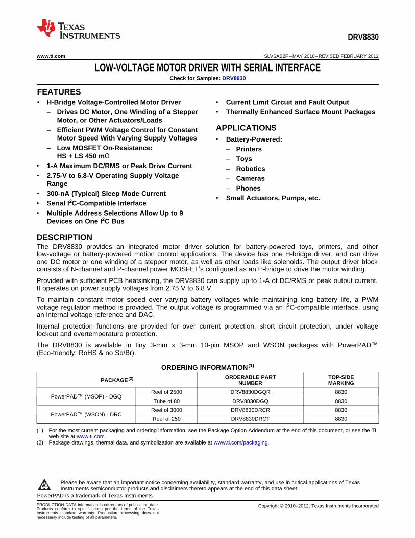
DRV8830 www.ti.com SLVSAB2F – MAY 2010 – REVISED FEBRUARY 2012 LOW-VOLTAGE MOTOR DRIVER WITH SERIAL INTERFACE Check for Samples: DRV8830 1FEATURES 2• H-Bridge Voltage-Controlled Motor Driver • Current Limit Circuit and Fault Output – Drives DC Motor, One Winding of a Stepper • Thermally Enhanced Surface Mount Packages Motor, or Other Actuators/Loads APPLICATIONS – Efficient PWM Voltage Control for Constant Motor Speed With Varying Supply Voltages • Battery-Powered: – Low MOSFET On-Resistance: – Printers HS + LS 450 mΩ – Toys • 1-A Maximum DC/RMS or Peak Drive Current – Robotics • 2.75-V to 6.8-V Operating Supply Voltage – Cameras Range – Phones • 300-nA (Typical) Sleep Mode Current • Small Actuators, Pumps, etc. • Serial I 2 C-Compatible Interface • Multiple Address Selections Allow Up to 9 Devices on One I 2 C Bus DESCRIPTION The DRV8830 provides an integrated motor driver solution for battery-powered toys, printers, and other low-voltage or battery-powered motion control applications. The device has one H-bridge driver, and can drive one DC motor or one winding of a stepper motor, as well as other loads like solenoids. The output driver block consists of N-channel and P-channel power MOSFET’s configured as an H-bridge to drive the motor winding. Provided with sufficient PCB heatsinking, the DRV8830 can supply up to 1-A of DC/RMS or peak output current. It operates on power supply voltages from 2.75 V to 6.8 V. To maintain constant motor speed over varying battery voltages while maintaining long battery life, a PWM voltage regulation method is provided. The output voltage is programmed via an I 2 C-compatible interface, using an internal voltage reference and DAC. Internal protection functions are provided for over current protection, short circuit protection, under voltage lockout and overtemperature protection. The DRV8830 is available in tiny 3-mm x 3-mm 10-pin MSOP and WSON packages with PowerPAD™ (Eco-friendly: RoHS & no Sb/Br). ORDERING INFORMATION (1) ORDERABLE PART TOP-SIDE PACKAGE (2) NUMBER MARKING Reel of 2500 DRV8830DGQR 8830 PowerPAD™ (MSOP) - DGQ Tube of 80 DRV8830DGQ 8830 Reel of 3000 DRV8830DRCR 8830 PowerPAD™ (WSON) - DRC Reel of 250 DRV8830DRCT 8830 (1) For the most current packaging and ordering information, see the Package Option Addendum at the end of this document, or see the TI web site at www.ti.com. (2) Package drawings, thermal data, and symbolization are available at www.ti.com/packaging. 1 Please be aware that an important notice concerning availability, standard warranty, and use in critical applications of Texas Instruments semiconductor products and disclaimers thereto appears at the end of this data sheet. 2PowerPAD is a trademark of Texas Instruments. PRODUCTION DATA information is current as of publication date. Copyright © 2010–2012, Texas Instruments Incorporated Products conform to specifications per the terms of the Texas Instruments standard warranty. Production processing does not necessarily include testing of all parameters.
Transcript of LOW-VOLTAGEMOTOR DRIVER WITH SERIAL …akizukidenshi.com/download/ds/ti/drv8830.pdf2•...
DRV8830
www.ti.com SLVSAB2F –MAY 2010–REVISED FEBRUARY 2012
LOW-VOLTAGE MOTOR DRIVER WITH SERIAL INTERFACECheck for Samples: DRV8830
1FEATURES2• H-Bridge Voltage-Controlled Motor Driver • Current Limit Circuit and Fault Output
– Drives DC Motor, One Winding of a Stepper • Thermally Enhanced Surface Mount PackagesMotor, or Other Actuators/Loads
APPLICATIONS– Efficient PWM Voltage Control for ConstantMotor Speed With Varying Supply Voltages • Battery-Powered:
– Low MOSFET On-Resistance: – PrintersHS + LS 450 mΩ – Toys
• 1-A Maximum DC/RMS or Peak Drive Current – Robotics• 2.75-V to 6.8-V Operating Supply Voltage – Cameras
Range – Phones• 300-nA (Typical) Sleep Mode Current • Small Actuators, Pumps, etc.• Serial I2C-Compatible Interface• Multiple Address Selections Allow Up to 9
Devices on One I2C Bus
DESCRIPTIONThe DRV8830 provides an integrated motor driver solution for battery-powered toys, printers, and otherlow-voltage or battery-powered motion control applications. The device has one H-bridge driver, and can driveone DC motor or one winding of a stepper motor, as well as other loads like solenoids. The output driver blockconsists of N-channel and P-channel power MOSFET’s configured as an H-bridge to drive the motor winding.
Provided with sufficient PCB heatsinking, the DRV8830 can supply up to 1-A of DC/RMS or peak output current.It operates on power supply voltages from 2.75 V to 6.8 V.
To maintain constant motor speed over varying battery voltages while maintaining long battery life, a PWMvoltage regulation method is provided. The output voltage is programmed via an I2C-compatible interface, usingan internal voltage reference and DAC.
Internal protection functions are provided for over current protection, short circuit protection, under voltagelockout and overtemperature protection.
The DRV8830 is available in tiny 3-mm x 3-mm 10-pin MSOP and WSON packages with PowerPAD™(Eco-friendly: RoHS & no Sb/Br).
ORDERING INFORMATION (1)
ORDERABLE PART TOP-SIDEPACKAGE (2)NUMBER MARKING
Reel of 2500 DRV8830DGQR 8830PowerPAD™ (MSOP) - DGQ
Tube of 80 DRV8830DGQ 8830
Reel of 3000 DRV8830DRCR 8830PowerPAD™ (WSON) - DRC
Reel of 250 DRV8830DRCT 8830
(1) For the most current packaging and ordering information, see the Package Option Addendum at the end of this document, or see the TIweb site at www.ti.com.
(2) Package drawings, thermal data, and symbolization are available at www.ti.com/packaging.
1
Please be aware that an important notice concerning availability, standard warranty, and use in critical applications of TexasInstruments semiconductor products and disclaimers thereto appears at the end of this data sheet.
2PowerPAD is a trademark of Texas Instruments.
PRODUCTION DATA information is current as of publication date. Copyright © 2010–2012, Texas Instruments IncorporatedProducts conform to specifications per the terms of the TexasInstruments standard warranty. Production processing does notnecessarily include testing of all parameters.
Over-
Temp
OUT1
OUT2
GND
SDA
A0
A1
VCC
VCC
VCC
Battery
DCM
Gate
Drive
Integ.
Comp
+
-
Ref
Osc
OCP
VCC
Gate
Drive
OCP
SCL
Current
Sense
FAULTn
ISENSE
I2C
Addr
Sel
5
Logic
DAC
DRV8830
SLVSAB2F –MAY 2010–REVISED FEBRUARY 2012 www.ti.com
This integrated circuit can be damaged by ESD. Texas Instruments recommends that all integrated circuits be handled withappropriate precautions. Failure to observe proper handling and installation procedures can cause damage.
ESD damage can range from subtle performance degradation to complete device failure. Precision integrated circuits may be moresusceptible to damage because very small parametric changes could cause the device not to meet its published specifications.
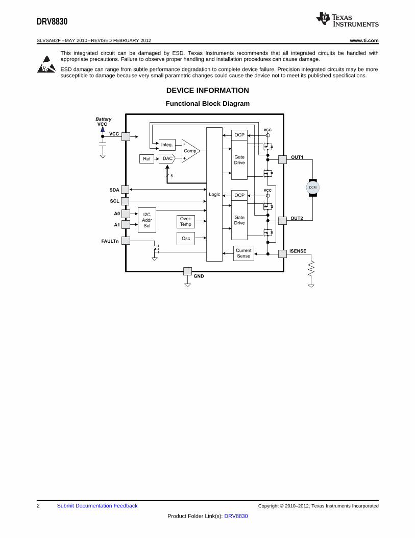
DEVICE INFORMATION
Functional Block Diagram
2 Submit Documentation Feedback Copyright © 2010–2012, Texas Instruments Incorporated
Product Folder Link(s): DRV8830
1
2
3
4
10
9
8
7
GND
(PPAD)
SCLSDAA1A0
OUT1VCC
ISENSE
OUT2
5 6 FAULTnGND
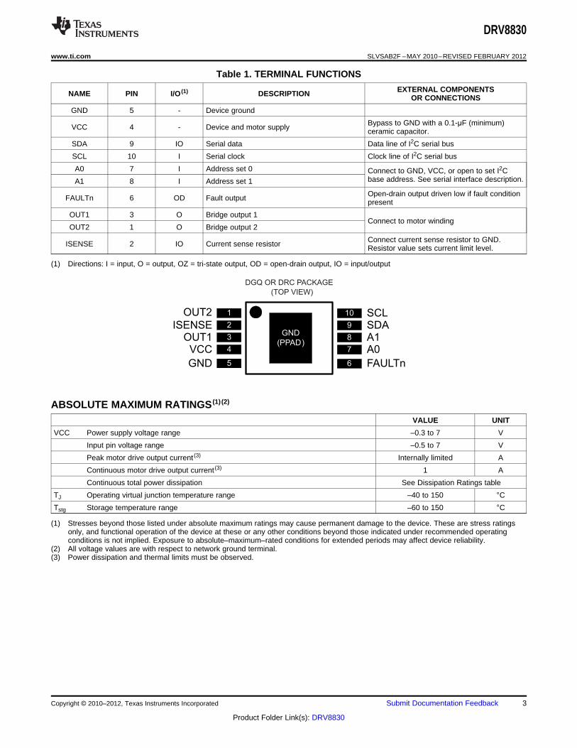
DGQ OR DRC PACKAGE
(TOP VIEW)
DRV8830
www.ti.com SLVSAB2F –MAY 2010–REVISED FEBRUARY 2012
Table 1. TERMINAL FUNCTIONS
EXTERNAL COMPONENTSNAME PIN I/O (1) DESCRIPTION OR CONNECTIONS
GND 5 - Device ground
Bypass to GND with a 0.1-μF (minimum)VCC 4 - Device and motor supply ceramic capacitor.
SDA 9 IO Serial data Data line of I2C serial bus
SCL 10 I Serial clock Clock line of I2C serial bus
A0 7 I Address set 0 Connect to GND, VCC, or open to set I2Cbase address. See serial interface description.A1 8 I Address set 1
Open-drain output driven low if fault conditionFAULTn 6 OD Fault output present
OUT1 3 O Bridge output 1Connect to motor winding
OUT2 1 O Bridge output 2
Connect current sense resistor to GND.ISENSE 2 IO Current sense resistor Resistor value sets current limit level.
(1) Directions: I = input, O = output, OZ = tri-state output, OD = open-drain output, IO = input/output
ABSOLUTE MAXIMUM RATINGS (1) (2)
VALUE UNIT
VCC Power supply voltage range –0.3 to 7 V
Input pin voltage range –0.5 to 7 V
Peak motor drive output current (3) Internally limited A
Continuous motor drive output current (3) 1 A
Continuous total power dissipation See Dissipation Ratings table
TJ Operating virtual junction temperature range –40 to 150 °CTstg Storage temperature range –60 to 150 °C
(1) Stresses beyond those listed under absolute maximum ratings may cause permanent damage to the device. These are stress ratingsonly, and functional operation of the device at these or any other conditions beyond those indicated under recommended operatingconditions is not implied. Exposure to absolute–maximum–rated conditions for extended periods may affect device reliability.
(2) All voltage values are with respect to network ground terminal.(3) Power dissipation and thermal limits must be observed.
Copyright © 2010–2012, Texas Instruments Incorporated Submit Documentation Feedback 3
Product Folder Link(s): DRV8830
DRV8830
SLVSAB2F –MAY 2010–REVISED FEBRUARY 2012 www.ti.com
THERMAL INFORMATIONDRV8830 DRV8830
THERMAL METRIC (1) DGQ DRC UNITS
10 PINS 10 PINS
θJA Junction-to-ambient thermal resistance (2) 69.3 50.2
θJCtop Junction-to-case (top) thermal resistance (3) 63.5 78.4
θJB Junction-to-board thermal resistance (4) 51.6 18.8°C/W
ψJT Junction-to-top characterization parameter (5) 1.5 1.1
ψJB Junction-to-board characterization parameter (6) 23.2 17.9
θJCbot Junction-to-case (bottom) thermal resistance (7) 9.5 5.1
(1) For more information about traditional and new thermal metrics, see the IC Package Thermal Metrics application report, SPRA953.(2) The junction-to-ambient thermal resistance under natural convection is obtained in a simulation on a JEDEC-standard, high-K board, as
specified in JESD51-7, in an environment described in JESD51-2a.(3) The junction-to-case (top) thermal resistance is obtained by simulating a cold plate test on the package top. No specific
JEDEC-standard test exists, but a close description can be found in the ANSI SEMI standard G30-88.(4) The junction-to-board thermal resistance is obtained by simulating in an environment with a ring cold plate fixture to control the PCB
temperature, as described in JESD51-8.(5) The junction-to-top characterization parameter, ψJT, estimates the junction temperature of a device in a real system and is extracted
from the simulation data for obtaining θJA, using a procedure described in JESD51-2a (sections 6 and 7).(6) The junction-to-board characterization parameter, ψJB, estimates the junction temperature of a device in a real system and is extracted
from the simulation data for obtaining θJA , using a procedure described in JESD51-2a (sections 6 and 7).(7) The junction-to-case (bottom) thermal resistance is obtained by simulating a cold plate test on the exposed (power) pad. No specific
JEDEC standard test exists, but a close description can be found in the ANSI SEMI standard G30-88.
RECOMMENDED OPERATING CONDITIONSover operating free-air temperature range (unless otherwise noted)
MIN NOM MAX UNIT
VCC Motor power supply voltage range 2.75 6.8 V
IOUT Continuous or peak H-bridge output current (1) 0 1 A
(1) Power dissipation and thermal limits must be observed.
4 Submit Documentation Feedback Copyright © 2010–2012, Texas Instruments Incorporated
Product Folder Link(s): DRV8830

DRV8830
www.ti.com SLVSAB2F –MAY 2010–REVISED FEBRUARY 2012
ELECTRICAL CHARACTERISTICSVCC = 2.75 V to 6.8 V, TA = -40°C to 85°C (unless otherwise noted)
PARAMETER TEST CONDITIONS MIN TYP MAX UNIT
POWER SUPPLIES
IVCC VCC operating supply current VCC = 5 V 1.4 2 mA
IVCCQ VCC sleep mode supply current VCC = 5 V, TA = 25°C 0.3 1 μA
VCC rising 2.575 2.75VCC undervoltage lockoutVUVLO Vvoltage VCC falling 2.47
LOGIC-LEVEL INPUTS
VIL Input low voltage 0.25 x VCC 0.38 x VCC V
VIH Input high voltage 0.46 x VCC 0.5 x VCC V
VHYS Input hysteresis 0.08 x VCC V
IIL Input low current VIN = 0 -10 10 μA
IIH Input high current VIN = 3.3 V 50 μA
LOGIC-LEVEL OUTPUTS (FAULTn)
VOL Output low voltage IOL = 4 mA, VCC = 5 V 0.5 V
H-BRIDGE FETS
VCC = 5 V, I O = 0.8 A, TJ = 85°C 290 400RDS(ON) HS FET on resistance mΩ
VCC = 5 V, I O = 0.8 A, TJ = 25°C 250
VCC = 5 V, I O = 0.8 A, TJ = 85°C 230 320RDS(ON) LS FET on resistance mΩ
VCC = 5 V, I O = 0.8 A, TJ = 25°C 200
IOFF Off-state leakage current –20 20 μA
MOTOR DRIVER
tR Rise time VCC = 3 V, load = 4 Ω 50 300 ns
tF Fall time VCC = 3 V, load = 4 Ω 50 300 ns
fSW Internal PWM frequency 44.5 kHz
PROTECTION CIRCUITS
IOCP Overcurrent protection trip level 1.3 3 A
tOCP OCP deglitch time 2 μs
TTSD Thermal shutdown temperature Die temperature (1) 150 160 180 °CVOLTAGE CONTROL
VREF Reference output voltage 1.235 1.285 1.335 V
VCC = 3.3 V to 6 V, VOUT = 3 V, (1)ΔVLINE Line regulation ±1 %IOUT = 500 mA
VCC = 5 V, VOUT = 3 V,ΔVLOAD Load regulation ±1 %IOUT = 200 mA to 800 mA (1)
CURRENT LIMIT
VILIM Current limit sense voltage 160 200 240 mV
tILIM Current limit fault deglitch time 275 ms
Current limit sense resistanceRISEN 0 1 Ω(external resistor value)
(1) Not production tested.
Copyright © 2010–2012, Texas Instruments Incorporated Submit Documentation Feedback 5
Product Folder Link(s): DRV8830
SCL
SDA0.7 VCC
0.3 VCC
0.7 VCC
0.3 VCC
1/fscl
tscl
tsch
ticf
ticf
ticr tsdh
tsdsticr
tvd
tsth
Start Condition
1 2 3 4
SCL
SDA0.7 VCC
0.3 VCC
0.7 VCC
0.3 VCC9
D7/A
tvd
tsds
tsps
tbuf
Stop Condition
Start Condition
8
DRV8830
SLVSAB2F –MAY 2010–REVISED FEBRUARY 2012 www.ti.com
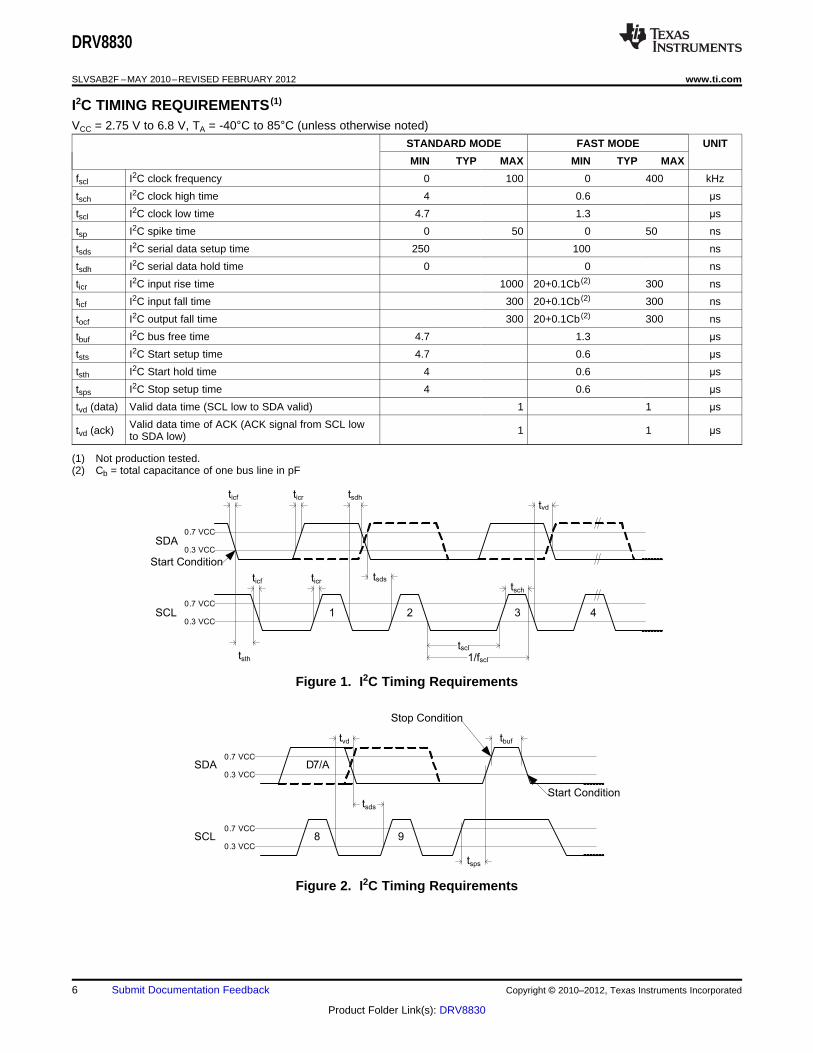
I2C TIMING REQUIREMENTS (1)
VCC = 2.75 V to 6.8 V, TA = -40°C to 85°C (unless otherwise noted)
STANDARD MODE FAST MODE UNIT
MIN TYP MAX MIN TYP MAX
fscl I2C clock frequency 0 100 0 400 kHz
tsch I2C clock high time 4 0.6 µs
tscl I2C clock low time 4.7 1.3 µs
tsp I2C spike time 0 50 0 50 ns
tsds I2C serial data setup time 250 100 ns
tsdh I2C serial data hold time 0 0 ns
ticr I2C input rise time 1000 20+0.1Cb (2) 300 ns
ticf I2C input fall time 300 20+0.1Cb (2) 300 ns
tocf I2C output fall time 300 20+0.1Cb (2) 300 ns
tbuf I2C bus free time 4.7 1.3 µs
tsts I2C Start setup time 4.7 0.6 µs
tsth I2C Start hold time 4 0.6 µs
tsps I2C Stop setup time 4 0.6 µs
tvd (data) Valid data time (SCL low to SDA valid) 1 1 µs
Valid data time of ACK (ACK signal from SCL lowtvd (ack) 1 1 µsto SDA low)
(1) Not production tested.(2) Cb = total capacitance of one bus line in pF
Figure 1. I2C Timing Requirements
Figure 2. I2C Timing Requirements
6 Submit Documentation Feedback Copyright © 2010–2012, Texas Instruments Incorporated
Product Folder Link(s): DRV8830

50%
55%
60%
65%
70%
75%
80%
85%
90%
95%
100%
0.2 0.4 0.6 0.8
LOAD - A
EF
FIC
IEN
CY
0%
10%
20%
30%
40%
50%
60%
70%
80%
90%
100%
0.5 1.5 2.5 3.5 4.5 5.5
V - VOUT
EF
FIC
EN
CY
Linear Regulator
DRV8830
DRV8830
www.ti.com SLVSAB2F –MAY 2010–REVISED FEBRUARY 2012
TYPICAL PERFORMANCE GRAPHSEFFICIENCY
vsLOAD CURRENT
(VIN = 5 V, VOUT = 3 V)
Figure 3.
EFFICIENCYvs
OUTPUT VOLTAGE(VIN = 5 V, IOUT = 500 mA)
Figure 4.
Copyright © 2010–2012, Texas Instruments Incorporated Submit Documentation Feedback 7
Product Folder Link(s): DRV8830
OUT1
OUT2
VCC
IN2 Pre-
drive
VCC
+
-
PWM
OCP
OCP
IN1
VSET
Integrator DIFF
COMP
DCM
/4
ISEN+
-COMP
REF
ITRIP
DRV8830
SLVSAB2F –MAY 2010–REVISED FEBRUARY 2012 www.ti.com
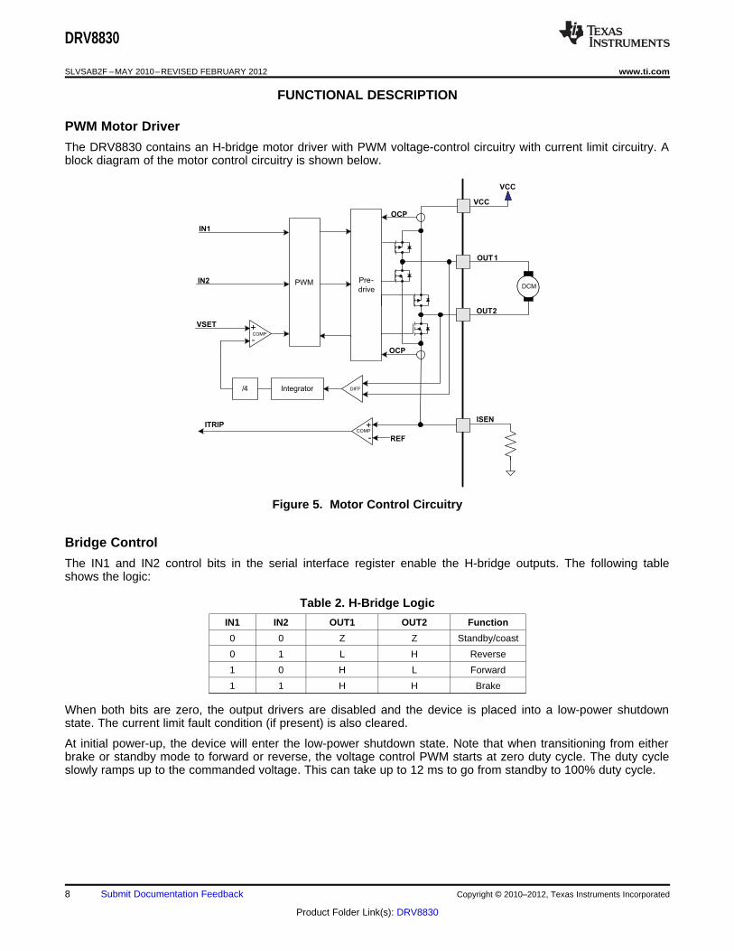
FUNCTIONAL DESCRIPTION
PWM Motor Driver
The DRV8830 contains an H-bridge motor driver with PWM voltage-control circuitry with current limit circuitry. Ablock diagram of the motor control circuitry is shown below.
Figure 5. Motor Control Circuitry
Bridge Control
The IN1 and IN2 control bits in the serial interface register enable the H-bridge outputs. The following tableshows the logic:
Table 2. H-Bridge Logic
IN1 IN2 OUT1 OUT2 Function
0 0 Z Z Standby/coast
0 1 L H Reverse
1 0 H L Forward
1 1 H H Brake
When both bits are zero, the output drivers are disabled and the device is placed into a low-power shutdownstate. The current limit fault condition (if present) is also cleared.
At initial power-up, the device will enter the low-power shutdown state. Note that when transitioning from eitherbrake or standby mode to forward or reverse, the voltage control PWM starts at zero duty cycle. The duty cycleslowly ramps up to the commanded voltage. This can take up to 12 ms to go from standby to 100% duty cycle.
8 Submit Documentation Feedback Copyright © 2010–2012, Texas Instruments Incorporated
Product Folder Link(s): DRV8830
OUT1 OUT2
2
1
2
PWM on
PWM off
VCC
1Shown with
IN1=1, IN2=0
DRV8830
www.ti.com SLVSAB2F –MAY 2010–REVISED FEBRUARY 2012
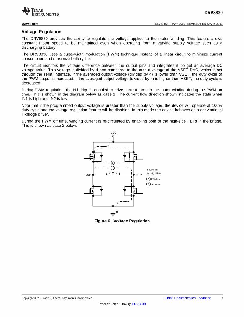
Voltage Regulation
The DRV8830 provides the ability to regulate the voltage applied to the motor winding. This feature allowsconstant motor speed to be maintained even when operating from a varying supply voltage such as adischarging battery.
The DRV8830 uses a pulse-width modulation (PWM) technique instead of a linear circuit to minimize currentconsumption and maximize battery life.
The circuit monitors the voltage difference between the output pins and integrates it, to get an average DCvoltage value. This voltage is divided by 4 and compared to the output voltage of the VSET DAC, which is setthrough the serial interface. If the averaged output voltage (divided by 4) is lower than VSET, the duty cycle ofthe PWM output is increased; if the averaged output voltage (divided by 4) is higher than VSET, the duty cycle isdecreased.
During PWM regulation, the H-bridge is enabled to drive current through the motor winding during the PWM ontime. This is shown in the diagram below as case 1. The current flow direction shown indicates the state whenIN1 is high and IN2 is low.
Note that if the programmed output voltage is greater than the supply voltage, the device will operate at 100%duty cycle and the voltage regulation feature will be disabled. In this mode the device behaves as a conventionalH-bridge driver.
During the PWM off time, winding current is re-circulated by enabling both of the high-side FETs in the bridge.This is shown as case 2 below.
Figure 6. Voltage Regulation
Copyright © 2010–2012, Texas Instruments Incorporated Submit Documentation Feedback 9
Product Folder Link(s): DRV8830
DRV8830
SLVSAB2F –MAY 2010–REVISED FEBRUARY 2012 www.ti.com
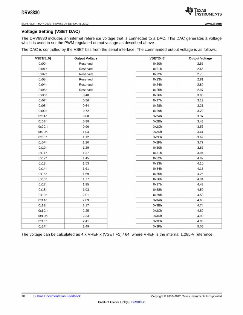
Voltage Setting (VSET DAC)
The DRV8830 includes an internal reference voltage that is connected to a DAC. This DAC generates a voltagewhich is used to set the PWM regulated output voltage as described above.
The DAC is controlled by the VSET bits from the serial interface. The commanded output voltage is as follows:
VSET[5..0] Output Voltage VSET[5..0] Output Voltage
0x00h Reserved 0x20h 2.57
0x01h Reserved 0x21h 2.65
0x02h Reserved 0x22h 2.73
0x03h Reserved 0x23h 2.81
0x04h Reserved 0x24h 2.89
0x05h Reserved 0x25h 2.97
0x06h 0.48 0x26h 3.05
0x07h 0.56 0x27h 3.13
0x08h 0.64 0x28h 3.21
0x09h 0.72 0x29h 3.29
0x0Ah 0.80 0x2Ah 3.37
0x0Bh 0.88 0x2Bh 3.45
0x0Ch 0.96 0x2Ch 3.53
0x0Dh 1.04 0x2Dh 3.61
0x0Eh 1.12 0x2Eh 3.69
0x0Fh 1.20 0x2Fh 3.77
0x10h 1.29 0x30h 3.86
0x11h 1.37 0x31h 3.94
0x12h 1.45 0x32h 4.02
0x13h 1.53 0x33h 4.10
0x14h 1.61 0x34h 4.18
0x15h 1.69 0x35h 4.26
0x16h 1.77 0x36h 4.34
0x17h 1.85 0x37h 4.42
0x18h 1.93 0x38h 4.50
0x19h 2.01 0x39h 4.58
0x1Ah 2.09 0x3Ah 4.66
0x1Bh 2.17 0x3Bh 4.74
0x1Ch 2.25 0x3Ch 4.82
0x1Dh 2.33 0x3Dh 4.90
0x1Eh 2.41 0x3Eh 4.98
0x1Fh 2.49 0x3Fh 5.06
The voltage can be calculated as 4 x VREF x (VSET +1) / 64, where VREF is the internal 1.285-V reference.
10 Submit Documentation Feedback Copyright © 2010–2012, Texas Instruments Incorporated
Product Folder Link(s): DRV8830
R =ISENSE
200 mV¾
ILIMIT
DRV8830
www.ti.com SLVSAB2F –MAY 2010–REVISED FEBRUARY 2012
Current Limit
A current limit circuit is provided to protect the system in the event of an overcurrent condition, such as whatwould be encountered if driving a DC motor at start-up or with an abnormal mechanical load (stall condition).
The motor current is sensed by monitoring the voltage across an external sense resistor. When the voltageexceeds a reference voltage of 200 mV for more than approximately 3 µs, the PWM duty cycle is reduced to limitthe current through the motor to this value. This current limit allows for starting the motor while controlling thecurrent.
If the current limit condition persists for some time, it is likely that a fault condition has been encountered, suchas the motor being run into a stop or a stalled condition. An overcurrent event must persist for approximately275 ms before the fault is registered. After approximately 275 ms, a fault signaled to the host by driving theFAULTn signal low and setting the FAULT and ILIMIT bits in the serial interface register. Operation of the motordriver will continue.
The current limit fault condition is cleared by setting both IN1 and IN2 to zero to disable the motor current, byputting the device into the shutdown state (IN1 and IN2 both set to 1), by setting the CLEAR bit in the faultregister, or by removing and re-applying power to the device.
The resistor used to set the current limit must be less than 1 Ω. Its value may be calculated as follows:
(1)
Where:
RISENSE is the current sense resistor value.
ILIMIT is the desired current limit (in mA).
If the current limit feature is not needed, the ISENSE pin may be directly connected to ground.
Protection Circuits
The DRV8830 is fully protected against undervoltage, overcurrent and overtemperature events. A FAULTn pin isavailable to signal a fault condition to the system, as well as a FAULT register in the serial interface that allowsdetermination of the fault source.
Overcurrent Protection (OCP)
An analog current limit circuit on each FET limits the current through the FET by removing the gate drive. If thisanalog current limit persists for longer than the OCP time, all FETs in the H-bridge will be disabled, the FAULTnsignal will be driven low, and the FAULT and OCP bits in the FAULT register will be set. The device will remaindisabled until the CLEAR bit in the FAULT register is written to 1, or VCC is removed and re-applied.
Overcurrent conditions are sensed independently on both high and low side devices. A short to ground, supply,or across the motor winding will all result in an overcurrent shutdown. Note that OCP is independent of thecurrent limit function, which is typically set to engage at a lower current level; the OCP function is intended toprevent damage to the device under abnormal (e.g., short-circuit) conditions.
Thermal Shutdown (TSD)
If the die temperature exceeds safe limits, all FETs in the H-bridge will be disabled, the FAULTn signal will bedriven low, and the FAULT and OTS bits in the serial interface register will be set. Once the die temperature hasfallen to a safe level operation will automatically resume.
Undervoltage Lockout (UVLO)
If at any time the voltage on the VCC pins falls below the undervoltage lockout threshold voltage, all FETs in theH-bridge will be disabled, the FAULTn signal will be driven low, and the FAULT and UVLO bits in the FAULTregister will be set. Operation will resume when VCC rises above the UVLO threshold.
Copyright © 2010–2012, Texas Instruments Incorporated Submit Documentation Feedback 11
Product Folder Link(s): DRV8830
S
1 1
0
(As) (An)
W
S
1 1
0
(As) (Dn)
R
(Dn+1)
STA
RT
Slave
Address AC
K Sub
Address AC
KS
TA
RT
Slave
Address AC
K
Data
AC
K
Data
AC
K
ST
OP
DRV8830
SLVSAB2F –MAY 2010–REVISED FEBRUARY 2012 www.ti.com
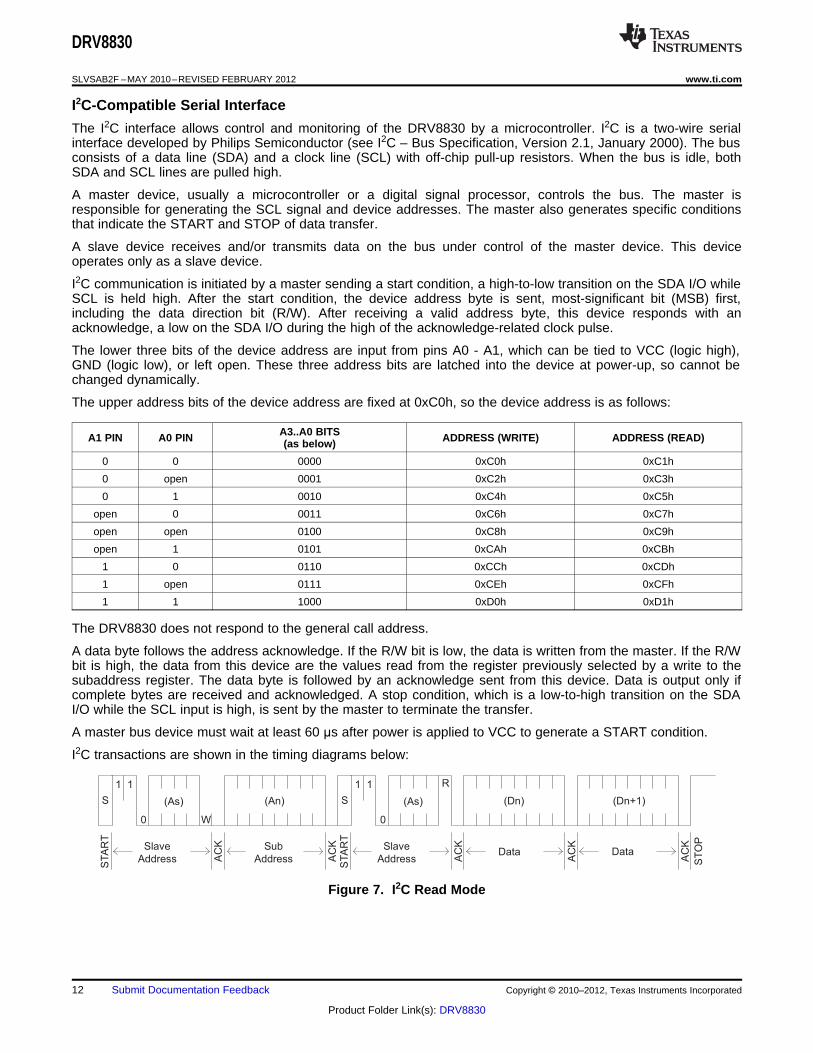
I2C-Compatible Serial Interface
The I2C interface allows control and monitoring of the DRV8830 by a microcontroller. I2C is a two-wire serialinterface developed by Philips Semiconductor (see I2C – Bus Specification, Version 2.1, January 2000). The busconsists of a data line (SDA) and a clock line (SCL) with off-chip pull-up resistors. When the bus is idle, bothSDA and SCL lines are pulled high.
A master device, usually a microcontroller or a digital signal processor, controls the bus. The master isresponsible for generating the SCL signal and device addresses. The master also generates specific conditionsthat indicate the START and STOP of data transfer.
A slave device receives and/or transmits data on the bus under control of the master device. This deviceoperates only as a slave device.
I2C communication is initiated by a master sending a start condition, a high-to-low transition on the SDA I/O whileSCL is held high. After the start condition, the device address byte is sent, most-significant bit (MSB) first,including the data direction bit (R/W). After receiving a valid address byte, this device responds with anacknowledge, a low on the SDA I/O during the high of the acknowledge-related clock pulse.
The lower three bits of the device address are input from pins A0 - A1, which can be tied to VCC (logic high),GND (logic low), or left open. These three address bits are latched into the device at power-up, so cannot bechanged dynamically.
The upper address bits of the device address are fixed at 0xC0h, so the device address is as follows:
A3..A0 BITSA1 PIN A0 PIN ADDRESS (WRITE) ADDRESS (READ)(as below)
0 0 0000 0xC0h 0xC1h
0 open 0001 0xC2h 0xC3h
0 1 0010 0xC4h 0xC5h
open 0 0011 0xC6h 0xC7h
open open 0100 0xC8h 0xC9h
open 1 0101 0xCAh 0xCBh
1 0 0110 0xCCh 0xCDh
1 open 0111 0xCEh 0xCFh
1 1 1000 0xD0h 0xD1h
The DRV8830 does not respond to the general call address.
A data byte follows the address acknowledge. If the R/W bit is low, the data is written from the master. If the R/Wbit is high, the data from this device are the values read from the register previously selected by a write to thesubaddress register. The data byte is followed by an acknowledge sent from this device. Data is output only ifcomplete bytes are received and acknowledged. A stop condition, which is a low-to-high transition on the SDAI/O while the SCL input is high, is sent by the master to terminate the transfer.
A master bus device must wait at least 60 μs after power is applied to VCC to generate a START condition.
I2C transactions are shown in the timing diagrams below:
Figure 7. I2C Read Mode
12 Submit Documentation Feedback Copyright © 2010–2012, Texas Instruments Incorporated
Product Folder Link(s): DRV8830
S
1 1
0
(As) (An)
W
STA
RT
Slave
Address AC
K Sub
Address AC
K
(Dn) (Dn+1)
Data
AC
K
Data
AC
K
ST
OP
DRV8830
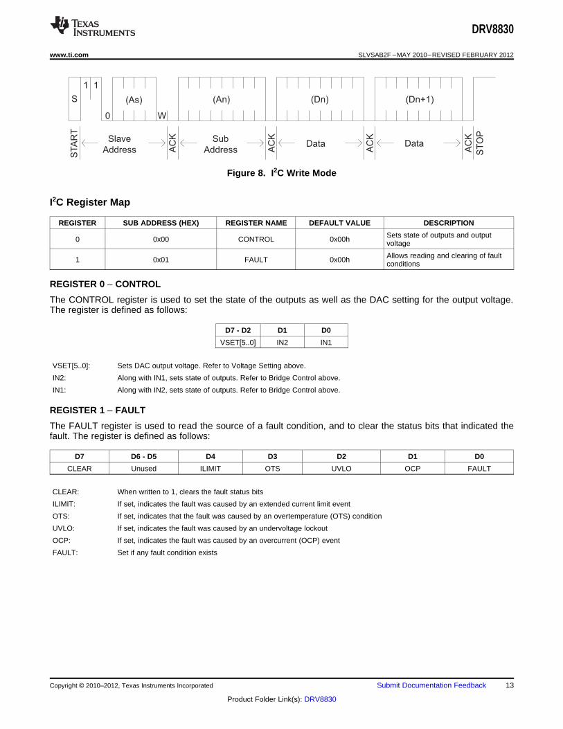
www.ti.com SLVSAB2F –MAY 2010–REVISED FEBRUARY 2012
Figure 8. I2C Write Mode
I2C Register Map
REGISTER SUB ADDRESS (HEX) REGISTER NAME DEFAULT VALUE DESCRIPTION
Sets state of outputs and output0 0x00 CONTROL 0x00h voltage
Allows reading and clearing of fault1 0x01 FAULT 0x00h conditions
REGISTER 0 – CONTROL
The CONTROL register is used to set the state of the outputs as well as the DAC setting for the output voltage.The register is defined as follows:
D7 - D2 D1 D0
VSET[5..0] IN2 IN1
VSET[5..0]: Sets DAC output voltage. Refer to Voltage Setting above.
IN2: Along with IN1, sets state of outputs. Refer to Bridge Control above.
IN1: Along with IN2, sets state of outputs. Refer to Bridge Control above.
REGISTER 1 – FAULT
The FAULT register is used to read the source of a fault condition, and to clear the status bits that indicated thefault. The register is defined as follows:
D7 D6 - D5 D4 D3 D2 D1 D0
CLEAR Unused ILIMIT OTS UVLO OCP FAULT
CLEAR: When written to 1, clears the fault status bits
ILIMIT: If set, indicates the fault was caused by an extended current limit event
OTS: If set, indicates that the fault was caused by an overtemperature (OTS) condition
UVLO: If set, indicates the fault was caused by an undervoltage lockout
OCP: If set, indicates the fault was caused by an overcurrent (OCP) event
FAULT: Set if any fault condition exists
Copyright © 2010–2012, Texas Instruments Incorporated Submit Documentation Feedback 13
Product Folder Link(s): DRV8830

P = R (I )TOT DS(ON) OUT(RMS)22
· ·
DRV8830
SLVSAB2F –MAY 2010–REVISED FEBRUARY 2012 www.ti.com
THERMAL INFORMATION
Thermal Protection
The DRV8830 has thermal shutdown (TSD) as described above. If the die temperature exceeds approximately160°C, the device will be disabled until the temperature drops to a safe level.
Any tendency of the device to enter TSD is an indication of either excessive power dissipation, insufficientheatsinking, or too high an ambient temperature.
Power Dissipation
Power dissipation in the DRV8830 is dominated by the power dissipated in the output FET resistance, or RDS(ON).Average power dissipation when running a stepper motor can be roughly estimated by Equation 2.
(2)
where PTOT is the total power dissipation, RDS(ON) is the resistance of each FET, and IOUT(RMS) is the RMS outputcurrent being applied to each winding. IOUT(RMS) is equal to the approximately 0.7x the full-scale output currentsetting. The factor of 2 comes from the fact that at any instant two FETs are conducting winding current for eachwinding (one high-side and one low-side).
The maximum amount of power that can be dissipated in the device is dependent on ambient temperature andheatsinking.
Note that RDS(ON) increases with temperature, so as the device heats, the power dissipation increases. This mustbe taken into consideration when sizing the heatsink.
14 Submit Documentation Feedback Copyright © 2010–2012, Texas Instruments Incorporated
Product Folder Link(s): DRV8830
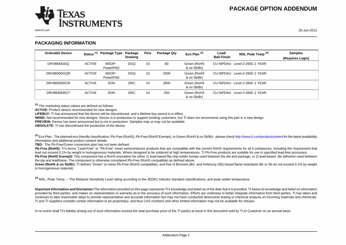
PACKAGE OPTION ADDENDUM
www.ti.com 20-Jun-2012
Addendum-Page 1
PACKAGING INFORMATION
Orderable Device Status (1) Package Type PackageDrawing
Pins Package Qty Eco Plan (2) Lead/Ball Finish
MSL Peak Temp (3) Samples
(Requires Login)
DRV8830DGQ ACTIVE MSOP-PowerPAD
DGQ 10 80 Green (RoHS& no Sb/Br)
CU NIPDAU Level-2-260C-1 YEAR
DRV8830DGQR ACTIVE MSOP-PowerPAD
DGQ 10 2500 Green (RoHS& no Sb/Br)
CU NIPDAU Level-2-260C-1 YEAR
DRV8830DRCR ACTIVE SON DRC 10 3000 Green (RoHS& no Sb/Br)
CU NIPDAU Level-2-260C-1 YEAR
DRV8830DRCT ACTIVE SON DRC 10 250 Green (RoHS& no Sb/Br)
CU NIPDAU Level-2-260C-1 YEAR
(1) The marketing status values are defined as follows:ACTIVE: Product device recommended for new designs.LIFEBUY: TI has announced that the device will be discontinued, and a lifetime-buy period is in effect.NRND: Not recommended for new designs. Device is in production to support existing customers, but TI does not recommend using this part in a new design.PREVIEW: Device has been announced but is not in production. Samples may or may not be available.OBSOLETE: TI has discontinued the production of the device.
(2) Eco Plan - The planned eco-friendly classification: Pb-Free (RoHS), Pb-Free (RoHS Exempt), or Green (RoHS & no Sb/Br) - please check http://www.ti.com/productcontent for the latest availabilityinformation and additional product content details.TBD: The Pb-Free/Green conversion plan has not been defined.Pb-Free (RoHS): TI's terms "Lead-Free" or "Pb-Free" mean semiconductor products that are compatible with the current RoHS requirements for all 6 substances, including the requirement thatlead not exceed 0.1% by weight in homogeneous materials. Where designed to be soldered at high temperatures, TI Pb-Free products are suitable for use in specified lead-free processes.Pb-Free (RoHS Exempt): This component has a RoHS exemption for either 1) lead-based flip-chip solder bumps used between the die and package, or 2) lead-based die adhesive used betweenthe die and leadframe. The component is otherwise considered Pb-Free (RoHS compatible) as defined above.Green (RoHS & no Sb/Br): TI defines "Green" to mean Pb-Free (RoHS compatible), and free of Bromine (Br) and Antimony (Sb) based flame retardants (Br or Sb do not exceed 0.1% by weightin homogeneous material)
(3) MSL, Peak Temp. -- The Moisture Sensitivity Level rating according to the JEDEC industry standard classifications, and peak solder temperature.
Important Information and Disclaimer:The information provided on this page represents TI's knowledge and belief as of the date that it is provided. TI bases its knowledge and belief on informationprovided by third parties, and makes no representation or warranty as to the accuracy of such information. Efforts are underway to better integrate information from third parties. TI has taken andcontinues to take reasonable steps to provide representative and accurate information but may not have conducted destructive testing or chemical analysis on incoming materials and chemicals.TI and TI suppliers consider certain information to be proprietary, and thus CAS numbers and other limited information may not be available for release.
In no event shall TI's liability arising out of such information exceed the total purchase price of the TI part(s) at issue in this document sold by TI to Customer on an annual basis.
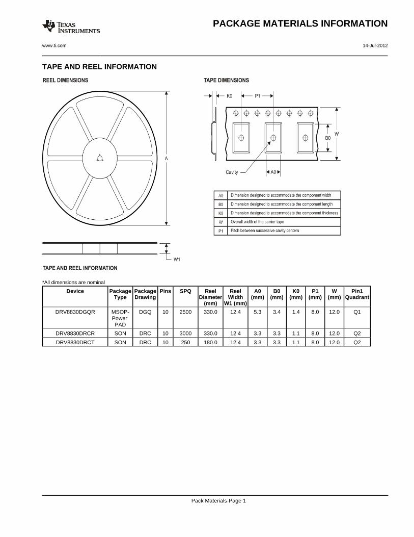
TAPE AND REEL INFORMATION
*All dimensions are nominal
Device PackageType
PackageDrawing
Pins SPQ ReelDiameter
(mm)
ReelWidth
W1 (mm)
A0(mm)
B0(mm)
K0(mm)
P1(mm)
W(mm)
Pin1Quadrant
DRV8830DGQR MSOP-Power PAD
DGQ 10 2500 330.0 12.4 5.3 3.4 1.4 8.0 12.0 Q1
DRV8830DRCR SON DRC 10 3000 330.0 12.4 3.3 3.3 1.1 8.0 12.0 Q2
DRV8830DRCT SON DRC 10 250 180.0 12.4 3.3 3.3 1.1 8.0 12.0 Q2
PACKAGE MATERIALS INFORMATION
www.ti.com 14-Jul-2012
Pack Materials-Page 1
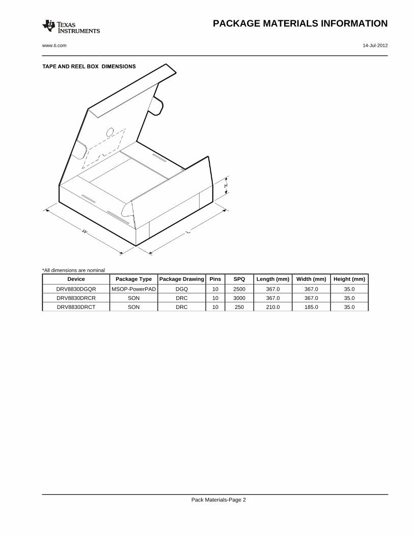
*All dimensions are nominal
Device Package Type Package Drawing Pins SPQ Length (mm) Width (mm) Height (mm)
DRV8830DGQR MSOP-PowerPAD DGQ 10 2500 367.0 367.0 35.0
DRV8830DRCR SON DRC 10 3000 367.0 367.0 35.0
DRV8830DRCT SON DRC 10 250 210.0 185.0 35.0
PACKAGE MATERIALS INFORMATION
www.ti.com 14-Jul-2012
Pack Materials-Page 2

IMPORTANT NOTICE
Texas Instruments Incorporated and its subsidiaries (TI) reserve the right to make corrections, enhancements, improvements and otherchanges to its semiconductor products and services per JESD46C and to discontinue any product or service per JESD48B. Buyers shouldobtain the latest relevant information before placing orders and should verify that such information is current and complete. Allsemiconductor products (also referred to herein as “components”) are sold subject to TI’s terms and conditions of sale supplied at the timeof order acknowledgment.
TI warrants performance of its components to the specifications applicable at the time of sale, in accordance with the warranty in TI’s termsand conditions of sale of semiconductor products. Testing and other quality control techniques are used to the extent TI deems necessaryto support this warranty. Except where mandated by applicable law, testing of all parameters of each component is not necessarilyperformed.
TI assumes no liability for applications assistance or the design of Buyers’ products. Buyers are responsible for their products andapplications using TI components. To minimize the risks associated with Buyers’ products and applications, Buyers should provideadequate design and operating safeguards.
TI does not warrant or represent that any license, either express or implied, is granted under any patent right, copyright, mask work right, orother intellectual property right relating to any combination, machine, or process in which TI components or services are used. Informationpublished by TI regarding third-party products or services does not constitute a license to use such products or services or a warranty orendorsement thereof. Use of such information may require a license from a third party under the patents or other intellectual property of thethird party, or a license from TI under the patents or other intellectual property of TI.
Reproduction of significant portions of TI information in TI data books or data sheets is permissible only if reproduction is without alterationand is accompanied by all associated warranties, conditions, limitations, and notices. TI is not responsible or liable for such altereddocumentation. Information of third parties may be subject to additional restrictions.
Resale of TI components or services with statements different from or beyond the parameters stated by TI for that component or servicevoids all express and any implied warranties for the associated TI component or service and is an unfair and deceptive business practice.TI is not responsible or liable for any such statements.
Buyer acknowledges and agrees that it is solely responsible for compliance with all legal, regulatory and safety-related requirementsconcerning its products, and any use of TI components in its applications, notwithstanding any applications-related information or supportthat may be provided by TI. Buyer represents and agrees that it has all the necessary expertise to create and implement safeguards whichanticipate dangerous consequences of failures, monitor failures and their consequences, lessen the likelihood of failures that might causeharm and take appropriate remedial actions. Buyer will fully indemnify TI and its representatives against any damages arising out of the useof any TI components in safety-critical applications.
In some cases, TI components may be promoted specifically to facilitate safety-related applications. With such components, TI’s goal is tohelp enable customers to design and create their own end-product solutions that meet applicable functional safety standards andrequirements. Nonetheless, such components are subject to these terms.
No TI components are authorized for use in FDA Class III (or similar life-critical medical equipment) unless authorized officers of the partieshave executed a special agreement specifically governing such use.
Only those TI components which TI has specifically designated as military grade or “enhanced plastic” are designed and intended for use inmilitary/aerospace applications or environments. Buyer acknowledges and agrees that any military or aerospace use of TI componentswhich have not been so designated is solely at the Buyer's risk, and that Buyer is solely responsible for compliance with all legal andregulatory requirements in connection with such use.
TI has specifically designated certain components which meet ISO/TS16949 requirements, mainly for automotive use. Components whichhave not been so designated are neither designed nor intended for automotive use; and TI will not be responsible for any failure of suchcomponents to meet such requirements.
Products Applications
Audio www.ti.com/audio Automotive and Transportation www.ti.com/automotive
Amplifiers amplifier.ti.com Communications and Telecom www.ti.com/communications
Data Converters dataconverter.ti.com Computers and Peripherals www.ti.com/computers
DLP® Products www.dlp.com Consumer Electronics www.ti.com/consumer-apps
DSP dsp.ti.com Energy and Lighting www.ti.com/energy
Clocks and Timers www.ti.com/clocks Industrial www.ti.com/industrial
Interface interface.ti.com Medical www.ti.com/medical
Logic logic.ti.com Security www.ti.com/security
Power Mgmt power.ti.com Space, Avionics and Defense www.ti.com/space-avionics-defense
Microcontrollers microcontroller.ti.com Video and Imaging www.ti.com/video
RFID www.ti-rfid.com
OMAP Mobile Processors www.ti.com/omap TI E2E Community e2e.ti.com
Wireless Connectivity www.ti.com/wirelessconnectivity
Mailing Address: Texas Instruments, Post Office Box 655303, Dallas, Texas 75265Copyright © 2012, Texas Instruments Incorporated


![Driver behaviour at roadworks - SIAS behaviour in roadworks [Published Article].pdf2. Study of driver behaviour at roadworks 2.1. Arkleston Bridge Strengthening Works Like many cities](https://static.fdocuments.in/doc/165x107/5edbda67ad6a402d6666448d/driver-behaviour-at-roadworks-behaviour-in-roadworks-published-articlepdf-2.jpg)


