
Low Temperature poly-Si TFTs for Mobile Display Applications · D. P. Gosain Proc. of ASID ’06,...
6
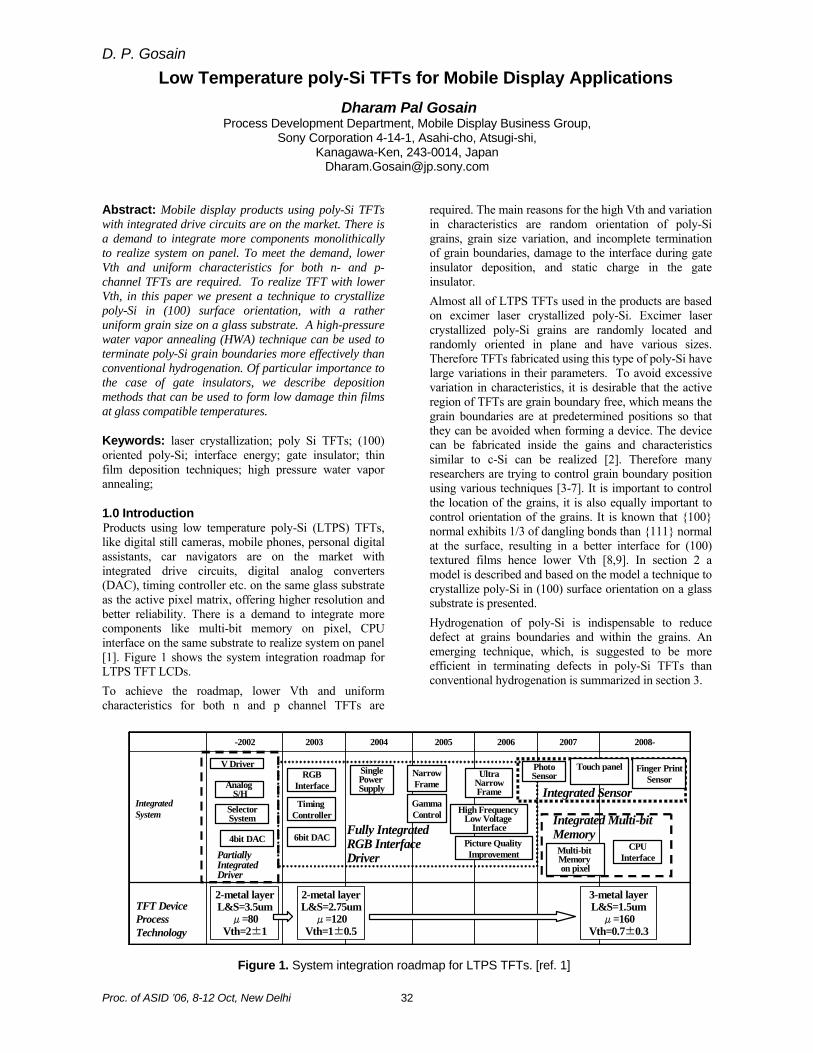
D. P. Gosain Proc. of ASID ’06, 8-12 Oct, New Delhi 32 Low Temperature poly-Si TFTs for Mobile Display Applications Dharam Pal Gosain Process Development Department, Mobile Display Business Group, Sony Corporation 4-14-1, Asahi-cho, Atsugi-shi, Kanagawa-Ken, 243-0014, Japan [email protected] Abstract: Mobile display products using poly-Si TFTs with integrated drive circuits are on the market. There is a demand to integrate more components monolithically to realize system on panel. To meet the demand, lower Vth and uniform characteristics for both n- and p- channel TFTs are required. To realize TFT with lower Vth, in this paper we present a technique to crystallize poly-Si in (100) surface orientation, with a rather uniform grain size on a glass substrate. A high-pressure water vapor annealing (HWA) technique can be used to terminate poly-Si grain boundaries more effectively than conventional hydrogenation. Of particular importance to the case of gate insulators, we describe deposition methods that can be used to form low damage thin films at glass compatible temperatures. Keywords: laser crystallization; poly Si TFTs; (100) oriented poly-Si; interface energy; gate insulator; thin film deposition techniques; high pressure water vapor annealing; 1.0 Introduction Products using low temperature poly-Si (LTPS) TFTs, like digital still cameras, mobile phones, personal digital assistants, car navigators are on the market with integrated drive circuits, digital analog converters (DAC), timing controller etc. on the same glass substrate as the active pixel matrix, offering higher resolution and better reliability. There is a demand to integrate more components like multi-bit memory on pixel, CPU interface on the same substrate to realize system on panel [1]. Figure 1 shows the system integration roadmap for LTPS TFT LCDs. To achieve the roadmap, lower Vth and uniform characteristics for both n and p channel TFTs are required. The main reasons for the high Vth and variation in characteristics are random orientation of poly-Si grains, grain size variation, and incomplete termination of grain boundaries, damage to the interface during gate insulator deposition, and static charge in the gate insulator. Almost all of LTPS TFTs used in the products are based on excimer laser crystallized poly-Si. Excimer laser crystallized poly-Si grains are randomly located and randomly oriented in plane and have various sizes. Therefore TFTs fabricated using this type of poly-Si have large variations in their parameters. To avoid excessive variation in characteristics, it is desirable that the active region of TFTs are grain boundary free, which means the grain boundaries are at predetermined positions so that they can be avoided when forming a device. The device can be fabricated inside the gains and characteristics similar to c-Si can be realized [2]. Therefore many researchers are trying to control grain boundary position using various techniques [3-7]. It is important to control the location of the grains, it is also equally important to control orientation of the grains. It is known that {100} normal exhibits 1/3 of dangling bonds than {111} normal at the surface, resulting in a better interface for (100) textured films hence lower Vth [8,9]. In section 2 a model is described and based on the model a technique to crystallize poly-Si in (100) surface orientation on a glass substrate is presented. Hydrogenation of poly-Si is indispensable to reduce defect at grains boundaries and within the grains. An emerging technique, which, is suggested to be more efficient in terminating defects in poly-Si TFTs than conventional hydrogenation is summarized in section 3. Fully Integrated RGB Interface Integrated Multi-bit Integrated Sensor 2006 2007 2008- -2002 2003 2004 2005 Integrated System Fully Integrated RGB Interface Driver Integrated Multi-bit Memory Integrated Sensor TFT Device Process Technology 2-metal layer L&S=3.5um μ=80 Vth=2±1 2-metal layer L&S=2.75um μ=120 Vth=1±0.5 3-metal layer L&S=1.5um μ=160 Vth=0.7±0.3 Partially Integrated Driver V Driver Analog S/H Selector System 4bit DAC RGB Interface Timing Controller 6bit DAC Single Power Supply Narrow Frame Gamma Control Ultra Narrow Frame High Frequency Low Voltage Interface Picture Quality Improvement Photo Sensor Touch panel Finger Print Sensor Multi-bit Memory on pixel CPU Interface Figure 1. System integration roadmap for LTPS TFTs. [ref. 1]
Transcript of Low Temperature poly-Si TFTs for Mobile Display Applications · D. P. Gosain Proc. of ASID ’06,...
D. P. Gosain
Proc. of ASID ’06, 8-12 Oct, New Delhi
32
Low Temperature poly-Si TFTs for Mobile Display Applications Dharam Pal Gosain
Process Development Department, Mobile Display Business Group, Sony Corporation 4-14-1, Asahi-cho, Atsugi-shi,
Kanagawa-Ken, 243-0014, Japan [email protected]
Abstract: Mobile display products using poly-Si TFTs with integrated drive circuits are on the market. There is a demand to integrate more components monolithically to realize system on panel. To meet the demand, lower Vth and uniform characteristics for both n- and p-channel TFTs are required. To realize TFT with lower Vth, in this paper we present a technique to crystallize poly-Si in (100) surface orientation, with a rather uniform grain size on a glass substrate. A high-pressure water vapor annealing (HWA) technique can be used to terminate poly-Si grain boundaries more effectively than conventional hydrogenation. Of particular importance to the case of gate insulators, we describe deposition methods that can be used to form low damage thin films at glass compatible temperatures.
Keywords: laser crystallization; poly Si TFTs; (100) oriented poly-Si; interface energy; gate insulator; thin film deposition techniques; high pressure water vapor annealing;
1.0 Introduction Products using low temperature poly-Si (LTPS) TFTs, like digital still cameras, mobile phones, personal digital assistants, car navigators are on the market with integrated drive circuits, digital analog converters (DAC), timing controller etc. on the same glass substrate as the active pixel matrix, offering higher resolution and better reliability. There is a demand to integrate more components like multi-bit memory on pixel, CPU interface on the same substrate to realize system on panel [1]. Figure 1 shows the system integration roadmap for LTPS TFT LCDs. To achieve the roadmap, lower Vth and uniform characteristics for both n and p channel TFTs are
required. The main reasons for the high Vth and variation in characteristics are random orientation of poly-Si grains, grain size variation, and incomplete termination of grain boundaries, damage to the interface during gate insulator deposition, and static charge in the gate insulator. Almost all of LTPS TFTs used in the products are based on excimer laser crystallized poly-Si. Excimer laser crystallized poly-Si grains are randomly located and randomly oriented in plane and have various sizes. Therefore TFTs fabricated using this type of poly-Si have large variations in their parameters. To avoid excessive variation in characteristics, it is desirable that the active region of TFTs are grain boundary free, which means the grain boundaries are at predetermined positions so that they can be avoided when forming a device. The device can be fabricated inside the gains and characteristics similar to c-Si can be realized [2]. Therefore many researchers are trying to control grain boundary position using various techniques [3-7]. It is important to control the location of the grains, it is also equally important to control orientation of the grains. It is known that {100} normal exhibits 1/3 of dangling bonds than {111} normal at the surface, resulting in a better interface for (100) textured films hence lower Vth [8,9]. In section 2 a model is described and based on the model a technique to crystallize poly-Si in (100) surface orientation on a glass substrate is presented. Hydrogenation of poly-Si is indispensable to reduce defect at grains boundaries and within the grains. An emerging technique, which, is suggested to be more efficient in terminating defects in poly-Si TFTs than conventional hydrogenation is summarized in section 3.
2006 2007 2008--2002 2003 2004 2005
IntegratedSystem
Fully Integrated RGB Interface Driver
Integrated Multi-bit Memory
Integrated Sensor
TFT DeviceProcess Technology
2-metal layerL&S=3.5um
μ=80Vth=2±1
2-metal layerL&S=2.75um
μ=120Vth=1±0.5
3-metal layerL&S=1.5um
μ=160Vth=0.7±0.3
Partially Integrated Driver
V Driver
Analog S/H
SelectorSystem
4bit DAC
RGBInterface
Timing Controller
6bit DAC
SinglePower Supply
NarrowFrame
GammaControl
UltraNarrowFrame
High Frequency Low Voltage
Interface
Picture Quality Improvement
PhotoSensor
Touch panel Finger PrintSensor
Multi-bit Memory on pixel
CPUInterface
2006 2007 2008--2002 2003 2004 2005 2006 2007 2008--2002 2003 2004 2005
IntegratedSystem
Fully Integrated RGB Interface Driver
Integrated Multi-bit Memory
Integrated Sensor
TFT DeviceProcess Technology
2-metal layerL&S=3.5um
μ=80Vth=2±1
2-metal layerL&S=2.75um
μ=120Vth=1±0.5
3-metal layerL&S=1.5um
μ=160Vth=0.7±0.3
Partially Integrated Driver
V Driver
Analog S/H
SelectorSystem
4bit DAC
RGBInterface
Timing Controller
6bit DAC
SinglePower Supply
NarrowFrame
GammaControl
UltraNarrowFrame
High Frequency Low Voltage
Interface
Picture Quality Improvement
PhotoSensor
Touch panel Finger PrintSensor
Multi-bit Memory on pixel
CPUInterface
Figure 1. System integration roadmap for LTPS TFTs. [ref. 1]
D.P.Gosain
Proc. of ASID ’06, 8-12 Oct, New Delhi
33
Controlling the grain position and orientation is not the only important technology to reduce Vth. The formation of high quality poly-Si/gate insulator (SiO2) interface at glass compatible temperature is also a very crucial process. The characteristics of the gate insulator SiO2 currently used in poly-Si TFT production, which is deposited by RF-PECVD, are much inferior to thermal SiO2 used in LSI. The reason for the inferiority is damage caused by the plasma at the poly-Si/SiO2 interface and SiO2 film itself during deposition. In section 4 promising deposition techniques that can be used to form low damage, high quality SiO2 thin films at glass compatible temperature are described.
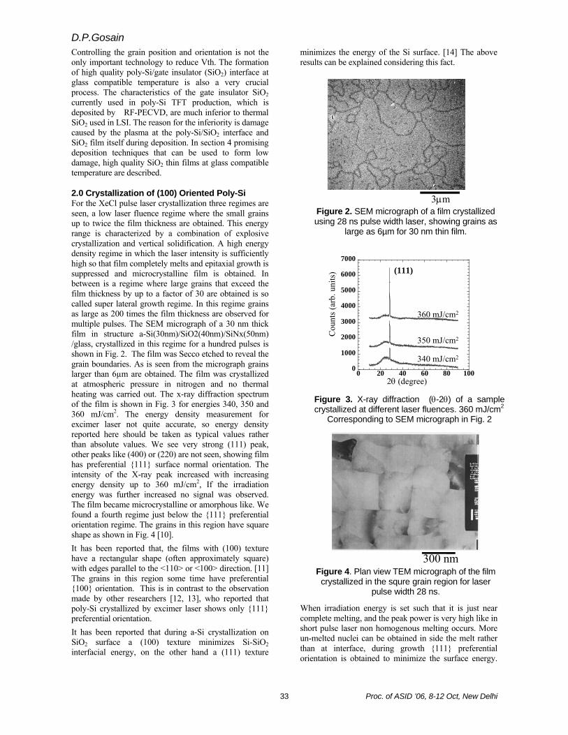
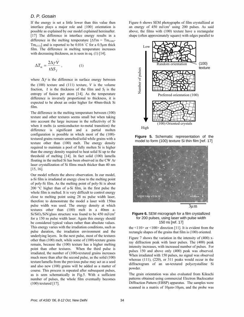
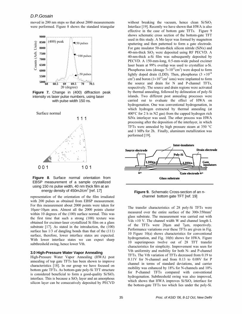
2.0 Crystallization of (100) Oriented Poly-Si For the XeCl pulse laser crystallization three regimes are seen, a low laser fluence regime where the small grains up to twice the film thickness are obtained. This energy range is characterized by a combination of explosive crystallization and vertical solidification. A high energy density regime in which the laser intensity is sufficiently high so that film completely melts and epitaxial growth is suppressed and microcrystalline film is obtained. In between is a regime where large grains that exceed the film thickness by up to a factor of 30 are obtained is so called super lateral growth regime. In this regime grains as large as 200 times the film thickness are observed for multiple pulses. The SEM micrograph of a 30 nm thick film in structure a-Si(30nm)/SiO2(40nm)/SiNx(50nm) /glass, crystallized in this regime for a hundred pulses is shown in Fig. 2. The film was Secco etched to reveal the grain boundaries. As is seen from the micrograph grains larger than 6µm are obtained. The film was crystallized at atmospheric pressure in nitrogen and no thermal heating was carried out. The x-ray diffraction spectrum of the film is shown in Fig. 3 for energies 340, 350 and 360 mJ/cm2. The energy density measurement for excimer laser not quite accurate, so energy density reported here should be taken as typical values rather than absolute values. We see very strong (111) peak, other peaks like (400) or (220) are not seen, showing film has preferential {111} surface normal orientation. The intensity of the X-ray peak increased with increasing energy density up to 360 mJ/cm2, If the irradiation energy was further increased no signal was observed. The film became microcrystalline or amorphous like. We found a fourth regime just below the {111} preferential orientation regime. The grains in this region have square shape as shown in Fig. 4 [10]. It has been reported that, the films with (100) texture have a rectangular shape (often approximately square) with edges parallel to the <110> or <100> direction. [11] The grains in this region some time have preferential {100} orientation. This is in contrast to the observation made by other researchers [12, 13], who reported that poly-Si crystallized by excimer laser shows only {111} preferential orientation. It has been reported that during a-Si crystallization on SiO2 surface a (100) texture minimizes Si-SiO2 interfacial energy, on the other hand a (111) texture
minimizes the energy of the Si surface. [14] The above results can be explained considering this fact.
When irradiation energy is set such that it is just near complete melting, and the peak power is very high like in short pulse laser non homogenous melting occurs. More un-melted nuclei can be obtained in side the melt rather than at interface, during growth {111} preferential orientation is obtained to minimize the surface energy.
Figure 2. SEM micrograph of a film crystallized using 28 ns pulse width laser, showing grains as
large as 6µm for 30 nm thin film.
3μm
Figure 3. X-ray diffraction (θ-2θ) of a sample crystallized at different laser fluences. 360 mJ/cm2
Corresponding to SEM micrograph in Fig. 2
0
1000
2000
3000
4000
5000
6000
7000
0 20 40 60 80 1002θ (degree)
(111)
340 mJ/cm2
350 mJ/cm2
360 mJ/cm2
Cou
nts (
arb.
uni
ts)
Figure 4. Plan view TEM micrograph of the film crystallized in the squre grain region for laser
pulse width 28 ns.
300 nm
D. P. Gosain
Proc. of ASID ’06, 8-12 Oct, New Delhi
34
If the energy is set a little lower than this value then interface plays a major role and {100} orientation is possible as explained by our model explained hereinafter. [17] The difference in interface energy results in a difference in the melting temperature [ΔTm = Tm(100)-Tm(111)] and is reported to be 0.016 °C for a 0.5μm thick film. The difference in melting temperature increases with decreasing thickness, as is seen in eq. (1) [14].
f
m StVT
ΔΔ
=Δ
−
γ2 , (1)
where γΔ is the difference in surface energy between the (100) texture and (111) texture, V is the volume fraction, t is the thickness of the film and Sf is the entropy of fusion per atom [14]. As the temperature difference is inversely proportional to thickness, it is expected to be about an order higher for 40nm-thick Si film. The difference in the melting temperature between (100) texture and other textures seems small but when taking into account the large increase in the reflectivity of Si when it melts (a semiconductor–to-metal transition) the difference is significant and a partial molten configuration is possible in which most of the (100)-textured grains remain unmelted/solid while grains with a texture other than (100) melt. The energy density required to maintain a pool of fully molten Si is higher than the energy density required to heat solid Si up to the threshold of melting [14]. In fact solid (100) lamella floating in the melted Si has been observed in the CW Ar laser crystallization of Si films much thicker than 40 nm [15, 16]. Our model reflects the above observation. In our model, a-Si film is irradiated at energy close to the melting point of poly-Si film. As the melting point of poly-Si is about 200 °C higher than of a-Si film, in the first pulse the whole film is melted. It is very difficult to control energy close to melting point using 28 ns pulse width laser, therefore to demonstrate the model a laser with 150ns pulse width was used. The energy density at which textures other than (100) melt in a 40nm a-Si/SiO2/SiN/glass structure was found to be 450 mJ/cm2 for a 150 ns pulse width laser. Again this energy should be considered typical values rather than absolute values. This energy varies with the irradiation conditions, such as pulse duration, the irradiation environment and the underlying layers. In the next pulse, most of the textures other than (100) melt, while some of (100)-texture grains remain, because the (100) texture has a higher melting point than other textures. When the third pulse is irradiated, the number of (100)-textured grains increases much more than after the second pulse, as the solid (100) texture/lamella from the previous pulse may act as a seed and also new (100) grains will be added as a matter of course. This process is repeated after subsequent pulses, as is seen schematically in Fig.5. With a sufficient number of pulses, the whole film eventually becomes (100) textured [17].
Figure 6 shows SEM photographs of film crystallized at an energy of 450 mJ/cm2 using 200 pulses. As said above, the films with (100) texture have a rectangular shape (often approximately square) with edges parallel to
the <110> or <100> direction [11]. It is evident from the rectangle shapes of the grains that film is (100) oriented. Figure 7 shows the variation in the intensity of (400) x-ray diffraction peak with laser pulses. The (400) peak intensity increases, with increased number of pulses. For pulses 150 and above only (400) peak was observed. When irradiated with 150 pulses, no signal was observed whereas (111), (220), or 311 peaks would occur in the diffractogram of an un-textured polycrystalline Si powder. The grain orientation was also evaluated from Kikuchi patterns obtained using commercial Electron Backscatter Diffraction Pattern (EBSP) apparatus. The samples were scanned in a matrix of 10μm×10μm, and the probe was
3μmFigure 6. SEM micrograph for a film crystallized
for 200 pulses, using laser with pulse width 150 ns [ref. 17]
Random orientation
Num
ber o
f pul
ses
Low
High
Preferred orientation (100)
(100) Oriented crystals
Figure 5. Schematic representation of the model to form (100) texture Si thin film [ref. 17]
(100) texture
D.P.Gosain
Proc. of ASID ’06, 8-12 Oct, New Delhi
35
moved in 200 nm steps so that about 2000 measurements were performed. Figure 8 shows the standard triangular
representation of the orientation of the film irradiated with 200 pulses as obtained from EBSP measurement. For this measurement about 2000 points were taken for 10μm×10μm area. Almost all the 2000 points cluster within 10 degrees of the (100) surface normal. This was the first time that such a strong (100) texture was obtained for excimer-laser crystallized Si film on a glass substrate [17]. As stated in the introduction, the (100) surface has 1/3 of dangling bonds than that of the (111) surface, therefore, lower interface states are expected. With lower interface states we can expect sharp subthreshold swing, hence lower Vth.
3.0 High-Pressure Water Vapor Annealing High-Pressure Water Vapor Annealing (HWA) post annealing of top gate TFTs has been shown to improve characteristics [18]. In our group we have focused on bottom gate TFTs. As bottom-gate poly-Si TFT structure is considered beneficial to form a good-quality Si/SiO2 interface. This is because a SiO2 layer and an amorphous silicon layer can be consecutively deposited by PECVD
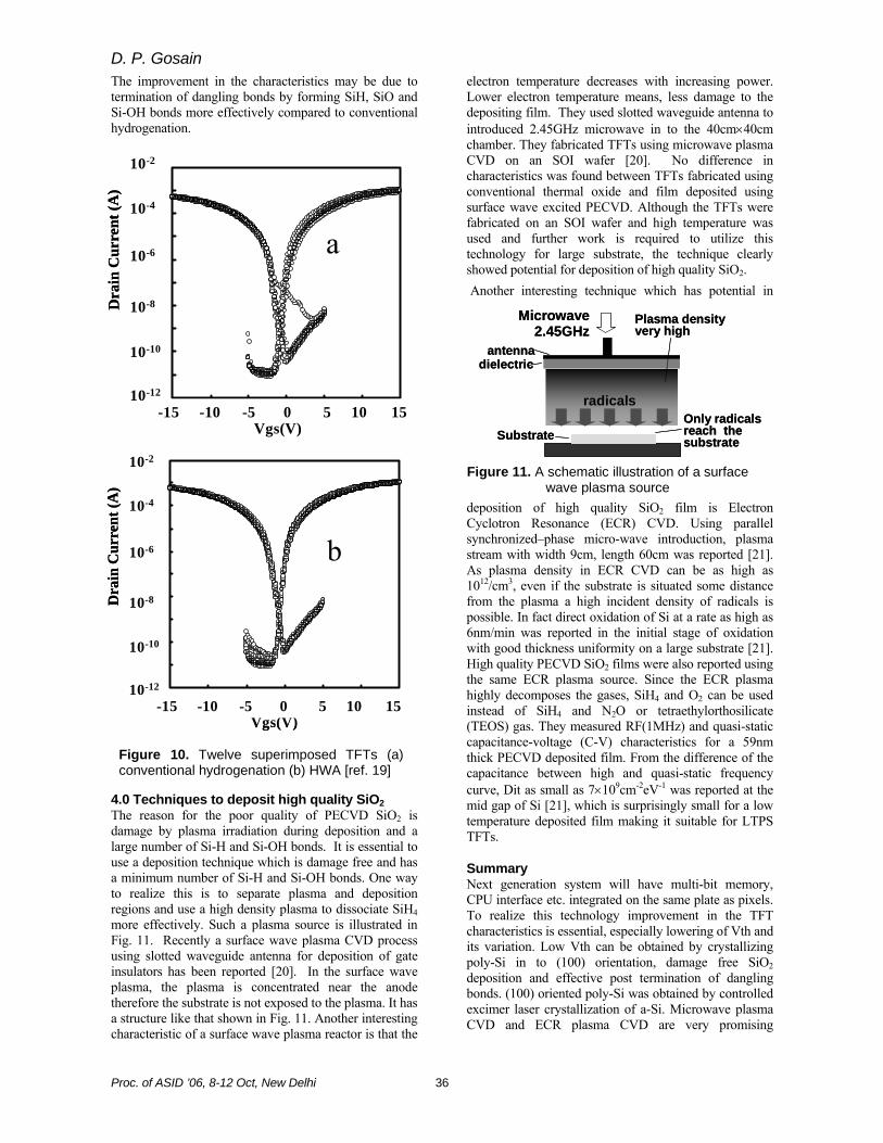
without breaking the vacuum, hence clean Si/SiO2 Interface [19]. Recently we have shown that HWA is also effective in the case of bottom gate TFTs. Figure 9 shows schematic cross section of the bottom-gate TFT used in this study. A Mo layer was formed by magnetron sputtering and then patterned to form a gate electrode. For gate insulator 50-nm-thick silicon nitride (SiNx) and 40-nm-thick SiO2 were deposited using RF PECVD. A 40-nm-thick a-Si film was subsequently deposited by PECVD. A 150-mm-long, 0.5-mm-wide pulsed excimer laser beam at 99% overlap was used to crystallize a-Si. Phosphorus ions (dosage 7×1012cm2) were doped to form lightly doped drain (LDD). Then, phosphorus (3 ×1014 cm2) and boron (1×1015cm2 ions) were implanted to form the source and drain for N and P-channel TFTs, respectively. The source and drain regions were activated by thermal annealing, followed by delineation of poly-Si islands. Two different post annealing processes were carried out to evaluate the effect of HWA on hydrogenation. One was conventional hydrogenation, in which hydrogen extracted by thermal annealing (at 400°C for 2 h in N2 gas) from the capped hydrogen rich SiNx interlayer was used. The other process was HWA processing after the deposition of the interlayer, in which TFTs were annealed by high pressure steam at 350 °C and 1 MPa for 2h. Finally, aluminum metallization was performed [19].
The transfer characteristics of 28 poly-Si TFTs were measured over the entire surface of the 300×350mm2 glass substrate. The measurement was carried out with Vds ±10 V. The channel width W and channel length L of the TFTs were 20µm and 7µm, respectively. Performance variations over these TFTs are given in Fig. 10 Figure 10(a) shows characteristics for conventional hydrogenation, and Fig. 10(b) shows for HWA. Figure 10 superimposes twelve out of 28 TFT transfer characteristics for simplicity. Improvement was seen for Vth uniformity and mobility for both N- and P-channel TFTs. The Vth variation of TFTs decreased from 0.19 to 0.11V for N-channel and from 0.13 to 0.08V for P channel in terms of standard deviations, and carrier mobility was enhanced by 18% for N-channels and 10% for P-channel TFTs compared with conventional hydrogenation. Subthreshold swing was also improved, which shows that HWA improves Si/SiO2 interface for the bottom-gate TFTs too which lies under the poly-Si.
Figure 7. Change in (400) diffraction peak intensity vs laser pulse numbers, using laser
with pulse width 150 ns.
Cou
nts
(Arb
. Uni
ts)
5000
5500
6000
6500
7000
7500
8000
8500
9000
68 68.5 69 69.5 70 70.52θ (degree)
(400) peak 150 pulses
100 pulses
50 pulses
Figure 8. Surface normal orientation from EBSP measurement of a sample crystallized using 150 ns pulse width, 40 nm thick film at an
energy density of 450mJ/cm2 [ref. 17]
Surface normal
Glass substrateGate electrode
Inter-insulators
Source electrode Drain electrode
Gateinsulators
Poly-Si
LDD(n-) LDD(n-)
n+ n+
Glass substrateGate electrode
Inter-insulators
Source electrode Drain electrode
Gateinsulators
Poly-Si
LDD(n-) LDD(n-)
n+ n+
Figure 9. Schematic Cross-section of an n-channel bottom gate TFT [ref. 19]
D. P. Gosain
Proc. of ASID ’06, 8-12 Oct, New Delhi
36
The improvement in the characteristics may be due to termination of dangling bonds by forming SiH, SiO and Si-OH bonds more effectively compared to conventional hydrogenation.
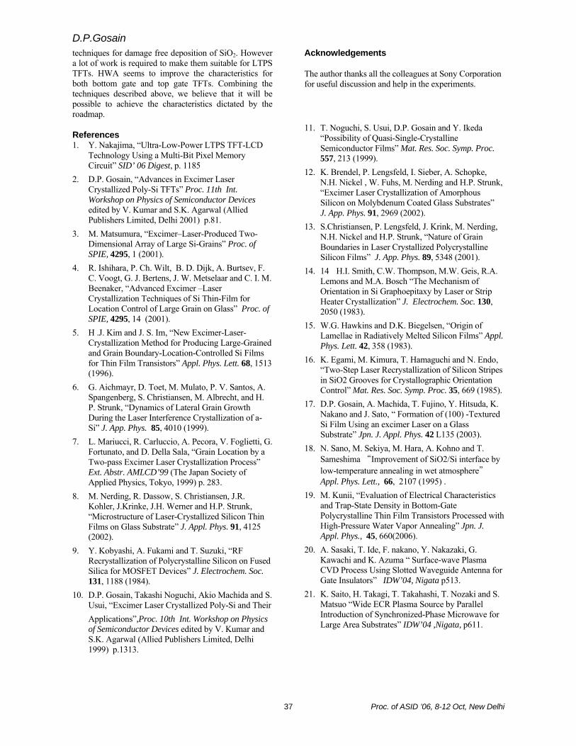
4.0 Techniques to deposit high quality SiO2 The reason for the poor quality of PECVD SiO2 is damage by plasma irradiation during deposition and a large number of Si-H and Si-OH bonds. It is essential to use a deposition technique which is damage free and has a minimum number of Si-H and Si-OH bonds. One way to realize this is to separate plasma and deposition regions and use a high density plasma to dissociate SiH4 more effectively. Such a plasma source is illustrated in Fig. 11. Recently a surface wave plasma CVD process using slotted waveguide antenna for deposition of gate insulators has been reported [20]. In the surface wave plasma, the plasma is concentrated near the anode therefore the substrate is not exposed to the plasma. It has a structure like that shown in Fig. 11. Another interesting characteristic of a surface wave plasma reactor is that the
electron temperature decreases with increasing power. Lower electron temperature means, less damage to the depositing film. They used slotted waveguide antenna to introduced 2.45GHz microwave in to the 40cm×40cm chamber. They fabricated TFTs using microwave plasma CVD on an SOI wafer [20]. No difference in characteristics was found between TFTs fabricated using conventional thermal oxide and film deposited using surface wave excited PECVD. Although the TFTs were fabricated on an SOI wafer and high temperature was used and further work is required to utilize this technology for large substrate, the technique clearly showed potential for deposition of high quality SiO2. Another interesting technique which has potential in
deposition of high quality SiO2 film is Electron Cyclotron Resonance (ECR) CVD. Using parallel synchronized–phase micro-wave introduction, plasma stream with width 9cm, length 60cm was reported [21]. As plasma density in ECR CVD can be as high as 1012/cm3, even if the substrate is situated some distance from the plasma a high incident density of radicals is possible. In fact direct oxidation of Si at a rate as high as 6nm/min was reported in the initial stage of oxidation with good thickness uniformity on a large substrate [21]. High quality PECVD SiO2 films were also reported using the same ECR plasma source. Since the ECR plasma highly decomposes the gases, SiH4 and O2 can be used instead of SiH4 and N2O or tetraethylorthosilicate (TEOS) gas. They measured RF(1MHz) and quasi-static capacitance-voltage (C-V) characteristics for a 59nm thick PECVD deposited film. From the difference of the capacitance between high and quasi-static frequency curve, Dit as small as 7×109cm-2eV-1 was reported at the mid gap of Si [21], which is surprisingly small for a low temperature deposited film making it suitable for LTPS TFTs.
Summary Next generation system will have multi-bit memory, CPU interface etc. integrated on the same plate as pixels. To realize this technology improvement in the TFT characteristics is essential, especially lowering of Vth and its variation. Low Vth can be obtained by crystallizing poly-Si in to (100) orientation, damage free SiO2 deposition and effective post termination of dangling bonds. (100) oriented poly-Si was obtained by controlled excimer laser crystallization of a-Si. Microwave plasma CVD and ECR plasma CVD are very promising
1.E-12
1.E-11
1.E-10
1.E-09
1.E-08
1.E-07
1.E-06
1.E-05
1.E-04
1.E-03
1.E-02
-15 -10 -5 0 5 10 15
Vgs(V)
Ids(A)
-15 -10 -5 0 5 10 15Vgs(V)
Dra
in C
urre
nt (A
)
10-2
10-4
10-6
10-8
10-10
10-12
a
1.E-12
1.E-11
1.E-10
1.E-09
1.E-08
1.E-07
1.E-06
1.E-05
1.E-04
1.E-03
1.E-02
-15 -10 -5 0 5 10 15
Vgs(V)
Ids(A)
-15 -10 -5 0 5 10 15Vgs(V)
Dra
in C
urre
nt (A
)
10-2
10-4
10-6
10-8
10-10
10-12
a
1.E -12
1.E -11
1.E -10
1.E -09
1.E -08
1.E -07
1.E -06
1.E -05
1.E -04
1.E -03
1.E -02
-15 -10 -5 0 5 10 15
Vgs(A)
Ids(A)
Vgs(V)
Dra
in C
urre
nt (A
)
10-2
10-4
10-6
10-8
10-10
10-12
-15 -10 -5 0 5 10 15
b
1.E -12
1.E -11
1.E -10
1.E -09
1.E -08
1.E -07
1.E -06
1.E -05
1.E -04
1.E -03
1.E -02
-15 -10 -5 0 5 10 15
Vgs(A)
Ids(A)
Vgs(V)
Dra
in C
urre
nt (A
)
10-2
10-4
10-6
10-8
10-10
10-12
-15 -10 -5 0 5 10 15
b
Figure 10. Twelve superimposed TFTs (a) conventional hydrogenation (b) HWA [ref. 19]
Figure 11. A schematic illustration of a surface wave plasma source
Microwave 2.45GHz
dielectric
radicals
Substrate
antenna
Plasma densityvery high
Only radicals reach the substrate
Microwave 2.45GHz
dielectric
radicals
Substrate
antenna
Plasma densityvery high
Only radicals reach the substrate
D.P.Gosain
Proc. of ASID ’06, 8-12 Oct, New Delhi
37
techniques for damage free deposition of SiO2. However a lot of work is required to make them suitable for LTPS TFTs. HWA seems to improve the characteristics for both bottom gate and top gate TFTs. Combining the techniques described above, we believe that it will be possible to achieve the characteristics dictated by the roadmap.
Acknowledgements
The author thanks all the colleagues at Sony Corporation for useful discussion and help in the experiments.
References 1. Y. Nakajima, “Ultra-Low-Power LTPS TFT-LCD
Technology Using a Multi-Bit Pixel Memory Circuit” SID’ 06 Digest, p. 1185
2. D.P. Gosain, “Advances in Excimer Laser Crystallized Poly-Si TFTs” Proc. 11th Int. Workshop on Physics of Semiconductor Devices edited by V. Kumar and S.K. Agarwal (Allied Publishers Limited, Delhi 2001) p.81.
3. M. Matsumura, “Excimer–Laser-Produced Two-Dimensional Array of Large Si-Grains” Proc. of SPIE, 4295, 1 (2001).
4. R. Ishihara, P. Ch. Wilt, B. D. Dijk, A. Burtsev, F. C. Voogt, G. J. Bertens, J. W. Metselaar and C. I. M. Beenaker, “Advanced Excimer –Laser Crystallization Techniques of Si Thin-Film for Location Control of Large Grain on Glass” Proc. of SPIE, 4295, 14 (2001).
5. H .J. Kim and J. S. Im, “New Excimer-Laser-Crystallization Method for Producing Large-Grained and Grain Boundary-Location-Controlled Si Films for Thin Film Transistors” Appl. Phys. Lett. 68, 1513 (1996).
6. G. Aichmayr, D. Toet, M. Mulato, P. V. Santos, A. Spangenberg, S. Christiansen, M. Albrecht, and H. P. Strunk, “Dynamics of Lateral Grain Growth During the Laser Interference Crystallization of a-Si” J. App. Phys. 85, 4010 (1999).
7. L. Mariucci, R. Carluccio, A. Pecora, V. Foglietti, G. Fortunato, and D. Della Sala, “Grain Location by a Two-pass Excimer Laser Crystallization Process” Ext. Abstr. AMLCD’99 (The Japan Society of Applied Physics, Tokyo, 1999) p. 283.
8. M. Nerding, R. Dassow, S. Christiansen, J.R. Kohler, J.Krinke, J.H. Werner and H.P. Strunk, “Microstructure of Laser-Crystallized Silicon Thin Films on Glass Substrate” J. Appl. Phys. 91, 4125 (2002).
9. Y. Kobyashi, A. Fukami and T. Suzuki, “RF Recrystallization of Polycrystalline Silicon on Fused Silica for MOSFET Devices” J. Electrochem. Soc. 131, 1188 (1984).
10. D.P. Gosain, Takashi Noguchi, Akio Machida and S. Usui, “Excimer Laser Crystallized Poly-Si and Their Applications”,Proc. 10th Int. Workshop on Physics of Semiconductor Devices edited by V. Kumar and S.K. Agarwal (Allied Publishers Limited, Delhi 1999) p.1313.
11. T. Noguchi, S. Usui, D.P. Gosain and Y. Ikeda “Possibility of Quasi-Single-Crystalline Semiconductor Films” Mat. Res. Soc. Symp. Proc. 557, 213 (1999).
12. K. Brendel, P. Lengsfeld, I. Sieber, A. Schopke, N.H. Nickel , W. Fuhs, M. Nerding and H.P. Strunk, “Excimer Laser Crystallization of Amorphous Silicon on Molybdenum Coated Glass Substrates” J. App. Phys. 91, 2969 (2002).
13. S.Christiansen, P. Lengsfeld, J. Krink, M. Nerding, N.H. Nickel and H.P. Strunk, “Nature of Grain Boundaries in Laser Crystallized Polycrystalline Silicon Films” J. App. Phys. 89, 5348 (2001).
14. 14 H.I. Smith, C.W. Thompson, M.W. Geis, R.A. Lemons and M.A. Bosch “The Mechanism of Orientation in Si Graphoepitaxy by Laser or Strip Heater Crystallization” J. Electrochem. Soc. 130, 2050 (1983).
15. W.G. Hawkins and D.K. Biegelsen, “Origin of Lamellae in Radiatively Melted Silicon Films” Appl. Phys. Lett. 42, 358 (1983).
16. K. Egami, M. Kimura, T. Hamaguchi and N. Endo, “Two-Step Laser Recrystallization of Silicon Stripes in SiO2 Grooves for Crystallographic Orientation Control” Mat. Res. Soc. Symp. Proc. 35, 669 (1985).
17. D.P. Gosain, A. Machida, T. Fujino, Y. Hitsuda, K. Nakano and J. Sato, “ Formation of (100) -Textured Si Film Using an excimer Laser on a Glass Substrate” Jpn. J. Appl. Phys. 42 L135 (2003).
18. N. Sano, M. Sekiya, M. Hara, A. Kohno and T. Sameshima “Improvement of SiO2/Si interface by low-temperature annealing in wet atmosphere” Appl. Phys. Lett., 66, 2107 (1995) .
19. M. Kunii, “Evaluation of Electrical Characteristics and Trap-State Density in Bottom-Gate Polycrystalline Thin Film Transistors Processed with High-Pressure Water Vapor Annealing” Jpn. J. Appl. Phys., 45, 660(2006).
20. A. Sasaki, T. Ide, F. nakano, Y. Nakazaki, G. Kawachi and K. Azuma “ Surface-wave Plasma CVD Process Using Slotted Waveguide Antenna for Gate Insulators” IDW’04, Nigata p513.
21. K. Saito, H. Takagi, T. Takahashi, T. Nozaki and S. Matsuo “Wide ECR Plasma Source by Parallel Introduction of Synchronized-Phase Microwave for Large Area Substrates” IDW’04 ,Nigata, p611.


![Thickness map [nm] of the poly-Si layer of a poly-Si/SiO 2 /Si multi-layer structure](https://static.fdocuments.in/doc/165x107/568137b4550346895d9f5613/thickness-map-nm-of-the-poly-si-layer-of-a-poly-sisio-2-si-multi-layer.jpg)
