Low-Power, 16-Bit, 1-MHz, Single/Dual Unipolar Input, …€¢Multi-Chip Daisy Chain Mode Single...
50
1FEATURES APPLICATIONS DESCRIPTION REF- +IN REF+ SDI SCLK SDO CDAC SAR COMPARATOR OUTPUT LATCH and 3-STATE DRIVER CONVERSION and CONTROL LOGIC -IN +IN1 +IN0 COM NC OSC _ + ADS8330 ADS8329 FS/CS CONVST EOC/INT /CDI ADS8329 ADS8330 www.ti.com ................................................................................................................................................... SLAS516C–DECEMBER 2006–REVISED JULY 2009 LOW-POWER, 16-BIT, 1-MHz, SINGLE/DUAL UNIPOLAR INPUT, ANALOG-TO-DIGITAL CONVERTERS WITH SERIAL INTERFACE • Communications 2• 2.7-V to 5.5-V Analog Supply, Low Power: • Transducer Interface – 15.5 mW (1 MHz, +VA = 3 V, +VBD = 1.8 V) • Medical Instruments • 1-MHz Sampling Rate 3 V ≤ +VA ≤ 5.5 V, • Magnetometers 900-kHz Sampling Rate 2.7 V ≤ +VA ≤ 3V • Industrial Process Control • Excellent DC Performance: • Data Acquisition Systems ±1.0 LSB Typ, ±1.75 LSB Max INL ±0.5 LSB Typ, ±1 LSB Max DNL • Automatic Test Equipment 16-Bit NMC Over Temperature ±0.5 mV Max Offset Error at 3 V ±1 mV Max Offset Error at 5 V The ADS8329 is a low-power, 16-bit, 1-MSPS • Excellent AC Performance at f I = 10 kHz with analog-to-digital converter (ADC) with a unipolar 93 dB SNR, 105 dB SFDR, –102 dB THD input. The device includes a 16-bit capacitor-based SAR ADC with inherent sample-and-hold. • Built-In Conversion Clock (CCLK) • 1.65 V to 5.5 V I/O Supply: The ADS8330 is based on the same core and includes a 2-to-1 input MUX with programmable SPI/DSP Compatible Serial option of TAG bit output. Both the ADS8329 and SCLK up to 50 MHz ADS8330 offer a high-speed, wide voltage serial • Comprehensive Power-Down Modes: interface and are capable of chain mode operation Deep Power-Down when multiple converters are used. Nap Power-Down These converters are available in 4 × 4 QFN and Auto Nap Power-Down 16-pin TSSOP packages, and are fully specified for • Unipolar Input Range: 0 V to V REF operation over the industrial –40°C to +85°C • Software Reset temperature range. • Global CONVST (Independent of CS) Low Power, High-Speed SAR Converter Family • Programmable Status/Polarity EOC/INT Type/Speed 500 kSPS 1 MSPS • 16-Pin 4 × 4 QFN and 16-Pin TSSOP Packages Single ADS8327 ADS8329 • Multi-Chip Daisy Chain Mode 16-bit single-ended Dual ADS8328 ADS8330 • Programmable TAG Bit Output Single — ADS7279 14-bit single-ended • Auto/Manual Channel Select Mode (ADS8330) Dual — ADS7280 Single — ADS7229 12-bit single ended Dual — ADS7230 1 Please be aware that an important notice concerning availability, standard warranty, and use in critical applications of Texas Instruments semiconductor products and disclaimers thereto appears at the end of this data sheet. 2All trademarks are the property of their respective owners. PRODUCTION DATA information is current as of publication date. Copyright © 2006–2009, Texas Instruments Incorporated Products conform to specifications per the terms of the Texas Instruments standard warranty. Production processing does not necessarily include testing of all parameters.
-
Upload
trinhnguyet -
Category
Documents
-
view
217 -
download
1
Transcript of Low-Power, 16-Bit, 1-MHz, Single/Dual Unipolar Input, …€¢Multi-Chip Daisy Chain Mode Single...

1FEATURES APPLICATIONS
DESCRIPTION
REF−
+IN
REF+SDISCLK
SDO
CDAC
SAR
COMPARATOR
OUTPUTLATCH
and3−STATEDRIVER
CONVERSIONand
CONTROLLOGIC
−IN
+IN1
+IN0
COM
NC
OSC
_+
ADS8330 ADS8329
FS/CS
CONVSTEOC/INT/CDI
ADS8329ADS8330
www.ti.com ................................................................................................................................................... SLAS516C–DECEMBER 2006–REVISED JULY 2009
LOW-POWER, 16-BIT, 1-MHz, SINGLE/DUAL UNIPOLAR INPUT,ANALOG-TO-DIGITAL CONVERTERS WITH SERIAL INTERFACE
• Communications2• 2.7-V to 5.5-V Analog Supply, Low Power:• Transducer Interface– 15.5 mW (1 MHz, +VA = 3 V, +VBD = 1.8 V)• Medical Instruments• 1-MHz Sampling Rate 3 V ≤ +VA ≤ 5.5 V,• Magnetometers900-kHz Sampling Rate 2.7 V ≤ +VA ≤ 3 V• Industrial Process Control• Excellent DC Performance:• Data Acquisition Systems±1.0 LSB Typ, ±1.75 LSB Max INL
±0.5 LSB Typ, ±1 LSB Max DNL • Automatic Test Equipment16-Bit NMC Over Temperature±0.5 mV Max Offset Error at 3 V±1 mV Max Offset Error at 5 V The ADS8329 is a low-power, 16-bit, 1-MSPS
• Excellent AC Performance at fI = 10 kHz with analog-to-digital converter (ADC) with a unipolar93 dB SNR, 105 dB SFDR, –102 dB THD input. The device includes a 16-bit capacitor-based
SAR ADC with inherent sample-and-hold.• Built-In Conversion Clock (CCLK)• 1.65 V to 5.5 V I/O Supply: The ADS8330 is based on the same core and
includes a 2-to-1 input MUX with programmableSPI/DSP Compatible Serialoption of TAG bit output. Both the ADS8329 andSCLK up to 50 MHzADS8330 offer a high-speed, wide voltage serial• Comprehensive Power-Down Modes: interface and are capable of chain mode operationDeep Power-Down when multiple converters are used.
Nap Power-DownThese converters are available in 4 × 4 QFN andAuto Nap Power-Down16-pin TSSOP packages, and are fully specified for• Unipolar Input Range: 0 V to VREF operation over the industrial –40°C to +85°C
• Software Reset temperature range.• Global CONVST (Independent of CS)
Low Power, High-Speed SAR Converter Family• Programmable Status/Polarity EOC/INTType/Speed 500 kSPS 1 MSPS• 16-Pin 4 × 4 QFN and 16-Pin TSSOP Packages
Single ADS8327 ADS8329• Multi-Chip Daisy Chain Mode 16-bit single-endedDual ADS8328 ADS8330• Programmable TAG Bit OutputSingle — ADS7279
14-bit single-ended• Auto/Manual Channel Select Mode (ADS8330)Dual — ADS7280Single — ADS7229
12-bit single endedDual — ADS7230
1
Please be aware that an important notice concerning availability, standard warranty, and use in critical applications of TexasInstruments semiconductor products and disclaimers thereto appears at the end of this data sheet.
2All trademarks are the property of their respective owners.
PRODUCTION DATA information is current as of publication date. Copyright © 2006–2009, Texas Instruments IncorporatedProducts conform to specifications per the terms of the TexasInstruments standard warranty. Production processing does notnecessarily include testing of all parameters.

ABSOLUTE MAXIMUM RATINGS
ADS8329ADS8330
SLAS516C–DECEMBER 2006–REVISED JULY 2009 ................................................................................................................................................... www.ti.com
These devices have limited built-in ESD protection. The leads should be shorted together or the device placed in conductive foamduring storage or handling to prevent electrostatic damage to the MOS gates.
ORDERING INFORMATION (1)
MAXIMUM MAXIMUM MAXIMUMINTEGRAL DIFFERENTIAL OFFSET TRANSPORTLINEARITY LINEARITY ERROR PACKAGE PACKAGE TEMPERATURE ORDERING MEDIA,
MODEL (LSB) (LSB) (mV) TYPE DESIGNATOR RANGE INFORMATION QUANTITY
ADS8329IRSAT Small tape and reel, 2504 × 4 QFN-16 RSA
ADS8329IRSAR Tape and reel, 3000ADS8329I ±2.5 –1/+2 ±0.8 –40°C to +85°C
ADS8329IPW Tube, 90TSSOP-16 PW
ADS8329IPWR Tape and reel, 2000
ADS8329IBRSAT Small tape and reel, 2504 × 4 QFN-16 RSA
ADS8329IBRSAR Tape and reel, 3000ADS8329IB ±1.75 ±1 ±0.5 –40°C to +85°C
ADS8329IBPW Tube, 90TSSOP-16 PW
ADS8329IBPWR Tape and reel, 2000
ADS8330IRSAT Small tape and reel, 2504 × 4 QFN-16 RSA
ADS8330IRSAR Tape and reel, 3000ADS8330I ±2.5 –1/+2 ±0.8 –40°C to +85°C
ADS8330IPW Tube, 90TSSOP-16 PW
ADS8330IPWR Tape and reel, 2000
ADS8330IBRSAT Small tape and reel, 2504 × 4 QFN-16 RSA
ADS8330IBRSAR Tape and reel, 3000ADS8330IB ±1.75 ±1 ±0.5 –40°C to +85°C
ADS8330IBPW Tube, 90TSSOP-16 PW
ADS8330IBPWR Tape and reel, 2000
(1) For the most current package and ordering information see the Package Option Addendum at the end of this document, or see the TIweb site at www.ti.com.
Over operating free-air temperature range, unless otherwise noted. (1)
UNIT+IN to AGND –0.3 V to +VA + 0.3 V
Voltage–IN to AGND –0.3 V to +VA + 0.3 V+VA to AGND –0.3 V to 7 V+REF to AGND –0.3 V to +VA + 0.3 V
Voltage range –REF to AGND –0.3 V to 0.3 V+VBD to BDGND –0.3 V to 7 VAGND to BDGND –0.3 V to 0.3 V
Digital input voltage to BDGND –0.3 V to +VBD + 0.3 VDigital output voltage to BDGND –0.3 V to +VBD + 0.3 V
TA Operating free-air temperature range –40°C to +85°CTstg Storage temperature range –65°C to +150°C
Junction temperature (TJ max) +150°CPower dissipation (TJMax – TA)/θJA4 × 4 QFN-16
package θJA thermal impedance +47°C/WPower dissipation (TJMax – TA)/θJATSSOP-16
package θJA thermal impedance +86°C/W
(1) Stresses beyond those listed under absolute maximum ratings may cause permanent damage to the device. These are stress ratingsonly, and functional operation of the device at these or any other conditions beyond those indicated under recommended operatingconditions is not implied. Exposure to absolute-maximum-rated conditions for extended periods may affect device reliability.
2 Submit Documentation Feedback Copyright © 2006–2009, Texas Instruments Incorporated
Product Folder Link(s): ADS8329 ADS8330
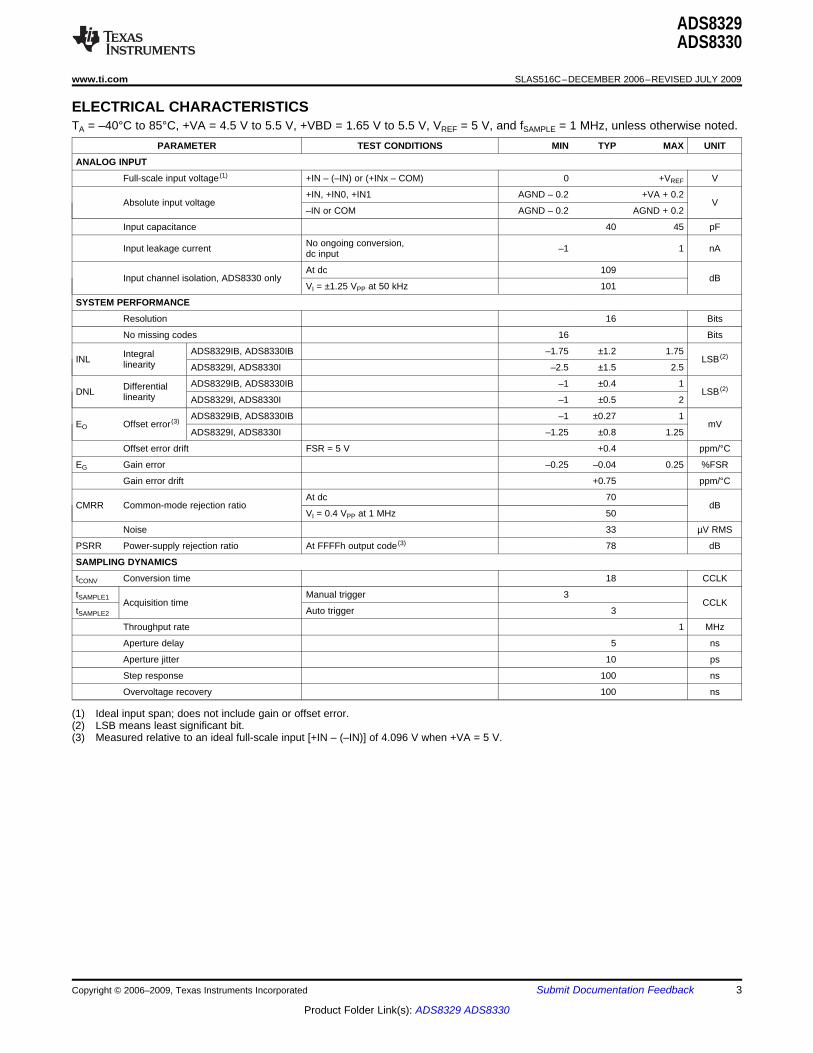
ELECTRICAL CHARACTERISTICS
ADS8329ADS8330
www.ti.com ................................................................................................................................................... SLAS516C–DECEMBER 2006–REVISED JULY 2009
TA = –40°C to 85°C, +VA = 4.5 V to 5.5 V, +VBD = 1.65 V to 5.5 V, VREF = 5 V, and fSAMPLE = 1 MHz, unless otherwise noted.PARAMETER TEST CONDITIONS MIN TYP MAX UNIT
ANALOG INPUT
Full-scale input voltage (1) +IN – (–IN) or (+INx – COM) 0 +VREF V
+IN, +IN0, +IN1 AGND – 0.2 +VA + 0.2Absolute input voltage V
–IN or COM AGND – 0.2 AGND + 0.2
Input capacitance 40 45 pF
No ongoing conversion,Input leakage current –1 1 nAdc input
At dc 109Input channel isolation, ADS8330 only dB
VI = ±1.25 VPP at 50 kHz 101
SYSTEM PERFORMANCE
Resolution 16 Bits
No missing codes 16 Bits
ADS8329IB, ADS8330IB –1.75 ±1.2 1.75IntegralINL LSB (2)linearity ADS8329I, ADS8330I –2.5 ±1.5 2.5
ADS8329IB, ADS8330IB –1 ±0.4 1DifferentialDNL LSB (2)linearity ADS8329I, ADS8330I –1 ±0.5 2
ADS8329IB, ADS8330IB –1 ±0.27 1EO Offset error (3) mV
ADS8329I, ADS8330I –1.25 ±0.8 1.25
Offset error drift FSR = 5 V +0.4 ppm/°C
EG Gain error –0.25 –0.04 0.25 %FSR
Gain error drift +0.75 ppm/°C
At dc 70CMRR Common-mode rejection ratio dB
VI = 0.4 VPP at 1 MHz 50
Noise 33 µV RMS
PSRR Power-supply rejection ratio At FFFFh output code (3) 78 dB
SAMPLING DYNAMICS
tCONV Conversion time 18 CCLK
tSAMPLE1 Manual trigger 3Acquisition time CCLK
tSAMPLE2 Auto trigger 3
Throughput rate 1 MHz
Aperture delay 5 ns
Aperture jitter 10 ps
Step response 100 ns
Overvoltage recovery 100 ns
(1) Ideal input span; does not include gain or offset error.(2) LSB means least significant bit.(3) Measured relative to an ideal full-scale input [+IN – (–IN)] of 4.096 V when +VA = 5 V.
Copyright © 2006–2009, Texas Instruments Incorporated Submit Documentation Feedback 3
Product Folder Link(s): ADS8329 ADS8330

ADS8329ADS8330
SLAS516C–DECEMBER 2006–REVISED JULY 2009 ................................................................................................................................................... www.ti.com
ELECTRICAL CHARACTERISTICS (continued)TA = –40°C to 85°C, +VA = 4.5 V to 5.5 V, +VBD = 1.65 V to 5.5 V, VREF = 5 V, and fSAMPLE = 1 MHz, unless otherwise noted.
PARAMETER TEST CONDITIONS MIN TYP MAX UNIT
DYNAMIC CHARACTERISTICS
VIN = 5 VPP at 10 kHz –102THD Total harmonic distortion (4) dB
VIN = 5 VPP at 100 kHz –95
VIN = 5 VPP at 10 kHz 93
SNR Signal-to-noise ratio ADS8329/30IB 90 92 dBVIN = 5 VPP at 100 kHz
ADS8329/30I 90
VIN = 5 VPP at 10 kHz 92SINAD Signal-to-noise + distortion dB
VIN = 5 VPP at 100 kHz 90
VIN = 5 VPP at 10 kHz 105SFDR Spurious-free dynamic range dB
VIN = 5 VPP at 100 kHz 97
–3dB small-signal bandwidth 30 MHz
CLOCK
Internal conversion clock frequency 21 22.9 24.5 MHz
Used as I/O clock only 50SCLK external serial clock MHz
As I/O clock and conversion clock 1 42
EXTERNAL VOLTAGE REFERENCE INPUT
Input VREF[(REF+) – (REF–)] 5.5 V ≥ +VA ≥ 4.5 V 0.3 +VAVREF reference V
(REF–) – AGND –0.1 0.1range
Resistance (5) Reference input 40 kΩ
DIGITAL INPUT/OUTPUT
Logic family—CMOS
VIH High-level input voltage 5.5 V ≥ +VBD ≥ 4.5 V 0.65 × (+VBD) +VBD + 0.3 V
0.35 ×VIL Low-level input voltage 5.5 V ≥ +VBD ≥ 4.5 V –0.3 V(+VBD)
II Input current VI = +VBD or BDGND –50 50 nA
CI Input capacitance 5 pF
5.5 V ≥ +VBD ≥ 4.5 V,VOH High-level output voltage +VBD – 0.6 +VBD VIO = 100 µA
5.5 V ≥ +VBD ≥ 4.5 V,VOL Low-level output voltage 0 0.4 VIO = 100 µA
CO Output capacitance 5 pF
CL Load capacitance 30 pF
Data format—straight binary
POWER-SUPPLY REQUIREMENTS
+VBD 1.65 3.3 5.5 VPower-supplyvoltage +VA 4.5 5 5.5 V
1-MHz Sample rate 7.0 7.8mA
Supply current NAP/Auto-NAP mode 0.3 0.5
Deep power-down mode 4 50 nA
Buffer I/O supply current 1 MSPS 1.7 mA
+VA = 5 V, +VBD = 5 V 44 48Power dissipation mW
+VA = 5 V, +VBD = 1.8 V 35 39.5
TEMPERATURE RANGE
TA Operating free-air temperature –40 +85 °C
(4) Calculated on the first nine harmonics of the input frequency.(5) Can vary ±30%.
4 Submit Documentation Feedback Copyright © 2006–2009, Texas Instruments Incorporated
Product Folder Link(s): ADS8329 ADS8330

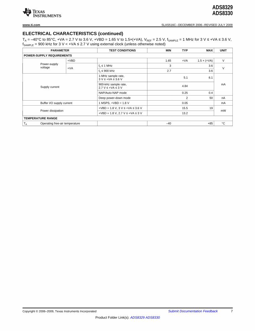
ELECTRICAL CHARACTERISTICS
ADS8329ADS8330
www.ti.com ................................................................................................................................................... SLAS516C–DECEMBER 2006–REVISED JULY 2009
TA = –40°C to 85°C, +VA = 2.7 V to 3.6 V, +VBD = 1.65 V to 1.5×(+VA), VREF = 2.5 V, fSAMPLE = 1 MHz for 3 V ≤ +VA ≤ 3.6 V,fSAMPLE = 900 kHz for 3 V < +VA ≤ 2.7 V using external clock (unless otherwise noted)
PARAMETER TEST CONDITIONS MIN TYP MAX UNIT
ANALOG INPUT
Full-scale input voltage (1) +IN – (–IN) or (+INx – COM) 0 +VREF V
+IN, +IN0, +IN1 AGND – 0.2 +VA + 0.2Absolute input voltage V
–IN or COM AGND – 0.2 AGND + 0.2
Input capacitance 40 45 pF
No ongoing conversion,Input leakage current –1 1 nADC Input
At dc 108Input channel isolation, ADS8330 only dB
VI = ±1.25 VPP at 50 kHz 101
SYSTEM PERFORMANCE
Resolution 16 Bits
No missing codes 16 Bits
ADS8329IB, –1.75 ±1 1.75ADS8330IBINL Integral linearity LSB (2)
ADS8329I, ADS8330I –2.5 ±1.5 2.5
ADS8329IB, –1 ±0.5 1Differential ADS8330IBDNL LSB (2)linearity
ADS8329I, ADS8330I –1 ±0.8 2
ADS8329IB, –0.5 ±0.05 0.5ADS8330IBEO Offset error (3) mVADS8329I, ADS8330I –0.8 ±0.2 0.8
Offset error drift FSR = 2.5 V +0.8 ppm/°C
EG Gain error –0.25 –0.04 0.25 %FSR
Gain error drift +0.5 ppm/°C
At dc 70CMRR Common-mode rejection ratio dB
VI = 0.4 VPP at 1 MHz 50
Noise 33 µV RMS
PSRR Power-supply rejection ratio At FFFFh output code (3) 78 dB
SAMPLING DYNAMICS
tCONV Conversion time 18 CCLK
tSAMPLE1 Manual trigger 3Acquisition time CCLK
tSAMPLE2 Auto trigger 3
Throughput rate 1 MHz
Aperture delay 5 ns
Aperture jitter 10 ps
Step response 100 ns
Overvoltage recovery 100 ns
(1) Ideal input span, does not include gain or offset error.(2) LSB means least significant bit.(3) Measured relative to an ideal full-scale input [+IN – (–IN)] of 2.5 V when +VA = 3 V.
Copyright © 2006–2009, Texas Instruments Incorporated Submit Documentation Feedback 5
Product Folder Link(s): ADS8329 ADS8330

ADS8329ADS8330
SLAS516C–DECEMBER 2006–REVISED JULY 2009 ................................................................................................................................................... www.ti.com
ELECTRICAL CHARACTERISTICS (continued)TA = –40°C to 85°C, +VA = 2.7 V to 3.6 V, +VBD = 1.65 V to 1.5×(+VA), VREF = 2.5 V, fSAMPLE = 1 MHz for 3 V ≤ +VA ≤ 3.6 V,fSAMPLE = 900 kHz for 3 V < +VA ≤ 2.7 V using external clock (unless otherwise noted)
PARAMETER TEST CONDITIONS MIN TYP MAX UNIT
DYNAMIC CHARACTERISTICS
VIN = 2.5 VPP at 10 kHz –102THD Total harmonic distortion (4) dB
VIN = 2.5 VPP at 100 kHz –93
VIN = 2.5 VPP at 10 kHz 89SNR Signal-to-noise ratio dB
VIN = 2.5 VPP at 100 kHz 88
VIN = 2.5 VPP at 10 kHz 88.5SINAD Signal-to-noise + distortion dB
VIN = 2.5 VPP at 100 kHz 88
VIN = 2.5 VPP at 10 kHz 104SFDR Spurious-free dynamic range dB
VIN = 2.5 VPP at 100 kHz 94.2
–3dB small-signal bandwidth 30 MHz
CLOCK
Internal conversion clock frequency 21 22.3 23.5 MHz
Used as I/O clock only 42SCLK external serial clock MHz
As I/O clock and conversion clock 1 42
EXTERNAL VOLTAGE REFERENCE INPUT
fSAMPLE ≤ 500kSPS, 0.3 2.5252.7 V ≤ +VA < 3V
fSAMPLE ≤ 500kSPS, 0.3 33 V ≤ +VA < 3.6VVREF[(REF+) –Input reference (REF–)]VREF fSAMPLE > 500kSPS, Vrange 2.475 2.5252.7 V ≤ +VA < 3V
fSAMPLE > 500kSPS, 2.475 33 V ≤ +VA ≤ 3.6V
(REF–) – AGND –0.1 0.1
Resistance (5) Reference input 40 kΩ
DIGITAL INPUT/OUTPUT
Logic family—CMOS
VIH High-level input voltage (+VA × 1.5) V ≥ +VBD ≥ 1.65 V 0.65 × (+VBD) +VBD + 0.3 V
VIL Low-level input voltage (+VA × 1.5) V ≥ +VBD ≥ 1.65 V –0.3 0.35 × (+VBD) V
II Input current VI = +VBD or BDGND –50 50 nA
CI Input capacitance 5 pF
(+VA × 1.5) V ≥ +VBD ≥ 1.65 V,VOH High-level output voltage +VBD – 0.6 +VBD VIO = 100 µA
(+VA × 1.5) V ≥ +VBD ≥ 1.65 V,VOL Low-level output voltage 0 0.4 VIO = 100 µA
CO Output capacitance 5 pF
CL Load capacitance 30 pF
Data format—straight binary
(4) Calculated on the first nine harmonics of the input frequency.(5) Can vary ±30%.
6 Submit Documentation Feedback Copyright © 2006–2009, Texas Instruments Incorporated
Product Folder Link(s): ADS8329 ADS8330
ADS8329ADS8330
www.ti.com ................................................................................................................................................... SLAS516C–DECEMBER 2006–REVISED JULY 2009
ELECTRICAL CHARACTERISTICS (continued)TA = –40°C to 85°C, +VA = 2.7 V to 3.6 V, +VBD = 1.65 V to 1.5×(+VA), VREF = 2.5 V, fSAMPLE = 1 MHz for 3 V ≤ +VA ≤ 3.6 V,fSAMPLE = 900 kHz for 3 V < +VA ≤ 2.7 V using external clock (unless otherwise noted)
PARAMETER TEST CONDITIONS MIN TYP MAX UNIT
POWER-SUPPLY REQUIREMENTS
+VBD 1.65 +VA 1.5 × (+VA) VPower-supply fs ≤ 1 MHz 3 3.6voltage +VA V
fs ≤ 900 kHz 2.7 3.6
1-MHz sample rate, 5.1 6.13 V ≤ +VA ≤ 3.6 V
900-kHz sample rate, mA4.84Supply current 2.7 V ≤ +VA ≤ 3 V
NAP/Auto-NAP mode 0.25 0.4
Deep power-down mode 2 50 nA
Buffer I/O supply current 1 MSPS, +VBD = 1.8 V 0.05 mA
+VBD = 1.8 V, 3 V ≤ +VA ≤ 3.6 V 15.5 19Power dissipation mW
+VBD = 1.8 V, 2.7 V ≤ +VA ≤ 3 V 13.2
TEMPERATURE RANGE
TA Operating free-air temperature –40 +85 °C
Copyright © 2006–2009, Texas Instruments Incorporated Submit Documentation Feedback 7
Product Folder Link(s): ADS8329 ADS8330

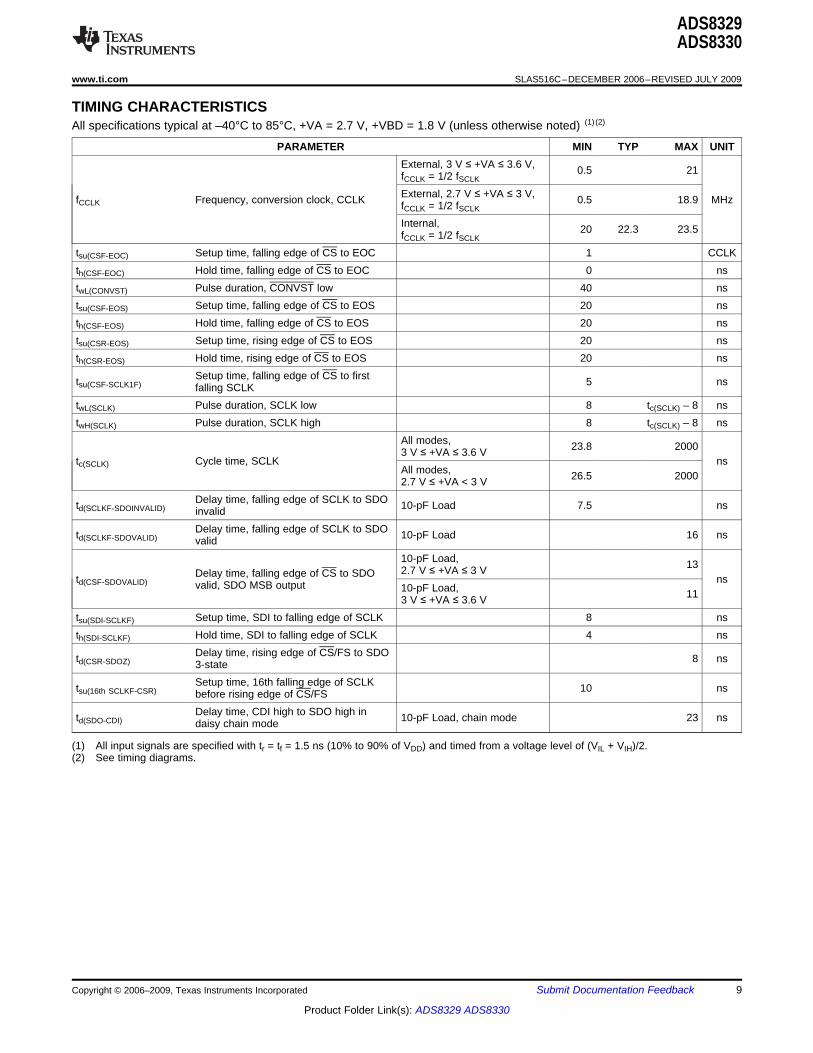
TIMING CHARACTERISTICS
ADS8329ADS8330
SLAS516C–DECEMBER 2006–REVISED JULY 2009 ................................................................................................................................................... www.ti.com
All specifications typical at –40°C to 85°C and +VA = +VBD = 5 V. (1) (2)
PARAMETER MIN TYP MAX UNITExternal, 0.5 21fCCLK = 1/2 fSCLKfCCLK Frequency, conversion clock, CCLK MHzInternal, 21 22.9 24.5fCCLK = 1/2 fSCLK
tsu(CSF-EOC) Setup time, falling edge of CS to EOC 1 CCLKth(CSF-EOC) Hold time, falling edge of CS to EOC 0 nstwL(CONVST) Pulse duration, CONVST low 40 nstsu(CSF-EOS) Setup time, falling edge of CS to EOS 20 nsth(CSF-EOS) Hold time, falling edge of CS to EOS 20 nstsu(CSR-EOS) Setup time, rising edge of CS to EOS 20 nsth(CSR-EOS) Hold time, rising edge of CS to EOS 20 ns
Setup time, falling edge of CS to first fallingtsu(CSF-SCLK1F) 5 nsSCLKtwL(SCLK) Pulse duration, SCLK low 8 tc(SCLK) – 8 nstwH(SCLK) Pulse duration, SCLK high 8 tc(SCLK) – 8 ns
I/O Clock only 20I/O and conversion clock 23.8 2000
tc(SCLK) Cycle time, SCLK nsI/O Clock, chain mode 20I/O and conversion clock, 23.8 2000chain mode
Delay time, falling edge of SCLK to SDOtd(SCLKF-SDOINVALID) 10-pF Load 2 nsinvalidDelay time, falling edge of SCLK to SDOtd(SCLKF-SDOVALID) 10-pF Load 10 nsvalidDelay time, falling edge of CS to SDOtd(CSF-SDOVALID) 10-pF Load 8.5 nsvalid, SDO MSB output
tsu(SDI-SCLKF) Setup time, SDI to falling edge of SCLK 8 nsth(SDI-SCLKF) Hold time, SDI to falling edge of SCLK 4 ns
Delay time, rising edge of CS/FS to SDOtd(CSR-SDOZ) 5 ns3-stateSetup time, 16th falling edge of SCLKtsu(16th SCLKF-CSR) 10 nsbefore rising edge of CS/FSDelay time, CDI high to SDO high in daisytd(SDO-CDI) 10-pF Load, chain mode 16 nschain mode
(1) All input signals are specified with tr = tf = 1.5 ns (10% to 90% of VDD) and timed from a voltage level of (VIL + VIH)/2.(2) See timing diagrams.
8 Submit Documentation Feedback Copyright © 2006–2009, Texas Instruments Incorporated
Product Folder Link(s): ADS8329 ADS8330
TIMING CHARACTERISTICS
ADS8329ADS8330
www.ti.com ................................................................................................................................................... SLAS516C–DECEMBER 2006–REVISED JULY 2009
All specifications typical at –40°C to 85°C, +VA = 2.7 V, +VBD = 1.8 V (unless otherwise noted) (1) (2)
PARAMETER MIN TYP MAX UNITExternal, 3 V ≤ +VA ≤ 3.6 V, 0.5 21fCCLK = 1/2 fSCLK
External, 2.7 V ≤ +VA ≤ 3 V,fCCLK Frequency, conversion clock, CCLK 0.5 18.9 MHzfCCLK = 1/2 fSCLK
Internal, 20 22.3 23.5fCCLK = 1/2 fSCLK
tsu(CSF-EOC) Setup time, falling edge of CS to EOC 1 CCLKth(CSF-EOC) Hold time, falling edge of CS to EOC 0 nstwL(CONVST) Pulse duration, CONVST low 40 nstsu(CSF-EOS) Setup time, falling edge of CS to EOS 20 nsth(CSF-EOS) Hold time, falling edge of CS to EOS 20 nstsu(CSR-EOS) Setup time, rising edge of CS to EOS 20 nsth(CSR-EOS) Hold time, rising edge of CS to EOS 20 ns
Setup time, falling edge of CS to firsttsu(CSF-SCLK1F) 5 nsfalling SCLKtwL(SCLK) Pulse duration, SCLK low 8 tc(SCLK) – 8 nstwH(SCLK) Pulse duration, SCLK high 8 tc(SCLK) – 8 ns
All modes, 23.8 20003 V ≤ +VA ≤ 3.6 Vtc(SCLK) Cycle time, SCLK ns
All modes, 26.5 20002.7 V ≤ +VA < 3 VDelay time, falling edge of SCLK to SDOtd(SCLKF-SDOINVALID) 10-pF Load 7.5 nsinvalidDelay time, falling edge of SCLK to SDOtd(SCLKF-SDOVALID) 10-pF Load 16 nsvalid
10-pF Load, 132.7 V ≤ +VA ≤ 3 VDelay time, falling edge of CS to SDOtd(CSF-SDOVALID) nsvalid, SDO MSB output 10-pF Load, 113 V ≤ +VA ≤ 3.6 Vtsu(SDI-SCLKF) Setup time, SDI to falling edge of SCLK 8 nsth(SDI-SCLKF) Hold time, SDI to falling edge of SCLK 4 ns
Delay time, rising edge of CS/FS to SDOtd(CSR-SDOZ) 8 ns3-stateSetup time, 16th falling edge of SCLKtsu(16th SCLKF-CSR) 10 nsbefore rising edge of CS/FSDelay time, CDI high to SDO high intd(SDO-CDI) 10-pF Load, chain mode 23 nsdaisy chain mode
(1) All input signals are specified with tr = tf = 1.5 ns (10% to 90% of VDD) and timed from a voltage level of (VIL + VIH)/2.(2) See timing diagrams.
Copyright © 2006–2009, Texas Instruments Incorporated Submit Documentation Feedback 9
Product Folder Link(s): ADS8329 ADS8330
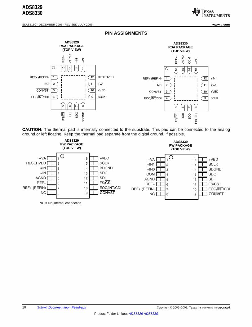
PIN ASSIGNMENTS
REF+ (REFIN)
NC
CONVST
EOC/ /CDIINT
RESERVED
+VA
+VBD
SCLK
1
2
3
4
12
11
10
9
RE
F-
16
FS
/ CS
5
AG
ND
15
SD
I6
-IN
14
SD
O7
+IN
13
BD
GN
D8
REF+ (REFIN)
NC
CONVST
EOC/ /CDIINT
+IN1
+VA
+VBD
SCLK
1
2
3
4
12
11
10
9
RE
F-
16
FS
/CS
5
AG
ND
15
SD
I6
CO
M14
SD
O7
+IN
013
BD
GN
D8
+VBD
SCLK
BDGND
SDO
SDI
FS/CS
EOC/INT/CDI
CONVST
+VA
RESERVED
+IN
-IN
AGND
REF-
REF+ (REFIN)
NC
1
2
3
4
5
6
7
8
16
15
14
13
12
11
10
9
+VBD
SCLK
BDGND
SDO
SDI
FS/CS
EOC/INT/CDI
CONVST
+VA
+IN1
+IN0
COM
AGND
REF-
REF+ (REFIN)
NC
1
2
3
4
5
6
7
8
16
15
14
13
12
11
10
9
ADS8329ADS8330
SLAS516C–DECEMBER 2006–REVISED JULY 2009 ................................................................................................................................................... www.ti.com
ADS8329 ADS8330RSA PACKAGE RSA PACKAGE
(TOP VIEW) (TOP VIEW)
CAUTION: The thermal pad is internally connected to the substrate. This pad can be connected to the analogground or left floating. Keep the thermal pad separate from the digital ground, if possible.
ADS8329 ADS8330PW PACKAGE PW PACKAGE
(TOP VIEW) (TOP VIEW)
NC = No internal connection
10 Submit Documentation Feedback Copyright © 2006–2009, Texas Instruments Incorporated
Product Folder Link(s): ADS8329 ADS8330

ADS8329ADS8330
www.ti.com ................................................................................................................................................... SLAS516C–DECEMBER 2006–REVISED JULY 2009
ADS8329 Terminal FunctionsNO.
NAME QFN TSSOP I/O DESCRIPTIONAGND 15 5 — Analog groundBDGND 8 14 — Interface groundCONVST 3 9 I Freezes sample and hold, starts conversion with next rising edge of internal clock
Status output. If programmed as EOC, this pin is low (default) when a conversion is inprogress. If programmed as an interrupt (INT), this pin is low for a preprogrammed
EOC/ INT/ CDI 4 10 O duration after the end of conversion and valid data are to be output. The polarity ofEOC or INT is programmable. This pin can also be used as a chain data input whenthe device is operated in chain mode.
5 11 I Frame sync signal for TMS320 DSP serial interface or chip select input for SPIFS/CS interface slave select (SS–).+IN 13 3 I Noninverting input–IN 14 4 I Inverting input, usually connected to groundNC 2 8 — No connection.REF+ 1 7 I External reference input.REF– 16 6 I Connect to AGND through individual via.RESERVED 12 2 I Connect to AGND or +VASCLK 9 15 I Clock for serial interfaceSDI 6 12 I Serial data inSDO 7 13 O Serial data out+VA 11 1 Analog supply, +2.7 V to +5.5 VDC.+VBD 10 16 Interface supply
ADS8330 Terminal FunctionsNO.
NAME QFN TSSOP I/O DESCRIPTIONAGND 15 5 — Analog groundBDGND 8 14 — Interface groundCOM 14 4 I Common inverting input, usually connected to groundCONVST 3 9 I Freezes sample and hold, starts conversion with next rising edge of internal clock
Status output. If programmed as EOC, this pin is low (default) when a conversion is inprogress. If programmed as an interrupt (INT), this pin is low for a preprogrammed
EOC/ INT/ CDI 4 10 O duration after the end of conversion and valid data are to be output. The polarity ofEOC or INT is programmable. This pin can also be used as a chain data input whenthe device is operated in chain mode.
5 11 I Frame sync signal for TMS320 DSP serial interface or chip select input for SPIFS/CS interface+IN1 12 2 I Second noninverting input.+IN0 13 3 I First noninverting inputNC 2 8 — No connection.REF+ 1 7 I External reference input.REF– 16 6 I Connect to AGND through individual via.SCLK 9 15 I Clock for serial interfaceSDI 6 12 I Serial data in (conversion start and reset possible)SDO 7 13 O Serial data out+VA 11 1 Analog supply, +2.7 V to +5.5 VDC.+VBD 10 16 Interface supply
Copyright © 2006–2009, Texas Instruments Incorporated Submit Documentation Feedback 11
Product Folder Link(s): ADS8329 ADS8330

tSAMPLE1 = 3 CCLKs min
td(CSR-EOS) = 20 ns min
tCONV = 18 CCLKs
th(CSF-EOC) th(CSF-EOC)
th(CSR-EOS)
th(CSF-EOS) tsu(CSF-EOC)tsu(CSF-EOS)
tSAMPLE1 = 3 CCLKs min
twL(CONVST)
EOC(active low)
MANUAL TRIGGER / READ While Sampling(use internal CCLK, EOC and polarity programmed as active low)INT
(active low)INT
/FSCS
SCLK
SDO
SDI
CONVST
Nth
Nth
EO
C
EO
S
EO
C
EO
S
1101b1101b
Nth−1st Nth
READ Result READ Result
1 . . . . . . . . . . . . . . . . . . . . 16
1
1101b
EO
S
EO
C
EO
S
EO
C
EO
S
1110b. . . . . . . . . . . . . . 1101b
Nth
CONFIGURE READ Result
N − 2nd N − 1st Nth
READ Result
EOC(active low)
AUTO TRIGGER / READ While Sampling(use internal CCLK, EOC and polarity programmed as active low)INT
(active low)INT
/FSCS
SCLK
SDO
SDI
= 1CONVST
tSAMPLE2 = 3 CCLKs tSAMPLE2 = 3 CCLKstCONV = 18 CCLKs tCONV = 18 CCLKs
th(CSF-EOC)
th(CSF-EOC)
th(CSF-EOS)
tsu(CSF-EOS)tsu(CSF-EOS)
1 . . . . . . . . . . . . . . . . . . .161 . . . . . . . . . . . . . . . . . . .16 1
ADS8329ADS8330
SLAS516C–DECEMBER 2006–REVISED JULY 2009 ................................................................................................................................................... www.ti.com
Figure 1. Timing for Conversion and Acquisition Cycles for Manual Trigger (Read while sampling)
Figure 2. Timing for Conversion and Acquisition Cycles for Autotrigger (Read while sampling)
12 Submit Documentation Feedback Copyright © 2006–2009, Texas Instruments Incorporated
Product Folder Link(s): ADS8329 ADS8330
1101b 1101b
EO
C
EO
S
EO
S
N th
Nth N − 1st
Nth N + 1st
N − 1st
READ Result READ Result
EOC(active low)
MANUAL TRIGGER / READ While Converting(use internal CCLK, EOC and polarity programmed as active low)INT
(active low)INT
/FSCS
SCLK
SDO
SDI
CONVST
twL(CONVST)
tSAMPLE1 = 3 CCLKs mintCONV = 18 CCLKs
th(CSF-EOC)
th(CSF-EOS)
tsu(CSF-EOS)tsu(CSR-EOS)
tsu(CSF-EOC)
1 . . . . . . . . . . . . . . . . . . . .16 1
1 . . . . . . . . . . . . . . . . . . .16
EO
C
EO
S
EO
C
EO
S
EO
S
1110b . . . . . . . . . . . . . . .
??
1101b 1101b
N−1st NthN−2nd
READ Result READ ResultCONFIGURE
Nth
N + 1stEOC(active low)
AUTO TRIGGER / READ While Converting(use internal CCLK, EOC and polarity programmed as active low)INT
(active low)INT
/FSCS
SCLK
SDO
SDI
= 1CONVST
tCONV = 18 CCLKs
th(CSR-EOS)
tsu(CSF-EOS) th(CSF-EOS)
tSAMPLE2 = 3 CCLKs min
tCONV = 18 CCLKs
th(CSF-EOS) tsu(CSR-EOS)
tsu(CSR-EOS)
tSAMPLE2 = 3 CCLKs min
1 . . . . . . . . . . . . . . . . . . 16
1 . . . . . . . . . . . . . . . . . . 16
ADS8329ADS8330
www.ti.com ................................................................................................................................................... SLAS516C–DECEMBER 2006–REVISED JULY 2009
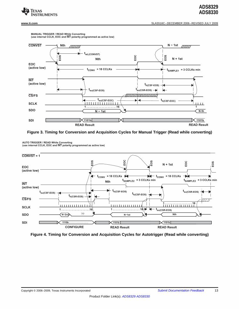
Figure 3. Timing for Conversion and Acquisition Cycles for Manual Trigger (Read while converting)
Figure 4. Timing for Conversion and Acquisition Cycles for Autotrigger (Read while converting)
Copyright © 2006–2009, Texas Instruments Incorporated Submit Documentation Feedback 13
Product Folder Link(s): ADS8329 ADS8330

1 2 3 54 6 7 15 1614
MSB−1 MSB−2 MSB−3 MSB−4 MSB−5 MSB−6 LSB+2 LSB+1 LSB
MSB−1 MSB−2 MSB−3 MSB−4 MSB−5 MSB−6 LSB+2 LSB+1 LSB
MSB
tsu(CSF−SCLK1F)
CS/FS
td(CSF−SDOVALID)
tsu(SDI−SCLKF)
th(SDI−SCLKF)
td(SCLKF−SDOINVALID)
td(SCLKF−SDOVALID)
td(CSR−SDOZ)
tsu(16thSCLK−CSR)twL(SCLK)
twH(SCLK)
tc(SCLK)
SCLK
SDO
SDI
Hi−Z
MSB
1101b1101b
MANUAL TRIGGER / READ While Sampling
(use internal CCLK , EOC and INTactive high active low, TAG enabled, auto channel select)
Hi−Z
EO
S
EO
C
READ Result READ Result
N−1st CH1
CONVST
INT(active low)
EOC(active low)
CS/FS
SCLK
SDO
SDI
Nth CH0
1 . . . . . . . . . . . . . . . . . . . . . . . 16 17 1 16. . . . . . . . . . . . . . . . . . . . . . . 17
Nth CH1
Nth CH1Nth CH0
Nth CH0Hi−Z
TAG = 0TAG = 1
twL(CONVST)
twL(CONVST)
tSAMPLE1 = 3 CCLKs min
tCONV = 18 CCLKs
td(CSR-EOS) = 20 ns MIN
tCONV = 18 CCLKs
th(CSF-EOC)
tsu(CSF-EOS)
ADS8329ADS8330
SLAS516C–DECEMBER 2006–REVISED JULY 2009 ................................................................................................................................................... www.ti.com
Figure 5. Detailed SPI Transfer Timing
Figure 6. Simplified Dual Channel Timing
14 Submit Documentation Feedback Copyright © 2006–2009, Texas Instruments Incorporated
Product Folder Link(s): ADS8329 ADS8330

TYPICAL CHARACTERISTICS
80
85
90
95
100
105
110
0 50 100 150 200
f - Frequency - kHz
Cro
ss
talk
-d
B
+VA = 5 V
+VA = 3 V
0
0.5
1
1.5
2
-40 -25 -10 5 20 35 50 65 80
T - Free-Air Temperature - °CA
INL
- L
SB
+VA = 5 V
+VA = 3 V
0
0.2
0.4
0.6
0.8
1
-40 -25 -10 5 20 35 50 65 80
T - Free-Air Temperature - °CA
DN
L-
LS
B +VA = 3 V
+VA = 5 V
-2
-1.5
-1
-0.5
0
0.5
1
1.5
2
0.1 1 10 100
External Clock Frequency - MHz
INL
- L
SB
MIN
MAX
+VA = 5 V
-1
-0.5
0
0.5
1
0.1 1 10 100
External Clock Frequency - MHz
DN
L-
LS
B
MAX
MIN
+VA = 5 V
-1
-0.5
0
0.5
1
0.1 1 10 100
External Clock Frequency - MHz
DN
L-
LS
B
MAX
MIN
+VA = 3 V
ADS8329ADS8330
www.ti.com ................................................................................................................................................... SLAS516C–DECEMBER 2006–REVISED JULY 2009
At –40°C to 85°C, VREF [REF+ – (REF–)] = 5 V when +VA = +VBD = 5 V or VREF [REF+ – (REF–)] = 2.5 V when+VA = +VBD = 3 V, fSCLK = 42 MHz, or VREF = 2.5 when +VA = +VBD = 2.7 V, fSCLK = 37.8 MHz, fI = dc for dccurves, fI = 100 kHz for ac curves with 5-V supply and fI = 10 kHz for ac curves with 3-V supply (unlessotherwise noted).
CROSSTALK DIFFERENTIAL NONLINEARITY INTEGRAL NONLINEARITYvs vs vs
FREQUENCY FREE-AIR TEMPERATURE FREE-AIR TEMPERATURE
Figure 7. Figure 8. Figure 9.
DIFFERENTIAL NONLINEARITY INTEGRAL NONLINEARITY DIFFERENTIAL NONLINEARITYvs vs vs
EXTERNAL CLOCK FREQUENCY EXTERNAL CLOCK FREQUENCY EXTERNAL CLOCK FREQUENCY
Figure 10. Figure 11. Figure 12.
Copyright © 2006–2009, Texas Instruments Incorporated Submit Documentation Feedback 15
Product Folder Link(s): ADS8329 ADS8330

-2
-1.5
-1
-0.5
0
0.5
1
1.5
2
0.1 1 10 100
External Clock Frequency - MHz
INL
- L
SB
MAX
MIN
+VA = 3 V
0
0.2
0.4
0.6
0.8
1
2.7 3.2 3.7 4.2 4.7 5.2
+VA - Supply Voltage - V
Off
se
t V
olt
ag
e -
mV
-1
-0.5
0
0.5
1
-40 -25 -10 5 20 35 50 65 80
T - Free-Air Temperature - °CA
Off
set
Vo
ltag
e -
mV +VA = 5 V
+VA = 3 V
-0.10
-0.05
0
0.05
0.10
2.7 3.2 3.7 4.2 4.7 5.2
+VA - Supply Voltage - V
Ga
in E
rro
r -
%F
SR
-70
-72
-74
-76
-78
-80
0 20 40 60 80 100
f - Frequency - kHz
PS
RR
- P
ow
er
Su
pp
ly R
eje
cti
on
Ra
tio
- d
B
+VA = 3 V
+VA = 5 V
-0.10
-0.08
-0.06
-0.04
-0.02
0
-40 -25 -10 5 20 35 50 65 80
T - Free-Air Temperature - °CA
Gain
Err
or
- %
FS
R
+VA = 5 V
+VA = 3 V
85
87
89
91
93
95
0 20 40 60 80 100
f - Input Frequency - kHzi
SN
R -
Sig
na
l-To
-No
ise
Ra
tio
- d
B
+VA = 5 V
+VA = 3 V
85
87
89
91
93
95
0 20 40 60 80 100
f - Input Frequency - kHzi
SIN
AD
- S
ign
al-
To
-No
ise a
nd
Dis
tort
ion
- d
B
+VA = 5 V
+VA = 3 V
-110
-105
-100
-95
-90
0 20 40 60 80 100
f - Input Frequency - kHzi
TH
D -
To
tal
Ha
rmo
nic
Dis
tort
ion
- d
B
+VA = 5 V
+VA = 3 V
ADS8329ADS8330
SLAS516C–DECEMBER 2006–REVISED JULY 2009 ................................................................................................................................................... www.ti.com
TYPICAL CHARACTERISTICS (continued)
INTEGRAL NONLINEARITY OFFSET VOLTAGE OFFSET VOLTAGEvs vs vs
EXTERNAL CLOCK FREQUENCY FREE-AIR TEMPERATURE SUPPLY VOLTAGE
Figure 13. Figure 14. Figure 15.
GAIN ERROR GAIN ERROR POWER-SUPPLY REJECTION RATIOvs vs vs
FREE-AIR TEMPERATURE SUPPLY VOLTAGE SUPPLY RIPPLE FREQUENCY
Figure 16. Figure 17. Figure 18.
SIGNAL-TO-NOISE RATIO SIGNAL-TO-NOISE AND DISTORTION TOTAL HARMONIC DISTORTIONvs vs vs
INPUT FREQUENCY INPUT FREQUENCY INPUT FREQUENCY
Figure 19. Figure 20. Figure 21.
16 Submit Documentation Feedback Copyright © 2006–2009, Texas Instruments Incorporated
Product Folder Link(s): ADS8329 ADS8330

70
75
80
85
90
95
100
0 1 2 3 4 5
Full Scale Range - V
SN
R -
Sig
na
l-To
-No
ise
Ra
tio
- d
B
+VA = 3 V
+VA = 5 V
f = 10 kHzi
70
75
80
85
90
95
100
0 1 2 3 4 5
Full Scale Range - V
SIN
AD
- S
ign
al-
To
-No
ise
an
d D
isto
rtio
n -
dB
+VA = 3 V
+VA = 5 V
f = 10 kHzi
90
92
94
96
98
100
102
104
106
108
110
0 20 40 60 80 100
f - Input Frequency - kHzi
SF
DR
- S
pu
rio
us F
ree D
yn
am
ic R
an
ge -
dB
+VA = 5 V
+VA = 3 V
-110
-105
-100
-95
-90
-85
-80
0 1 2 3 4 5
Full Scale Range - V
TH
D -
To
tal
Ha
rmo
nic
Dis
tort
ion
- d
B
+VA = 5 V
+VA = 3 V
f = 10 kHzi
80
85
90
95
100
105
110
0 1 2 3 4 5
Full Scale Range - V
SF
DR
- S
pu
rio
us F
ree D
yn
am
ic R
an
ge -
dB
+VA = 3 V
+VA = 5 V
f = 10 kHzi
-110
-105
-100
-95
-90
-40 -25 -10 5 20 35 50 65 80
T - Free-Air Temperature - °CA
TH
D -
To
tal
Ha
rmo
nic
Dis
tort
ion
- d
B
+VA = 5 V
+VA = 3 V
90
95
100
105
110
-40 -25 -10 5 20 35 50 65 80
T - Free-Air Temperature - °CA
SF
DR
- S
pu
rio
us
Fre
e D
yn
am
ic R
an
ge
- d
B
+VA = 5 V
+VA = 3 V
85
87
89
91
93
95
-40 -25 -10 5 20 35 50 65 80
T - Free-Air Temperature - ºCA
SN
R -
Sig
nal-
To
-No
ise R
ati
o -
dB
+VA = 5 V
+VA = 3 V
85
87
89
91
93
95
-40 -25 -10 5 20 35 50 65 80
T - Free-Air Temperature - ºCA
SIN
AD
- S
ign
al-
To
-No
ise
an
d D
isto
rtio
n -
dB
+VA = 5 V
+VA = 3 V
ADS8329ADS8330
www.ti.com ................................................................................................................................................... SLAS516C–DECEMBER 2006–REVISED JULY 2009
TYPICAL CHARACTERISTICS (continued)
SPURIOUS-FREE DYNAMIC RANGE SIGNAL-TO-NOISE RATIO SIGNAL-TO-NOISE AND DISTORTIONvs vs vs
INPUT FREQUENCY FULL-SCALE RANGE FULL-SCALE RANGE
Figure 22. Figure 23. Figure 24.
TOTAL HARMONIC DISTORTION SPURIOUS-FREE DYNAMIC RANGE TOTAL HARMONIC DISTORTIONvs vs vs
FULL-SCALE RANGE FULL-SCALE RANGE FREE-AIR TEMPERATURE
Figure 25. Figure 26. Figure 27.
SPURIOUS-FREE DYNAMIC RANGE SIGNAL-TO-NOISE RATIO SIGNAL-TO-NOISE AND DISTORTIONvs vs vs
FREE-AIR TEMPERATURE FREE-AIR TEMPERATURE FREE-AIR TEMPERATURE
Figure 28. Figure 29. Figure 30.
Copyright © 2006–2009, Texas Instruments Incorporated Submit Documentation Feedback 17
Product Folder Link(s): ADS8329 ADS8330

21
21.5
22
22.5
23
23.5
24
2.7 3.2 3.7 4.2 4.7 5.2
+VA - Supply Voltage - V
Inte
rna
l C
lock F
req
uen
cy
- M
Hz
14
14.50
15
15.50
16
-40 -25 -10 5 20 35 50 65 80
EN
OB
- E
ffecti
ve N
um
ber
of
Bit
s -
Bit
s
T - Free-Air Temperature - ºCA
+VA = 5 V
+VA = 3 V
21
21.5
22
22.5
23
23.5
24
-40 -25 -10 5 20 35 50 65 80
T - Free-Air Temperature - ºCA
Inte
rnal C
lock F
req
uen
cy -
MH
z
4.5
5.0
5.5
6.0
6.5
7.0
7.5
2.7 3.2 3.7 4.2 4.7 5.2
+VA - Supply Voltage - V
An
alo
g S
up
ply
Cu
rren
t -
mA
f = 1 MSPSs
200
240
280
320
360
400
2.7 3.2 3.7 4.2 4.7 5.2
+VA - Supply Voltage - V
An
alo
g S
up
ply
Cu
rren
t -
Am
NAP Mode
0
2
4
6
8
10
2.7 3.2 3.7 4.2 4.7 5.2
An
alo
g S
up
ply
Cu
rre
nt
- n
A
+VA - Supply Voltage - V
PD Mode
0
1
2
3
4
5
6
7
1 10 100 1000
Sample Rate - kHz
An
alo
g S
up
ply
Cu
rren
t -
mA
+VA = 3 V
+VA = 5 V
Auto NAP
0
100
200
300
400
500
1 5 9 13 17
Sample Rate - kHz
An
alo
g S
up
ply
Cu
rre
nt
-A
m
+VA = 5 V
+VA = 3 V
PD Mode
4
4.5
5
5.5
6
6.5
7
7.5
-40 -25 -10 5 20 35 50 65 80
An
alo
g S
up
ply
Cu
rre
nt
- m
A
T - Free-Air Temperature - ºCA
+VA = 5 V
+VA = 3 V
f = 1 MSPSs
ADS8329ADS8330
SLAS516C–DECEMBER 2006–REVISED JULY 2009 ................................................................................................................................................... www.ti.com
TYPICAL CHARACTERISTICS (continued)
EFFECTIVE NUMBER OF BITS INTERNAL CLOCK FREQUENCY INTERNAL CLOCK FREQUENCYvs vs vs
FREE-AIR TEMPERATURE SUPPLY VOLTAGE FREE-AIR TEMPERATURE
Figure 31. Figure 32. Figure 33.
ANALOG SUPPLY CURRENT ANALOG SUPPLY CURRENT ANALOG SUPPLY CURRENTvs vs vs
SUPPLY VOLTAGE SUPPLY VOLTAGE SUPPLY VOLTAGE
Figure 34. Figure 35. Figure 36.
ANALOG SUPPLY CURRENT ANALOG SUPPLY CURRENT ANALOG SUPPLY CURRENTvs vs vs
SAMPLE RATE SAMPLE RATE FREE-AIR TEMPERATURE
Figure 37. Figure 38. Figure 39.
18 Submit Documentation Feedback Copyright © 2006–2009, Texas Instruments Incorporated
Product Folder Link(s): ADS8329 ADS8330

0.2
0.24
0.28
0.32
0.36
0.4
-40 -25 -10 5 20 35 50 65 80
An
alo
g S
up
ply
Cu
rre
nt
- m
A
T - Free-Air Temperature - ºCA
+VA = 5 V
+VA = 3 V
NAP Mode
0 10000 20000 30000 40000 50000 60000
Code
+VA = 5 V
INL
-1.75
-0.5
0
0.5
1.75
INL
- B
its
1.0
-1.0
1.5
-1.5
-1
-0.5
0
0.5
1
0 10000 20000 30000 40000 50000 60000
Code
DN
L-
Bit
s
DNL
+VA = 5 V
ADS8329ADS8330
www.ti.com ................................................................................................................................................... SLAS516C–DECEMBER 2006–REVISED JULY 2009
TYPICAL CHARACTERISTICS (continued)
ANALOG SUPPLY CURRENTvs
FREE-AIR TEMPERATURE
Figure 40.
Figure 41.
Figure 42.
Copyright © 2006–2009, Texas Instruments Incorporated Submit Documentation Feedback 19
Product Folder Link(s): ADS8329 ADS8330

-1.75
-0.5
0
0.5
1.75
0 10000 20000 30000 40000 50000 60000
Code
INL
INL
- B
its
+VA = 3 V
1.0
-1.0
1.5
-1.5
-1
-0.5
0
0.5
1
0 10000 20000 30000 40000 50000 60000
Code
DNL
DN
L-
Bit
s
+VA = 3 V
FFT
-160
-140
-120
-100
-80
-60
-40
-20
0
0 100 200 300 400 500
f - Frequency - kHz
Am
plitu
de -
dB
5 kHz Input,
+VA = 3 V,
f = 1 MSPS,
V = 2.5 V
s
ref
ADS8329ADS8330
SLAS516C–DECEMBER 2006–REVISED JULY 2009 ................................................................................................................................................... www.ti.com
TYPICAL CHARACTERISTICS (continued)
Figure 43.
Figure 44.
Figure 45.
20 Submit Documentation Feedback Copyright © 2006–2009, Texas Instruments Incorporated
Product Folder Link(s): ADS8329 ADS8330

FFT
-160
-140
-120
-100
-80
-60
-40
-20
0
0 100 200 300 400 500
f - Frequency - kHz
Am
pli
tud
e -
dB
10 kHz Input,
+VA = 3 V,
f = 1 MSPS,
V = 2.5 V
s
ref
FFT
-160
-140
-120
-100
-80
-60
-40
-20
0
0 100 200 300 400 500
f - Frequency - kHz
Am
pli
tud
e -
dB
100 kHz Input,
+VA = 3 V,
f = 1 MSPS,
V = 2.5 V
s
ref
FFT
-160
-140
-120
-100
-80
-60
-40
-20
0
0 100 200 300 400 500
f - Frequency - kHz
Am
pli
tud
e -
dB
5 kHz Input,
+VA = 5 V,
f = 1 MSPS,
V = 5 V
s
ref
ADS8329ADS8330
www.ti.com ................................................................................................................................................... SLAS516C–DECEMBER 2006–REVISED JULY 2009
TYPICAL CHARACTERISTICS (continued)
Figure 46.
Figure 47.
Figure 48.
Copyright © 2006–2009, Texas Instruments Incorporated Submit Documentation Feedback 21
Product Folder Link(s): ADS8329 ADS8330
FFT
-160
-140
-120
-100
-80
-60
-40
-20
0
20
0 100 200 300 400 500
f - Frequency - kHz
Am
pli
tud
e -
dB
10 kHz Input,
+VA = 5 V,
f = 1 MSPS,
V = 5 V
s
ref
FFT
-160
-140
-120
-100
-80
-60
-40
-20
0
0 100 200 300 400 500
f - Frequency - kHz
Am
plitu
de -
dB
100 kHz Input,
+VA = 5 V,
f = 1 MSPS,
V = 5 V
s
ref
THEORY OF OPERATION
ANALOG INPUT
ADS8329ADS8330
SLAS516C–DECEMBER 2006–REVISED JULY 2009 ................................................................................................................................................... www.ti.com
TYPICAL CHARACTERISTICS (continued)
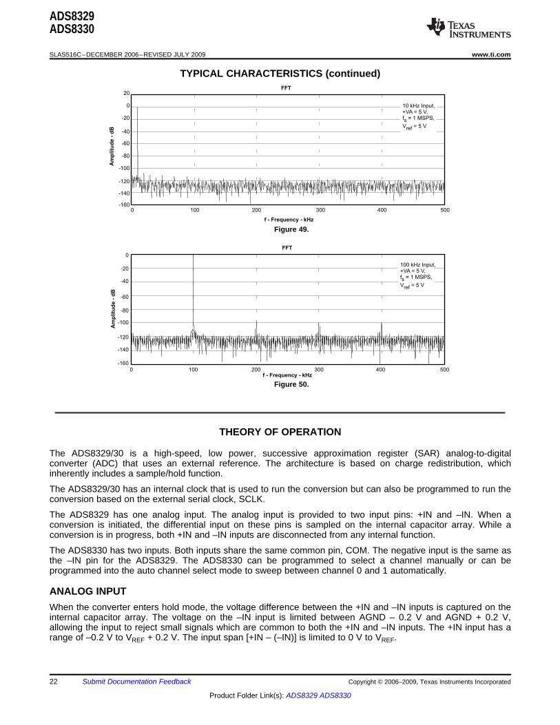
Figure 49.
Figure 50.
The ADS8329/30 is a high-speed, low power, successive approximation register (SAR) analog-to-digitalconverter (ADC) that uses an external reference. The architecture is based on charge redistribution, whichinherently includes a sample/hold function.
The ADS8329/30 has an internal clock that is used to run the conversion but can also be programmed to run theconversion based on the external serial clock, SCLK.
The ADS8329 has one analog input. The analog input is provided to two input pins: +IN and –IN. When aconversion is initiated, the differential input on these pins is sampled on the internal capacitor array. While aconversion is in progress, both +IN and –IN inputs are disconnected from any internal function.
The ADS8330 has two inputs. Both inputs share the same common pin, COM. The negative input is the same asthe –IN pin for the ADS8329. The ADS8330 can be programmed to select a channel manually or can beprogrammed into the auto channel select mode to sweep between channel 0 and 1 automatically.
When the converter enters hold mode, the voltage difference between the +IN and –IN inputs is captured on theinternal capacitor array. The voltage on the –IN input is limited between AGND – 0.2 V and AGND + 0.2 V,allowing the input to reject small signals which are common to both the +IN and –IN inputs. The +IN input has arange of –0.2 V to VREF + 0.2 V. The input span [+IN – (–IN)] is limited to 0 V to VREF.
22 Submit Documentation Feedback Copyright © 2006–2009, Texas Instruments Incorporated
Product Folder Link(s): ADS8329 ADS8330

Device in Hold Mode
AGND150
+IN
−IN AGND
+VA
150
4 pF
4 pF
40 pF
40 pF
Driver Amplifier Choice
Bipolar to Unipolar Driver
ADS8329ADS8330
www.ti.com ................................................................................................................................................... SLAS516C–DECEMBER 2006–REVISED JULY 2009
The (peak) input current through the analog inputs depends upon a number of factors: sample rate, inputvoltage, and source impedance. The current into the ADS8329/30 charges the internal capacitor array during thesample period. After this capacitance has been fully charged, there is no further input current. The source of theanalog input voltage must be able to charge the input capacitance (45 pF) to a 16-bit settling level within theminimum acquisition time (120 ns). When the converter goes into hold mode, the input impedance is greater than1 GΩ.
Care must be taken regarding the absolute analog input voltage. To maintain linearity of the converter, the +INand –IN inputs and the span [+IN – (–IN)] should be within the limits specified. Outside of these ranges,converter linearity may not meet specifications. To minimize noise, low bandwidth input signals with low-passfilters should be used. Care should be taken to ensure that the output impedance of the sources driving the +INand –IN inputs are matched. If this is not observed, the two inputs could have different settling times. This mayresult in an offset error, gain error, and linearity error which change with temperature and input voltage.
Figure 51. Input Equivalent Circuit
The analog input to the converter needs to be driven with a low noise, op-amp like the THS4031 or OPA365. AnRC filter is recommended at the input pins to low-pass filter the noise from the source. Two resistors of 20 Ω anda capacitor of 470 pF are recommended. The input to the converter is a unipolar input voltage in the range 0 V toVREF. The minimum –3dB bandwidth of the driving operational amplifier can be calculated to:
f3db = (ln(2) ×(n+1))/(2π × tACQ)
where n is equal to 16, the resolution of the ADC (in the case of the ADS8329/30). When tACQ = 120 ns(minimum acquisition time), the minimum bandwidth of the driving amplifier is 15.6 MHz. The bandwidth can berelaxed if the acquisition time is increased by the application. The OPA365, OPA827, or THS4031 from TexasInstruments are recommended. The THS4031 used in the source follower configuration to drive the converter isshown in the typical input drive configuration, Figure 52. For the ADS8330, a series resistor of 0Ω should beused on the COM pin (or no resistor at all).
In systems where the input is bipolar, the THS4031 can be used in the inverting configuration with an additionalDC bias applied to its + input so as to keep the input to the ADS8329/30 within its rated operating voltage range.This configuration is also recommended when the ADS8329/30 is used in signal processing applications wheregood SNR and THD performance is required. The DC bias can be derived from the REF3225 or the REF3240reference voltage ICs. The input configuration shown in Figure 53 is capable of delivering better than 91 dB SNRand –96 dB THD at an input frequency of 10 kHz. In case bandpass filters are used to filter the input, care shouldbe taken to ensure that the signal swing at the input of the bandpass filter is small so as to keep the distortionintroduced by the filter minimal. In such cases, the gain of the circuit shown in Figure 53 can be increased tokeep the input to the ADS8329/30 large to keep the SNR of the system high. Note that the gain of the systemfrom the + input to the output of the THS4031 in such a configuration is a function of the gain of the AC signal. Aresistor divider can be used to scale the output of the REF3225 or REF3240 to reduce the voltage at the DCinput to THS4031 to keep the voltage at the input of the converter within its rated operating range.
Copyright © 2006–2009, Texas Instruments Incorporated Submit Documentation Feedback 23
Product Folder Link(s): ADS8329 ADS8330

ADS8329
+IN
-IN
THS403120 W
20 W
470 pF
50 W
Input
Signal
(0 V to 4 V)
5 V
+VA
ADS8329
+IN
-IN
THS403120 W
20 W
1V DC
InputSignal
(-2 V to 2 V)
5 V
+VA
470 pF600 W
600 W
REFERENCE
CONVERTER OPERATION
ADS8329ADS8330
SLAS516C–DECEMBER 2006–REVISED JULY 2009 ................................................................................................................................................... www.ti.com
Figure 52. Unipolar Input Drive Configuration
Figure 53. Bipolar Input Drive Configuration
The ADS8329/30 can operate with an external reference with a range from 0.3 V to 5 V. A clean, low noise,well-decoupled reference voltage on this pin is required to ensure good performance of the converter. A lownoise band-gap reference like the REF3240 can be used to drive this pin. A 22-µF ceramic decoupling capacitoris required between the REF+ and REF– pins of the converter. These capacitors should be placed as close aspossible to the pins of the device. The REF– should be connected to its own via to the analog ground plane withthe shortest possible distance.
The ADS8329/30 has an oscillator that is used as an internal clock which controls the conversion rate. Thefrequency of this clock is 21 MHz minimum. The oscillator is always on unless the device is in the deeppower-down state or the device is programmed for using SCLK as the conversion clock (CCLK). The minimumacquisition (sampling) time takes 3 CCLKs (this is equivalent to 120 ns at 24.5 MHz) and the conversion timetakes 18 conversion clocks (CCLK) (≈780 ns) to complete one conversion.
The conversion can also be programmed to run based on the external serial clock, SCLK, if is so desired. Thisallows a system designer to achieve system synchronization. The serial clock SCLK, is first reduced to 1/2 of itsfrequency before it is used as the conversion clock (CCLK). For example, with a 42-MHz SCLK this provides a21-MHz clock for conversions. If it is desired to start a conversion at a specific rising edge of the SCLK when theexternal SCLK is programmed as the source of the conversion clock (CCLK) (and manual start of conversion isselected), the setup time between CONVST and that rising SCLK edge should be observed. This ensures theconversion is complete in 18 CCLKs (or 36 SCLKs). The minimum setup time is 20 ns to ensure synchronizationbetween CONVST and SCLK. In many cases the conversion can start one SCLK period (or CCLK) later whichresults in a 19 CCLK (or 37 SCLK) conversion. The 20 ns setup time is not required once synchronization isrelaxed.
24 Submit Documentation Feedback Copyright © 2006–2009, Texas Instruments Incorporated
Product Folder Link(s): ADS8329 ADS8330
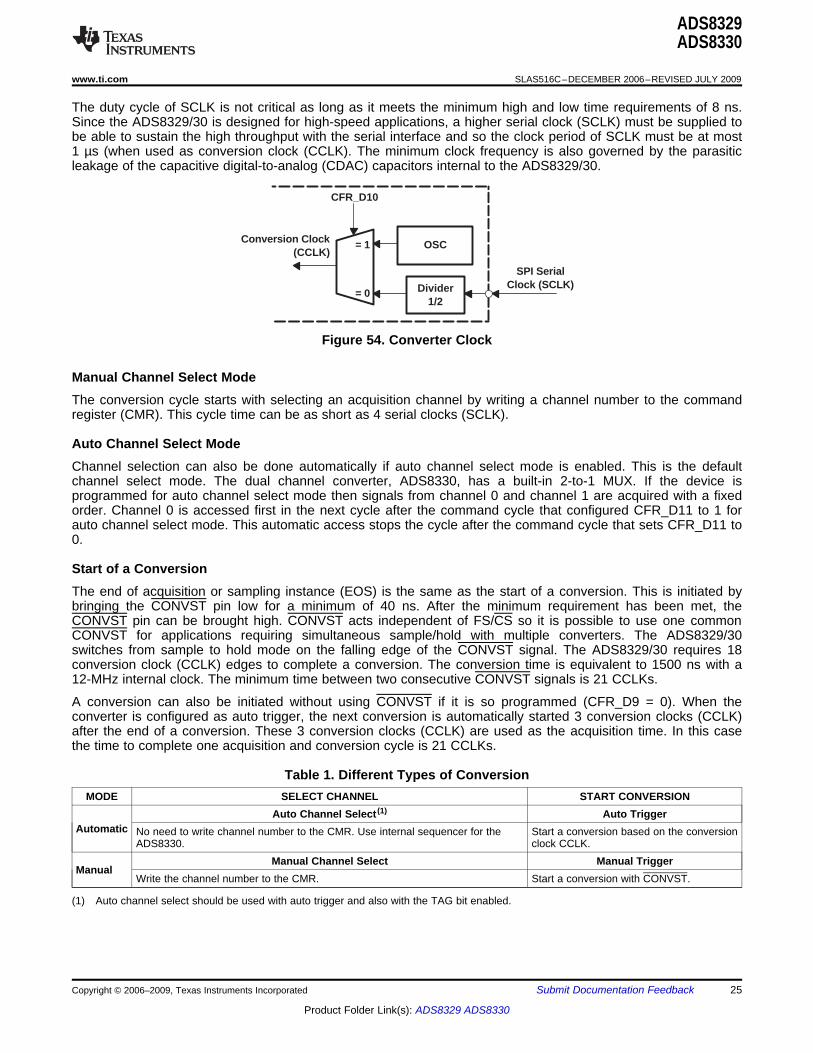
OSC
Divider1/2
= 1
= 0
Conversion Clock(CCLK)
CFR_D10
SPI SerialClock (SCLK)
Manual Channel Select Mode
Auto Channel Select Mode
Start of a Conversion
ADS8329ADS8330
www.ti.com ................................................................................................................................................... SLAS516C–DECEMBER 2006–REVISED JULY 2009
The duty cycle of SCLK is not critical as long as it meets the minimum high and low time requirements of 8 ns.Since the ADS8329/30 is designed for high-speed applications, a higher serial clock (SCLK) must be supplied tobe able to sustain the high throughput with the serial interface and so the clock period of SCLK must be at most1 µs (when used as conversion clock (CCLK). The minimum clock frequency is also governed by the parasiticleakage of the capacitive digital-to-analog (CDAC) capacitors internal to the ADS8329/30.
Figure 54. Converter Clock
The conversion cycle starts with selecting an acquisition channel by writing a channel number to the commandregister (CMR). This cycle time can be as short as 4 serial clocks (SCLK).
Channel selection can also be done automatically if auto channel select mode is enabled. This is the defaultchannel select mode. The dual channel converter, ADS8330, has a built-in 2-to-1 MUX. If the device isprogrammed for auto channel select mode then signals from channel 0 and channel 1 are acquired with a fixedorder. Channel 0 is accessed first in the next cycle after the command cycle that configured CFR_D11 to 1 forauto channel select mode. This automatic access stops the cycle after the command cycle that sets CFR_D11 to0.
The end of acquisition or sampling instance (EOS) is the same as the start of a conversion. This is initiated bybringing the CONVST pin low for a minimum of 40 ns. After the minimum requirement has been met, theCONVST pin can be brought high. CONVST acts independent of FS/CS so it is possible to use one commonCONVST for applications requiring simultaneous sample/hold with multiple converters. The ADS8329/30switches from sample to hold mode on the falling edge of the CONVST signal. The ADS8329/30 requires 18conversion clock (CCLK) edges to complete a conversion. The conversion time is equivalent to 1500 ns with a12-MHz internal clock. The minimum time between two consecutive CONVST signals is 21 CCLKs.
A conversion can also be initiated without using CONVST if it is so programmed (CFR_D9 = 0). When theconverter is configured as auto trigger, the next conversion is automatically started 3 conversion clocks (CCLK)after the end of a conversion. These 3 conversion clocks (CCLK) are used as the acquisition time. In this casethe time to complete one acquisition and conversion cycle is 21 CCLKs.
Table 1. Different Types of ConversionMODE SELECT CHANNEL START CONVERSION
Auto Channel Select (1) Auto TriggerAutomatic No need to write channel number to the CMR. Use internal sequencer for the Start a conversion based on the conversion
ADS8330. clock CCLK.Manual Channel Select Manual Trigger
ManualWrite the channel number to the CMR. Start a conversion with CONVST.
(1) Auto channel select should be used with auto trigger and also with the TAG bit enabled.
Copyright © 2006–2009, Texas Instruments Incorporated Submit Documentation Feedback 25
Product Folder Link(s): ADS8329 ADS8330

Status Output EOC/INT
Power-Down Modes
0.1
1
10
100
20 10020 20020 30020 40020
Settling T ime − ns
+VA
− S
uppl
y C
urre
nt −
A
ADS8329ADS8330
SLAS516C–DECEMBER 2006–REVISED JULY 2009 ................................................................................................................................................... www.ti.com
When the status pin is programmed as EOC and the polarity is set as active low, the pin works in the followingmanner: The EOC output goes LOW immediately following CONVST going LOW when manual trigger isprogrammed. EOC stays LOW throughout the conversion process and returns to HIGH when the conversion hasended. The EOC output goes low for 3 conversion clocks (CCLK) after the previous rising edge of EOC, if autotrigger is programmed.
This status pin is programmable. It can be used as an EOC output (CFR_D[7:6] = 1, 1) where the low time isequal to the conversion time. This status pin can be used as INT. (CFR_D[7:6] = 1, 0) which is set LOW at theend of a conversion is brought to HIGH (cleared) by the next read cycle. The polarity of this pin, used as eitherfunction (EOC or INT), is programmable through CFR_D7.
The ADS8329/30 has a comprehensive built-in power-down feature. There are three power-down modes: Deeppower-down mode, Nap power-down mode, and auto nap power-down mode. All three power-down modes areenabled by setting the related CFR bits. The first two power-down modes are activated when enabled. A wakeupcommand, 1011b, can resume device operation from a power-down mode. Auto nap power-down mode worksslightly different. When the converter is enabled in auto nap power-down mode, an end of conversion instance(EOC) puts the device into auto nap power-down. The beginning of sampling resumes operation of the converter.The contents of the configuration register is not affected by any of the power-down modes. Any ongoingconversion when nap or deep power-down is activated is aborted.
Figure 55. Typical Analog Supply Current Drop vs Time After Power-Down
26 Submit Documentation Feedback Copyright © 2006–2009, Texas Instruments Incorporated
Product Folder Link(s): ADS8329 ADS8330

ADS8329ADS8330
www.ti.com ................................................................................................................................................... SLAS516C–DECEMBER 2006–REVISED JULY 2009
Deep Power-Down ModeDeep power-down mode can be activated by writing to configuration register bit CFR_D2. When the device is indeep power-down mode, all blocks except the interface are in power-down. The external SCLK is blocked to theanalog block. The analog blocks no longer have bias currents and the internal oscillator is turned off. In thismode, supply current falls from 7 mA to 4 nA in 100 ns. The wake-up time after a power-down is 1 µs. When bitD2 in the configuration register is set to 0, the device is in deep power-down. Setting this bit to 1 or sending awake-up command can resume the converter from the deep power-down state.
Nap ModeIn nap mode the ADS8329/230 turns off biasing of the comparator and the mid-volt buffer. In this mode supplycurrent falls from 7 mA in normal mode to about 0.3 mA in 200 ns after the configuration cycle. The wake-up(resume) time from nap power-down mode is 3 CCLKs (120 ns with a 24.5-MHz conversion clock). As soon asthe CFR_D3 bit in the control register is set to 0, the device goes into nap power-down mode, regardless of theconversion state. Setting this bit to 1 or sending a wake-up command can resume the converter from the nappower-down state.
Auto Nap ModeAuto nap mode is almost identical to nap mode. The only difference is the time when the device is actuallypowered down and the method to wake up the device. Configuration register bit D4 is only used toenable/disable auto nap mode. If auto nap mode is enabled, the device turns off biasing after the conversion hasfinished, which means the end of conversion activates auto nap power-down mode. Supply current falls from 7mA in normal mode to about 0.3 mA in 200 ns. A CONVST resumes the device and turns biasing on again in 3CCLKs (120 ns with a 24.5-MHz conversion clock). The device can also be woken up by disabling auto napmode when bit D4 of the configuration register is set to 1. Any channel select command 0XXXb, wake upcommand or the set default mode command 1111b can also wake up the device from auto nap power-down.
NOTE:1. This wake-up command is the word 1011b in the command word. This command sets bits
D2 and D3 to 1 in the configuration register but not D4. But a wake-up command doesremove the device from either one of these power-down states, deep/nap/auto nappower-down.
2. Wake-up time is defined as the time between when the host processor tries to wake up theconverter and when a convert start can occur.
Table 2. Power-Down Mode ComparisonsPOWER
TYPE OF CONSUMPTION: RESUMEPOWER-DOWN 5 V/3 V ACTIVATED BY ACTIVATION TIME RESUME POWER BY TIME ENABLE
Normal operation 7 mA/5.1 mA
Deep power-down 4 nA/2 nA Setting CFR 100 ns Woken up by command 1011b 1 µs Set CFR
Woken up by command 1011b toNap power-down 0.3 mA/0.25 mA Setting CFR 200 ns 3 CCLKs Set CFRachieve 6.6 mA since (1.3 + 12)/2 = 6.6
Woken up by CONVST, any channelAuto nap EOC (end of 200 ns select command, default command 3 CCLKs Set CFRpower-down conversion) 1111b, or wake up command 1011b.
Copyright © 2006–2009, Texas Instruments Incorporated Submit Documentation Feedback 27
Product Folder Link(s): ADS8329 ADS8330

N N+1
ConverterState
EO
C
EO
S
EO
S
EO
C
Read N−1 −th Result
Read N −th Result
N −th Conversion N+1 −th ConversionN+1 −th Sampling
20 ns MIN
Converter State
0 ns MIN
CS
CS
CONVST
Read While Converting
Read While Sampling
(For Read Result)
(For Read Result)
20 ns MIN
1 CCLK MIN
N N+1Manual Trigger
ConverterState
EO
C
EO
S
EO
C
EO
S
Read N−1 −th
Result
20 ns MIN
Read N −thResult
20 ns MIN
Read N−1 −th
Result
20 ns MIN
Read N −thResult
20 ns MIN
Resume ActivationN −th Sampling
>=3CCLK
N −th Conversion
=18 CCLK
Resume ActivationN+1 −th Sampling
>=3CCLK
N+1 −th Conversion
=18 CCLK
CS
CS
CONVST
Read While Converting
Read While Sampling0 ns MIN
1 CCLK MIN
20 ns MIN
20 ns MIN20 ns MIN
20 ns MIN
ADS8329ADS8330
SLAS516C–DECEMBER 2006–REVISED JULY 2009 ................................................................................................................................................... www.ti.com
Figure 56. Read While Converting versus Read While Sampling (Manual Trigger)
Figure 57. Read While Converting versus Read While Sampling with Deep or Nap Power-Down
28 Submit Documentation Feedback Copyright © 2006–2009, Texas Instruments Incorporated
Product Folder Link(s): ADS8329 ADS8330

N N+1
Manual Trigger Case 1
EO
S
EO
C
EO
S
EOC(programmed
Active Low)
ConverterState
Resume N −th Sampling
>=3CCLK
EO
C
EO
S
N −th Conversion
=18 CCLK
Resume N+1 −th Sampling
>=3CCLK
EO
C
EO
S
N+1 −th Conversion
=18 CCLK
Read N−1 −thResult
20 ns MIN
Read N −thResult
20 ns MIN
Read N−1 −thResult
1 CCLK MIN
Read N −thResult
1 CCLK MIN
ConverterState
Resume N −th Sampling
>=3CCLK
EO
C
N −th Conversion
=18 CCLK
Resume N+1 −th Sampling
>=3CCLK
N+1 −th Conversion
=18 CCLK
Read N−1 −thResult
20 ns MIN
Read N −thResult
20 ns MIN
Read N−1 −thResult
20 ns MIN
Read N −thResult
20 ns MIN
40 ns MIN
EOC(programmed
Active Low)
N N+1
40 ns MIN
POWERDOWN POWERDOWN
CONVST
CS
Read While Converting
0 ns MIN
CONVST
CS
Read While Sampling
POWERDOWN
POWERDOWN
CS
Read While Converting
Read While Sampling
CS
0 ns MIN
Manual Trigger Case 2 (wake up by CONVST)
6 CCLKs 6 CCLKs
20 ns MIN 20 ns MIN
20 ns MIN20 ns MIN
20 ns MIN 20 ns MIN
20 ns MIN20 ns MIN
ADS8329ADS8330
www.ti.com ................................................................................................................................................... SLAS516C–DECEMBER 2006–REVISED JULY 2009
Figure 58. Read While Converting versus Read While Sampling with Auto Nap Power-Down
Total Acquisition + Conversion Cycle Time:Automatic: = 21 CCLKsManual: ≥ 21 CCLKsManual + deep ≥ 4SCLK + 100 µs + 3 CCLK + 18 CCLK +16 SCLK + 1 µspower-down:Manual + nap power-down: ≥ 4 SCLK + 3 CCLK + 3 CCLK + 18 CCLK +16 SCLKManual + auto nap ≥ 4 SCLK + 3 CCLK + 3 CCLK + 18 CCLK +16 SCLK (use wakeup to resume)power-down:Manual + auto nap ≥ 1 CCLK + 3 CCLK + 3 CCLK + 18 CCLK +16 SCLK (use CONVST to resume)power-down:
Copyright © 2006–2009, Texas Instruments Incorporated Submit Documentation Feedback 29
Product Folder Link(s): ADS8329 ADS8330

DIGITAL INTERFACE
Internal Register
WRITING TO THE CONVERTER
ADS8329ADS8330
SLAS516C–DECEMBER 2006–REVISED JULY 2009 ................................................................................................................................................... www.ti.com
The serial clock is designed to accommodate the latest high-speed processors with an SCLK frequency up to 50MHz. Each cycle is started with the falling edge of FS/CS. The internal data register content which is madeavailable to the output register at the EOC presented on the SDO output pin at the falling edge of FS/CS. This isthe MSB. Output data are valid at the falling edge of SCLK with td(SCLKF-SDOVALID) delay so that the host processorcan read it at the falling edge. Serial data input is also read at the falling edge of SCLK.
The complete serial I/O cycle starts with the first falling edge of SCLK after the falling edge of FS/CS and ends16 (see NOTE) falling edges of SCLK later. The serial interface is very flexible. It works with CPOL = 0 , CPHA =1 or CPOL = 1, CPHA = 0. This means the falling edge of FS/CS may fall while SCLK is high. The samerelaxation applies to the rising edge of FS/CS where SCLK may be high or low as long as the last SCLK fallingedge happens before the rising edge of FS/CS.
NOTE:
There are cases where a cycle is 4 SCLKs or up to 24 SCLKs depending on the readmode combination. See Table 3 for details.
The internal register consists of two parts, 4 bits for the command register (CMR) and 12 bits for configurationdata register (CFR).
Table 3. Command Set Defined by Command Register (CMR) (1)
WAKE UP FROM MINIMUM SCLKsD[15:12] HEX COMMAND D[11:0] AUTO NAP REQUIRED R/W
0000b 0h Select analog input channel 0 (2) Don't care Y 4 W0001b 1h Select analog input channel 1 (2) Don't care Y 4 W0010b 2h Reserved Reserved – – –0011b 3h Reserved Reserved – – –0100b 4h Reserved Reserved – – –0101b 5h Reserved Reserved – – –0110b 6h Reserved Reserved – – –0111b 7h Reserved Reserved – – –1000b 8h Reserved Reserved – – –1001b 9h Reserved Reserved – – –1010b Ah Reserved Reserved – – –1011b Bh Wake up Don't care Y 4 W1100b Ch Read CFR Don't care – 16 R1101b Dh Read data Don't care – 16 R1110 Eh Write CFR CFR value – 16 W1111b Fh Default mode (load CFR with default value) Don't care Y 4 W
(1) When SDO is not in 3-state (FS/CS low and SCLK running), the bits from SDO are always part (depending on how many SCLKs aresupplied) of the previous conversion result.
(2) These two commands apply to the ADS8330 only.
There are two different types of writes to the register, a 4-bit write to the CMR and a full 16-bit write to the CMRplus CFR. The command set is listed in Table 3. A simple command requires only 4 SCLKs and the write takeseffect at the 4th falling edge of SCLK. A 16-bit write or read takes at least 16 SCLKs (see Table 6 for exceptionsthat require more than 16 SCLKs).
30 Submit Documentation Feedback Copyright © 2006–2009, Texas Instruments Incorporated
Product Folder Link(s): ADS8329 ADS8330

Configuring the Converter and Default Mode
READING THE CONFIGURATION REGISTER
READING CONVERSION RESULT
ADS8329ADS8330
www.ti.com ................................................................................................................................................... SLAS516C–DECEMBER 2006–REVISED JULY 2009
The converter can be configuring with command 1110b (write to the CFR) or command 1111b (default mode). Awrite to the CFR requires a 4-bit command followed by 12-bits of data. A 4-bit command takes effect at the 4thfalling edge of SCLK. A CFR write takes effect at the 16th falling edge of SCLK.
A default mode command can be achieved by simply tying SDI to +VBD. As soon as the chip is selected at leastfour 1s are clocked in by SCLK. The default value of the CFR is loaded into the CFR at the 4th falling edge ofSCLK.
CFR default values are all 1s (except for CFR_D1, this bit is ignored by the ADS8329 and is always read as a 0).The same default values apply for the CFR after a power-on reset (POR) and SW reset.
The host processor can read back the value programmed in the CFR by issuing command 1100b. The timing issimilar to reading a conversion result except CONVST is not used and there is no activity on the EOC/INT pin.The CFR value read back contains the first four MSBs of conversion data plus valid 12-bit CFR contents.
Table 4. Configuration Register (CFR) MapSDI BIT
CFR - D[11 - 0] DEFINITION
Channel select modeD11 default = 1 0: Manual channel select enabled. Use channel select commands to 1: Auto channel select enabled. All channels are sampled and
access a different channel. converted sequentially until the cycle after this bit is set to 0.
Conversion clock (CCLK) source selectD10 default = 1
0: Conversion clock (CCLK) = SCLK/2 1: Conversion clock (CCLK) = Internal OSC
Trigger (conversion start) select: start conversion at the end of sampling (EOS). If D9 = 0, the D4 setting is ignored.D9 default = 1
0: Auto trigger automatically starts (4 internal clocks after EOC inactive) 1: Manual trigger manually started by falling edge of CONVST
D8 default = 1 Don't care Don't care
Pin 10 polarity select when used as an output (EOC/INT)D7 default = 1
0: EOC Active high / INT active high 1: EOC active low / INT active low
Pin 10 function select when used as an output (EOC/INT)D6 default = 1
0: Pin used as INT 1: Pin used as EOC
Pin 10 I/O select for chain mode operationD5 default = 1
0: Pin 10 is used as CDI input (chain mode enabled) 1: Pin 10 is used as EOC/INT output
Auto nap power-down enable/disable (mid voltage and comparator shut down between cycles). This bit setting is ignored if D9 = 0.D4 default = 1
0: Auto nap power-down enabled (not activated) 1: Auto nap power-down disabled
Nap power-down (mid voltage and comparator shut down between cycles). This bit is set to 1 automatically by wake-up command.D3 default = 1
0: Enable/activate device in nap power-down 1: Remove device from nap power-down (resume)
Deep power-down. This bit is set to 1 automatically by wake-up command.D2 default = 1
0: Enable/activate device in deep power-down 1: Remove device from deep power-down (resume)
D1 default = TAG bit enable. This bit is ignored by the ADS8329 and is always read 0.0: ADS8329
0: TAG bit disabled. 1: TAG bit output enabled. TAG bit appears at the 17th SCLK.1: ADS8330
ResetD0 default = 1
0: System reset 1: Normal operation
The conversion result is available to the input of the output data register (ODR) at EOC and presented to theoutput of the output register at the next falling edge of CS or FS. The host processor can then shift the data outvia the SDO pin any time except during the quiet zone. This is 20 ns before and 20 ns after the end of sampling(EOS) period. End of sampling (EOS) is defined as the falling edge of CONVST when manual trigger is used orthe end of the 3rd conversion clock (CCLK) after EOC if auto trigger is used.
Copyright © 2006–2009, Texas Instruments Incorporated Submit Documentation Feedback 31
Product Folder Link(s): ADS8329 ADS8330

TAG Mode
Chain Mode
ADS8329ADS8330
SLAS516C–DECEMBER 2006–REVISED JULY 2009 ................................................................................................................................................... www.ti.com
The falling edge of FS/CS should not be placed at the precise moment (minimum of at least one conversionclock (CCLK) delay) at the end of a conversion (by default when EOC goes high), otherwise the data is corrupt. IfFS/CS is placed before the end of a conversion, the previous conversion result is read. If FS/CS is placed afterthe end of a conversion, the current conversion result is read.
The conversion result is 16-bit data in straight binary format as shown in Table 4. Generally 16 SCLKs arenecessary, but there are exceptions where more than 16 SCLKS are required (see Table 6). Data output fromthe serial output (SDO) is left adjusted MSB first. The trailing bits are filled with the TAG bit first (if enabled) plusall zeros. SDO remains low until FS/CS is brought high again.
SDO is active when FS/CS is low. The rising edge of FS/CS 3-states the SDO output.
NOTE:
Whenever SDO is not in 3-state (when FS/CS is low and SCLK is running), a portionof the conversion result is output at the SDO pin. The number of bits depends on howmany SCLKs are supplied. For example, a manual select channel command cyclerequires 4 SCLKs, therefore 4 MSBs of the conversion result are output at SDO. Theexception is SDO outputs all 1s during the cycle immediately after any reset (POR orsoftware reset).
If SCLK is used as the conversion clock (CCLK) and a continuous SCLK is used, it is not possible to clock out all16 SDO bits during the sampling time (6 SCLKs) because of the quiet zone requirement. In this case it is betterto read the conversion result during the conversion time (36 SCLKs or 48 SCLKs in auto nap mode).
Table 5. Ideal Input Voltages and Output CodesDESCRIPTION ANALOG VALUE DIGITAL OUTPUT
Full-scale range VREF STRAIGHT BINARYLeast significant bit (LSB) VREF/65536 BINARY CODE HEX CODEFull-scale +VREF – 1 LSB 1111 1111 1111 1111 FFFFMidscale VREF/2 1000 0000 0000 0000 8000Midscale – 1 LSB VREF/2– 1 LSB 0111 1111 1111 1111 7FFFZero 0 V 0000 0000 0000 0000 0000
The ADS8330 includes a feature, TAG, that can be used as a tag to indicate which channel sourced theconverted result. An address bit is added after the LSB read out from SDO indicating which channel the resultcame from if TAG mode is enabled. This address bit is 0 for channel 0 and 1 for channel 1. The converterrequires more than the 16 SCLKs that are required for a 4 bit command plus 12 bit CFR or 16 data bits becauseof the additional TAG bit.
The ADS8329/30 can operate as a single converter or in a system with multiple converters. System designerscan take advantage of the simple high-speed SPI compatible serial interface by cascading them in a single chainwhen multiple converters are used. A bit in the CFR is used to reconfigure the EOC/INT status pin as asecondary serial data input, chain data input (CDI), for the conversion result from an upstream converter. This ischain mode operation. A typical connection of three converters is shown in Figure 59.
32 Submit Documentation Feedback Copyright © 2006–2009, Texas Instruments Incorporated
Product Folder Link(s): ADS8329 ADS8330

ADS8329
#1
SDI
SDO
ADS8329
#2
SDI
SDO
ADS8329
#3
SDI
SDO
Micro Controller
SDISDOGPIO1 GPIO2 GPIO3
Program device #1 CFR_D[7:5] = XX0b
INT
CSCONVST
CSCONVST
CSCONVST
EOC/INT CDI CDI
Program device #2 and #3 CFR_D[7:5] = XX1b
SCLK
SCLKSCLK SCLK
CONVST #1,
CONVST
CONVST
#2,
#3
EOC #1(active low)
INT #3(active low)
CS/FS #2,/FS #3CS
SCLK #1,SCLK #2,SCLK #3
SDO #1,CDI #2
SDO #2,CDI #3
SDO #3
SDI #1,SDI #2,SDI #3
CONFIGURE READ Result READ Result
EO
S
EO
C
EO
S
Nth
Nth from #1
Nth from #1 Nth from #1N − 1th from #2
Nth from #3 N − 1th from #2 Nth from #1
1110............ 1101b 1101b
1 . . . . . . . . . . . . . . . . . . 16
Cascaded Manual Trigger/Read While Sampling(Use internal CCLK, EOC active low, and active low) heldINT CSlow during the N times 16 bits transfer cycle.
Hi-Z Hi-Z
Hi-Z Hi-Z
1 . . . . . . . . . . . . . . . . . . 16 1 . . . . . . . . . . . . . . . . . . 16
Hi-Z Hi-Z
CS/FS #1
tCONV = 18 CCLKs
td(SDO-CDI)
tSAMPLE1 = 3 CCLKs min
td(CSR-EOS) = 20 ns min
td(CSR-EOS) = 20 ns min
td(SDO-CDI)
ADS8329ADS8330
www.ti.com ................................................................................................................................................... SLAS516C–DECEMBER 2006–REVISED JULY 2009
Figure 59. Multiple Converters Connected Using Chain Mode
When multiple converters are used in chain mode, the first converter is configured in regular mode while the restof the converters downstream are configured in chain mode. When a converter is configured in chain mode, theCDI input data goes straight to the output register, therefore the serial input data passes through the converterwith a 16 SCLK (if the TAG feature is disabled) or a 24 SCLK delay, as long as CS is active. See Figure 60 fordetailed timing. In this timing the conversion in each converters are done simultaneously.
Figure 60. Simplified Cascade Mode Timing with Shared CONVST and Continuous CS
Copyright © 2006–2009, Texas Instruments Incorporated Submit Documentation Feedback 33
Product Folder Link(s): ADS8329 ADS8330
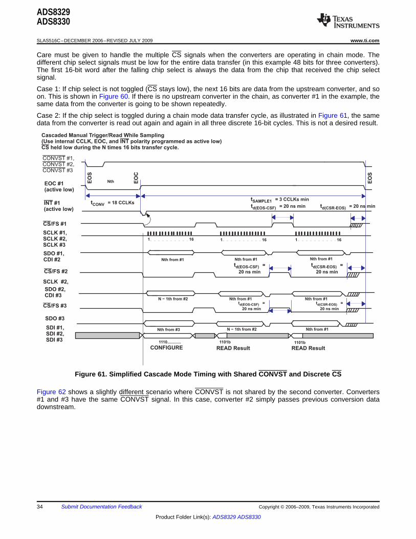
CONFIGURE READ Result READ Result
EO
S
EO
C
EO
S
Nth
Nth from #1 Nth from #1 Nth from #1
Nth from #1 Nth from #1N − 1th from #2
Nth from #3 N − 1th from #2 Nth from #1
1110............ 1101b 1101b
1 16 1 16
Cascaded Manual Trigger/Read While Sampling(Use internal CCLK, EOC, and polarity programmed as active low)
held low during the N times 16 bits transfer cycle.INT
CS
CONVST #1,
CONVST
CONVST
#2,
#3
EOC #1(active low)
INT #1(active low)
CS/FS #3
SCLK #1,SCLK #2,SCLK #3
SDO #1,CDI #2
SDO #2,CDI #3
SDO #3
SDI #1,SDI #2,SDI #3
CS/FS #1
CS/FS #2
SCLK #2,
tCONV = 18 CCLKstSAMPLE1 = 3 CCLKs min
t =
20 ns mind(EOS-CSF)
td(EOS-CSF) =
20 ns min
td(CSR-EOS) = 20 ns min
t =
20 ns mind(CSR-EOS)
td(CSR-EOS) =
20 ns min
td(EOS-CSF) = 20 ns min
1 16
ADS8329ADS8330
SLAS516C–DECEMBER 2006–REVISED JULY 2009 ................................................................................................................................................... www.ti.com
Care must be given to handle the multiple CS signals when the converters are operating in chain mode. Thedifferent chip select signals must be low for the entire data transfer (in this example 48 bits for three converters).The first 16-bit word after the falling chip select is always the data from the chip that received the chip selectsignal.
Case 1: If chip select is not toggled (CS stays low), the next 16 bits are data from the upstream converter, and soon. This is shown in Figure 60. If there is no upstream converter in the chain, as converter #1 in the example, thesame data from the converter is going to be shown repeatedly.
Case 2: If the chip select is toggled during a chain mode data transfer cycle, as illustrated in Figure 61, the samedata from the converter is read out again and again in all three discrete 16-bit cycles. This is not a desired result.
Figure 61. Simplified Cascade Mode Timing with Shared CONVST and Discrete CS
Figure 62 shows a slightly different scenario where CONVST is not shared by the second converter. Converters#1 and #3 have the same CONVST signal. In this case, converter #2 simply passes previous conversion datadownstream.
34 Submit Documentation Feedback Copyright © 2006–2009, Texas Instruments Incorporated
Product Folder Link(s): ADS8329 ADS8330

Note : old data shown.
CONFIGURE READ Result READ Result
EO
S
EO
C
EO
S
Nth
Nth from #1
Nth from #1
Nth from #1
N − 1th from #2
Nth from #3 N − 1th from #2
1110............ 1101b 1101b
1 . . . . . . . . . . . . . . . . . .16 1 . . . . . . . . . . . . . . . . . .16 1 . . . . . . . . . . . . . . . . . .16
Hi-Z
Hi-Z
Hi-Z
Hi-Z
Hi-Z
Hi-Z
Cascaded Manual Trigger/Read While Sampling(Use internal CCLK, EOC active low and active low)
held low during the N times 16 bits transfer cycle.INT
CS
CONVST #1,
CONVST #3
CONVST #2 = 1
EOC #1(active low)
INT #1(active low)
SCLK #1,SCLK #2,SCLK #3
SDO #1,CDI #2
SDO #2,CDI #3
SDO #3
SDI #1,SDI #2,SDI #3
CS/FS #1
CS/FS #2,CS/FS #3
tCONV = 18 CCLKs tSAMPLE1 = 3 CCLKs min
td(CSR-EOS) = 20 ns min
td(CSR-EOS) = 20 ns min
td(SDO-CDI)
td(SDO-CDI)
ADS8329ADS8330
www.ti.com ................................................................................................................................................... SLAS516C–DECEMBER 2006–REVISED JULY 2009
Figure 62. Simplified Cascade Timing (Separate CONVST)
The number of SCLKs required for a serial read cycle depends on the combination of different read modes, TAGbit, chain mode, and the way a channel is selected (that is, auto channel select). This is listed in Table 6.
Table 6. Required SCLKs For Different Read Out Mode CombinationsCHAIN MODE AUTO CHANNEL NUMBER OF SCLK PER SPI
ENABLED CFR.D5 SELECT CFR.D11 TAG ENABLED CFR.D1 READ TRAILING BITS0 0 0 16 None0 0 1 ≥17 MSB is TAG bit plus zero(s)0 1 0 16 None0 1 1 ≥17 TAG bit plus 7 zeros1 0 0 16 None1 0 1 24 TAG bit plus 7 zeros1 1 0 16 None1 1 1 24 TAG bit plus 7 zeros
Copyright © 2006–2009, Texas Instruments Incorporated Submit Documentation Feedback 35
Product Folder Link(s): ADS8329 ADS8330

Logic
Delay
< = 8 .3ns
ADS8329 #3
QD
CLK
Logic
Delay
< = 8 .3 ns
ADS8329 #2
QD
CLK
Logic
Delay
< = 8 .3 ns
ADS8329 # 1
QD
CLK
SCLK input
SDO
SDO
SDO
CDI
CDI
CDI
Serial data
input
Serial data
outputLogicDelay
Plus PAD2.7 ns
LogicDelay
Plus PAD2.7 ns
LogicDelay
Plus PAD8.3 ns
LogicDelay
Plus PAD8.3 ns
LogicDelay
Plus PAD2.7 ns
LogicDelay
Plus PAD8.3 ns
RESET
IntermediateLatch
SAR ShiftRegister
OutputRegister
Conversion Clock
SW RESET
PORSET
Latched by Falling Edge of CSLatched by End OfConversion
EOC
SDO
SCLK
CS
EOC
CDI
ADS8329ADS8330
SLAS516C–DECEMBER 2006–REVISED JULY 2009 ................................................................................................................................................... www.ti.com
SCLK skew between converters and data path delay through the converters configured in chain mode can affectthe maximum frequency of SCLK. The delay can also be affected by supply voltage and loading. It may benecessary to slow down the SCLK when the devices are configured in chain mode.
Figure 63. Typical Delay Through Converters Configured in Chain Mode
The converter has two reset mechanisms, a power-on reset (POR) and a software reset using CFR_D0. Thesetwo mechanisms are NOR-ed internally. When a reset (software or POR) is issued, all register data are set to thedefault values (all 1s) and the SDO output (during the cycle immediately after reset) is set to all 1s. The statemachine is reset to the power-on state.
Figure 64. Digital Output Under Reset Condition
36 Submit Documentation Feedback Copyright © 2006–2009, Texas Instruments Incorporated
Product Folder Link(s): ADS8329 ADS8330

Undefined Zone0.400
0.125
AVDD (V)
t (s)
5.500
5.000
4.000
3.000
2.700
2.000
1.000
0
1.500
Specified Supply
Voltage Range
POR
Trigger Level
0.350
ADS8329ADS8330
www.ti.com ................................................................................................................................................... SLAS516C–DECEMBER 2006–REVISED JULY 2009
When the device is powered up, the POR sets the device to default mode when AVDD reaches 1.5V. When thedevice is powered down, the POR circuit requires AVDD to remain below 125mV for at least 350ms to ensureproper discharging of internal capacitors and to correct the behavior of the ADC when powered up again. IfAVDD drops below 400mV but remains above 125mV, the internal POR capacitor does not discharge fully andthe device requires a software reset to perform correctly after the recovery of AVDD (this condition is shown asthe undefined zone in Figure 65).
Figure 65. Relevant Voltage Levels for POR
Copyright © 2006–2009, Texas Instruments Incorporated Submit Documentation Feedback 37
Product Folder Link(s): ADS8329 ADS8330

APPLICATION INFORMATION
TYPICAL CONNECTION
HostProcessor
FS/CSSDOSDISCLK
CONVST
EOC/INT
4.7 F
+VA REF+ AGND IN+ IN−
4.7 F
Analog +5 V
InterfaceSupply +1.8 V
BDGND
+VBD
Analog Input
ADS8329
REF−
22 F
Ext Ref Input
AGND
AGND
Part Change Notification # 20071101001
ADS8329ADS8330
SLAS516C–DECEMBER 2006–REVISED JULY 2009 ................................................................................................................................................... www.ti.com
Figure 66. Typical Circuit Configuration
The ADS8329 and ADS8330 devices underwent a silicon change under Texas Instruments Part ChangeNotification (PCN) number 20071101001. Details on this part change can be obtained from the ProductInformation Center at Texas Instruments or by contacting your local sales/distribution office. Devices with a datecode of 82xx and higher are covered by this PCN.
38 Submit Documentation Feedback Copyright © 2006–2009, Texas Instruments Incorporated
Product Folder Link(s): ADS8329 ADS8330
ADS8329ADS8330
www.ti.com ................................................................................................................................................... SLAS516C–DECEMBER 2006–REVISED JULY 2009
Revision HistoryNOTE: Page numbers for previous revisions may differ from page numbers in the current version.
Changes from Revision B (March 2008) to Revision C .................................................................................................. Page
• Added 12- and 14-bit rows to family table ............................................................................................................................. 1• Added +REF to AGND and –REF to AGND rows to the Voltage range parameter of the Absolute Maximum Ratings
table ....................................................................................................................................................................................... 2• Changed conditions for 4.5-V Electrical Characteristics........................................................................................................ 3• Changed typ and max specifications for the VREF[(REF+) – (REF–)] parameter in the 4.5-V Electrical Characteristics ...... 4• Changed NAP/Auto-NAP and Deep power-down test conditions of the Supply Current parameter in the 4.5-V
Electrical Characteristics........................................................................................................................................................ 4• Changed conditions for the 2.7-V Electrical Characteristics.................................................................................................. 5• Changed VREF[(REF+) – (REF–)] parameter in the 2.7-V Electrical Characteristics ............................................................. 6• Changed NAP/Auto-NAP and Deep power-down test conditions of the Supply Current parameter in the
Power-Supply Requirements section of the 2.7-V Electrical Characteristics table................................................................ 7• Corrected typo in Figure 1 ................................................................................................................................................... 12• Changed SDO trace of Figure 2 .......................................................................................................................................... 12• Corrected typo in Figure 3 ................................................................................................................................................... 13• Changed SDO trace in Figure 4 .......................................................................................................................................... 13• Corrected typo in Figure 6 ................................................................................................................................................... 14• Added last sentence to Driver Amplifier Choice section...................................................................................................... 23• Updated Figure 52 ............................................................................................................................................................... 24• Updated Figure 53 ............................................................................................................................................................... 24• Changed fifth sentence of Deep Power-Down Mode section .............................................................................................. 27• Changed second sentence of Nap Mode section................................................................................................................ 27• Changed fifth sentence of Auto Nap Mode section ............................................................................................................. 27• Changed power consumption and activation time column values of Table 2...................................................................... 27• Added Figure 65 and corresponding paragraph to RESET section .................................................................................... 37
Changes from Revision A (March 2008) to Revision B .................................................................................................. Page
• Added 16-Pin TSSOP to Features bullet to indicate new package availability ..................................................................... 1• Added 16-Pin TSSOP to third Description paragraph bullet to indicate new package availability ........................................ 1• Changed the Ordering Information table to reflect TSSOP package availability................................................................... 2• Changed Absolute Maximum Ratings table to reflect TSSOP package availability .............................................................. 2• Added pinouts for PW package for both ADS8329 and ADS8330...................................................................................... 10• Added TSSOP column to the ADS8329 Terminal Functions table...................................................................................... 11• Added TSSOP column to the ADS8330 Terminal Functions table...................................................................................... 11• Changed the Part Change Notification section.................................................................................................................... 38
Copyright © 2006–2009, Texas Instruments Incorporated Submit Documentation Feedback 39
Product Folder Link(s): ADS8329 ADS8330

PACKAGE OPTION ADDENDUM
www.ti.com 9-Jul-2017
Addendum-Page 1
PACKAGING INFORMATION
Orderable Device Status(1)
Package Type PackageDrawing
Pins PackageQty
Eco Plan(2)
Lead/Ball Finish(6)
MSL Peak Temp(3)
Op Temp (°C) Device Marking(4/5)
Samples
ADS8329IBPW ACTIVE TSSOP PW 16 90 Green (RoHS& no Sb/Br)
CU NIPDAU Level-2-260C-1 YEAR -40 to 85 ADS8329I AB
ADS8329IBRSAR ACTIVE QFN RSA 16 3000 Green (RoHS& no Sb/Br)
CU NIPDAU Level-2-260C-1 YEAR -40 to 85 ADS8329I A
ADS8329IBRSARG4 ACTIVE QFN RSA 16 3000 Green (RoHS& no Sb/Br)
CU NIPDAU Level-2-260C-1 YEAR -40 to 85 ADS8329I A
ADS8329IBRSAT ACTIVE QFN RSA 16 250 Green (RoHS& no Sb/Br)
CU NIPDAU Level-2-260C-1 YEAR -40 to 85 ADS8329I A
ADS8329IBRSATG4 ACTIVE QFN RSA 16 250 Green (RoHS& no Sb/Br)
CU NIPDAU Level-2-260C-1 YEAR -40 to 85 ADS8329I A
ADS8329IPW ACTIVE TSSOP PW 16 90 Green (RoHS& no Sb/Br)
CU NIPDAU Level-2-260C-1 YEAR -40 to 85 ADS8329I A
ADS8329IPWG4 ACTIVE TSSOP PW 16 90 Green (RoHS& no Sb/Br)
CU NIPDAU Level-2-260C-1 YEAR -40 to 85 ADS8329I A
ADS8329IPWR ACTIVE TSSOP PW 16 2000 Green (RoHS& no Sb/Br)
CU NIPDAU Level-2-260C-1 YEAR -40 to 85 ADS8329I A
ADS8329IRSAR ACTIVE QFN RSA 16 2000 Green (RoHS& no Sb/Br)
CU NIPDAU Level-2-260C-1 YEAR -40 to 85 ADS8329I A
ADS8329IRSAT ACTIVE QFN RSA 16 250 Green (RoHS& no Sb/Br)
CU NIPDAU Level-2-260C-1 YEAR -40 to 85 ADS8329I A
ADS8329IRSATG4 ACTIVE QFN RSA 16 250 Green (RoHS& no Sb/Br)
CU NIPDAU Level-2-260C-1 YEAR -40 to 85 ADS8329I A
ADS8330IBPW ACTIVE TSSOP PW 16 90 Green (RoHS& no Sb/Br)
CU NIPDAU Level-2-260C-1 YEAR -40 to 85 ADS8330I AB
ADS8330IBPWG4 ACTIVE TSSOP PW 16 90 Green (RoHS& no Sb/Br)
CU NIPDAU Level-2-260C-1 YEAR -40 to 85 ADS8330I AB
ADS8330IBPWR ACTIVE TSSOP PW 16 2000 Green (RoHS& no Sb/Br)
CU NIPDAU Level-2-260C-1 YEAR -40 to 85 ADS8330I AB
ADS8330IBRSAR ACTIVE QFN RSA 16 3000 Green (RoHS& no Sb/Br)
CU NIPDAU Level-2-260C-1 YEAR -40 to 85 ADS8330I A

PACKAGE OPTION ADDENDUM
www.ti.com 9-Jul-2017
Addendum-Page 2
Orderable Device Status(1)
Package Type PackageDrawing
Pins PackageQty
Eco Plan(2)
Lead/Ball Finish(6)
MSL Peak Temp(3)
Op Temp (°C) Device Marking(4/5)
Samples
ADS8330IBRSAT ACTIVE QFN RSA 16 250 Green (RoHS& no Sb/Br)
CU NIPDAU Level-2-260C-1 YEAR -40 to 85 ADS8330I A
ADS8330IPW ACTIVE TSSOP PW 16 90 Green (RoHS& no Sb/Br)
CU NIPDAU Level-2-260C-1 YEAR -40 to 85 ADS8330I A
ADS8330IPWG4 ACTIVE TSSOP PW 16 90 Green (RoHS& no Sb/Br)
CU NIPDAU Level-2-260C-1 YEAR -40 to 85 ADS8330I A
ADS8330IPWR ACTIVE TSSOP PW 16 2000 Green (RoHS& no Sb/Br)
CU NIPDAU Level-2-260C-1 YEAR -40 to 85 ADS8330I A
ADS8330IRSAT ACTIVE QFN RSA 16 250 Green (RoHS& no Sb/Br)
CU NIPDAU Level-2-260C-1 YEAR -40 to 85 ADS8330I A
ADS8330IRSATG4 ACTIVE QFN RSA 16 250 Green (RoHS& no Sb/Br)
CU NIPDAU Level-2-260C-1 YEAR -40 to 85 ADS8330I A
(1) The marketing status values are defined as follows:ACTIVE: Product device recommended for new designs.LIFEBUY: TI has announced that the device will be discontinued, and a lifetime-buy period is in effect.NRND: Not recommended for new designs. Device is in production to support existing customers, but TI does not recommend using this part in a new design.PREVIEW: Device has been announced but is not in production. Samples may or may not be available.OBSOLETE: TI has discontinued the production of the device.
(2) RoHS: TI defines "RoHS" to mean semiconductor products that are compliant with the current EU RoHS requirements for all 10 RoHS substances, including the requirement that RoHS substancedo not exceed 0.1% by weight in homogeneous materials. Where designed to be soldered at high temperatures, "RoHS" products are suitable for use in specified lead-free processes. TI mayreference these types of products as "Pb-Free".RoHS Exempt: TI defines "RoHS Exempt" to mean products that contain lead but are compliant with EU RoHS pursuant to a specific EU RoHS exemption.Green: TI defines "Green" to mean the content of Chlorine (Cl) and Bromine (Br) based flame retardants meet JS709B low halogen requirements of <=1000ppm threshold. Antimony trioxide basedflame retardants must also meet the <=1000ppm threshold requirement.
(3) MSL, Peak Temp. - The Moisture Sensitivity Level rating according to the JEDEC industry standard classifications, and peak solder temperature.
(4) There may be additional marking, which relates to the logo, the lot trace code information, or the environmental category on the device.
(5) Multiple Device Markings will be inside parentheses. Only one Device Marking contained in parentheses and separated by a "~" will appear on a device. If a line is indented then it is a continuationof the previous line and the two combined represent the entire Device Marking for that device.
(6) Lead/Ball Finish - Orderable Devices may have multiple material finish options. Finish options are separated by a vertical ruled line. Lead/Ball Finish values may wrap to two lines if the finishvalue exceeds the maximum column width.

PACKAGE OPTION ADDENDUM
www.ti.com 9-Jul-2017
Addendum-Page 3
Important Information and Disclaimer:The information provided on this page represents TI's knowledge and belief as of the date that it is provided. TI bases its knowledge and belief on informationprovided by third parties, and makes no representation or warranty as to the accuracy of such information. Efforts are underway to better integrate information from third parties. TI has taken andcontinues to take reasonable steps to provide representative and accurate information but may not have conducted destructive testing or chemical analysis on incoming materials and chemicals.TI and TI suppliers consider certain information to be proprietary, and thus CAS numbers and other limited information may not be available for release.
In no event shall TI's liability arising out of such information exceed the total purchase price of the TI part(s) at issue in this document sold by TI to Customer on an annual basis.
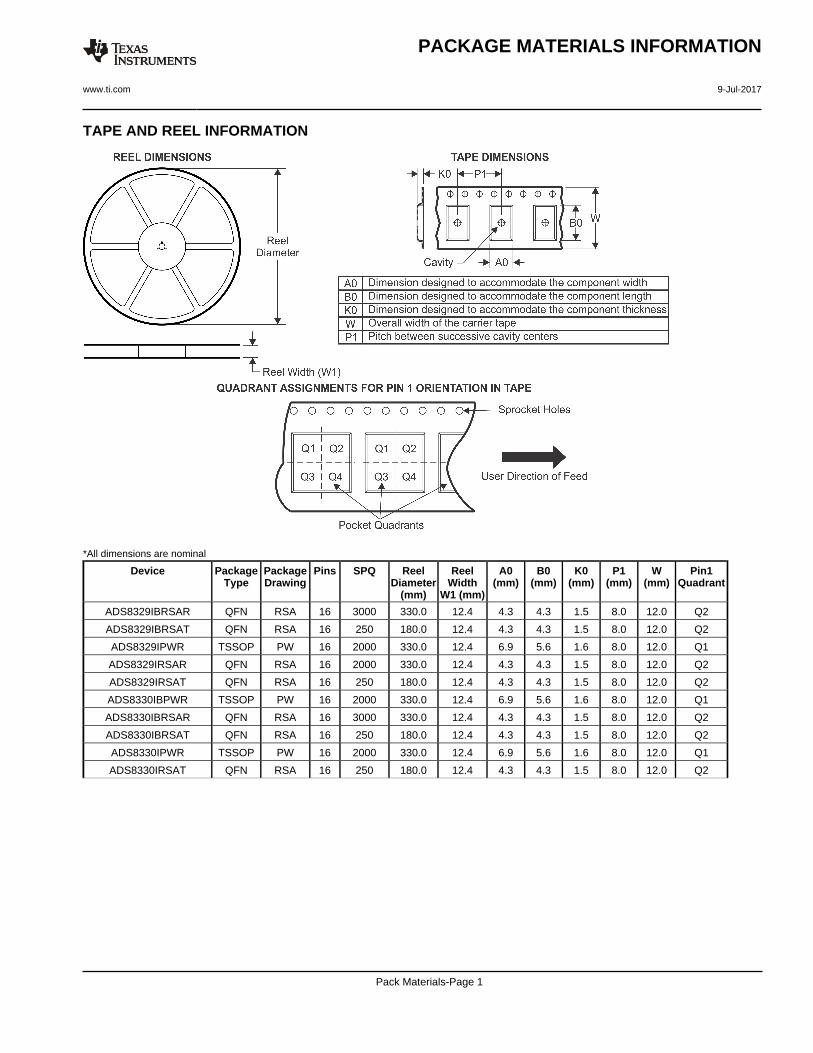
TAPE AND REEL INFORMATION
*All dimensions are nominal
Device PackageType
PackageDrawing
Pins SPQ ReelDiameter
(mm)
ReelWidth
W1 (mm)
A0(mm)
B0(mm)
K0(mm)
P1(mm)
W(mm)
Pin1Quadrant
ADS8329IBRSAR QFN RSA 16 3000 330.0 12.4 4.3 4.3 1.5 8.0 12.0 Q2
ADS8329IBRSAT QFN RSA 16 250 180.0 12.4 4.3 4.3 1.5 8.0 12.0 Q2
ADS8329IPWR TSSOP PW 16 2000 330.0 12.4 6.9 5.6 1.6 8.0 12.0 Q1
ADS8329IRSAR QFN RSA 16 2000 330.0 12.4 4.3 4.3 1.5 8.0 12.0 Q2
ADS8329IRSAT QFN RSA 16 250 180.0 12.4 4.3 4.3 1.5 8.0 12.0 Q2
ADS8330IBPWR TSSOP PW 16 2000 330.0 12.4 6.9 5.6 1.6 8.0 12.0 Q1
ADS8330IBRSAR QFN RSA 16 3000 330.0 12.4 4.3 4.3 1.5 8.0 12.0 Q2
ADS8330IBRSAT QFN RSA 16 250 180.0 12.4 4.3 4.3 1.5 8.0 12.0 Q2
ADS8330IPWR TSSOP PW 16 2000 330.0 12.4 6.9 5.6 1.6 8.0 12.0 Q1
ADS8330IRSAT QFN RSA 16 250 180.0 12.4 4.3 4.3 1.5 8.0 12.0 Q2
PACKAGE MATERIALS INFORMATION
www.ti.com 9-Jul-2017
Pack Materials-Page 1
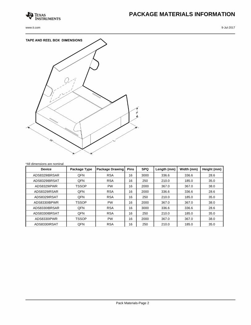
*All dimensions are nominal
Device Package Type Package Drawing Pins SPQ Length (mm) Width (mm) Height (mm)
ADS8329IBRSAR QFN RSA 16 3000 336.6 336.6 28.6
ADS8329IBRSAT QFN RSA 16 250 210.0 185.0 35.0
ADS8329IPWR TSSOP PW 16 2000 367.0 367.0 38.0
ADS8329IRSAR QFN RSA 16 2000 336.6 336.6 28.6
ADS8329IRSAT QFN RSA 16 250 210.0 185.0 35.0
ADS8330IBPWR TSSOP PW 16 2000 367.0 367.0 38.0
ADS8330IBRSAR QFN RSA 16 3000 336.6 336.6 28.6
ADS8330IBRSAT QFN RSA 16 250 210.0 185.0 35.0
ADS8330IPWR TSSOP PW 16 2000 367.0 367.0 38.0
ADS8330IRSAT QFN RSA 16 250 210.0 185.0 35.0
PACKAGE MATERIALS INFORMATION
www.ti.com 9-Jul-2017
Pack Materials-Page 2


IMPORTANT NOTICE
Texas Instruments Incorporated (TI) reserves the right to make corrections, enhancements, improvements and other changes to itssemiconductor products and services per JESD46, latest issue, and to discontinue any product or service per JESD48, latest issue. Buyersshould obtain the latest relevant information before placing orders and should verify that such information is current and complete.TI’s published terms of sale for semiconductor products (http://www.ti.com/sc/docs/stdterms.htm) apply to the sale of packaged integratedcircuit products that TI has qualified and released to market. Additional terms may apply to the use or sale of other types of TI products andservices.Reproduction of significant portions of TI information in TI data sheets is permissible only if reproduction is without alteration and isaccompanied by all associated warranties, conditions, limitations, and notices. TI is not responsible or liable for such reproduceddocumentation. Information of third parties may be subject to additional restrictions. Resale of TI products or services with statementsdifferent from or beyond the parameters stated by TI for that product or service voids all express and any implied warranties for theassociated TI product or service and is an unfair and deceptive business practice. TI is not responsible or liable for any such statements.Buyers and others who are developing systems that incorporate TI products (collectively, “Designers”) understand and agree that Designersremain responsible for using their independent analysis, evaluation and judgment in designing their applications and that Designers havefull and exclusive responsibility to assure the safety of Designers' applications and compliance of their applications (and of all TI productsused in or for Designers’ applications) with all applicable regulations, laws and other applicable requirements. Designer represents that, withrespect to their applications, Designer has all the necessary expertise to create and implement safeguards that (1) anticipate dangerousconsequences of failures, (2) monitor failures and their consequences, and (3) lessen the likelihood of failures that might cause harm andtake appropriate actions. Designer agrees that prior to using or distributing any applications that include TI products, Designer willthoroughly test such applications and the functionality of such TI products as used in such applications.TI’s provision of technical, application or other design advice, quality characterization, reliability data or other services or information,including, but not limited to, reference designs and materials relating to evaluation modules, (collectively, “TI Resources”) are intended toassist designers who are developing applications that incorporate TI products; by downloading, accessing or using TI Resources in anyway, Designer (individually or, if Designer is acting on behalf of a company, Designer’s company) agrees to use any particular TI Resourcesolely for this purpose and subject to the terms of this Notice.TI’s provision of TI Resources does not expand or otherwise alter TI’s applicable published warranties or warranty disclaimers for TIproducts, and no additional obligations or liabilities arise from TI providing such TI Resources. TI reserves the right to make corrections,enhancements, improvements and other changes to its TI Resources. TI has not conducted any testing other than that specificallydescribed in the published documentation for a particular TI Resource.Designer is authorized to use, copy and modify any individual TI Resource only in connection with the development of applications thatinclude the TI product(s) identified in such TI Resource. NO OTHER LICENSE, EXPRESS OR IMPLIED, BY ESTOPPEL OR OTHERWISETO ANY OTHER TI INTELLECTUAL PROPERTY RIGHT, AND NO LICENSE TO ANY TECHNOLOGY OR INTELLECTUAL PROPERTYRIGHT OF TI OR ANY THIRD PARTY IS GRANTED HEREIN, including but not limited to any patent right, copyright, mask work right, orother intellectual property right relating to any combination, machine, or process in which TI products or services are used. Informationregarding or referencing third-party products or services does not constitute a license to use such products or services, or a warranty orendorsement thereof. Use of TI Resources may require a license from a third party under the patents or other intellectual property of thethird party, or a license from TI under the patents or other intellectual property of TI.TI RESOURCES ARE PROVIDED “AS IS” AND WITH ALL FAULTS. TI DISCLAIMS ALL OTHER WARRANTIES ORREPRESENTATIONS, EXPRESS OR IMPLIED, REGARDING RESOURCES OR USE THEREOF, INCLUDING BUT NOT LIMITED TOACCURACY OR COMPLETENESS, TITLE, ANY EPIDEMIC FAILURE WARRANTY AND ANY IMPLIED WARRANTIES OFMERCHANTABILITY, FITNESS FOR A PARTICULAR PURPOSE, AND NON-INFRINGEMENT OF ANY THIRD PARTY INTELLECTUALPROPERTY RIGHTS. TI SHALL NOT BE LIABLE FOR AND SHALL NOT DEFEND OR INDEMNIFY DESIGNER AGAINST ANY CLAIM,INCLUDING BUT NOT LIMITED TO ANY INFRINGEMENT CLAIM THAT RELATES TO OR IS BASED ON ANY COMBINATION OFPRODUCTS EVEN IF DESCRIBED IN TI RESOURCES OR OTHERWISE. IN NO EVENT SHALL TI BE LIABLE FOR ANY ACTUAL,DIRECT, SPECIAL, COLLATERAL, INDIRECT, PUNITIVE, INCIDENTAL, CONSEQUENTIAL OR EXEMPLARY DAMAGES INCONNECTION WITH OR ARISING OUT OF TI RESOURCES OR USE THEREOF, AND REGARDLESS OF WHETHER TI HAS BEENADVISED OF THE POSSIBILITY OF SUCH DAMAGES.Unless TI has explicitly designated an individual product as meeting the requirements of a particular industry standard (e.g., ISO/TS 16949and ISO 26262), TI is not responsible for any failure to meet such industry standard requirements.Where TI specifically promotes products as facilitating functional safety or as compliant with industry functional safety standards, suchproducts are intended to help enable customers to design and create their own applications that meet applicable functional safety standardsand requirements. Using products in an application does not by itself establish any safety features in the application. Designers mustensure compliance with safety-related requirements and standards applicable to their applications. Designer may not use any TI products inlife-critical medical equipment unless authorized officers of the parties have executed a special contract specifically governing such use.Life-critical medical equipment is medical equipment where failure of such equipment would cause serious bodily injury or death (e.g., lifesupport, pacemakers, defibrillators, heart pumps, neurostimulators, and implantables). Such equipment includes, without limitation, allmedical devices identified by the U.S. Food and Drug Administration as Class III devices and equivalent classifications outside the U.S.TI may expressly designate certain products as completing a particular qualification (e.g., Q100, Military Grade, or Enhanced Product).Designers agree that it has the necessary expertise to select the product with the appropriate qualification designation for their applicationsand that proper product selection is at Designers’ own risk. Designers are solely responsible for compliance with all legal and regulatoryrequirements in connection with such selection.Designer will fully indemnify TI and its representatives against any damages, costs, losses, and/or liabilities arising out of Designer’s non-compliance with the terms and provisions of this Notice.
Mailing Address: Texas Instruments, Post Office Box 655303, Dallas, Texas 75265Copyright © 2017, Texas Instruments Incorporated