Low-Noise VHF and L-Band GaAs FET Amplifiers Design Feb 1989 Al Ward.pdf · Reprint'1'j f~.J!11l RF...
5
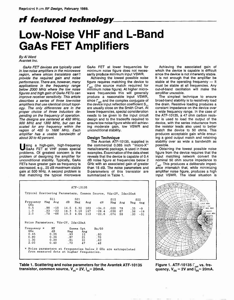
Reprint'1'j f~.J!11l RF Design, February 1989. rl letsfured fechnology _ Low-Noise VHF and L-Band GaAs FET Amplifiers ByAIWard Avantek Inc. GaAs FET devices are typically used in low-noise amplifiers in the microwave region, where silicon transistors can't provide the required gain and noise perlormance. There are, however, many applications in the frequency range below 2000 MHz where the low noise figures and high gain of GaAs FETs can improve receiver sensitivity. This article describes a series of three low-noise amplifiers that use identical circuit topol- ogy. The only differences are in the proper choice of three inductors de- pending on the frequency of operation. The designs are centered at 450 MHz, 900 MHz and 1300 MHz, but can be scaled for any frequency within the region of 400 to 1600 MHz. Each amplifier has a usable bandwidth of about 30 to 40 percent. U sing a high-gain, high-frequency GaAs FET at VHF poses special problems. Of greatest concern is the problem of designing the amplifier for unconditional stability. Typically, GaAs FETs have greater gain as frequency is decreased, e.g., 25 dB maximum stable gain at 500 MHz. A second problem is that matching the typical microwave GaAs FET at lower frequencies for minimum noise figure does not neces- sarily produce minimum input VSWR. Achieving the lowest possible noise figure requires matching the device to ropt (the source match required for minimum noise figure). At higher micro- wave frequencies this will generally produce a reasonable input VSWR, since r opt and the complex conjugate of the device input reflection coefficient S" are usually close on the Smith Chart. At lower frequencies, special consideration needs to be given to the input circuit design and to the tradeoffs required to ensure low noise figure while still achiev- ing moderate gain, low VSWR and unconditional stability. Design Technique The Avantek ATF-10135, supplied in the commercial 0.085 inch "micro-X" metal/ceramic packaqe, is used in these examples. Examination of the data sheet reveals that the device is capable of 0.4 dB noise figure at frequencies below 2 GHz with an associated gain of greater than 15 dB. The noise parameters and S-parameters of this transistor are summarized in Table 1. ATF-10135 Typical Scattering Parameters, Common Source, Vds=2V, Ids=20mA Sl1 521 S12 522 FreqL1ency Mag Ang dB Mag Ang dB Mag Ang Mag Ang GHz 0.5 .98 -18 14.5 5.32 163 -34.0 .020 78 .35 -9 1.0 .93 -33 14.3 5.19 147 -28.4 .038 67 .36 -19 2.0 .79 -66 13.3 4.64 113 -22.6 .074 59 .30 -31 Noise Parameters, Vds=2V, Ids=20mA Frequency * NF Gamma Opt Rn/50 GHz dB Hag Ang 0.45 0.35 .93 12 .80 0.90 0.36 .87 21 .70 1.30 0.38 .81 31 .62 2.00 0.40 .70 47 .46 * Noise parameters at frequencies below 2 GHz are extrapolated from measured data at higher frequencies. Table 1. Scattering and noise parameters for the Avantek ATF-10135 transistor, common source, V DS = 2V, I Ds = 20mA. Achieving the associated gain of which the device is capable is difficult since the device is not inherently stable. It is not enough that the amplifier be stable at the operating frequency - it must be stable at all frequencies. Any out-of-band oscillation will make the amplifier unusable. The simplest technique to ensure broad-band stability is to resistively load the drain. Resistive loading produces a constant impedance on the device over a wide frequency range. In the case of the ATF-10135, a 47 ohm carbon resis- tor is used to load the output of the device, with the series inductance from the resistor leads also used to better match the device to 50 ohms. This produces acceptable gain while ensur- ing a good output match and retaining stability over as wide a bandwidth as possible. Obtaining the lowest possible noise figure from the device requires that the input matching network convert the nominal 50 ohm source impedance to ropt. This produces a deliberate imped- ance mismatch that, while minimizing amplifier noise figure, produces a high input VSWR. The ideal situation is Figure 1. ATF-10135 r OPI vs. fre- quency, Vos= 2V and los= 20mA.
Transcript of Low-Noise VHF and L-Band GaAs FET Amplifiers Design Feb 1989 Al Ward.pdf · Reprint'1'j f~.J!11l RF...
Reprint'1'j f~.J!11l RF Design, February 1989.
rl letsfured fechnology _
Low-Noise VHF and L-BandGaAs FET AmplifiersByAIWardAvantek Inc.
GaAs FET devices are typically usedin low-noise amplifiers in the microwaveregion, where silicon transistors can'tprovide the required gain and noiseperlormance. There are, however, manyapplications in the frequency rangebelow 2000 MHz where the low noisefigures and high gain of GaAs FETs canimprove receiver sensitivity. This articledescribes a series of three low-noiseamplifiers that use identical circuit topol-ogy. The only differences are in theproper choice of three inductors de-pending on the frequency of operation.The designs are centered at 450 MHz,900 MHz and 1300 MHz, but can bescaled for any frequency within theregion of 400 to 1600 MHz. Eachamplifier has a usable bandwidth ofabout 30 to 40 percent.
Using a high-gain, high-frequencyGaAs FET at VHF poses special
problems. Of greatest concern is theproblem of designing the amplifier forunconditional stability. Typically, GaAsFETs have greater gain as frequency isdecreased, e.g., 25 dB maximum stablegain at 500 MHz. A second problem isthat matching the typical microwave
GaAs FET at lower frequencies forminimum noise figure does not neces-sarily produce minimum input VSWR.
Achieving the lowest possible noisefigure requires matching the device toropt (the source match required forminimum noise figure). At higher micro-wave frequencies this will generallyproduce a reasonable input VSWR,since ropt and the complex conjugate ofthe device input reflection coefficient S"are usually close on the Smith Chart. Atlower frequencies, special considerationneeds to be given to the input circuitdesign and to the tradeoffs required toensure low noise figure while still achiev-ing moderate gain, low VSWR andunconditional stability.
Design TechniqueThe Avantek ATF-10135, supplied in
the commercial 0.085 inch "micro-X"metal/ceramic packaqe, is used in theseexamples. Examination of the data sheetreveals that the device is capable of 0.4dB noise figure at frequencies below 2GHz with an associated gain of greaterthan 15 dB. The noise parameters andS-parameters of this transistor aresummarized in Table 1.
ATF-10135Typical Scattering Parameters, Common Source, Vds=2V, Ids=20mA
Sl1 521 S12 522FreqL1ency Mag Ang dB Mag Ang dB Mag Ang Mag AngGHz0.5 .98 -18 14.5 5.32 163 -34.0 .020 78 .35 -91.0 .93 -33 14.3 5.19 147 -28.4 .038 67 .36 -192.0 .79 -66 13.3 4.64 113 -22.6 .074 59 .30 -31
Noise Parameters, Vds=2V, Ids=20mA
Frequency * NF Gamma Opt Rn/50GHz dB Hag Ang0.45 0.35 .93 12 .800.90 0.36 .87 21 .701.30 0.38 .81 31 .622.00 0.40 .70 47 .46
* Noise parameters at frequencies below 2 GHz are extrapolatedfrom measured data at higher frequencies.
Table 1. Scattering and noise parameters for the Avantek ATF-10135transistor, common source, VDS= 2V, IDs= 20mA.
Achieving the associated gain ofwhich the device is capable is difficultsince the device is not inherently stable.It is not enough that the amplifier bestable at the operating frequency - itmust be stable at all frequencies. Anyout-of-band oscillation will make theamplifier unusable.
The simplest technique to ensurebroad-band stability is to resistively loadthe drain. Resistive loading produces aconstant impedance on the device overa wide frequency range. In the case ofthe ATF-10135, a 47 ohm carbon resis-tor is used to load the output of thedevice, with the series inductance fromthe resistor leads also used to bettermatch the device to 50 ohms. Thisproduces acceptable gain while ensur-ing a good output match and retainingstability over as wide a bandwidth aspossible.
Obtaining the lowest possible noisefigure from the device requires that theinput matching network convert thenominal 50 ohm source impedance toropt. This produces a deliberate imped-ance mismatch that, while minimizingamplifier noise figure, produces a highinput VSWR. The ideal situation is
Figure 1. ATF-10135 rOPI vs. fre-quency, Vos= 2V and los= 20mA.

rl feafured fechno/o9Y _
modulation (PPM), reflections due toVSWR manifest themselves as dis-placed pulses, which create direction-finding errors.
To examine the alternatives, constantnoise figure and constant gain circlescan be constructed to assess the impactof trading increased noise figure for adecrease in input VSWR and a corre-sponding increase in amplifier gain. Inmost instances, the result is a muchhigher noise figure than really desired.
An option is to use source feedback.This subject has already been coveredby several authors (References 1-3).Source feedback, in the form of sourceinductance, can improve input VSWRwith minimal noise figure degradation.The drawback of utilizing source induc-tance is a gain reduction of up to severaldecibels. However, GaAs FET devicesoften have more gain than desired at lowfrequencies, so the penalty is not se-vere.
The effect of source inductance onamplifier input match is best studied withthe help of a computer simulation. Thecomputer was used to analyze S11of theamplifier with the proposed output match-ing network. S11was measured lookingdirectly into the gate of the device withthe source inductance added betweenthe source and ground. With the Avan-tek ATF-10135 at 500 MHz, adding the
Lead Length NF Gain :SI1: 2 :822: 2 k k (@ 9 GHz)
0 inch 0.46 dB 20.1 dB -5.4 dB -8.0 dB .75 2.790.1 inch 0.48 dB 17.2 dB -14.3 dB -16.0 dB 1.30 1.940.2 inch 0.52 dB 14.9 dB -10.6 dB -18.4 dB 1.55 0.92
Table 2. Performance VS. source lead length at 900 MHz.
Frequency NF Gain :SI1: 2 : S2 2: 2 k
450 MHz (Measured) : 0.45 dB 21.3 dB -B.O dB -7.6 dB(Simulated) : 0.54 dB 20.6 dB -9.9 -7.0 1.161
900 MHz (Measured) : 0.40 dB 16.5 dB -10.7 dB -14.4 dB(Simulated) : 0.4B dB 1·7.2dB -14.3 dB -16.0 dB 1.30
1300 MHz (Measured) : 0.50 dB 14.5 dB -B.5 dB -17.8 dB(Simulated) : 0.45 dB 15.7 dB -13.0 dB -19.3 dB 1.20
Table 3. Measured performance vs. computer simulation.
wher~ rop' is. the co~plex c~~jugate. ~fS11(i.e., §11). For this condition, mini-mum noise figure is achieved when thedevice is matched for minimum VSWR.This situation occurs predominantlyabove 2 GHz and tends to diverge atlower frequencies, where S11 ap-proaches 1.
High input VSWR has varying signifi-cance, depending on the application.Most noteworthy is the increased uncer-tainty of the noise figure measurement
due to reflections between the noisesource and amplifier input. Similarly,
.when the amplifier is connected to areceive antenna, high input VSWR cre-ates added uncertainty in overall systemperformance. The effect is difficult toanalyze unless an isolator is placed atthe input to the amplifier. The use of anisolator, however, adds excessive lossand, at VHF frequencies, the size of theisolator is often prohibitively large. In thecase of systems using pulse position
QlL=.2"L=.2N Cl
Input ~ SOn. H-::;:-
Output
~ __ -J\fy----1p---",,,,-....., __ C=8~~ Ucc (+)+ ""12VDC
I II = :to mAV II = 1 \' ~ 450 and 900 MHz. 1.4 v i} 1300 MHz
RJ:R4 :R5 :ZI:
68-120n, 1/4-W carbon r-e s Ls t.o r c ved j ue t for v"r220n, 1/4-W carbon res i a t o r-10011, t/4-W carbon resistorIN752. 5.6-V Zf!lIer diodeCompon'·nt.~ rommon t.o all v('r~i(lnt4:
AVllfll"k ATF-iO}:15 l()w-nr)itH~ GHoAs FET100 pF, O.050-inch »que r-e c h i p capacitorIUOO pF, U.050-inch a quu r-e chip capacit.urlOUD pF. O.ttO-inch or O.OSO-inch square chip c apa c i t.c r-0.1 \.IF. a.IIO-inch square chip capacitor1 \.If." e l ec t r n l j- t ic capacitor1000 pF reed t.h r-ouan cflpnci t.o r~ullrr*" ifldllr'-lIn(~f': If'ud J'!II.ct.h on QI IIf'r I.nhll!IR-331l. 1/4-W ce r-bcn r es t s t.o r-o-ed jue t, for I!, ~ 20 cnA
4ifl. 1/·l-W ce ebon r-e s i s t.or- with 0.15" f euda , lap 0.1" from 'H 1
c i :CI. C~:ca. (;4:CS:C6 :C7 :CK:L2. 1.3;Rl:R2 :
Componen t.s c h an ze d with r r-e qu enc y 0 f opera t. i on;
Pr-equenc y 150 MHz DOO MHzsuo Mllz
molded RFCj)RFC 1:Ll:
0.47 ""HT ,28.I/R" J. n.
clo.Mt.!-wound0.125"
0.:1 3 uBJT ,2H,I/A" J. O.
: -'Spact!d I0.10"
0.33 uH Imin.3T .ZH,0.050" I. O.
wirt' diUlllet.er-Q:.06S"1.2. L:t
50n e Lc r-o e t r t p l Lne s are .080" wide on RT/DuTOld 5880, .o:n '-thick
Figure 2. Schematic of the GaAs FET amplifier circuit. The only change made to modify the operating·frequency range from 400 to 1500 MHz is changing the values of RFC1 and L1.
rl feafured fechnology _
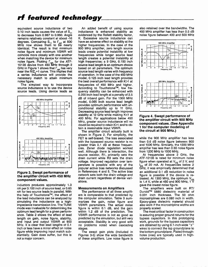
equivalent source inductance of two0.10 inch leads causes the value of S"to decrease from 0.987 to 0.960. Angleremains relatively constant at about -16degrees. Comparing S" to roptat 500MHz now shows them to be nearlyidentical. The result is that minimumnoise figure and minimum VSWR willcoincide more closely with one anotherwhen matching the device for minimumnoise figure. Plotting roptfor the ATF-10135 device from 450 MHz through 2GHz in Figure 1 shows that roptlies verynear the RlZo=1 curve. This implies thata series inductance will provide thenecessary match to attain minimumnoise figure.
The simplest way to incorporatesource inductance is to use the devicesource leads. Using device leads as
450 MHz Amplifier
./ I'\. ~r-,i\ s•• r-
V
II
II-.S -10
f
".
.1 .3 .5 .7 ,9 1.1 1.3 1.5 1.7 1.9 2.1Frequ.ncy, GHz
450 MHz Amplifier
r ~,,.~' rl ~ 1 III I~' , 'Ir 'l'lrl Ili"1
II
II -5
i -10
}-"
II<3
-10 ~
-20 J•-30 iit.....•
.1 .3 .5 .7 .9 1.1 1.3 1.5 1.7 1.9 2.1Frequency, GHz
Figure 3. Swept performance ofthe amplifier circuit with 450 MHzcomponent values.inductors produces approximately 1.3nH per 0.100 inch of source lead, or 0.65nH for two source leads in parallel. Withthe help of TouchstoneTM, the effect ofthe lead inductance can be analyzed bysimulating the inductance as a high-impedance transmission line. The TUNEmode was invaluable for determining theoptimum lead length for a given perform-ance. Table 2 shows the effect of leadlength on gain, noise figure, stability,and input and output VSWR at 900MHz. It is clear that lead lengths Of 0.1inch or less have a minor effect on noisefigure while improving input match sub-stantially. Gain does suffer, but this isnot a major concern.
An added benefit of using sourceinductance is enhanced stability asevidenced by the Rollett stability factor,K. Excessive source inductance canhave an adverse effect on stability at thehigher frequencies. In the case of the900 MHz amplifier, zero length sourceleads create potential instability at lowfrequencies while longer source leadlength creates a potential instability athigh frequencies; a 9 GHz, 0.100 inchsource lead length is an optimum choicebased on all parameters. The optimumsource lead length varies with frequencyof operation. In the case of the 450 MHzmodel, 0.125 inch lead length providesthe best overall performance with K>1 atfrequencies of 450 MHz and higher.According to Touchstone TM, low fre-quency stability can be enhanced with0.200 inch lead length at a penalty of 2.5dB of inband gain. For the 1300 MHzmodel, 0.065 inch source lead lengthprovides optimum performance with un-conditional stability up to 11 GHz.Decreasing source lead length improvesstability at 12 GHz while making K<1 at400 MHz. For applications below 450MHz, greater source inductance will nodoubt be required to retain K>1 and to ob-tain a reasonable input VSWR.
The amplifier circuit actually built isshown in Figure 2. For simplicity, theFET is self-biased. The loss associatedwith the bypassed source resistor is nogreater than 0.1 dB at these frequen-cies. Zener diode regulation workedwell. Although there is interaction, thesource resistor, R1, primarily sets thedrain current while R3 sets the drainvoltage. Improved regulation over tem-perature is possible with any of thepopular active bias networks discussedin References 4 and 5. The active biasnetwork sets both the drain voltage anddrain current regardless of device vari-ations.
Measurements on AmplifiersThe performance of all three amplifi-
ers is comparable to that predicted bythe computer simulation. Table 3 sum-marizes the gain, noise figure andVSWR parameters. The actual noisefigure is within 0.1 dB, and the gainwithin 1.2 dB of the prediction. TheVSWR performance is not as good aspredicted by the simulation, but still veryacceptable. Stability is very good withno problems noted when cascadingstages.
The swept gain plots (included inFigures 3-5) show the wide bandwidthof these amplifiers. Low noise figure is
also retained over the bandwidths. The450 MHz amplifier has less than 0.5 dBnoise figure between 400 and 500 MHz
900 MHz Amplifier
~~ -r--i--
<, .r\ I ~
,2.
.1 .3 .5 .7 ., t.I 1.3 1.5 1.7 1.9 2.1F~quency. GH:
900 MHz Amplifier
~,,.(
Ml! J'TI I ?2
II
II -.I-tO}-"
I• ;!_'·1-20 ~
-30 ~if....•
.1 .3 .5 .7 .9 1.1 1.3 1.5 1.7 1.9 2.1Fl1!'qu~ncy.GH:
Figure 4. Swept performance ofthe amplifier circuit with 900 MHzcomponent values. (See Appendix1 for the computer modeling ofthe circuit at 900 MHz.)
while the 900 MHz amplifier has lessthan 0.6 dB noise figure between 800and 1000 MHz. Similarly, the 1300 MHzamplifier has less than 0.65 noise figurefrom 1200 MHz to 1500 MHz.
At frequencies above 2 GHz. theATF-10135 is rated for minimum noisefigure when operated at VD~ of 2 V, andI of 20 mA. At frequencies below 2~fiz, it was empirically determined thatan additional 0.1 dB reduction 'in noisefigure is possible if the device is re-biased. At 1300 MHz, the optimum Vosis 1.4 V, while at 450 and 900 MHz, 1 Vgave the lowest noise figure.
The amplifiers were built on RTIDuroid" 5880 dielectric material of0.031 inch thickness. The 50 ohmmicrostriplines are 0.080 inch in width.Epoxy-glass dielectric material shouldalso work if the microstripline widths areproperly scaled.
The most critical factor in constructionis assuring proper ground returns for thebypass capacitors. In this prototypingwork, grounds for the bypass capacitorsare obtained by using 0.1-inch-wide "z"wires to connect the top groundplane tothe bottom groundplane. Plated through-holes (vias) are typically used in high-volume production.

rllealured lechno/ogy _
For enclosures, standard Hammondor Bud diecast aluminum boxes areappropriate; the microstripline board fitsnicely into the lid of a Hammond 1590Adiecast aluminum box. Flange mountSMA- type connectors are suggested toensure mechanical rigidity. The connec-tor mounting hardware is used to pro-vide a good mechanical and RF connec-tion between the connector, the box andthe groundplane side of the microstriplineboard.
Amplifier TuningThe inherent broad bandwidth of
these amplifiers drastically reduces thetime required to get them into operation.Setting up each amplifier is simple.
1300 MHz Amplifier--
1s"
~ r-- <, -I-<,____ I-""
,Ij -.
-10
j.1 .3 .5 .7 .9 1.1 1.3 1.5 1.7 1.9 2.1
Frequency, GHz
_____ ~O!!l_l-!z Amplifier
--- -- --- I--- -
~.•L, Wif, r""" ./ S;;-
1)'1 n' """'" / •..•0.1 .3 .5 .7 .9 1.1 1.3 1.5 1.1 1.9 2.1
Frequency, GHz
Figure 5. Swept performance ofthe amplifier circuit with 1300 MHzcomponent values.
Once the device is set up for the properDC operating parameters for the fre-quency of interest, noise figure and gainperformance should be comoarable tothat shown in Table 3. If necessary,adjust the turns spacing on the inputinductor for the desired input VSWR.This will automatically coincide withminimum noise figure and maximumgain. As shown in the foregoing data, thenoise figure varies very little over a widebandwidth, so it might be advantageousto tune for minimum input VSWR asopposed to noise figure. Without the
source inductance, the input VSWR willbe considerably higher.
The simple series UR matching net-work in the output circuit forces a goodbroadband low VSWR output match.Due to the finite amount of reverseisolation of the device, the output matchis affected by the input match and viceversa. Therefore the frequency of bestoutput VSWR is somewhat dependenton where the input network is optimum.
Using the Design at OtherFrequencies
The basic amplifier design can beadapted for any frequency in the 400 to1600 MHz range. Merely scaling theinput inductor for the desired frequencywill allow operation on a different fre-quency. The graph shown in Figure 6gives some idea of the relationship of L
Inductance (L 1) vs. Frequency150
\1\<, '---r-
:r': 100gtl~ 50
a 0.1 0.5 1.0 1,5 2,0Frequency, GHz
Figure 6. Inductance of L1 vs.frequency in the amplifier circuit .vs. frequency - source feedback shouldbe adjusted accordingly. The ATF-10135 has been used successfully incircuits operating at as low as 150 MHzwith similar results.
ConclusionThe results show that high-frequency
GaAs FETs can be used very success-fully in the 400 to 1600 MHz frequencyrange. This same technique can be useddown to 150 MHz and up to 1.7 GHz withsimilar results.Conventionalmicrostriplinematching techniques will still offer thebest performance above 1.76 GHz.
The single-element match in the inputnetwork provides very good perform-ance in this frequency range and offersthe greatest bandwidth. There is no
doubt that noise figure and input VSWRperformance can be further enhancedby the use of a two-element matchingnetwork. A shunt capacitor can be usedon the device side of the input inductor,but this may necessitate additional tun-ing for very little improvement in per-formance. Present noise figure perform-ance is already within 0.1 dB of thatspecified in the data sheet.
Improved VSWR performance at theexpense of increased noise figure canbe achieved by a further increase insource inductance. Overall amplifierperformance is best analyzed with thehelp of the computer.
When using any GaAs FET in the VHFregion, it becomes even more difficultto obtain broadband stability due to thehigh gain available from the device. Forthis reason, a broadband resistive loadwas chosen for the output network asopposed to the typical UC tank circuit.Some gain is sacrificed for the addedbenefit of increased stability.
[Appendix 1 follows on p. 48]
References1. L. Besser, "Stability Considerationsof Low Noise Transistor Amplifiers WithSimultaneous Noise and Power Match, II
Low Noise Microwave Transistors andAmplifiers, H. Fukui, Editor, IEEE Press,1981, pp. 272-274.2. G.D. Vendelin, "Feedback Effects onthe Noise Performance of GaAsMESFETs, II Low Noise Microwave Tran-sistors and Amplifiers, H. Fukui, Editor,IEEE Press, 1981, pp. 294-296.3. D. Williams, W. Lum, S. Weinreb,"L-Band Cryogenically Cooled GaAsFET Amplifiers, II Microwave Journal,October 1980, p. 73.4. G. Gonzalez, Microwave TransistorAmplifiers, Prentice-Hall, 1984, pp. 131-133.5. G.D. Vendelin, Design of Amplifiersand Oscillators by the S-ParameterMethod, Wiley, 1982, pp. 53-59.
About the AuthorAI Ward is a field applications
engineer at Avantek, MicrowaveSemiconductor Division, 101 WestRenner Road, Suite 180,Hichardson, TX 75081. He can bereached at (214) 437-5694.
Touchatone (1M) - ConfilJuration( 100 1500 100 16437. 2384 1000 I 3294 )900AMP.CKT Thu Dee 29 16: 19: 3B 1988
DIM
VAR
CKT
FREQ GHZIND NH'CAP PFLNG IN
LL=O.1CC=1000
MSUB ER=2.1 H=.031 T=.001HLIN 1 2 W=.080 1.=.2SLC 2 3 1.=.5 C=100HLIN 3 4 W=.080 1.=.2IND 4 5 1.\40IND 4 8 1.=330RES 8. 0 R=100DU2P 1..' 5 NAIN
A:\S_DATA\10135N.S2P.NA2P
HLIN 9 :10'" W=.;020 .L-LL~~N ~1 d~~::~20 C_~~LLRIBBON12 .0 .: W•. l L=.031
~tiBOll~3'1~ \,~~: ~ ~:~g31RES 10 O' R.41DEFIP 9 NASIR
HLIN 8 14 W'.080 1.•. 1IND 14, 15, L.I0RES 15 16 R'41SLC 18 0 1.e ,'5' C.I000
RHO.1 RGH.O
RHO.1
RHO.l
Touchaton •• (TM) - ConfilUration( 100 1500 100 16431 2364 1000 1 3294900AMP.OUT Thu Dee 29 15:41:35 1988 LL. 0.0 Inch.
FREQ-GHZDB[Sl1J DB[S2'i] DB[S21J DB[612J DB[NYJ KAMP AMP AMP AMP AMP AMP
0.100000.300000.500000.700000.900001.100001,300001. 50000
,1.700001.900002,100002.300002.500002.100002.900003.100003.300003.500003.700003.900004.100004.300004.500004.700004.900005.100005.300005.500005.700005.900008.100006.300008.50000S.700006.900007.100007.300007.50000
. 7.700001.900008.100008.300008.500008.700008.90000S.100009.300009.500009.700009. SOOOO10.100010.300010.500010.700010.900011.100011. 300011. 500011.700011. SOOO12.0000
-1. 524-0.112-0.368-2.261-5.390-1.182-0.501-0.281-0.189-0.135-0.105-0.087-0.074-0.068-0.059-0.055-0.051-0.04S-0.048-0.047-0.047-0.047-0.048-0.048-0.049-0.050-0.050-0.051-0.051-0.051-0.051-0.050-0.049-0.048-0.041-0.045-0.043-0.041-0.039-0.031-0.035-0.033-0.032-0.030-0.028-0.027-0.028-0.025-0.024-0.023-0.022-0.022-0.022-0.021-0.021-0.022-0.022-0.022-0.023-0.025-0.025
-11.731 9.824 -49.925-H.S19 11.808 -40.835-15.880 14.535 -33.837-14.581 lS.383 -28.114-8.048 20.141 -23.061-8.803 13.754 -27.448-8.961 9.020 -30.305-8.887 5.603 -32.024-8.885 2.928 ,-33.141-8,391 0.721' '-33.919-8.131 -1.093 -34.450-7.897 -2.817 -34.832-7.707 -3.958 -35.118-7.565 -5.147 -35.323-7.417 -6.203 -35.487-7.438 -7.127 -35.608-1.450 -1.939 -35.149
• -7.525 ." -8.888 -35.848-7.88S -S.324 ,·-35.905,-7.888 .. -9.S18 -35.S35-8.185 -10.488 -35.914-8.588 -11.030, -38.023-9.054 -11.521 -38.051-9.885 -11.989 -38.088
-10.427 -12.384 -38.082-11.039 -12.195 -38.099-11. 411 -13.204 -38.109-11.888 -13.595 -38.112-12.522 -13.913 -36.120-13.358 -14.344 -38.141-14.085 -14.735 -36.281-13.942 ~15.155 -36.505-13.485 -15.585 -36.894-13.038 -18.022 -38.848-12.889 -16.465 -38.968-12.468 -16.950 -31.152-11.521 -11.411 -31.408-10.611 -17.981 -37.633-9.911 -18.413 -31.828-9.264 -18.941 -31.983-8.674 -19.361 -38.158-1.617 -19.601 -38.375-7.111 -20.198 -38.511-6.473 -20.564 -38.740-5.884 -20.698 -38.815-5.480 -21.208 -39.036-5.251 -21. 505 -39,223-5.059 -21.182 -39.366
.. -4.904 -21.913 -39.451.. -4.161 -22.131 -39.490..--4.161 -22.305 -39,521. -4.869 -22 •• 99 -39,546
-5.051 -22.833 -39,498-5.276 -22.702 -39.363-5.592 -22.896 -39.141-5.895 -22.838 -38.938-8.179 -22.526 -38,165-8.588 -22.346 -36.514-1.112 -22.090 -36.175-6.016 -21.155 -37.146-8.585 -21.556 -37,498
3.0932.2431.1890.9060.4580.9942.5004.4136.3021.9999.893
11. 98313.88415.56717.11918.54019.84121.02522.06222.99523.70024.27124.78925.18225.49325.68025.72125.59725.28624.71025.01425.97826.89827.21927.58227.82627.98028,05828.07828.04328.24728.89029.09229.45929.19230.09230.35930.59730,60630.98831.14631. 28131. 36931.47131. 52731. 55931. 56631. 54531.49531. 41631. 365
14.2190.6810.5710.6810.7550.8340.9010.9410.9650.9800.9981.0211.0441.0691.0951.1231.1541.1901.2311.2781. 3341.4001.4131.6541. 6421. 7331.8221.9111. 9992.0882.1892.3032.4052.4972.5182.6682.7572.8312.8862.9182.9352.9392.9232.8812.8292.7922.1802.1802.1292.8902.8822.7012.7242.1312.7252.1152.7042.6652.6562.8152.590
5LC 16 0 1.=.5 C.I0000MLIN 1417 W,,080 L=.1SLC 17 18 L=.5 C=100MLIN 18 19 W=.060 L=.2
DEF2P8 19 NAOOT
NAIN 1 5NA2P 5 8 9NAsllR9NAOUT6 19DEF2P1 19 AMP
FREQ
OUT
OPT
ISTEP ,900SWEEP0.100 12.0ISTEP 9,0
AMP DB[611]AMP DB[S22]AMP DB(S21]AMP DB[S12JAMP DB[NY]AMP K
AMP DB[NYJ<.2!AMP DB[S21J>25
.2
Touchstone (TH) - Conficurotion( 100 1500 100 16437 2364 1000 1 3294900AMP.OUT Thu Dee 29 15:40:06 1988 L:'. 0.1 !neh
FREQ-GHZDB(Gl1J DB[S22] DB[521J DB[512J DB(NYJ KAMP AMP AMP AMP AMP AMP
0.100000.300000.500000.700000.900001.100001.300001. 500001.700001,900002.100002.300002.500002.700002.900003.100003.300003.500003.700003.900004.100004.300004.500004.700004. SOOOO5.100005.300005.500005.700005.900008.100006,300008.500006.100008.900007.100001.300001.500001.100001.900008.100008.300008.500008.700008.900009.100009.300009,500009.700009.9000010.100010.300010. BOOU10.100010.900011.100011.300011.500011.100011.900012.0000
-1. 545-0.321-0.919-4.230
-14.264-2.997-1. 244-0.681-0.431-0.297-0.222-0.178-0.145-0.122-0.106-0.094-0.085-0.078-0.073-0.069-0.068-0.064-0.062-0.062-0.061-0.061-0.060-0.060-0.059-0.058-0.057-0.055-0.054-0.052-0.050-0.047-0.045-0.042-0.040-0.031-0.035-0.032-0.030-0.028-0.028-0.024-0.022-0.021-0.019-0.018-0.017-0.018-0.015-0.015-0.015-0.015-0.015-0.018-0.017-0.016-0.019
-11.796-14,549-14.361-14.979-15.983-12.778-11. 060-9.960-9.130-8.462-7.933-7.521-7.192-8.939-6.755-8.631-8.562-6.558-8.612-6,734-6.926
'-7.186-7.530-7.965-8.508-8.948-9.213-9.540-9.972
-10.549-11.226-11.550-11,539-11.391-11.323-11,157-10.661-10.119-9.583-9.033-8.418-7.880-1.323-8.613-8.358-6,091-8.019-5.991-8.021-6.117-8.402-8.851-7.329-1.731-7.938-7.882-7.509-8.824-5.926-4. 989-4.507
9.61911.40713.75116.81811.'20613.0408.8885.6282.9930.798
-1. 029-2.589-3.924-5,122-8,183-1.108-7.917-8.841-9.290-9.814
-10.434-10.968-11.443-11.877-12.277-12.878-13.080-13.464-13.835-14.198-14.579-14,992-15.418-15.858-16.303-18.793-17.320-17.842-18.349-18.837-19.298-19.139-20.155-20.541-20.886-21.211-21. 526-21. 804-22.040-22.232-22.470-22.784-23.094-23.415-23.766-24.143-24.566-25.080-25.702-26.440-26,851
-50.033-40.783-33.875-27.388-24.221-25.644-27.571-28.677-29.383-29.848-30.187-30.458-30.864-30.819-30.935-31.039-31.135-31,203-31,250-31. 260-31.326-31. 391-31. 450-31. 511-31. 583-31.859-31. 713-31. 754-31.795-31. 847-32.041-32,335-32.572-32.733-32.809-32.973-33.277-33.584-33.828-34.085-34.330-34.852-34.984-35.320-35.856-35.949-38.175-36,358-38.494-36.577-36.581-36.502-36.319-38.235-36.101-35.997-35.917-35.897-35.970-38,157-36.297
3.0902.2401.7100.9120.4821.0442.5634.4706.3408.0139.883
11,94813.80315,48017.00818.40419.68520.84921. 89022.79023.48224.04124.53124.94125.25425.44325.48225,35625.05324,54824.81525.80228.53827.07027.43727.69427.87327.97628.02028.01428.25328.14129.19829.82630.03030,40530.14831.08931.37031. 85031.93032,21032.47332.72132.95533.18933.42333.64333.84734.03534.122
14.5961.1481.1511. 2621.2971. 3051.2811. 2521. 2151,1781.1561.1481.1421.1401.1411. 1421.1441.1481.1561.1671.1651.2111. 2411. 2751. 3131. 3561.3991. 4411. 4801.5171.5851.6271.6811.7251. 7541. 7901. 8401. 8821. 9161. 9401.9541. 9841.9661.9611. 9481,9341. 9191.8971.8891.6341. 8071. 7911. 7751.7611. 7531. 7381. 7191.7141.7271,1621.790
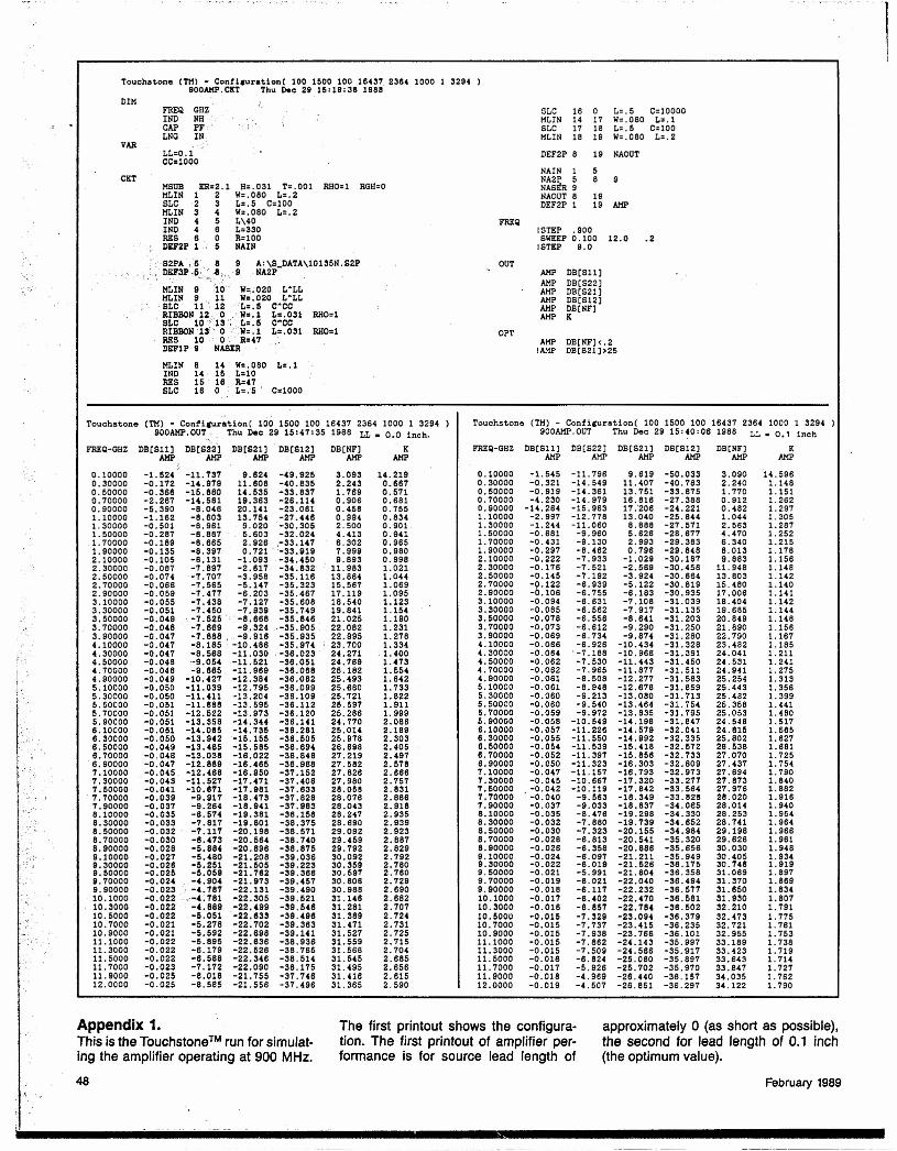
Appendix 1.This is the Touchstone" run for simulat-ing the amplifier operating at 900 MHz.
48
The first printout shows the configura-tion. The first printout of amplifier per-formance is for source lead length of
approximately 0 (as short as possible).the second for lead length of 0.1 inch(the optimum value).
February 1989


![LOW-NOISE, 1.25 GHz, COOLED, HENT AMPLIFIERlibrary.nrao.edu/public/memos/edtn/EDTN_151.pdf · [5] Manuel Sierra, "15 GHz Cooled GaAs FET Amplifier--Design Background Information,"](https://static.fdocuments.in/doc/165x107/60ee979aa360d31402316a32/low-noise-125-ghz-cooled-hent-5-manuel-sierra-15-ghz-cooled-gaas-fet.jpg)