
SECTION 104dot.alaska.gov/creg/design/highways/specs/Proj_Specs_Archive/CFH… · Web viewSECTION 104

Low-noise, High-dynamic-range AM/FM Antenna Amplifier IC
ATR4251
4913J–AUDR–10/09
Features• High Dynamic Range for AM and FM• Integrated AGC for AM and FM• High Intercept Point 3rd Order for FM• FM Amplifier Adjustable to Various Cable Impedances• High Intercept Point 2nd and 3rd Order for AM• Low Noise Output Voltage• Low Power Consumption• Low Output Impedance AM
1. DescriptionThe ATR4251 is an integrated low-noise AM/FM antenna amplifier with integratedAGC in BiCMOS2S technology. The device is designed in particular for car applica-tions, and is suitable for windshield and roof antennas.
Figure 1-1. Block Diagram QFN24 Package
CREGNC*
NC*
Paddle = GND
AGCCONST
AMOUT1
GND1
VREF4
VS
NC*
AGC1
VREF2
AMIN
AGC2
GND
NC*TCONST
AGCAM
AGC(AM)
AGCAMIN
VREF1FMIN
AGCIN
FMGAIN
FMOUTGND2
FMamplifier
8 10 12119
5
3
4
1
2
6
14
16
15
18
17
13
7
23 21 19202224
BANDGAP
AM
AGC
* Pin must not be connected to any other pin or supply chain except GND.

Figure 1-2. Block Diagram SSO20 Package
FMIN
VREF1
GND
AGC1
AGC2
AGCAMIN
CREG
AMIN1
VREF2
FMGAIN
2
3
4
5
6
10
9
8
7
1
FMOUT
AGCIN
VS
AGCCONST
VREF4
AGCAM
TCONST
GND1
AMOUT1
GND2
19
18
17
16
AGC(AM)
Bandgap
AGC
SSO20
FMamplifier
15
11
12
13
14
20
AM
24913J–AUDR–10/09
ATR4251
ATR4251
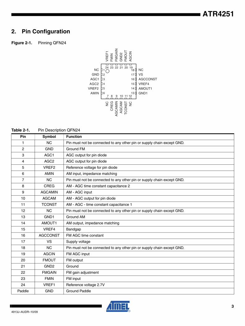
2. Pin Configuration
Figure 2-1. Pinning QFN24
NCGND
AGC1
AGC2VREF2
AMIN
NCVSAGCCONST
VREF4AMOUT1GND1
VR
EF
1F
MIN
FM
GA
ING
ND
2F
MO
UT
AG
CIN
NC
CR
EG
AG
CA
MIN
AG
CA
M
TC
ON
ST
NC
24 23 22 21 20 19
7 8 9 10 11 12
18
17
16
15
14
13
1
2
3
4
5
6
Table 2-1. Pin Description QFN24
Pin Symbol Function
1 NC Pin must not be connected to any other pin or supply chain except GND.
2 GND Ground FM
3 AGC1 AGC output for pin diode
4 AGC2 AGC output for pin diode
5 VREF2 Reference voltage for pin diode
6 AMIN AM input, impedance matching
7 NC Pin must not be connected to any other pin or supply chain except GND.
8 CREG AM - AGC time constant capacitance 2
9 AGCAMIN AM - AGC input
10 AGCAM AM - AGC output for pin diode
11 TCONST AM - AGC - time constant capacitance 1
12 NC Pin must not be connected to any other pin or supply chain except GND.
13 GND1 Ground AM
14 AMOUT1 AM output, impedance matching
15 VREF4 Bandgap
16 AGCCONST FM AGC time constant
17 VS Supply voltage
18 NC Pin must not be connected to any other pin or supply chain except GND.
19 AGCIN FM AGC input
20 FMOUT FM output
21 GND2 Ground
22 FMGAIN FM gain adjustment
23 FMIN FM input
24 VREF1 Reference voltage 2.7V
Paddle GND Ground Paddle
34913J–AUDR–10/09

Figure 2-2. Pinning SSO20
FMGAINFMIN
VREF1GND
AGC1AGC2
VREF2AMIN1CREG
AGCAMIN
GND2FMOUTAGCINVSAGCCONSTVREF4AMOUT1GND1TCONSTAGCAM
12345678910
20191817161514131211
Table 2-2. Pin Description SSO20
Pin Symbol Function
1 FMGAIN FM gain adjustment
2 FMIN FM input
3 VREF1 Reference voltage 2.7V
4 GND FM ground
5 AGC1 AGC output for PIN diode
6 AGC2 AGC output for PIN diode
7 VREF2 Reference voltage for PIN diode
8 AMIN1 AM input, impedance matching
9 CREG AM AGC constant capacitance 2
10 AGCAMIN AM input, AM AGC
11 AGCAM AM AGC output for PIN diode
12 TCONST AM AGC constant capacitance 1
13 GND1 AM ground
14 AMOUT1 AM output, impedance matching
15 VREF4 Band gap 6V
16 AGCCONST FM AGC constant
17 VS Supply voltage
18 AGCIN FM AGC input
19 FMOUT FM output
20 GND2 FM ground
44913J–AUDR–10/09
ATR4251

ATR4251
3. Functional DescriptionThe ATR4251 is an integrated AM/FM antenna impedance matching circuit. It compensatescable losses between the antenna (for example windshield, roof, or bumper antennas) and thecar radio which is usually placed far away from the antenna.
AM refers to the long wave (LW), medium wave (MW) and short wave (SW) frequency bands(150 kHz to 30 MHz) that are usually used for AM transmission, and FM means any of the fre-quency bands used world-wide for FM radio broadcast (70 MHz to 110 MHz).
Two separate amplifiers are used for AM and FM due to the different operating frequencies andrequirements in the AM and FM band. This allows the use of separate antennas (for example,windshield antennas) for AM and FM. Of course, both amplifiers can also be connected to oneantenna (for example, the roof antenna).
Both amplifiers have automatic gain control (AGC) circuits in order to avoid overdriving theamplifiers under large-signal conditions. The two separate AGC circuits prevent strong AM sig-nals from blocking FM stations, and vice versa.
3.1 AM AmplifierDue to the long wavelength in AM bands, the antennas used for AM reception in automotiveapplications must be short compared to the wavelength. Therefore these antennas do not pro-vide 50Ω output impedance, but have an output impedance of some pF. If these (passive)antennas are connected to the car radio by a long cable, the capacitive load of this cable (some100 pF) dramatically reduces the signal level at the tuner input.
In order to overcome this problem, ATR4251 provides an AM buffer amplifier with low inputcapacitance (less than 2.5 pF) and low output impedance (5Ω). The low input capacitance of theamplifier reduces the capacitive load at the antenna, and the low impedance output driver is ableto drive the capacitive load of the cable. The voltage gain of the amplifier is close to 1 (0 dB), butthe insertion gain that is achieved when the buffer amplifier is inserted between antenna outputand cable may be much higher (35 dB). The actual value depends, of course, on antenna andcable impedance.
The input of the amplifier is connected by an external 4.7 MΩ resistor to the bias voltage (pin 7,SSO20) in order to achieve high input impedance and low noise voltage.
AM tuners in car radios usually use PIN diode attenuators at their input. These PIN diode atten-uators attenuate the signal by reducing the input impedance of the tuner. Therefore, a seriesresistor is used at the AM amplifier output in the standard application. This series resistor guar-antees a well-defined source impedance for the radio tuner and protects the output of the AMamplifier from short circuit by the PIN diode attenuator in the car radio.
54913J–AUDR–10/09

3.2 AM AGCThe IC is equipped with an AM AGC capability to prevent overdriving of the amplifier in case theamplifier operates near strong antenna signal level, for example, transmitters.
The AM amplifier output AMOUT1 is applied to a resistive voltage divider. This divided signal isapplied to the AGC level detector input pin AGCAMIN. The rectified signal is compared againstan internal reference. The threshold of the AGC can be adjusted by adjusting the divider ratio ofthe external voltage divider. If the threshold is reached, pin AGCAM opens an external transistorwhich controls PIN diode currents and limits the antenna signal and thereby prevents overdriv-ing the AM amplifier IC.
3.3 FM AmplifierThe FM amplifier is realized with a single NPN transistor. This allows use of an amplifier config-uration optimized on the requirements. For low-cost applications, the common emitterconfiguration provides good performance at reasonable bills of materials (BOM) cost(1). Forhigh-end applications, common base configuration with lossless transformer feedback providesa high IP3 and a low noise figure at reasonable current consumption(2). In both configurations,gain, input, and output impedance can be adjusted by modification of external components.
The temperature compensated bias voltage (VREF1) for the base of the NPN transistor isderived from an integrated band gap reference. The bias current of the FM amplifier is definedby an external resistor.
Notes: 1. See test circuit (Figure 8-1 on page 11)
2. See application circuit (Figure 9-1 on page 12)
3.4 FM/TV AGCThe IC is equipped with an AGC capability to prevent overdriving the amplifier in cases when theamplifier is operated with strong antenna signals (for example, near transmitters).
It is possible to realize an external TV antenna amplifier with integrated AGC and external RFtransistor. The bandwidth of the integrated AGC circuit is 900 MHz.
FM amplifier output FMOUT is connected to a capacitive voltage divider and the divided signal isapplied to the AGC level detector at pin AGCIN. This level detector input is optimized for low dis-tortion. The rectified signal is compared against an internal reference. The threshold of the AGCcan be adjusted by adjusting the divider ratio of the external voltage divider. If the threshold isreached, pin AGC1 opens an external transistor which controls the PIN diode current, this limitsthe amplifier input signal level and prevents overdriving the FM amplifier.
64913J–AUDR–10/09
ATR4251

ATR4251
4. Absolute Maximum RatingsStresses beyond those listed under “Absolute Maximum Ratings” may cause permanent damage to the device. This is a stress rating only and functional operation of the device at these or any other conditions beyond those indicated in the operational sections of this specification is not implied. Exposure to absolute maximum rating conditions for extended periods may affect device reliability.
Reference point is ground (pins 4 and 13 for SSO20 and pins 2, 13, 21 and Paddle for QFN24 package).
Parameters Symbol Value Unit
Supply voltage VS 12 V
Power dissipation, Ptot at Tamb = 90°C Ptot 550 mW
Junction temperature Tj 150 °C
Ambient temperature SSO20 package Tamb –40 to +90 °C
Ambient temperature QFN24 package Tamb –40 to +105 °C
Storage temperature Tstg –50 to +150 °C
ESD HMB All pins ±2000 V
ESD MM All pins ±200 V
5. Thermal ResistanceParameters Symbol Value Unit
Junction ambient, soldered on PCB, dependent on PCB Layout for SSO 20 package
RthJA 92 K/W
Junction ambient, soldered on PCB, dependent on PCB Layout for QFN package
RthJA 40 K/W
6. Operating RangeParameters Symbol Min. Typ. Max. Unit
Supply voltage VS 8 10 11 V
Ambient temperature SSO20 package Tamb –40 +90 °C
Ambient temperature QFN 24 package Tamb –40 +105 °C
74913J–AUDR–10/09
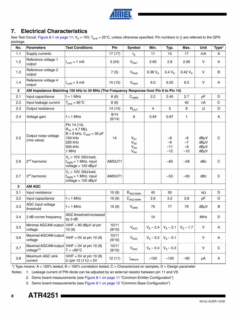
7. Electrical CharacteristicsSee Test Circuit, Figure 8-1 on page 11; VS = 10V, Tamb = 25°C, unless otherwise specified. Pin numbers in () are referred to the QFN package.
No. Parameters Test Conditions Pin Symbol Min. Typ. Max. Unit Type*
1.1 Supply currents 17 (17) IS 11 14 17 mA A
1.2Reference voltage 1 output
Ivref1 = 1 mA 3 (24) VRef1 2.65 2.8 2.95 V A
1.3Reference voltage 2 output
7 (5) VRef2 0.38 VS 0.4 VS 0.42 VS V B
1.4Reference voltage 4 output
Ivref4 = 3 mA 15 (15) VRef4 6.0 6.25 6.5 V A
2 AM Impedance Matching 150 kHz to 30 MHz (The Frequency Response from Pin 8 to Pin 14)
2.1 Input capacitance f = 1 MHz 8 (6) CAMIN 2.2 2.45 2.7 pF D
2.2 Input leakage current Tamb = 85°C 8 (6) 40 nA C
2.3 Output resistance 14 (14) ROUT 4 5 8 Ω D
2.4 Voltage gain f = 1 MHz8/14
(6/14)A 0.94 0.97 1 A
2.5Output noise voltage (rms value)
Pin 14 (14), R78 = 4.7 MΩ,B = 9 kHz, CANT = 30 pF150 kHz200 kHz500 kHz1 MHz
14 VN1VN2 VN3VN4
–8–9
–11 –12
–6–7–9
–10
dBµVdBµV dBµV dBµV
C
2.6 2nd harmonicVs = 10V, 50Ω load, fAMIN = 1 MHz, input voltage = 120 dBµV
AMOUT1 –60 –58 dBc C
2.7 3rd harmonicVs = 10V, 50Ω load, fAMIN = 1 MHz, input voltage = 120 dBµV
AMOUT1 –53 –50 dBc C
3 AM AGC
3.1 Input resistance 10 (9) RAGCAMIN 40 50 kΩ D
3.2 Input capacitance f = 1 MHz 10 (9) CAGCAMIN 2.6 3.2 3.8 pF D
3.3AGC input voltage threshold
f = 1 MHz 10 (9) VAMth 75 77 79 dBµV B
3.4 3 dB corner frequencyAGC threshold increased by 3 dB
10 MHz D
3.5Minimal AGCAM output voltage
ViHF = 90 dBµV at pin 10 (9)
10/11 (9/10)
VAGC VS – 2.4 VS – 2.1 VS – 1.7 V A
3.6Maximal AGCAM output voltage
ViHF = 0V at pin 10 (9)10/11 (9/10)
VAGC VS – 0.2 VS – 0.1 V A
3.7Maximal AGCAM output voltage(1)
ViHF = 0V at pin 10 (9) T = +85°C
10/11 (9/10)
VAGC VS – 0.4 VS – 0.3 V C
3.8Maximum AGC sink current
ViHF = 0V at pin 10 (9)U (pin 12 (11)) = 2V
12 (11) IAMsink –150 –120 –90 µA A
*) Type means: A = 100% tested, B = 100% correlation tested, C = Characterized on samples, D = Design parameter
Notes: 1. Leakage current of PIN diode can be adjusted by an external resistor between pin 11 and VS
2. Demo board measurements (see Figure 8-1 on page 11 “Common Emitter Configuration”)
3. Demo board measurements (see Figure 9-1 on page 12 “Common Base Configuration”)
84913J–AUDR–10/09
ATR4251
ATR4251
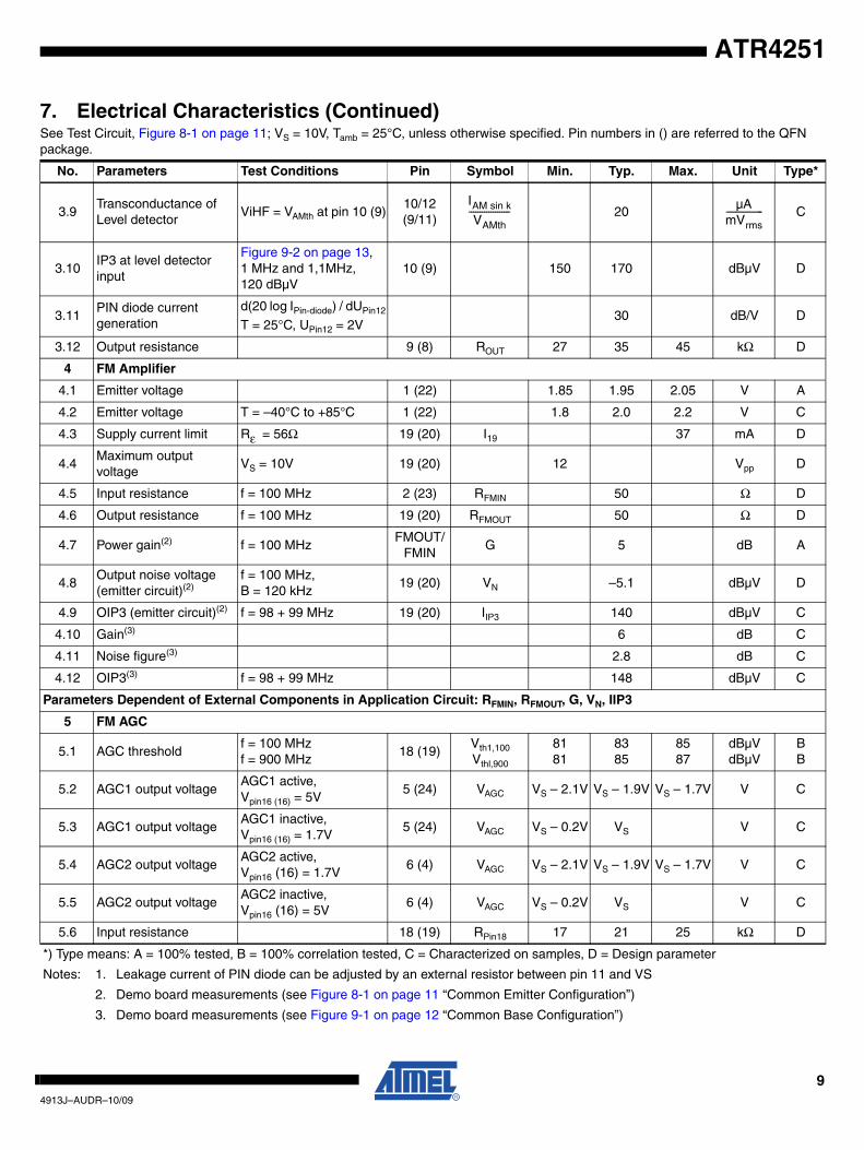
3.9Transconductance of Level detector
ViHF = VAMth at pin 10 (9)10/12 (9/11)
20 C
3.10IP3 at level detector input
Figure 9-2 on page 13, 1 MHz and 1,1MHz, 120 dBµV
10 (9) 150 170 dBµV D
3.11PIN diode current generation
d(20 log IPin-diode) / dUPin12
T = 25°C, UPin12 = 2V30 dB/V D
3.12 Output resistance 9 (8) ROUT 27 35 45 kΩ D
4 FM Amplifier
4.1 Emitter voltage 1 (22) 1.85 1.95 2.05 V A
4.2 Emitter voltage T = –40°C to +85°C 1 (22) 1.8 2.0 2.2 V C
4.3 Supply current limit Rε = 56Ω 19 (20) I19 37 mA D
4.4Maximum output voltage
VS = 10V 19 (20) 12 Vpp D
4.5 Input resistance f = 100 MHz 2 (23) RFMIN 50 Ω D
4.6 Output resistance f = 100 MHz 19 (20) RFMOUT 50 Ω D
4.7 Power gain(2) f = 100 MHzFMOUT/
FMING 5 dB A
4.8Output noise voltage (emitter circuit)(2)
f = 100 MHz, B = 120 kHz
19 (20) VN –5.1 dBµV D
4.9 OIP3 (emitter circuit)(2) f = 98 + 99 MHz 19 (20) IIP3 140 dBµV C
4.10 Gain(3) 6 dB C
4.11 Noise figure(3) 2.8 dB C
4.12 OIP3(3) f = 98 + 99 MHz 148 dBµV C
Parameters Dependent of External Components in Application Circuit: RFMIN, RFMOUT, G, VN, IIP3
5 FM AGC
5.1 AGC thresholdf = 100 MHzf = 900 MHz
18 (19)Vth1,100 Vthl,900
8181
8385
8587
dBµVdBµV
BB
5.2 AGC1 output voltageAGC1 active, Vpin16 (16) = 5V
5 (24) VAGC VS – 2.1V VS – 1.9V VS – 1.7V V C
5.3 AGC1 output voltageAGC1 inactive, Vpin16 (16) = 1.7V
5 (24) VAGC VS – 0.2V VS V C
5.4 AGC2 output voltageAGC2 active, Vpin16 (16) = 1.7V
6 (4) VAGC VS – 2.1V VS – 1.9V VS – 1.7V V C
5.5 AGC2 output voltageAGC2 inactive, Vpin16 (16) = 5V
6 (4) VAGC VS – 0.2V VS V C
5.6 Input resistance 18 (19) RPin18 17 21 25 kΩ D
7. Electrical Characteristics (Continued)See Test Circuit, Figure 8-1 on page 11; VS = 10V, Tamb = 25°C, unless otherwise specified. Pin numbers in () are referred to the QFN package.
No. Parameters Test Conditions Pin Symbol Min. Typ. Max. Unit Type*
*) Type means: A = 100% tested, B = 100% correlation tested, C = Characterized on samples, D = Design parameter
Notes: 1. Leakage current of PIN diode can be adjusted by an external resistor between pin 11 and VS
2. Demo board measurements (see Figure 8-1 on page 11 “Common Emitter Configuration”)
3. Demo board measurements (see Figure 9-1 on page 12 “Common Base Configuration”)
IAM sin k
VAMth------------------- µA
mVrms-----------------
94913J–AUDR–10/09

5.7 Input capacitance F = 100 MHz 18 (19) CPin18 1.5 1.75 1.9 pF D
5.8 IP3 at AGC inputFigure 9-2 on page 13, 100 MHz and 105 MHz, VGen = 120 dBµV
18 (19) 150 dBµV D
5.9 IP3 at AGC input900 MHz and 920 MHzVGen = 120 dBµV
18 (19) 148 dBµV D
5.10 Max. AGC sink current ViHF = 0V 16 IPin16 –11 –9 –7 µA C
5.11 Transconductance ViHF = Vth1,100, dIPin16(16) / dUPin18(19)
dIPin16 / dUPin18
0.8 1.0 1.3mA/V (rms)
C
5.12 Gain AGC1, AGC2UPin16 = 3V, dUPin5(3) / dUPin16(16), –dUPin6(4) / dUPin16(16)
0.5 0.56 0.6 C
7. Electrical Characteristics (Continued)See Test Circuit, Figure 8-1 on page 11; VS = 10V, Tamb = 25°C, unless otherwise specified. Pin numbers in () are referred to the QFN package.
No. Parameters Test Conditions Pin Symbol Min. Typ. Max. Unit Type*
*) Type means: A = 100% tested, B = 100% correlation tested, C = Characterized on samples, D = Design parameter
Notes: 1. Leakage current of PIN diode can be adjusted by an external resistor between pin 11 and VS
2. Demo board measurements (see Figure 8-1 on page 11 “Common Emitter Configuration”)
3. Demo board measurements (see Figure 9-1 on page 12 “Common Base Configuration”)
104913J–AUDR–10/09
ATR4251

ATR4251
8. Test Circuit FM/AM
Figure 8-1. Common Emitter Configuration
FM
IN
VR
EF
1
GN
D
AG
C1
AG
C2
AG
CA
MIN
CR
EG
AM
IN1
VR
EF
2
FM
GA
IN
2 3 4 5 6 109871
FM
OU
T
AG
CIN
VS
AG
CC
ON
ST
VR
EF
4
AG
CA
M
TC
ON
ST
GN
D1
AM
OU
T1
GN
D2
19 18 17 16
AG
C(A
M)
Ban
dga
p
AG
C
SS
O20
FM
ampl
ifier
15 1112131420
1 nF
AM
+
+ +
+
+
22 pF150 nH
100 nF
2.2 nF
2.2 nF
2.2 nF
220 nF33 pF 15 nF
Cant
1 µF
1 µH
10 µF
10 µF
AGCIN
AMOUT1
AMINP1 AMAGCIN
GND
FMOUT
FMIN
VS
47Ω1)
4.7Ω
270Ω
56Ω
50Ω
68Ω
4.7 MΩ
22Ω
5 kΩ
4.7 µF 2.2 µF
+
100 nF
22 pF
2.2 nF
10 µF
4.7Ω
470 nF 500 pF
50Ω
(1) Output impedance 50Ω adjustment
114913J–AUDR–10/09

9. Application Circuit (Demo Board)
Figure 9-1. Common Base Configuration
FM
IN
VR
EF
1
GN
D
AG
C1
AG
C2
AG
CA
MIN
CR
EG
AM
IN1
VR
EF
2
FM
GA
IN
2 3 4 5 6 109871
FM
OU
T
AG
CIN
VS
AG
CC
ON
ST
VR
EF
4
AG
CA
M
TC
ON
ST
GN
D1
AM
OU
T1
GN
D2
19 18 17 16
AG
C(A
M)
Ban
dga
p
AG
C
SS
O20
FM
ampl
ifier
15 1112131420
1 nF
2.2 µF
AM
+
1 pF(4)
1 pF
10 nF
R11(2)
(2)
(2)
R12(2)
2.2 pF (4)
C18
C28
C1
C6
C20
C19
C17
33 pFC31
C13
C21
100 nF
C30C26 C23
C27 C24
D3
BA779-2
R21
R7
R3
1 kΩ
R23
R9
R24
470 nH
470 nF
220 nF
L3
120 nHL1
BC858T2
180 nH
L3
100 nF
2.2 pF
C2
C29
2.2 nF
2.2 nF
C5
2.2 nF C4
22 pF
C3 C7
C10
15 nF
C32
100 nF
TR1
T1
BC858
6 4
1 3
220 nF
1 µF
C8
1 nF
10 µFGND
2. Testing AM + AM AGCconnector AM as inputconnector AM/FM_OUT as output
1. Testing FM + FM AGCconnector FM as inputconnector AM/FM_OUT as output
(2) Leakage current reduction
(3) AM AGC threshold
(4) AM AGC threshold
(1) AM Output impedance (50Ω adjustment)
AM/FM application combined with AM AGCwith the following capability
AM
FM
AM/FM_OUT
VB+ 10
+VS
+VS
+VS
4.7Ω
4.7 MΩ
51ΩR2
D1
BA679BA679
D2
100Ω
68Ω
R5
R4
R25
R8
R6
2ΩRS1
47ΩR1
100Ω
R10100Ω10 kΩ
2.2 kΩ
R20
33Ω(1)
3 kΩ(3)
10 kΩ(3)
+
+
+
100 nF
100 pF
C11
10 µF
10 µF
4.7 µF
4.7Ω
100 nF
C12
C33
124913J–AUDR–10/09
ATR4251
ATR4251
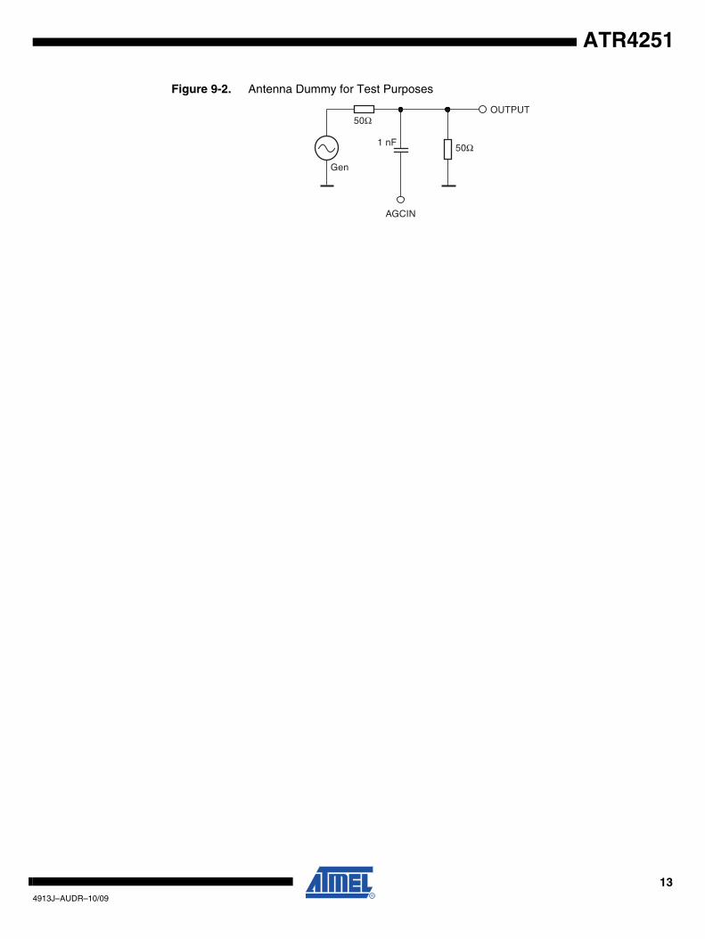
Figure 9-2. Antenna Dummy for Test Purposes
OUTPUT
AGCIN
Gen
1 nF
50Ω
50Ω
134913J–AUDR–10/09

10. Internal Circuitry
Table 10-1. Equivalent Pin Circuits (ESD Protection Circuits Not Shown)
PIN SSO20 PIN QFN24 Symbol Equivalent Circuit
12
19
222320
FMGAINFMIN
FMOUT
3 24 VREF1
4, 13, 20 2, 13, 21 GND
56
34
AGC1AGC2
1, 7, 12, 18 NC
7 5 VREF2
19
1
2
3
5
VS
7
144913J–AUDR–10/09
ATR4251

ATR4251
8 6 AMIN1
9 8 CREG
10 9 AGCAMIN
11 10 AGCAM
Table 10-1. Equivalent Pin Circuits (ESD Protection Circuits Not Shown) (Continued)
PIN SSO20 PIN QFN24 Symbol Equivalent Circuit
8
VS
9
10
11
154913J–AUDR–10/09

12 11 TCONS
14 14 AMOUT1
15 15 VREF4
16 16 AGCCONST
17 17 VS
Table 10-1. Equivalent Pin Circuits (ESD Protection Circuits Not Shown) (Continued)
PIN SSO20 PIN QFN24 Symbol Equivalent Circuit
12
14
15
16
164913J–AUDR–10/09
ATR4251

ATR4251
18 19 AGCIN
Table 10-1. Equivalent Pin Circuits (ESD Protection Circuits Not Shown) (Continued)
PIN SSO20 PIN QFN24 Symbol Equivalent Circuit
18
174913J–AUDR–10/09

12. Package Information
Figure 12-1. SSO20
11. Ordering InformationExtended Type Number Package Remarks MOQ
ATR4251-TKSY SSO20 Sticks 830 pieces
ATR4251-TKQY SSO20 Taped and reeled 4000 pieces
ATR4251-PFQY QFN24, 4 mm × 4 mm Taped and reeled 6000 pieces
ATR4251-PFPY QFN24, 4 mm × 4 mm Taped and reeled 1500 pieces
Package: SSO20Dimensions in mm
specificationsaccording to DINtechnical drawings
6.75-0.25
1120
101
Issue: 1; 10.03.04
Drawing-No.: 6.543-5056.01-4
5.85±0.05
1.3±
0.05
0.15
±0.
05
0.65±0.05
5.4±0.2
4.4±0.1
6.45±0.150.25±0.05
0.05
+0.
1
184913J–AUDR–10/09
ATR4251
ATR4251
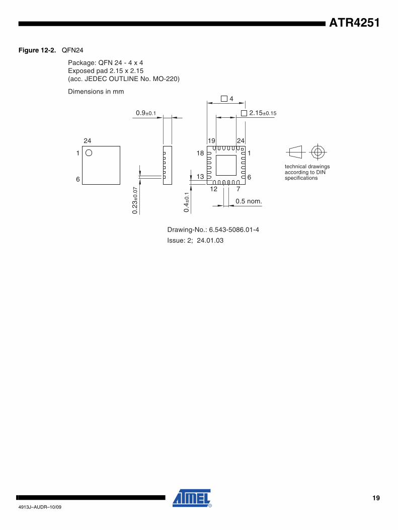
Figure 12-2. QFN24
0.23
±0.
07
0.4±
0.1
0.9±0.1 2.15±0.15
712
2419
13
18
6
1
24
6
1
4
0.5 nom.
Package: QFN 24 - 4 x 4 Exposed pad 2.15 x 2.15(acc. JEDEC OUTLINE No. MO-220)
Dimensions in mm
specificationsaccording to DINtechnical drawings
Issue: 2; 24.01.03
Drawing-No.: 6.543-5086.01-4
194913J–AUDR–10/09

13. Revision History
Please note that the following page numbers referred to in this section refer to the specific revision mentioned, not to this document.
Revision No. History
4913J-AUDR-10/09 • Section 11 “Ordering Information” on page 18 changed
4913I-AUDR-03/08
• Figure 1-1 “Block Diagram QFN24 Package” on page 1 changed
• Figure 2-1 “Pinning QFN24” on page 3 changed• Table 2-1 “Pin Description QFN24” on page 3 changed
• Table 10-1 “Equivalent Pin Circuits (ESD Protection Circuits Not Shown) on page 14 changed
• Section 11 “Ordering Information” on page 18 changed
4913H-AUDR-10/07
• Section 7 “Electrical Characteristics” numbers 1.1, 1.2, 1.3, 1.4, 2.4, 3.5, 3.6, 4.3 and 5.1 on pages 8 to 9 changed
• Section 7 “Electrical Characteristics” numbers 2.8 and 2.9 deleted
• Figure 8-1 “Common Emitter Configuration” on page 11 changed
4913G-AUDR-07/07• Figure 8-1 “Common Emitter Configuration” on page 11 changed• Figure 9-1 “Common Base Configuration” on page 12 changed
4913F-AUDR-06/07
• Put datasheet in a new template
• Figure 8-1 “Common Emitter Configuration” on page 11 changed
• Figure 8-1 “Common Base Configuration” on page 12 changed
4913E-AUDR-02/07
• Put datasheet in a new template• Figure 1-1 exchanged with figure 1-2 on pages 1 to 2
• Figure 2-1 exchanged with figure 2-2 on pages 3 to 4
• Table 2-1 exchanged with table 2-2 on pages 3 to 4
• Section 3.1 “AM Amplifier” on page 5 changed• Section 3.4 “FM AGC” on page 6 renamed in “FM/TV AGC” and changed
• Section 7 “Electrical Characteristics” on pages 8 to 10 changed
• Figure 9-1 “Common Base Configuration” on page 12 changed
204913J–AUDR–10/09
ATR4251

4913J–AUDR–10/09
Headquarters International
Atmel Corporation2325 Orchard ParkwaySan Jose, CA 95131USATel: 1(408) 441-0311Fax: 1(408) 487-2600
Atmel AsiaUnit 1-5 & 16, 19/FBEA Tower, Millennium City 5418 Kwun Tong RoadKwun Tong, KowloonHong KongTel: (852) 2245-6100Fax: (852) 2722-1369
Atmel EuropeLe Krebs8, Rue Jean-Pierre TimbaudBP 30978054 Saint-Quentin-en-Yvelines CedexFranceTel: (33) 1-30-60-70-00 Fax: (33) 1-30-60-71-11
Atmel Japan9F, Tonetsu Shinkawa Bldg.1-24-8 ShinkawaChuo-ku, Tokyo 104-0033JapanTel: (81) 3-3523-3551Fax: (81) 3-3523-7581
Product Contact
Web Sitewww.atmel.com
Technical [email protected]
Sales Contactwww.atmel.com/contacts
Literature Requestswww.atmel.com/literature
Disclaimer: The information in this document is provided in connection with Atmel products. No license, express or implied, by estoppel or otherwise, to anyintellectual property right is granted by this document or in connection with the sale of Atmel products. EXCEPT AS SET FORTH IN ATMEL’S TERMS AND CONDI-TIONS OF SALE LOCATED ON ATMEL’S WEB SITE, ATMEL ASSUMES NO LIABILITY WHATSOEVER AND DISCLAIMS ANY EXPRESS, IMPLIED OR STATUTORYWARRANTY RELATING TO ITS PRODUCTS INCLUDING, BUT NOT LIMITED TO, THE IMPLIED WARRANTY OF MERCHANTABILITY, FITNESS FOR A PARTICULARPURPOSE, OR NON-INFRINGEMENT. IN NO EVENT SHALL ATMEL BE LIABLE FOR ANY DIRECT, INDIRECT, CONSEQUENTIAL, PUNITIVE, SPECIAL OR INCIDEN-TAL DAMAGES (INCLUDING, WITHOUT LIMITATION, DAMAGES FOR LOSS OF PROFITS, BUSINESS INTERRUPTION, OR LOSS OF INFORMATION) ARISING OUT OFTHE USE OR INABILITY TO USE THIS DOCUMENT, EVEN IF ATMEL HAS BEEN ADVISED OF THE POSSIBILITY OF SUCH DAMAGES. Atmel makes norepresentations or warranties with respect to the accuracy or completeness of the contents of this document and reserves the right to make changes to specificationsand product descriptions at any time without notice. Atmel does not make any commitment to update the information contained herein. Unless specifically providedotherwise, Atmel products are not suitable for, and shall not be used in, automotive applications. Atmel’s products are not intended, authorized, or warranted for useas components in applications intended to support or sustain life.
© 2009 Atmel Corporation. All rights reserved. Atmel®, logo and combinations thereof, and others are registered trademarks or trademarks ofAtmel Corporation or its subsidiaries. Other terms and product names may be trademarks of others.


