Low-Dimensional Te … Te-Based Nanostructures ... Low-dimensional nanomaterials, ... This article...
7
© 2013 WILEY-VCH Verlag GmbH & Co. KGaA, Weinheim 3915 www.advmat.de www.MaterialsViews.com wileyonlinelibrary.com RESEARCH NEWS Low-Dimensional Te-Based Nanostructures Qisheng Wang, Muhammad Safdar, Zhenxing Wang, and Jun He* 1. Introduction Low-dimensional nanomaterials, with at least one physical dimension constrained to the nanometer scale, have attracted huge attention during the last few decades. Owing to their sur- face effect, quantum size effect, and macroscopic quantum-tun- neling effect, low-dimensional nanomaterials exhibit superior properties to those of their bulk counterparts and have opened up new and sometimes unexpected fields of applications in nanoscale electronic and optoelectronic devices such as ZnO- nanowire-based nanogenerators, [1] reduced graphene oxide field-effect-transistor (FET)-based biosensors, [2] CdS/Cu 2 S- core–shell nanowire-based solar cells, [3] and ZnSe-nanobelt- based photodetectors. [4] High-quality single-crystalline low-dimensional Te-based nanomaterials show fascinating surface-state properties: photo- electricity, phase-change memory, and thermoelectricity, owing to intrinsic novel properties of their bulk counterparts [5] and the unique morphology of their low-dimensional nanostructures. For example, due to crystal defects or environmental doping in a bulk topological insulator, contribution of the surface carriers to the charge-transport measurement is always masked in bulk materials. However, one- and two-dimensional Te-based nano- structures, such as Ag 2 Te, [6] Bi 2 Te 3 , [7] and Sb 2 Te 3 , [8] with large surface-to-volume ratios, strengthen electron transmission on the surface; this results in the successful observation of sur- face electronic properties. The one-dimensional (1D) ZnTe, [9] CdTe, [10] and In 2 Te 3 [11] nanostructure also shows enhanced photoelectrical performance such as high quantum efficiency due to the surface effect and high crystallinity of the 1D nanostructure. In addition, 1D GeTe-, [12] Sb 2 Te 3 -, [13] and Ge 2 Sb 2 Te 5 -based [14] phase- change memory devices show low power dissipation due to the lower melting point of the nanowire than of the bulk materials. Furthermore, a 1D PbTe-based thermo- electric material, which has the advantages of both quantum confinement to enhance the power factor and phonon scattering at the nanostructure surface to lower thermal conductivity, shows a much higher ther- moelectric figure of merit (ZT). [15] Thanks to the successful development of various growth methods such as van der Waals epitaxial growth, [16] Au-catalyzed vapor–liquid–solid deposition, [6] and template-directed growth, [17] high-quality and single-crystalline low-dimensional Te-based nanomaterials have been obtained, which pave the way for the observation of novel physical prop- erties. This article reviews recent development in the synthesis, properties, and applications of low-dimensional Te-based nanostructures. 2. Synthesis of Single-Crystalline Te-Based Nanostructures Controllable synthesis of high-quality and -mass single-crystal- line low-dimensional nanomaterials is very important for the exhibition of novel physical performance of nanoscale electronic and photoelectronic devices. In recent years, systematic synthesis technologies have been developed and successfully used for the growth of low-dimensional Te-based nanostructures, such as vapor-phase deposition, [16] the solvothermal method, [18] and the electrochemical deposition method. [19] Specifically, some unique growth mechanisms have been applied to synthesize Te-based nanomaterials, for example, van der Waals epitaxial growth of few-layer Bi 2 Te 3 nanoplates, [16] and Au-catalyzed vapor–liquid– solid growth of single-crystalline β-Ag 2 Te nanowires. [20] 2.1. Vapor-Phase Deposition Methods In layered-structure Bi 2 Te 3 and Sb 2 Te 3 , the quintuple layers (QLs) weakly interact by means of van der Waals forces. There- fore, the vapor–solid (VS) method is particularly suitable for growth of two-dimensional (2D) Sb 2 Te 3 and Bi 2 Te 3 nanostruc- tures. Few-layer Sb 2 Te 3 nanoplates have been successfully syn- thesized on various substrates such as SiO 2 /Si, Si (111), and Low-dimensional Te-based nanomaterials have attracted intense attention in recent years due to their novel physical properties including surface-state effects, photoelectricity, phase changes, and thermoelectricity. The recent development of synthesis methods of low-dimensional Te-based nanostruc- tures is reviewed, such as van der Waals expitaxial growth and template- assisted solution-phase deposition. In addition, the unique properties of these materials, such as tunable surface states, high photoresponsivity, fast phase change, and high thermoelectricity figure of merit, are reviewed. The potential applications of low-dimensional Te-based nanostructures are broad but particularly promising for nanoscale electronic and photoelectronic devices. Q. Wang, M. Safdar, Dr. Z. Wang, Prof. J. He National Center for Nanoscience and Technology Beijing 100190, P. R. China E-mail: [email protected] DOI: 10.1002/adma.201301128 Adv. Mater. 2013, 25, 3915–3921
-
Upload
vuongduong -
Category
Documents
-
view
224 -
download
0
Transcript of Low-Dimensional Te … Te-Based Nanostructures ... Low-dimensional nanomaterials, ... This article...

www.advmat.dewww.MaterialsViews.com
RES
EAR
Low-Dimensional Te-Based Nanostructures
Qisheng Wang , Muhammad Safdar , Zhenxing Wang , and Jun He *
CH N
EWS
Low-dimensional Te-based nanomaterials have attracted intense attention in recent years due to their novel physical properties including surface-state effects, photoelectricity, phase changes, and thermoelectricity. The recent development of synthesis methods of low-dimensional Te-based nanostruc-tures is reviewed, such as van der Waals expitaxial growth and template-assisted solution-phase deposition. In addition, the unique properties of these materials, such as tunable surface states, high photoresponsivity, fast phase change, and high thermoelectricity fi gure of merit, are reviewed. The potential applications of low-dimensional Te-based nanostructures are broad but particularly promising for nanoscale electronic and photoelectronic devices.
1. Introduction
Low-dimensional nanomaterials, with at least one physical dimension constrained to the nanometer scale, have attracted huge attention during the last few decades. Owing to their sur-face effect, quantum size effect, and macroscopic quantum-tun-neling effect, low-dimensional nanomaterials exhibit superior properties to those of their bulk counterparts and have opened up new and sometimes unexpected fi elds of applications in nanoscale electronic and optoelectronic devices such as ZnO-nanowire-based nanogenerators, [ 1 ] reduced graphene oxide fi eld-effect-transistor (FET)-based biosensors, [ 2 ] CdS/Cu 2 S-core–shell nanowire-based solar cells, [ 3 ] and ZnSe-nanobelt-based photodetectors. [ 4 ]
High-quality single-crystalline low-dimensional Te-based nanomaterials show fascinating surface-state properties: photo-electricity, phase-change memory, and thermoelectricity, owing to intrinsic novel properties of their bulk counterparts [ 5 ] and the unique morphology of their low-dimensional nanostructures. For example, due to crystal defects or environmental doping in a bulk topological insulator, contribution of the surface carriers to the charge-transport measurement is always masked in bulk materials. However, one- and two-dimensional Te-based nano-structures, such as Ag 2 Te, [ 6 ] Bi 2 Te 3 , [ 7 ] and Sb 2 Te 3 , [ 8 ] with large surface-to-volume ratios, strengthen electron transmission on the surface; this results in the successful observation of sur-face electronic properties. The one-dimensional (1D) ZnTe, [ 9 ] CdTe, [ 10 ] and In 2 Te 3 [ 11 ] nanostructure also shows enhanced
© 2013 WILEY-VCH Verlag GmbH & Co. KGaA, Weinheim
Q. Wang, M. Safdar, Dr. Z. Wang, Prof. J. HeNational Center for Nanoscience and Technology Beijing 100190, P. R. China E-mail: [email protected]
DOI: 10.1002/adma.201301128
Adv. Mater. 2013, 25, 3915–3921
photoelectrical performance such as high quantum effi ciency due to the surface effect and high crystallinity of the 1D nanostructure. In addition, 1D GeTe-, [ 12 ] Sb 2 Te 3 -, [ 13 ] and Ge 2 Sb 2 Te 5 -based [ 14 ] phase-change memory devices show low power dissipation due to the lower melting point of the nanowire than of the bulk materials. Furthermore, a 1D PbTe-based thermo-electric material, which has the advantages of both quantum confi nement to enhance the power factor and phonon scattering at the nanostructure surface to lower thermal conductivity, shows a much higher ther-moelectric fi gure of merit (ZT). [ 15 ]
Thanks to the successful development
of various growth methods such as van der Waals epitaxial growth, [ 16 ] Au-catalyzed vapor–liquid–solid deposition, [ 6 ] and template-directed growth, [ 17 ] high-quality and single-crystalline low-dimensional Te-based nanomaterials have been obtained, which pave the way for the observation of novel physical prop-erties. This article reviews recent development in the synthesis, properties, and applications of low-dimensional Te-based nanostructures.2. Synthesis of Single-Crystalline Te-Based Nanostructures
Controllable synthesis of high-quality and -mass single-crystal-line low-dimensional nanomaterials is very important for the exhibition of novel physical performance of nanoscale electronic and photoelectronic devices. In recent years, systematic synthesis technologies have been developed and successfully used for the growth of low-dimensional Te-based nanostructures, such as vapor-phase deposition, [ 16 ] the solvothermal method, [ 18 ] and the electrochemical deposition method. [ 19 ] Specifi cally, some unique growth mechanisms have been applied to synthesize Te-based nanomaterials, for example, van der Waals epitaxial growth of few-layer Bi 2 Te 3 nanoplates, [ 16 ] and Au-catalyzed vapor–liquid–solid growth of single-crystalline β -Ag 2 Te nanowires. [ 20 ]
2.1. Vapor-Phase Deposition Methods
In layered-structure Bi 2 Te 3 and Sb 2 Te 3 , the quintuple layers (QLs) weakly interact by means of van der Waals forces. There-fore, the vapor–solid (VS) method is particularly suitable for growth of two-dimensional (2D) Sb 2 Te 3 and Bi 2 Te 3 nanostruc-tures. Few-layer Sb 2 Te 3 nanoplates have been successfully syn-thesized on various substrates such as SiO 2 /Si, Si (111), and
3915wileyonlinelibrary.com
391
www.advmat.dewww.MaterialsViews.com
RES
EARCH N
EWS
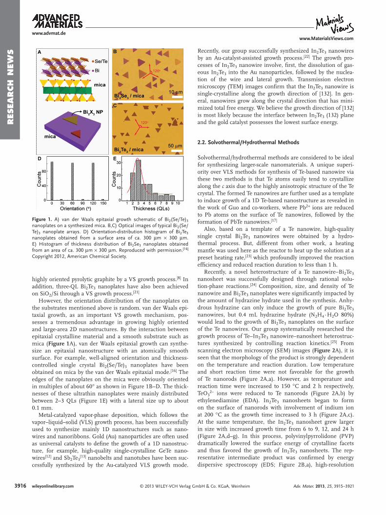
Figure 1 . A) van der Waals epitaxial growth schematic of Bi 2 (Se/Te) 3 nano plates on a synthesized mica. B,C) Optical images of typical Bi 2 (Se/Te) 3 nanoplate arrays. D) Orientation-distribution histogram of Bi 2 Te 3 nanoplates obtained from a surface area of ca. 300 μ m × 300 μ m. E) Histogram of thickness distribution of Bi 2 Se 3 nanoplates obtained from an area of ca. 300 μ m × 300 μ m. Reproduced with permission. [ 16 ] Copyright 2012, American Chemical Society.
highly oriented pyrolytic graphite by a VS growth process. [ 8 ] In addition, three-QL Bi 2 Te 3 nanoplates have also been achieved on SiO 2 /Si through a VS growth process. [ 21 ]
However, the orientation distribution of the nanoplates on the substrates mentioned above is random. van der Waals epi-taxial growth, as an important VS growth mechanism, pos-sesses a tremendous advantage in growing highly oriented and large-area 2D nanostructures. By the interaction between epitaxial crystalline material and a smooth substrate such as mica ( Figure 1 A), van der Waals epitaxial growth can synthe-size an epitaxial nanostructure with an atomically smooth surface. For example, well-aligned orientation and thickness-controlled single crystal Bi 2 (Se/Te) 3 nanoplates have been obtained on mica by the van der Waals epitaxial mode. [ 16 ] The edges of the nanoplates on the mica were obviously oriented in multiples of about 60 ° as shown in Figure 1 B–D. The thick-nesses of these ultrathin nanoplates were mainly distributed between 2–3 QLs (Figure 1 E) with a lateral size up to about 0.1 mm.
Metal-catalyzed vapor-phase deposition, which follows the vapor–liquid–solid (VLS) growth process, has been successfully used to synthesize mainly 1D nanostructures such as nano-wires and nanoribbons. Gold (Au) nanoparticles are often used as universal catalysts to defi ne the growth of a 1D nanostruc-ture, for example, high-quality single-crystalline GeTe nano-wires [ 12 ] and Sb 2 Te 3 [ 13 ] nanobelts and nanotubes have been suc-cessfully synthesized by the Au-catalyzed VLS growth mode.
6 wileyonlinelibrary.com © 2013 WILEY-VCH Verlag G
Recently, our group successfully synthesized In 2 Te 3 nanowires by an Au-catalyst-assisted growth process. [ 22 ] The growth pro-cesses of In 2 Te 3 nanowire involve, fi rst, the dissolution of gas-eous In 2 Te 3 into the Au nanoparticles, followed by the nuclea-tion of the wire and lateral growth. Transmission electron microscopy (TEM) images confi rm that the In 2 Te 3 nanowire is single-crystalline along the growth direction of [132]. In gen-eral, nanowires grow along the crystal direction that has mini-mized total free energy. We believe the growth direction of [132] is most likely because the interface between In 2 Te 3 (132) plane and the gold catalyst possesses the lowest surface energy.
2.2. Solvothermal/Hydrothermal Methods
Solvothermal/hydrothermal methods are considered to be ideal for synthesizing larger-scale nanomaterials. A unique superi-ority over VLS methods for synthesis of Te-based nanowire via these two methods is that Te atoms easily tend to crystallize along the c axis due to the highly anisotropic structure of the Te crystal. The formed Te nanowires are further used as a template to induce growth of a 1D Te-based nanostructure as revealed in the work of Guo and co-workers, where Pb 2 + ions are reduced to Pb atoms on the surface of Te nanowires, followed by the formation of PbTe nanowires. [ 17 ]
Also, based on a template of a Te nanowire, high-quality single crystal Bi 2 Te 3 nanowires were obtained by a hydro-thermal process. But, different from other work, a heating mantle was used here as the reactor to heat up the solution at a preset heating rate, [ 23 ] which profoundly improved the reaction effi ciency and reduced reaction duration to less than 1 h.
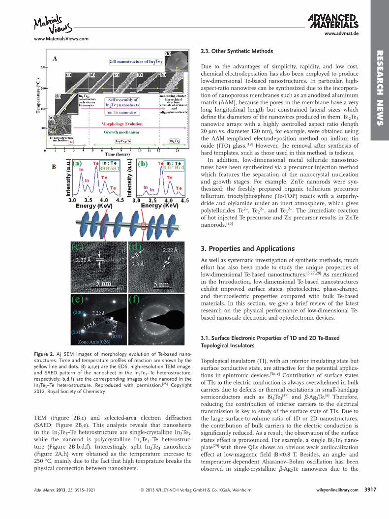
Recently, a novel heterostructure of a Te nanowire–Bi 2 Te 3 nanosheet was successfully designed through rational solu-tion-phase reactions. [ 24 ] Composition, size, and density of Te nanowire and Bi 2 Te 3 nanoplates were signifi cantly impacted by the amount of hydrazine hydrate used in the synthesis. Anhy-drous hydrazine can only induce the growth of pure Bi 2 Te 3 nanowires, but 0.4 mL hydrazine hydrate (N 2 H 4 · H 2 O 80%) would lead to the growth of Bi 2 Te 3 nanoplates on the surface of the Te nanowires. Our group systematically researched the growth process of Te–In 2 Te 3 nanowire–nanosheet heterostruc-tures synthesized by controlling reaction kinetics. [ 25 ] From scanning electron microscopy (SEM) images ( Figure 2 A), it is seen that the morphology of the product is strongly dependent on the temperature and reaction duration. Low temperature and short reaction time were not favorable for the growth of Te nanorods (Figure 2 A,a). However, as temperature and reaction time were increased to 150 ° C and 2 h respectively, TeO 3 2– ions were reduced to Te nanorods (Figure 2 A,b) by ethylenediamine (EDA). In 2 Te 3 nanosheets began to form on the surface of nanorods with involvement of indium ion at 200 ° C as the growth time increased to 3 h (Figure 2 A,c). At the same temperature, the In 2 Te 3 nanosheet grew larger in size with increased growth time from 6 to 9, 12, and 24 h (Figure 2 A,d–g). In this process, polyvinylpyrrolidone (PVP) dramatically lowered the surface energy of crystalline facets and thus favored the growth of In 2 Te 3 nanosheets. The rep-resentative intermediate product was confi rmed by energy dispersive spectroscopy (EDS; Figure 2 B,a), high-resolution
mbH & Co. KGaA, Weinheim Adv. Mater. 2013, 25, 3915–3921
www.advmat.dewww.MaterialsViews.com
RES
EARCH N
EWS
Figure 2 . A) SEM images of morphology evolution of Te-based nano-structures. Time and temperature profi les of reaction are shown by the yellow line and dots. B) a,c,e) are the EDS, high-resolution TEM image, and SAED pattern of the nanosheet in the In 2 Te 3 –Te heterostructure, respectively; b,d,f) are the corresponding images of the nanorod in the In 2 Te 3 –Te heterostructure. Reproduced with permission. [ 25 ] Copyright 2012, Royal Society of Chemistry.
TEM (Figure 2 B,c) and selected-area electron diffraction (SAED; Figure 2 B,e). This analysis reveals that nanosheets in the In 2 Te 3 –Te heterostructure are single-crystalline In 2 Te 3 , while the nanorod is polycrystalline In 2 Te 3 –Te heterostruc-ture (Figure 2 B,b,d,f). Interestingly, split In 2 Te 3 nanosheets (Figure 2 A,h) were obtained as the temperature increase to 250 ° C, mainly due to the fact that high temprature breaks the physical connection between nanosheets.
© 2013 WILEY-VCH Verlag GAdv. Mater. 2013, 25, 3915–3921
2.3. Other Synthetic Methods
Due to the advantages of simplicity, rapidity, and low cost, chemical electrodeposition has also been employed to produce low-dimensional Te-based nanostructures. In particular, high-aspect-ratio nanowires can be synthesized due to the incorpora-tion of nanoporous membranes such as an anodized aluminum matrix (AAM), because the pores in the membrane have a very long longitudinal length but constrained lateral sizes which defi ne the diameters of the nanowires produced in them. Bi 2 Te 3 nanowire arrays with a highly controlled aspect ratio (length 20 μ m vs. diameter 120 nm), for example, were obtained using the AAM-templated electrodeposition method on indium–tin oxide (ITO) glass. [ 19 ] However, the removal after synthesis of hard templates, such as those used in this method, is tedious.
In addition, low-dimensional metal telluride nanostruc-tures have been synthesized via a precursor injection method which features the separation of the nanocrystal nucleation and growth stages. For example, ZnTe nanorods were syn-thesized; the freshly prepared organic tellurium precursor tellurium trioctylphosphine (Te-TOP) reacts with a superhy-dride and olylamide under an inert atmosphere, which gives polytellurides Te 2 − , Te 2 2 − , and Te 3 2 − . The immediate reaction of hot injected Te precursor and Zn precursor results in ZnTe nanorods. [ 26 ]
3. Properties and Applications
As well as systematic investigation of synthetic methods, much effort has also been made to study the unique properties of low-dimensional Te-based nanostructures. [ 6 , 27,28 ] As mentioned in the Introduction, low-dimensional Te-based nanostructures exhibit improved surface states, photoelectric, phase-change, and thermoelectric properties compared with bulk Te-based materials. In this section, we give a brief review of the latest research on the physical performance of low-dimensional Te-based nanoscale electronic and optoelectronic devices.
3.1. Surface Electronic Properties of 1D and 2D Te-Based Topological Insulators
Topological insulators (TI), with an interior insulating state but surface conductive state, are attractive for the potential applica-tions in spintronic devices. [ 5a–c ] Contribution of surface states of TIs to the electric conduction is always overwhelmed in bulk carriers due to defects or thermal excitations in small-bandgap semiconductors such as Bi 2 Te 3 [ 27 ] and β -Ag 2 Te. [ 6 ] Therefore, reducing the contribution of interior carriers to the electrical transmission is key to study of the surface state of TIs. Due to the large surface-to-volume ratio of 1D or 2D nanostructures, the contribution of bulk carriers to the electric conduction is signifi cantly reduced. As a result, the observation of the surface states effect is pronounced. For example, a single Bi 2 Te 3 nano-plate [ 29 ] with three QLs shows an obvious weak antilocalization effect at low-magnetic fi eld | B | < 0.8 T. Besides, an angle- and temperature-dependent Aharanov–Bohm oscillation has been observed in single-crystalline β -Ag 2 Te nanowires due to the
3917wileyonlinelibrary.commbH & Co. KGaA, Weinheim
39
www.advmat.dewww.MaterialsViews.com
RES
EARCH N
EWS
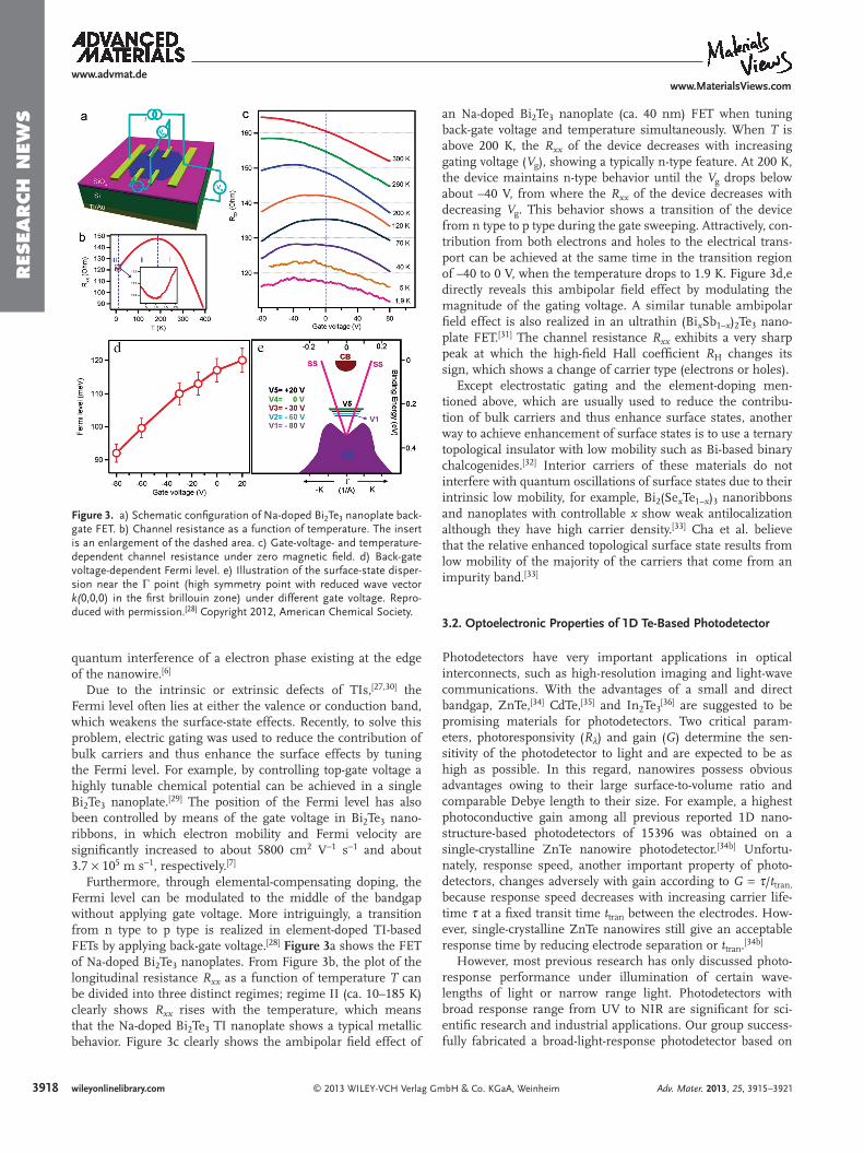
Figure 3 . a) Schematic confi guration of Na-doped Bi 2 Te 3 nanoplate back-gate FET. b) Channel resistance as a function of temperature. The insert is an enlargement of the dashed area. c) Gate-voltage- and temperature-dependent channel resistance under zero magnetic fi eld. d) Back-gate voltage-dependent Fermi level. e) Illustration of the surface-state disper-sion near the Γ point (high symmetry point with reduced wave vector k( 0,0,0) in the fi rst brillouin zone) under different gate voltage. Repro-duced with permission. [ 28 ] Copyright 2012, American Chemical Society.
quantum interference of a electron phase existing at the edge of the nanowire. [ 6 ]
Due to the intrinsic or extrinsic defects of TIs, [ 27 , 30 ] the Fermi level often lies at either the valence or conduction band, which weakens the surface-state effects. Recently, to solve this problem, electric gating was used to reduce the contribution of bulk carriers and thus enhance the surface effects by tuning the Fermi level. For example, by controlling top-gate voltage a highly tunable chemical potential can be achieved in a single Bi 2 Te 3 nanoplate. [ 29 ] The position of the Fermi level has also been controlled by means of the gate voltage in Bi 2 Te 3 nano-ribbons, in which electron mobility and Fermi velocity are signifi cantly increased to about 5800 cm 2 V − 1 s − 1 and about 3.7 × 10 5 m s − 1 , respectively. [ 7 ]
Furthermore, through elemental-compensating doping, the Fermi level can be modulated to the middle of the bandgap without applying gate voltage. More intriguingly, a transition from n type to p type is realized in element-doped TI-based FETs by applying back-gate voltage. [ 28 ] Figure 3 a shows the FET of Na-doped Bi 2 Te 3 nanoplates. From Figure 3 b, the plot of the longitudinal resistance R xx as a function of temperature T can be divided into three distinct regimes; regime II (ca. 10–185 K) clearly shows R xx rises with the temperature, which means that the Na-doped Bi 2 Te 3 TI nanoplate shows a typical metallic behavior. Figure 3 c clearly shows the ambipolar fi eld effect of
18 wileyonlinelibrary.com © 2013 WILEY-VCH Verlag G
an Na-doped Bi 2 Te 3 nanoplate (ca. 40 nm) FET when tuning back-gate voltage and temperature simultaneously. When T is above 200 K, the R xx of the device decreases with increasing gating voltage ( V g ), showing a typically n-type feature. At 200 K, the device maintains n-type behavior until the V g drops below about –40 V, from where the R xx of the device decreases with decreasing V g . This behavior shows a transition of the device from n type to p type during the gate sweeping. Attractively, con-tribution from both electrons and holes to the electrical trans-port can be achieved at the same time in the transition region of –40 to 0 V, when the temperature drops to 1.9 K. Figure 3 d,e directly reveals this ambipolar fi eld effect by modulating the magnitude of the gating voltage. A similar tunable ambipolar fi eld effect is also realized in an ultrathin (Bi x Sb 1– x ) 2 Te 3 nano-plate FET. [ 31 ] The channel resistance R xx exhibits a very sharp peak at which the high-fi eld Hall coeffi cient R H changes its sign, which shows a change of carrier type (electrons or holes).
Except electrostatic gating and the element-doping men-tioned above, which are usually used to reduce the contribu-tion of bulk carriers and thus enhance surface states, another way to achieve enhancement of surface states is to use a ternary topological insulator with low mobility such as Bi-based binary chalcogenides. [ 32 ] Interior carriers of these materials do not interfere with quantum oscillations of surface states due to their intrinsic low mobility, for example, Bi 2 (Se x Te 1– x ) 3 nanoribbons and nanoplates with controllable x show weak antilocalization although they have high carrier density. [ 33 ] Cha et al. believe that the relative enhanced topological surface state results from low mobility of the majority of the carriers that come from an impurity band. [ 33 ]
3.2. Optoelectronic Properties of 1D Te-Based Photodetector
Photodetectors have very important applications in optical interconnects, such as high-resolution imaging and light-wave communications. With the advantages of a small and direct bandgap, ZnTe, [ 34 ] CdTe, [ 35 ] and In 2 Te 3 [ 36 ] are suggested to be promising materials for photodetectors. Two critical param-eters, photoresponsivity ( R λ ) and gain ( G ) determine the sen-sitivity of the photodetector to light and are expected to be as high as possible. In this regard, nanowires possess obvious advantages owing to their large surface-to-volume ratio and comparable Debye length to their size. For example, a highest photoconductive gain among all previous reported 1D nano-structure-based photodetectors of 15396 was obtained on a single-crystalline ZnTe nanowire photodetector. [ 34b ] Unfortu-nately, response speed, another important property of photo-detectors, changes adversely with gain according to G = τ / t tran, because response speed decreases with increasing carrier life-time τ at a fi xed transit time t tran between the electrodes. How-ever, single-crystalline ZnTe nanowires still give an acceptable response time by reducing electrode separation or t tran . [ 34b ]
However, most previous research has only discussed photo-response performance under illumination of certain wave-lengths of light or narrow range light. Photodetectors with broad response range from UV to NIR are signifi cant for sci-entifi c research and industrial applications. Our group success-fully fabricated a broad-light-response photodetector based on
mbH & Co. KGaA, Weinheim Adv. Mater. 2013, 25, 3915–3921
www.advmat.dewww.MaterialsViews.com
RES
EARCH N
EWS
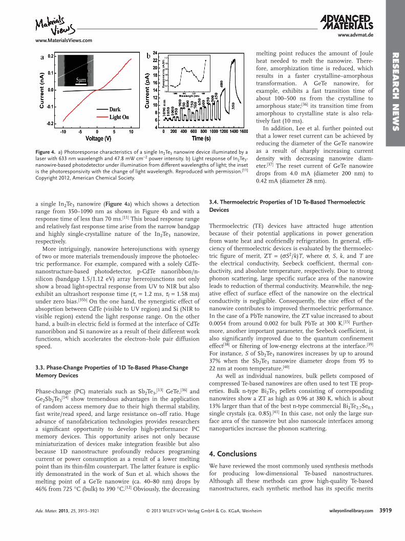
Figure 4 . a) Photoresponse characteristics of a single In 2 Te 3 nanowire device illuminated by a laser with 633 nm wavelength and 47.8 mW cm − 2 power intensity. b) Light response of In 2 Te 3 -nanowire-based photodetector under illumination from different wavelengths of light; the inset is the photoresponsivity with the change of light wavelength. Reproduced with permission. [ 11 ] Copyright 2012, American Chemical Society.
a single In 2 Te 3 nanowire ( Figure 4 a) which shows a detection range from 350–1090 nm as shown in Figure 4 b and with a response time of less than 70 ms. [ 11 ] This broad response range and relatively fast response time arise from the narrow bandgap and highly single-crystalline nature of the In 2 Te 3 nanowire, respectively.
More intriguingly, nanowire heterojunctions with synergy of two or more materials tremendously improve the photoelec-tric performance. For example, compared with a solely CdTe-nanostructure-based photodetector, p-CdTe nanoribbon/n-silicon (bandgap 1.5/1.12 eV) array hererojunctions not only show a broad light-spectral response from UV to NIR but also exhibit an ultrashort response time ( τ r = 1.2 ms, τ f = 1.58 ms) under zero bias. [ 35b ] On the one hand, the synergistic effect of absoprtion between CdTe (visible to UV region) and Si (NIR to visible region) extend the light response range. On the other hand, a built-in electric fi eld is formed at the interface of CdTe nanoribbon and Si nanowire as a result of their different work functions, which accelerates the electron–hole pair diffusion speed.
3.3. Phase-Change Properties of 1D Te-Based Phase-Change Memory Devices
Phase-change (PC) materials such as Sb 2 Te 3 , [ 13 ] GeTe, [ 36 ] and Ge 2 Sb 2 Te 5 [ 14 ] show tremendous advantages in the application of random access memory due to their high thermal stability, fast write/read speed, and large resistance on–off ratio. Huge advance of nanofabrication technologies provides researchers a signifi cant opportunity to develop high-performance PC memory devices. This opportunity arises not only because miniaturization of devices make integration feasible but also because 1D nanostructure profoundly reduces programing current or power consumption as a result of a lower melting point than its thin-fi lm counterpart. The latter feature is explic-itly demonstrated in the work of Sun et al. which shows the melting point of a GeTe nanowire (ca. 40–80 nm) drops by 46% from 725 ° C (bulk) to 390 ° C. [ 12 ] Obviously, the decreasing
© 2013 WILEY-VCH Verlag GmbH & Co. KGaA, WeinhAdv. Mater. 2013, 25, 3915–3921
melting point reduces the amount of Joule heat needed to melt the nanowire. There-fore, amorphization time is reduced, which results in a faster crystalline–amorphous transformation. A GeTe nanowire, for example, exhibits a fast transition time of about 100–500 ns from the crystalline to amorphous state; [ 36 ] its transition time from amorphous to crystalline state is also rela-tively fast (10 ms).
In addition, Lee et al. further pointed out that a lower reset current can be achieved by reducing the diameter of the GeTe nanowire as a result of sharply increasing current density with decreasing nanowire diam-eter. [ 37 ] The reset current of GeTe nanowire drops from 4.0 mA (diameter 200 nm) to 0.42 mA (diameter 28 nm).
3.4. Thermoelectric Properties of 1D Te-Based Thermoelectric Devices
Thermoelectric (TE) devices have attracted huge attention because of their potential applications in power generation from waste heat and ecofriendly refrigeration. In general, effi -ciency of thermoelectric devices is evaluated by the thermoelec-tric fi gure of merit, ZT = ( σ S 2 / k ) T , where σ , S , k , and T are the electrical conductivity, Seebeck coeffi cient, thermal con-ductivity, and absolute temperature, respectively. Due to strong phonon scattering, large specifi c surface area of the nanowire leads to reduction of thermal conductivity. Meanwhile, the neg-ative effect of surface effect of the nanowire on the electrical conductivity is negligible. Consequently, the size effect of the nanowire contributes to improved thermoelectric performance. In the case of a PbTe nanowire, the ZT value increased to about 0.0054 from around 0.002 for bulk PbTe at 300 K. [ 15 ] Further-more, another important parameter, the Seebeck coeffi cient, is also signifi cantly improved due to the quantum confi nement effect [ 38 ] or fi ltering of low-energy electrons at the interface. [ 39 ] For instance, S of Sb 2 Te 3 nanowires increases by up to around 37% when the Sb 2 Te 3 nanowire diameter drops from 95 to 22 nm at room temperature. [ 40 ]
As well as individual nanowires, bulk pellets composed of compressed Te-based nanowires are often used to test TE prop-erties. Bulk n-type Bi 2 Te 3 pellets consisting of corresponding nanowires show a ZT as high as 0.96 at 380 K, which is about 13% larger than that of the best n-type commercial Bi 2 Te 2.7 Se 0.3 single crystals (ca. 0.85). [ 41 ] In this case, not only the large sur-face area of the nanowire but also nanoscale interfaces among nanoparticles increase the phonon scattering.
4. Conclusions
We have reviewed the most commonly used synthesis methods for producing low-dimensional Te-based nanostructures. Although all these methods can grow high-quality Te-based nanostructures, each synthetic method has its specifi c merits
3919wileyonlinelibrary.comeim
3920
www.advmat.dewww.MaterialsViews.com
RES
EARCH N
EWS
and disadvantages. The vapor–solid deposition method exhibitspronounced superiority in synthesizing highly pure few-layer layered-structure 2D Te-based nanostructures, but its yield is moderate and quality is very sensitive to the growth tempera-ture. Vapor–liquid–solid deposition can effectively defi ne the growth direction and diameter of nanowire by using an Au cat-alyst, while the Au catalyst also causes contamination of the Te-based nanowire. In contrast to vapor-phase deposition, the yield of solvothermal/hydrothermal methods is much larger. Never-theless these methods involve a complicated chemical reaction process which is time-consuming and detrimental to the envi-ronment. In brief, when choosing a suitable growth technology, comprehensive consideration should be made of yield, quality, purity, cost, controllability, time consumption, etc.
Successful synthesis of high-quality single-crystalline low-dimensional Te-based nanostructures provides an important opportunity to realize their practical applications in future information and energy technologies. Compared with the bulk counterpart, a low-dimensional Te-based topological insulator profoundly strengthens surface-state effects and thus paves the way for its applications in dissipationless spintronic devices and quantum computation. Also, nano-optoelectronic devices confi gured from low-dimensional Te-based small bandgap semiconductors, which are highly single crystalline, not only show high photoelectric-detection quantum effi ciency but also have potential advantages in fabricating the active element of an integrated circuit. Meanwhile, 1D Te-based phase-change memory device already have this kind of compatibility with an integrated circuit. Beyond that, in comparison with thin-fi lm phase-change memory devices, 1D Te-based phase-change memory devices reduce the programming current due to the reduction of dimensions. Combined with their intrinsic fea-tures of fast writing/reading and improved endurance, 1D Te-based resistive phase-change memory devices are one of the promising alternatives for substituting conventional tran-sistor-based nonvolatile memories. In addition, nanoscale thermoelectronic devices seem to be ideal for the application of salvaging wasted heat energy from fossil-fuel combustion engines, which could result in signifi cant reduction of green-house gases.
However, it is worth noting that the way to commercial appli-cations of Te-based nanoscale electronic and optoelectronic devices must still face main challenges from: 1) chemical/mechanical/physical instability of low-dimensional Te-based nanostructures; 2) diffi culties in fabricating an integrated circuit and problems caused by integration such as current leakage. Therefore, researchers need to make more efforts to overcome these weaknesses and thus realize industrial applica-tions in the future.
Acknowledgements This study was supported by the 973 Program of the Ministry of Science and Technology of China (no. 2012CB934103) and the 100-Talents Program of the Chinese Academy of Sciences (no. Y1172911ZX).
Received: March 12, 2013 Revised: April 9, 2013
Published online: May 27, 2013
wileyonlinelibrary.com © 2013 WILEY-VCH Verlag G
[ 1 ] a) Z. L. Wang , J. Song , Science 2006 , 312 , 242 ; b) Z. L. Wang , Adv. Mater. 2012 , 34 , 4629 .
[ 2 ] S. Myung , A. Solanki , C. Kim , J. Park , K. S. Kim , K. Lee , Adv. Mater. 2011 , 23 , 2221 .
[ 3 ] J. Tang , Z. Huo , S. Brittman , H. Gao , P. Yang , Nat. Nanotechnol. 2011 , 6 , 568 .
[ 4 ] X. Fang , S. Xiong , T. Zhai , Y. Bando , M. Liao , U. K. Gautam , Y. Koide , X. Zhang , Y. Qian , D. Golberg , Adv. Mater. 2009 , 21 , 5016 .
[ 5 ] a) Y. Chen , J. G. Analytis , J. Chu , Z. Liu , S. Mo , X. Qi , H. Zhang , D. Lu , X. Dai , Z. Fang , S. Zhang , I. R. Fisher , Z. Hussain , Z. Shen , Science 2009 , 325 , 178 ; b) Y. Li , G. Wang , X. Zhu , M. Liu , C. Ye , X. Chen , Y. Wang , K. He , L. Wang , X. Ma , H. Zhang , X. Dai , Z. Fang , X. Xie , Y. Liu , X. Qi , J. Jia , S. Zhang , Q. Xue , Adv. Mater. 2010 , 22 , 4002 ; c) G. Wang , X. Zhu , Y. Sun , Y. Li , T. Zhang , Jing Wen , X. Chen , K. He , L. Wang , X. Ma , J. Jia , S. B. Zhang , Q. Xue , Adv. Mater. 2011 , 23 , 2929 ; d) J. H. Chang , T. Takai , B. H. Koo , J. S. Song , T. Handa , T. Yao , Appl. Phys. Lett. 2001 , 79 , 785 ; e) J. Britta , C. Ferekides , Appl. Phys. Lett. 1993 , 62 , 2851 ; f) T. D. Golding , P. R. Boyd , M. Martinka , P. M. Amlrtharaj , J. H. Dinan , S. B. Qadri , D. R. T. Zahn , C. R. Whitehouse , J. Appl. Phys. 1989 , 65 , 1936 ; g) S. K. Bahl , K. L. Chopra , J. Appl. Phys. 1970 , 41 , 2196 ; h) A. Majumdar , Sci-ence 2004 , 303 , 777 ; i) T. C. Harman , P. J. Taylor , M. P. Walsh , B. E. LaForge , Science 2002 , 297 , 2229 .
[ 6 ] S. Lee , J. In , Y. Yoo , Y. Jo , Y. C. Park , H. Kim , H. C. Koo , J. Kim , B. Kim , K. L. Wang , Nano Lett. 2012 , 12 , 4194 .
[ 7 ] F. Xiu , L. He , Y. Wang , L. Cheng , L. Chang , M. Lang , G. Huang , X. Kou , Y. Zhou , X. Jiang , Z. Chen , J. Zou , A. Shailos , K. L. Wang , Nat. Nanotechnol. 2011 , 6 , 205 .
[ 8 ] G. Hao , X. Qi , G. Wang , X. Peng , S. Chang , X. Wei , J. Zhong , RSC Adv. 2012 , 2 , 10694 .
[ 9 ] Z. Li , J. Salfi , C. D. Souza , P. Sun , S. V. Nair , H. E. Ruda , Appl. Phys. Lett. 2010 , 97 , 063510 .
[ 10 ] X. Xie , S. Kwok , Z. Lu , Y. Liu , Y. Cao , L. Luo , J. Zapien , I. Bello , C. Lee , S. Lee , W. Zhang , Nanoscale 2012 , 4 , 2914 .
[ 11 ] Z. Wang , M. Safdar , C. Jiang , J. He , Nano Lett. 2012 , 12 , 4715 . [ 12 ] X. Sun , B. Yu , G. Ng , M. Meyyappan , J. Phys. Chem. C 2007 , 111 ,
2421 . [ 13 ] J. S. Lee , S. Brittman , D. Yu , H. Park , J. Am. Chem. Soc. 2008 , 130 ,
6252 . [ 14 ] Y. Jung , S. Lee , D. Ko , R. Agarwal , J. Am. Chem. Soc. 2006 , 128 ,
14026 . [ 15 ] S. H. Lee , W. Shim , S. Y. Jang , J. W. Roh , P. Kim , J. Park , W. Lee ,
Nanotechnol. 2011 , 22 , 295707 . [ 16 ] H. Li , J. Cao , W. Zheng , Y. Chen , D. Wu , W. Dang , K. Wang , H. Peng ,
Z. Liu , J. Am. Chem. Soc. 2012 , 134 , 6132 . [ 17 ] G. Tai , B. Zhou , W. Guo , J. Phys. Chem. C 2008 , 112 , 11314 . [ 18 ] K. Wang , H. Liang , W. Yao , S. Yu , J. Mater. Chem. 2011 , 21 , 15057 . [ 19 ] C. Chen , Y. Chen , S. Lin , J. C. Ho , P. Lee , C. Chen , S. R. Harutyunyan ,
J. Phys. Chem. C 2010 , 114 , 3385 . [ 20 ] S. Lee , J. In , Y. Yoo , Y. Jo , Y. C. Park , H. J. Kim , H. C. Koo , J. Kim ,
B. Kim , K. L. Wang , Nano Lett. 2012 , 12 , 4194 . [ 21 ] D. Kong , W. Dang , J. J. Cha , H. Li , S. Meister , H. Peng , Z. Liu , Y. Cui ,
Nano Lett. 2010 , 10 , 2245 . [ 22 ] M. Safdar , Z. Wang , M. Mirza , C. Jiang , J. He , J. Mater. Chem. 2012 ,
22 , 19228 . [ 23 ] K. Wang , H. Liang , W. Yao , S. Yu , J. Mater. Chem. 2011 , 21 , 15057 . [ 24 ] G. Zhang , H. Fang , H. Yang , L. A. Jauregui , Y. P. Chen , Y. Wu , Nano
Lett. 2012 , 12 , 3627 . [ 25 ] M. Safdar , Z. Wang , M. Mirza , F. K. Butt , Y. Wang , L. Sun , J. He ,
J. Mater. Chem. A 2013 , 1 , 1427 . [ 26 ] a) J. Zhang , S. Jin , H. C. Fry , S. Peng , E. Shevchenko , G. P. Wiederrecht ,
T. Rajh , J. Am. Chem. Soc. 2011 , 133 , 15324 ; b) J. Zhang , K. Sun , A. Kumbhar , J. Fang , J. Phys. Chem. C 2008 , 112 , 5454 .
[ 27 ] a) D. Qu , Y. S. Hor , J. Xiong , R. J. Cava , N. P. Ong , Science 2010 , 329 , 821 ; b) M. Z. Hasan , C. L. Kane , Rev. Mod. Phys. 2010 , 82 , 3045 .
mbH & Co. KGaA, Weinheim Adv. Mater. 2013, 25, 3915–3921

www.advmat.de
RES
EARCH N
EWS
www.MaterialsViews.com
[ 28 ] Y. Wang , F. Xiu , L. Cheng , L. He , M. Lang , J. Tang , X. Kou , X. Yu , X. Jiang , Z. Chen , J. Zou , K. L. Wang , Nano Lett. 2012 , 12 , 1170 .
[ 29 ] D. Kong , W. Dang , J. J. Cha , H. Li , S. Meister , H. Peng , Z. Liu , Y. Cui , Nano Lett. 2010 , 10 , 2245 .
[ 30 ] Y. S. Hor , A. Richardella , P. Roushan , Y. Xia , J. G. Checkelsky , A. Yazdani , M. Z. Hasan , N. P. Ong , R. J. Cava , Phy. Rev. B 2009 , 79 , 195208 .
[ 31 ] D. Kong , Y. Chen , J. J. Cha , Q. Zhang , J. G. Analytis , K. Lai , Z. Liu , S. S. Hong , K. J. Koski , S. Mo , Z. Hussain , I. R. Fisher , Z. Shen , Y. Cui , Nat. Nanotechnol. 2011 , 6 , 705 .
[ 32 ] Z. Ren , A. A. Taskin , S. Sasaki , K. Segawa , Y. Ando , Phys. Rev. B 2010 , 82 , 241306 .
[ 33 ] J. J. Cha , D. Kong , S. Hong , J. G. Analytis , K. Lai , Y. Cui , Nano Lett. 2012 , 12 , 1107 .
[ 34 ] a) Z. Li , J. Salfi , C. D. Souza , P. Sun , S. V. Nair , H. E. Ruda , Appl. Phys. Lett. 2010 , 97 , 063510 ; b) Y. L. Cao , Z. T. Liu , L. M. Chen , Y. B. Tang , L. B. Luo , J. S. Jie , W. J. Zhang , S. T. Lee , C. S. Lee , Opt. Express 2011 , 19 , 6100 .
© 2013 WILEY-VCH Verlag GAdv. Mater. 2013, 25, 3915–3921
[ 35 ] a) Y. Ye , L. Dai , T. Sun , L. P. You , R. Zhu , J. Y. Gao , R. M. Peng , D. P. Yu , G. G. Qin , J. Appl. Phys. 2010 , 108 , 044301 ; b) C. Xie , L. Luo , L Zeng , L. Zhu , J. Chen , B. Nie , J. Hu , Q. Li , C. Wu , L. Wang , J. Jie , CrystEngComm 2012 , 14 , 7222 ; c) X. Xie , S. Kwok , Z. Lu , Y. Liu , Y. Cao , L. Luo , J. A. Zapien , I. Bello , C. Lee , S. Lee , W. Zhang , Nanoscale 2012 , 4 , 2914 .
[ 36 ] D. Yu , J. Wu , Q. Gu , H. Park , J. Am. Chem. Soc. 2006 , 128 , 8148 .
[ 37 ] S. Lee , D. Ko , Y. Jung , R. Agarwal , Appl. Phys. Lett. 2006 , 89 , 223116 .
[ 38 ] T. E. Humphrey , H. Linke , Phys. Rev. Lett. 2005 , 94 , 096601 . [ 39 ] J. Martin , L. Wang , L. Chen , G. S. Nolas , Phys. Rev. B 2009 , 79 ,
115311 . [ 40 ] Y. M. Zuev , J. S. Lee , C. Galloy , H. Park , P. Kim , Nano Lett. 2010 , 10 ,
3037 . [ 41 ] J. S. Son , M. K. Choi , M. Han , K. Park , J. Kim , S. J. Lim , M. Oh ,
Y. Kuk , C. Park , S. Kim , T. Hyeon , Nano Lett. 2012 , 12 , 640 .
3921wileyonlinelibrary.commbH & Co. KGaA, Weinheim