Low Cost Processing for 3D TSV Applicationkmeps.or.kr/UploadData/Editor/BBS1/201501/4A460536E... ·...
23
Slide 1 TRUST: Cavity and Cube, Confidential, 2014 Low Cost Processing for 3D TSV Application 2014. 8 Gu-Sung Kim, Ph.D, Th.M. KNU. Korea/EPWorks, Korea
Transcript of Low Cost Processing for 3D TSV Applicationkmeps.or.kr/UploadData/Editor/BBS1/201501/4A460536E... ·...

Slide 1
TRUST: Cavity and Cube, Confidential, 2014
Low Cost Processing for 3D TSV Application
2014. 8
Gu-Sung Kim, Ph.D, Th.M.
KNU. Korea/ EPWorks, Korea
Founded by TSV Engineers at 2006 World first 12inch TSV Infrastructure for interposer Production and Proto-Type Service for interposer and TSV products Materials and Process Development for Low Cost EPW designed Process and Equipment Development for Mass
Production
Company Position
GS Kim, EPWorks/KNU, 2014

• Semiconductor transformed into 3D IC
• Development of semiconductor needed for high-speed high-performance
- Wide I/O2 >25.6GB/s - HBM (High Bandwidth Memory)
introduced(2013/2014) >1Tbits/s • Emergence of semiconductors that employ
Through Silicon VIA (TSV) technology for 3D IC
- Only technology that provides data pathway between processor and memory
- Only technology that maximizes bandwidth - Technology that reduces power consumption
and maximizes power distribution and heat dissipation
• 3D TSV semiconductor will be the core component in future mobile devices for reducing power consumption and form factor
• Network and cloud computing equipment will utilize 2.5D TSV semiconductor for high capacity and high bandwidth
Tomorrow’s Semiconductor and 3D IC
Currently deployed logic IC + memory IC TSV chip : Uses TSV Interposer
Semiconductor Change
GS Kim, EPWorks/KNU, 2014

EPWorks Interposer
EPWorks’ Unique Interposer Solutions
Process : TSV process, Dual-sided RDL (rewired) technology, u-Bump and MEMs combined technology
Equipment : TSV core equipment developed and successfully deployed.
Materials : Developed silicon that optimizes performance/cost of TSV to be deployed in 2013 H2
R&D : Completed 9 National R&D projects related to TSV and currently pursuing joint
development with universities, research centers and private enterprises within/out Korea
( High AR PVD - Developed with part maker)
( W2W Bonder - Developed with Vendor)
( 12inch DRIE - Developed with Vendor)
( 12inch Double Side Aligner - Developed with Vendor)
GS Kim, EPWorks/KNU, 2014

Feature . 3D Enabling with 100% Yield Module
. TSV (Thru-silicon-Via) Connection
. Re-Distribution Interposer
. Wafer and Panel Type
Structure . Wafer to Wafer (Same Die)
. Chip to Wafer (Different Die)
. Cavity and Cube for High Frequency
. Unique Module Recover Pattern
. Pad-on-Back Connection for CIS
g-STACK® g-INTERPOSER®
Interposer for SOC Application
Package Solution for 3D Stacked IC and FC-BGA Package High Reliability because of using the Silicon Substrate Interposer Chip Design and Manufacturing Experience Low Cost Solution Design Rule for TSV Via Size (10, 20, 50, 100um) Process and Equipment Development for Mass Production Level
Memory #2
Processor “T”
Memory #1
EPworks Std. Interposer
(10-20um Via x 70-100um Depth)
GS Kim, EPWorks/KNU, 2014

EPW Grade
Leti
KSIA/IMEC
Via size
Via pitch
Wafer thickness
On-Chip Interconnect level
0 level packaging
Global level
Intermediate level
Local interconnect Floating Cell
• Standard Si • Prefer Via Last • 2.5D Interposer • Multi-source possible • Post-foundry process • C2C or C2W stacking • Mainly parallel process • Cost driven
• BEOL level process • Thin/stack – WL process • Prefer Via Last or Via Middle • C2W or W2W stacking • 3D Interposer • Cost and TPH – Trade -off • Mainly parallel process
• FEOL level process • Prefer Via First or Cell Stack • Requires use of SOI wafers • W2W stacking • Extreme W2W alignment
accuracy • 3D Interposer • Yield issues
80 um
100 um
50 um 2 um
15 um
7 um 5 um
4 um
100 nm
1 um 200 nm
Active layer only - SOI
500 nm 25 um
40 um
50 um 20 um 35 um
10 um
15 um
10 um
20 um
30 um
3D-WLP TSV 3D-Stacked ICs TSV 3D-IC Sub-μ TSV
Wafer level
3D Interconnection Interposer Classification
Smart Interposer HD Interposer
W3 W2 W1 W4
GS Kim, EPWorks/KNU, 2014

Interposer Type Organic Si/Glass Silicon
IC-to-Package I/O Pad Pitch
50-250μm 20-100μm <40μm
Line Dimension (Typ.) > 15μm > 5μm > 0.5
Trends Embedded Passive Flex Based
LDI Process for 10μm Fab Infrastructure
Substrate Size >12inch Panel Process
Thermal Performance New Materials
Cu Damascene Via First
W2W Bonding
Commercial Approach HD Substrate Embedded Substrate Integrated Passive Substrate
- Cost of raw core Low
Si : Recycled Wafer Glass : Via Formed by
MFG.
Si : Graded Wafer
- Process cost cents/mm² < 0.5 0.5 ~ 2 > 3
Company >12inch based
8inch based
Ibiden, Semco
EPW
LETI, Silex
TSMC, UMC, GF
EPW (2015)
Design for Reducing # of Masks SOC Design Customer Requirement OSATs Requirement
Cost Solution
3 types Interposer
Interposer Materials Trend
GS Kim, EPWorks/KNU, 2014

Wafer
Via Filing
Via Formation
Metal Bumping
Align/Bonding
Soldering
Sawing
Thinning
Tested Wafer - Standard EDS
- No Test
Wafer-level Processing +
Wafer Stack
Wafer Level Test/BI - Normal - @ Speed (Memory)
3D Chip Test - Repair
- Module Level - Chip/Package Level
Material Process Chemical Process Lithography Electrical/Mechanical Structure Components
Interposer Silicon, Glass
3D IC Package, Module
Interposer Process Interposer Materials Trend
GS Kim, EPWorks/KNU, 2014

Why EPWorks Solution!!
Convergence IT System Solution in Hybrid – Active and Passive Component
The First g-Stack Solution – Powerful Patent Map
Interposer Line-Up – 8inch and 12inch Infrastructure
TSV Experts
TSV dedicated Equipment R&D – Successive Process Recipe
Low Cost TSV Process R&D
Abundant Customer Specification
10um ~ 100um TSV Interposer/ 2um ~ 20um L/S Interconnection
Wafer to Wafer Stack Process
3D IC Biz solution – up to 12inch Interposer, Via Last TSV, g-Interposer
TSV Equipment (Deep RIE, PVD, Flux Reflow etc.) - 1/3 of Investment in
Process
Low Cost Interposer – Cost Effective TSV Line, Si Wafer Manufacturing
World Leading Technology
GS Kim, EPWorks/KNU, 2014

Stacking Process Optimization Pre-Pattern Underfill M-Fuse Process
g-STACK 3D Structure
EPWorks Patented Structure
n Stacks
Wafer Bonding - Adhesive (< 10µm) - Metal (< 350oC)
Optimize Bonding Process Wafer Warpage
Stress Simulation after 3D Integration Failure Analysis
Low Temp Cu Bonding Pre-Treatment Process
High Reliability Bonding Structure Device Modeling
Simulation tool Development
TSV Via Size: < 30µm
50~80 µm
g-Stack® Structure
GS Kim, EPWorks/KNU, 2014

EPWorks Interposer
u-bumps/ Cu Post/ Si Post > 7um Diameter
Bumps or Copper pillars
10um Via x 100um Depth Double Via
Interconnection 5um L/S 3 Layer ILD
Interposer
T S V
15um Via x 70um THK
Cu Fill Interposer
BVR (Backside Via Reveal) 1M Via/wafer, CMP and Si Dry Etch
TSV Formation/Isolation > 5um ~ 100um
GS Kim, EPWorks/KNU, 2014
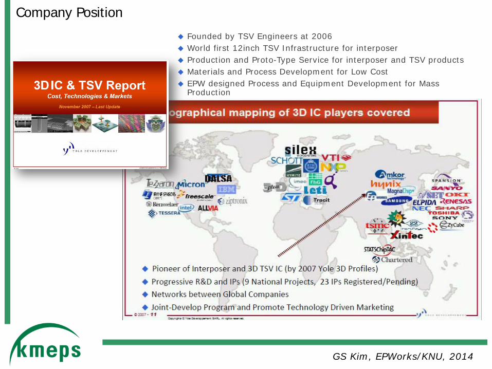
Wafer Biz. / TSV Solution Memory
Wafer Biz Logic
Wafer Biz
WLP/Bump Product
TSV is Right Solution : 3D IC & SIP Solution : Function / Quality / Price & Cost - Right Time Market
InterposerWafer Biz
TSV/3D Applications
GS Kim, EPWorks/KNU, 2014
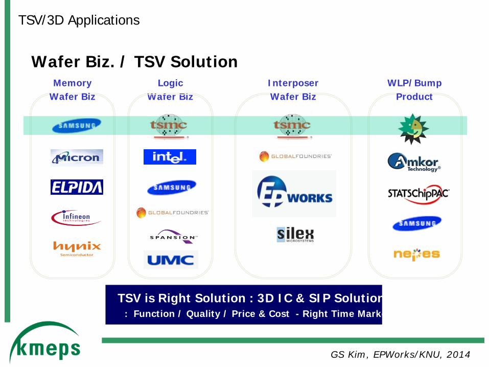
Business Application
2011 2012 2013 2014 2015
Logic Dram Dram
CIS TSV WLP
AP
3D CIS CIS
Interposer DSP
LED- MEMS Interposer
BSI TSV-WLP CIS
Interposer
Logic - SIP
MEMS
CIS
Memory NAND 3D Si-IP
Interposer Interposer
2.5D Interposer
3D Interposer
AP - IPD
MEMS WLP LED
GS Kim, EPWorks/KNU, 2014

HB-LED Si Carrier
• Multi-LED dies for Sub-Mount • LED Wafer Level Package with Hermetic TSI • One body Si Carrier from Sub-Mount to Substrate • Thermal Conductivity : Similar with Al • CTE Match with LED Die : Similar with AlN • Cost of 12inch EPworks Carrier: Similar with Al2O3
• Embedded EPworks IPD to 12inch wafer • Wafer to Wafer Bond Structure
SiC
GaN AlN
Si
Cu
Al
PCB
SiO2 Alumina
0
5
10
15
20
25
0.1 1 10 100 1000
Thermal conductivity w/m-k
Coef
ficie
nt o
f The
rmal
Exp
ansio
n
Ready for Mass Production
• 100um to 500um Substrate Thickness • Low Cost and High Batch Solution • Deep RIE and/or KOH/TMAH Wet Etch alternatively • Oxide or Nitride Isolation Layer • Side/Full Via Metallization with Cu or Else. • Metal Finish for Ultrasonic Bonding or Flip Chip Process
LED Interposer
Interposer for LED Application
GS Kim, EPWorks/KNU, 2014

Wet Etch Masking
Electro Plating
PR Patterning
Via Isolation
Mask Etching
Via Etching
Seed Deposition
Simple Process
EPWorks 12inch LED Interposer (TSV with 20um Cu Line Both Side)
TSV Pitch
Solder bump (Optional)
Wet Etch Via 300um ■SQ 20um ■SQ
(Optional) DRIE Via 50um ● (A/R 8:1)
Core Technology
GS Kim, EPWorks/KNU, 2014

• Main applications: - logic, memory, analog & mixed signal
• Available on 4 to 12inch wafer • TSV and Multilayer Redistributed Cu with Passivation • Up to 3 layer with Cu/PI or Cu/SiO2 • Two types of Through Via architectures • TEG Interposer for Low Cost Solution • 50um to 400um Si Thickness with High AR Via Filled • Typical Via Diameter is 10µm with 100um thickness • Cu, Cu/Ni, Au, Sn or Sn-Ag Metal Finished including UBM • CMP Process Both Side and Cavity Available
• Main applications: - Opto-MEMS and RF Application
• Available on 4 to 12inch Glass Wafer • Etch and/or Blasting Alternatively • 45um to 500um Glass Thickness • Typical Via Diameter is 50um with 300um pitch • Metal on PSPI/Polymer Pattern • U-Bump on Glass
Glass Interposer
General Feature
Memory #2
Processor “T”
Memory #1
Si Interposer
silicon
Seed + Via
Mor
e th
an
100µ
m
insulation
Interposer for 2.5/3D IC
GS Kim, EPWorks/KNU, 2014

CIS BSI TSV Process Patented Protected
•Main application: CMOS Image Sensor (BSI) • Back-Side Illuminated CMOS-Image Sensor • TSV Interposer Package • Unique g-Stack Interconnection with Full Patented • BSI Chip Thickness < 15um – Wafer Thinning Only • >30um Std. Via-First Process • Standard Side-Fill • Wafer-to-Wafer Bonding
Interposer for BSI CIS
BSI FSI
Si / Glass Interposer (2007 ~ 2010)
GS Kim, EPWorks/KNU, 2014
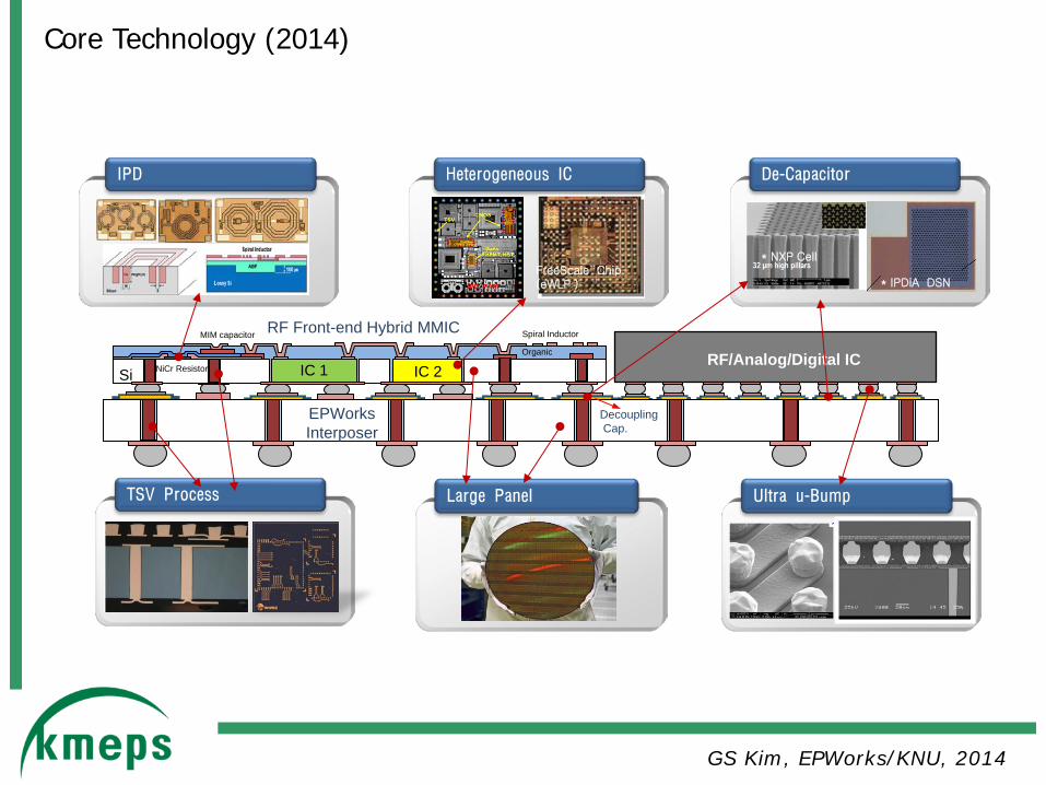
IPD
Heterogeneous IC
De-Capacitor
TSV Process
Ultra u-Bump
Large Panel
FreeScale Chip (eWLP ) * IPDiA DSN
* NXP Cell
Spiral Inductor
Organic
` NiCr Resistor
MIM capacitor
IC 1 Si IC 2 RF/Analog/Digital IC
RF Front-end Hybrid MMIC
EPWorks Interposer
Decoupling Cap.
Core Technology (2014)
GS Kim, EPWorks/KNU, 2014
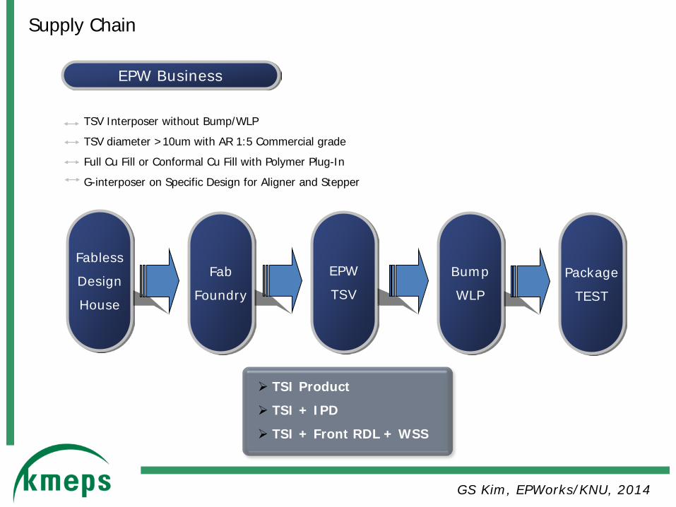
EPW Business
Fabless
Design
House
Package
TEST
Fab
Foundry
EPW
TSV
Bump
WLP
TSV Interposer without Bump/WLP TSV diameter >10um with AR 1:5 Commercial grade Full Cu Fill or Conformal Cu Fill with Polymer Plug-In G-interposer on Specific Design for Aligner and Stepper
Supply Chain
TSI Product TSI + IPD TSI + Front RDL + WSS
GS Kim, EPWorks/KNU, 2014

Cost Solution
Interposer Mass Production
Cost, TPH, Yield
Interposer Structure
Minimized Component
Simple Process
Materials Si Size issues
Wafer / Panel
High TPH Equipment
Low cost Process
<$700 ~ $1500 ~ $3000 < per 12inch Standard Wafer Process
Low Cost Solution
GS Kim, EPWorks/KNU, 2014

Sludge
Floatation
Agitation
Dry
Casting
Substrate Tooling
Interposer
Chemical Clean
Back Lap/Grind - Standard In-Line Chemical Solution
Al Separation Impurity Control Process Spec.
3N Powder
)
SPS (1275℃-5min)
Hot Press (1,300℃-2h)
g-Interposer® Substrate
GS Kim, EPWorks/KNU, 2014

Si Refining Technology Si Interposer and Growing
Interposer Substrate - Ingot Type ( 8 ~ 12inch CZ ) - Casting (>6inch SQ) - >100Ohm Intrinsic HRS
Back Grinding Sludge - Single Crystal Si + Al contained Impurity - Physical + Chemical Refining
g-Interposer® Substrate
GS Kim, EPWorks/KNU, 2014

Copyright © 2014 by EPWorks & Kangnam University
All rights reserved.
The materials in this presentation may not be reproduced, in whole or in part, in any manner or in any form or otherwise without the written permission of EPWorks.
Slide 23
TRUST: Cavity and Cube, Confidential, 2014