Low-Cost Digital Ultrasound Beamformer Design using … · i Low-Cost Digital Ultrasound Beamformer...
165
Cairo University Low-Cost Digital Ultrasound Beamformer Design using Field Programmable Gate Arrays By Basem Ahmed Hassan Systems and biomedical Engineering Department Faculty of Engineering, Cairo University A thesis submitted to the Faculty of Engineering, Cairo University In Partial Fulfillment of the Requirements for the degree of Master of Science In SYSTEMS AND BIOMEDICAL ENGINEERING FACULTY OF ENGINEERING, CAIRO UNIVERSITY GIZA, EGYPT 2012
Transcript of Low-Cost Digital Ultrasound Beamformer Design using … · i Low-Cost Digital Ultrasound Beamformer...

Cairo University
Low-Cost Digital Ultrasound Beamformer Design using Field
Programmable Gate Arrays
By
Basem Ahmed Hassan
Systems and biomedical Engineering Department
Faculty of Engineering, Cairo University
A thesis submitted to the
Faculty of Engineering, Cairo University
In Partial Fulfillment of the
Requirements for the degree of
Master of Science
In
SYSTEMS AND BIOMEDICAL ENGINEERING
FACULTY OF ENGINEERING, CAIRO UNIVERSITY
GIZA, EGYPT
2012

i
Low-Cost Digital Ultrasound Beamformer Design using Field
Programmable Gate Arrays
By
Basem Ahmed Hassan
Systems and biomedical Engineering Department
Faculty of Engineering, Cairo University
A thesis submitted to the
Faculty of Engineering, Cairo University
In Partial Fulfillment of the
Requirements for the degree of
Master of Science
In
SYSTEMS AND BIOMEDICAL ENGINEERING
Under the supervision of
Prof. Dr. Yasser Mostafa Kadah
Systems and biomedical Engineering Department
Faculty of Engineering, Cairo University
FACULTY OF ENGINEERING, CAIRO UNIVERSITY
GIZA, EGYPT
OCTOBER 2012

ii
Low-Cost Digital Ultrasound Beamformer Design using Field
Programmable Gate Arrays
By
Basem Ahmed Hassan
Systems and biomedical Engineering Department
Faculty of Engineering, Cairo University
A thesis submitted to the
Faculty of Engineering, Cairo University
In Partial Fulfillment of the
Requirements for the degree of
Master of Science
In
SYSTEMS AND BIOMEDICAL ENGINEERING
Approved by the Examining Committee:
Prof. Dr. Yasser Mostafa Kadah, Thesis Main Advisor
Prof. Dr. Magdy Fekry, Member
Prof. Dr. Mohammed Ibrahim El Adway, Member
FACULTY OF ENGINEERING, CAIRO UNIVERSITY
GIZA, EGYPT
OCTOBER 2012

Abstract
iii
Abstract
Real-time ultrasonic imaging systems have been available for more than sixty
years and are becoming an important tool in the practice of modem medicine. During this
time much has occurred to the basic architecture and functions of these clinical systems
and their beamformers, which are, in many ways, the most important components of
these systems. Throughout most of the 30 years of real time imaging, analog
beamformers have been the mainstay of al1 ultrasonic instruments. But at the present
time the industry is undergoing a major shift toward digital beamformation with the
introduction of several commercial systems. Our thesis describes a novel extendable
Beamforming architecture design in both of the system-level Hardware and Firmware
design level. In the Hardware design, we were targeting the compactable application as
well as the extendable applications where the power, level of integration and the feasible
of the replication are critical. The three main components that have the greatest influence
on the hardware design and system performance of the signal-processing board are the
Analog to Digital Converters (ADCs), the Beamformer transmitter and the FPGA. We
could utilize the TI AFE5801 as the analog front end of the beamforming by using its
eight ADC in one IC as well as using the LM96570 the ultrasound transmitter as an
integrated solution for sending a Full control ultrasound signal over selecting beam
directions for eight channels. This lead to a dramatically decrease of the size, cost and the
power making from the proposed design an ideal solution for the low-cost ultrasound
imaging devices. On the other hand due to the firmware design we utilized the next-
generation high level synthesize tool VIVADO HLS tool the new IP and system-centric
design environment to accelerate the design productivity with up to 4 X productivity
gain. Using this tool lead us to achieve the optimum degree of FPGA parallelism. The
technical challenges in digital beamformation will be reviewed, we will have a look at
our digital beamformers simulation and its performance compared in terms of beam
width, side lobe levels and signal-to-noise ratio. Finally, the future work of our digital
beamformer in the context of advances features and the missing will be discussed.

ACKNOWLEDGMENTS
iv
ACKNOWLEDGMENTS
Firstly I would like to thank God for giving me health and patience in completing
this thesis. Over the two years that I spent on research, for my thesis, many people have
helped me to reach my objective of completing it. I take this opportunity to thank them
all. The time spent on my graduate work has not only been, learning exercise
academically but also an enriching one personally. First of al1 I would like to thank my
thesis advisor, Dr. Yasser Mostafa Kadah for his remarkable patience. I would like to
thank my kind and humble friends; I would like to mention how much I appreciate every
professor at Cairo University that I have had the pleasure to know. The
Noacknowledgement would be complete without mentioning the support, acceptance,
and love of my family, my Father, my Mother, My Brothers, Sisters, my wife and my
Child.

Table of Contents
v
Table of Contents
ACKNOWLEDGMENT ....................................................................................... IV
TABLE OF CONTENETS ...................................................................................... V
LIST OF TABLES ................................................................................................ IX
LIST OF FIGURES .............................................................................................. XV
NOMENCLATURE ............................................................................................. XVI
ABSTRACT ............................................................................................................ III
CHAPTER 1: THESIS OVERVIEW ...................................................................... 1
1.1. Introduction ........................................................................................................ 1
1.2. Thesis Overview , problem definition ................................................................ 2
1.2.1. Ultrasound system basic functionality ..................................................................... 2
1.2.2. Thesis problem definition ........................................................................................ 4
1.2.3. Thesis motivation ..................................................................................................... 4
1.3. Thesis objective .................................................................................................. 5
1.4. Thesis Contribution. ........................................................................................... 6
1.4.1. Hardware Design Contribution ................................................................................ 6
1.4.2. Firmware Design Contribution ................................................................................ 6
1.5. Thesis organization ............................................................................................ 7
CHAPTER 2: BACKGROUND AND LITERATURE REVIEW ....................... 8
2.1. Introduction ........................................................................................................ 8
2.1. Wave-motion. ..................................................................................................... 8
2.2. Wave Propagation .............................................................................................. 9
2.3. Aperture Theory and Far Field Directivity Functions...................................... 11
2.4. Beamwidth and sidelobe. ................................................................................. 12
2.5. Wave focusing and steering ............................................................................. 15
2.6. Receive focusing (Beamforming) .................................................................... 17
2.7. Grating lobes .................................................................................................... 18
2.8. Image formation ............................................................................................... 19
2.9. 2D Imaging Transducers .................................................................................. 20
2.9.1. Linear array ............................................................................................................ 20
2.9.2. Phased array ........................................................................................................... 20
2.10. Summery .......................................................................................................... 20

Table of Contents
vi
CHAPTER 3: BEAMFORMER THEORY OF OPERATION .......................... 22
3.1. Analog beamforming ........................................................................................ 22
3.2. Digital beamforming ........................................................................................ 24
3.2.1. Classes of the Digital Beamforming. ..................................................................... 24
3.2.2. Digital Beamformer basics. ................................................................................... 24
3.2.2.1. Frequency spectrum .................................................................................................. 26
3.2.2.2. Sample rate and Quantization.................................................................................... 27
3.2.2.3. Signal to noise ratio (SNR). ...................................................................................... 27
3.2.2.4. SNR and bit depth. .................................................................................................... 28
3.2.3. Physical Limitations. ............................................................................................. 28
3.2.4. Ultrasound digital beamforming implementations ................................................ 29
3.2.5. Digital beamforming Development. ...................................................................... 31
3.2.5.1. Digital beamforming Earlier Development. .............................................................. 31
3.2.5.2. Digital beamforming existing technology comparison. ............................................ 34
3.3. Summary. ......................................................................................................... 36
CHAPTER 4: DIGITAL BEAMFORMER HARDWARE DESIGN ................ 37
4.1. Introduction ...................................................................................................... 37
4.2. Hardware design requirement .......................................................................... 37
4.3. Hardware design architecture .......................................................................... 37
4.4. Component selection ........................................................................................ 38
4.5. Digital Beamformer Hardware Design. ........................................................... 40
4.5.1. Overview ................................................................................................................ 41
4.5.2. Power system ......................................................................................................... 42
4.5.3. FPGA. 43
4.5.4. DDR2 memory ....................................................................................................... 44
4.5.5. Flash memory (Configuration memory) ................................................................ 45
4.5.6. Beamformer transmitter ......................................................................................... 45
4.5.7. Beamformer receiver ............................................................................................. 46
4.6. Cost analysis ..................................................................................................... 48
4.7. Summery. ......................................................................................................... 49
CHAPTER 5: DIGITAL BEAMFORMER FIRMWARE DESIGN ................. 50
5.1. Introduction ...................................................................................................... 50
5.2. Introduction ...................................................................................................... 50
5.3. Background ...................................................................................................... 50
5.3.1. FPGA .................................................................................................................... 50

Table of Contents
vii
5.3.2. Verilog HDL .......................................................................................................... 51
5.3.3. FPGA Synthesizing Process. ................................................................................. 51
5.3.4. Re-programmability ............................................................................................... 52
5.3.5. XILINX Embedded Development KIT (EDK). .................................................... 53
5.3.5.1. MicroBlaze Software Processor. ............................................................................... 53
5.3.5.2. Beamformer Embedded Development Kit (EDK) Platform. .................................... 54
5.3.5.3. HW & SW Co-Design ............................................................................................... 55
5.3.6. Vivado High Level Synthesize (HLS) ................................................................... 57
5.3.6.1. Overview. .................................................................................................................. 57
5.3.6.2. High-Level Synthesis Architecture. .......................................................................... 57
5.4. HDL Modules description. ............................................................................... 58
5.4.1. Interfacing Cores. .................................................................................................. 58
5.4.1.1. Uwire Core. ............................................................................................................... 58
5.4.1.2. Deserialization with Buffering IP Core ..................................................................... 60
5.4.1.3. Signal channel interface. ........................................................................................... 61
5.4.1.4. Deserializing timing. ................................................................................................. 62
5.4.1.5. Deserializing Data Buffer. ......................................................................................... 63
5.4.1.6. MAC. ......................................................................................................................... 65
5.4.1.7. DDR Memory. ........................................................................................................... 65
5.4.2. Engine Cores. ......................................................................................................... 66
5.4.2.1. Beamformer Transmitter IP Core. ............................................................................. 67
5.4.2.1.1. Beamformer Transmitter New IC. ..................................................................................... 67
5.4.2.1.2. Digital Beamformer transmitter algorithm. ....................................................................... 68 5.4.2.2. Beamformer Receiver DAS Core. ............................................................................. 68
5.4.2.2.1. DAS core module. ............................................................................................................. 69
5.4.2.2.1.1. Manager Module. .................................................................................................................... 71
5.4.2.2.1.2. Interpolation ............................................................................................................................ 71
5.4.2.2.1.3. Apodization. ............................................................................................................................ 74
5.4.2.2.1.4. Delaying .................................................................................................................................. 75
5.4.2.2.1.5. Summation. ............................................................................................................................. 76
5.5. Challenges and Limitations. ............................................................................. 77
5.6. Summery. ......................................................................................................... 77
CHAPTER 6: Ultrasound digital beamformer implementation ........................ 79
6.1 Introduction ...................................................................................................... 79
6.2 System Parameters ........................................................................................... 79
6.3 DAS implementation ........................................................................................ 81
6.3.1 DAS Image Formation ........................................................................................... 81
6.3.2 DAS Initialization Module .................................................................................... 81
6.3.3 DAS Setup Module ................................................................................................ 82
6.3.4 DAS Running Module ........................................................................................... 83

Table of Contents
viii
6.3.4.1 Summing Data ........................................................................................................... 85
6.3.4.2 Interpolation Filter ..................................................................................................... 85
6.3.4.3 Combining Data ........................................................................................................ 85
6.4 DAS Simulation and Results ............................................................................ 86
6.4.1 Testing Phantoms ................................................................................................... 86
6.4.2 Testing Configuration ............................................................................................ 87
6.4.3 Testing Results ....................................................................................................... 88
6.5 HDL Design performance ................................................................................ 93
6.5.1 HDL Clock performance ....................................................................................... 93
6.5.2 Device resource utilization and clock performance tradeoff ................................. 94
6.5.3 Digital Beamformer Utilization ............................................................................. 94
6.5.3.1 Default RTL Synthesizing ......................................................................................... 94
6.5.3.2 Performance Optimization ........................................................................................ 95
6.5.4 FPGA VS DSP Performance ................................................................................. 96
6.6 HDL verification and Test Benches ................................................................. 96
6.7 Software Simulation and Result Verification. ................................................. 98
6.7.1 Testing Environment. ............................................................................................ 98
6.7.2 Testing Vectors and reference. .............................................................................. 98
6.7.3 VIVADO HLS Simulation and Verification. ........................................................ 99
6.8 Implementation summery and Discussion ..................................................... 106
CHAPTER 7: DISCUSSION .............................................................................. 107
7.1. Discussion ...................................................................................................... 107
7.2 Delay and Sum Algorithm Limitation ............................................................ 109
7.2.1 Synthetic Aperture Imaging Architecture............................................................ 110
CHAPTER 8: CONCLUSION AND FUTURE WORK ................................... 111
8.1. Review of work completed ............................................................................ 111
8.2 Future development ideas ............................................................................... 111
8.2.1 Short-Term Future Development ......................................................................... 112
8.2.2 Long-Term Future Development ......................................................................... 112
8.2.2.1 Proposed Design of the SAR ................................................................................... 112
8.3 Conclusion ...................................................................................................... 114
Appendix A, DBF H/W Schematics ................................................................................ 115
Appendix B, XILINX Platform Studio .......................................................................... 123

Table of Contents
ix
Appendix C, VIVADO HLS ............................................................................................ 130
Appendix D, DBF Frequency –domain methods .......................................................... 137
References .................................................................................................................. 138

List of Figures
x
List of Figures
Figure 1.1 - obstetrical ultrasound images demonstrating both 2D (left) and3D (right
down) reconstructions ......................................................................................................... 1
Figure 1.2- portable ultrasound system block diagram ....................................................... 3
Figure 1.3 - Graphical representation of all of the components involved in the complete
beamformer system. ........................................................................................................... ..5
Figure 2.1 -showing Compression and the rarefaction of the longitudinal waves............... 9
Figure 2.2 -Reflection and transmission at a discontinuity ............................................... 10
Figure 2.3-Linear apertures of length L meters lying dong the X-axis. Also shown is a
field point with spherical coordinates (r, , y) . ................................................................ 12
Figure 2.4- Rectangular, triangular and hanning amplitude windows. .............................. 13
Figure 2.5-polar of the magnitude of the normalized horizontal far-field beam pattern of
the rectangular amplitude window for (a) L/λ=4, (b) L/λ=2. ............................................. 14
Figure 2.6- polar of the magnitude of the normalized horizontal far-field beam pattern of
the triangular amplitude window for (a) L/λ=4, (b) L/λ=2. ............................................... 14
Figure 2.7- polar of the magnitude of the normalized horizontal far-field beam pattern of
the hanning amplitude window. ......................................................................................... 15
Figure 2.8 - Generalized sketch of a geometrically focused ultrasound path. The solid
lines show an approximate path of constant relative strength. ...................................... ....15
Figure 2.9 - Timed electrical excitations create radial wave-fronts expanding from each
element wave............................................................................................. ................. .......16
Figure 2.10 - Non-symmetric excitation patterns direct an ultrasound beam off of the
transducer axis (A), and combined with focusing produce a steered focused beam (B) ... 16
Figure 2.11 - Receive focus beamforming a) geometric transducer b) array without delays
c) array with delays applied to compensate for signal arrival time differences ................. 17
Figure 2.12 - Approximation of path difference for wave incident upon transducer
elements as related to the element spacing ....................................................................... 18

List of Figures
xi
Figure 2.13- Shows Different ultrasound imaging modes ................................................ 19
Figure 2.14 - Array transducer types a) Linear Array b) Phased Array ........................... 20
Figure 3.1 - Analog beamformer types ............................................................................. .23
Figure 3.2 – Shows basic geometry for beamformer calculations. .................................... 25
Figure 3.3-Shows 15 MHZ Transducer pulse. ................................................................... 26
Figure 3.4– Theoretical radiation patterns showing ................................................... …...27
Figure 3.5- Shows frequency spectrum ultrasound with signal level1.0V signal noise ratio
SNR. ................................................................................................................................ 28
Figure 3.6 -SNR VS bit depth. ........................................................................................... 28
Figure 3.7- System operation of earliest attempt at digitally controlling delays .............. 31
Figure 3.8a Principle OP digital delay line ........................................................................ 32
Figure 3.8b- Phased array ultrasound system with digital delays. ..................................... 32
Figure 3.9- Block diagram of the ultrasonic imaging instrument when the analog circuitry
is replaced by digital circuitry ........................................................................................... 33
Figure 3.10 - Fully digital beamformed using baseband interpolation ............................. 34
Figure 4.1 - Pictorial representation of beamformer system PCB Connections ............... 38
Figure 4.2- The Digilent Atlys Spartan 6 FPGA Development Kit……… ................. ..…40
Figure 4.3- Digital Beamformer system architecture………… .......................... ……..…41
Figure 4.4- Digital beamformer power section …………………………… .......... …..….42
Figure 4.5 – Diagram showing major FPGA I/O bus connections per bank ..................... 43
Figure 4.6- DDR memory section…………………………………… ………. ................ 45
Figure 4.7- Flash Memory section ……………………………………… .............. ……..45
Figure 4.8- Digital beamformer transmitter IC …………………………… ............. ……46

List of Figures
xii
Figure 4.9- Digital beamformer transmitter interface with FPGA. ................................... 46
Figure 4.10-Digital beamformer receiver IC architecture …………… ....................... .…47
Figure 4.11- Digital Beamformer receiver interfacing with FPGA………… .................. .47
Figure 4.12 - System cost per beamformer channel compared as the size of the system is
increased…………………………………………………… ..................................... .…..48
Figure 5.1.-shows the interconnection between CLBs ..................................................... 51
Figure 5.2.Shows the FPGA Design Flow ........................................................................ 52
Figure 5.3.Shows the arrangement of the SPI FLASH. ..................................................... 53
Figure5.4 The figure shows a functional block diagram of the MicroBlaze core. ............ 54
Figure 5.5 - Basic Embedded Design Process Flow ......................................................... 55
Figure 5.6 – Shows the BF XPS platform.......................................................................... 55
Figure 5.7 – EDK Co-design diagram .............................................................................. 56
Figure 5.8 showing the block diagram of VIVADO HLS ................................................ 58
Figure 5.9- The top level block diagram for the Uwire IP Core. ....................................... 59
Figure 5.10-Interface between MicroBlaze AXI BUS and Uwire IP ............................... 60
Figure 5.11- High-speed bit clock, LCLK, is six times the ADCLK sampling clock ....... 60
Figure 5.12- a one-channel receiver module. ..................................................................... 61
Figure 5.13-A 12-bit parallel word with a jumbled data bit order ..................................... 62
Figure 5.14-Show the even bits clocked with CLK0 ......................................................... 63
Figure 5.15- Show the even bits clocked with CLK180 .................................................... 63
Figure 5.16- self-addressing Part of the memory............................................................... 64
Figure 5.17- 16-deep FIFO can be constructed using four bits ......................................... 64
Figure 5.18-Show the top level block diagram of the XPS Ethernet Lite MAC .............. 65

List of Figures
xiii
Figure 5.19-show the DDR memory controller block diagram ........................................ 66
Figure 5.20- a complete transmitter beamformer Module. ................................................ 67
Figure 5.21- US beamformer Tx IP core architecture. ...................................................... 68
Figure 5.22 Internal architecture of the US beamformer receiver. .................................... 69
Figure 5.23- Basic methods of time domain beamforming for passive ............................. 70
Figure5.24 Signal-to-Noise ratio using Lagrange filters. .................................................. 72
Figure 5.25-showing generation of the filter coefficient. .................................................. 73
Figure 5.26- showing hanning window for generating our FIR filter coefficient. ............ 74
Figure 5.27- shows the coordinate system used to determine the time delay. ................... 75
Figure 5.28- Adder module functional diagram. ............................................................... 77
Figure 6.1-Shows the simple flow chart for the beamforming initialization module. ....... 82
Figure 6.2-Beamformer setting up flow............................................................................. 83
Figure 6.3- Beamformer running flow. .............................................................................. 84
Figure- 6.4 Images produced with single transmit and receive focus displayed over a 40
dB range. ............................................................................................................................ 88
Figure 6.5- Comparison of 6-dB beamwidth versus focal range for a wire object obtained
using configuration A. ....................................................................................................... 89
Figure 6.6 -Comparison of 6-dB beamwidth versus depth for a wire object imaged using
configuration A. ................................................................................................................. 89
Figure 6.7 -Surface plots of images of a six wire phantom obtained from (a) configuration
B. (b) configuration C and (c) configuration D. ................................................................ 90
Figure 6.8- Simulated lateral beamwidth versus range for (a) configuration B (b)
configuration C and (c) configuration D. ........................................................................... 92
Figure 6.9 -Frequency spectrum beam plot of Images of a wire phantom ....................... 92
Figure 6.10- design viewer. ............................................................................................... 94

List of Figures
xiv
Figure 6.11-showing the default synthesizing result. ........................................................ 95
Figure 6.12 -design viewer after the performance optimization. ....................................... 95
Figure 6.13- showing Project Performance Optimization. ................................................ 95
Figure 6.14- Edge and phase detect (+) diagram for beamformer receiver ....................... 97
Figure 6.15- Edge and phase detect (-) diagram for beamformer receiver ........................ 97
Figure 6.16- Code composer studio view.. ........................................................................ 98
Figure 6.17- TI Testing & validation folder. ..................................................................... 98
Figure 6.18-many test cases references for beamformer validation method. .................... 99
Figure 6.19 -Content of the input folder. ........................................................................... 99
Figure 6.20 -Testing welcome message. .......................................................................... 100
Figure 6.21 -Initializing the beamforming stage.............................................................. 100
Figure 6.22 -Configuring the beamformer with the general parameters. ........................ 101
Figure 6.23 -Allocating memory for different component of the beamforming. ............ 101
Figure 6.24 -Loading interpolation filter coefficient. ...................................................... 102
Figure 6.25 -Configuring the apodization gain for each of scanning line. ...................... 102
Figure 6.26 -Configuring the delay values for each scan line. ........................................ 103
Figure 6.27 -Reading the raw scan line vector from TI input folder. .............................. 103
Figure 6.28- Running the beamformer operation on the selected scanning line. ............ 104
Figure 6.29 -Writing the result output vector into file for comparing. ............................ 104
Figure 6.30 -Beamformer logging view. .......................................................................... 105
Figure 6.31 -All the beamformer where successfully output the exact as the Ref .......... 105
Figure 6.32 -Comparing the reference with the result for single test case vector. .......... 105
List of Figures
xv
Figure 7.1 -MSAF system with a five element active .................................................... 110
Figure 8.1 - Overview of the beamformer is architecture. ............................................... 113
Figure A.1-show the power supply section of the ultrasound Beamformer... ................. 115
Figure A.2- FPGA Banks section comprising the 4 banks of the SPARTAN 6 .............. 116
Figure A.3-show the power banks section ...................................................................... 117
Figure A.4- show programming the FPGA using JTAG and the SPI flash... .................. 118
Figure A.5- Digital beamformer operation for buffering and rest of DAS Operation ..... 119
Figure A.6-show 2 LM96570 ultrasound transmitters .................................................... 120
Figure A.7-show2 ICs are acting the whole Beamformer receiver... ...................... ……121
Figure A.8-Transmitter (High voltage side) and the receivers (Low voltage side) ........ 122
Figure B.1- XPS Project Window. ................................................................................... 123
Figure B.2- Project Information Area, Project Tab. ........................................................ 124
Figure B.3- Project Files Displayed in the Project Explorer Tab. ................................... 127
Figure B.4- Modified Version of hello-world, c File....................................................... 127
Figure B.5-Slave and master configuration. .................................................................... 129
Figure B.6- Show module interface register. ................................................................... 129
Figure B.7- Shows user module interfacing with other modules..................................... 129
Figure C.1- control and datapath behavior in HLS. ......................................................... 132
Figure C.2 options in the synthesizing. ............................................................................ 133
Figure C.3 showing 3 sequence sub-functions in non-pipeline behavior. ....................... 134
Figure C.4 showing 3 sequence sub-functions in pipelining behavior. ........................... 135

List of Tables
xvi
List of Tables
Table 4.1 - Cost summary for 64 channel systems.................................. ....................48
Table 6.1- Beamformer receiver configuration Parameters default values .................79
Table 6.2- Beam width and side lobe level Vs. Focal range: (a) without apodization, (b)
rectangular apodization and (c) hanning apodization[21]. ..........................................89
Table 6.3 - Resolution of a wire target away from the focus of LOO mm for (a) without
apodization, (b) rectangular apodization and (c) hanning apodization[21]. ................90
Table 6.4- The percentage narrowing of the lateral resolution of system C and D
referenced to system B[21] ........................................................................................94.
Table 6.5 -Shows performance comparison between FSP & FPGA ...........................96

List of ABBREVIATIONS
xvii
LIST OF ABBREVIATIONS
3D : Three Dimensions
A/D : Analog to Digital
AFE : Analog Front End
Amp : Amplifier
ASIC : Application Specific Integrated IC
AXI : Advanced extensible Interface
BF : Beamformer
CW : Continuous Wave
D/A : Digital to Analog
DAS : Delay and Sum
DBF : Digital Beamformation
DDR : Double Data Rate
DSP : Digital Signal Processor
EDK : Embedded Development Kit
FFT : Fast Fourier Transform
FIR : Finite Impulse Response
FPGA : Field Programmable Gate Array
I/O : Input / Output
IIR : Infinite Impulse Response
IC : Integrated Circuit
LCD : Liquid Crystal Displays
LMB : Local Memory Bus
LVDS : Low Voltage Differential Signal
OEM : Original Equipment Manufacturer
PGA : Programmable Gain Amplifier
PLB : Peripheral Local Bus
PW : Pulse Wave
List of ABBREVIATIONS
xviii
RISC : Reduced Instruction Set
RxBF : Receiver of the Beamformer
SoC : System on Chip
SNR : Signal to noise ratio
T/R : Transmit/Receive
TGC : Time Gain Control
VCA : Variable Controlled Amplifier
VHDL : Very High Speed Hardware Description Language

Chapter 1
1
Chapter 1
Thesis Overview
1.1 Introduction
Ultrasound imaging is regularly used in cardiology, obstetrics, gynecology, abdominal
imaging, etc. Its popularity arises from the fact that it provides high-resolution images without
the use of ionizing radiation [1]. It is also mostly non-invasive, although an invasive technique
like intra-vascular imaging is also possible. Non-diagnostic use of ultrasound is finding
increased use in clinical applications, (e.g., in guiding interventional procedures).Medical
ultrasound has gained popularity in the clinical practice as a quick, compact, and affordable
diagnostic tool. It has the advantage over computed tomography and magnetic resonance
imaging methods in that the preparation for a scan is minimal, and no health hazards are
involved. Basically Beamforming is the front processing of the ultrasound (Sometimes called
scanners), before it was based on the analog processing and it had the disadvantage of the
analog world. On the other hand by utilizing the digitalization of the modern digital
beamformer and making it signal processing based technique used in sensor arrays for
directional signal transmission or reception [2]. This is achieved by combining elements in the
array in such a way that signals at particular angle experience constructive interference and
while others experience destructive interference. Beamforming can be used at both the
transmitter and receiver side to achieve spatial selectivity.
Figure 1.1 - obstetrical ultrasound images demonstrating both 2D (left) and 3D (right down)
reconstructions. [2-3]

Chapter 1
2
Beamforming can be used for both radio and sound waves. It has found numerous applications
in radar; sonar, seismology, wireless communications, radio astronomy, speech, acoustics, and
biomedicine see Figure 1.1 showing an example of ultrasound image.
1.2 Thesis Overview, Problem definition
Recently, portable and lightweight ultrasound scanners have been developed, which
greatly expand the range of situations and sites for which medical Ultrasound can be used. The
evolution of ultrasound scanners is directly influenced by developments in analog and digital
electronics. The number of functions and image quality increases, and the implementation
price for any given function decreases with time. One powerful approach for increasing the
flexibility and compactness of an ultrasound scanner is to move processing functions from
analog to digital electronics. Ultrasound systems are signal processing intensive. With various
imaging modalities and different processing requirements in each modality, digital signal
processors (DSP) are finding increasing use in such systems. The advent of low power system-
on-chip (SOC) with DSP and RISC processors is allowing Original Equipment Manufacturer
(OEMs) to provide portable and low cost systems without compromising the image quality
necessary for clinical applications; in medicine found its first widespread acceptance in
obstetrics [6], [7],where concerns about fetal safety and cost made it the only real option. This
thesis introduces digital Beamformer design and the signal processing aspects of the
ultrasound system using FPGA with taking TI digital beamformer DSP implementation as
reference design and performance as well.
1.2.1 Ultrasound System Basic Functionality
Figure 1.2 shows the basic functionality of an ultrasound system. It demonstrates how
transducers focus sound waves along scan lines in the region of interest. The term ultrasound
refers to frequencies that are greater than 20 kHz, which is commonly accepted to be the upper
frequency limit the human ear can hear. Typically, ultrasound systems operate in the 2 MHz to
20 MHz frequency range, although some systems are approaching 40 MHz for harmonic
imaging. In principle, the ultrasound system focuses sound waves along a given scan line so
that the waves constructively add together at the desired focal point. As the sound waves
propagate towards the focal point, they reflect off on any object they encounter along their
propagation path. Once all of the reflected waves have been measured with the transducers,
new sound waves are transmitted towards a new focal point along the given scan line. Once all

Chapter 1
3
of the sound waves along the given scan line have been measured, the ultrasound system
focuses along a new scan line until all of the scan lines in the desired region of interest have
been measured. To focus the sound waves towards a particular focal point, a set of transducer
elements are energized with a set of time-delayed pulses to produce a set of sound waves that
propagate through the region of interest, which is typically the desired organ and the
surrounding tissue. This process of using multiple sound waves to steer and focus a beam of
sound is commonly referred to as beamforming [5].
Figure 1.2 -portable ultrasound system block diagram [5]
Once the transducers have generated their respective sound waves, they become
sensors that detect any reflected sound waves that are created when the transmitted sound
waves encounter a change in tissue density within the region of interest. By properly time
delaying the pulses to each active transducer, the resulting time-delayed sound waves meet at
the desired focal point that resides at a pre-computed depth along a known scan line. The
amplitude of the reflected sound waves forms the basis for the ultrasound image at this focal
point location. Envelope detection is used to detect the peaks in the received signal and then
log compression is used to reduce the dynamic range of the received signals for efficient
display. Once all of the amplitudes for all of the focal points have been detected, they can be
displayed for analysis by the doctor or technician. Since the coordinate system, in which the
ultrasound system usually operates, does not match the display coordinate systems, a

Chapter 1
4
coordinate transformation, called scan conversion, needs to be performed before being
displayed on a CRT monitor [5].
1.2.2 Thesis Problem definition
Beamforming in commercial equipment may have variations and employ different
techniques. A distinction that is important in the industry is whether a beamformer is analog,
hybrid or digital. An analog beamformer uses analog delay elements for focusing. A hybrid
beamformer may introduce analog mixers for fine delay and/or basebanding. A digital
beamformer will have analog-to-digital converters immediately following the TGC amplifiers,
where al1 focusing delays are implemented digitally. The earliest phased array beamformers
were developed in the late 1960's for imaging of the brain [9] and improved in the early 1970's
for echocardiography [10, 11, and 12]. These early systems involved relatively simple
implementations of beamformer functions [9, 10]. For focusing lumped L-C delay lines were
used as delay elements. Real-time sector scanning, where the beams are steered in particular
directions, required rapid switching among a great number of delay configurations, which
required a complex control system and produced undesirable switching noise in the analog
delay lines. For dynamic focusing and steering, L-C delay lines as delay elements were
extremely bulky, since the delay patterns for focal points through the depth along the radial
direction are different for each element and for each steering direction, requiring very complex
switching circuitry. Also due to inherent artifacts such as insertion loss, impedance
mismatching and switching transients the L-C lines were replaced by electronic delays.
Gradually, digital beamformation evolved from beamformers with electronic delays to
complete digital beamformation systems (DBF). Underlying al1 these changes, are known
mathematical relationships. Digital beamformation has witnessed significant advances and
changes recently. It has evolved from simple delay and add architecture to complex synthetic
array beamforming with many features like phase aberration correction etc., while techniques
like frequency-domain beamforming, have not received wide acceptance.
1.2.3 Thesis motivation
The general motivation to move towards low-power and low cost ultrasound digital
beamformer based on FPGA is new modern integrated solutions. These complete
receiver/transmitter ICs helped us in designing an ideal research platform that can
accommodate all the needs for a wide variety of transducers in a single unit.to digital

Chapter 1
5
beamformation. Our proposed design is willing to achieve multifunction use in a flexible
format of following features:
o The resolution of ultrasonic images is greatly enhanced using digital control of weight vector to
achieve beamwidth control.
o It enables more precise and rapid changing of the receiver delay times, so that the focal point may
track the returning echoes along any steering direction.
o A sufficiently high dynamic range of the echo information can be stored. Frame rate can be
increased by simultaneously forming multiple beams.
o Reducing the cost of the ultrasound imaging devices because of getting rid of the extra number of
discrete components.
o Reducing the power consumption of the ultrasound scanner.
o Achieve the desired portability of the device by allowing us to integrate a complete 16 -channel
ultrasound Beamformer using a single, standard (FPGA) chip.
1.3. Thesis Objective
The goal of the thesis has been the development of a versatile ultrasound Beamforming
(Front End) platform. In order to create the complete system design we
LM96570
TX
Beamformer
LM96550
pulser
Registers
Clock engine
Le
ve
l S
hif
ter U Wire
SW
AFE5804_1
Registers
Clock engine
LVDS
LVDS
Analog
Signal
Analog
Signal
Transducers
Interpolation
filter
Beam
Summer
Channel
Receiver
LVDS
Delay
Memory
Delay
Generator
BEAMFORMER
Control
Transmit
Focus Delay
Transmit
Sequence Memory
Transmit
Level Control
Receiver Logic
Transmitter Logic
Beamformer Control
Appod
Pattern
Programming
SPISPI
FPGA VHDL
Transmitter Path
Transmitter Path
FIRMWAREHARDWARE
Σ
Figure 1.3 - Graphical representation of all of the components involved in the complete beamformer
system. Hardware and firmware processing stage divisions are shown.
need to go through development in a number of areas. Existing beamformer hardware is
usually designed for real-time 2D image formation often using serial processing with
minimum cost by our proposed design. We introduced and define the main idea of our work in
this thesis, by defining the complex system of the ultrasound system. A complete map of the
system is shown in Figure 1.3. In principle there are two main sections the Hardware and

Chapter 1
6
Firmware design. The Hardware design includes two HW paths separated by HV SW; the first
path is the transmitter path which comprises two ICs, the transmitter beamformer and the
pulser ICs. In the Firmware design, there are two three main components, the control unit
(MicroBlaze software processor), transmitter logic and the receiver logic all both Transmitter
and receiver core IP is written by VHDL and synthesized and optimized by VIVADO .
1.4. Thesis Contribution
The proposed design selected to implement a beamformer has a great effect on the
speed, accuracy, and cost of the entire system. In general, our contribution in the system
design can be divided into two fields as follows:
1.4.1. Hardware Design Contribution
The Hardware design has a significant influence on the Digital beam former designs by
many of aspects which are:
o We replaced the low-cost Spartan 6 FPGA by Virtex 6 while maintaining the desired
performance, causing a dramatically decreasing in the cost of the proposed board.
o We utilized a software processor (MicroBlaze) usage instead of external CPU IC, resulting
in a decrease of the board logic (removing interfaces between CPU and FPGA), power
consumption, size as well as the cost by removing CPU IC.
o Using Xilinx EDK tools enabled us to use Xilinx IP library like MAC, DDR and SPI
interfaces causing a reduction in the design cost.
o We Integrated the LM96570 as the BF Transmitter; this enabled us to remove the pattern
control logic from the FPGA in order to decrease more logic inside the FPGA.
o We Used a Complete BF Receiver Analog Front End IC, which integrates full 8 ADC
channel with AGC in one compact IC. As a result of that we could achieve a dramatically
reduction in the power consumption, the board size and the cost.
o Designing our owned IP cores for the special interfaces like the Uwire interface, Deserialized
interface with buffering and timing control IP; These IPs will enable us for establishing a
framework for future work.
o Creating the whole hardware schematic for the digital beamformer system and we are ready
for the manufacturing in the Future
1.4.2. Firmware Design contribution
The Firmware design has a significant influence on the Digital beam former designs by
many of aspects which are:
Chapter 1
7
o Using a well-defined US development KIT from TI, it includes a reach library of test vector
from which we could verify our development against its reference vectors.
o We designed a digital beamformer framework referenced from the TI US development kit
running in VIVADO HLS IDE.
o We succeeded in utilizing the VIVADO HLS in developing our receiver digital beamformer
to produce it in a ready- made IP core working in EDK.
o We succeeded in the optimization phase of the IP core. We decreased the complete design of
the beamformer from latency of 400,000 cycle (11 nsec) to 41,000cycles (nine nsec) against
100,000 cycles (one nsec) of the TI C64X DSP for 64 channel operation. This means we could
achieve (1/3) of the DSP processing for the 64 channel processing (almost the same
processing time for our target at 16 channel beamforming processing).
1.5. Thesis Organization
The organization of thesis chapters from chapter one to seven is based on describing
and defining the subjects. Specifying the layout of thesis chapters and the thesis motivation is
described in chapter one. It is also introducing a thesis overall view with describing of the
ultrasound system basic functionality. Chapter two gives background and literature review for
the digital beamforming. This chapter describes the ultrasound wave characteristics, physical
limitations and different types of beamforming. Chapter three describes the theory of
operation which the ultrasound Beamformer operation is based on. It also discusses the
differences between analog and digital beamforming as well as listing for the different existing
technologies of the digital beamforming; furthermore, there is a discussion for the main digital
beamformer signal processing parameters. Chapter Four describes the Hardware design by
listing the Hardware design requirement and the Hardware design architecture also it discusses
the idea behind the component's selections. Chapter Five introduces the design of the firmware
beamformer from high level view; it describes the main architecture of the FPGA, and also it
describes the different modules in the system transmitter, Receiver and MicroBlaze as the
control unit of the system. Chapter Six describes in details the implementation of the firmware
from low level design view of the digital Beamformer, and also it describes in details each
module functionality as well as the considerations should be taken while its implementation.
Chapter Seven is describing what is missing in the design and what is planning to continue to
design in the future.

Chapter 2
8
Chapter 2
Physics of the Ultrasound 2.1 Introduction
Ultrasound imaging was conceived of and developed out of sonar shortly after World
War 2. It was during this period that the first 2D ultrasound images of soft tissues were shown
by Wild and Reid [8], [9].Since those early days, ultrasound technology has steadily
improved; with the development of arrays in the 70’s [10], the first digital techniques in the
80’s, and advanced integration in the 90’s. All conventional diagnostic ultrasound equipment
depends on the ability of ultrasound waves to reflect from tissue interfaces. By measuring the
time taken for echoes to return to the receiver, the location of the echo producing interface can
be specified. Other imaging parameters include the amplitudes and the frequency spectra of
the echoes. A full appreciation of the role of diagnostic ultrasound, its limitations and
biological effects can only be gained by considering the physics of the propagation of sound
waves in biological tissue. The propagation of sound waves is due to the elastic properties of
the medium supporting the wave phenomenon. For most cases the propagation of ultrasound
in tissue is a longitudinal compression wave i.e. a wave in which particle displacement is in
the direction of wave motion. Exceptions do occur, for instance the propagation of sound in
bone has a large transverse component due to the finite shear modulus of bone. The great
virtue of ultrasound is the relatively non-hazardous non-invasive imaging of soft-tissue. Our
concern will be largely with diagnostic ultrasound frequencies over the range 1-15 MHZ.
2.2 Wave-motion
Acoustic waves are mechanical waves i.e. acoustic energy is transferred between two
points in the medium while leaving the intervening medium essentially unchanged after
transfer. Mechanical waves are of two fundamental types:
Longitudinal: the oscillating particles of the medium are displaced parallel to the direction of
motion (direction of energy transfer).
Transverse: the oscillating particles of the medium are displaced in a direction perpendicular to
the motion of the wave.
When the elasticity of the medium causes neighboring particles to display a similar
oscillation, a wave is set up, and the oscillation appears to move through the medium with
Chapter 2
9
some velocity of propagation. A single oscillation may set up a pulse or a series of oscillations
can set up a wave train.
2.3 Wave propagation
Ultrasound transducers make use of longitudinal acoustic waves which the oscillations
occur in the longitudinal direction or the direction of wave propagation. Since compressional
and dilatational forces are active in these waves, they are also called pressure or compressional
waves. Compression waves can be generated in liquids, as well as solids because the energy
travels through the atomic structure by a series of compressions and expansion (rarefaction)
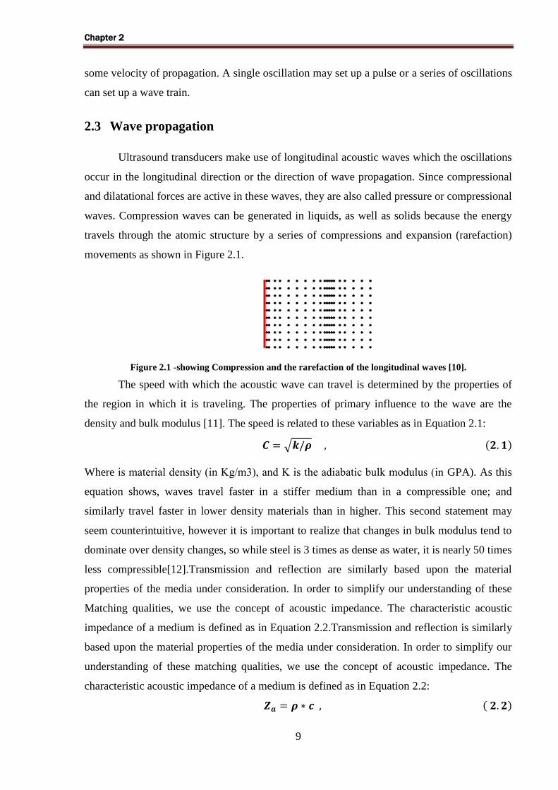
movements as shown in Figure 2.1.
Figure 2.1 -showing Compression and the rarefaction of the longitudinal waves [10].
The speed with which the acoustic wave can travel is determined by the properties of
the region in which it is traveling. The properties of primary influence to the wave are the
density and bulk modulus [11]. The speed is related to these variables as in Equation 2.1:
√ ( )
Where is material density (in Kg/m3), and Κ is the adiabatic bulk modulus (in GPA). As this
equation shows, waves travel faster in a stiffer medium than in a compressible one; and
similarly travel faster in lower density materials than in higher. This second statement may
seem counterintuitive, however it is important to realize that changes in bulk modulus tend to
dominate over density changes, so while steel is 3 times as dense as water, it is nearly 50 times
less compressible[12].Transmission and reflection are similarly based upon the material
properties of the media under consideration. In order to simplify our understanding of these
Matching qualities, we use the concept of acoustic impedance. The characteristic acoustic
impedance of a medium is defined as in Equation 2.2.Transmission and reflection is similarly
based upon the material properties of the media under consideration. In order to simplify our
understanding of these matching qualities, we use the concept of acoustic impedance. The
characteristic acoustic impedance of a medium is defined as in Equation 2.2:
( )

Chapter 2
10
Characteristic acoustic impedance, like its electrical counterpart, is a measure of the
opposition of the medium to the propagation of a sound wave. When two mediums have a
similar acoustic impedance they can be said to be “well matched” and sound waves will
transfer between them with very little reflection. For normal incident waves, this impedance
measure behaves similarly to its electrical counterpart, and reflection and transmission
coefficients for waves traveling from material 1 to material 2 can be calculated as the
following in equation 2.3 and 2.4 [18]:
,
- ( )
, - ( )
Where the acoustic impedance of the materials, R is the percent of reflected acoustic
energy and T is the percent transmitted wave energy. We can also make use of an acoustic
version of Snell’s Law to predict angle shifts in wave propagation caused by the interface Also
the transmission of sound waves across an interface between two media is most directly
described via this notion of sub- and supersonic wave crests. If a plane wave is incident onto
the interface, the point of reflection in medium 1 generates a disturbance in medium 2 (Fig.
2.2) [17]:
Figure 2.2 -Reflection and transmission at a discontinuity [17].
With sound speed c1in medium 1 and direction of incidence , sin 1) the disturbance
velocity, measured along the interface, (the phase speed) is c1 . Depending on 1and
the ratio of soundspeeds c1/c2 this disturbance moves with respect to medium 2 either super-
sonically, resulting into transmission of the wave, or subsonically, resulting into so-called total
reflection (the transmitted wave is exponentially small). In case of transmission the phase

Chapter 2
11
speeds of the incident and transmitted wave has to match (the trace-velocity matching
principle, [17])
( )
What these equations suggest is that a wide range of intuition we have gained from the
field of optics, translates directly into the field of ultrasound.
2.4 Aperture Theory and Far Field Directivity Functions.
"Aperture" in acoustics is used to refit to either a single electroacoustic transducer or
an array of electroacoustic transducers. The complex Aperture function, that is, the magnitude
and phase of the sound distribution within the aperture, determines the Fresnel and Fraunhofer
diffraction patterns of the aperture, which in turn determines the beam profile of a transducer
element. The basic equations that are derived from complex aperture theory are used to
describe the performance of a single transducer and an array of transducers. The derivations
below are not presented in their entirety [19]. These basic equations are used in the
simulations carried out in this thesis. The far-field and the near-field criterion are given by the
following two equations [19]:
, - ( )
, - ( )
Where,
√ ( )
is the magnitude of the position vector to a field point and R is the maximum range. The far
field directivity function of a general volume aperture is given by[19],
( ) * ( )+ ∫ ( ) ( )
( )
Where
( ) ( )
( ) ( )
Are the spatial frequencies
( )
( ) ( ) , ( )- ( )

Chapter 2
12
Where ( ) is the amplitude and ( )is the phase of the response at spatial location
of the aperture, both of them are real functions (The amplitude function is also called the
amplitude window)
Figure 2.3 Linear apertures of length L meters lying dong the X-axis. Also shown is a field point with
spherical coordinates (r, and ω) [19].
2.5 Beamwidth and sidelobe
To determine the far-field beam pattern, beamwidth, and the relationship between
beamwidth and sidelobe levels of far-field beam patterns, the elements are windowed i.e. each
element are given a 'weight', thus controlling the transducer response. This is called
apodization and is implemented with help of amplitude windows which are discussed next. In
general as in the rectangular amplitude window it is defined by[20]:
( ) . | | | |
/ ( )
The amplitude of the complex frequency response of the transducer is constant along
the length L of the transducer, regardless of the magnitude of frequency f with zero phases
(Figure 2.4).

Chapter 2
13
Figure 2.4-Rectangular (solid), triangular (dash) and hanning (dot) amplitude windows[20].
Or
(
)
* ( )⁄ ( )⁄ + (2.14)
.
/
* ( )⁄ ( ⁄ )+ [20]
This is the un-normalized far-field beam pattern of the hanning amplitude window.
Referring to Eq. (2.9), the normalization factor is giving by[20]
( ) . (2.15)
The normalized far-field directivity functions as defined as following[21];
(
)
.
/
( )
By substituting the previous Equations into Eq. (2.16) results in the normalized far-
field beam pattern of the hanning amplitude window (see figure 2.4);
.
/
. .
/ /
⟨ .
/ ⟩
, (2.17)
Looking at the plot for the normalized far-field beam pattern of the various amplitude
windows discussed above (figure 2.4), one sees that the first sidelobe level of the hanning
amplitude windows are approximately -23dB,while the sidelobe levels for the rectangular
amplitude windows are approximately – 13 and – 27 dB, respectively, this can be attributed to
the way the windows approaches zero at the end point x= L/2.The triangular window
approaches zero in a comparatively smooth fashion i.e. with a smaller slope than the other two
amplitude windows and hence has lower sidelobe levels. A reduction in sidelobe levels results

Chapter 2
14
in a wider main lobe; see figures (2.5), (2.6) and (2.7) show the polar of normalization far-
field beam pattern for amplitude windows discussed, as given by Equations (2.16), (2.17) and
the plots, the main lobe width is dependent on the aperture length and wavelength. The beam
width directly proportional to the wavelength λ and inversely proportional to the length L of
the aperture. The figures shows the beam patterns for two different ratios of L/λ[21].
Figure2.5-polar of the magnitude of the normalized horizontal far-field beam pattern of the
rectangular amplitude window for (a) L/λ=4, (b) L/λ=2[21].
Figure2.6-.polar of the magnitude of the normalized horizontal far-field beam pattern of the
triangular amplitude window for (a) L/λ=4, (b) L/λ=2[21].
Figure 2.7- polar of the magnitude of the normalized horizontal far-field beam pattern of the
hanning amplitude window for (a) L/λ=4, L/λ=2[21].

Chapter 2
15
2.6 Wave focusing and steering
A travelling plane wave will tend to spread from the edges as it travels using a process
of diffraction. This phenomenon is described by the Huygens-Fresnel principle, which
describes each point on a wave front as a source for an expanding radial wave. As the wave
expands, its energy is spread across a greater region. The further the wave has traveled, the
greater the reduction in wave amplitude, and the greater the reduction in amplitude of any
reflections from the wave. In order to create a high amplitude wave-front (to improve the echo
strength) the energy from the wave can be focused. Focusing the wave controls the travel path
of the acoustic energy so that its signal strength is maximized within a desired region as
shown in Figure 2.3.
Figure 2.8-Generalized sketch of a geometrically focused ultrasound path. The Solid lines show an
approximate path of constant relative strength [4].
A transducer is any object that transforms energy from one type to another. In
ultrasound we are usually interested in transforming electrical energy into acoustic energy, and
the reverse. The transducer shown in Figure 2.1 is geometrically focused, which means that
the focal point is determined by the curvature of the transducer. The same effect could also be
achieved by using an acoustic lens. In either case, the focal point cannot be easily changed,
and for this reason geometrically-focused transducers have limited use in a clinical setting. In
order to be able to control the focus, a new type of transducer needs to be considered, and a
new way of exciting it. An array transducer divides the transducer surface into sub regions,
each of which can be controlled separately through separate electrical connections. The
subdivided regions of an array are referred to as elements. When each element in an array is
excited at different times, the diffraction of the individual wave fronts generated from each
element can be planned in order to create a focused pulse as shown in Figure 2.4.

Chapter 2
16
Figure 2.9 – Timed electrical excitations create radial wave-fronts expanding from each element that
constructively interferes in order to create a combined focused wave [4].
Since it is the timing of the electrical excitation that creates the converging acoustic wave
fronts, by adjusting the pattern of delays applied, the focal region can be adjusted. This
process is called transmit focusing.
Figure 2.10 – Non-symmetric excitation patterns direct an ultrasound beam off of the transducer axis (A),
and combined with focusing produce steered focused beam (B)[3]
Array transducers also make it possible to steer the beam off the transducer axis. Beam
steering (illustrated in Figure2.5a) is accomplished by skewing the transmit delay pattern so
that it is no longer symmetric about the central axis of the transducer. The resulting ultrasound
wave front is angled or steered away from the axis. Transducer arrays that employ beam
steering as well as beam focusing are referred to as phased arrays. It should be noted that there
are practical limits to the possible steering angles that the transducer can achieve. Typically
steering angles are kept within the front 90° arc, beyond which, steering becomes difficult due
to the limited directivity of the array elements. Transmit focusing and beam steering can also
be combined so that the beam is focused along a steered path as shown in Figure 2.5b.

Chapter 2
17
2.7 Receive focusing (beamforming)
All ultrasound transducers are reversible. An electrical pulse applied to a transducer
will generate a sound wave; similarly, a sound wave incident upon a transducer will generate
an electrical signal. This is how the echoes created in the medium are received. After a sound
pulse is transmitted, the transducer begins to listen for reflections. When the reflections arrive
back at the transducer they are converted into electrical signals, and the amplitude of the
signals is proportional to the pressure of the sound wave that created them. In this case, the
fundamental frequency of the transducer acts as a carrier signal, with its amplitude indicating
the reflection size. The echo signal is extracted by taking the envelope of the received signal.
In a geometrically focused transducer, signals from the focal region will arrive at the same
time at the transducer surface, and thus create a large electrical signal. In an array, however,
the signals will all arrive at different times at each element. These situations are shown in
Figure 2.6(a) and (b).
Figure 2.11 - Receive focus beamforming a) geometric transducer b) array without delays
c) Array with delays applied to compensate for signal arrival time differences [4].
The differences in signal arrival time at each element need to be compensated for by
delaying the electrical signals after they are received. If the same transmit delays are applied
to the received signals, then waves originating from the focal region will constructively
interfere, increasing their amplitude. Signals from outside of this region will not be aligned,
and will tend to destructively interfere, reducing their impact on the final output. This process
will create the same amplitude of signal as occurs due to a geometric focus. This is
demonstrated in Figure 2.6c. The process of delaying the received signals in order to create
focus is called beamforming. Beamforming is the inverse operation of transmit focusing, so all
of the details discussed previously applying to transmit focusing, also apply to receive
focusing. In addition, since beamforming delays are applied as the signals are received, it is

Chapter 2
18
possible to change the delays during reception. Since there is a different fixed delay for signals
from different depths, we can sweep our receive focal point as the signals are collected to keep
an entire line of received data in focus during a single transmit [13]. This process of changing
the receive delays while the signal is being received is called dynamic receive focus
beamforming.
2.8 Grating Lobes
Constructive interference is relied upon to create a focused beam from an array
transducer, both during transmit and receive. However, if the spacing of array elements is not
fine enough, undesired constructive interference can occur in the imaging field. The result of
this interference is referred to as grating lobes, and occurs when the path difference between
two adjacent elements is an integer multiple of the pulse wavelength. The path difference is a
function of the element spacing, and can be approximated as shown in Figure 2.7.
Figure 2.12 - Approximation of path difference for wave incident upon transducer elements as related to
the element spacing [5].
Any energy coming from a grating lobe is indistinguishable from energy from the
actual focal region. This can cause artifacts such as ghosting in the ultrasound image. When
elements are spaced with a one wavelength separation, grating lobes will occur only along the
plane of the transducer. However, steering the beam off axis will shift the grating lobes into
the imaging region. Reducing the spacing further to half a wavelength is required to
completely eliminate their effect.
2.9 Image formation
The ultrasound diagnostic system can display the various imaging modes by receiving
and processing the various signals reflected. Among the imaging modes, B-mode (brightness
mode) is a representative ultrasound image display mode, which is expressed with reflection
intensities of tissues depending on acoustic impedance differences between the tissues. Also,

Chapter 2
19
the ultrasound diagnostic system has C-mode (color blood flow) and D-mode (Doppler
spectrum) as the major imaging modes, which display the mean velocity of blood flow using
the Doppler effect of ultrasound by moving targets. In case of a tumor in B-mode image, it is
difficult to observe a tissue having the reflection intensity not larger than those of neighboring
tissues.
Figure 2.13- Shows Different ultrasound imaging modes [10].
So, there exists an optional E-mode (elastography), which can show the mechanical
characteristics of the tissues such as tumor or cancer, and many investigations on the
ultrasound elastography are in progress. This paper describes the basic principles of B-mode
imaging process as a representative ultrasound image, present the issues of ultrasound medical
imaging, and proposes the mathematical solution on the issues, specially, the application of
elastography[62].
2.10 2D Imaging Transducers
Transducers can be made in a variety of structural arrangements. There are several
broad categories of transducer arrangement that are typically used for 2D imaging; they are
linear arrays, phased arrays, and annular arrays.

Chapter 2
20
Figure 2.14 - Array transducer types a) Linear Array b) Phased Array [5].
2.10.1 Linear Array
A linear array consists of a long strip of elements spaced with full wavelength
separation. Elements are then used in groups. Each sub group of elements is dedicated to
producing a single transmission line. Because of the full wavelength separation, beams are not
steered off of their axis to avoid grating lobes. If a fan beam is desired, the elements may be
physically arranged along a curve. A linear array transmission scheme is demonstrated in
Figure 2.12a.
2.10.2 Phased Array
A phased array is shown in Figure 2.12b. This transducer uses a strip of rectangular
transducer elements in order to produce a beam. The strip elements are spaced at half a
wavelength separation (or less). This spacing allows for off-axis beam steering without
inducing grating lobes into the field, which is how this array is primarily used [16]. The image
is made up of image lines that spread from the array over a range of angles, forming the
familiar arc sector shape. Each line in the image is usually a separate transmission focused
along an image line.
2.11 Summery
In this chapter, we described the ultrasound wave characteristics; we discussed the
equations of the wave propagation, characteristic acoustic impedance, reflection and refraction
of the ultrasound waves. .On the other hand we discussed the effect of the apodization gain
valued on both of the beamwidth and the sidelobe and we described the effect of the three
apodization types the rectangular windows, the triangular windows and the hanning

Chapter 2
21
apodization. Furthermore, we studied the wave focusing and steering and how can we use the
waves of delays to steer and focus the ultrasound beam to certain focal point and the vice
versa. We discussed how we can use the same delay shape for retrieving these waves after
being reflected from the body of concern (beamforming). Moreover we discussed the different
ultrasound imaging modes B, E, C and D. Finally we discussed both types of the 2D
Transducers which are Linear Array and Phased array transducers.

Chapter 3
22
Chapter 3
Digital Beamforming theory of operation
The ultrasound beamformer re-aligns the received signals in order to produce B-scan
lines. The method used to realign the signals, and the accuracy with which it can be
performed, affects the quality of images obtained from the system. The primary method of
realigning the signals is called the Delay and Sum method (DAS). This simply refers to the
process of delaying the signal from each channel, and summing them together. There are
many different electronic implementations that have been developed in order to realize a DAS
beamformer. In this section we, will review the common types of beamformers, and contrast
the strengths and weaknesses of each design.
3.1. Analog Beamforming
The earliest beamformers introduced delays through the addition of fixed electrical delay
lines in the receive path. The major advantage of analog (continuous time) delays is that the
signals ideally are not affected by traveling through the delay lines. These analog delays
could be implemented simply as long transmission lines, where the transmission line length
would determine the signal propagation delay. This works well at high-frequencies (> 50
MHz) but at lower frequencies the required transmission lines are prohibitively long. Instead
delays were often composed of lumped inductor capacitor (LC) circuits. This simple fixed
delay structure would not allow for the delay to be varied. In order to improve the
performance and versatility of the analog beamformer, the fixed delay line was replaced by a
tapped delay line (TDL) [26], [27]. A TDL breaks the single long analog delay into small
delay sections. By using an analog multiplexer (MUX), the signal can be brought out after
different numbers of TDL segments. Digital logic can control the MUX selection, and the
output from each can be added to provide the beamformed output. Figure 3.1a shows the
structure of a tapped-delay line analog beamformer. In order to accurately beamform the
signals using a TDL beamformer, then spacing of delay taps (and therefore the number of taps
required) must be equal to the smallest delay step tolerable.

Chapter 3
23
Figure 3.1 - Analog beamformer types, A) a delay line beamformer uses selectable fixed taps to vary the
delay on each signal B) a coarse/fine delay beamformer uses fixed taps for Coarse adjustment along with a
phase shift for fine adjustment[26].
This requires a huge amount of hardware, even for small array sizes. Furthermore, the
engineering challenge to create each TDL with perfect matching to both the analog MUX tap,
as well as following element, was significant. The Coarse/fine Analog Beamformer was
designed to address these issues. One design is shown in Figure 3.1b. This implementation
has been used in both commercial and recent research projects [28]. The coarse/fine
beamformer divides the delays into a fine delay that can be controlled with precision and a
coarse delay made up of larger TDL sections as discussed previously. The fine delay is most
commonly provided by a phase shift, rather than a true delay. This approximation works well
enough for small delays, and can be varied with great precision through a phase shift mixer.
The TDL can be implemented in a number of ways such as: LC delay lines (as discussed
previously), serial-analog memories [29], Analog shift registers, or surface acoustic wave
delay lines [30].

Chapter 3
24
3.2. Digital beamforming
Most modern systems convert the analog signals received from the transducer into a
digital form before beamforming. After conversion, beamforming can then be handled using
digital logic.
3.2.1. Classes of the Digital Beamforming
Existing digital beamforming techniques can be categorized into two classes, namely
time domain beamforming or frequency domain beamforming. These classes relate to the
domain that the echoed image data is processed or operated on. Time domain beamforming is
associated with conventional methods, whereby signals are shifted or translated in time, and is
more easily visualized by humans. Frequency domain beamforming often requires the
translation of sampled data, after A/D conversion, to its frequency domain equivalent and an
operation such as a phase-shift is performed within the frequency domain, equating to a time
delay in the time domain. The extra processing required for translation is generally balanced
with a more efficient or cost effective way of frequency domain implementation. Mucci
presented a brilliant paper describing and comparing, from a hardware perspective, the
available efficient digital beamforming algorithms from both time and frequency domains and
the advantages and disadvantages of each [31]. Although the paper is almost twenty years old,
the content and issues outlined are still more than relevant for today’s imaging systems.
Emphasis was placed on non-adaptive conventional procedures but references were still made
to more intelligent methods that utilized adaptive techniques such as phase aberration
correction. Please see appendix D for more details about frequency domain.
3.2.2. Digital Beamformer basics
The functions of a beamformer include the following [21] :
Generate transmit timing and possible apodization (the term apodization will be used as
a synonym for weighting, tapering and shading) during transmit .
Supply the time delays and signa1 processing during receive .
Supply apodization and summing of delayed echoes .
Possible additional signal processing related activities.
The goal of all of these functions is to create a narrow, uniform beam with low side lobes
over as long a depth as possible. During both transmit and receive operations. Appropriate

Chapter 3
25
delays are supplied to accomplish the focusing and steering needed. Figure 3.2 demonstrates
the geometry that is usually used.
τ
T2
T1
T4
T3
T5
Σ
τ
τ
τ
τ
Z
Axis
FP
Figure 3.2 – Shows basic geometry for beamformer calculations
Figure 3.2 also illustrates the reception process. Wavefronts are shown emanating from
a point source labeled as FP. These signals are received by the array elements, amplified and
passed on to the delay lines. The delay lines are shown as rectangular boxes whose length
corresponds to the desired delay. Finally, the echoes are passed on to the
apodization/summer stage, which takes the contributions from each element, multiplies them
with a weighting function, and adds up the results. The transmit operation is essentially the
inverse of receive focusing; time delays from a common synchronization signal are
generated by some means, often down counters, and the array elements are fired accordingly.
It is assumed the array elements act as point sources and generate the required wavefronts.
The general expression for the received echo r (t) [33]:
( ) ∑
∑ ( ( )
)
( )
In this expression, the transmitted waveshape is s(t). The A's refer to whatever weighting
function that might be applied to each of the channels during transmitting and receiving
operations. In the simplest case these would be equal to one for uniform aperture weighting.
R ( )is the distance of the source point (FP) from the center of the transducer array and c
is the velocity of the wavefront in meters per second.. Similarly, is refer to transmitting and
receive delays applied during transmit and receive beamformation operations. i and j are
indices of the receive and transmit elements, respectively, and subscripts r and x refer to
receive and transmit operations. These four parameters, , , and , will form the basis
of the discussion on beamformer evolution; changes in their values and in the methods by
which their role has ken implemented has defined the different generation of instruments.
Quality of beamformation is strongly influenced by them. Finally, in Equation 3.1, N is the

Chapter 3
26
number of transmit and receive elements and will assumed to be constant. N is also an
important factor in establishing the performance level and the cost of an ultrasound system.
Referring to Figure 3.2, the expression for determining the values for the transmitting and the
receiving delays given a desired focal point is [33]:
[√( )
] ( )
where c is the speed of sound, r, is the transmit or receive delay, , and , are the
coordinates of the point at which we wish to focus, and RB is the distance from the origin or
the phase center to that focal point. We will give a brief demonstration about the signal-
processing parameters of the ultrasound signal; accordingly, we can determine the proper
design requirements. In general, our transducer pulse signal (for 15 MHZ) will appear in the
time domain as oscillation pulse within certain period of time and will reach zero amplitude
after this time as shown in figure 3.3.
Figure 3.3- Shows 15 MHZ Transducer pulse [14].
In general, the ultrasound signal transmitted signal is determined by different
parameters determine its shape and its proper strength to reach the required body depth.
3.2.2.1. Frequency Spectrum
The transducer signal characterized by its frequency spectrum, by having a look on the
ultrasound pulse in figure 3.2, we find out that the entire transmitted ultrasound signal is
Rel
ativ
e A
mpli
tude
(dB
)/F
requen
cy
(MH
Z)
Time (usec)/Volt (mv)

Chapter 3
27
below the 20 MHZ, as well as we can notice the harmonics after 23 MHZ thus according to
the NY Quist theory, we should sample at least of 40 MHZ.
3.2.2.2. Sample Rate and Quantization
The main challenge when dealing with digitized data is the effect of quantization on the
quality of the resulting image [3]. When the signal is sampled, it is quantized in both time and
amplitude. This essentially rounds the precision of the sampled signal. The effect of this
rounding can be quite significant, when the full range of signals is considered. For time
quantization, choosing the closest sample time causes the constructive and destructive
interference to imperfectly align, reducing the output signals amplitude. The effect of
amplitude quantization is similar. Figure 3.11 shows example radiation patterns simulated
with different time and amplitude quantization levels. A secondary lobe level of around -
60dB is desirable to achieve “clinical quality” images.
Figure 3.4– Theoretical radiation patterns showing A) the reduction in secondary lobe level with slower
sampling rate time quantization B) the reduction in secondary lobe level with decreasing amplitude
quantization bit depth [3].
3.2.2.3. Signal to noise ratio (SNR)
SNR is the ratio of the measured signal to the range noise level. Our ultrasound signal
received signal is about 1.0V and the noise range is about 25mv so our SNR equal 72 db.
B A

Chapter 3
28
Figure 3.5.Shows frequency spectrum ultrasound with signal level1.0V signal noise ratio SNR.
3.2.2.4. SNR and bit depth
SNR is represented in dB, but for digital system we need bits representation
Bit depth is the number of bits used to represent that number, Relation between bit depth and
dB is:
.
/ ( )
Figure 3.6 SNR VS bit depth
3.2.3. Physical limitations
The speed with which an ultrasound pulse travels in a medium is a characteristic of the
medium material. The attenuation that a wave experiences is a combination of absorption and
scattering, is related to frequency and temperature, as well as material properties. The
Maximum Level

Chapter 3
29
attenuation in water is approximately 0.7 dB/ (cm * MHz)[12]. This effectively places limits
on the possible imaging depth achievable for a given transducer/beamformer arrangement. For
example, if the maximum system gain available is +50dB, and the ADC quantizes with 12 bits
of precision (giving ~70dB of SNR range), this gives a complete system range of
approximately 120dB for a single element transducer. So we can determine that the signal
from a 5MHz transducer would be too small to be detected at 17.1cm of depth (120/ (5MHz
*2* 0.7)).Having determined the maximum depth possible, we can then use this to determine
the maximum round trip time of flight (speed of sound in the medium is approximately the
same as water (1510 m/s) .
Using this speed we can estimate the time required for a signal to penetrate to its
maximum depth and return. Continuing the above example, it would require approximately
0.22ms (0.171m*2/1510m/s) to complete the trip. By taking the reciprocal of this time-of-
flight, we can determine another key limiting factor for any ultrasound system: the maximum
number of pulses that can be completed per second. Again to continue our example, this
system could achieve 4415 pulses per second. At real time frame rates (25FPS), this allows for
176 pulses per frame. This number is not particularly limiting for 2D imaging, unless an
unusually large number of scan lines or
3.2.4. Ultrasound digital beamforming implementations
The specific hardware selected to implement a beamformer has a great effect on the
speed, accuracy, and cost of the entire system. In general, the type of digital logic hardware
can be used to broadly categorize how beamformers approach the task. These groups are:
micro-processor based, software based, and Field Programmable Gate Array (FPGA) or
Application Specific Integrated Circuit (ASIC) based. The first delayed calculation
beamformers to be used were micro-processor based beamformers. In these systems, the
digitized data is recorded into a RAM buffer. Once recorded, a microprocessor (or similarly, a
Digital Signal Processor) is used to select the desired samples and sum them together to
produce an output image. Microprocessor technology has steadily improved over the past few
decades, increasing in speed while decreasing in price. Even with these gains, microprocessors
are inherently a serial processing device, meaning that each operation must be performed
sequentially with at most a single possible operation per clock cycle. By its very nature this
means that each additional channel adds a multiplier to the amount of time required for
processing the data, and the total time required to beamform a single line is proportional to the
Chapter 3
30
number of array elements. While microprocessor based systems have been made to handle
real-time 3D volumes of data, the required hardware was both large and expensive [36].
Another implementation of a digital beamformer that has become possible only very
recently is a software beamformer. In this beamformer, the delay and sum operations are
performed in software on a PC. Hardware is only used to digitize the signals. This moves the
bulk of the work of the beamforming process into a low cost, but high performance general
purpose processor. The major benefit of software beamformer based systems is the ease with
which they can be constructed. By making use of existing sampling cards and drivers, very
little additional hardware is required to complete the system. Further, since all data is available
on a PC environment, the difficulties of development of new experimental processing
techniques is greatly eased. Unfortunately, these systems are bandwidth limited, even using
modern PCIe buses. An average PCIe (2.0, x8) bus in a current generation system can support
a theoretical maximum 4GB/s transfer rate, with implemented versions achieving far less.
This speed is sufficient for 40 channels of high-speed ADC data (65Ms/s, 12bit), with
marketed versions falling far short of the theoretical transfer rate. Because of these
limitations, it is not currently possible to conduct high-speed, high-channel beamforming
using these systems. Beyond this, the sampling hardware is sufficiently expensive itself to
offset the cost of the savings by using PC beamforming with larger systems. This option
remains viable for fast development with low speed, and arrays with a small number of
elements.
Either an FPGA or ASIC device is capable of implementing a hardware based
beamforming method. An FPGA is a hardware chip that is comprised of reconfigurable logic
circuits. The physical hardware connections within the device can be reconfigured so that its
digital logic functions are arranged to perform nearly any logical operation desired. By
contrast an ASIC is designed at a silicon level to perform the desired series of operations, and
manufactured to only include the necessary logic for its original design. ASICs are
significantly more expensive to both design and develop, but can produce cost savings when
produced in large batches.
ASICs are mainly used by larger companies. In both devices the approach to
beamforming is the same. The beamforming operations are performed using digital logic
gates, in each device. By its nature, digital logic is parallel, and pipelined for high throughput.
For ultrasound beamformers, this results in extremely high-speed performance. Also, since
each channel is processed in parallel, additional channels require more hardware to process,
but the processing time remains almost the same. The main limitation of ASIC and FPGA

Chapter 3
31
designs is their complexity to produce. They require a significant amount of support circuitry,
and can take a long time to develop and debug.
3.2.5. Digital beamforming Development
The idea of building a platform for research is not new. There has been a need in the
ultrasound community for this type of application for a number of years [37].
Up until very recently, there have been no options available. Over the past few years, however
a few companies have started to produce flexible beamformers to fulfill this role. This section
will trace the development of digital beamformation. We will start from the very early designs
and work our way towards the present.
3.2.5.1 Digital beamforming Earlier Development
The earliest works on use of digital control for delays appeared in 1975 [38]. A
technique was developed for use of charge coupled devices (CCD) to provide programmable
time variable analog signal delay for scanning a linear ultrasonic phased array. This technique
had dynamic focusing depths of 2 to 40 cm. The element delays were controlled by a 8080
microprocessor. Figure 3.6 shows the system operation of the earliest attempt at digitally
controlling delays.
Figure -3.7 Simplified system operation of earliest attempt at digitally controlling delays [38]
Even though digital control was used to control delays, the concurrent use of analog delay
lines created major problems in imaging like image artifacts. This led to the development of
electronic delay lines and new techniques for dynamically varying the electronic delay lines.
For the first time, the concept of sampled data systems was used to implement circuits for
electronic delay lines [38]. The underlying principle behind these delay schemes involved

Chapter 3
32
buffering the sampled data in a memory with independent read-write ports. The stored
samples are read out after an appropriate number of clock cycles to generate an on-line,
pipeline delay (Figure 3.7a).
Figure -3.8a Principle OP digital delay line [32]
Another variation of implementing a delay line was also described [32, 39]. A FIFO
(first in first out) device in conjunction with a RAM memory was used. The FIFO eliminates
the addressing circuitry needed for RAM implementation. The delays thus implemented are
long with high precision broad bandwidth and minimum phase distortion. Furthermore, the
development and refinement of IC electronic components made these schemes attractive.
Figure 3.7b shows the general architecture of digital beamformer implemented.
Figure 3.8b- Phased array ultrasound system with digital delays[39]
Figure 3.8 is a block diagram of earliest digital system constructed where al1 analog circuitry
is replaced by digital circuitry [39]. In this 16-channel system, the microprocessor controller
fixed the times at which each transmitter sends an electrical pulse to its transducer element, to
steer the acoustic signal in the desired direction. The echo signals after amplification are
digitized and fed to a digital delay circuit consisting of FIFO memory element.

Chapter 3
33
Figure 3.9- Block diagram of the ultrasonic imaging instrument when the analog circuitry is replaced by
digital circuitry [39].
The delay in this element was controlled by the microprocessor to provide focusing
and steering at the receiver. The signals were then summed together to form the reconstructed
image. One of the major problems in medical ultrasound imaging was the imaging of the
dynamic movements of organs such as the hem. The systems that were developed made use of
one delay Line per channel, providing the required delay in a discrete quasi-continuous
manner. Each delay line provided hundreds of delay taps to provide the overall delay. So real-
time scanning of the heart required fast switching to continuously track the echoes, which
required an especially complex control system and introduced undesirable switching noise. In
order to track the variable returning echoes efficiently, novel methods for implementing a
programmable delay system were developed [40, 41]. The technique was based on separate
and independent processing of the carrier and of the envelope of the echo pulses. Carrier
phasing was accomplished by electronic phase-shifters, while delay lines varied the envelope
delay. The approach adopted was based on mixing the echo with a digitally phase-controlled
coherent local oscillator, followed by filtering of the upper or of the lower sideband. Once
phase coherence of signals was established, the increment of the delay line required for time-
shifting the signal envelope is no longer dependent on the carrier frequency value , but on
the extent of signal bandwidth around . O'Donnell et. Al., [42] proposed a digital
beamformer with autonomous channel control in place of the conventional delay and add
architecture. The fully digital beamformer used the principle of baseband interpolation. A
block diagram of the processing performed on each channel is presented in Figure 3.9.

Chapter 3
34
Figure 3.10 - Fully digital beamformed using baseband interpolation [42].
The digital baseband interpolation algorithm uses baseband demodulation followed by
Low pass filtering and phase rotation to implement the delays. The phase is rotated using a
CORDIC processor. While the earliest commercially available digital beamformers were
available in the early 80's, they did not begin to have significant impact until the early 1990's.
Much of this delay was due to the need for A/D converters (ADC) with sufficiently large
number of bits and a high enough sampling rate for ultrasound signal digitization. In the
designs discussed above [32, 41], 8-bit A/D converters were used which limited the using
quantization of delay as well as the pulse fidelity. They tried to overcome this problem by
analog shift registers [32] or by phase shifting [41]. Therefore an obviously important topic is
the number of bits required for A/D conversion. The literature does not supply a real answer.
Most expressions given are constrained by the assumptions mad. Now 12- bit A/D converters
have been developed, thus increasing the dynamic range.
3.2.5.2 Digital beamforming existing technology comparison
In this section we will review the commercially available beamformers, and contrast
them against the design developed in this thesis. Although most of these systems have been
released since the beginning of this thesis work, each of them contains a number of trades-offs
that make them unsuitable for our application. The majority of commercial development has
focused on extracting raw sample data from a commercial system for post-processing. This
serves the needs of a segment of the ultrasound community that is developing post-processing
algorithms, but ignores the requirements of those working on transducer designs and front-end
processing techniques. This trend began with the development of Ultrasound Research
Interface (URI). The original URI was developed in 2003 by Siemens as an extension to their
SONOLINE Antares Scanner, and was called the Axius Direct URI. Since that time, Siemens,
GE, and Philips/ATL, have all produced add-on interface cards for researchers to access some
parts of their system hardware. Most of these systems are not comparable to this thesis work
as they do not allow the use of custom transducers, and contain a highly restricted interface.

Chapter 3
35
In the last few years, Ultrasonix has made the open nature of its platform a selling
feature. This began with the 500RP [43]. This platform contained a fixed number of channels
(32) and a fixed sampling rate (40MHz), but allowed low level access to the beamformer
through an open API framework. The system was still expensive ($65k-$100k USD), and
could not support either the channel count or frame-rate required by some systems in our lab
(288 channels, real-time 3D). Their more recent effort is the Ultrasonix SonixDAQ and
SonixTOUCH Research system released in 2010[28][25]. The SonixDAQ is an add-on
module to the SonixTOUCH that is intended as a data collection tool. The module can support
a large, but fixed, number of channels (128), to capture a large, but fixed, buffer of data
(16GB). The module is limited in that its external download link is restricted to USB 2.0
speeds, and is not intended for real-time processing of volumetric data. The SonixTOUCH
itself can only be used with transducers it is designed for, and the processing hardware cannot
be adjusted to account for transducers with differing numbers of elements. In addition, the cost
of the SonixDAQ system ($70-80k) is added on to the already high price of the base system.
The other major development in research platforms comes from developments in
software beamformers. In 2007 Vera Sonics announced a commercially available software
beamforming platform the Vera Sonics Ultrasound Engine [46]. This system can support a
maximum of 64 channels, although only at reduced sampling rates. In comparison with the
amount of data throughput used on a standard channel in this thesis, only 8 channels would be
supported. This system is not competitive with the channel count and data rate required for our
applications, and furthermore, would require additional layers of hardware to interface with
our transducers.
Outside of commercial developments, individual research groups have contributed their own
beamformer system designs to the store of academic knowledge available. C. Hu et al.
developed an FPGA based high-frequency beamformer [47]. Their design was only for low
channel count devices, and due to a low-speed USB PC connection, only for offline or 2D
processing. The same group earlier this year reported a mixed analog-digital based system
replacing their earlier design [48]. The design uses a commercial ADC capture board that
digitizes RF data from an analog beamformer front-end. They were able to beamform a 64
element high frequency array at 400fps. This system is still restricted to 2D, and contained a
fixed number of channels. The analog nature of the design also places considerable restrictions
on the applications of the system; for example, parallel beamforming is impossible with this
design, as is supporting lower frequency transducers.

Chapter 3
36
Yasutaka et al. [49] have reported a high-speed FPGA based beamformer design, although no
hardware has yet been produced. JA Jensen and S. Nikolov et al. have also reported several
hardware beamformer designs. Most recently, they have begun to construct a large hardware
capture beamformer [50], [51]. The hardware specifications presented have been impressive,
however the design has not yet been presented as complete. Also the cost of the complete
system places it out of reach of most researchers. In addition, many researchers have begun to
attempt to use software based beamforming systems, however all have experienced the
drawbacks described in the previous section [52].
In addition to the shortcomings given in the systems above, all of the shown solutions
fail to be effectively scalable to support both large and small designs. If a system is designed
for transducers with few elements intended for low-speed imaging, it is not expandable to
high-end designs. If a system targets transducers used for high-speed imaging, it does not
scale for use with low-end systems. The system given in this thesis provides an ideal match for
both high-channel count designs for high-speed imaging, as well as the opposite end of the
spectrum in low-cost, low-channel systems, due to its inexpensive and versatile design.
3.3 Summary
Beamformer design has been an integral part of the ultrasound system since the
technology was conceived. We discussed in this chapter the meaning of the analog
beamforming and the digital beamforming and described the advantages and the disadvantages
of both. Furthermore, we discussed the main features of ultrasound digital signal processing
by studying the ultrasound pulse Frequency Spectrum, Sample Rates, (SNR)Signal to noise
ratio, Digitalization and Bit Depth, Arithmetic precision and Signal band width and Sampling
rate also we studied the ultrasound digital beamforming different ways of implementations. At
the end of the chapter we made a comparison between the existing technologies of the digital
beamforming designs.

Chapter 4
37
Chapter 4
Ultrasound Digital Beamformer Hardware Design
4.1. Introduction
This chapter will describe the design of a digital beamformer Hardware. We will start by
describing an overview of the complete hardware design, and how the different functions are
segmented into separate hardware. Next, the hardware component choices made, and each of
the hardware sections is discussed in detail to describe the key features of each design. Finally,
the cost required to produce each board is detailed.
4.2. Hardware Design Requirement
The beamformer design will need to excel in a number of areas. First it must be
reconfigurable. This reconfiguration needs to allow it to create a nearly arbitrary image region,
and should have the ability to vary nearly every parameter involved in the beamforming
calculations. The device should also be reconfigurable on-the-fly, with no knowledge of
hardware internals. Secondly, the design should be expandable or contractible, to fit with the
size of device needed. Again this expansion and contraction should not require any
understanding of the hardware internals. Thirdly, the system should be high-speed. This is
required to allow for modern 3D and real -time 3D imaging. Finally, it should be inexpensive,
with the cost scaling by the number of channels required for any given task. In addition to
these requirements, it was our intention to make this design as high-quality as possible. Well-
designed hardware can be difficult to identify, as it involves not just one area, but every part of
the design process [53], [54]. A good design is not only tightly integrated, and elegantly
arranged, it is also intentional in how these details are handled [3].
4.3. Hardware Design Architecture
When the complete beamformer system was initially conceived, the most important
consideration was how the signals will flow through the system. Typically, signals arriving at
the beamformer from a single group of wires, or connector, will need to be spread apart for
processing, and then routed back together for summation and display [3]. Figure 4.1 shows
the three-dimensional arrangement of processing boards we used in order to solve this
problem.
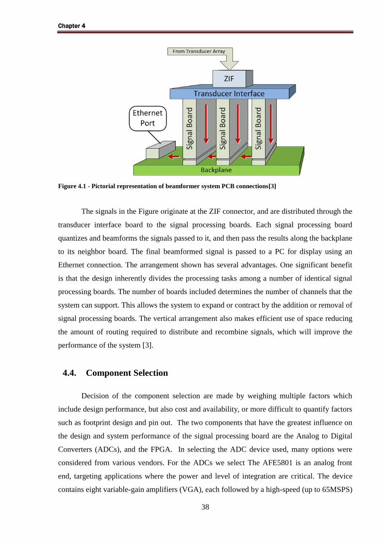
Chapter 4
38
Figure 4.1 - Pictorial representation of beamformer system PCB connections[3]
The signals in the Figure originate at the ZIF connector, and are distributed through the
transducer interface board to the signal processing boards. Each signal processing board
quantizes and beamforms the signals passed to it, and then pass the results along the backplane
to its neighbor board. The final beamformed signal is passed to a PC for display using an
Ethernet connection. The arrangement shown has several advantages. One significant benefit
is that the design inherently divides the processing tasks among a number of identical signal
processing boards. The number of boards included determines the number of channels that the
system can support. This allows the system to expand or contract by the addition or removal of
signal processing boards. The vertical arrangement also makes efficient use of space reducing
the amount of routing required to distribute and recombine signals, which will improve the
performance of the system [3].
4.4. Component Selection
Decision of the component selection are made by weighing multiple factors which
include design performance, but also cost and availability, or more difficult to quantify factors
such as footprint design and pin out. The two components that have the greatest influence on
the design and system performance of the signal processing board are the Analog to Digital
Converters (ADCs), and the FPGA. In selecting the ADC device used, many options were
considered from various vendors. For the ADCs we select The AFE5801 is an analog front
end, targeting applications where the power and level of integration are critical. The device
contains eight variable-gain amplifiers (VGA), each followed by a high-speed (up to 65MSPS)

Chapter 4
39
ADC, for a total of eight ADCs per device. Each of the eight differential inputs is buffered,
accepts up to 2Vpp maximum input swing, and is followed by a VGA with a gain range from
–5dB to 31dB. The VGA gain is digitally controlled, and the gain curves versus time can be
stored in memory integrated within the device using the serial interface.
Typically, FPGA beamformer designs are limited by RAM resources as well as the
number of I/Os available on the FPGA device. In evaluating the available options, only Xilinx
devices were considered due to previous design experience with their products. The latest
devices released at the start of this design were the Xilinx Virtex 6, and Spartan 6 series
devices [55], [56]. Both of these series of devices use 40/45 nm lithography CMOS and have
lower power consumption than previous generations [57]. Both also make use of an advanced
configurable logic block (CLB) design that allows six input look up table (LUT) connections
compared to four input LUTs of previous generations. This increase results in more compact
and efficient device routing. The major difference between the Virtex and Spartan devices is
that the Spartan series is optimized for cost, while the Virtex series is optimized for
performance. The Virtex typically offers higher clock speeds, and some additional advanced
features such as hardware MAC Blocks, HTX transceivers, and faster maximum clock speeds
compared to the Spartan, but at added expense. For the beamformer architecture, none of these
additional features were critical, allowing the choice of a Spartan series device for this design.
When the Spartan 6 product table is considered [58], the most common and versatile
package used is the FGG484 package. One advantage of this package is that it makes use of a
1mm pitch Ball Grid Array (BGA) footprint. Additionally, the FGG484 footprint is available
as an option for devices as small as the LX25 device (24k available logic cells), to the largest
LX150 and LX150T devices (147k available logic cells). Each of the devices is drop-in pin
compatible with others of the same footprint, provided that the additional I/Os available in
larger sizes are not used. However, for the cost saving factor, we select LX45 as our design
package besides, we used the Atlys Spartan 6 FPGA Development board as our testing board a
pictorial diagram for the board shown in Figure 4.2.

Chapter 4
40
Figure 4.2-The Digilent Atlys Spartan 6 FPGA Development Kit[62]
The on-board collection of high-end peripherals, including Gbit Ethernet, HDMI
Video, 128Mbyte DDR2 memory array, audio and USB ports make the Atlys board an ideal
host for complete digital systems built around embedded processors like Xilinx’s MicroBlaze.
Atlys is fully compatible with all Xilinx CAD tools. Also we are taking the TI Digital
beamformer design as our reference design which is used DSP C64+ which Digital signal
processor With performance of up to 5600 million instructions per second (MIPS) at a clock
rate up to 1.2 GHz.C64x+ core offers solutions to high-performance DSP programming
challenges. The DSP core possesses the operational flexibility of high-speed controllers and
the numerical capability of array processors.
4.5. Digital Beamformer Hardware Design
The Hardware design is comprising of IP cores (Written by HDL) inside the FPGA
interfacing with the other hardware by special interfaces and managed from the upper layers
by a software processor (MicroBlaze). In this section, we will describe the FPGA banks and
its interfaces with the outside world, as well as we will discuss the different system interfaces
and its flow furthermore we will describe in brief the MicroBlaze architecture and its main
components. We will illustrate the power section which responsible to generate the required
power for all the system also we will illustrate the DDR2 memory system attached to the

Chapter 4
41
FPGA which used for buffering the (delayed) data. At the end of the section we will describe
the analog front end, including the transmitter circuit, receiver circuit and switches with
isolators as well. Figure 4.3 shows the system design architecture:
Spartan-6
AX
I BU
S
MicroBlaze
BeamFormer
Brain
Receive Beamformer
IP
Cybress DDR2
LVDS
Interface_1AFE5804_1
LVDS
Interface_8
LVDS
Interface_1AFE5804_2
LVDS
Interface_8
16 channel
Receiver AFE
SPI
Interface
TX810_1
TX810_2
16 channel T/R
switches
LM96550_1
16 channel
Pulsers
1
2
3
63
64
16 channel
Probe
PowerSupply
Transmitt Beamformer
IP
Beamformer Control
IP
Receive Beamformer
IP
Transmit Beamformer
IP
ADC
ADC
ADC
ADC
LM96550_8
LM96570_1
16 channel
Transmit beamformer
LM96570_8
UWire
UWire
P
N
P
N
MPMC
memory
controller
IP
Uwire
Interface_1
Uwire
Interface_8
MAC
IP
PHYEthernet
Port
AXI PCI
Bridge
BackPlane
FlashMemory
Figure 4.3-Digital Beamformer system architecture
4.5.1. Overview
As we described before in figure 4.3, the proposed system architecture was designed
for beamforming 16 channels, and it comprises two transmit beamformer ICs (LM96570)
acting as pulse pattern control followed by two ultrasound pulser driver ICs (LM96550) this
was for the transmitter circuit. For the receiver circuit, there are two ICs (AFE804) comprising
all the receiver AFE functionality, both of circuits is isolated by HV switches. In the FPGA
side, we can find two IP core controllers the receiver / transmitter circuits and there is control
IP core synchronize between the transmitting and the receiving as well as control the HV
switches. Besides there is PCI Bridge for interfacing with the backplane, as well as there is a
memory controller for DDR2 operation controlling. The last interface is the MAC, and this is
the responsibility of the MAC IP core. All the software operation (FSM) is managed by the
MicroBlaze software processor through AXI bus. There is custom circuit consisting of a
number of DCDC regulators for powering up the digital beamformer system.

Chapter 4
42
4.5.2. Power system
One of the main points of failure of the Digital beamformer system was the power
distribution system. In our designed, we are using three switched mode power supply. A
switched mode power converter is a modern DC-DC converter design that uses a pair of
matched power field effect transistors in order to regulate an input DC power supply into a
different voltage with high conversion efficiency [59 - 61]. The input power rail for this
design is 5V voltage regulator circuits from Linear Technology create the required 3.3V, 2.5V,
1.8V, 1.0V, and 0.9V supplies from the main 5V supply. The switch mode converters were
designed using a buck converter topology. Please see appendix A for more details about the
schematics.
Figure 4.4- Digital beamformer power section [62].

Chapter 4
43
4.5.3. FPGA
The Spartan 6 series FPGA provides the processing for each channel of digitized
data. We are using VHDL as the internal hardware definition language (HDL) code, which
defines the operation of the FPGA. Here I will present the FPGA hardware features. As the
processing center of the card, the FPGA receives signals from, and delivers them to, multiple
sources on the board. In the FPGA Banks section comprising the four banks of the
SPARTAN 6 FPGA. These banks are controlling the whole operation of the digital
beamformer as shown in the next figure,
Spartan 6
FPGA
BANK 0
BANK 2
BANK 1
BANK 3
ADC 0-7
Pulsers & SW 0-7
ADC 8
-15
Pul
sers
& S
W 8
-15
DRAM
Ethernet
SPI Flash
Configuration
JTAG
Figure 4.5 – Diagram showing major FPGA I/O bus connections per bank. ADC busconnections attach to
Banks 3 and 0. Data is passed in to the card along the backplaneconnections to Bank 1, while beamformed
data is passed out on Bank The Comm 2.bus is bidirectional, and attached to Bank 2. DRAM pins are
allocated in Bank 1[62].
Please see more details about the schematic in appendix A, as the processing center of
the card, the FPGA receives signals from, and delivers them to, multiple sources on the board.
-0=/874Figure 4.5 shows the major bus connections that are handled by the FPGA, and
indicates the I/O bank to which they are attached. I/O banking rules for the Spartan 6 devices
can be complex [64], and the existing arrangement was created in order to accommodate those

Chapter 4
44
rules, as well as to minimize the overall layout paths for each major bus. The highest speed
bus signals (387MHz DDR) are generated by each of the ADC chips. Incoming transducer
signals are passed to the FPGA through the ADC chips. The interface between the FPGA and
each ADC device consists of 8 differential high-speed DDR LVDS signals, each differential
pair containing a serial stream of data for a single transducer channel. Each ADC also
transmits a high-speed serial clock that is synchronous to the serial data, and a lower speed
frame clock that is synchronous to the beginning of each data word from the ADC. Both of
these signals are also transmitted using LVDS.
The final bus shown in Figure 4.5 is the JTAG input bus. This is not associated with
any input bank as it is only used to initialize the FPGA hardware when the power is turned on.
The JTAG bus connects the FPGA to a Xilinx based flash electronically erasable
programmable read-only memory (EEPROM) chip (XCF32P). The EEPROM stores the
synthesized HDL code used to initialize the hardware state of the device, and can be
reprogrammed through a JTAG port on the board. It should be noted that this port is operated
as a serial master device, using the onboard oscillator circuit to control the programming
sequence. This is in contrast to the more common mode in which the EEPROM is operated as
a serial slave device. The serial slave mode is hardware selectable using an optional resistor
connected to the Mode Select pin (R7/R8). It has been designed this way to make use of the
hardware compression feature of the EEPROM. Hardware compression is required in order to
fit the full configuration file for the largest LX150 device into the EEPROM. Aside from the
hardware signal buses, the FPGA contains two oscillator mounting points, only one of which
is used in the current design, with the second provided for future expansion. A signal is also
provided to indicate the presence (or absence) of the previous card in the chain. The FPGA is
supported by a large number of decoupling capacitors mounted on the reverse side from the
FPGA, and incorporated into the BGA via footprint. Please see the appendix A for more
details about the schematics.
4.5.4. DDR2 Memory
A single 1Gbit DDR2 memory chip is driven from the memory controller block in the
Spartan-6 FGPA. The DDR2 device, a Micron MT47H64M16-25E or equivalent, provides a
16-bit bus and 64M locations. The DDR2 interface follows the spinout and routing guidelines
specified in the Xilinx Memory Interface Generator (MIG) User Guide. The interface supports
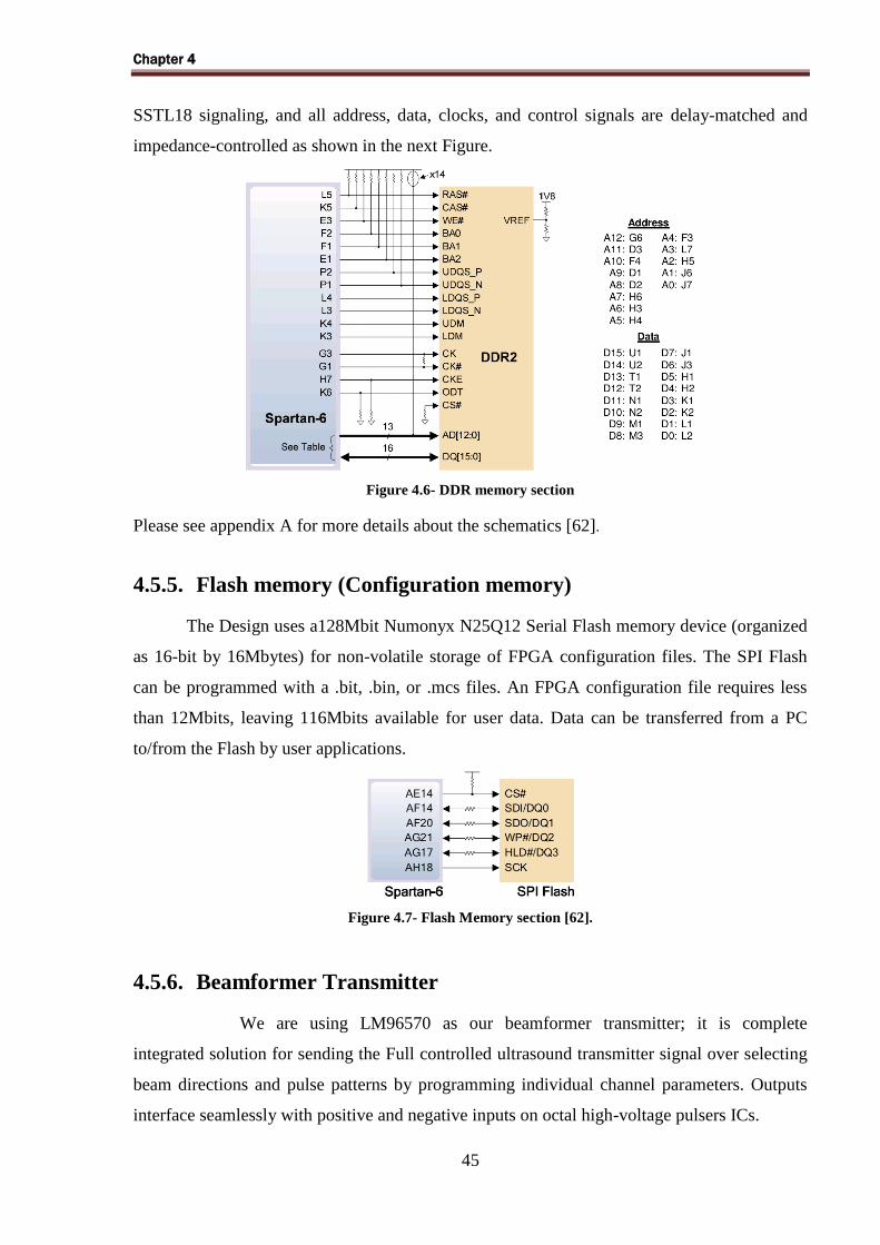
Chapter 4
45
SSTL18 signaling, and all address, data, clocks, and control signals are delay-matched and
impedance-controlled as shown in the next Figure.
Figure 4.6- DDR memory section
Please see appendix A for more details about the schematics [62].
4.5.5. Flash memory (Configuration memory)
The Design uses a128Mbit Numonyx N25Q12 Serial Flash memory device (organized
as 16-bit by 16Mbytes) for non-volatile storage of FPGA configuration files. The SPI Flash
can be programmed with a .bit, .bin, or .mcs files. An FPGA configuration file requires less
than 12Mbits, leaving 116Mbits available for user data. Data can be transferred from a PC
to/from the Flash by user applications.
Figure 4.7- Flash Memory section [62].
4.5.6. Beamformer Transmitter
We are using LM96570 as our beamformer transmitter; it is complete
integrated solution for sending the Full controlled ultrasound transmitter signal over selecting
beam directions and pulse patterns by programming individual channel parameters. Outputs
interface seamlessly with positive and negative inputs on octal high-voltage pulsers ICs.

Chapter 4
46
Figure 4.8-Digital beamformer transmitter IC [65].
Pulse patterns are locally generated with Sequences of up to 64 pulses
Adjustable Pulse widths. So we can find with fewer signal interfaces we can have a complete
four digital beamformer transmitter with 16 channels by 2 of them only. We are using 2 of
them are being used in our design controlling by the Uwire IP core as shown in the next
Figure.
FPGA
Spartan 6
LM96570
TX Beamformer
LM96550
pulserRegisters
Clock engine
Le
ve
l S
hif
ter
LM96570
TX Beamformer
LM96550
pulserRegisters
Clock engine
Le
ve
l S
hif
ter
U Wire
U Wire
SW
SW
Figure 4.9-Digital beamformer transmitter interface with FPGAPlease see the appendix A for more details
about the schematics.
4.5.7. Beamformer Receiver
The AFE5801 is an analog front end, targeting applications where the power and level
of integration are critical. The device contains eight variable-gain amplifiers (VGA), each
followed by a high-speed (up to 65MSPS) ADC, for a total of eight ADCs per device.

Chapter 4
47
Figure 4.10- Digital beamformer receiver IC architecture[68].
Each of the eight differential inputs is buffered, accepts up to 2Vpp maximum input
swing, and is followed by a VGA with a gain range from –5dB to 31dB. The VGA gain is
digitally controlled, and the gain curves versus time can be stored in memory integrated within
the device using the serial interface. A selectable clamping and ant aliasing low-pass filter
(with 3dB attenuation at 7.5, 10, or 14MHz) is also integrated between VGA and ADC, for
every channel. The VGA/ant aliasing filter outputs are differential (limited to 2Vpp) and drive
the onboard 12bit, 65MSPS ADC. The ADC also scaled down its power consumption should a
low sampling rate be selected [68]. The ADC outputs are serialized in LVDS streams, which
further minimize power and board area as shown in the next Figure
FPGA
Spartan 6
AFE5804_1
Registers
Clock engine
AFE5804_2
Registers
Clock engine
SW
SW
LVDSAnalog
Signal
LVDS
Analog
Signal
LVDS
LVDS
SPI
SPI
Figure 4.11- Digital Beamformer receiver interfacing with FPGA
Please see the appendix A for more details about the schematics.

Chapter 4
48
4.6. Cost analysis
There are three primary expenses in a typical printed circuit board construction that
need to be considered: the cost of the components, the cost of the circuit board, and the cost of
assembly (or build-up). For the boards built for the imaging system in this thesis, the
component costs dominate the expenses, although PCB construction and build-up costs are the
more variable of the three. These costs would be reduced in volume production. We could not
reach with our design to the manufacturing process, but we will have another manufacturing
process for the digital beamformer as cost analysis reference for similar design except, they
are using older and discrete chips, which cost more not like our design, which based on the
integrated solutions also in their board. They used Xilinx SP605 Board, which cost around
500$ but for us our diligent board cost 200$.
Table 4.1 - Cost summary for 64 channel systems[3]
The digital signal board is the most expensive portion of the system, since it contains both the
beamforming logic FPGA and ADC units. Their components on a single board were
purchased for a combined price of approximately $560 Canadian dollars per board. The PCB
was produced for $77 per board. Two components required assembly from outside of the lab,
the FPGA, and TQFP ADC units. The overall system cost per channel of data decreases as
more channels are added to the system as shown in Figure 4.13.
Figure 4.12- System cost per beamformer channel compared as the size of the system isincreased[3].
For a small system of 32 channels or less, the cost is approximately $40 per channel, while
as the system size increases, per channel costs decrease to just under $25 per channel.

Chapter 4
49
4.7. Summery
The proposed system architecture was designed for beamforming 16 channels. We
discussed the overall architecture with highlighting the concept of multiple board integrations
by one backplane. In general, the HW design comprises two transmit beamformer ICs
(LM96570) acting as pulse pattern control followed by two ultrasound pulser driver ICs
(LM96550) this was for the transmitter circuit. For the receiver circuit, there are two ICs
(AFE804) comprising all the receiver AFE functionality, both of circuits is isolated by HV
switches. In the FPGA side, we can find two IP core controllers the receiver / transmitter
circuits and there is control IP core synchronize between the transmitting and the receiving as
well as control the HV switches. Besides there is PCI Bridge for interfacing with the
backplane, as well as there is a memory controller for DDR2 operation controlling. The last
interface is the MAC, and this is the responsibility of the MAC IP core. All the software
operation (FSM) is managed by the MicroBlaze software processor through AXI bus. There is
custom circuit consisting of a number of DCDC regulators for powering up the digital
beamformer system we go through the hardware design of the digital beamformer. We
referenced our full detail HW schematics in the appendix.

Chapter 5
50
Chapter 5
Ultrasound Digital Beamformer Firmware Design
5.1. Introduction
Our proposed design is based on the field programmable gate arrays (FPGAs) in order to
beamform the sampled transducer echo signal. Unlike ASIC designs, FPGA devices can be
reprogrammed to perform different tasks. Because of its role in the system, the firmware
design is just as important as the hardware design in determining system performance. We will
describe in details the implementation the low level design of our digital beam former design
by describing in details the design details for the composed components of the digital
beamformer system the transmitter digital beamformer, receiver digital beam former and the
controller.
5.2. Background
In this chapter we will review how FPGAs function, and the role of hardware definition
language (HDL) in producing a successful design. We will then describe the full system HDL
modules used in this system and how they interact to create a beamformed image. Some of the
key design features, along with their implementation details will then be reviewed. We will
demonstrate the synthesis performance results achieved by the design, and finally review the
HDL verification procedures.
5.2.1. FPGA
At its simplest level, a field programmable gate array (FPGA) is a reconfigurable logic device.
The earliest versions of these devices provided little more than cross point connections
between logic gates to define controllable logic. Modern FPGA devices use a mixture of
configurable logic blocks (CLBs), which provide logic elements, MUXs and look up tables
(LUT s), Block RAM buffers, Clock Managers, specialized single function hardware, and
routing [69-71]. The connections between these elements are controlled so they can be
configured in a nearly unlimited number of ways as shown in Figure 5.1.When the system is
turned on, the hardware is programmed using a downloaded hardware definition file. The
hardware definition file contains a description of how each hardware element needs to connect
itself. During this initialization phase, the hardware cannot be used until the entire device is
programmed.

Chapter 5
51
Figure 5.1-Shows the interconnection between CLBs [49].
One key benefit of an FPGA design is that since the hardware is reprogrammed at each
time power is applied, the hardware state can be changed by altering this programming file. It
is therefore possible to modify the FPGA code without making hardware changes.
5.2.2. Verilog HDL
The hardware definition file used to program an FPGA device is generally referred to
as firmware. This file is written in such a way that each bit refers to a specific functional logic
selection within the FPGA. In order to generate this file, a higher level description of the
desired hardware logic must be created and processed. This high level file is written in a
language called a hardware definition language (HDL). The HDL used in this development is
the Verilog HDL language. Verilog is based on the “C” computer programming language
syntax and structures. Much like in the C programming language, Verilog builds up a design
by defining modules. Each module defines logic operations that occur within it, as well as
defining any sub-modules used. A top level module contains the whole design. Unlike in a
programming language where all operations are sequential, in a HDL all defined logic
operations occur simultaneously and continuously, dependent on the logic structures built.
Once a complete design is created in an HDL parsing that code is the next step to fit it into a
specific FPGA device. There are several steps in this conversion process.
5.2.3. FPGA Synthesizing Process
There FPGA flow is mainly composed of five major phases, which are: RTL (or
schematic drawing or IP porting), Functional Simulation, Synthesizing, Place and routing and
finally Programming and testing. These phases are shown in Figure 5.2.

Chapter 5
52
Figure 5.2.Shows the FPGA Design Flow [73].
First the HDL code must be synthesized, which converts it from a high level
description to a gate level implementation. This also confirms that the HDL as written does
have a hardware equivalent. The next stage is mapping, which takes the gate level description
and assigns it into the hardware structures that are actually available in the chosen FPGA.
Finally, the design must be placed and routed. This takes the mapped design, assigns it into
specific hardware, and determines the path routes required to connect all of this logic. The
place and route process also includes optimization, in which the design is rearranged to
improve the distribution of the assigned hardware, to improve signal timing.
5.2.4. Re-programmability
The use of an FPGA in any system, allows the hardware to be reprogrammed.
The steps involved in reprogramming an FPGA device have been detailed in the previous
section. In general, reprogramming an FPGA requires a high degree of knowledge of the
hardware and a complete understanding of the currently implemented firmware design.
Spartan 6 FPGA is characterized by its volatile memory, which means once the FPGA is being
under reset, all logic inside will be erased. Thus, the need of non-volatile memory (SPI flash
memory) has been raised in this kind of FPGAs. After resetting the FPGA it reconfigures itself
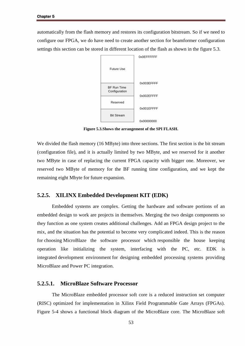
Chapter 5
53
automatically from the flash memory and restores its configuration bitstream. So if we need to
configure our FPGA, we do have need to create another section for beamformer configuration
settings this section can be stored in different location of the flash as shown in the figure 5.3.
0x00000000
0x001EFFFF
0x0EFFFFFF
0x002EFFFF
0x003EFFFF
Bit Stream
Reserved
BF Run Time
Configuration
Future Use
Figure 5.3.Shows the arrangement of the SPI FLASH.
We divided the flash memory (16 MByte) into three sections. The first section is the bit stream
(configuration file), and it is actually limited by two MByte, and we reserved for it another
two MByte in case of replacing the current FPGA capacity with bigger one. Moreover, we
reserved two MByte of memory for the BF running time configuration, and we kept the
remaining eight Mbyte for future expansion.
5.2.5. XILINX Embedded Development KIT (EDK)
Embedded systems are complex. Getting the hardware and software portions of an
embedded design to work are projects in themselves. Merging the two design components so
they function as one system creates additional challenges. Add an FPGA design project to the
mix, and the situation has the potential to become very complicated indeed. This is the reason
for choosing MicroBlaze the software processor which responsible the house keeping
operation like initializing the system, interfacing with the PC, etc. EDK is
integrated development environment for designing embedded processing systems providing
MicroBlaze and Power PC integration.
5.2.5.1. MicroBlaze Software Processor
The MicroBlaze embedded processor soft core is a reduced instruction set computer
(RISC) optimized for implementation in Xilinx Field Programmable Gate Arrays (FPGAs).
Figure 5-4 shows a functional block diagram of the MicroBlaze core. The MicroBlaze soft

Chapter 5
54
core processor is highly configurable, allowing you to select a specific set of features required
by your design. The fixed feature set of the processor includes thirty-two 32-bit general
purpose registers, 32-bit instruction word with three operands and two addressing modes, 32-
bit address bus [74].
Figure5.4- The figure shows a functional block diagram of the MicroBlaze core[74].
Finally, there are two options for the attaching BUS; we can use PLB bus or AXI bus. We
used AXI bus because of its higher speed as well as it is little endian bus no need for any logic
wrapper.
5.2.5.2. BF Embedded Development Kit (EDK) Platform
The Embedded Development Kit (EDK) is an integrated development environment for
designing embedded processing systems. This preconfigured kit includes Xilinx Platform
Studio and the Software Development kit, as well as all the documentation and IP that we
require for designing Xilinx Platform FPGAs with embedded PowerPC hard processor cores
and/or MicroBlaze soft processor cores as shown in Figure 5.5.It Provides a Xilinx Platform
Studio (XPS) Tool Suite which Included Graphical IDE and command line support for
developing hardware platforms for embedded applications [75]. The Base System Builder
wizard enables creation of a working embedded system within minutes. XPS also includes
other intelligent design wizards to quickly configure the embedded system architecture, buses
and peripherals.

Chapter 5
55
Figure 5.5 - Basic Embedded Design Process Flow [75]
Furthermore it provides Software Development Kit (SDK) for MicroBlaze and
PowerPC - Including: GNU C/C++ compiler and debugger; Xilinx Microprocessor Debug
(XMD) target server; Data2MEM utility for bitstream loading and updating. SDK is the
recommended software-centric design environment based on the Eclipse IDE for more
information you can refer to Appendix B. Below down in Figure 5.6 we can find the BF XPS
platform it is AXI bus based.
Figure 5.6 – Shows the BF XPS platform.
5.2.5.3. HW & SW Co-Design.
As we discussed before our proposed design divided into two layers hardware layer
and Software layer. At present, hardware and software are mostly developed independently.

Chapter 5
56
As a consequence there is little opportunity to optimize both hardware and software together.
Moreover, it is also difficult to reason about a complete system (i.e. simulation, verification)
these problems have been emphasized recently by several trends such as increasing
complexity and increasing “personalization” of systems in software. . One basic approach can
be characterized by identifying and implementing software parts, which consume high
computing resources (usually time) in hardware [Henk92]. The dual approach seeks to identify
complex system parts, which are good candidates to be implemented in software [Gupt92].
Firmware is meant by the code running on the MicroBlaze processor, but the Hardware is
meant by IP hardware cores on which the logic is describing by the HDL. Hardware designs
implemented in the same technology can in principle be compared. Criteria used for
comparison of synchronous hardware designs are size (area) and time (delay). Furthermore,
testability, design time and probably power consumption must be taken into account. Software
applications are evaluated by the amount of source code (lines of code), the size of the
executable code and the necessary data size. The runtime is mostly data and system
dependent. Figure 5.7 Shows the Co-design diagram of the EDK.
Figure 5.7 – EDK Co-design diagram [76].
Both interact to perform the beamformer operation this interacting or dividing the
rules called coo processing. Both of the HW and Firmware can do some of the share jobs and
there are many methods to determine which section will be implementing better in HW or in
the FW according to the requirement of the target code we will decide on which platform it
will be implemented.

Chapter 5
57
5.2.6. Vivado High Level Synthesize (HLS)
To manage the complexity of the digital design we need to move through new
generation which is the high level synthesis , this tool will help us to synthesize our
traditional code flow which written into C / C++ into the a complete IP core ready integration
and testing as well.
5.2.6.1. Overview
The FPGA design community has moved through a few abstraction levels, to manage
the complexity of the designs. Each new abstraction level hides some of the complexity of a
design implementation step, offering productivity at the cost of less visibility in the challenges
associated with the lower abstraction level [76]:
A transistor layout database hides the challenges in mask making and wafer processing.
The focus of the layout abstraction layer is to respect Design Rule Checks (DRC) which
models the basic layout.
For FPGA design, a net list avoids a detailed layout effort: the net list is constructed
with instances from a pre-built library. The focus of the net list abstraction layer is to
define the Boolean functionality of the design with appropriate area, performance and
power.
A Register Transfer Level (RTL) description captures the desired functionality by
defining datapath and logic between boundaries of registers. RTL synthesis creates a net
list of Boolean functions to implement the design. The focus of the RTL abstraction
layer is to define a functional model for the hardware.
A functional specification removes the need to the define register boundaries to
implement the desired algorithm. The focus of the designer is only on specifying the
desired functionality.
5.2.6.2. High-Level Synthesis Architecture
As shown in Figure 6.5, High-Level Synthesis accepts as input, a C-based design
description, and directives and constraints, specified using the Graphical User Interface (GUI)
or a Tcl batch script. A technology library specifying the timing and area details of all
supported Xilinx device is built-in and is not required to be supplied. High-Level Synthesis
outputs RTL design files in Verilog, VHDL and System C. In addition verification and

Chapter 5
58
implementation scripts, used to automated the RTL verification and RTL synthesis steps are
also created. For more details please refer to Appendix C.
Figure 5.8. showing the block diagram of VIVADO HLS[76].
5.3. HDL Modules description
The HDL code modules divided into 2 main categories first category is the interfacing
modules and the second section is the beamforming logic ctrl .the interfacing cores are LVDS
core, Uwire Core, MAC core, SPI core and DDR core. The engine cores are the transmitter
core and the receiver core.
5.3.1 Interfacing Cores.
Interfacing cores are LVDS core, Uwire Core, MAC core, SPI core and DDR core.
The engine cores are the transmitter core and the receiver core.
5.3.1.1. Uwire Core
The top level block diagram for the Uwire IP Core is shown in Figure 5.4.This IP core
responsible for beamformer transmitter IP interfacing

Chapter 5
59
Figure 5.9- The top level block diagram for the Uwire IP Core.
The UWIRE IP Core is a full-duplex synchronous channel that supports four-wire
interface (receive, transmit, clock and slave-select) between a master and a selected slave. The
UWIRE IP Core supports Manual Slave Select Mode as the Default Mode of operation. This
mode allows us to manually control the slave select line by the data written to the slave select
register. This allows transfers of an arbitrary number of elements without toggling the slave
select line between elements. The other mode of operation is Automatic Slave Select Mode. In
this mode the slave select line is toggled automatically after each element transfer. The
UWIRE IP Core modules are described in the sections below:
AXI Interface Module: The AXI Interface Module provides the interface to the AXI V4.6
slave single. The read and write transactions at the AXI are translated into equivalent IP
Interconnect (IPIC) transactions.
UWIRE Register Module: The UWIRE Register Module includes all memory mapped
registers .It interfaces to the AXI. It consists of Status Register, Control Register, N-bit
Slave Select Register (N 32) and a pair of Transmit/Receive Registers.
INTR Register Module: The INTR Register Module consists of interrupt related registers
namely device global interrupt enable register (DGIER), IP interrupt enable register (IPIER)
and IP interrupt status register (IPISR).

Chapter 5
60
UWIRE Module: The UWIRE Module consists of a shift register, a parameterized baud
rate generator (BRG) and a control unit. It provides the UWIRE interface, including the
control logic and initialization logic. It is the heart of core.
Optional FIFOs: The Tx FIFO and Rx FIFO are implemented on both transmit and receive
paths when enabled by the parameter C_FIFO_EXIST. The width of Tx FIFO and Rx FIFO
is same and it depends on generic C_NUM_TRANSFER_BITS. The depth of these FIFO’s
is 16, which is FIFO design dependent.
A block diagram for our FPGA interfacing with the transmitter IC is shown in figure 5.11.
Microblaze
LM96570
TX Beamformer
UWIRE
UWIREUwire IP Core
GPIO
Uwire IP Core
AX
I B
US
Spartan 6
FPGA
Figure 5.10-Interface between Microblaze AXI BUS and UwireIP Core of LM96570 TX Beamformer
5.3.1.2. Deserialization with Buffering IP Core
Eight differential inputs are sampled at a 70 MHz clock rate. The eight AFE804 has 8
ADC each has LVDS output, providing a serial 12-bit data bitstream with either MSB or LSB
first. An LVDS high-speed clock output (LCLK) and an LVDS delayed repowered sampling
clock (ADCLK) are also provided. The high-speed bit clock, LCLK, is six times the ADCLK
sampling clock as shown in figure 5.12.
Figure 5.11- The high-speed bit clock, LCLK, is six times the ADCLK sampling clock[77].

Chapter 5
61
5.3.1.3. Single Channel Interface
For a single-channel design, the ADC specifications are:
o 70 MSPS (70 MHz) with ADCLK 70 MHz (14.29 ns) and LCLK = 420 MHz (2.38 ns)
o 12-bit serial LVDS interface
o LVDS used in dual data rate (DDR) mode
DDR mode means that the bits are clocked at the FPGA at 840 Mb/s. The FPGA can receive
LVDS data streams at that specified speed without problems when the interface design is
carefully constructed. The AFE804 transmits edge-aligned data and sync signals with a 90-
degree shifted clock. Taking into account the PCB layout, data, sync, and clock arrive at the
FPGA pins shifted by 90 degrees. To register the received data into the FPGA with the receive
clock, a digital clock manager (DCM) can be used in fixed phase shift mode. If doubt exists on
the data-to-clock alignment; a DCM can be used in dynamic phase shift mode. Just we need to
take care about that when the "Auto Phase Shift" design approach is used, a fixed shift
parameter must be applied to the shift operation state machine to keep the 90-degree phase
shift between data and clock[77]. Figure 5.11 shows a one-channel receiver module. This
module takes in the serial differential data of one channel and outputs it, internal to the FPGA,
as 12-bit parallel data. This module is used eight times for an 8-channel ADC device. For the
single-channel design, the received clock is input to a DCM which aligns the internal clock to
the external applied clock or phase shift the internal clock to the received clock.
Figure 5.12- a one-channel receiver module[77].
The 12 incoming serial data bits of one channel are split into two sections. The even
bits are clocked on the DCM clock, and the odd bits are clocked on the 180-degree shifted

Chapter 5
62
clock. At a strobe pulse, ADCLK, these serial registered bits are stored in a parallel register.
The result is a 12-bit parallel word with a jumbled data bit order.
Figure 5.13- a12-bit parallel word with a jumbled data bit order[77]
After the bit ordering is resolved in the FPGA routing, this 12-bit word can be used as
is by a backend application or can be fed to a set of registers, a Block Select RAM FIFO, or a
Block Select RAM memory used as a register. When the 12-bit word is used as is, the backend
application must run at a clock in phase with the received ADCLK clock. An easier solution is
to let the backend FPGA design run at a clock rate similar, but not referenced, to the sampling
clock, and uses a FIFO to cross the clock domains between the ADC receiver interface and the
application logic.
5.3.1.4. Deserializing Timing
The high-speed LCLK is used as an interface clock and is therefore fed into a DCM.
This DCM generates two phase-aligned clocks, CLK0 and CLK180.The data-aligned LVDS
version of the ADCLK sample clock is used as a strobe signal to align the captured 12-bit
words. The strobe signal is sampled on the positive and negative edges of the high-speed
LCLK. Edge detection and phase detection are performed, when a rising edge of ADCLK is
detected, two signals are generated to enable the parallel storage registers for the positive and
negative clocked data. Normally, even bits (0, 2, and 10) are clocked on the rising edge of
CLK0, while odd bits (1, 3, and 11) are clocked on the rising edge of CLK180. Figure 5.13
and 5.14 show the even bits clocked with CLK0 and CLK180, respectively.

Chapter 5
63
Figure 5.14-show the even bits clocked with CLK0.
Figure 5.15- show the even bits clocked with CLK180[77].
To automatically prevent this bit swapping, a small multiplexer is placed between the
parallel latch register and the storage register or Block Select RAM (FIFO). When the
negative frame edge of CLK0 comes before CLK180, negative frame edge data is passed as is
to the parallel register. When the negative frame edge is first detected with CLK180, data is
normally bit- swapped when loaded in the storage register or FIFO.
5.3.1.5. Deserialized Data Buffering
When the basic reference design is used as provided, after the parallelized 12-bit
values are clocked in a single register, they must be taken immediately by the backend
application design. This design must function at a clock synchronous to ADCLK. Another
approach is to store received parallel data in a FIFO and read it out with the backend
application design. In this case, it is possible to run the backend design at an unrelated but
frequency-similar clock. The FIFO is used to bridge the two clock domains. As in telecom
applications, ADC converters produce a continuous stream of data, resulting in a continuous
stream of parallel 12-bit words. The FIFO that best fits this application is called a self-
addressing FIFO. FIFOs are constructed from memory, read counters (pop), write counters

Chapter 5
64
(push), and flagging logic. With a self-addressing FIFO, the counters are replaced by the
memory itself, and clock skew is no longer an issue.
Figure 5.16- shows a standard self-addressing Part of the memory data output is fed back as memory
address[77].
At the start of operation, the memory output is assumed to be all zeros. The RAM is
addressed with this value from the feedback part of the output. At the same time, the data is
incremented (in the LUT adder) by one, and the result is presented at the memory data input
together with the incoming data. The next clock edge addresses memory space “zero” and
writes the data value “zero+1 & input data”. Due to the construction of the memory blocks,
this value appears at the output after a Clock-to-output (Tbcko) time. Now memory space
“one” is addressed and a data value of two (output one + added one) is presented at the input.
The address increment logic is built from a LUT and does not require a clock. Addition of a
clock loses the advantage of direct data out. Block Select RAM memories have an ideal design
for this mechanism. When a 32-bit wide FIFO is needed, the extra four bits (parity bits) can be
used for the address storage-incremented functionality. A 16-deep FIFO can be constructed
using four bits (the parity RAM bits) as shown in the next Figure.
Figure 5.17- 16-deep FIFO can be constructed using four bits (the parity RAM bits)[77].

Chapter 5
65
5.3.1.6. MAC
AXI Ethernet Lite MAC (Media Access Controller) is designed to incorporate the
applicable features described in the IEEE Std. 802.3 Media Independent Interface (MII)
specification, which should be used as the definitive specification. The Ethernet Lite MAC
supports the IEEE Std. 802.3 Media Independent Interface (MII) to industry standard Physical
Layer (PHY) devices and communicates with a processor using the AXI4 or AXI4-Lite
interface. The design provides a 10 Mb/s and 100 Mb/s (also known as Fast Ethernet)
interface. The goal is to provide the minimal functions necessary to provide an Ethernet
interface with the least resources used. The top level block diagram of the XPS Ethernet Lite
MAC is shown in Figure 5.18 and its attachment of this core to the AXI bus in Figure5.19
[78].
Figure 5.18show the top level block diagram of the AXI Ethernet Lite MAC[78].
5.3.1.7. DDR Memory
In our system we are interfacing with DDR2 Memory for the operation of the digital
beamformer. We are buffering the desterilized data from the receiver section then we continue
the operation of the beamformer of the interpolation, delaying, Apodization and finally
summing the data from the buffered data on the DDR2 memory. We are using the Spartan-6

Chapter 5
66
FPGA memory controller block (MCB). The MCB is a dedicated embedded block multi-port
memory controller that greatly simplifies the task of interfacing Spartan-6 devices to the most
popular memory standards. The MCB provides significantly higher performance, reduced
power consumption, and faster development times than equivalent IP implementations. The
embedded block implementation of the MCB conserves valuable FPGA resources and allows
the user to focus on the more unique features of the FPGA design [79].
Figure 5.19--show the DDR memory controller block diagram[79].
The blocks diagram in Figure 5.20.Shows the major architectural components of the
MCB core. Throughout this document, the MCB is described as provided to the user by the
memory IP tools within the CORE Generator software or EDK environment. These tools
typically produce top-level “wrapper” files that incorporate the embedded block memory
controller primitive and any necessary soft logic and port mapping required to deliver the
complete solution. For example, in Figure 5.20, the physical interface of the MCB uses the
capabilities of the general I/O block (IOB) to implement the external interface to the memory.
General I/O clock network resources are also used.
5.3.2. Engine Cores
Engine cores are the heart of the digital beamformer operation. They are responsible
for the principle operation of the beamforming. The engine cores of the DBF are the
transmitter DBF Core and the receiver DBF Core. In this section we will describe each one in
detailed.

Chapter 5
67
5.3.2.1. Beamformer Transmitter IP Core
The target of the beamformer transmitter core is to control over selecting beam
directions and pulse patterns of the ultrasound transducer .we made graphical representation
for this core shown in figure 5.21- The transmitter beamformer core can be divided modularly
as three main components transmit level control, transmit focus delay and transmit sequence
memory as shown in the next Figure.
TransducerDelayed
Memory
Parameters
Delay
Generation
Control unit
Global
Control
16
Channel
Start up
information
Output
Qs
Level
Control
Figure 5.20- a complete transmitter beamformer Module.
5.3.2.1.1. Beamformer Transmitter New IC
While our development progress we found a new solution which is a complete
transmitter beamformer LM96570 IC. It has Full control over selecting beam directions and
pulse patterns by programming individual channel parameters. And its outputs interface
seamlessly with positive and negative inputs on octal high-voltage pulser ICs. Also it has the
configurable timing provides Delay resolution of 0.78 ns and range of up to 102.4 US. And
finally we could generate Pulse patterns with Sequences of up to 64 pulses Adjustable Pulse
widths. , these integration functionality allowing us to remove these function from our design
so the final design will be just send triggering the transmitter with preprogrammed delaying
fires , figure 5.22 shows the block diagram of the beamformer transmitter after removing the
beam selection control .

Chapter 5
68
Interrupt Module
AXI Bus Module
Uwire ModuleFIFO Module Uwire Bus
Uwire Tx , Rx and Clk signal
AXI BUS
Interrupt Signal
Uwire Input signal
US Beamformer Tx
Ctrl Module
Data
Sig
nal
AXI SignalStatus and
control
Register Logic
Inte
rru
pt
Sig
na
l
Buffered
Data
PLB Trasnaaction Bus ctrl
Beamfromer trasnmitter interrupt
signal
Beamformer Input Signal
US Beamformer Tx IP Core
Figure 5.21- US beamformer Tx IP core architecture.
In the Figure 5.23 there is detailed architecture of the beamformer transmitter from
inside we cans see the main component of the module which are AXI Interface Module
provides the interface to the AXI slave single, the Uwire Register Module which includes all
memory mapped registers and the INTR Register Module which consists of interrupt related
registers, Uwire Module which consists of a shift register, a parameterized baud rate
generator (BRG) and a control unit.
5.3.2.1.2. DBF transmitter algorithm
After utilizing the new IC in our design and removing the beam pattern control from the
design, the transmitter core task changed to be an easy task. Only it is required from us the
LM96570 transmitter IC programming only. Our process for beamforming transmitter can be
summarizing in the following procedures steps:
o Before scanning certain line, all the pulsers should be fired.
o Before firing the pulsers we first setup the delays for all the pulsers.
o Moreover we can make benefit of the 64 pattern option in the IC to save processing by
programming in 64 burst instead of single burst.
o Also For every pulser we have to fix the central frequency by which we are transmitting.
5.3.2.2. Beamformer Receiver DAS IP Core
In this section we will describe the IP cores which being implemented by HDL on the FPGA,
these cores implementations are hardware dependent and thus there is now way to be
implemented by the FW.
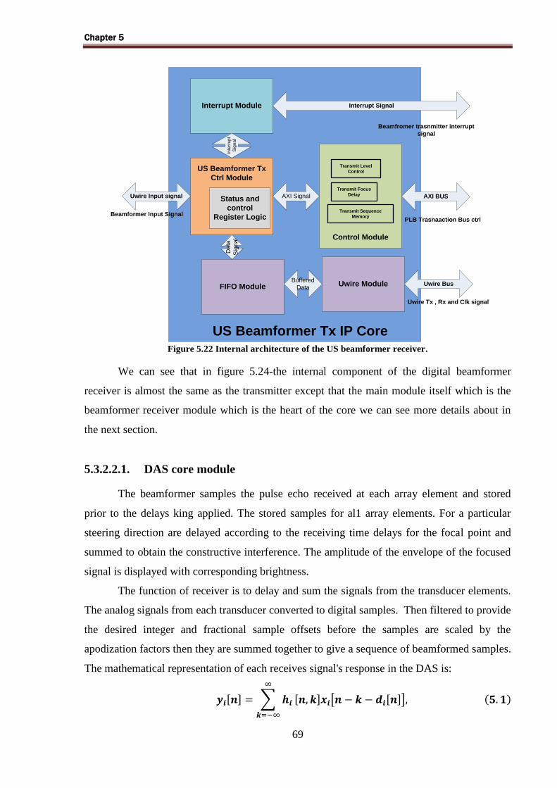
Chapter 5
69
Interrupt Module
Control Module
Uwire ModuleFIFO Module Uwire Bus
Uwire Tx , Rx and Clk signal
AXI BUS
Interrupt Signal
Uwire Input signal
US Beamformer Tx
Ctrl Module
Da
ta
Sig
na
l
AXI SignalStatus and
control
Register Logic
Inte
rru
pt
Sig
na
l
Buffered
Data
PLB Trasnaaction Bus ctrl
Beamfromer trasnmitter interrupt
signal
Beamformer Input Signal
US Beamformer Tx IP Core
Transmit Focus
Delay
Transmit Sequence
Memory
Transmit Level
Control
Figure 5.22 Internal architecture of the US beamformer receiver.
We can see that in figure 5.24-the internal component of the digital beamformer
receiver is almost the same as the transmitter except that the main module itself which is the
beamformer receiver module which is the heart of the core we can see more details about in
the next section.
5.3.2.2.1. DAS core module
The beamformer samples the pulse echo received at each array element and stored
prior to the delays king applied. The stored samples for al1 array elements. For a particular
steering direction are delayed according to the receiving time delays for the focal point and
summed to obtain the constructive interference. The amplitude of the envelope of the focused
signal is displayed with corresponding brightness.
The function of receiver is to delay and sum the signals from the transducer elements.
The analog signals from each transducer converted to digital samples. Then filtered to provide
the desired integer and fractional sample offsets before the samples are scaled by the
apodization factors then they are summed together to give a sequence of beamformed samples.
The mathematical representation of each receives signal's response in the DAS is:
, - ∑
, - [ , -] ( )

Chapter 5
70
Where yi[n] is the filtered receive signal for the channel at time sample n, hi [n, k] is
the coefficient of the channel interpolation filter at time sample n ,xi[n] is the receive signal
from the channel at time sample n ,di[n] is the integer delay for the receive signal from the
channel at time sample n .The DAS beamformer will be the reference design for this software
implementation [1,2]. After each channel of data is filtered, all of the filtered receive signals
are summed together as shown in equation 5.2:
, - ∑
, - ( )
Where y [n] is the beamformed signal at time sample n, M is the number of data channels. The
basic block diagram for time domain beamforming, shown for a sonar system, is provided as
Fig. 5.23. The top portion of the figure is common to both the time and frequency domain
beamformers. The output of this portion of the figure, labeled “X”, then provides the input
into the next stage of the beamformer, “X” for the time domain.
Figure 5.23- Basic methods of time domain beamforming for passive (and active) systems [4].
We will take TI software development kit as our reference in the development and we
will extract all the information related to the interpolation filter and their tested data to verify
our design. The previous equation should be transformed into logic design so we can
implement it in the FPGA.so in the digital design view we can look it as IP core which will be
attached to the AXI bus of the MicroBlaze. In principle Beamformer Receiver core
comprising the following parts:
Manager Unit
Delayed Data Filter
Interpolation filter
Apodization gain generator
Summation

Chapter 5
71
We will describe each component in brief in the next sections
5.3.2.2.1.1. Manager Module
The Manager Module controls the flow of data through the entire beamformer.
Although it operates on each channel, it is instantiated in hardware as a global module,
meaning there is only a single module that interfaces with each of the individual channel
processing hardware. This module contains a store of all of the information about the data
points required for beamforming. It tracks the time elapsed since transmission, and sends out
requests for beamformed pixels when appropriate. It also contains and distributes interpolation
and apodization values required for each pixel. By maintaining a central storage area for all
beamforming related data and releasing this data as a unit, timing difficulties are greatly
reduced. It is important to note that although each channel on the beamformer operates
independently, in order to simplify timing, they all operate synchronously on data items. This
means that a data point will only be requested to be beamformed by the Control Store when
the region is in memory on all of the channels in the FPGA. The address store can also stall
beamforming across the entire chip if this condition ever fails. In practice this means that
spacing imaging lines far apart will result in long periods of stall between processing of lines,
while spacing lines close together will make it impossible for the beamformer to keep up with
the input data stream. In either case, the beamformer will operate correctly.
5.3.2.2.1.2. Interpolation
The interpolation function is integrated into the data buffer. Linear interpolation can be
implemented as a FIR filter with two coefficients h [0] = 1−Dandh [1] = D. This is the same as
a 1.order Lagrange filter. The higher the order of the filter the closer it gets to the ideal sinc
filter. The formula for generating the coefficients for an nth order Lagrange filter is
, - ∏
( )
( ) ∏
( )
Figure 2.8 shows the results from the filter-test program for Lagrange filters of order 1,2,3,4
and 5. One thing to point out is that the filters of even order, i.e. 2nd and 4th order, seems to
perform better than the odd ordered filters. Figure 2.9 shows that magnitude and phase
response of Lagrange filters with delay=0.5 samples.

Chapter 5
72
Figure5.24 Signal-to-Noise ratio using Lagrange filters[22].
The even-ordered filters, i.e. those with length L=3 and 5, have a poor phase delay
response but a better magnitude response. The reason why the poor phase response does not
affect the filter-test result is connected to the fact that the delays are evenly distributed
between 0 and 1, causing an equal amount of phase shift in both directions. Indeed, when
delays are limited to the range between 0 and 0.5 there is no difference in the test-results for
even and odd length Lagrange filters. How the filter’s phase response affects the image quality
of an actual ultrasound image is still unclear.
5.3.2.2.1.2.1. Generation of the filter coefficient
We generate the filter coeffiecient depending on many parameters which are the
number of the filter coefficient tab , coeficcent order and the fractional delay , below down
there is our C routine for generate the filter coefficent :
for(filterCnt=0;filterCnt<numIntFilters;filterCnt++) { uint_least8_t n; int_least32_t D = filterCnt * fracDelay; // compute the numerator coefficients for(n=0;n<numNumFilterCoeffs;n++) { uint_least8_t k; int_least32_th_n = 1 <<numFilterCoeffs_qFmt; for(k=0;k<numNumFilterCoeffs;k++) { if(k != n) {

Chapter 5
73
uint_least8_tqFmt = 0; int_least32_tsf_num = D - (k <<fracDelay_qFmt); int_least32_tsf_den = n-k; int_least32_tsf; uint_least32_tnumPnts = 1; math_div_cor_32b_32b(&sf_num,&sf_den,numPnts,qFmt,&sf); h_n *= sf; h_n>>= fracDelay_qFmt; } } // end of k for loop // store filter coefficients in reverse order pIntFilters[filterCnt].pNumCoeffs[numNumFilterCoeffs-1-n] = (int_least16_t)h_n; } // end of n for loop // store numerator parameters pIntFilters[filterCnt].numNumCoeffs = numNumFilterCoeffs; pIntFilters[filterCnt].numCoeffs_qFmt = numFilterCoeffs_qFmt; // store denominator parameters pIntFilters[filterCnt].numDenCoeffs = numDenFilterCoeffs; pIntFilters[filterCnt].denCoeffs_qFmt = denFilterCoeffs_qFmt;
} // end of intFilterCnt for loop
5.3.2.2.1.2.2. Interpolation Filter Placement
The optimum placement of the interpolation filter also is an important consideration.
The filter can be placed either before delaying the receive signals or after they are delayed and
summed.
Figure 5.25-showing generation of the filter coefficient[21].

Chapter 5
74
5.3.2.2.1.3. Apodization
Applying an apodization function to the received signals can improve the quality of
beamformed images by reducing side lobe levels in the radiation pattern of the array.
Apodization reduces the amplitude of the received signals based on their location on the array.
We are using hanning window for generating our FIR filter coefficient:
Figure 5.26- showing hanning window for generating our FIR filter coefficient.
5.3.2.2.1.3.1. Generation of the apodization values
Generation of the apodization values using hanning algorithm need 3 parameters which
are number of samples, number of iterations and the selected active transducer. Generation of
the apodization routine is shown in the next c code.
int_least16_ttwoPi = TWO_PI_16B; uint_least8_ttwoPi_qFmt = TWO_PI_16B_QFMT; uint_least8_tnumIterations = 20; if(apodGain_qFmt<twoPi_qFmt) {
twoPi>>= (twoPi_qFmt - apodGain_qFmt); } for(sampleCnt=0;sampleCnt<numOutputSamples;sampleCnt++) {
uint_least16_tcnt = 1;
for(channelCnt=startChannelNumber;channelCnt<=stopChannelNumber;channelCnt++) {
int_least32_tnum = twoPi * cnt; int_least32_t den = numActiveChannels + 1; uint_least32_tnumPnts = 1; uint_least32_t index = channelCnt*numOutputSamples + sampleCnt; int_least16_tcosTh; int_least32_tth;
// compute angle math_div_cor_32b_32b(&num,&den,numPnts,0,&th);

Chapter 5
75
// compute the cosine math_cos_cor_16b_16b((int_least16_t *)&th,numPnts,numIterations,twoPi_qFmt,apodGain_qFmt,&cosTh); // store the value pApodGains[index] = ((1 <<apodGain_qFmt) - cosTh) >> 1; // increment the counter cnt++; } // end of elemCnt for loop
} // end of sampleCnt for loop break;
} // end of ApodGainType_Hanning case
5.3.2.2.1.4. Delaying
The method by which a linear array may be excited in order for the wavefront to
propagate in any desired azimuth angle is shown in Figure 5.27.
Figure 5.27- shows the coordinate system used to determine the time delay[19]
Needed for an element so that the summing of echoes from a target at a range and
angle produceconstructive interference. For the calculation, it is assumed that the echo
wavefront returning from a point scattered is of circular shape. The resultant delay , required
at an element that is at a distance x, from the center of the array for the delayed element's
output to coincide in time with the center element output is given by[21]:
{ ,
- ⁄ } , - ( )
Here is the radial distance from the array center and is the pointing angle relative
to the array normal. The constant c is the velocity of sound in the medium. Two problems
arise with the use of above equation in computing channel delay element times. First, the time
delay becomes negative and therefore non-causal for negative steering angles i.e. to the left of

Chapter 5
76
the center array. This can be overcome by adding a positive constant to the delays for all
elements. Second is the inseparability of and dependencies, Which make the direct
computation of the time delays time consuming. This can be overcome by the use of parabolic
approximation. Equation 6.1 can be approximated as[21].
{
} , - ( )
5.3.2.2.1.5. Delay filter coefficient Generation
As we described in the previous section Delay filter coefficient is a function of steering
angles and the radial distance we can see in the next c routine how we can generate the delay
filter coefficient.
for(channelCnt=startChannelNumber;channelCnt<=stopChannelNumber;channelCnt++) { // compute the radicand for the delay computation rxBf_genRadValues(pRxBfParams,channelCnt,pRadValues); // take the square root of the radicand math_sqrt_cor_64b_32b(pRadValues,numOutputSamples,32,relSqrt_qFmt,pSqrtValues); // compute the relative delay values rxBf_genRelDelayValues(pRxBfParams,channelCnt,pSqrtValues); } // end of channelCnt for loop
In this design, the total receive delay time in each receive channel is calculated and stored in a
matrix array for each scan, representing a single b-mode scan.
5.3.2.2.1.6. Summation
The role of the adder module in the beamformer is to combine the outputs from each of
the beamformer channels, and add them together with the output from the previous card in the
chain. Since each card will be processing data independently, the summation of data between
cards must be buffered such that it can be properly aligned, independent of the arrival of the
data terms. This is accomplished by using two FIFO buffers within the Adder module. One
FIFO Captures data passed from the previous card, while the second contains the summation
of the data from the current card. Due to bandwidth limitations, the tracking of individual
samples is not performed. Instead, with each transmit pulse all of the internal buffers are
cleared. The module then relies upon processing order to align values between processing
boards. The second stage of the adder module waits for both of these FIFOs to contain data

Chapter 5
77
before pulling terms out of them, adding them, and passing them down the backplane chain as
shown in the next Figure.
Figure 5.28 - Adder module functional diagram. Each beamformed data term is added to all others on the
card, and then stored in a FIFO buffer. Data from the previous card is alsostored in a FIFO. When both
buffers are ready, the terms are summed together, and passedown the chain.
5.4. Challenges and Limitations
Many challenges were faced and solved in developing the beamformer HDL code. Most
of these involved overcoming the limitations the hardware, such as removing speed
bottlenecks, memory high speed buffering requirements, and reducing the need to use
advanced mathematics. Although nearly any function could be coded, the added complexity
may not be justified by the end results. Each of the final three tasks have varying degrees of
mathematical complexity, and therefore the best place to perform these tasks needs to be
considered. Using VIVADO High level synthesis tool was the edge of our design as it
improve the dramatically the rate of our development due to overcoming the limitations the
hardware of removing speed bottlenecks, memory high speed buffering requirements, and
converting the advanced mathematics written in traditional C language into HDL language
with all the degree of the optimization.
5.5. Summery
Here in this chapter we describe in details the architecture of the ultrasound digital
beamformer, we go through all the firmware components and the system interfaces. The main

Chapter 5
78
components is the FPGA we start the design with VIRTEX 6 but we could utilize the low
price SPARTAN 6 for our system we discuss the main components in the FPGA and the
meaning of CLB, LUT and BRAM also we introduce the MicroBlaze softprocessor as the
house keeper for our system and its significant role in reducing the logic complexity. Also we
introduce the Uwire interface which is the beamformer interface and also we give
demonstration about this IP core and its components, also the deserializer using LVDS
interface the ultrasound receiver interface also we describe in details the main components of
the digital beamformer IP interface and its synchronizing and buffering techniques. We also
illustrated ways of optimization techniques in the interpolation and the summation which
being described in details in the next chapter. Also we give demonstration about the DDR
memory core being used and the Ethernet.

Chapter 6
79
Chapter 6
Ultrasound Digital Beamformer Implementation
6.1. Introduction
This chapter describes the methods and procedures for investigating experimentally the
proposed implementations of the digital beamformation. Moreover there is complete section
for describing the optimization done for the design. The hardware and software procedures of
each of all the design components are described below. Ultrasound images and testing vectors
are obtained from TI ultrasound development Kit. It includes the raw scan lined and the
parameters by which the scanning has occurred .
6.2. System Parameters
This section presents the various design parameters like beam angle that decides the
aperture length, temporal and spatial sampling periods, filter cut-off frequencies, and
attenuation coefficients. We can find below a summery for each parameter with its default
value which we are using in our testing as shown in table 6-1
Unit Value Description Parameter
Samples/u
m
4357718 sampling rate divided by the speed of sound FsOverC_samplesPerUm
26 power of 2 used to scale up the sampling rate
divided by the speed of sound
FsOverC_samplesPerUm_qF
mt
Line 1 scan line number Scan Line Number
M,Rad 13422 scan line spacing of the beamformer Scan Line Spacing
24 power of 2 used to scale up the scan line spacing Scan Line Spacing _ qFmt
um 0 the current spatial position of the beamformer Current Pos_um
0 the power of 2 used to scale the current spatial
position of the beamformer
CurrentPos_um_qFmt
rad 0 Current angular position of the beamformer CurrentAng
15 Power of 2 used to scale the current angular
position of the beamformer
CurrentAng_qFmt
Sample 2536 Number of samples per beamformer iteration Num Input Samples
Sample 128 Number of output samples per beamformer
iteration
Num Output Samples
1200 The maximum lead delay value Max Lead Delay

Chapter 6
80
1200 The maximum lag delay value Max Lag Delay
50 The number of scan lines Num Scan Lines
1 The number of multiple line acquisitions for the
beamformer
NumMlas
Channel 192 the number of transducer data channels in the x
direction
Num Channels
Channel 64 the number of active channels in the x direction Num Active Channels
3277 the fractional delay of the interpolation factors Frac Delay
15 power of 2 used to scale up the fractional delay
of the interpolation factors
fracDelay_qFmt
Int Filter
Type_
Lagrange
The interpolation filter type Int Filter Type
filter 8 the number of interpolation filters NumInt Filters
14 the power of 2 used to scale up the interpolation
filter coefficients
IntFilterCoeffs _qFmt
um 192 the number of transducer elements in the x
direction
Num Elements
um 501760 The transducer element spacing in the x
direction
Elem Spacing _um
10 the power of 2 used to scale up the element
spacing value in the x direction
Elem Spacing _um_qFmt
Transducer
Type _Linear
the transducer type Tr Type
Hanning
the apodization gain type Apod Gain Type
15 the power of 2 used to scale up the apodization
gains
Apod Gain _qFmt
Table 6.1 Beamformer receiver configuration parameters default values
In general this testing, a 192 element transducers only 64 element of them are active in
the receiving the echoes with a center frequency of 5 MHz is used. From the previous
calculation we get that that the signal from a 5MHz transducer would be too small to be
detected at 17.1cm of depth and having determined the maximum depth possible, we can then
use this to determine the maximum round trip time of flight (speed of sound in the medium is
approximately the same as water (1510 m/s) .Using this speed we can estimate the time

Chapter 6
81
required for a signal to penetrate to its maximum depth and return, it would require
approximately 0.22ms (0.171m*2/1510m/s) to complete the trip. By taking the reciprocal of
this time-of-flight, we can determine another key limiting factor for any ultrasound system:
the maximum number of pulses that can be completed per second. Again to continue our
example, this system could achieve 4415 pulses per second.
6.3. DAS Implementation
This implementation of digital beamformer is the earliest and commonly used
beamformer in commercial ultrasound imaging instruments. All the beamforming was done
after the data were acquired using the experimental imaging system. In this method, the
beamformer samples the pulse echo received at each array element and stored prior to the
delays being applied. The stored samples for al1 array elements. For a particular steering
direction are delayed according to the receiving time delays for the focal point and summed to
obtain the constructive interference. The amplitude of the envelope of the focused signal is
displayed with corresponding brightness.
6.3.1. DAS Image Formation
The Image formation is composed of three main stages which are rxBf_init () which
responsible for initialize the beamformer with the proper parameters for the beamforming
operations as well as generating the interpolation filter coefficient, the second is rxBf _setup ()
which is responsible for starting the parameters for the specific new scan line and the third
module which is rxBf _run () this function is beamforming itself it makes the calculation and
filtering to result beamformed data.
6.3.2. Beamformer Initializing Module
Beamformer initialization module is being used only one time at the start of the
beamforming process for certain object , it is responsible for starting the operation from new
scan line with the desired parameter for the specific region . A simple flow chart for this
process is shown in figure 6.1.

Chapter 6
82
/*generate the sine table*/rxBf_genSinTh(trType,
scanLineSpacing, scanLineSpacing_qFmt,
numScanLines, sinTh_qFmt,
pRxBfParams->pSinTh, pRxBfParams->pScratchPad)
/*initialize the filters*/rxBf_genIntFilters(intFilterType,
numIntFilters, numIntFilterCoeffs,
intFilterCoeffs_qFmt, 0, 0,
fracDelay, fracDelay_qFmt,
pRxBfParams->pIntFilters)
/*initialize the sample count*/gSampleCnt = 0
return
end
start(rxBf_init)
Figure 6.1-Shows the simple flow chart for the beamforming initialization module.
As shown in figure 6.1 there are 3 processes in the beamformer initialization module
which are:
Initialize the sin table of the steering angles (in case of phased transducer)
Initialize the interpolation filter coefficient
Initializing sample count
6.3.3. Beamformer Setup Module
This module is responsible for starting the operation from new scan line each scan line we
need to do the following procedures:
Reset the sample counter again.
Generate the start and stop channel indices.
Generate the apodization gain factor.

Chapter 6
83
Generate the initial delays.
Generate the compressed delay.
Generate the Interpolation coefficient
As shown in Figure 6.2, resetting the sample counter then we generate the start and stop
channel indices of the current firing and receiving according to the configuration parameters
and depending on type of the ultrasound transducer type, then we generate the apodization
gain then the compressed delay generation finally the initial delays generation
rxBf_setup
rxBf_resetSampleCnt
rxBf_genChannelIndices
rxBf_genApodGains
rxBf_genTd
rxBf_genDelayValues
rxBf_genCompDelayValues
math_div_cor_32b_32b
rxBf_genRadValues
math_sqrt_cor_64b_32b
rxBf_genRelDelayValues
main
// reset the sample count
// generate the start and stop channel indices
// generate the Appodization gain factors for the second line
//generate the initial delays
//generate the delay values
// generate the compressed delay values
Figure 6.2-Beamformer setting up flow.
6.3.4. Beamformer Running Module
In this experimental investigation the total receive delay time in each receive channel is
calculated and stored in a matrix array for each scan, representing a single b-mode scan. After
al1 the received information has been suitably delayed, the outputs are then summed. The sum
is then rectified, envelope detected and processed to obtain the brightness information. In case
of multiple receive zones, the delays for each channel. Focal zone and B-mode scan are stored
in a 3-dimensional array. The received information is first delayed for a range Rfpl along the
same azimuthal orientation. Once all the echoes within that focal region associated with Rfpl
are delayed. The delay in each of the channels is altered to produce a new focus some distance

Chapter 6
84
beyond the first. This process continues until al1 echoes from the most distant focal region
Rfpn have been delayed. This delay process is continued for each scan direction. For the DSA
architecture, a high sampling rate is required, however, if temporal interpolation of the receive
data is performed in conjunction with the beamforming operation, the received data needs
only to be sampled at the Nyquist rate. This is called interpolation beamforming. The
interpolation is accomplished by zero padding the original sequence, and passing the resulting
sequence through a finite impulse response (FR) low pass digital filter. For single scan line in
the running module we can summarize it by the following processes:
Zero out the summed data buffer
Zero out the filtered data buffer
Summing the resulted data
Interpolating the data
Combining the filtered data
Updating the sample counter
These processes are shown in figure 6.3.
rxBf_run
rxBf_computeNumBytesForSummedData
rxBf_zeroMemory
rxBf_computeNumBytesForFilteredData
rxBf_sumData
rxBf_filterData
rxBf_combineData
rxBf_updateSampleCnt
alignNumBytesOn64BitBoundary
main
Figure 6.3- Beamformer running flow.
In the beamformer running module we can find that they are depending on each other
first we are summing out the data then we zeroing out the filtered data then summing the result
data then the interpolation stage and finally combining out the filter data .
1-Reinitialize the memory again for new
scan line processing
3-Applying interpolation filtering
4-Combine the final result in one vector
2-Apply apodization and summing the active
channel in one vector

Chapter 6
85
6.3.4.1. Summing data
This stage comprises the following processes:
Initialization of the apodization parameters
Getting the Delay value
Apply Apodization
Accumulate
Packing the result data
At the beginning of the apodization stage we should initialize it with the desired
parameters which being adjusted to fit this target of the scan line, the second step is to get the
delay valued generated in the beginning of the operation once we have both we can apply the
apodization filter and accumulate with the last result of the apodization and finally packing the
result into one vector.
6.3.4.2. Interpolation Filter
Interpolation filtering comprises the following 7 processes:
Interpolation Parameters Initialization
For each output sample and For each coefficient element doing the following procedures:
o Loading the filter coefficient
o Loading the input data values
o Apply the filter coefficient
o Packing the result data
o Scale the result
o storing the result
In the interpolation filter process we are using it to interpolate between each output
sample and for each of the interpolation coefficient we are generating the required interpolated
data and for each iteration we should load the filter coefficient, loading the input data from the
apodization stage then applying the interpolation filter then pack the result and scale it with
our maximum and finally storing the result data.
6.3.4.3. Combining the data
The combining of the beamformed data composed of two main steps:
Initializing the data
Combining the data

Chapter 6
86
For each output sample and for each coefficient
o Load the data
o Accumulate the data
o Round the data
o Scale the data
o Pack the result data
o Save the result
6.4. DAS Simulation and results
As we did not have a complete implementation for our proposed design , we choosed a
study made for system similar to our proposed firmware design (implemting almost the same
the DAS algorithm ) . this study has been made by Sunil Vasudevan [21] for studying the
differences between DAS and SAR DBF algorithms. He got Ultrasound images from a Aloka
ultrasound machine (Aloka, Tokyo, Japan, model: SSD-246), manufactured in 1944. The
transmit part of the system is a parallel real-time transmit system with a 3MHz, 64-element
linear transducer array and pitch of 2 mm. The elements are 0.2mm from the probe surface.
The transmit circuitry of the machine consists of a trigger which generates a gated square
pulse. The amplitude is variable from O to 400 V p-p. This tngger pulse is applied to the
transmit elements through a dual channel multiplexer.
6.4.1. Testing Phantoms
The RF data that are used for experimental investigations are acquired from different
phantoms. Since the receiving part of the experimental system described above is not real-
time, it excludes investigations where movement distortion could be a problem. Hence al1
imaging is done on custom built and standard phantoms. Phantoms used in this thesis for the
investigations rnay be classified into water phantoms and tissue-mimicking phantoms.
a) Lucite block in water bath
This phantom has a single Lucite slab of dimensions 12.5 x9 x 1.5 mm which is
imrnersed in a plastic tank holding de-mineralized and distilled water. Lucite is assumed to be
a perfect reflector. This phantom is used to characterize transmit and receive beam patterns of
the transducer array. The rf signals received are also used to set system parameters such as
signal bandwidth, center frequency of transmitted signal and filter cut off frequencies.

Chapter 6
87
b) Lucite block holding tubes of di fferent lengths.
A Lucite bIock of dimensions 12 x 6.5 x 4 mm has holes drilled on the surface to hold
hollow plastic tubes of 2 mm diameter. Copper wires are inserted ir? the hollow tubes to
increase the reflectivity. The lengths of the tubes Vary from Lmm to 8 mm. This phantom is
in a degassed water bath. It is used to find the point-spread function (PSF) of the different
methods.
C) Metallic sphere on Lucite slab.
This phantom has a metallic sphere of diameter 2.5 mm on a Lucite block of dimensions 12.5
x9 x 1.5 in a degassed water bath. This phantom is used to view improvements in edge
detection with bearn forrning.
d) Lesion and scattenng phantom.
This phantom is custom made (Ernest L. Madsen, Dept of Medical Physics, University
of Wisconsin, Madison). It has a number of spherical lesions of diameter 6 mm and a
backscatter coefficient 14 dB below their surrounding medium. The lesions have a
attenuation slope of 0.5 dB/cm/MHz. The surrounding medium consists of glas bead
scatterers of 45-53 microns in diameter range. There are 4 grams of beads per litre.. It is used
to compare over al1 image quality for different methods.
e) Cyst and Wire phantom
This is a wire and cyst tissue mimicking phantom (Nuclear Associates, model: #84-3
17). This phantom has a senes of monofilament nylon targets. 0.375mm in diarneter that are
separated over varying distances. It also has four simulated cysts of diameters 4, 6, 8 and
12mms.(cylinders of gel with no scattering). The filling medium is a hydrogel containing a
scattering agent that simulates human liver parenchyma. It is used for comparing the overall
image quality and finding the point-spread function.
6.4.2. Testing configuration
Configuration A simulated a single transmit focus and receive focus using 128
elements which were uniformly weighted. Configuration B simulated a conventional analog
beamformer with single transmit focus and multiple receive focal zones. Each zone had a
length of 20 mm. It used 64 active elements for transmit and Hanning apodization to weight

Chapter 6
88
the elernents (both transmit and receive). For configuration C. four transmit and receive focal
zones were used. The length of the focal zones was 20 mm. 128 transmit elements were used.
Configuration D simulated a typical digital beamformer, with multiple transmit focus and
dynamic receive focus. The transmit had four focal zones of length 20 mm. Hanning
apodization is employed to maintain a constant f-number over each focal zone. A f-number
of 4 was used on transmit and 2 on receive. For configuration A, a point target at the transmit
focus was used. For configuration B, C and D, a five point target with the points at the center
of each focal zone was used. These configurations represent the gradua1 evolution of
beamformer from analog to the present day digital beamformer
6.4.3. Testing Results
Figure 6.4 shows the point spread function (PSF) calculated at a focal range of 100 mm
using the configuration. The plots showed the spatial variation of beam width and side lobe
level without a) apodization, b) with rectangular apodization and c) with Hanning apodization,
as a function of the lateral and the axial distances.
Figure- 6.4 Images produced with single transmit and receive focus displayed over a 40 dB range. The data
are coilected fiom a wire object using configuration A with the object positioned at 100 mm: (a) wirhout
apodization, (b) rectangular apodization and (c) hanning apodization. All lateral and axial distances are in
milimeters[21].
To a large extent the performance of an ultrasound irnaging system is characterized by
the spatial response of the transducer. From the response, one can determine the spatial
resolution as well as the image dynamic range, the two most important parameters of image
quality. We see a decrease in beam width and side lobe level with apodization (Figures 6.4b
and 6.4c), thus indicating a improvement in image quality when compared to the image
without apodization (Figure 6.4a). The peaks of al1 the PSF's are normalized to one
corresponding to the maximum value of the main lobe. Table 6.1 shows the beam width
measured at -6 dB and the side lobe levels for each window versus the focal range.
a b c

Chapter 6
89
Table -6.2 Beam width and side lobe level Vs Focal range: (a) without apodization, (b)
rectangular apodization and (c) hanning apodization[21].
The values for beam width versus the focal range are plotted in Figure 6.5, indicating that apodization does help
in controlling the beam width as we move into the far zone. where the gradua1 divergence of beams occur.
Figure -6.5 Cornparison of 6-dB btamwidth versus focal range for a wirr object obtained using
configuration A[21].
Figure 6.6 shows the cornparison of the -6 dB beamwidth versus the depth for the linear amay
in configuration A. The point spread functions for the wire object are calculated at distance of
3 mm, 5 mm and 7 mm respectively from the fixed transmit focus of 100 mm. The numerical
values are tabulated in Table 6.2.
Figure 6.6 -Comparison of 6-dB btamwidth vasus dcpth for a wire object imaged using
configuration A[21].

Chapter 6
90
These results indicate that apodization does help in improving the spatial response, when the
objects appear beyond the focal region..
Table -6.3 Resolution of a wire target away from the focus of LOO mm for (a) without
apodization, (b) rectangular apodization and (c) hanning apodization[21].
Figure 6.7 shows the surface plots of a 6 wire phantom obtained from configurations B, C and
D. as described in Section 6.1, which shows the bearn responses and side lobes for the arrays
modeled. The surface plots are used to bring out the effect of various configurations on beam
response and sidelobes, that may not be visible in gray-scaled images due to the scan
conversion.
Figure 6.7-Surface plots of images of a six wire phantom obtained from (a) configuration B. (b)
configuration C and (c) configuration D[21].
The six wire objects areat distances 35, 50, 65, 80,95 and 1 10 milimeters. Figure 6.7a shows
the surface plot for configuration B, that had a fixed transmit focus at 60 mm and five receive
f~al zones starting at 10 mm from the array surface and with a zone length of 20 millimeters.
It uses 64 elements dunng transmit and al1 128 elements for receive. Figure 6.7b shows the
surface plot for configuration C that had four transmit points at 40, 60, 80 and 120 milimeters
and five receive focal zones with sarne parameters as configuration B. AI1 the 128 elements
are used for both transmit and receive. Figure 6.7c is the surface plot for configuration D
which employed dynamic apodization and dynamic receive that continousally 'tracked' the

Chapter 6
91
receive echoes. The system had four transmit points at 40, 60, 80 and 120 milimeters and the
data are sampled at a frequency of 25 MHz . These plots bring out the efficacy of a digital
bearn former in improving the image quality by Iimiting the beam spread and elminating side
lobes (Figure 6.7c), as compared to the other two configurations (Figures 6.7a and 6.7b).
Also the ability of the digital beamforrner to pick up signais in the far zone better than
configuration C with multiple focus, is evident frorn Figure 6.7c. In order to generate the
plots shown in Figure 6.8, a PSF is calculated at various ranges between 30 and 120 mm. The
lateral response on milimeters at -6 dB and -10 dB were computed for each PSF.
Bea
m w
idth
[m
m]
Beam Range [mm]
a)
Beam Range [mm]
Bea
m w
idth
[m
m]
b)
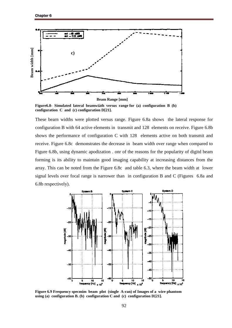
Chapter 6
92
Figure6.8- Simulated lateral beamwiàth versus range for (a) configuration B (b)
configuration C and (c) configuration D[21].
These bearn widths were plotted versus range. Figure 6.8a shows the lateral response for
configuration B with 64 active elements in transmit and 128 elements on receive. Figure 6.8b
shows the performance of configuration C with 128 elements active on both transmit and
receive. Figure 6.8c demonstrates the decrease in beam width over range when compared to
Figure 6.8b, using dynamic apodization . onr of the reasons for the popularity of digitd beam
forming is its ability to maintain good imaging capability at increasing distances from the
array. This can be noted from the Figure 6.8c and table 6.3, where the beam width at lower
signal levels over focal range is narrower than in configuration B and C (Figures 6.8a and
6.8b respectively).
Figure 6.9 Frequency specmim beam plot (single A-ran) of Images of a wire phantom
using (a) configuration B. (b) configuration C and (c) configuration D[21].
Bea
m w
idth
[m
m]
Beam Range [mm]
c)

Chapter 6
93
Table 6.3 presents the results that provide a comparison of the three configuration B, C and D
that are modeled. Figure 6.9 shows the lateral PSF's for the configurations B, C and D,
obtained for the wire phantom described above. The magnitude is in dB and is normalized to
the peak value. The PSF was calculated at range of 100 mm for each system. An increase in
overall signal level is consistent with the discussion (Section 3.2) on digital beam forming
(Figure 6.9c). when compared to analog bearnformers (Figure 6.9b and 6.9c)
Table -6.4 The percentage narrowing of the lateral resolution of system C and D
referenced to system B[21].
6.5. HDL Design Performance
The success of an HDL design can be measured in various ways. Commonly, design
performance is measured by maximum clock speeds achievable, while device utilization is a
measure of how well the design fits in the selected FPGA
6.5.1. HDL Clock performance
The clock speeds are determined by the slowest measured logic path combination in
any clock domain. Often times the design can be run faster than is indicated by these results
without noticeable effects since limiting paths may be non-critical, or only occasionally used.
However, these provide a baseline for performance. These results are also calculated at the
maximum (worst case) operating conditions of the devices, usually at 85 degrees Celsius, with
core voltage 5% (1.14V). Again this provides a worst case performance achievable that is
usually bettered in practice. Finally, if further performance gains are required, these results are
entirely dependent upon internal logic placement and routing, and higher effort levels (or
tailoring of design constraints) in the place and route engine may yield additional performance

Chapter 6
94
improvements. The timing results for the complete design calculates that the maximum clock
speed for the processing clock which determines the maximum beamforming speed, is
187MHz. In the current system this clock is only being run at 100MHz.
6.5.2. Device resources utilization & clock performance Tradeoff
FPGA utilization is how effectively and efficiently utilizes the internal resources of the
FPGA. Normal coding techniques and synthesis tools implement every logic to LUT based
architecture. Which utilizes more area on the chip and some fast and dedicated area of the chip
remain unutilized. Which in turn results in slow clock rates and bigger critical path lengths,
hence the design remains inefficient in terms of both speed and area. In this paper we will
present and discuss some techniques to effectively utilize the FPGA resources in order to
speed up the clock rates and reduce the area utilization. Although Device utilization is very
important factor in reducing power consumption as well as the cost, this is due Choosing
smallest package that fulfill design requirements have direct influence on the power
consumption and the cost of the design.
6.5.3. Digital Beamformer Utilization
The RTL synthesize is the next step after coding stage. In the synthesize stage first we
check the design flow diagram as shown in figure 6.10.
Figure 6.10- design viewer.
As shown in Figure 6.10 there is top level module which is rxbf_run_synth . This is the top
level module of the DAS digital beamformer algorithm and composed of three modules the
rxbf_sum_module , rxbf_filter_module and rxbf_combined_module.
6.5.3.1. Default RTL Synthesizing
In this default synthesize without any type of optimization we got a big latency of clock
(Worst case 190,000 cycles). The result of the synthesized design shown in figure 6.11.

Chapter 6
95
. Figure 6.11- design viewer of the optimized synthesized.
Also we can figure out the device resource utilization is not encouragement for replacing this
family with less FPGA , we can find DSP resources reached to 70% of the device without
adding the remaining modules.
6.1.1.1. Performance Optimization
To utilize the device more in the area of the performance by making the best use of the
parallelism of the FPGA. There are two important options in the VIVADO HLS to utilize the
parallelism of the RTL synthesize. These options are the pipelining and data flow behavior
of the code flow. In figure 6-12 the designer view shows the top level module which is
rxbf_run_synth embedded in the Dataflow option and the three modules the
rxbf_sum_module , rxbf_filter_module and rxbf_combined_module are inside the top level
function.
Figure 6.12 -design viewer after the performance optimization.
We can see the optimization results in figure 6.13 , in the performance estimate tape the
clock latency reached to 44,000 cycles this leads to 5 times faster than the default
synthesizing . Although we can find out increase in the resource usage in the BRAM_18K
(62% instead of 32%), FF (11% instead of 8%) and the LUT (34% instead of 24%).
Figure 6.13- showing Project Performance Optimization.

Chapter 6
96
6.5.4. FPGA VS DSP Performance
By measuring the DSP target performance (profiling result for performing digital
beamformer operation with Kernel Complexity equal C64x+TM CPU cycles, based on CPU
cycle accurate Simulator) we got result which is big than the proposed designed , the
comparing is made in the table 6.5
Module DSP FPGA
rxBf_sumData 85,134 34,753
rxBf_filterData 9,682 8,821
rxBf_combineData 3,861 646
Total operation 100,000 44,225
Table 6.5 Shows performance comparison between FSP & FPGA
This comparing is done using the following parameters:
the number of scan lines 1
number of interpolation filter coefficients 8
number of interpolation filters 10
number of receive data channels 64
number of output samples per iteration of the beamformer 128
Module DSP FPGA
rxBf_sumData 85,134 10,625
rxBf_filterData 9,682 8,801
rxBf_combineData 3,861 721
Total operation 100,000 20,150
6.6. HDL Verification and Test Benches
Large and complex HDL code designs can be extremely difficult to debug. The
approach taken with this project was to make extensive use of unit test modules to verify base
functionality, along with full scale simulations to test the completed design. Register Transfer
Level (RTL) code is simulated using an HDL synthesis package. For this project, the Xilinx
ISE Simulator was used. A screen shot of the interface is shown in Figure 5.7. In this Figure,

Chapter 6
97
modules are listed in the far left pane, selected signals to record are presented in the center,
and their resulting simulated waveforms are on the right we have two simulation here Figure
5.7 show Edge and phase detect diagram for RxClk (CLK0) before RxClkNot (CLK180) for
beamformer receiver and Figure 5.8 show Edge and phase detect diagram for RxClkNot
(CLK180) before RxClk (CLK0) for beamformer receiver.
Figure 6.14- Test bench for Edge and phase detect diagram for RxClk (CLK0) before RxClkNot for
beamformer receiver.

Chapter 6
98
Figure 6.15 Test bench for Edge and phase detect diagram for RxClkNot (CLK180) before RxClk (CLK0)
for beamformer receiver.
6.7. Software Simulation and Result Verification
In this section we are showing how we are simulating the digital beamformer receiver
operation and how can we verifying our result.
6.7.1. Testing Environment
In this verification section we are using Code composer studio to prove our digital
beamformer algorithm , code composer studio is integrated tool based on eclipse IDE.TI
integrate all their controllers (MSP430 , DSP ,…) in this tool here we are using C64x as
reference for our implementation. We can have a look in the code composer studio shown in
figure 6.16
Figure 6.16- Code composer studio view.
6.7.2. Testing Vectors and reference

Chapter 6
99
Figure 6.17- TI Testing & validation folder
Figure 6.17 shows many test cases reference result as shown in the left side and the
right side our result which is empty before running the beamforming simulation and
verification.
Figure 6.18-many test cases references for beamformer validation method
Figure 6.19- shows the content of the input folder with highlighting one test case
vectors which include Scan line vector, apodization gain parameter vector, compressed delay
vector, the filter parameters data vector and the generic parameters for this test case.
Figure 6.19-Content of the input folder.
6.7.3. VIVADO HLS Simulation and verification
For simulate the digital beamformer receiver we are simulating the hardware
environment by feeding the parameters vectors into code composer studio then running it and
out here in the next figure we will show the welcome message in the debugging.

Chapter 6
100
Figure 6.20-Testing welcome message.
In the debugging we are going into multiple of stages first of all beamformer parameters
initializing is the first step in the beamformer as shown in figure 6.21the initialization
parameters is loading these configuration parameters which described in table 6-1and this is
one vector of the input files.
Figure 6.21-Initializing the beamforming stage.

Chapter 6
101
The next step is the digital beamformer setting up in this stage we are start up the
digital beamformer with the parameters being loading from the last step as shown in figure
6.22.
Figure 6.22-Configuring the beamformer with the general parameters.
The next stage is to allocate memory for this testing by calculating the space for filter
coefficient vector, the apodization gain vector, compressing delays vector and scan line vector
as shown in Figure 6.23.
Figure 6.23-Allocating memory for different component of the beamforming.

Chapter 6
102
The fourth stage is to setting up the filter coefficient vector with the input file as shown in
Figure 6.24.
Figure 6.24-Loading interpolation filter coefficient.
All the previous configurations made for all the next scanning line but for each line we
should configure it with different apodization and delaying values. Here down we start each
scan line processing by applying apodization gain first. Figure 6.25 showing the while loop for
the beamforming processing for each scanning line.
Figure 6.25-Configuring the apodization gain for each of scanning line.

Chapter 6
103
The second stage for processing the scanning line is setting the compressed delay
vector from the input folder this stage is shown in Figure 6.26.
Figure 6.26-Configuring the delay values for each scan line.
The third stage for the scan line beamformer processing is the getting the input vector
from the input folder as shown in Figure 6.27
Figure 6.27-Reading the raw scan line vector from TI input folder.

Chapter 6
104
Finally the last stage in the processing is running the beamforming after the proper
configuration for the entire beamforming component as shown in figure 6.28.
Figure 6.28- Running the beamformer operation on the selected scanning line.
After finishing the operation for the scanning line we stored the output of the result in the
output folder for comparing as shown in Figure 6.29.
Figure 6.29-Writing the result output vector into file for comparing.
While the beamforming operation we are logging these events in the console output
view we can see the logging events in figure 6.30.

Chapter 6
105
Figure 6.30-Beamformer logging view
Now after finishing all the testing we can have a look for the beyond compare view as shown
in Figure 6.31 and 6.32.
Figure 6.31-Shows all the beamformer where successfully output the exact as the Ref.
Figure 6.32 -Comparing the reference with the result for single test case vector

Chapter 6
106
6.8. Implementation Summary
In this chapter we describe the digital beamformer Firmware implementation using a well-
defined US development KIT from TI; it includes a reach library of test vector from which we
could verify our development against its reference vectors. Moreover our design of the digital
beamformer framework referenced from the TI US development kit developed and testing using
VIVADO HLS IDE. We succeeded in utilizing the VIVADO HLS in developing our receiver
digital beamformer to produce it in a ready- made IP core working in EDK. We succeeded in
the optimization phase of the IP core. We decreased the complete design of the beamformer
from latency of 400,000 cycle (11 nsec) to 41,000cycles (nine nsec) against 100,000 cycles (one
nsec) of the TI C64X DSP for 64 channel operation. This means we could achieve (1/3) of the
DSP processing for the 64 channel processing (almost the same processing time for our target at
16 channel beamforming processing). Moreover in the testing result the efficacy of the
proposed Delay-Sum-Add architecture is compared with the common analog beamformer
architecture. The images generated using the analog beamforming (Aloka, SSD-246) show poor
lateral resolution because of the transducer array design of the ultrasound machine used. The
DAS method does improve the image quality and lateral resolution. Properly delaying the
samples and summing them, produces a coherent, strong signal with a narrow beam width and
lower side lobes.

Chapter 7
107
Chapter 7
DBF Discussion and DAS Limitations
7.1. Discussion
Images have significant improvement in lateral resolution after apodization when
compared with images produced with no apodization. The processed images show better
resolution and lower side lobe level compared to unprocessed raw data. These figures show
gray scale images of a typical wire object created using configuration A. The unprocessed
image (without apodization) has wide lateral resolution due to the spreading of the beam. The
other processed images which produced after processing exhibit progressively narrower lateral
resolution, even though the differences between the rectangular apodization and hanning
apodization cannot be distinguished easily from these figures. Apodization weights the
elements to the produce apertures, these apertures restrict the spread of the beam, thus produce
narrower beams when compared to cases without apodization. The weighting also reduces the
side lobe level resulting in an increase in dynamic range, where dynamic range is the ratio of
maximum axial response to the maximum off-axis response. By comparing the previous
results we found that images with no processing done on the RF data has wide beam at the
focus and also higher sidelobe levels, on the other hand on the processed images the beam is
narrower and also produces lower side lobes (hanning apodization produces lower side lobes
and narrower beams when compared to a uniform rectangular apodization). The improvements
in the sidelobe level results from the product of the apodized transmit beam pattern and
receive beam pattern. It can be observed from Table-6.1 that the side lobe levels are around -
10 dB when there is no processing and around -1 i dB and -15 dB with uniform apodization
and hanning apodization respectively. Also the side lobe levels after processing are
progressively lower levels as the focal range increases. The reduction in side lobe level
amplitude for hanning windows increases larger ranges, when compared with rectangular
apodization. This can be attenuated to the non-uniform nature of weighting. The results
obtained are expected as discussed on in Section 4.2, except at 103 mm for rectangular
window, which shows a higher level than the non-processed case. This may be due to errors
(inaccurate measurements) in the simulations conducted. Figure 6.5 shows the improvement
in beam width as a function of focal range with apodization. Although lateral resolution
should be independent of depth, the resolution of the wire at 107 mm with rectangular
apodization is worse than the two wires at shallower depths. In case of hanning apodization it

Chapter 7
108
can be noticed that, the resolution remains almost constant with increasing depth. In case of
resolution without apodization, there is a marked increase in the beam width as we move from
the array. This is due to the broadening of the beam in the far zone, while in processed cases
weighting controls the beam width. Figure 6.6 shows the lateral beam width versus depth.
There is a gradual deterioration in the lateral resolution as the object is placed at increasing
distances away from the fixed focus. This is expected, but as cm be observed from the plots,
the deterioration in the lateral resolution is far less when apodization is used and hence
increase focusing. These beam widths are compared to the beam widths at the focus for both
processed and unprocessed cases, which are found to be 3.1. 3.3, 3.7 millimeters without
apodization, with rectangular apodization and with hanning apodization respectively. A
hanning window has a gradually decreasing slope compared to the rectangular weighting.
From Figure 2.4 (Section 2), it can be noted that the hanning window approaches zero in
smoother fashion and hence contributes to better beam width control. Figure 6.7 is the surface
plot comparison for a typical simulated analog beamformer with single fixed focus and
multiple transmit focus and a digital beamformer with dynamic apodization and receive. The
analog beamformer with single transmit focus (configuration B) show higher beam spread and
side lobes around the deeper wire objects. The analog beam former is focused at one point on
transmit and hence there is a gradual convergence of the beam around that focal point only,
resulting good resolution at the focal point. Using a multiple transmit foci and receive method
(configuration C) improves the axial and lateral resolution (Figure 6.8c). The beam widths are
narrower when compared to configurations B and D due to the use of a larger aperture.
However this causes an increase in number of side lobes. Figure 6.8 shows the remarkable
improvement achievable by employing a digital beamformer. The sides lobes are practically
non-existent, which is due to the continuing focus maintained on receive. The beams show
better focusing because of dynamic apodization, where the ratio of the aperture to the desired
focal depth are greater than the ratio of array length to its focal length. Figure 6.8 plots the
beam width versus the focal range at two signal levels. The advantages of using a digital
beamformer are obvious. The lateral resolution deterioration at lower signal levels is higher in
configurations B and C than in D. The beam widths are double when compared at the -6 dB
level. The depth of field is significantly reduced when a single transmit focus is used. There is
an increase in beam width see from Figures 6.8a to 6.8c of approximately 100% at -6 dB.
Configuration C and D show narrowing of the beam at -10 dB for deeper distances. This is
due to the use of multiple transmit and receive. At the -6 dB signal level, the beam width for
configuration B increases dramatically beyond the fixed transmit focus while in configuration

Chapter 7
109
C and D, they are nearly constant for the entire focal range except at later depths. The
diffraction limited resolution at al1 ranges is because of the transmitting and receiving
aperture are nearly in focus- However configuration D requires a complex scan converter and
a large dynamic range for the ADC's. The beam width for configuration C is lower than for
configuration D for all ranges, is due to the use of a larger receive aperture. Figure 6.9 shows
the frequency spectrum for each system. Configuration D has lower side lobe levels around -
25 dB. This is due to the dynamic apodization. Configuration C shows higher side lobe levels
around -20 dB, which is due to the larger aperture king employed. Configuration B shows
higher side lobe levels due to the lack of any control on transmit for deeper distances. Table
6.3 shows that there is an improvement in lateral resolution of about 50 % for configuration D
when compared with B for al1 ranges. There is nearly a 30 % increase in lateral resolution for
configuration C when compared with B but it is better at higher signal levels
7.2. DAS Algorithm Limitation
There are certain limitations associated with the Delay-Sum-Add architecture. These
limitations are:
1) target ambiguity caused by ohase quantization errors
2) limitations in delay line systems
3) increased hardware complexity
4) low frame rate
The time delays for transmit and receive are usually discrete. This leads to quantization
approximation to the ideal focusing and steering delay curves. This in tum can lead to a phase
grating effect that produces grating lobes within the image field of view. These are
independent of the amplitude grating lobes produced to due to the inter-element spacing.
Several approaches have been considered to minimize the grating lobes, one of the solutions
king decreasing the time delay increments. Even though the digital delay systems have
become practical and offer many advantages over analog delay lines, there are shortcomings
primarily associated with sampling rate and noise in the digital circuitry. Since the sample rate
is generally four to ten times to that established by the Nyquist criterion, the minimum delay
increment is larger thus causing phase quantization error and also necessitates the use of A/D
converters with large dynamic range, increasing the cost of the beamformer. This limitation
can be avoided with use of interpolation beamforming as discussed above. The system
complexity is directly related to the number of elements or channels in an array that is used for

Chapter 7
110
transmit and receive. In DSA architecture since al1 the elements are used for transmit and
receive, it increases the hardware needed for each channel i.e. each element would need a
delay line, ADC, amplifier etc. All this increases the cost of the system. Reducing the number
of active elements by employing synthetic aperture methods can reduce the system complexity
and cost which is discussed next. The use of a large number of elements increases the number
of beam lines which means better resolution but a slower frame rate. Thus DSA architecture is
not suited for high speed imaging like 3-D ultrasound imaging.
7.2.1. Synthetic Aperture Imaging Architecture
The architecture for digital beamforming with synthetic apertures is described in
section as well as the proposed designed for such system. The synthetic approaches can be
separated into two classes:
A. Synthetic receive apertures
B. synthetic transmit or transmit / receive aperture
With synthetic aperture processing, the goal here is to achieve a level of performance
without actually employing all the transmitting and the receiving channels. The approach used
involves transmitting with two or more transmit sub apertures and receiving with two or more
sub-arrays. Though this approach has received much attention in the literature, few if any
results of practical applications have been reported. The approach used here uses partial beam
sums that are obtained from signal subsets of overlapping receive sub apertures on consecutive
firings. This architecture is called multi-element synthetic aperture focusing method (MSAF)
[80]. The MSAF system is shown in Figure 7.1 with a five element active transmit (Kt = 5)
and five element active (Kr = 5) subapertures.
Figure 7.1 -MSAF system with a five element active transmit (Kt = 5) and five element active (Kr = 5)
subapertures [80]

Chapter 8
111
Chapter 8
Conclusion and Future Work
8.1. Review of Work Completed
This thesis has presented the work done designing, building, and testing a versatile
ultrasound beamformer system. We Proposed a design based on the DAS digital beamforming
implementation, it is consists of a 16 channel signal processing board. The modular nature of
the design allows the hardware to expand to the size needed by any front-end transducer, from
the largest 2D arrays, to the smallest annular devices. Even with this expansion, the on-board
power distribution, and self-contained processing hardware ensures that every channel will be
as robust as every other. The allocation of an expandable on board RAM further extends the
usefulness of the hardware for research. For all of these advantages, the hardware is small,
efficiently designed, and leverages the best of consumer electronics in order to minimize the
actual system cost. The total expected cost per channel is between $25 and $40 The HDL
firmware that has been created for the signal processing card is extremely optimized using
VIVADO HLS at processing ultrasound data. Limited RAM resources are over comed using
DDRAM. High-speed 387MHz DDR inputs are reliably deserialized using a dynamic phase
alignment on the. Both the programming framework used, and the availability of CPU
resources allow the software to be extended to perform additional real-time signal processing
Taken as a whole, the beamformer system is fast, robust, versatile, cost-effective, and easy to
use. All tests performed on individual component of it, have shown that desired performance
has been met or exceeded. In usage, the design has consistently exceeded design requirements,
all while costing a fraction of commercial options. All tests indicate the current system is
ready to be used in real-time 2D imaging, with up to 64 Active elements per scanning. This
design will provide an ideal platform for development, into the foreseeable future.
8.2. Future development ideas
The future development plane can be divided depend on the execution time, we can be
divided our plan into two terms: Long term Future Work and Short term Future Work. Both
will be discussed in details in the following sections.

Chapter 8
112
8.2.1. Short-Term Future development
The short term development plan is based on enhancing & optimizing the current and
it is divided into four areas where we believe opportunities exist to further improve the
system. First thing we need to complete the digital Beamformer configurability using the
standardized backplane idea, actually we did the PCI interface in the signal processing board
but we need to design the backplane board itself we need to continue work in the completing
designing the PCI commands, defining the rules and the actions of the backplane system i.e.
our card is one unit and we can add more cards to make 32, 48 … digital Beamformer with big
number of active transducers. The second this we need is to develop GUI software on the
desktop PC to manage the user parameters also it can be used for adding/removing certain
digital Beamformer cards to extend/shrink the system channels ,This software is controlling
our boards using the Ethernet or the PCI interface. The third thing is the Ethernet design is the
network port for accessing multiple Beamformer from remotely device, already we did the
interface implementation but we did not finish the application itself. This integration would be
the final step in producing a completely self-contained reconfigurable ultrasound beamformer
system. The existing buses would work just as well for the transmit electronics, and the
Ethernet Port card would serve as a break in the high-speed backplane ports, between a
downstream receive bus, and an upstream transmit bus, without any changes in the backplane
itself. Finally the Image compression need to be implementing to increase the processing
speed as it would allow for completely arbitrary image formation. Additionally, selecting an
efficient algorithm that relies on more computational logic and less storage would balance the
hardware resource usage better; this could possibly lead to an increase in processing speed and
allow the use of a smaller FPGA device to further save on cost
8.2.2. Long-Term Future development
The Long term plane is the development of the 3D digital beamforming .Due to high
processing operation required for this type of development an alternate implementation of the
digital beamforming (SAR) will be utilized for the next future plane.
8.2.2.1. Proposed design of the SAR
Svetoslav Ivanov Nikolov describes a design and implementation of a real-time delay-
and-sum synthetic aperture beamformer [81]. The beamforming delays and apodization
coefficients are described parametrically. The image is viewed as a set of independent lines

Chapter 8
113
that are defined in 3-D by their origin, direction, and inter-sample distance. The delay
calculation is recursive and inspired by the coordinate rotation digital computer (CORDIC)
algorithm. Only 3 parameters per channel and line are needed for their generation. The
calculation of apodization coefficients is based on a piece-wise linear approximation [82]. The
implementation of the beamformer is optimized with respect to the architecture of a novel
synthetic aperture real-time ultrasound scanner (SARUS), in which 4 channels are processed
by the same set of field-programmable gate arrays (FPGA) as shown in Figure 8.1.
Figure [8.1] - Overview of the beamformer is architecture. The beamformer is divided into blocks.
Each block creates a part of a high-resolution SA image using data from 4 receive channels. Data are sent
further in the system after all transmissions have been carried out [83].
This design is modular, and a single beamformation unit can produce 4600 low-
resolution images per second, each consisting of 32 lines and 1024 complex samples per line.
In its present incarnation, 3 such modules fit in a single device. The summation of low-
resolution images is performed internally in the FPGA to reduce the required bandwidth. The
delays are calculated with a precision of 1/16th of a sample, and the apodization coefficients
with 7-bit precision. The accumulation of low-resolution images is per-formed with 24-bit
precision. The level of the side- and grating lobes, introduced by the use of integer numbers in
the calculations and truncation of intermediate results, is below 86 dB from the peak. We are
considering this system performance as an ideal solution for the 3D application, Thus we

Chapter 8
114
consider this design is the next challenge for us in the future work to implement using our
existing platform.
8.3. Conclusion
This thesis has looked into a proposed low cost implementation of the digital
beamformer based on the FPGA. We described a novel extendable Beamforming architecture
design in the both of the system-level Hardware and Firmware design level. In the Hardware
design, we were targeting the compactable application as well as the extendable applications
where the power, level of integration and the feasible of the replication are critical. The three
main components that have the greatest influence on the hardware design and system
performance of the signal-processing board are the Analog to Digital Converters (ADCs), the
Beamformer transmitter and the FPGA. Moreover we described gradua1 shift of beamforming
from analog to digital and also traced the evolution of digital beamformers to its present
day commercial implementations. Also the effect of apodization on lateral resolution and side
lobes were studied. While rectangular apodization have narrower lateral resolution when
compared with hanning apodization, it has higher side lobes. So a compromise between the
two was used as apodization weight. With digital beamforming, the advantage of it over
conventional analog beamformers has been brought out by comparing its performance with
the simulated analog beamformer implementation. Digital beamforming does help in
improving the image quality and has improved lateral resolution compared to analog
beamformers. Also the increased dynamic range in a digital beamformer is due to the dynamic
receive focusing and apodization. Our proposed design based on the DAS. The DAS
architecture produces high resolution images but at a high cost due to the many parallel
transmits and receives channels. Interpolation beamforming reduces the sampling rate, saving
storage space but lowers the dynamic range and contrast. It had higher contrast levels when
compared to the alternate architecture, synthetic aperture imaging where a large aperture is
synthesized by multiplexing a smaller aperture over a large array. This method produced
images with poorer lateral resolution and was susceptible to motion artifacts, but helped in
increasing the frame rate that is suitable to do 3-D imaging. Also the system complexity is
lower due to the low channel count. Thus with our proposed design, images of comparable
quality of DAS architecture can be produced at a lower cost through synthetic aperture
imaging.

APPENDIX A
115
APPENDIX A
DBF H/W Schematics
In this appendix we are describing in details the system schematics.
A. Power Supply
We will find below the power supply section of the ultrasound Beamformer as we find it
is composed of 4 discrete regulators powering the system with its different power needs.
FigureA.1-show the power supply section of the ultrasound Beamformer.

APPENDIX A
116
B. FPGA Banks
In the FPGA Banks section comprising the 4 banks of the SPARTAN 6 FPGA .These
banks is controlling the whole operation of the digital beamformer.
FigureA.2-show the FPGA Banks section comprising the 4 banks of the SPARTAN 6.

APPENDIX A
117
C. FPGA Power Rails
This section contains the power banks section, this section of the FPGA is responsible
for powering up the FPGA with 3 different power suppliers +1V8 ,+2V5 and +3V3. Also
there is a mesh of decoupling capacitors of different values to remove any noise in the FPGA
power rail.
FigureA.3-show the power banks section which is responsible for powering up the FPGA with 3 different
power suppliers +1V8 ,+2V5 and +3V3.
D. FPGA Configuration and Programming
This section responsible for programming the FPGA using JTAG and the SPI flash
which configure the FPGA with the bitstream and this needed for our SPARTAN 6 FPGA as
it is volatile.

APPENDIX A
118
FigureA.4 show programming the FPGA using JTAG and the SPI flash.
E. DDR2 Memory System
DDR2 SDRAM is our external memory; it is being used in the digital beamformer
operation for buffering and rest of DAS operation. Below we will find schematic for
interfacing FPGA with DDR2 with address bus of 13 Bit and data bus of 16 bit.

APPENDIX A
119
FigureA.5-show the digital beamformer operation for buffering and rest of DAS operation.
F. Ultrasound beamformer transmitter
This section is illustrating the ultrasound transmitter section; we will find 2 LM96570
ultrasound transmitters ICs (16 Transmitter) driving 2 ultrasound ICs (16 Pulsers).

APPENDIX A
120
FigureA.6-show 2 LM96570 ultrasound transmitters ICs (16 Transmitter) driving 2 ultrasound ICs (16
Pulsers).
G. Ultrasound Beamformer Receiver
We can see in the next Figure the ultrasound receiver section using Analog front end
solution AFE5801 complete receiver IC solution with variable gain controller .Only 2 ICs are
acting the whole Beamformer receiver .

APPENDIX A
121
FigureA.7-show2 ICs are acting the whole Beamformer receiver.
H. Ultrasound Beamformer Switching & Isolators
Ultrasound switches being used to switch between the transmitter (High voltage side)
and the receivers (Low voltage side). High voltage isolators are used to prevent any voltage

APPENDIX A
122
breakdown from the high voltage side to the low voltage side.Figure7.8-show the transmitter
(High voltage side) and the receivers (Low voltage side).
FigureA.8- shows the transmitter (High voltage side) and the receivers (Low voltage side).

APPENDIX B
123
APPENDIX B
Xilinx Platform Studio
A. Introduction
From the XPS software, you can design a complete embedded processor system for
implementation within a Xilinx FPGA device. The XPS main window is shown in the
following figure. Optional Test Drives are provided in this chapter so you can explore the
information and tools available in each of the XPS main window areas.
Figure B.1- XPS Project Window.
B. Using the XPS User Interface
The XPS main window is divided into these three areas:
Project Information Area (1)
System Assembly View (2)
Console Window (3)

APPENDIX B
124
The XPS main window also has labels to identify the following areas:
Connectivity Panel (4)
View Buttons (5)
Filters Pane (6)
I. Project Information Area
The Project Information Area offers control of and information about your project. The
Project Information Area includes the Project and IP Catalog tabs.
II. Project Tab
The Project Tab, shown in Figure B.2, contains information on the current project,
including important project files and implementation settings.
Figure B.2- Project Information Area, Project Tab.
III. IP Catalog Tab
The IP catalog tab, lists information about the IP cores, including:
Core name and licensing status (not licensed, locked, or unlocked)
Release version and status (active, early access, or deprecated)
Supported processors
Classification

APPENDIX B
125
Additional details about the IP core, including the version change history, data sheet, and the
Microprocessor Peripheral Description (MPD) file, are available when you right-click the IP
core in the IP Catalog tab. By default, the IP cores are grouped hierarchically by function.
IV. System Assembly View
The System Assembly View allows you to view and configure system block elements.
If the System Assembly View is not already maximized in the main window, click and open
the System Assembly View tab at the bottom of the pane.
V. Bus Interface, Ports, and Addresses Tabs
The System Assembly View comprises three panes, which you can access by clicking the
tabs at the top of the view.
The Bus Interface tab displays the connectivity in your design. Use this view to modify parameters of peripherals and interconnects.
The Ports tab displays ports in your design. Use this view to modify the details for each port.
The Addresses tab displays the address range for each IP instance in your design.
VI. Connectivity Panel
With the Bus Interfaces tab selected, you’ll see the Connectivity Panel, which is a
graphical representation of the hardware platform connections. You can hover your mouse
over the Connectivity Panel to view available bus connections. AXI interconnect blocks are
displayed vertically, and a horizontal line represents an interface to an IP core. If a compatible
connection can be made, a connector is displayed at the intersection between the interconnect
block and the IP core interface. The lines and connectors are color-coded to show bus
compatibility. Differently shaped connection symbols indicate whether IP blocks are masters
or slaves. A hollow connector represents a connection that you can make. A filled connector
represents an existing connection. Clicking the connector symbol creates or disables a
connection.
VII. Filters Pane
XPS provides filters that you can use to change how you view the Bus Interfaces and
Ports in the system assembly view. The filters are listed in the Filters pane when the Bus
Interfaces or Ports tabs are selected. Using these filters can unclutter your connectivity panel
when creating a design with large number different buses.

APPENDIX B
126
VIII. View Buttons
The System Assembly View provides two buttons that change how the data is
arranged. With these buttons, you can sort information and revise your design more easily.
IX. Console Window
The Console window provides feedback from the tools invoked during run time.
Notice the three tabs: Console, Warnings, and Errors.
X. Design Rule Check
The Design Rule Check (DRC) performs system-level design rule checks in XPS.
When this command is performed, the Warnings and Errors tabs in the console are cleared to
display the most recent design rule check messages. To check design rules, select Project >
Design Rule Checks, or click the Project DRC Button.
C. Software Development Kit
The Xilinx Software Development Kit (SDK) facilitates the development of embedded
software application projects. SDK is a complementary program to XPS. You use SDK to
develop the software that is used on the embedded platform built in XPS. SDK is based on the
Eclipse open source tool suite. SDK examined your hardware specification file (system.xml)
and compiled the appropriate libraries corresponding to the components of your hardware
platform. You SDK also created the new Board Support Package hello_world_bsp_0. The
Project Explorer tab now contains information related to the hardware platform, the software
project, and the BSP.

APPENDIX B
127
Figure B.3- Project Files Displayed in the Project Explorer Tab.
The hello-world, c file is in the src folder in the C Project called hello_world_0. Open hello-
world, c and modify it as shown in Figure B.4.
Figure B.4- Modified Version of hello-world File.
D. Creating our Own Intellectual Property
Creating an embedded processor system using Xilinx Platform Studio (XPS) is
Straightforward because XPS automates most of the design creation. The Base System Builder
(BSB) wizard reduces the design effort to a series of selections.

APPENDIX B
128
I. Using the CIP Wizard
Though the CIP wizard steps you through the creation of your pcore framework, it is
important to understand what is happening and why.
To ensure compliance, you must follow these steps:
1. Determine the interface required by your IP. The bus to which you attach your custom peripheral
must be identified. For example, you could select one of the following interfaces:
AXI4-Lite: Simpler, non-burst control register style interface. You should use AXI4-Lite for
most simple, register based peripherals that only require single beat transfers.
AXI4: Burst Capable, high-throughput memory mapped interface. AXI4 provides high
performance burst transfers, and you should use it when high speed access to and from
memory systems is required.
Processor Local Bus (PLB) version 4.6. The PLBv46 provides a high-speedinterface between a
PowerPC® processor and high-performance peripherals.
Fast Simplex Link (FSL). The FSL is a point-to-point FIFO-like interface. It can be used in
designs using MicroBlaze™ processors, but generally is not used with PowerPC processor-
based systems.
2. Implement and verify your functionality. Remember that you can reuse common functionality
available in the EDK peripherals library.
3. Verify your standalone core. Isolating the core ensures easier debugging in the future.
4. Import the IP to EDK. Your peripheral must be copied to an EDK-appropriate repository search
path. The Microprocessor Peripheral Definition (MPD) and Peripheral Analyze Order (PAO)
files for the Platform Specification Format (PSF) interface must be created, so that the other EDK
tools can recognize you're peripheral.
5. Add your peripheral to the processor system created in XPS.
II. Using the CIP Wizard for Creating Custom IP
The CIP wizard assists you with the steps required in creating, verifying, and
implementing your Custom IP.A common design case is the need to connect your custom
logic directly to an AXI interconnect block. With the CIP wizard, you can make that
connection even without understanding AXI or AXI-Lite details. Both slave and master
connections are available. The CIP wizard helps you implement and verify your design by
walking you through IP creation. It sets up a number of templates that you can populate with

APPENDIX B
129
your proprietary logic. Besides creating HDL templates, the CIP wizard can create a pcore
verification project for Bus Functional Model (BFM) verification. The templates and the BFM
project creation are helpful for jump-starting your IP development and ensuring that your IP
complies with the system you create. For details of BFM simulation, Next figures shows
wizard configuration.
Figure B.5-Slave and master configuration.
Figure B.6- Show module interface register.
Figure B.7- Shows user module interfacing with other modules.

APPENDIX C
130
APPENDIX C
Vivado High Level Synthesizer (HLS)
A. Introduction
To manage the complexity of the digital design we need to move through new
generation which is the high level synthesis , this tool will help us to synthesize our
traditional code flow which written into C / C++ into the a complete IP core ready integration
and testing as well.
B. C- Based Specification
C-based entry is the most popular mechanism to create functional specifications.
Currently, ANSI-C (with C99), C++ and System C are standards deployed by many system
architects to define the functionality of systems intended to be implemented on an FPGA.
High-Level Synthesis provides comprehensive support for C, C++ and System C, the IEEE
standard (IEEE-1666) used for modeling and concurrent simulation of hardware. The
constructs which cannot be synthesized are those which unbounded at elaboration time and for
which a finite sized description cannot be determined. Native C data types live within the
classic boundaries of 8-bit, 16-bit, 32-bit and 64-bit words (char, short, int, long, long long).
Neither ANSI-C nor C++ has built-in data types to deal with bit-accurate calculations, where
the exact bit-width of the data type is used (and which results in optimally sized hardware).
High-Level Synthesis provides support for arbitrary precision data types in both C and C++.
High-Level Synthesis fully supports the arbitrary precision data types provided by System C.
C. Theory of operation
The synthesis of C into RTL employs many advanced transformations working on all
aspects of the design area and performance. High-Level Synthesis provides synthesizable
support for a large subset of all three input C standards (C, C++ and System C) enabling it to
synthesize the C code with minimal modifications. High-Level Synthesis performs two
distinct types of synthesis upon the design:
Algorithm Synthesis takes the content of the functions, and synthesizes the functional
statements into RTL statements over a number of clock cycles.

APPENDIX C
131
Interface Synthesis transforms the function arguments (or parameters) into RTL ports with
specific timing protocols, allowing the design to communicate with other designs in the
system.
o Interface synthesis can be performed on global variables, top-level function arguments
and the return value of the top-level function.
o The types of available interfaces are:
-Wire
-Register
- One-way & two-way handshakes
-Bus
-FIFO
-RAM
o In addition, a function level protocol can be synthesized to the top-level function. The
function level protocol includes signals which control when the function can start
operation and indicate when it has completed.
High-Level Synthesis is executed in multiple steps. The effect of interface synthesis
impacts what is achievable in algorithm synthesis and vice versa. Like the numerous decisions
made during any manual RTL design, the number of available implementations and
optimizations is large and the combinations of how they impact each other is very large. High-
Level Synthesis abstracts the user away from these details and allows the user to productively
get to the best design in the shortest time.
To better understand how High-Level Synthesis is able to abstract the designer away from the
implementation details, it is recommended to review the remainder of this section which
explains some of the fundamental concepts of HLS and type of optimizations
High-Level Synthesis provides:
Control and Datapath Extraction
Scheduling & Binding
Arbitrary Precision Data Types
Optimizations
Design Constraints
I. Control and Datapath Extraction
The first thing which is performed during HLS is to extract the control and datapath
inferred by the code. Figure 6.1shows a small example on how this is performed. The control

APPENDIX C
132
functionality is provided by the loops and conditional branches in the code. Figure 6.1shows
how the control behavior can be extracted from the code. Each time the function requires an
entry or exit from a loop, it is equivalent to entering or exiting a state in an RTL Finite State
Machine (FSM)2.In Figure 6.1it is assumed that all operations take a single cycle (or state) to
complete. In reality, timing delays and the clock frequency may require more cycles to
complete the operations, for example state 1 may expand to states 11, 12 and 13, the control
logic may be impacted by the IO protocols inferred by interface synthesis and High-Level
Synthesis may create a more complex and optimized state machine. The datapath extraction is
more straightforward and can be determined by unrolling all the loops and evaluating the
conditional statements in the design.
Figure C.1- control and datapath behavior in HLS.
The final datapath implementation in the RTL is unlikely to be as simple as that shown
in Figure 6.1: High-Level Synthesis will easily determine that the first adder is not required
since the final shift operation is a power of2 and requires no hardware. More complex
optimizations and decisions will be made when the design is scheduled.
II. Scheduling & Binding
Scheduling and binding are the processes at the heart of high-level synthesis. High-
Level Synthesis will determine during the scheduling process in which cycle operations will
occur. The decisions made during scheduling take into account, among other things, the clock

APPENDIX C
133
frequency and clock uncertainty, timing information from the device technology library, as
well as area, latency and throughput directives. For the same example code shown in Figure
6.1, multiple RTL implementations are possible. Figure 6.2shows just 3 possible
implementations.
1. Using 4 clock cycles means a single adder and multiplier can be used, as High-Level Synthesis
can share the adder and multiplier across clock cycles: 1 adder, 1 multiplier and 4 clock cycles
to complete.
2. If analysis of the target technology timing indicates the adder chain can complete in 1 clock
cycle, a design which uses 3 adders and 4 multipliers but which finish in 1 clock cycle can be
realized (faster but larger than option 1).
3. Take 2 clock cycles to finish but use only 2 adders and 2 multipliers (smaller than option 2 but
faster than option 1).
High-Level Synthesis quickly creates the most optimum implementation based on its
own default behavior and the constraints and directives specified by the user. Later chapters
explain how to set constraints and directives to quickly arrive at the most ideal solution for the
specific requirements.
Figure C.2- options in the synthesize.
Binding is the process that determines which hardware resource, or core, is used for
each schedule operation. For example, High-Level Synthesis will automatically determine if
an adder and subtracter will used or if a single adder-subtracter can be used for both
operations. Since the decisions in the binding process can influence the scheduling of
operations, for example, using a pipelined multiplier instead of a standard combinational
multiplier, binding decisions are considered during scheduling.

APPENDIX C
134
III. Arbitrary Precision Data Types
Native C data types are on 8-bit boundaries (8, 16, 32, 64 bits). RTL operations
(corresponding to hardware) support arbitrary widths. HLS needs a mechanism to allow the
specification of arbitrary precision bit-widths or the RTL design may use 32-bit multipliers
when only 17-bit multipliers are required (not an issue to a C program, but a major issue in an
RTL design).These arbitrary types are supported by functions which provide hardware like
operations, such as bit-slicing, concatenation and range-selection. Optimizations High-Level
Synthesis can perform a number of optimizations on the design to produce high quality RTL
satisfying the performance and area goals. This section introduces a few of the optimization
techniques to give an overview of the capabilities. Pipelining is an optimization which allows
one of the major performance advantages of hardware over software, concurrent or parallel
operation, to be automatically implemented in the RTL design. A C program operates in a
sequential manner. Given the function "top" shown on the left-hand side of Figure 6.3, every
sub-function from “func_A” to “func_C” must complete its operation before “func_A” can
once again execute.
Figure C.3- showing 3 sequence sub-functions in non-pipeline behavior.
Even if “func_A” is ready to process the next set of operations as soon as it is finished,
functions "func _B" and "func_C" must complete execution before “func_A” can once again
begin operation. As function “sub_ func” on the right-hand side of Figure 6.3shows, it is the
same at the operator level: the first operation cannot re-execute until the last is complete. The
sequential nature of the C language, or another words its lack of concurrency, puts artificial
dependencies on operations which must wait their turn for execution. High-Level Synthesis
provides the ability to automatically pipeline both functions and loops to ensure the RTL
design does not suffer from such limitations. By default, High-Level Synthesis will seek to

APPENDIX C
135
execute these operations in parallel and reduce the overall latency of the design. In addition to
this, High-Level Synthesis can improve the throughput by pipelining these operations,
allowing different executions of the function or different loop iterations to overlap in time.
Figure 6.4 shows the result when High-Level Synthesis is used to pipeline the sub-functions
and/or operations in a loop.
Figure C.4- showing 3 sequence sub-functions in pipelining behavior.
At the function level, dataflow optimization allows the sub-functions (“func_A”,
“func_B” and “func_C” ) to execute as soon as data is available.
o Function “func_A” starts its next operation “before func_C” has completed its first
execution.
o Compared with the previous implementation in Figure C.3, the 8 clock cycles it
took to execute the function is now only 5 cycles and “func_A” starts a new
operation every 3 clock cycles instead of every 8.
Pipelining the loop allows the operations in a loop to execute concurrently.
o Figure 6.4shows how loop pipelining can also positively performance compared
with Figure C.4: the loop completes in only 4 clock cycles and processes a new
input (RD operation) every clock cycle instead of waiting for 3 clock cycles.
Another example of a design optimization which can be automatically implemented by
High-Level Synthesis is array partitioning. Within C language descriptions, arrays are used as
a convenient way to group similar elements together. When the elements of arrays are
synthesized as storage elements (that is, when the value must be maintained across clock

APPENDIX C
136
cycles) these array elements can be grouped at the RTL in RAMs or they can be broken into
their constituent parts and implemented as individual registers.
• If the elements of an array are accessed one at a time, an efficient implementation in
hardware is to keep them grouped together and mapped into a RAM.
• If multiple elements of an array are required simultaneously, it may be more
advantageous for performance to implement them as individual registers: allowing
parallel access to the data.
Implementing an array of storage elements as individual registers may help
performance but this loses the substantial benefits of RAMs: area efficient in all technologies
and they are readily available in the device as BRAMs (separate from the LUTs and
registers).High-Level Synthesis provides a variety of techniques to ensure arrays are
implemented in the most optimal manner:
• Partitioning large arrays into multiple smaller arrays, which can be mapped to different instances
of RAM (allowing multiple reads or writes in the same cycle).
• Enabling multiple small arrays to be implemented onto the same RAM resource.
The application of a few simple directives provides for a large number of different
implementations, from pipelining to the manipulation of arrays, ensuring that the most optimal
implementation for the particular design can be quickly and easily found.
IV. Design Constraints
Finally, in addition to the clock period and clock uncertainty, High-Level Synthesis
offers a number of constraints including the ability to:
Specify a specific latency across functions, loops and regions.
Specify a limit on the number of resources used.
Override the inherent or implied dependencies in the code and permit operations (for
example, a memory read before write).
These constrains can be applied using High-Level Synthesis directives to create a design with
the desired attributes. Designing with High-Level Synthesis is a HLS flow allows the designer
to quickly implement an initial architecture, which will be defined by the dependencies in the
code and the default High-Level Synthesis interpretation of C language constructs, and then
easily direct the design with directives towards the desired high performance implementation.

APPENDIX D
137
APPENDIX D
DBF Frequency-domain methods
Frequency-domain beamforming methods often require a different view and approach
to that of its temporal counterpart, which at first may seem strange, but the sacrifice in sanity is
generally well rewarded with returns of efficiency. The two main techniques currently
associated with frequency domain beamforming are the Fourier transform technique and the
phase shift beamforming technique. These two techniques will form the basis of discussion
within this section, but more emphasis will be placed on the phase-shift beamforming
technique as it is the technique of choice for our current project. The Discrete Fourier
Transform (DFT) technique, applicable to low-pass and band-pass applications, has the same
sampling rate advantage as the phase-shift method where the sampling frequency does not
affect the beam steering resolution and only needs to satisfy the NY Quist criterion. This of
course translates into decreases in A/D demands and subsequent hardware. The beamforming
task can also be implemented with a computationally efficient fast Fourier transform (FFT)
algorithm, which is another benefit of the DFT technique. An example of where a FFT
algorithm has been implemented is in a 3-dimensional underwater imaging system developed
by researchers Murino and Trucco.
Phase-shift beamforming is intended for narrow-band applications where there remains
a fixed center frequency. This is due to the inherent properties of a phase-shift process that
requires a constant frequency for the reconstructed signal to make sense. Studies have shown
that phase-shift beamforming performance degrades rapidly for other than very narrow-band
applications. Converting sensor data into complex signals allows the phase-shift process to be
carried out using an efficient vector rotation algorithm, namely the CORDIC algorithm. Here
signals are represented as complex vectors and are rotated by different amounts based on the
current focal angle and transducer location. This rotation in the complex domain or phase-shift
is equivalent to a time delay in the time domain. Advantages of this type of implementation
are quite significant as all three criteria are used for evaluation within Mucci’s paper are met
and are at a minimum. This is why the phase shift beamformer was opted for over the
remaining techniques as it is one of the easiest to implement, requires a relatively small
amount of hardware and still achieves very good results for narrow band applications.

References
138
References
[1] S. B. Barnett, G. R. Ter Haar, M. C. Ziskin, H. D. Rott, F. A. Duck, and K. Maeda,
“International recommendations and guidelines for the safe use of diagnostic ultrasound in
medicine,” Ultrasound in Medicine & Biology, vol. 26, no. 3, pp.355–366, Mar. 2000.
[2]. Abd-Elmoniem, K. Z., Youssef, A. M., and Kadah, Y. M., Real-Time Speckle Reduction
and Coherence Enhancement in Ultrasound Imaging via Nonlinear Anisotropic Diffusion,
IEEE Transactions Biomedical Engineering, Vol. 49, No. 9, pp. 997-1014, September 2002.
[3]. Kieran Andrew Wall,a High speed reconfigurable system for ultrasound research,
December 2010.
[4]. Kasai, C., Namekawa, K., Koyano, A., and Omoto, R., Real-Time Two-Dimensional
Blood Flow Imaging Using an Autocorrelation Technique, IEEE Transactions on Sonics and
Ultrasonic, Vol. SU-32, No. 3, pp. 458-464, May 1985.
[5] M Ali, D Magee, U Dasgupta - Texas Instruments, 2008.
[6] I. Donald, “Sonar - A new diagnostic echo-sounding technique in obstetrics and
gynecology,” Proceedings of the Royal Society of Medicine, vol. 55, no. 8, pp. 637-6
[7] S. Levi, “The history of ultrasound in gynecology 1950-1980,” Ultrasound in Medicine &
Biology, vol. 23, no. 4, pp. 481-552, 1997.
[8] J. J. Wild, “The use of ultrasonic pulses for the measurement of biologic tissues and the
detection of tissue density changes,” Surgery, vol. 27, no. 2, pp. 183-188, Feb. 1950.
[9] J. J. Wild and J. M. Reid, “Application of echo-ranging techniques to the determination of
structure of biological tissues,” Science, vol. 115, no. 2983, pp.
[10]. Szabo, T. L., Diagnostic Ultrasound Imaging: Inside Out, Elsevier Academic Press:
Hartford, Connecticut, 2004.
[11] G. S. Kino, Acoustic waves: devices, imaging and analog signal processing. Englewood
Cliffs: Prentice Hall, 1987.
[12] R. S. Cobbold, Foundations of biomedical ultrasound. Oxford University Press, USA,
2007.
[13] Guy C and fftyche D. An Introduction to the Principles of Medical Imaging Imperial
College Press, London. 2000.
[14] Hussey M. Basic Physics and Technology of Medical Diagnostic Ultrasound MacMillan
and Sons, London. 1985.
[15] Hill C R (ed). Physical Principles of Medical Ultrasonics. Ellis Horwood,chichester.1986.
[16] Webb S (ed). The Physics of Medical Imaging. IOP Publishing, Bristol. 1992. pp 319-
388.
[17] A.D. Pierce. Acoustics: an Introduction to its Physical Principles and Applications.
McGraw-Hill Book Company, Inc., New York, 1981.Also available from the Acoustical
Society of America.
[18]An Introduction to Acoustics, S.W. Rienstra& A. Hirschberg , Eindhoven University of
Technology , 9 December 2012.
[19] Jespersen, S. K., Wilhjelm, J. E., and Sillesen, H., "Multi-angle compound imaging",
1998, Ultrasonic Iniaging, vol. 20, No. 2, pp 82
[20]. Kim, Y. G., and Park, S. B., "New dynamic focusing scheme for ultrasound scanners",
1987, Electronic letters 23, pp 181.
[21]Sud Vasudevan "Ultrasonic Digital Beamformation : A Comparative Study" September
14, 1998.
[22] S. O. Hugo, “Variable focus transducer,” U.S. Patent US Patent 3,090,030May-1963.
[23] F. L. Thurstone, N. I. Kjosnes, and W. M. McKinney, “Ultrasonic scanning of biologic
tissue by a new technique,” Science, vol. 149, no. 3681, pp. 302-303, 1965.

References
139
[24] C. B. Burckhardt, P. A. Grand champ, and H. Hoffmann, “Methods for increasingthe
lateral resolution of B-scan,” Acoustical holography, p. 391, 1974.
[25] B. D. Steinberg, Principles of aperture and array system design: Including randomand
adaptive arrays. New York: John Wiley & Sons, 1976.
[26] F. L. Thurstone and O. T. Von Ramm, “A new ultrasound imaging techniqueemploying
two-dimensional electronic beam steering,” Acoustical holography, vol.1615, pp. 249–259,
1973.
[27] O. Von Ramm and F. Thurstone, “Cardiac imaging using a phased-arrayultrasound
system .1. system-design,” Circulation, vol. 53, no. 2, pp. 258-262,1976.
[28] J. Talman, S. Garverick, and G. Lockwood, “Integrated circuit for high-
frequencyultrasound annular array,” Proceedings of the IEEE 2003 Custom IntegratedCircuits
Conference, pp. 477-480, 2003.
[29] R. E. McKeighen and M. P. Buchin, “New techniques for dynamically variableelectronic
delays for real time ultrasonic imaging,” in Ultrasonic Symposium,
1977, pp. 250–254, 2005.
[30] L. Coldren and H. Shaw, “Surface-wave long delay-lines,” Proceedings of the [22]IEEE,
vol. 64, no. 5, pp. 598-609, 1976.
[31] M. Montrose, E. Li, H. Jin, and W. Yuan, “Analysis oil the effectiveness of the 20-H rule
for printed-circuit-board layout to reduce edge-radiated coupling,” IEEE Transactions on
Electromagnetic Compatibility, vol. 47, no. 2, pp. 227-233, May. 2005.
[32]. McKeighan, R. E. and Buchin, M. P., "New techniques for dynamically variable
electronic delays for real time ultrasound imaging", 1977, Ultrasonics Symposium
Proceedings, pp. 250.
[33] P. R. Gray and R. G. Meyer, Analysis and design of analog integrated circuits. Hamilton
Printing, 1993.
[34] A. V. Oppenheim, A. S. Willsky, and S. H. Nawab, Signals and systems 2nd ed.New
Jersey: Prentice Hall, 1997.
[35] R. E. Crochiere and L. R. Rabiner, Multirate digital signal processing. Englewood Cliffs,
NJ: Prentice-Hall, 1983.
[36]C. Hazard and G. Lockwood, “Developing a high speed beamformer using the
TMS320C6201 digital signal processor,” IEEE Ultrasonics Symposium, pp. 1755-1758, 2000.
[37]G. E. Trahey, K. Ferrera, J. B. Fowlkes, and others, “Ultrasonic imaging: infrastructure
for improved imaging methods,” in Report of the OWH/NCI Sponsored Workshop, 1999.
[38]. Walker, J. T. and Meindl, I. D., "A digitally controlled CCD dynamically focused phased
array", 1 97 5, Ultrasonic Symposium Proceedings, pp. 80.
[39]. Stonestrom, J. P and Anderson, W. A-, "A custom nMOS chip for medical ultrasound",
1982, VLSI Design, May, pp. 44.
[40]. Manes, G. F., Atzeni, C., and Susini, C., "Design of a simplified delay system for
ultrasound phased array i magi ng", 1 983, IEEE Transactions on Sonics and Ultrasonics, vol.
30, No. 6, pp. 350.
[41]. Manes, G. F., Atzeni, C., and Susini, C., Somer, J. C., "A new delay technique with
application to ultrasound phased-array imaging systems", 1979, Ultrasonics, Sept, pp. 225.
[42]. O'Donnell et. Al, "Real-time phased array imaging using digital beam forming and
autonomous channel control", 1990, Ultrasonics Symposium, pp. 1499.
[43] T. Wilson, J. Zagzebski, T. Varghese, Q. Chen, and M. Rao, “The Ultrasonix500RP: A
commercial ultrasound research interface,” IEEE Transactions onUltrasonic, Ferroelectrics
and Frequency Control, vol. 53, no. 10, pp. 1772-1782,Oct. 2006.
[44]Ultrasonix, “SonixDAQ technical overview,” 28-Jun-2010.
[45] Ultrasonix, “Ultrasound engineered for research.”
[46] Verasonics, “The Verasonics ultrasound engine,” 2007.

References
140
[47]C. Hu, X. Xu, J. Cannata, J. Yen, and K. Shung, “Development of a real-time, high-
frequency ultrasound digital beamformer for high-frequency linear array transducers,” IEEE
Transactions on Ultrasonics, Ferroelectrics and Frequency Control, vol. 53, no. 2, pp. 317-
323, Feb. 2006.
[48]L. Zhang et al., “A high-frequency, high frame rate duplex ultrasound linear array
imaging system for small animal imaging,” IEEE Transactions on Ultrasonics, Ferroelectrics
and Frequency Control, vol. 57, no. 7, pp. 1548-1557, 2010.
[49] K. Satoh, J. Tada, and Y. Tamura, “Three-dimensional ultrasonic imaging
operation using FPGA,” IEICE Electronics Express, vol. 6, no. 2, pp. 84-89, Jan.2009.
[50]J. Jensen, M. Hansen, B. Tomov, S. Nikolov, and H. Holten-Lund, “System architecture
of an experimental synthetic aperture real-time ultrasound system,”IEEE Ultrasonics
Symposium, pp. 636-640, 2007.
[51] S. Nikolov, J. Jensen, and B. Tomov, “Fast parametric beamformer for synthetic aperture
Imaging,” IEEE Transactions on Ultrasonics, Ferroelectrics and Frequency Control, vol. 55,
no. 8, pp. 1755-1767, Aug. 2008.
[52] A. Hendy, M. Hassan, R. Eldeeb, D. Kholy, A. Youssef, and Y. Kadah, “PC-
basedmodular digital ultrasound imaging system,” IEEE Ultrasonic Symposium, pp.1330-
1333, 2009.
[53] H. W. Johnson and M. Graham, High speed digital design: a handbook of blackmagic.
Prentice Hall PTR, 1993.
[54] Texas Instruments Incorporated, “VCA8613 8-channel variable gain amplifier,”Oct-2005.
[55] Xilinx, “Virtex-6 Family Overview,” Xilinx, Mar-2010.
[56] Xilinx, “Spartan-6 family overview,” Xilinx, Mar-2010.
[57] M. Klein, “Power Consumption at 40 and 45 nm,” Xilinx, Apr-2009.
[58] Xilinx, “Spartan-6 FPGA Packaging and Pin outs,” Xilinx, Mar-2010.
[59] M. Brown, Power supply cookbook. Newness, 2001.
[60] Maxim/Dallas Semiconductor, Maxim/Dallas semiconductor power supply cookbook.
2007.
[61] Maxim IC, “Choosing the right power-supply ic for your application,” Maxim IC,164
Mar-2001.
[62]Digitlent ,Atly Board " Reference Manual " , Digilent May 2, 2011.
[63] M. Defossez, “An interface for Texas Instruments analog-to-digital converters with serial
LVDS outputs,” Xilinx, Apr-2008.
[64] Xilinx, “Spartan-6 FPGA SelectIO Resources User Guide,” Xilinx, Mar-2010.
[65] National semiconductor, LM96570 "productbrief" November 30, 2010.
[66] Xilinx, “SP605 hardware user guide,” Xilinx, May-2010.
[50] R. Seelam, “I/O design flexibility with the FPGA mezzanine card (FMC),” Xilinx, Mar-
2010.
[68]TI, AFE5804 "Reference Manual" SBOS442B, JUNE 2008.
[69] Xilinx, “Spartan-6 FPGA Clocking Resources,” Xilinx, Mar-2010.
[70] Xilinx, “Spartan-6 FPGA Configuration User Guide,” Xilinx, Feb-2010.
[71] Xilinx, “Spartan-6 FPGA Data Sheet: DC and Switching Characteristics,” Xilinx, Feb-
2010.
[72]Dubose, T. J. (1985). "Fetal Biometry: Vertical Calvarial Diameter and Calvarial
Volume". Journal of Diagnostic Medical Sonography.
[73] XILINX,UG626 "Synthesis and Simulation Design Guide" January 19, 2012.
[74] XILINX,"Microblaze Reference Guide" ,UG081 , April , 2012.
[75]XILINX, "EDK Concepts, Tools, and Techniques", UG683 April 13, 2011.
[76]XILINX, "VIVADO High-Level Synthesis" UG902 (v2012.2) July 25, 2012.
[77]XILINX "Application Note: Spartan-6 FPGAsXAPP1064 (v1.1)" June 3, 2010

References
141
[78] XILINX,"LogiCORE IP Ethernet Lite MAC",DS787,October 19, 2011.
[79] XILINX, "Spartan 6 FPGA Memory controller" ,UG388, August 9, 2012.
[80] Karaman, M., Bilge, S. H., and O'Donnell, M., "Adaptive multi-element synthetic
aperture imaging with motion and phase aberration correction", 1988, IEEE Transactions on
Ultrasonics, Ferroelectrics, and Frequency Control, vol. 45, No. 4, pp. 1077.
[81]S. I. Nikolov, J. A. Jensen, and B. G. Tomov, “Processing inSARUS,” Ørsted•DTU, Tech.
Univ. Denmark, Tech. Rep., 2006.
[82] J. A. Jensen, M. Hansen, B. G. Tomov, S. I. Nikolov, and H.Holten-Lund, “System
architecture of an experimental syntheticaperture real time ultrasound system,” inProc. IEEE
Ultrason. Symp., Oct. 2007, pp. 636–640.
[83]SvetoslavIvanov Nikolov,"Fast Parametric Beamformer for SyntheticAperture Imaging"
,ieee transactions on ultrasonics, ferroelectrics, and frequency control, vol. 55, no. 8, august
2008.

ز اشعاي ساػيا ػذ ارظي ا جؼ زا ارظي ال ذىفح تى اعائ اغرطاػح ايضا وا د ا اا ف
ره رظيف زا ارظي ايضا ف اجضج اغاس اذح زا اغثة جذا ا تاالىا ارفيش ف اعرالن اطالح
االوثش اىااخ. ف زا ارظيجأا VIRTEX6اخ اطميح االل اىااخ ر اثات SPARTAN 6ا غرخذ
م MICOBLAZEث اؼاج اغفد XILINX ششوح ثشجح اثاتاخ اطميح ؼظ اداذا ا اعرخذا
ج االشاساخ اا ػذ اعرخذا ؼاXILINX Embedded Development Kit EDKترطيش خالي ادا اعا
. ف ز اشعا عم CODE COMPOSER STUDIOث TIاغشيؼح اشليح اعرخذا اداخ ششوح
تؼشع خظائض اجاخ افق اظذي ويفيح ذيذا ايضا عضخ ويفيح اميا ترىي اظسج االشؼح اشذذج
اجغ اشاد ذظيش

هلخص الرسالة
اظذيح ادذج االشؼح االوثش ارشاسا ف اؼا ػ طاق اعغ ف ارظيش اطث فق ذؼرثش االشؼح اجاخ
تي االشؼح االخش ف ذغرخذ ف ارظيش اطث ف اشاع امة اريذ أشاع اغاء ارظيش ف اثط .
اظذيح يفش طس ػايح اذلح د فق ادج شؼثيرا ا ارظيش اطث تاالشؼح اجاخايضا ا يغ ف صي
اعرخذا االشؼاع اؤي اد االخش ا ذغثث ز االشؼح االشاع اغشطايح شاوا اىثيشج .ارظيش
اؼاجح االيح اؼاجح ارعطح اشدح اؼالج تاعرخذا اجاخ فق اظذيح يمغ ا ثالثح اجضاء سئيغيح
االخيشج ؼاجح اظس ار يغرخذا االطثاء ورظغيش اجضاء ذىثيشا اميا تامياط ا اره اؼاجاخ
ا اي اظذيح از اششفق اظاشيح غرخذي . ف ز اشعاح م تطشح ذظي جذيذ ى االشؼح اجاخ
اشذذج اجضء اشاد ذظيش . عف افق تاع اؼاجح االايح ػثاسج ػ ػيح غخ جاخ اظذيح
د يجغ شاد ىاخ TI AFE5801ا ICطشح ذظي جذيذ تاعرخذا اىاخ اجؼح داخ
ايضا د يجغ شاد ىاخ االسعاي LM96570 ضا تاعرخذا ادذ اي ICاالعرمثاي اؼاجح االايح وا ف
ديذ IC لاج تاعرخذا 43ادذ . زا اذ ىا ذجيغ ى الشؼح ى ICؼاجح االايح وا ف
ف تسدج طغيشج ز اثاتاخ اطميح اماتح ثشجح غ ال ػذد اىاخ االىرشيح افشديح و جؼي
االعثاب ؼرمذ تا زا ارظي اذ االث ذظي ػ جاص عاس تال ارىفح اىح ال اعرالوا طالح.
ذظيا ث ػ اثي ارذىي اخرفي االي تشجح اثاتاخ اطميح اماتح ثشجح ػ طشيك غح
ذميك اطك اطب ؼ ى االشؼح ايضا اعرخذا اداخ ذذي اغح غاخ تشجح تغيطح طف ااسديش ر
ز االداخ ىرا جؼ تاترا اطميح اماتح ثشجح VIVADO HLS ا غح طف ااسديش ػ طشيك
ح االشاساخ اشليح زا ارذى اثا از ذؼ ترشدد لي اداء فظ اظيفح ؼاج عشيغ ارشدد خاص تؼاج
GHZ 1.2يؼ ترشدد يظ ا +C64اعرخذا ف ذظيا وثذي ذ االي ايضا وشجغ ا زا اؼاج
خالي اشعا عف ش ا االخرالف اتي اذي ويف غرطيغ ا ظ تذ اثتاخ اطميح تاث اذي تال
ارىفح ف اميا تفظ ظيفح اؼاج اغشيغ.

الصىجية باسحخذام البىابات فىق جصوين هنخفض الحكلفة لوكىى االشعة لجهاز الوىجات
جةالونطقية القابلة للبره
اػذاد
ههنذس / باسن أحوذ حسي بركات
اطثيح اظاخاذييح لغ اذعح
ويح اذعح جاؼح اماشج
جـــاؼــح امــــاــــــشج –سعـاـح مــــــذـــــــح ا ويـــــــح اذعــــــــح
ح ااجغريشوجـــــضء ــ رطــــثــــاخ اذظـــــــــي ػ دسج
اظـــــــاخ ف اذعــح اذيــيـح اـطثيــح
يؼرذ جح ارذي :
االسحار الذكحىر / ياسر هصطف قذح الوشرف الرئيس
االسحار الذكحىر / هجذي فكري
/ هحوذ ابراهين العذويالذكحىر االسحار
اماشج جاؼح – اذعح ويح
اؼـشتيح ظـش جـسيح – اجيضج
3023

الصىجية باسحخذام البىابات فىق جصوين هنخفض الحكلفة لوكىى االشعة لجهاز الوىجات
الونطقية القابلة للبرهجة
اػذاد
ههنذس / باسن أحوذ حسي بركات
اطثيح اظاخاذييح لغ اذعح
ويح اذعح جاؼح اماشج
جـــاؼــح امــــاــــــشج –ـــذـــــــح ا ويـــــــح اذعــــــــح سعـاـح مـــ
وجـــــضء ــ رطــــثــــاخ اذظـــــــــي ػ دسجح ااجغريش
ف
اظـــــــاخ اذعــح اذيــيـح اـطثيــح
جحـــــــث اشــــــــــــراف
ــر هصطـــــــــــف قــــــــــــذحأ.د / يـــــاســـــــــ
جاؼح اماشج –اطثيح اظاخ اذييح اعرار دورس اذعح اذييح اطثيح اظاخ سئيظ لغ اذعح
اماشج جاؼح – اذعح ويح
اؼـشتيح ظـش جـسيح – اجيضج
3023

جامعة القاهرة
الصىجية باسحخذام البىابات فىق جصوين هنخفض الحكلفة لوكىى االشعة لجهاز الوىجات
الونطقية القابلة للبرهجة
اػذاد
ههنذس / باسن أحوذ حسي بركات
اطثيح اظاخاذييح لغ اذعح
ويح اذعح جاؼح اماشج
جـــاؼــح امــــاــــــشج –ـــح اذعــــــــح سعـاـح مــــــذـــــــح ا ويــــ
وجـــــضء ــ رطــــثــــاخ اذظـــــــــي ػ دسجح ااجغريش
اظـــــــاخ ف اذعــح اذيــيـح اـطثيــح
اماشج جاؼح – اذعح ويح
شتيحـاؼ شـظ سيحـج – اجيضج
3023