Low-Cost Digital Test Solution for Symbol Error Detection ...
10
HAL Id: lirmm-02077048 https://hal-lirmm.ccsd.cnrs.fr/lirmm-02077048 Submitted on 22 Mar 2019 HAL is a multi-disciplinary open access archive for the deposit and dissemination of sci- entific research documents, whether they are pub- lished or not. The documents may come from teaching and research institutions in France or abroad, or from public or private research centers. L’archive ouverte pluridisciplinaire HAL, est destinée au dépôt et à la diffusion de documents scientifiques de niveau recherche, publiés ou non, émanant des établissements d’enseignement et de recherche français ou étrangers, des laboratoires publics ou privés. Low-Cost Digital Test Solution for Symbol Error Detection of RF ZigBee Transmitters Thibault Vayssade, Florence Azaïs, Laurent Latorre, Francois Lefèvre To cite this version: Thibault Vayssade, Florence Azaïs, Laurent Latorre, Francois Lefèvre. Low-Cost Digital Test So- lution for Symbol Error Detection of RF ZigBee Transmitters. IEEE Transactions on Device and Materials Reliability, Institute of Electrical and Electronics Engineers, 2019, 19 (1), pp.16-24. 10.1109/TDMR.2019.2898769. lirmm-02077048
Transcript of Low-Cost Digital Test Solution for Symbol Error Detection ...

HAL Id: lirmm-02077048https://hal-lirmm.ccsd.cnrs.fr/lirmm-02077048
Submitted on 22 Mar 2019
HAL is a multi-disciplinary open accessarchive for the deposit and dissemination of sci-entific research documents, whether they are pub-lished or not. The documents may come fromteaching and research institutions in France orabroad, or from public or private research centers.
L’archive ouverte pluridisciplinaire HAL, estdestinée au dépôt et à la diffusion de documentsscientifiques de niveau recherche, publiés ou non,émanant des établissements d’enseignement et derecherche français ou étrangers, des laboratoirespublics ou privés.
Low-Cost Digital Test Solution for Symbol ErrorDetection of RF ZigBee Transmitters
Thibault Vayssade, Florence Azaïs, Laurent Latorre, Francois Lefèvre
To cite this version:Thibault Vayssade, Florence Azaïs, Laurent Latorre, Francois Lefèvre. Low-Cost Digital Test So-lution for Symbol Error Detection of RF ZigBee Transmitters. IEEE Transactions on Deviceand Materials Reliability, Institute of Electrical and Electronics Engineers, 2019, 19 (1), pp.16-24.�10.1109/TDMR.2019.2898769�. �lirmm-02077048�

Abstract— This paper presents a low-cost approach for testing RF ZigBee transmitters using only a standard digital ATE. The proposed solution permits to implement symbol error detection. The approach is based on 1-bit under-sampled acquisition of the RF signal (2.4GHz OQPSK-modulated signal with half sine pulse shaping). A dedicated post-processing algorithm is then applied, which (i) extracts the phase information from the captured binary sequence, (ii) reconstructs the RF modulated signal and (iii) performs the demodulation. The different steps of the post-processing algorithm are detailed in this paper. The robustness of the post-processing algorithm to various imperfections, both in the signal under test and in the acquisition equipment, are investigated with numerical simulations. Finally, experimental results obtained with NXP ZigBee transceiver fully validate the ability of the proposed method to retrieve the symbol sequence present in the RF modulated signal using the simple binary capture.
Index Terms— RF test, Zigbee, digital modulation, OQPSK,
1-bit acquisition, digital signal processing, digital ATE
I. INTRODUCTION
hile a lot of progresses have been done in the reduction of manufacturing test cost over the last decades, the cost of test remains a big concern for most of the actors in the
semiconductor market, as underlined by the International Technology Roadmap for Semiconductors (ITRS) [1]. This is especially true for Radio-Frequency and Analog/Mixed-Signal (RF and AMS) devices, which are today used in an increasing number of applications. Indeed, with the advances in system integration, RF and AMS functions are frequently embedded into products via SoC or SiP technique.
Most of RF and AMS testing is currently done functionally. This requires instrumentation capable of generating and analyzing signals in the bandwidths and resolutions of the device’s end market application. This is generally accomplished by using ATE equipped with Analog or RF channels. The problem is that such channels are extremely expensive compared to their digital counterpart, resulting in very high testing costs. Moreover, these resources are usually available in small number, thus reducing multi-site efficiency. There is therefore a strong demand to develop alternative
This work has been carried out under the framework of PENTA-EUREKA
project “HADES: Hierarchy-Aware and secure embedded test infrastructure for Dependability and performance Enhancement of integrated Systems”. (Corresponding author: T.Vayssade.)
T. Vayssade is employed by NXP Semiconductors and affected at LIRMM, University of Montpellier, CNRS, 161 rue Ada, 34095 Montpellier, France ([email protected]).
solutions that permit to reduce the testing costs of AMS and RF devices [2].
An interesting approach to reduce the cost consists in developing techniques that permit the test of AMS or RF devices on a digital ATE. Such approach has been investigated first for analog devices or RF devices but with relatively low operating frequency (up to few tens of MHz). In [3], the response to an analog triangular waveform is captured by a digital tester channel to evaluate both offset and amplitude. The principles of frequency and amplitude reconstruction based on 1-bit oversampled digital capture have been introduced in [4,5], and signal acquisition protocols have been proposed to perform the demodulation of FM- and AM-modulated signals. SNR evaluation of sine-wave signals based on 1-bit oversampled digital capture has also been investigated in [6]. More recently, some works have addressed RF devices operating in the GHz range. In [7], a reference RF transceiver is used to handle test signal generation/reception, accompanied by a FPGA that interfaces the reference transceiver with the digital ATE. In [8], the digital processor embedded in a radio SoC is used to implement a self-test and only low-speed digital signals have to be processed by the digital ATE. In [9], a digital ATE system is developed for RF devices with QAM single interfaces based on the concept of direct modulation/demodulation with multi-level drivers and comparators.
In this context, our objective is to target a solution for the test of ZigBee transceivers using only standard digital ATE. Indeed, with the booming of the Internet of Things (IoT), ZigBee devices are today used in an increasing number of applications such as home automation, smart energy, telecom services, medical data collection, wireless sensor networks… The reduction of the testing costs is particularly important for these devices which are produced in a very high volumes and devoted to a very competitive market. Our objective is to propose alternative approaches to implement functional testing, which has been identified as a critical challenge by the ITRS. More specifically, this work deals with the verification of the device basic functionality by allowing symbol error detection. This paper is an extension of the work presented in [10].
The paper is organized as follows. In section II, we briefly introduce the main characteristics of the RF signal generated by
F. Azaïs is with LIRMM, University of Montpellier, CNRS, 161 rue Ada,
34095 Montpellier, France ([email protected]). L. Latorre is with LIRMM, University of Montpellier, CNRS, 161 rue Ada,
34095 Montpellier, France ([email protected]). F. Lefèvre is with NXP Semiconductors, 2 Espl. Anton Phillips, 14000
Caen, France ([email protected]).
Low-cost Digital Test Solution for Symbol Error Detection of RF ZigBee Transmitters
T. Vayssade, F. Azaïs, L. Latorre and F. Lefèvre
W

2
a ZigBee transmitter. Section III describes the conventional practice for testing such circuits and introduces the principle of the proposed technique. The development of the post-processing algorithm is then detailed in Section IV. Simulation results are presented in section V, including investigations on the post-processing algorithm robustness to imperfections in the signal under test and in the acquisition equipment. Finally, before conclusion, hardware experimental results are given in section VI.
II. SIGNAL UNDER TEST CHARACTERISTICS
In this paper, we target the functional test of a ZigBee transmitter. All parameters (modulation scheme, spreading method, operating frequency, symbol rate, …) are set as specified in IEEE Std 802.15.4™. More specifically, we focus on the test of such device in the 2.4 GHz ISM band. In this band, the modulation scheme is Offset Quadrature Phase Shift Keying (OQPSK) with half sine pulse shaping, the coding method is Direct Sequence Spread Spectrum (DSSS) and the data rate is 250 kb/s. Basics of the modulation scheme and spreading method are given in this section, together with the signal characteristics.
A. QPSK and OQPSK
Quadrature-phase shift keying (QPSK) is a form of phase-shift keying which uses four angles, usually separated by 90° spacing. The typical implementation of a QPSK modulator is given in Figure 1. The binary data stream is first split into two branches. Even bits are fed in the I-branch and odd bits in the Q-branch. A bipolar NRZ coding is applied on each branch. The in-phase and quadrature-phase components are then modulated onto two orthogonal basis functions (cosine and sine). Finally, these two signals are summed to form the QPSK signal.
sine
cosine
NRZ encoder
NRZ encoder
Serial to parallel
converter
Input bits
QPSK
Even bits
Odd bits
I
Q
Fig.1: Generic QPSK modulator block diagram
Note that the bit rate in QPSK is twice the symbol rate. Indeed, the binary input data are combined by groups of two bits, called symbols. The four cases (00, 01, 10, 11) correspond to the four possible output phases (45°, 135°, -45°, -135°).
Offset quadrature phase-shift keying (OQPSK) is a variant of QPSK where an offset of one-bit period (half symbol period) is added on the signal in the Q branch, as shown in Figure 2. By delaying the signal in the Q branch with one-bit period, signals in the I and Q branches will never change at the same time and phase jump is limited to 90°, as depicted in Figure 3. OQPSK therefore exhibits enhanced spectral efficiency compared to QPSK.
Fig.2: Offset QPSK with a delay of one bit period on the Q- signal
Fig.3: QPSK and OQPSK constellation
B. OQPSK with half sine pulse shaping
Another feature specified by the 802.15.4 standard is the use of half-sine pulse shaping, which avoids overtones resulting from fluctuating envelope and sharp phase transitions. More precisely, the NRZ data is transformed with a half sine pulse shaping prior to multiplication by the carrier, as illustrated in Figure 4.
Fig.4: Half sine pulse shaping applied on NRZ data
By combining half sine pulse shaping with OQPSK, the vector diagram changes from a square to a circle (i.e. the phase is continuously travelling along the trigonometric circle) and the modulation envelope becomes constant. As an illustration, Figure 5 shows the effect of half sine pulse shaping on an OQPSK signal.
(a) Effect on phase
(b) Effect on spectrum
Fig.5: Effect of half sine pulse shaping on OQPSK signal
C. Direct Sequence Spread Spectrum
Finally, the last feature specified by the standard is the use of Direct Sequence Spread Spectrum (DSSS) technique. The general principle consists in multiplying the data being transmitted by a noise signal in order to reduce overall interference.
t(s) 10-5
4 4.2 4.4 4.6 4.8 5 5.2 5.4
-1
0
1
NRZ code
Half sine pulse shaping
3
Fig.6: Coding with DSSS technique
Practically as illustrated in Figure 6, the input binary data are first converted to data symbols, i.e. each octet is divided into two symbols of 4 bits each. With a data rate of 250 kb/s, the symbol rate is therefore 62.5 ksymb/s. Each data symbol is then mapped to a 32-bit pseudo-random noise sequences (DSSS sequence) called chip. These chips are finally fed to the OQPSK modulator. The chip rate is therefore 2 Mchip/s at modulator input, and 1 Mchip/s for data in the I and Q branches.
III. TESTING PRINCIPLE
A. Current practice
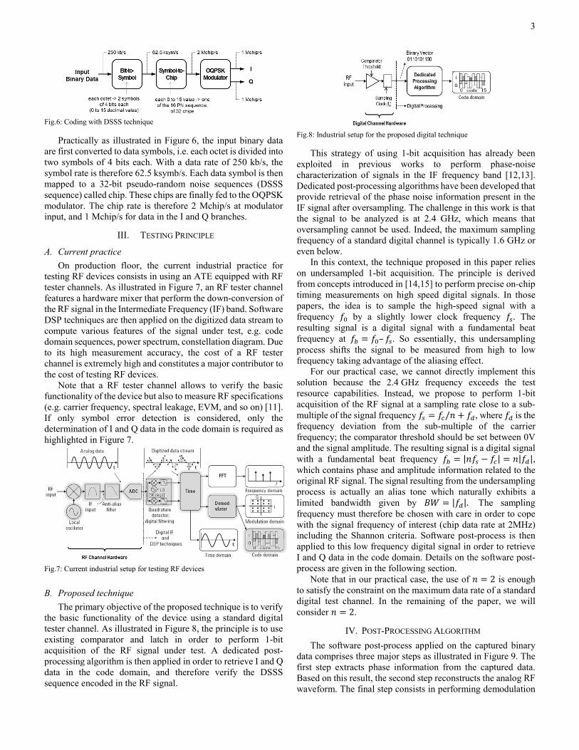
On production floor, the current industrial practice for testing RF devices consists in using an ATE equipped with RF tester channels. As illustrated in Figure 7, an RF tester channel features a hardware mixer that perform the down-conversion of the RF signal in the Intermediate Frequency (IF) band. Software DSP techniques are then applied on the digitized data stream to compute various features of the signal under test, e.g. code domain sequences, power spectrum, constellation diagram. Due to its high measurement accuracy, the cost of a RF tester channel is extremely high and constitutes a major contributor to the cost of testing RF devices.
Note that a RF tester channel allows to verify the basic functionality of the device but also to measure RF specifications (e.g. carrier frequency, spectral leakage, EVM, and so on) [11]. If only symbol error detection is considered, only the determination of I and Q data in the code domain is required as highlighted in Figure 7.
Fig.7: Current industrial setup for testing RF devices
B. Proposed technique
The primary objective of the proposed technique is to verify the basic functionality of the device using a standard digital tester channel. As illustrated in Figure 8, the principle is to use existing comparator and latch in order to perform 1-bit acquisition of the RF signal under test. A dedicated post-processing algorithm is then applied in order to retrieve I and Q data in the code domain, and therefore verify the DSSS sequence encoded in the RF signal.
Fig.8: Industrial setup for the proposed digital technique
This strategy of using 1-bit acquisition has already been exploited in previous works to perform phase-noise characterization of signals in the IF frequency band [12,13]. Dedicated post-processing algorithms have been developed that provide retrieval of the phase noise information present in the IF signal after oversampling. The challenge in this work is that the signal to be analyzed is at 2.4 GHz, which means that oversampling cannot be used. Indeed, the maximum sampling frequency of a standard digital channel is typically 1.6 GHz or even below.
In this context, the technique proposed in this paper relies on undersampled 1-bit acquisition. The principle is derived from concepts introduced in [14,15] to perform precise on-chip timing measurements on high speed digital signals. In those papers, the idea is to sample the high-speed signal with a frequency �� by a slightly lower clock frequency ��. The resulting signal is a digital signal with a fundamental beat frequency at �� = ��– ��. So essentially, this undersampling process shifts the signal to be measured from high to low frequency taking advantage of the aliasing effect.
For our practical case, we cannot directly implement this solution because the 2.4 GHz frequency exceeds the test resource capabilities. Instead, we propose to perform 1-bit acquisition of the RF signal at a sampling rate close to a sub-multiple of the signal frequency �� = ��/� + ��, where �� is the frequency deviation from the sub-multiple of the carrier frequency; the comparator threshold should be set between 0V and the signal amplitude. The resulting signal is a digital signal with a fundamental beat frequency �� = |��� − ��| = �|��|, which contains phase and amplitude information related to the original RF signal. The signal resulting from the undersampling process is actually an alias tone which naturally exhibits a limited bandwidth given by �� = |��|. The sampling frequency must therefore be chosen with care in order to cope with the signal frequency of interest (chip data rate at 2MHz) including the Shannon criteria. Software post-process is then applied to this low frequency digital signal in order to retrieve I and Q data in the code domain. Details on the software post-process are given in the following section.
Note that in our practical case, the use of � = 2 is enough to satisfy the constraint on the maximum data rate of a standard digital test channel. In the remaining of the paper, we will consider � = 2.
IV. POST-PROCESSING ALGORITHM
The software post-process applied on the captured binary data comprises three major steps as illustrated in Figure 9. The first step extracts phase information from the captured data. Based on this result, the second step reconstructs the analog RF waveform. The final step consists in performing demodulation

4
of the reconstructed waveform. Each one of these steps are detailed hereafter.
Fig.9: Processing steps for the determination of I and Q data from the binary vector captured by the ATE
A. Phase extraction
The goal of the first step is to retrieve the phase variation of the modulated signal from the binary vector captured by the ATE. This phase variation will then be used to build a reconstructed RF modulated signal.
Fig.10: Phase extraction from the binary vector captured by the ATE
Practically, the binary vector captured by the ATE is a sampled square wave �(���) (with �� = 1/�� the sampling period) with a fundamental beat frequency �� = |2�� − ��|. This signal is processed through several operations as illustrated in Figure 10.
First, the discrete-time signal �(���) is filtered by passing through a band pass filter centered on the square wave beat frequency in order to eliminate the harmonics introduced by 1-bit quantization. The resulting signal is a discrete-time sine wave �(���). Spline interpolation is applied to this signal in order to convert it into a continuous-time signal �(�). In the following step, the Hilbert Transform is computed in order to derive the analytic representation of the signal in the complex plane:
�(�) = �(�) + ���[�(�)] (1)
The instantaneous phase is then obtained with:
�(�) = atan ���[�(�)]
�(�)� (2)
Note that due to the ���� function, the computed instantaneous phase is a wrapped phase. By unwrapping �(�), we obtain a linear evolution of the instantaneous phase �(�), which can be expressed as:
�(�) = 2���� + �(�) (3)
where the first term corresponds to the linear phase of a signal with a fundamental beat frequency �� and the second term actually corresponds to the phase fluctuation �(�) of the modulated RF signal.
Finally, by using the theoretical value of the fundamental beat frequency and subtracting the first term, an estimation of the phase of the modulated RF signal is given by:
��(�) = Φ�(�) − 2�|2�� − ��|� (4)
An illustration of this phase estimation is given in Figure 11. Note that the under-sampling process introduces a quantization in the estimation of the phase fluctuation. The quantization step is directly related to the frequency deviation between sampling frequency �� and half the carrier frequency ��/2 with:
��� = 180° ∗����
���
�
��= 180° ∗
|��|
�� (5)
Fig.11: Estimated phase of the modulated RF signal ��(�)
B. Signal reconstruction
Once the phase fluctuation of the modulated signal is estimated, the emitted RF signal can be easily reconstructed by adding this fluctuation to the ideal instantaneous linear phase of the carrier:
�(�) = sin�2���� ± ��(�)� (6)
Note that depending whether the sampling frequency is chosen with a positive or negative deviation with respect to the carrier half-frequency, the estimated phase should be added or subtracted. In particular, ��(�) must be subtracted if �� > ��/2 and added otherwise.
So far, ideal conditions have been assumed for phase estimation of the modulated signal, i.e. the carrier frequency is known and there is a perfect synchronization between the digitizing channel and the circuit under test. Under such conditions, the estimated phase matches the actual phase of the modulated signal. However, such conditions are not easy to achieve in a practical environment. Most likely, the actual carrier frequency slightly differs from the ideal one, and capture clock is not synchronized. These imperfections introduce errors in the phase estimation, which can be expressed by:
��(�) = �(�) + 2������ + �� (7)
where �(�) is the actual phase fluctuation of the signal under test, ���� is the frequency difference between the assumed
carrier frequency and the actual one, and �� is an unknown phase offset related to absence of synchronization. Most likely, the reconstructed RF signal suffers from these imperfections and this is something we need to consider in the demodulation process.
C. Demodulation
The demodulation of the reconstructed RF signal involves several steps, as depicted in Figure 12. First, I and Q waveforms must be recovered from quadrature-modulated signal in the time-domain. The following step is then to extract I and Q binary data. Finally, parallel to serial conversion and ambiguity determination are applied to obtain the demodulated sequence.
Fig.12: Demodulation from the reconstructed RF signal
Ph
ase
(°)

5
1) Extraction of I and Q time-domain waveforms
To ensure right demodulation, frequency and phase offsets must be estimated first, so that carrier signal can be properly recovered. To illustrate this point, Figure 13 shows the constellation diagram of demodulated data in case of (i) an ideal signal, (ii) a signal with a phase offset of -30° and (iii) a signal with a frequency offset of 1kHz. It can be observed that the phase offset causes a rotation of the constellation while the frequency offset induces a spread of the data on the complete trigonometric circle. While phase offset can be easily identified and compensated, frequency error (even small) is more problematic and will definitely entail errors in the demodulated data. To cope with this issue, carrier recovery is usually employed, which permits to implement subsequent coherent demodulation.
(a) (b) (c) Figure 13 : Effect of phase and frequency offset on the constellation diagram of demodulated data: (a) ideal constellation, (b) phase offset, and (c) frequency offset of 1KHz
A classical technique to perform carrier recovery on QSPK/OQPSK modulated signals is the multiply-filter-divide technique, where the fourth power of the signal is computed to produce a signal with a harmonic component at 4�� and no phase modulation; this component is then filtered and divided by 4 to recover ��. Unfortunately, this technique does not apply in case of half sine pulse shaping, because of the continuous phase evolution instead of sharp transitions between the phase value.
Another possibility is the use of a Costas loop, which performs carrier frequency and phase recovery as well as demodulation. A Costas loop is a PLL-based circuit that uses coherent quadrature signals to measure phase error; this phase error is used to regulate the loop oscillator. When locked, quadrature signals correspond to the demodulated data.
In this work, we use a software model of the Costas loop based on the design proposed in [16] for QPSK modulation, adapted to deal with half sine pulse shaping. The modified architecture is given in Figure 14. The incoming RF signal is split in two I and Q branches. A delay of one-bit period (Tbit) is added on the I branch to compensate for the delay that has been added on the Q branch during the modulation process. Signals on the I and Q branches are then respectively multiplied by a VCO-generated tone and by a 90° shifted version of this tone. Low pass filtering removes the double frequency component to complete the demodulation. By calculating the difference between the absolute value of the demodulated I branch and Q branch, an error is obtained. This error passes through a loop filter and drives the VCO to achieve phase and frequency locking. In the locked state, ��(�) and ��(�) signals correspond
to the original (i.e. transmitted) I and Q waveforms.
Fig.14: Modified Costas loop for OQPSK with pulse shaping
Note that to improve the locking of the Costas loop, the VCO initial frequency should be close to the actual carrier frequency of the incoming signal. For this reason, we have implemented a first step which estimates this frequency. More precisely, we compute the spectrum of the squared RF signal, which exhibits two main components located at 2�� ± ����/2, where ���� is the 2MHz bit frequency. Taking the mean of these two components, we have an estimation of twice the actual carrier frequency. The accuracy of the estimation depends on FFT resolution but is typically in the range of few kHz. This estimation is not precise enough to perform correct demodulation but constitutes a useful starting point to set the VCO.
Technically, the Costas loop demodulation could be directly applied to the sine wave obtained by filtering the binary signal at ��. However, the beat frequency �� depends on the sampling frequency ��, resulting in a necessary adjustment of loop parameters accordingly. In addition, because the beat frequency can be relatively close to the chip rate, the correct operation of the loop is not ensured due to the filters limited order. Those are the main reasons for choosing a reconstruction at the RF carrier frequency ��. Another option could be to reconstruct the signal reconstruction at an arbitrary intermediate frequency �� suitable with the loop filters; this would reduce the number of points to process and save computation time.
2) Waveform-to-bit conversion
The following stage of the process consists in converting the reconstructed I and Q waveforms into a binary data and selecting one value each 2���� time interval. Practically, conversion to the binary format is done with a zero-crossing of ��(�) and ��(�) waveforms. The resulting binary signals are
then sampled with a 1/2����clock frequency. To ensure correct interpretation, the sampling should occur in the middle of the binary signals period. For this, a simple timing alignment process has been implemented, as illustrated in figure 15.
Fig.15: Waveform-to-bit conversion from reconstructed I and Q waveforms
To determine the proper timing alignment, we assume a sampling clock with an initial delay ������ = 0. Then for each

6
binary signal, we compute the time difference �� between every signal transition and the following edge of the sampling clock. The mean of these differences over the complete sequence (��� ) corresponds to the initial delay that must be applied on the sampling clock to align the sampling clock with corresponding binary signal. Then, an additional delay of ���� is simply added (������ = ��� + ����) to sample the data in the middle of the
binary signal period. The different steps of the waveform-to-bit conversion procedure are illustrated in Figure 16 for an example of reconstructed ��(�) waveform.
Fig.16 : Illustration of waveform-to-bit conversion for an example of reconstructed ��(�) waveform
3) Ambiguity determination and parallel-to-serial conversion
The final stage simply consists in translating the binary I and Q data into chips with parallel-to-serial conversion. The DSSS sequences can then be identified within the demodulated chips. Unfortunately, the Costas loop locks with a � ∗ �/2 phase ambiguity. Therefore, the determined values for I and Q data might be complemented (or not). This produces four possible combinations for the demodulated data, i.e. ��, ��̅, ��� and ��̅�. To remove this phase ambiguity, we search for existing DSSS sequences in the demodulated data assuming the four combinations. When a match is found, the corresponding combination is retained all along.
V. SIMULATION RESULTS
A. Simulation setup
To validate the technique, a simulation bench has been developed in Matlab®, which involves the Circuit Under Test (CUT), the digital ATE channel and the post-processing algorithm. Chief interests of evaluating the technique in simulation is that, (i) we can perfectly control the characteristics of the signal generated by the CUT, (ii) we have access to internal information, e.g. the time-domain �(�) and �(�) signals, which are not available when dealing with physical RF signals, and (iii) we can introduce known imperfections both in the signal under test and in the test equipment.
The complete simulation setup is summarized in Figure 17. Basically, the Circuit Under Test is modelled as an OQPSK modulator with half sine pulse shaping and the digital ATE channel is modelled with a level-crossing operation followed
by a sampling operation. Three different types of imperfections that may affect the quality of the signal delivered by the Circuit Under Test have been considered: IQ imbalance, phase noise and amplitude noise. We have also considered two different types of imperfections on the test equipment: jitter in the sampling clock and offset on the comparator threshold.
Fig.17: Simulation setup
This simulation setup has been used to analyze a modulated signal with a carrier frequency �� = 2.405 ���. Undersampled 1-bit acquisition is performed with a sampling frequency �� =1.21212 ���, which corresponds to a frequency deviation �� = 9.62 ���. The spectrum of the signal is therefore transposed around 2�� = 19.2 ���. Note that according to Eq.(5), the smaller the frequency deviation ��, the smaller the quantization step ��� in the phase estimation and the more
precise the signal reconstruction. On the other hand, the frequency deviation should not be too small in order to preserve the measurement bandwidth, i.e. the fundamental frequency of the transposed spectrum must be higher than twice the chip rate of 2 MHz. Here choosing �� = 9.62 ��� provides enough margin with respect to the chip rate and a satisfactorily small quantization step ��� = 1.4°.
B. Validation under ideal conditions
First validation has been realized under ideal conditions, i.e. without any imperfections introduced in the CUT nor the test equipment. The result of the phase extraction process is shown in Figure 18, which compares the phase of the RF signal generated by the OQPSK modulator to the phase estimated from the undersampled digital capture. A very good agreement can be observed with a difference that remains below the theoretical quantification error ��� of 1.4°, demonstrating the
ability of the technique to perform accurate phase estimation.
Fig.18: Comparison between original and extracted phases
Ph
ase
(°)
Err
or
(°)

7
The result of the demodulation process is illustrated in Figure 19, which compares the waveform �(�) present in the modulator to the waveform ��(�) reconstructed from the analysis of the undersampled digital capture. Here again a very good agreement is observed with an rms error of 1.66% and a maximum error that does not exceed 5%, which validates the ability of the proposed technique to properly demodulate the signal.
Fig.19: Comparison between original and reconstructed I-waveforms
C. Study of robustness
To further validate the method, we have investigated its robustness to different imperfections that may affect either the signal delivered by the circuit under test or the signal captured by the test equipment.
1) IQ balance
First, IQ imbalance introduces fluctuations in the envelope of the modulated RF signal. Various simulations have been realized varying the level of IQ imbalance from 0% (ideal case) to 50% (exaggerated case). Results show that the processing algorithm is very robust to the presence of IQ imbalance since it properly works for a large range up to 40%; beyond 40%, some errors appear in the demodulated data.
The impact of IQ imbalance can be observed on the response of the Costas loop. As illustrated in Figure 20 (exaggerated case of 40% IQ imbalance), oscillations appear in the phase correction operated by the loop, but the general trend is preserved, and the loop remains locked in the same state. Errors observed in case of imbalance superior to 40% actually come from instability of the Costas loop which does not remain locked in the same quadrant during the demodulation.
Fig.20: Costas loop phase correction without and with 40% IQ imbalance
2) Carrier phase noise
The presence of phase noise in the carrier has been investigated. For this, we have used the model described in [12] to introduce 1/f2 phase noise with a level of about -80dBc/Hz at a frequency offset of 100kHz. The impact of phase noise is not directly visible in the modulated RF signal, but can be observed on the Costas loop response, as shown in Figure 21. Phase noise
present in the carrier is tracked and compensated by the Costas loop. The processing algorithm is not affected.
Fig.21: Costas loop phase correction without and with phase noise
3) Noisy RF signal
In order to study the effects of a noisy RF signal, we have performed a number of simulations varying the level of the Gaussian noise added at the modulator output. Results show that the demodulation process is not sensitive to the presence of noise up to extremely high noise level. Indeed because of the limited bandwidth of the undersampled signal the binary waveform resulting from the digital capture exhibit clean transitions in presence of moderate noise, as depicted in Figure 22.a with SNR of 60dB. Multiple transitions appear in the binary signal when the noise level increases, as illustrated in Figure 22.b with SNR of 35dB. Note that these multiple transitions do not necessarily entail errors in the demodulated data, because of the use of a bandpass filter in the phase extraction procedure.
(a) SNR=60dB (b) SNR=35dB
Fig.22 : Result of the digital capture with a noisy RF signal
To further illustrate this point, we have recorded the number of errors observed on a sequence of 2,048 bits for different levels of injected noise. Results are summarized in Figure 23, which reports the percentage of errors with respect to the signal SNR. Errors occur only when SNR degrades below 27dB. Obviously, such a high level of noise is unrealistic in the test production environment, validating the robustness of the technique to the presence of noise.
Fig.23 : Percentage of errors as function of the RF signal SNR
4) ATE jitter
Typically, standard digital ATE channels are specified with a jitter of few ps. To verify the robustness of the technique to the presence of such jitter, simulations have been performed by
t(s) 10-4
0 0.5 1 1.5 2 2.5-0.5
0
0.5
1 Without IQ imbalance
With IQ imbalance
t(s) 10-4
0.5 1 1.5 2 2.5
0
0.2
0.4
0.6
Without phase noise
With phase noise

8
injecting a random jitter on the ATE sampling clock with standard deviation ranging from 1ps up to 70ps. The correct operation of the processing algorithm has been observed in all cases. As illustrated in Figure 24, the presence of jitter increases the phase measurement error, but is small enough to permit correct demodulation.
Fig.24: Difference between original phase and extracted phase without and with ATE jitter
5) ATE comparator offset
Finally, the last imperfection we have considered is an offset on the comparator threshold in the ATE. Theoretically, the process is independent of the voltage level, provided that this voltage remains inferior to the signal amplitude.
To check this point, simulations have been performed for different values of the comparator threshold. Figure 25 reports the difference between the original and the reconstructed waveforms for the two different thresholds (0V and 50%); in both cases, the difference is very small with a maximum error that does not exceed 5%.
Fig.25: Influence of the ATE comparator threshold
Practically, we recommend setting the comparator threshold between 0 and 80% of the signal amplitude. Indeed, a too high comparator threshold may lead to multiple transitions in the binary signal in case of a noisy modulated RF signal.
VI. EXPERIMENTAL RESULTS
The proposed method has been tested using a real ZigBee transceiver from NXP semiconductors. Practically, a test pattern composed of the 16 DSSS sequences is transmitted and the TX RF port is captured with a standard digital channel of V93000 ATE (PS1600 Pinscale® channel board), with a sampling frequency �� = 1.21212GHz; the comparator threshold was set to 50% of the amplitude of the RF signal. Data are then transferred from the ATE to a computer to perform the software post-process. This experimental setup is illustrated in Figure 26.
Fig.26 : Experimental setup
Figure 27 shows the result of the digital acquisition of the RF signal delivered by the circuit when using the tester hardware. It can be observed that the captured binary signal exhibits relatively clean transitions, corresponding to the case of an RF signal with moderate noise as studied in simulation.
Fig.27 : Result of a digital acquisition with a PS1600 Pin Scale channel of V93000 ATE
Figure 28 shows the response of the Costas loop to the reconstructed RF signal. It can be observed that the loop locks and performs phase and frequency offset correction as expected.
Figure 28: Costas loop phase correction
Finally, results of the post-processing algorithm are
summarized in Figure 29. The first graph shows reconstructed waveforms ��(�) and ��(�); these waveforms exhibit the
expected behavior of I and Q signals generated with half sine pulse shaping. The second and third graphs correspond to the binary interpretation of these signals, for I and Q data respectively. After parallel-to-serial conversion and ambiguity determination, we have been able to recover the test pattern composed of the 16 DSSS sequences. This experiment demonstrates the validity of the proposed technique to implement low-cost symbol error detection for RF ZigBee transmitters using only a standard digital tester channel.
t(s) 10-4
1.07 1.08 1.09 1.1 1.11 1.12 1.13 1.14
-10
-5
0
5
10
15
Without jitter
With 5 ps jitter
With 30 ps jitter

9
Fig.29: Demodulated chips from capture on standard digital channel
VII. CONCLUSION
In this paper, we have developed an original technique that permits to analyze 2.4 GHz signals modulated with OQPSK and half-sine pulse shaping using only standard digital test resources. It relies on undersampled 1-bit acquisition of the RF signal. A dedicated post-process algorithm is then applied on captured binary data which permits to retrieve the transmitted symbol sequence.
The method has been first validated through Matlab® simulations under both ideal and non-ideal conditions. Results have shown proper operation and high level of robustness. The method has also been proven through hardware measurements involving both a standard digital tester channel and a ZigBee transceiver from NXP. Obtained results fully validate its ability to retrieve the symbol sequence generated by the transceiver.
Regarding the capture and processing time, which is an important contributor to the total cost of the test, our technique only introduces an overhead consisting in reconstructing the RF signal from the 1-bit acquisition. All subsequent processing is the same as for a standard test. This overhead increases the test time by about 14% but can be balanced by a multisite approach since a large number of digital channels are usually available on ATEs.
At this point, one must point out that symbol error detection is obviously not enough to address a complete RF transmitter test as specified in the 802.15 standard. Still, a practical application of this work can be to perform a preliminary screening test at wafer level using standard digital tester resources, and then perform performance measurements using RF tester resources only during the final test. More generally, the building blocks introduced and validated in this study constitute a foundation for further developments dedicated to phase and amplitude measurements, providing keys towards the implementation of spectral leakage and EVM tests.
To summarize, this initial study opens a new way towards low-cost functional testing of RF ZigBee transmitters by lowering the requirement on high-end and expansive RF hardware resources and offering the possibility to implement multi-site testing. It is still an ongoing work; future developments will concentrate on the evolution of the post-processing algorithm to include performance measurements and optimization for practical integration in the production test flow.
REFERENCES
[1] Test and Test Equipment, International Technology Roadmap for Semiconductors 2011 Edition, 2011.
[2] F. Demmerle, "Integrated RF-CMOS Transceivers challenge RF Test," Proc. IEEE International Test Conference, pp. 1-8, 2006.
[3] C.C. Su et al., “Dynamic analog testing via ATE digital test channels”, Proc. IEEE Asian Test Symp., pp. 308-312, 2004.
[4] N. Pous et al., “ Exploiting zero-crossing for the analysis of FM modulated analog/RF signals using digital ATE”, Proc. IEEE Asian Test Symp., pp. 261-266, 2009.
[5] N. Pous et al., J.,"A Level-Crossing Approach for the Analysis of RF Modulated Signals using only Digital Test Resources", J. of Electronic Testing: Theory and App. (JETTA), vol. 27, no. 3, pp 289-303, 2011
[6] F. Azais, L. Latorre, "Low-cost SNR estimation of analog signals using standard digital automated test equipment (ATE)," Proc. IEEE Int. New Circuits and Systems Conf (NEWCAS), pp. 197-200, 2012
[7] I. Kore et al., "Multi-site test of RF transceivers on low-cost digital ATE," Proc. IEEE International Test Conference (ITC), pp. 1-10, 2011.
[8] C. H. Peng et al., "A novel RF self test for a combo SoC on digital ATE with multi-site applications," Proc. IEEE International Test Conference (ITC), pp. 1-8, 2014.
[9] M. Ishida K. Ichiyama, "An ATE System for Testing RF Digital Communication Devices With QAM Signal Interfaces," IEEE Design & Test, vol. 33, no. 6, pp. 15-22, 2016.
[10] T. Vayssade et al., “Low-cost functional test of a 2.4 GHz OQPSK transmitter using standard digital ATE”, Proc. IEEE Int’l On-Line Test Conferance (IOLTS), pp.1-6, 2018.
[11] K. Ichiyama et al., "A functional test of 2-GHz/4-GHz RF digital communication device using digital tester," Proc. IEEE International Test Conference (ITC), pp. 1-10, 2013.
[12] S. David-Grignot, F. Azais, L. Latorre, F. Lefevre, "Low-cost phase noise testing of complex RF ICs using standard digital ATE," Proc. IEEE International Test Conference (ITC), pp. 1-9, 2014.
[13] S. David-Grignot, F. Azaïs, L. Latorre, F. Lefevre, "A new technique for low-cost phase noise production testing from 1-bit signal acquisition," Proc.IEEE European Test Symposium (ETS), pp. 1-6, 2015.
[14] J-L Huang, K-T Cheng, "An on-chip short-time interval measurement technique for testing high-speed communication links," Proc. IEEE VLSI Test Symposium (VTS), pp. 380-385, 2001.
[15] S. Sunter, A. Roy, "On-chip digital jitter measurement, from megahertz to gigahertz," IEEE Design & Test of Computers, vol. 21, no. 4, pp. 314-321, 2004.
[16] M. Tytgat, M. Steyaert, P. Reynaert, "Time Domain Model for Costas Loop Based QPSK Receiver," PRIME; Conference on Ph.D. Research in Microelectronics & Electronics, pp. 1-4, 2012.