LogiCORE IP Video On-Screen Display v1 · PDF fileLogiCORE IP Video On-Screen Display v1.0 ......
40
DS728 September 16, 2009 www.xilinx.com 1 Product Specification © 2009 Xilinx, Inc. XILINX, the Xilinx logo, Virtex, Spartan, ISE and other designated brands included herein are trademarks of Xilinx in the United States and other countries. All other trademarks are the property of their respective owners. Introduction The Xilinx Video On-Screen Display LogiCORE™ IP provides a flexible video processing block for alpha blending and compositing as well as simple text and graphics generation. Support for up to eight layers using a combination of external video inputs (from frame buffer) and internal graphics controllers (includ- ing text generators) is provided. Supports image sizes up to 4kx4k with YUVA 4:4:4 or 4:2:2 and RGBA image formats up to 60fps. The core is programmable through a comprehensive register interface for setting and con- trolling screen size, background color, layer position, and more using logic or a microprocessor. A compre- hensive set of interrupt status bits is provided for pro- cessor monitoring. The LogiCORE IP is provided with two different interfaces: General Purpose Processor and EDK pCore (including device driver). Features • Supports video frame sizes up to 4096x4096 pixels • Supports video frame rates up to 60fps. • Supports the YUVA-4:4:4, YUVA-4:2:2 and the RGBA color-spaces (with alpha) at 8bits per pixel (color-spaces can be mixed with addition of chroma-resampler and color-space converter) • Supports alpha-blending 8 video/graphics layers. • Provides programmable background color • Provides programmable layer position, size and z-plane order • Generates filled and outlined transparent boxes • Generates text with 1-bit or 2-bit per pixel color depth • Provides configurable internal text string memory • Provides configurable internal font memory for 8x8 or 16x16 pixel fixed distance fonts • Provides scaling text by 1x, 2x, 4x or 8x • Supports graphics color palette of 16 or 256 colors • Provides processor interfaces for EDK pCore and General Purpose Processor. • Supports easy integration with other Xilinx Video IP Cores including the VFBC, VDMA and Video Timing Controller Applications Applications range from broadcast and consumer to automotive, medical and industrial imaging and can include: • Video Surveillance • Machine Vision • Video Conferencing • Set-top box displays Overview The Xilinx Video On-Screen Display LogiCORE IP pro- duces output video from multiple external video sources as well as from multiple internal graphics con- trollers. Each graphics controller generates simple text and graphics overlays. Each video and graphics source is assigned an image layer. Up to eight image layers can be dynamically positioned, resized, brought forward or backward and combined using alpha-blending. Alpha-blending is the convex combination of two image layers allowing for transparency. Each layer in the OSD has a definite Z-plane order, or conceptually, each layer resides closer or farther from the observer having a different depth. Thus, the image and the image directly “over” it are blended. The order and amount of blending is programmable in real-time. An example Xilinx Video On-Screen Display Output is shown in Figure 1. LogiCORE IP Video On-Screen Display v1.0 DS728 September 16, 2009 Product Specification
Transcript of LogiCORE IP Video On-Screen Display v1 · PDF fileLogiCORE IP Video On-Screen Display v1.0 ......

DS728 September 16, 2009 www.xilinx.com 1Product Specification
© 2009 Xilinx, Inc. XILINX, the Xilinx logo, Virtex, Spartan, ISE and other designated brands included herein are trademarks of Xilinx in the United States and other countries. All other trademarks are the property of their respective owners.
Introduction The Xilinx Video On-Screen Display LogiCORE™ IPprovides a flexible video processing block for alphablending and compositing as well as simple text andgraphics generation. Support for up to eight layersusing a combination of external video inputs (fromframe buffer) and internal graphics controllers (includ-ing text generators) is provided. Supports image sizesup to 4kx4k with YUVA 4:4:4 or 4:2:2 and RGBA imageformats up to 60fps. The core is programmable througha comprehensive register interface for setting and con-trolling screen size, background color, layer position,and more using logic or a microprocessor. A compre-hensive set of interrupt status bits is provided for pro-cessor monitoring. The LogiCORE IP is provided withtwo different interfaces: General Purpose Processor andEDK pCore (including device driver).
Features• Supports video frame sizes up to 4096x4096 pixels
• Supports video frame rates up to 60fps.
• Supports the YUVA-4:4:4, YUVA-4:2:2 and the RGBA color-spaces (with alpha) at 8bits per pixel (color-spaces can be mixed with addition of chroma-resampler and color-space converter)
• Supports alpha-blending 8 video/graphics layers.
• Provides programmable background color
• Provides programmable layer position, size and z-plane order
• Generates filled and outlined transparent boxes
• Generates text with 1-bit or 2-bit per pixel color depth
• Provides configurable internal text string memory
• Provides configurable internal font memory for 8x8 or 16x16 pixel fixed distance fonts
• Provides scaling text by 1x, 2x, 4x or 8x
• Supports graphics color palette of 16 or 256 colors
• Provides processor interfaces for EDK pCore and General Purpose Processor.
• Supports easy integration with other Xilinx Video IP Cores including the VFBC, VDMA and Video Timing Controller
ApplicationsApplications range from broadcast and consumer toautomotive, medical and industrial imaging and caninclude:
• Video Surveillance
• Machine Vision
• Video Conferencing
• Set-top box displays
OverviewThe Xilinx Video On-Screen Display LogiCORE IP pro-duces output video from multiple external videosources as well as from multiple internal graphics con-trollers. Each graphics controller generates simple textand graphics overlays. Each video and graphics sourceis assigned an image layer. Up to eight image layers canbe dynamically positioned, resized, brought forward orbackward and combined using alpha-blending.
Alpha-blending is the convex combination of twoimage layers allowing for transparency. Each layer inthe OSD has a definite Z-plane order, or conceptually,each layer resides closer or farther from the observerhaving a different depth. Thus, the image and theimage directly “over” it are blended. The order andamount of blending is programmable in real-time.
An example Xilinx Video On-Screen Display Output isshown in Figure 1.
LogiCORE IP Video On-ScreenDisplay v1.0
DS728 September 16, 2009 Product Specification

LogiCORE IP Video On-Screen Display v1.0
2 www.xilinx.com DS728 September 16, 2009Product Specification
Here we show an example OSD output with multiple video and graphics layers. The three video layers(Video 1, 2 and 3) can be still images or live video and are combined with transparency to the program-mable background color. Simple boxes and text are generated with one or multiple internal graphicscontrollers (as shown with the yellow text and menu buttons) and also blended with the other layers.One other video layer (the Xilinx Logo), can be generated from on-chip or external memory, showingthat the OSD output can be easily extended with external logic, a microprocessor or memory storage.
Basic ArchitectureThe Xilinx On-Screen Display LogiCORE IP reads 2D video image data in raster order from up to eightsources. Each data source can be configured to be a FIFO interface or an internal graphics controller. Ifa FIFO interface is selected, ports on the OSD are available for connecting to and reading data from theXilinx Video Frame Buffer Controller or from the Video Direct Memory Access Controller. These portsare also generic enough for easy integration with any FIFO. If an internal graphics controller is selectedto be a source, then the OSD automatically handles interfacing to each graphics controller.
Pixel data from each source is combined using alpha-blending. The resultant output is a 2D videoimage stream that can be presented to one of two output interfaces – to a FIFO interface or to a XilinxStreaming Video Interface (XSVI). If a FIFO interface is used, the output FIFO almost full flag and theinput FIFO empty flags (from each FIFO input source) will halt operation of the OSD until cleared. If anXSVI interface is used, the data is presented on the output along with video synchronization signals(Vertical Blank, Horizontal Blank, etc.). The data is presented at the time required by the synchroniza-tion signals, and thus, the input FIFO empty flags are ignored. Care must be taken to make sure eachinput FIFO does not underflow.
X-Ref Target - Figure 1
Figure 1: Example of OSD Output
DS728 September 16, 2009 www.xilinx.com 3Product Specification
LogiCORE IP Video On-Screen Display v1.0
Only one output interface can be selected. The OSD cannot drive both interfaces at the same time.Please see the "Port Descriptions" section for more information on both the output FIFO (VFBC WriteData Interface) and the output XSVI interfaces.
The Xilinx On-Screen Display also requires an input Xilinx Streaming Video Interface. The OSD doesnot receive video data from this interface. This interface is only used to receive the horizontal/verticalblank and sync signals as well as an active video signal. The horizontal and vertical sync signals are notused internally to the OSD and are only delayed and presented on the output XSVI interface for usewith driving external display hardware. The same is true for the active video signal and is used only todelineate the presence of valid output. Only the horizontal and vertical blank signals are used inter-nally to the OSD for control and synchronization of frame data.
Please see the Xilinx Video Timing Controller data sheet for more information on video timing signals.
The use of specific video timing signals requires that the input data is always present when requested(the OSD will not look at the input FIFO empty flags) if an XSVI interface is used. If an output FIFOinterface is used, it is required that the input and output FIFO flags do not delay the operation of OSDtoo often, as this may cause frames to not be completely processed. Specific interrupt status bits willalert such errors.
An example OSD configuration with three data sources (layers) is shown in Figure 2. Data for layer 0and layer 1 are read from input FIFOs. Data for layer 2 are read from a graphics controller instance. X-Ref Target - Figure 2
Figure 2: Example OSD Block Diagram
LogiCORE IP Video On-Screen Display v1.0
4 www.xilinx.com DS728 September 16, 2009Product Specification
In addition to the video data interfaces, the Xilinx On-Screen Display has a control interface for settingregisters that control the background color and screen size. The size, (x,y) position and priority(Z-plane order) of each layer can also be configured. Registers for overriding pixel based alpha valueswith a global alpha and for enabling/disabling layers are also provided.
All control registers can be set dynamically in real time. The OSD internally double-buffers all controlregisters every frame. Thus, control registers can be updated without introducing artifacts on screen. Inaddition, the OSD provides a “Register Update Enable” bit in the control register that allows control-ling the timing of the double-buffered register updates for further flexibility.
A 32-bit interrupt status register output is also provided that flags internal errors or general events thatmay require host processor intervention. Interrupt status bits flag events for vertical blanking start andend, frame error, frame complete, input FIFO underflow, output FIFO overflow and graphics controllererrors (discussed later).
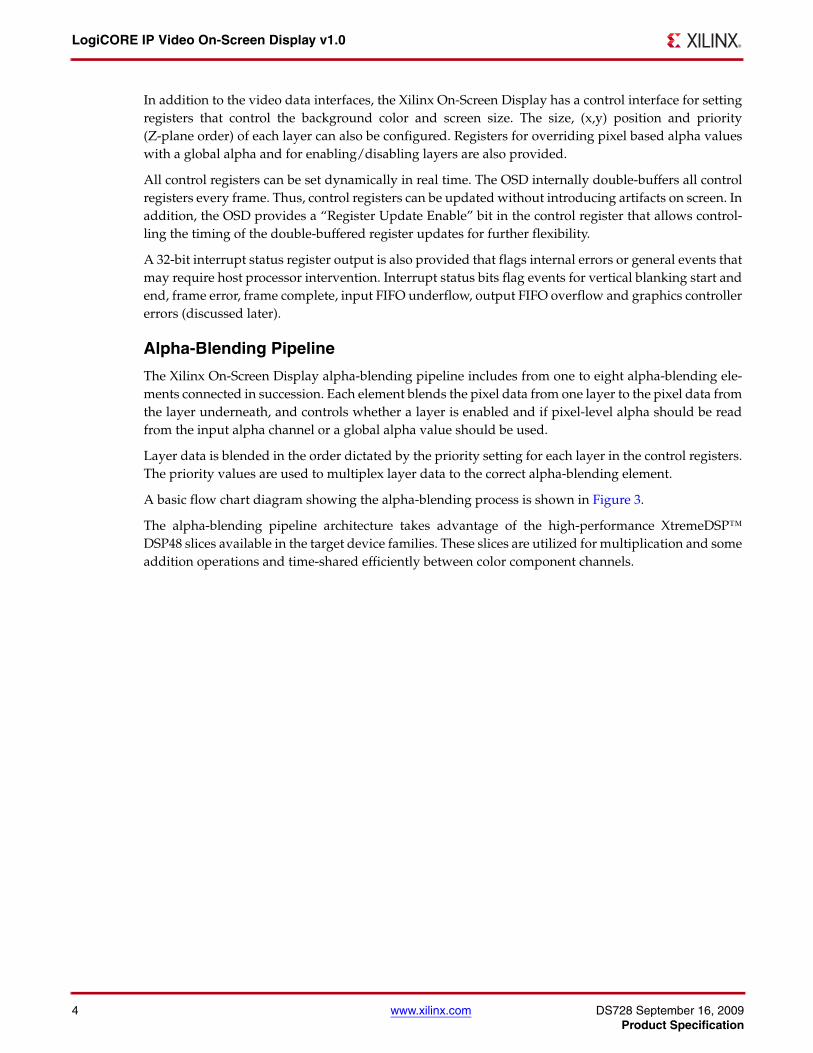
Alpha-Blending Pipeline
The Xilinx On-Screen Display alpha-blending pipeline includes from one to eight alpha-blending ele-ments connected in succession. Each element blends the pixel data from one layer to the pixel data fromthe layer underneath, and controls whether a layer is enabled and if pixel-level alpha should be readfrom the input alpha channel or a global alpha value should be used.
Layer data is blended in the order dictated by the priority setting for each layer in the control registers.The priority values are used to multiplex layer data to the correct alpha-blending element.
A basic flow chart diagram showing the alpha-blending process is shown in Figure 3.
The alpha-blending pipeline architecture takes advantage of the high-performance XtremeDSP™DSP48 slices available in the target device families. These slices are utilized for multiplication and someaddition operations and time-shared efficiently between color component channels.
DS728 September 16, 2009 www.xilinx.com 5Product Specification
LogiCORE IP Video On-Screen Display v1.0
X-Ref Target - Figure 3
Figure 3: Alpha-Blending Pipeline Flow Chart
LogiCORE IP Video On-Screen Display v1.0
6 www.xilinx.com DS728 September 16, 2009Product Specification
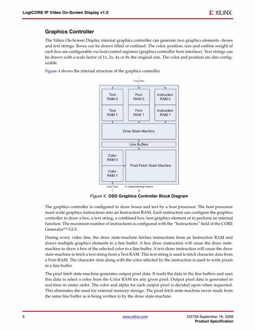
Graphics Controller
The Xilinx On-Screen Display internal graphics controller can generate two graphics elements –boxesand text strings. Boxes can be drawn filled or outlined. The color, position, size and outline weight ofeach box are configurable via host control registers (graphics controller host interface). Text strings canbe drawn with a scale factor of 1x, 2x, 4x or 8x the original size. The color and position are also config-urable.
Figure 4 shows the internal structure of the graphics controller.
The graphics controller is configured to draw boxes and text by a host processor. The host processormust write graphics instructions into an Instruction RAM. Each instruction can configure the graphicscontroller to draw a box, a text string, a combined box/text graphics element or to perform an internalfunction. The maximum number of instructions is configured with the “Instructions” field of the COREGenerator™ GUI.
During every video line, the draw state-machine fetches instructions from an Instruction RAM anddraws multiple graphics elements to a line buffer. A box draw instruction will cause the draw state-machine to draw a box of the selected color to a line buffer. A text draw instruction will cause the drawstate-machine to fetch a text string from a Text RAM. This text string is used to fetch character data froma Font RAM. The character data along with the color selected by the instruction is used to write pixelsin a line buffer.
The pixel fetch state-machine generates output pixel data. It reads the data in the line buffers and usesthis data to select a color from the Color RAM for any given pixel. Output pixel data is generated inreal-time in raster order. The color and alpha for each output pixel is decided upon when requested.This eliminates the need for external memory storage. The pixel fetch state-machine never reads fromthe same line buffer as is being written to by the draw state-machine.
X-Ref Target - Figure 4
Figure 4: OSD Graphics Controller Block Diagram
DS728 September 16, 2009 www.xilinx.com 7Product Specification
LogiCORE IP Video On-Screen Display v1.0
Notice that for each memory type (Instruction, Color, Text and Font), there are two memories – RAM 0and RAM 1. This duplication allows the host processor to write to one memory while the graphics con-troller is reading from another. This eliminates screen artifacts while the processor is configuring thegraphics controller.
Memory boundaries are conceptual only. Some graphics controller memories may be efficiently com-bined in order to save Block RAM or Distributed RAM storage.
Each graphics controller has a set of parameters that controls its configuration. These parameters affectthe size of each memory and the resources used by the Xilinx On-Screen Display. See Table 1, "COREGenerator GUI Field Descriptions" for more information on the graphics controller parameters.
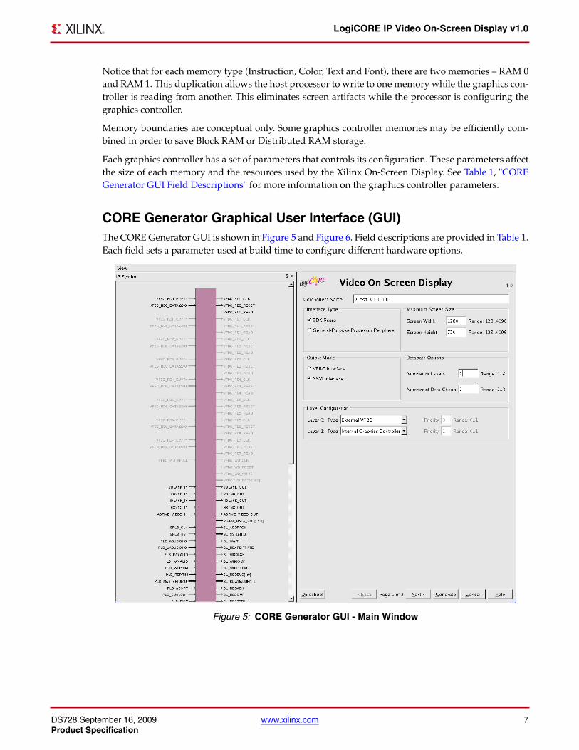
CORE Generator Graphical User Interface (GUI)The CORE Generator GUI is shown in Figure 5 and Figure 6. Field descriptions are provided in Table 1.Each field sets a parameter used at build time to configure different hardware options. X-Ref Target - Figure 5
Figure 5: CORE Generator GUI - Main Window

LogiCORE IP Video On-Screen Display v1.0
8 www.xilinx.com DS728 September 16, 2009Product Specification
Note: The Graphics Controller Options Window is available only if the Layer Type is set to “Internal Graphics Controller.”
X-Ref Target - Figure 6
Figure 6: Core Generator GUI - Graphics Controller Options Window
Table 1: CORE Generator GUI Field Descriptions
Field Description
Global Parameters
Component Name The component name is used as the base name of output files generated for the module. Names must begin with a letter and must be composed from characters: a to z, 0 to 9and “_”.
Interface Type The On-Screen Display is generated with one of two control interfaces.• EDK pCore Interface: CORE Generator generates the core as a
pCore which can be easily imported into an EDK project as a hardware peripheral. The core registers can be programmed in real-time via MicroBlaze™ and the Processor Local Bus (PLB). See the "EDK pCore (PLB) Interface" section.
• General Purpose Processor Interface: CORE Generator generates a set of ports that can be used to program the core. See the "General Purpose Processor Interface" section.
DS728 September 16, 2009 www.xilinx.com 9Product Specification
LogiCORE IP Video On-Screen Display v1.0
Maximum Screen Size This field configures the maximum allowed screen size. The Maximum screen width and maximum screen height are configurable. Changing this field affects several counters, comparators and memory (Block RAM) usage. Increased screen size increases resource usage. Valid range for both Screen Width and Screen Height is {128 .. 4096}.
Output Mode This field configures the On-Screen Display for one of two output interfaces.• VFBC Interface: The core is generated with the Video Frame Buffer
Controller ports enabled. These ports are a generic read FIFO with empty flag. See the "Write FIFO Interface" section.
• XSVI Interface: The core is generated with the Xilinx Streaming Video Interface port enabled. See the "Xilinx Streaming Video Interface (XSVI)" section.
• Corresponds to the C_OUTPUT_MODE Parameter of the EDK pCore.
Number of Layers This field configures the number of layers to alpha blend together. Each layer can be configured to read data from the FIFO inputs or from one of the internal Graphics Controllers. Valid range is (1 .. 8).
Corresponds to the C_NUM_LAYERS Parameter of the EDK pCore.
Number of Data Channels This field configures the number of data channels. Valid values are 2 and 3.2 = Two 8bit data channels. Typically used for YUV 4:2:2 data. Either channel can be luminance (Y) or chrominance (Cb,Cr) channels if no internal Graphics Controller is used. If using a Graphics Controller layer, the Graphics Controller outputs luminance (Y) on channel 0 and chrominance (Cb,Cr) on channel 1.3 = Three 8-bit data channels. Used for RGB and YUV 4:4:4 data. This mode is color component agnostic. Each channel can be configured for any color component. Corresponds to the C_NUM_DATA_CHANNELS Parameter of the EDK pCore.
Layer Configuration – Layer # Type These fields configure the type, or data source, of each layer, one field for each layer. Each layer is numbered from 0 to 7. The maximum number of layers is set by the Number of Layers field. Two data sources are valid:• External VFBC: This is a Read FIFO interface with data, read enable
and empty ports. Typically connected to the Video Frame Buffer Controller or the Video DMA read FIFO interfaces. See the "Read FIFO Interface" section.
• Internal Graphics Controller: If the layer is configured for this type, then the Read FIFO interface inputs are ignored and all data is generated and read from an internal Graphics Controller.
Graphics Controller Parameters
Instructions This field configures the maximum number of Graphics Controller instructions that can be executed per frame. Increasing this number increases the number of Block RAMs utilized.
Instruction Set This field configures which instructions are valid for the Graphics Controller implementation. Two instructions are currently configurable: box and text. Other instructions, including NoOp, are always available.
Number of Colors This field configures the size of the color palette used by the Graphics Controller. Valid values are 16 and 256.
Table 1: CORE Generator GUI Field Descriptions (Cont’d)
Field Description

LogiCORE IP Video On-Screen Display v1.0
10 www.xilinx.com DS728 September 16, 2009Product Specification
Port DescriptionsTable 2 shows the IO signals on the Xilinx Video On-Screen Display.
Color Memory Type This field configures how the color palette is implemented in hardware, as Distributed RAM, as Block RAM or Auto-Configured. In auto-configuration mode, distributed RAM will be used if the color palette is small enough. The RAM type can be overridden if it is known which type is preferred for the application.
Number of Characters This field configures the number of characters to be stored within the internal Font RAM. This field, along with the Character Width, Character Height, ASCII Offset and Bit per Pixel fields, affects the overall size of the Font RAM.
Character Width This field configures the width of each character. The width is in pixels. Valid values are 8 and 16.
Character Height This field configures the height of each character. The height is in video lines. Valid values are 8 and 16.
ASCII Offset This field configures the ASCII value of the first location in the Font RAM. This is useful if it is known that certain ASCII values will not be used.
Bits per Pixel This field configures the bits per pixel of each character. Valid values are 1 and 2.1 = One bit per pixel. This yields a foreground and a background color for each character.2 = Two bits per pixel. This allows each character pixel to be programmed to one of four different colors.
Number of Strings This field configures the maximum number of strings to be stored within the Text RAM. This field, along with the Maximum String Length field, affects the overall size of the Text RAM. The maximum number of strings cannot exceed 255.
Maximum String Length This field configures the maximum string length allowed for each string within the Text RAM. The maximum string length cannot exceed 255.
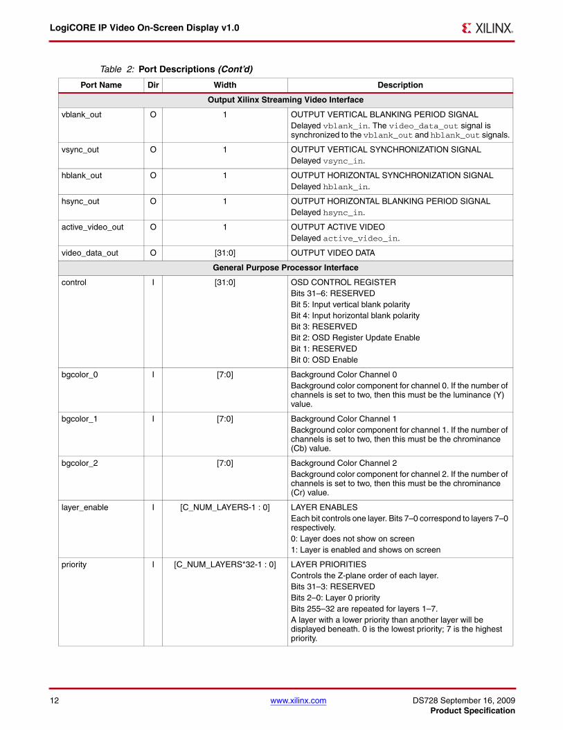
Table 2: Port Descriptions
Port Name Dir Width Description
clk I 1 CORE CLOCKCore clock (active high edge).
sclr I 1 SYNCHRONOUS CLEAR/RESETSystem synchronous reset (active high). Asserting sclr synchronously with clk resets the Xilinx On- Screen Display internal state machines. sclr has priority over ce.
ce I 1 CLOCK ENABLEUsed to halt processing and hold current values.
Input Xilinx Streaming Video Interface
vblank_in I 1 INPUT VERTICAL BLANKING PERIOD SIGNALDenotes the video lines during which no active video pixel is present. Can be active high or active low polarity. Used internally for synchronization. The known polarity of this input must be set in the OSD Control register before enabling the OSD.
Table 1: CORE Generator GUI Field Descriptions (Cont’d)
Field Description
DS728 September 16, 2009 www.xilinx.com 11Product Specification
LogiCORE IP Video On-Screen Display v1.0
vsync_in I 1 INPUT VERTICAL SYNCHRONIZATION SIGNALThis is the vertical synchronization pulse. It is not used internally to the OSD. It is delayed and presented on the vsync_out output aligned to the output data.
hblank_in I 1 INPUT HORIZONTAL BLANKING PERIOD SIGNALDenotes the cycles during which no active video pixel is present. Can be active high or active low polarity. Used internally for synchronization. The known polarity of this input must be set in the OSD Control register before enabling the OSD.
hsync_in I 1 INPUT HORIZONTAL SYNCHRONIZATION SIGNAL This is the horizontal synchronization pulse. It is not used internally to the OSD. It is delayed and presented on the hsync_out output.
active_video_in I 1 INPUT ACTIVE VIDEODenotes cycles during which active video is present. Can be active high or active low. It is delayed and presented on the active_video_out output.
VFBC Read Data Interface
vfbc_rd_data I [C_NUM_LAYERS*32-1 : 0] VFBC READ FIFO DATAInput layer data for all non Graphics Controller layers. Data is read the following clock cycle after the vfbc_rd_read signal is high. Data format for Layer 0 (2 Channels):Bits 31–24: RESERVEDBits 23–16: Alpha ChannelBits 15–8: Channel 1Bits 7–0: Channel 0Data format for Layer 0 (3 Channels):Bits 31–24: Alpha ChannelBits 23–16: Channel 2Bits 15–8: Channel 1Bits 7–0: Channel 0Data format for Layers 1–7 is the same for Layer 0 and repeated for bits 255–32.
vfbc_rd_empy O [C_NUM_LAYERS-1 : 0] VFBC READ FIFO READ ENABLEActive high the cycle preceding vfbc_rd_data is captured.
VFBC Write Data Interface
vfbc_wd_data O [C_NUM_LAYERS*32-1 : 0] VFBC WRITE FIFO DATA
Output screen data. Data is asserted the same clock cycle as the vfbc_wd_write signal is high.
Data format is the same as the vfbc_rd_data format for layer 0.
vfbc_wd_afull I [C_NUM_LAYERS-1 : 0] VFBC WRITE FIFO ALMOST FULL FLAGActive high when write FIFO is almost full. Bits 7–0 correspond to flags for layers 7–0 respectively.
vfbc_wd_write O [C_NUM_LAYERS-1 : 0] VFBC WRITE DATA WRITE ENABLEActive high the same cycle vfbc_wd_data is asserted.
Table 2: Port Descriptions (Cont’d)
Port Name Dir Width Description
LogiCORE IP Video On-Screen Display v1.0
12 www.xilinx.com DS728 September 16, 2009Product Specification
Output Xilinx Streaming Video Interface
vblank_out O 1 OUTPUT VERTICAL BLANKING PERIOD SIGNALDelayed vblank_in. The video_data_out signal is synchronized to the vblank_out and hblank_out signals.
vsync_out O 1 OUTPUT VERTICAL SYNCHRONIZATION SIGNALDelayed vsync_in.
hblank_out O 1 OUTPUT HORIZONTAL SYNCHRONIZATION SIGNALDelayed hblank_in.
hsync_out O 1 OUTPUT HORIZONTAL BLANKING PERIOD SIGNALDelayed hsync_in.
active_video_out O 1 OUTPUT ACTIVE VIDEODelayed active_video_in.
video_data_out O [31:0] OUTPUT VIDEO DATA
General Purpose Processor Interface
control I [31:0] OSD CONTROL REGISTERBits 31–6: RESERVEDBit 5: Input vertical blank polarityBit 4: Input horizontal blank polarityBit 3: RESERVEDBit 2: OSD Register Update EnableBit 1: RESERVEDBit 0: OSD Enable
bgcolor_0 I [7:0] Background Color Channel 0Background color component for channel 0. If the number of channels is set to two, then this must be the luminance (Y) value.
bgcolor_1 I [7:0] Background Color Channel 1Background color component for channel 1. If the number of channels is set to two, then this must be the chrominance (Cb) value.
bgcolor_2 [7:0] Background Color Channel 2Background color component for channel 2. If the number of channels is set to two, then this must be the chrominance (Cr) value.
layer_enable I [C_NUM_LAYERS-1 : 0] LAYER ENABLESEach bit controls one layer. Bits 7–0 correspond to layers 7–0 respectively.0: Layer does not show on screen1: Layer is enabled and shows on screen
priority I [C_NUM_LAYERS*32-1 : 0] LAYER PRIORITIESControls the Z-plane order of each layer. Bits 31–3: RESERVEDBits 2–0: Layer 0 priorityBits 255–32 are repeated for layers 1–7.A layer with a lower priority than another layer will be displayed beneath. 0 is the lowest priority; 7 is the highest priority.
Table 2: Port Descriptions (Cont’d)
Port Name Dir Width Description

DS728 September 16, 2009 www.xilinx.com 13Product Specification
LogiCORE IP Video On-Screen Display v1.0
alpha I [C_NUM_LAYERS*32-1 : 0] LAYER ALPHA CONTROLGlobal Alpha values and Global Alpha Enables for each layer.Bit 31: Layer 0 Global Alpha enableWhen high, the pixel alpha from the vfbc_rd_data is ignored and the global alpha value from bits 7–0 is used for every pixel in this layer.Bits 30–8: RESERVEDBits 7–0: Global Alpha valueBits 255–32 are repeated for layers 1–7.
Note: Useful for YUV or RGB formats that do not have a corresponding pixel alpha.
x_pos I [C_NUM_LAYERS*32-1 : 0] LAYER STARTING X POSITIONHorizontal start pixel of origin of each layer. Origin of screen is located at (0,0).Bits 31–12: RESERVEDBits 11–0: Layer 0 horizontal start pixelThis is the pixel of the layer origin (upper-left corner).Bits 255–32 are repeated for layers 1–7
y_pos I [C_NUM_LAYERS*32-1 : 0] LAYER STARTING Y POSITIONVertical start line of origin of each layer. Origin of screen is located at (0,0).Bits 31–12: RESERVEDBits 11–0: Layer 0 vertical start lineThis is the line of the layer origin (upper-left corner).Bits 255–32 are repeated for layers 1–7.
x_size I [C_NUM_LAYERS*32-1 : 0] LAYER X SIZE Horizontal Size of Each Layer.Bits 31–12: RESERVEDBits 11–0: Layer 0 horizontal width in number of pixelsBits 255–32 are repeated for layers 1–7.
y_size I [C_NUM_LAYERS*32-1 : 0] LAYER Y SIZE Vertical Size of Each Layer.Bits 31–12: RESERVEDBits 11–0: Layer 0 vertical height in number of linesBits 255–32 are repeated for layers 1–7.
out_x_size I [11:0] Output Screen X SizeHorizontal Width of OSD Output.
out_y_size I [11:0] Output Screen Y SizeVertical Height of OSD Output.
intr_status O [31:0] INTERRUPT STATUSActive high edge interrupt status register.
Table 2: Port Descriptions (Cont’d)
Port Name Dir Width Description

LogiCORE IP Video On-Screen Display v1.0
14 www.xilinx.com DS728 September 16, 2009Product Specification
Graphics Controller Interface
gc_active_bank_addr I [31:0] Active Bank AddressSets the Active Memory Bank for each RAM in each Graphics Controller (GC). For all bits: ‘0’ selects RAM 0, ‘1’ selects RAM 1.Bits 31-24: Active Font RAM for GC 7-0Bits 23-16: Active Text RAM for GC 7-0Bits 15-8: Active Color Bank for GC 7-0Bits 7-0: Active Instruction Bank for GC 7-0
gc_write_bank_addr I [5:0] Write Bank AddressControls which memory bank to write data. Bits 5–3: The Graphics Controller Layer NumberSelects which Graphics Controller to write to.Bits 2–1:000: Write data into Instruction RAM 0001: Write data into Instruction RAM 1010: Write data into Color RAM 0011: Write data into Color RAM 1100: Write data into Text RAM 0101: Write data into Text RAM 1110: Write data into Font RAM 0111: Write data into Font RAM 1
gc_write_bank_we I 1 Write Bank Address Write Enable
gc_data I [31:0] GRAPHICS CONTROLLER DATAThe data from the host to be written to internal Graphics Controller memory.
gc_we I 1 GRAPHICS CONTROLLER write enableData is written to the currently selected memory bank when the gc_we is active. The memory address is automatically incremented after each write. Active high.
Processor Local Bus (PLB) v4.6 Interface
SPLB_Clk I 1 Slave PLB Clock
SPLB_Rst I 1 Slave PLB Reset
PLB_ABus I [0:C_SPLB_AWIDTH-1] PLB address bus
PLB_PAValid I 1 PLB primary address valid indicator
PLB_masterID I [0:C_SPLB_MID_WIDTH-1] PLB current master identifier
PLB_abort I 1 PLB abort bus request indicator
PLB_RNW I 1 PLB read not write
PLB_BE I [0:(C_SPLB_DWIDTH/8)-1] PLB byte enables
PLB_MSize I [0:1] PLB master data bus size
PLB_size I [0:3] PLB transfer size
PLB_type I PLB_type PLB transfer type
PLB_wrDBus I [0:C_SPLB_DWIDTH-1] PLB write data bus
PLB_wrBurst I 1 PLB burst write transfer indicator
PLB_rdBurst I 1 PLB burst read transfer indicator
Table 2: Port Descriptions (Cont’d)
Port Name Dir Width Description

DS728 September 16, 2009 www.xilinx.com 15Product Specification
LogiCORE IP Video On-Screen Display v1.0
See the Processor Local Bus (PLB) v4.6 Data Sheet for more information on the PLB ports and operation.
PLB_SAValid I 1 PLB secondary address valid
PLB_UABus I [0:31] PLB upper address bus
PLB_BusLock I 1 PLB bus Lock
PLB_LockErr I 1 PLB lock error
PLB_TAttribute I [0:15] PLB attribute
PLB_RdPrim I 1 PLB read primary
PLB_WrPrim I 1 PLB write primary
PLB_RDPendPri I [0:1] PLB read pending on primary
PLB_WrPendPri I [0:1] PLB write pending on primary
PLB_RdPendReq I 1 PLB read pending request
PLB_WrPendReq I 1 PLB write pending request
Sl_addAck O 1 Slave address acknowledge
Sl_SSize O [0:1] Slave data bus size
Sl_wait O 1 Slave wait indicator
Sl_rearbitrate O 1 Slave rearbitrate bus indicator
Sl_wrDAck O 1 Slave write data acknowledge
Sl_wrComp O 1 Slave write transfer complete indicator
Sl_wrBTerm O 1 Slave terminate write burst transfer
Sl_rdDBus O [0:C_SPLB_DWIDTH-1] Slave read data bus
Sl_rdWdAddr O [0:3] Slave read word address
Sl_rdDAck O 1 Slave read data acknowledge
Sl_rdComp O 1 Slave read transfer complete indicator
rdBTerm O 1 Slave terminate read burst transfer
Sl_MBusy O [0:C_SPLB_NUM_MASTERS-1] Slave busy indicator
Sl_MrdErr O [0:C_SPLB_NUM_MASTERS-1] Slave read error indicator
Sl_MwrErr O [0:C_SPLB_NUM_MASTERS-1] Slave write error indicator
Sl_MIRQ O [0:C_SPLB_NUM_MASTERS-1] Slave interrupt
IP2INTC_Irpt O 1 Interrupt signal
Table 2: Port Descriptions (Cont’d)
Port Name Dir Width Description
LogiCORE IP Video On-Screen Display v1.0
16 www.xilinx.com DS728 September 16, 2009Product Specification
IO Interface and TimingThis section describes the signals and timing of the different interfaces of the Xilinx Video On-ScreenDisplay.
Read FIFO Interface
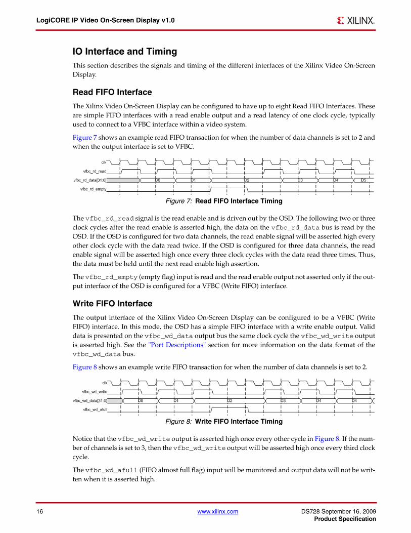
The Xilinx Video On-Screen Display can be configured to have up to eight Read FIFO Interfaces. Theseare simple FIFO interfaces with a read enable output and a read latency of one clock cycle, typicallyused to connect to a VFBC interface within a video system.
Figure 7 shows an example read FIFO transaction for when the number of data channels is set to 2 andwhen the output interface is set to VFBC.
The vfbc_rd_read signal is the read enable and is driven out by the OSD. The following two or threeclock cycles after the read enable is asserted high, the data on the vfbc_rd_data bus is read by theOSD. If the OSD is configured for two data channels, the read enable signal will be asserted high everyother clock cycle with the data read twice. If the OSD is configured for three data channels, the readenable signal will be asserted high once every three clock cycles with the data read three times. Thus,the data must be held until the next read enable high assertion.
The vfbc_rd_empty (empty flag) input is read and the read enable output not asserted only if the out-put interface of the OSD is configured for a VFBC (Write FIFO) interface.
Write FIFO Interface
The output interface of the Xilinx Video On-Screen Display can be configured to be a VFBC (WriteFIFO) interface. In this mode, the OSD has a simple FIFO interface with a write enable output. Validdata is presented on the vfbc_wd_data output bus the same clock cycle the vfbc_wd_write outputis asserted high. See the "Port Descriptions" section for more information on the data format of thevfbc_wd_data bus.
Figure 8 shows an example write FIFO transaction for when the number of data channels is set to 2.
Notice that the vfbc_wd_write output is asserted high once every other cycle in Figure 8. If the num-ber of channels is set to 3, then the vfbc_wd_write output will be asserted high once every third clockcycle.
The vfbc_wd_afull (FIFO almost full flag) input will be monitored and output data will not be writ-ten when it is asserted high.
X-Ref Target - Figure 7
Figure 7: Read FIFO Interface Timing
X-Ref Target - Figure 8
Figure 8: Write FIFO Interface Timing
DS728 September 16, 2009 www.xilinx.com 17Product Specification
LogiCORE IP Video On-Screen Display v1.0
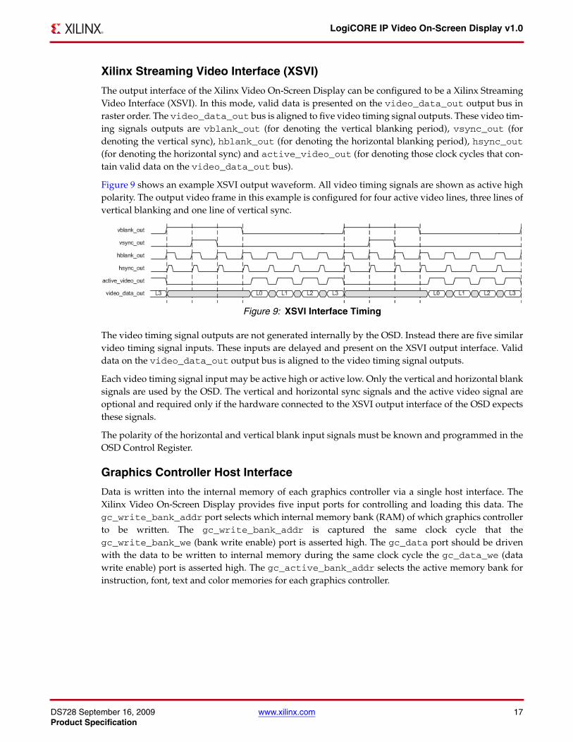
Xilinx Streaming Video Interface (XSVI)
The output interface of the Xilinx Video On-Screen Display can be configured to be a Xilinx StreamingVideo Interface (XSVI). In this mode, valid data is presented on the video_data_out output bus inraster order. The video_data_out bus is aligned to five video timing signal outputs. These video tim-ing signals outputs are vblank_out (for denoting the vertical blanking period), vsync_out (fordenoting the vertical sync), hblank_out (for denoting the horizontal blanking period), hsync_out(for denoting the horizontal sync) and active_video_out (for denoting those clock cycles that con-tain valid data on the video_data_out bus).
Figure 9 shows an example XSVI output waveform. All video timing signals are shown as active highpolarity. The output video frame in this example is configured for four active video lines, three lines ofvertical blanking and one line of vertical sync.
The video timing signal outputs are not generated internally by the OSD. Instead there are five similarvideo timing signal inputs. These inputs are delayed and present on the XSVI output interface. Validdata on the video_data_out output bus is aligned to the video timing signal outputs.
Each video timing signal input may be active high or active low. Only the vertical and horizontal blanksignals are used by the OSD. The vertical and horizontal sync signals and the active video signal areoptional and required only if the hardware connected to the XSVI output interface of the OSD expectsthese signals.
The polarity of the horizontal and vertical blank input signals must be known and programmed in theOSD Control Register.
Graphics Controller Host Interface
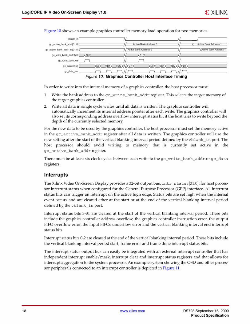
Data is written into the internal memory of each graphics controller via a single host interface. TheXilinx Video On-Screen Display provides five input ports for controlling and loading this data. Thegc_write_bank_addr port selects which internal memory bank (RAM) of which graphics controllerto be written. The gc_write_bank_addr is captured the same clock cycle that thegc_write_bank_we (bank write enable) port is asserted high. The gc_data port should be drivenwith the data to be written to internal memory during the same clock cycle the gc_data_we (datawrite enable) port is asserted high. The gc_active_bank_addr selects the active memory bank forinstruction, font, text and color memories for each graphics controller.
X-Ref Target - Figure 9
Figure 9: XSVI Interface Timing
LogiCORE IP Video On-Screen Display v1.0
18 www.xilinx.com DS728 September 16, 2009Product Specification
Figure 10 shows an example graphics controller memory load operation for two memories.
In order to write into the internal memory of a graphics controller, the host processor must:
1. Write the bank address to the gc_write_bank_addr register. This selects the target memory of the target graphics controller.
2. Write all data in single cycle writes until all data is written. The graphics controller will automatically increment its internal address pointer after each write. The graphics controller will also set its corresponding address overflow interrupt status bit if the host tries to write beyond the depth of the currently selected memory.
For the new data to be used by the graphics controller, the host processor must set the memory activein the gc_active_bank_addr register after all data is written. The graphics controller will use thenew setting after the start of the vertical blanking interval period defined by the vblank_in port. Thehost processor should avoid writing to memory that is currently set active in thegc_active_bank_addr register.
There must be at least six clock cycles between each write to the gc_write_bank_addr or gc_dataregisters.
Interrupts
The Xilinx Video On-Screen Display provides a 32-bit output bus, intr_status[31:0], for host proces-sor interrupt status when configured for the General Purpose Processor (GPP) interface. All interruptstatus bits can trigger an interrupt on the active high edge. Status bits are set high when the internalevent occurs and are cleared ether at the start or at the end of the vertical blanking interval perioddefined by the vblank_in port.
Interrupt status bits 3-31 are cleared at the start of the vertical blanking interval period. These bitsinclude the graphics controller address overflow, the graphics controller instruction error, the outputFIFO overflow error, the input FIFOs underflow error and the vertical blanking interval end interruptstatus bits.
Interrupt status bits 0-2 are cleared at the end of the vertical blanking interval period. These bits includethe vertical blanking interval period start, frame error and frame done interrupt status bits.
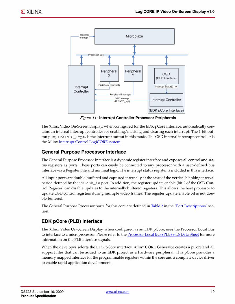
The interrupt status output bus can easily be integrated with an external interrupt controller that hasindependent interrupt enable/mask, interrupt clear and interrupt status registers and that allows forinterrupt aggregation to the system processor. An example system showing the OSD and other proces-sor peripherals connected to an interrupt controller is depicted in Figure 11.
X-Ref Target - Figure 10
Figure 10: Graphics Controller Host Interface Timing
DS728 September 16, 2009 www.xilinx.com 19Product Specification
LogiCORE IP Video On-Screen Display v1.0
The Xilinx Video On-Screen Display, when configured for the EDK pCore Interface, automatically con-tains an internal interrupt controller for enabling/masking and clearing each interrupt. The 1-bit out-put port, IP2INTC_Irpt, is the interrupt output in this mode. The OSD internal interrupt controller isthe Xilinx Interrupt Control LogiCORE system.
General Purpose Processor Interface
The General Purpose Processor Interface is a dynamic register interface and exposes all control and sta-tus registers as ports. These ports can easily be connected to any processor with a user-defined businterface via a Register File and minimal logic. The interrupt status register is included in this interface.
All input ports are double-buffered and captured internally at the start of the vertical blanking intervalperiod defined by the vblank_in port. In addition, the register update enable (bit 2 of the OSD Con-trol Register) can disable updates to the internally buffered registers. This allows the host processor toupdate OSD control registers during multiple video frames. The register update enable bit is not dou-ble-buffered.
The General Purpose Processor ports for this core are defined in Table 2 in the "Port Descriptions" sec-tion.
EDK pCore (PLB) Interface
The Xilinx Video On-Screen Display, when configured as an EDK pCore, uses the Processor Local Busto interface to a microprocessor. Please refer to the Processor Local Bus (PLB) v4.6 Data Sheet for moreinformation on the PLB interface signals.
When the developer selects the EDK pCore interface, Xilinx CORE Generator creates a pCore and allsupport files that can be added to an EDK project as a hardware peripheral. This pCore provides amemory mapped interface for the programmable registers within the core and a complete device driverto enable rapid application development.
X-Ref Target - Figure 11
Figure 11: Interrupt Controller Processor Peripherals

LogiCORE IP Video On-Screen Display v1.0
20 www.xilinx.com DS728 September 16, 2009Product Specification
Xilinx CORE Generator will place all EDK pCore source files in the “pcores” subdirectory located in thecore output directory. The core output directory is given the same name as the component. For exam-ple, if the component name is set to “v_osd_v1_0_u0,” then the EDK pCore source files will be locatedin the following directory:
<coregen project directory>/v_osd_v1_0_u0/pcores/osd_v1_00_a
The pCore should be copied to the user's <EDK_Project>/pcores directory or to a user pCores reposi-tory.
Parameter Modification in CORE Generator
All parameters may be modified in the Xilinx CORE Generator GUI. Modification of these parameterschanges the defaults in the .mpd file: osd_v1_00_a/data/osd_v2_1_0.mpd. This provides the user withan alternative to modifying the parameters in the MHS file in the EDK project. The parameter changesdo not get copied into any MHS file. When migrating EDK projects from one place to another, the MPDfiles for cores modified in this way must also be provided in addition to EDK project files such as theMHS file. Xilinx recommends that all parameter changes be made in the EDK environment.
pCore Device Driver
The Xilinx On-Screen Display pCore includes a software driver written in the C Language that the usercan use to control the Xilinx OSD devices. A high-level API is provided and can be used withoutdetailed knowledge of the Xilinx OSD devices. Application developers are encouraged to use this APIto access the device features. A low-level API is also provided in case applications prefer to access thedevices directly through the system registers described in the previous section.
Table 3 lists the files that are included with the Xilinx OSD pCore driver and their description.
Xilinx CORE Generator software will place all EDK pCore driver files in the “drivers” subdirectorylocated in the core output directory. The core output directory is given the same name as the compo-nent. For example, if the component name is set to “v_osd_v1_0_u0,” then the device driver source fileswill be located in the following directory:
<coregen project directory>/v_osd_v1_0_u0/drivers/osd_v1_00_b/
The driver software should be copied to the user's <EDK_Project>/drivers directory or to a userpCores repository,
Table 3: Device Driver Source Files
File Name Description
xosd.h Contains all prototypes of high-level API to access all of the features of the Xilinx OSD devices.
xosd.c Contains the implementation of high-level API to access all of the features of the Xilinx OSD devices except interrupts.
xosd_intr.c Contains the implementation of high-level API to access interrupt feature of the Xilinx OSD devices.
xosd_sinit.c Contains static initialization methods for the Xilinx OSD device driver.
xosd_g.c Contains a template for configuration table of Xilinx OSD devices. This file is used by the high-level API and will be automatically generated to match the OSD device configurations by Xilinx EDK/SDK tools when the software project is built.
xosd_hw.h Contains Low-level API (that is, register offset/bit definition and register-level driver API) that can be used to access the Xilinx OSD devices.
example.c An example that demonstrates how to control the Xilinx OSD devices using the high-level API.
DS728 September 16, 2009 www.xilinx.com 21Product Specification
LogiCORE IP Video On-Screen Display v1.0
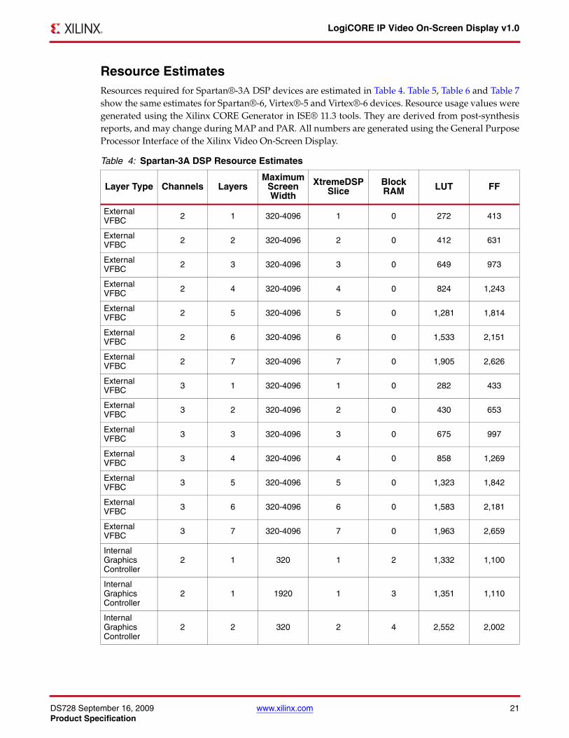
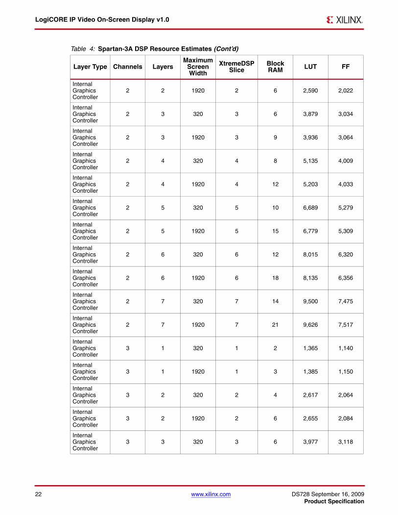
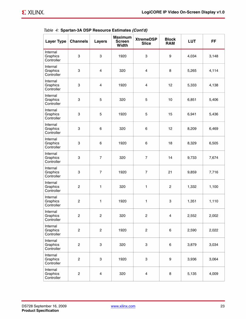
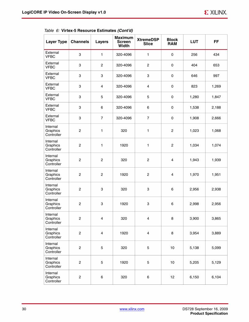
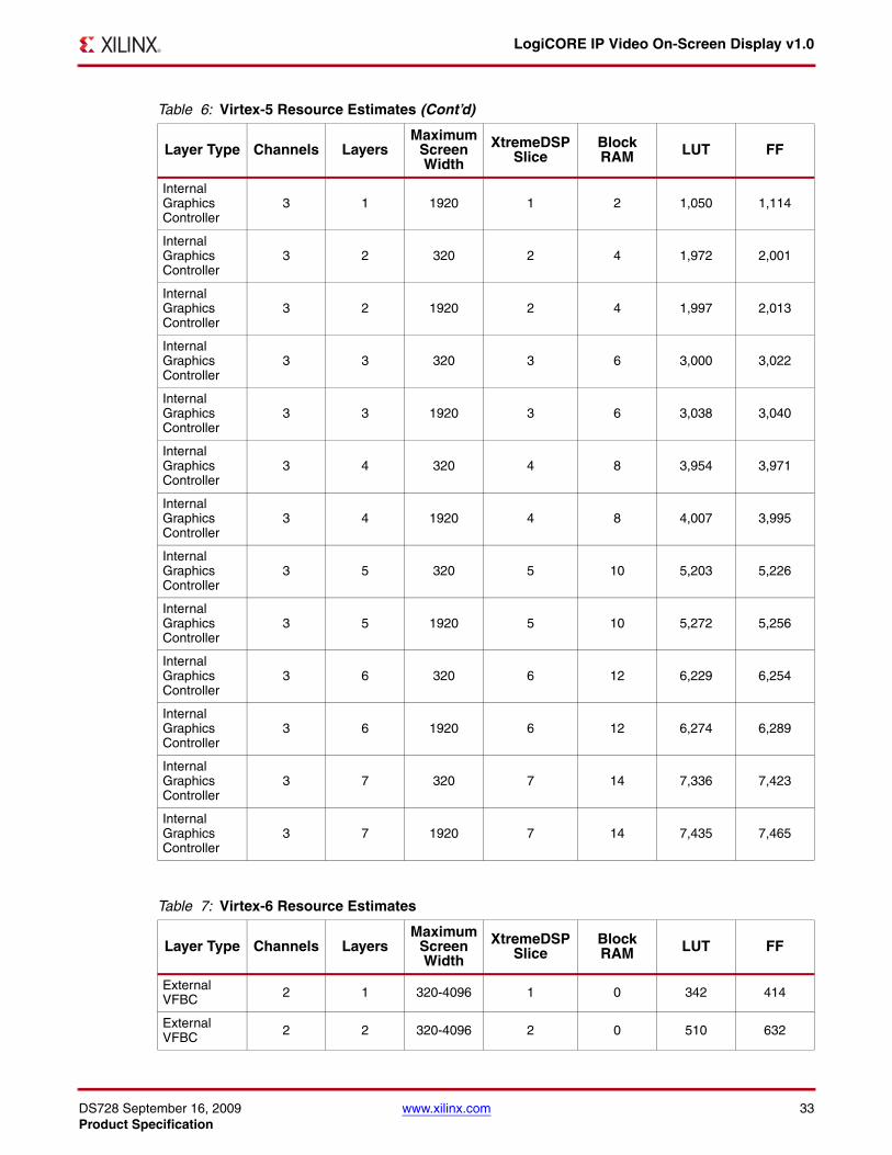
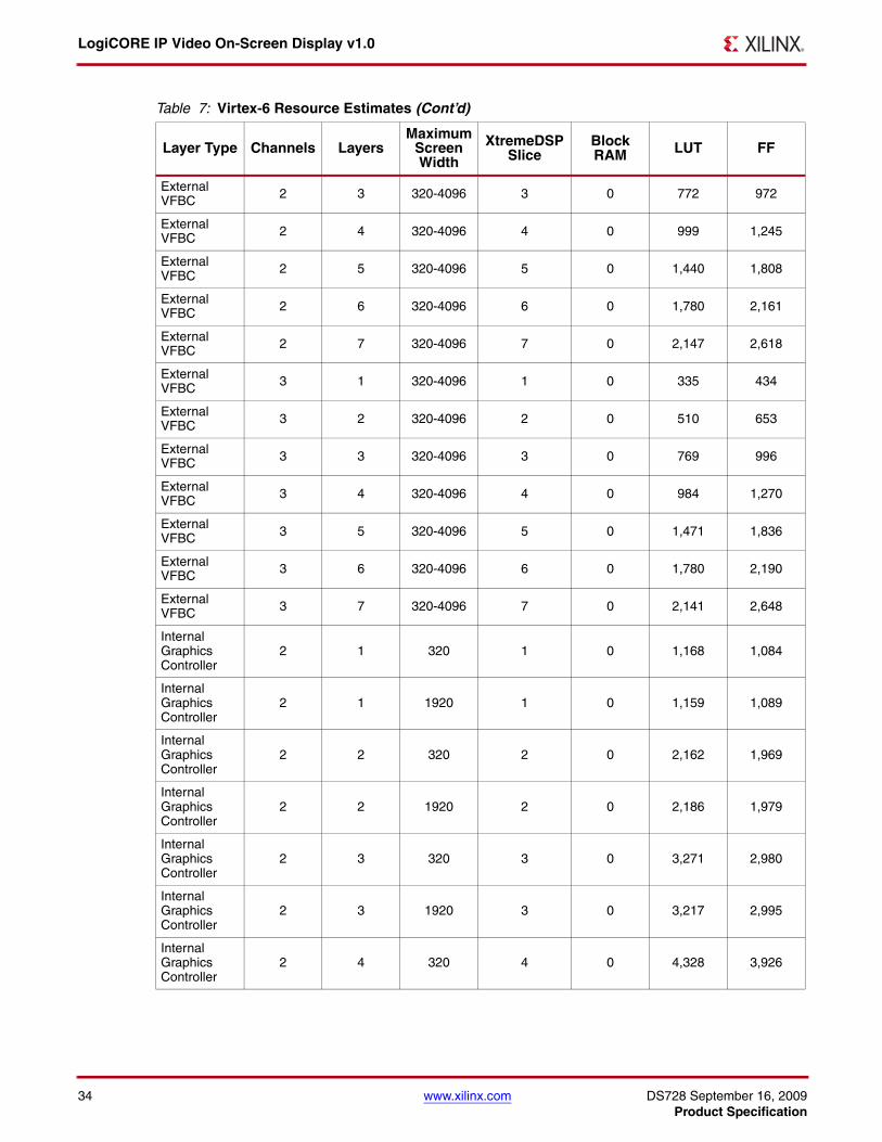
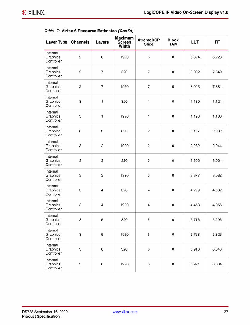
Resource EstimatesResources required for Spartan®-3A DSP devices are estimated in Table 4. Table 5, Table 6 and Table 7show the same estimates for Spartan®-6, Virtex®-5 and Virtex®-6 devices. Resource usage values weregenerated using the Xilinx CORE Generator in ISE® 11.3 tools. They are derived from post-synthesisreports, and may change during MAP and PAR. All numbers are generated using the General PurposeProcessor Interface of the Xilinx Video On-Screen Display.
Table 4: Spartan-3A DSP Resource Estimates
Layer Type Channels LayersMaximum
Screen Width
XtremeDSP Slice
Block RAM LUT FF
External VFBC 2 1 320-4096 1 0 272 413
External VFBC 2 2 320-4096 2 0 412 631
External VFBC 2 3 320-4096 3 0 649 973
External VFBC 2 4 320-4096 4 0 824 1,243
External VFBC 2 5 320-4096 5 0 1,281 1,814
External VFBC 2 6 320-4096 6 0 1,533 2,151
External VFBC 2 7 320-4096 7 0 1,905 2,626
External VFBC 3 1 320-4096 1 0 282 433
External VFBC 3 2 320-4096 2 0 430 653
External VFBC 3 3 320-4096 3 0 675 997
External VFBC 3 4 320-4096 4 0 858 1,269
External VFBC 3 5 320-4096 5 0 1,323 1,842
External VFBC 3 6 320-4096 6 0 1,583 2,181
External VFBC 3 7 320-4096 7 0 1,963 2,659
Internal Graphics Controller
2 1 320 1 2 1,332 1,100
Internal Graphics Controller
2 1 1920 1 3 1,351 1,110
Internal Graphics Controller
2 2 320 2 4 2,552 2,002
LogiCORE IP Video On-Screen Display v1.0
22 www.xilinx.com DS728 September 16, 2009Product Specification
Internal Graphics Controller
2 2 1920 2 6 2,590 2,022
Internal Graphics Controller
2 3 320 3 6 3,879 3,034
Internal Graphics Controller
2 3 1920 3 9 3,936 3,064
Internal Graphics Controller
2 4 320 4 8 5,135 4,009
Internal Graphics Controller
2 4 1920 4 12 5,203 4,033
Internal Graphics Controller
2 5 320 5 10 6,689 5,279
Internal Graphics Controller
2 5 1920 5 15 6,779 5,309
Internal Graphics Controller
2 6 320 6 12 8,015 6,320
Internal Graphics Controller
2 6 1920 6 18 8,135 6,356
Internal Graphics Controller
2 7 320 7 14 9,500 7,475
Internal Graphics Controller
2 7 1920 7 21 9,626 7,517
Internal Graphics Controller
3 1 320 1 2 1,365 1,140
Internal Graphics Controller
3 1 1920 1 3 1,385 1,150
Internal Graphics Controller
3 2 320 2 4 2,617 2,064
Internal Graphics Controller
3 2 1920 2 6 2,655 2,084
Internal Graphics Controller
3 3 320 3 6 3,977 3,118
Table 4: Spartan-3A DSP Resource Estimates (Cont’d)
Layer Type Channels LayersMaximum
Screen Width
XtremeDSP Slice
Block RAM LUT FF
DS728 September 16, 2009 www.xilinx.com 23Product Specification
LogiCORE IP Video On-Screen Display v1.0
Internal Graphics Controller
3 3 1920 3 9 4,034 3,148
Internal Graphics Controller
3 4 320 4 8 5,265 4,114
Internal Graphics Controller
3 4 1920 4 12 5,333 4,138
Internal Graphics Controller
3 5 320 5 10 6,851 5,406
Internal Graphics Controller
3 5 1920 5 15 6,941 5,436
Internal Graphics Controller
3 6 320 6 12 8,209 6,469
Internal Graphics Controller
3 6 1920 6 18 8,329 6,505
Internal Graphics Controller
3 7 320 7 14 9,733 7,674
Internal Graphics Controller
3 7 1920 7 21 9,859 7,716
Internal Graphics Controller
2 1 320 1 2 1,332 1,100
Internal Graphics Controller
2 1 1920 1 3 1,351 1,110
Internal Graphics Controller
2 2 320 2 4 2,552 2,002
Internal Graphics Controller
2 2 1920 2 6 2,590 2,022
Internal Graphics Controller
2 3 320 3 6 3,879 3,034
Internal Graphics Controller
2 3 1920 3 9 3,936 3,064
Internal Graphics Controller
2 4 320 4 8 5,135 4,009
Table 4: Spartan-3A DSP Resource Estimates (Cont’d)
Layer Type Channels LayersMaximum
Screen Width
XtremeDSP Slice
Block RAM LUT FF

LogiCORE IP Video On-Screen Display v1.0
24 www.xilinx.com DS728 September 16, 2009Product Specification
Internal Graphics Controller
2 4 1920 4 12 5,203 4,033
Internal Graphics Controller
2 5 320 5 10 6,689 5,279
Internal Graphics Controller
2 5 1920 5 15 6,779 5,309
Internal Graphics Controller
2 6 320 6 12 8,015 6,320
Internal Graphics Controller
2 6 1920 6 18 8,135 6,356
Internal Graphics Controller
2 7 320 7 14 9,500 7,475
Internal Graphics Controller
2 7 1920 7 21 9,626 7,517
Internal Graphics Controller
3 1 320 1 2 1,365 1,140
Internal Graphics Controller
3 1 1920 1 3 1,385 1,150
Internal Graphics Controller
3 2 320 2 4 2,617 2,064
Internal Graphics Controller
3 2 1920 2 6 2,655 2,084
Internal Graphics Controller
3 3 320 3 6 3,977 3,118
Internal Graphics Controller
3 3 1920 3 9 4,034 3,148
Internal Graphics Controller
3 4 320 4 8 5,265 4,114
Internal Graphics Controller
3 4 1920 4 12 5,333 4,138
Internal Graphics Controller
3 5 320 5 10 6,851 5,406
Table 4: Spartan-3A DSP Resource Estimates (Cont’d)
Layer Type Channels LayersMaximum
Screen Width
XtremeDSP Slice
Block RAM LUT FF

DS728 September 16, 2009 www.xilinx.com 25Product Specification
LogiCORE IP Video On-Screen Display v1.0
Internal Graphics Controller
3 5 1920 5 15 6,941 5,436
Internal Graphics Controller
3 6 320 6 12 8,209 6,469
Internal Graphics Controller
3 6 1920 6 18 8,329 6,505
Internal Graphics Controller
3 7 320 7 14 9,733 7,674
Internal Graphics Controller
3 7 1920 7 21 9,859 7,716
Table 5: Spartan-6 Resource Estimates
Layer Type Channels LayersMaximum
Screen Width
XtremeDSP Slice
Block RAM LUT FF
External VFBC 2 1 320-4096 1 0 319 414
External VFBC 2 2 320-4096 2 0 481 631
External VFBC 2 3 320-4096 3 0 710 971
External VFBC 2 4 320-4096 4 0 896 1,244
External VFBC 2 5 320-4096 5 0 1,222 1,806
External VFBC 2 6 320-4096 6 0 1,539 2,160
External VFBC 2 7 320-4096 7 0 1,736 2,617
External VFBC 3 1 320-4096 1 0 350 434
External VFBC 3 2 320-4096 2 0 503 653
External VFBC 3 3 320-4096 3 0 734 995
External VFBC 3 4 320-4096 4 0 933 1,270
External VFBC 3 5 320-4096 5 0 1,314 1,834
External VFBC 3 6 320-4096 6 0 1,555 2,190
Table 4: Spartan-3A DSP Resource Estimates (Cont’d)
Layer Type Channels LayersMaximum
Screen Width
XtremeDSP Slice
Block RAM LUT FF

LogiCORE IP Video On-Screen Display v1.0
26 www.xilinx.com DS728 September 16, 2009Product Specification
External VFBC 3 7 320-4096 7 0 1,876 2,648
Internal Graphics Controller
2 1 320 1 0 1,071 1,082
Internal Graphics Controller
2 1 1920 1 0 1,106 1,089
Internal Graphics Controller
2 2 320 2 0 1,981 1,967
Internal Graphics Controller
2 2 1920 2 0 2,068 1,981
Internal Graphics Controller
2 3 320 3 0 2,974 2,976
Internal Graphics Controller
2 3 1920 3 0 2,993 2,997
Internal Graphics Controller
2 4 320 4 0 3,990 3,922
Internal Graphics Controller
2 4 1920 4 0 3,778 3,950
Internal Graphics Controller
2 5 320 5 0 5,053 5,163
Internal Graphics Controller
2 5 1920 5 0 5,074 5,197
Internal Graphics Controller
2 6 320 6 0 6,119 6,193
Internal Graphics Controller
2 6 1920 6 0 6,129 6,235
Internal Graphics Controller
2 7 320 7 0 7,028 7,344
Internal Graphics Controller
2 7 1920 7 0 7,238 7,392
Internal Graphics Controller
3 1 320 1 0 1,134 1,122
Table 5: Spartan-6 Resource Estimates (Cont’d)
Layer Type Channels LayersMaximum
Screen Width
XtremeDSP Slice
Block RAM LUT FF

DS728 September 16, 2009 www.xilinx.com 27Product Specification
LogiCORE IP Video On-Screen Display v1.0
Internal Graphics Controller
3 1 1920 1 0 1,094 1,128
Internal Graphics Controller
3 2 320 2 0 2,074 2,029
Internal Graphics Controller
3 2 1920 2 0 2,097 2,041
Internal Graphics Controller
3 3 320 3 0 3,090 3,060
Internal Graphics Controller
3 3 1920 3 0 3,079 3,078
Internal Graphics Controller
3 4 320 4 0 4,052 4,028
Internal Graphics Controller
3 4 1920 4 0 4,100 4,052
Internal Graphics Controller
3 5 320 5 0 5,009 5,290
Internal Graphics Controller
3 5 1920 5 0 5,243 5,320
Internal Graphics Controller
3 6 320 6 0 6,291 6,342
Internal Graphics Controller
3 6 1920 6 0 6,353 6,378
Internal Graphics Controller
3 7 320 7 0 7,242 7,521
Internal Graphics Controller
3 7 1920 7 0 7,470 7,556
Internal Graphics Controller
2 1 320 1 0 1,071 1,082
Internal Graphics Controller
2 1 1920 1 0 1,106 1,089
Internal Graphics Controller
2 2 320 2 0 1,981 1,967
Table 5: Spartan-6 Resource Estimates (Cont’d)
Layer Type Channels LayersMaximum
Screen Width
XtremeDSP Slice
Block RAM LUT FF

LogiCORE IP Video On-Screen Display v1.0
28 www.xilinx.com DS728 September 16, 2009Product Specification
Internal Graphics Controller
2 2 1920 2 0 2,068 1,981
Internal Graphics Controller
2 3 320 3 0 2,974 2,976
Internal Graphics Controller
2 3 1920 3 0 2,993 2,997
Internal Graphics Controller
2 4 320 4 0 3,990 3,922
Internal Graphics Controller
2 4 1920 4 0 3,778 3,950
Internal Graphics Controller
2 5 320 5 0 5,053 5,163
Internal Graphics Controller
2 5 1920 5 0 5,074 5,197
Internal Graphics Controller
2 6 320 6 0 6,119 6,193
Internal Graphics Controller
2 6 1920 6 0 6,129 6,235
Internal Graphics Controller
2 7 320 7 0 7,028 7,344
Internal Graphics Controller
2 7 1920 7 0 7,238 7,392
Internal Graphics Controller
3 1 320 1 0 1,134 1,122
Internal Graphics Controller
3 1 1920 1 0 1,094 1,128
Internal Graphics Controller
3 2 320 2 0 2,074 2,029
Internal Graphics Controller
3 2 1920 2 0 2,097 2,041
Internal Graphics Controller
3 3 320 3 0 3,090 3,060
Table 5: Spartan-6 Resource Estimates (Cont’d)
Layer Type Channels LayersMaximum
Screen Width
XtremeDSP Slice
Block RAM LUT FF

DS728 September 16, 2009 www.xilinx.com 29Product Specification
LogiCORE IP Video On-Screen Display v1.0
Internal Graphics Controller
3 3 1920 3 0 3,079 3,078
Internal Graphics Controller
3 4 320 4 0 4,052 4,028
Internal Graphics Controller
3 4 1920 4 0 4,100 4,052
Internal Graphics Controller
3 5 320 5 0 5,009 5,290
Internal Graphics Controller
3 5 1920 5 0 5,243 5,320
Internal Graphics Controller
3 6 320 6 0 6,291 6,342
Internal Graphics Controller
3 6 1920 6 0 6,353 6,378
Internal Graphics Controller
3 7 320 7 0 7,242 7,521
Internal Graphics Controller
3 7 1920 7 0 7,470 7,556
Table 6: Virtex-5 Resource Estimates
Layer Type Channels LayersMaximum
Screen Width
XtremeDSP Slice
Block RAM LUT FF
External VFBC 2 1 320-4096 1 0 254 414
External VFBC 2 2 320-4096 2 0 401 631
External VFBC 2 3 320-4096 3 0 644 973
External VFBC 2 4 320-4096 4 0 823 1,243
External VFBC 2 5 320-4096 5 0 1,281 1,819
External VFBC 2 6 320-4096 6 0 1,538 2,157
External VFBC 2 7 320-4096 7 0 1,907 2,634
Table 5: Spartan-6 Resource Estimates (Cont’d)
Layer Type Channels LayersMaximum
Screen Width
XtremeDSP Slice
Block RAM LUT FF
LogiCORE IP Video On-Screen Display v1.0
30 www.xilinx.com DS728 September 16, 2009Product Specification
External VFBC 3 1 320-4096 1 0 256 434
External VFBC 3 2 320-4096 2 0 404 653
External VFBC 3 3 320-4096 3 0 646 997
External VFBC 3 4 320-4096 4 0 823 1,269
External VFBC 3 5 320-4096 5 0 1,280 1,847
External VFBC 3 6 320-4096 6 0 1,538 2,188
External VFBC 3 7 320-4096 7 0 1,908 2,666
Internal Graphics Controller
2 1 320 1 2 1,023 1,068
Internal Graphics Controller
2 1 1920 1 2 1,034 1,074
Internal Graphics Controller
2 2 320 2 4 1,943 1,939
Internal Graphics Controller
2 2 1920 2 4 1,970 1,951
Internal Graphics Controller
2 3 320 3 6 2,956 2,938
Internal Graphics Controller
2 3 1920 3 6 2,998 2,956
Internal Graphics Controller
2 4 320 4 8 3,900 3,865
Internal Graphics Controller
2 4 1920 4 8 3,954 3,889
Internal Graphics Controller
2 5 320 5 10 5,138 5,099
Internal Graphics Controller
2 5 1920 5 10 5,205 5,129
Internal Graphics Controller
2 6 320 6 12 6,150 6,104
Table 6: Virtex-5 Resource Estimates (Cont’d)
Layer Type Channels LayersMaximum
Screen Width
XtremeDSP Slice
Block RAM LUT FF

DS728 September 16, 2009 www.xilinx.com 31Product Specification
LogiCORE IP Video On-Screen Display v1.0
Internal Graphics Controller
2 6 1920 6 12 6,233 6,140
Internal Graphics Controller
2 7 320 7 14 7,293 7,252
Internal Graphics Controller
2 7 1920 7 14 7,386 7,294
Internal Graphics Controller
3 1 320 1 2 1,038 1,108
Internal Graphics Controller
3 1 1920 1 2 1,050 1,114
Internal Graphics Controller
3 2 320 2 4 1,972 2,001
Internal Graphics Controller
3 2 1920 2 4 1,997 2,013
Internal Graphics Controller
3 3 320 3 6 3,000 3,022
Internal Graphics Controller
3 3 1920 3 6 3,038 3,040
Internal Graphics Controller
3 4 320 4 8 3,954 3,971
Internal Graphics Controller
3 4 1920 4 8 4,007 3,995
Internal Graphics Controller
3 5 320 5 10 5,203 5,226
Internal Graphics Controller
3 5 1920 5 10 5,272 5,256
Internal Graphics Controller
3 6 320 6 12 6,229 6,254
Internal Graphics Controller
3 6 1920 6 12 6,274 6,289
Internal Graphics Controller
3 7 320 7 14 7,336 7,423
Table 6: Virtex-5 Resource Estimates (Cont’d)
Layer Type Channels LayersMaximum
Screen Width
XtremeDSP Slice
Block RAM LUT FF

LogiCORE IP Video On-Screen Display v1.0
32 www.xilinx.com DS728 September 16, 2009Product Specification
Internal Graphics Controller
3 7 1920 7 14 7,435 7,465
Internal Graphics Controller
2 1 320 1 2 1,023 1,068
Internal Graphics Controller
2 1 1920 1 2 1,034 1,074
Internal Graphics Controller
2 2 320 2 4 1,943 1,939
Internal Graphics Controller
2 2 1920 2 4 1,970 1,951
Internal Graphics Controller
2 3 320 3 6 2,956 2,938
Internal Graphics Controller
2 3 1920 3 6 2,998 2,956
Internal Graphics Controller
2 4 320 4 8 3,900 3,865
Internal Graphics Controller
2 4 1920 4 8 3,954 3,889
Internal Graphics Controller
2 5 320 5 10 5,138 5,099
Internal Graphics Controller
2 5 1920 5 10 5,205 5,129
Internal Graphics Controller
2 6 320 6 12 6,150 6,104
Internal Graphics Controller
2 6 1920 6 12 6,233 6,140
Internal Graphics Controller
2 7 320 7 14 7,293 7,252
Internal Graphics Controller
2 7 1920 7 14 7,386 7,294
Internal Graphics Controller
3 1 320 1 2 1,038 1,108
Table 6: Virtex-5 Resource Estimates (Cont’d)
Layer Type Channels LayersMaximum
Screen Width
XtremeDSP Slice
Block RAM LUT FF
DS728 September 16, 2009 www.xilinx.com 33Product Specification
LogiCORE IP Video On-Screen Display v1.0
Internal Graphics Controller
3 1 1920 1 2 1,050 1,114
Internal Graphics Controller
3 2 320 2 4 1,972 2,001
Internal Graphics Controller
3 2 1920 2 4 1,997 2,013
Internal Graphics Controller
3 3 320 3 6 3,000 3,022
Internal Graphics Controller
3 3 1920 3 6 3,038 3,040
Internal Graphics Controller
3 4 320 4 8 3,954 3,971
Internal Graphics Controller
3 4 1920 4 8 4,007 3,995
Internal Graphics Controller
3 5 320 5 10 5,203 5,226
Internal Graphics Controller
3 5 1920 5 10 5,272 5,256
Internal Graphics Controller
3 6 320 6 12 6,229 6,254
Internal Graphics Controller
3 6 1920 6 12 6,274 6,289
Internal Graphics Controller
3 7 320 7 14 7,336 7,423
Internal Graphics Controller
3 7 1920 7 14 7,435 7,465
Table 7: Virtex-6 Resource Estimates
Layer Type Channels LayersMaximum
Screen Width
XtremeDSP Slice
Block RAM LUT FF
External VFBC 2 1 320-4096 1 0 342 414
External VFBC 2 2 320-4096 2 0 510 632
Table 6: Virtex-5 Resource Estimates (Cont’d)
Layer Type Channels LayersMaximum
Screen Width
XtremeDSP Slice
Block RAM LUT FF
LogiCORE IP Video On-Screen Display v1.0
34 www.xilinx.com DS728 September 16, 2009Product Specification
External VFBC 2 3 320-4096 3 0 772 972
External VFBC 2 4 320-4096 4 0 999 1,245
External VFBC 2 5 320-4096 5 0 1,440 1,808
External VFBC 2 6 320-4096 6 0 1,780 2,161
External VFBC 2 7 320-4096 7 0 2,147 2,618
External VFBC 3 1 320-4096 1 0 335 434
External VFBC 3 2 320-4096 2 0 510 653
External VFBC 3 3 320-4096 3 0 769 996
External VFBC 3 4 320-4096 4 0 984 1,270
External VFBC 3 5 320-4096 5 0 1,471 1,836
External VFBC 3 6 320-4096 6 0 1,780 2,190
External VFBC 3 7 320-4096 7 0 2,141 2,648
Internal Graphics Controller
2 1 320 1 0 1,168 1,084
Internal Graphics Controller
2 1 1920 1 0 1,159 1,089
Internal Graphics Controller
2 2 320 2 0 2,162 1,969
Internal Graphics Controller
2 2 1920 2 0 2,186 1,979
Internal Graphics Controller
2 3 320 3 0 3,271 2,980
Internal Graphics Controller
2 3 1920 3 0 3,217 2,995
Internal Graphics Controller
2 4 320 4 0 4,328 3,926
Table 7: Virtex-6 Resource Estimates (Cont’d)
Layer Type Channels LayersMaximum
Screen Width
XtremeDSP Slice
Block RAM LUT FF

DS728 September 16, 2009 www.xilinx.com 35Product Specification
LogiCORE IP Video On-Screen Display v1.0
Internal Graphics Controller
2 4 1920 4 0 4,353 3,946
Internal Graphics Controller
2 5 320 5 0 5,597 5,167
Internal Graphics Controller
2 5 1920 5 0 5,516 5,192
Internal Graphics Controller
2 6 320 6 0 6,800 6,198
Internal Graphics Controller
2 6 1920 6 0 6,824 6,228
Internal Graphics Controller
2 7 320 7 0 8,002 7,349
Internal Graphics Controller
2 7 1920 7 0 8,043 7,384
Internal Graphics Controller
3 1 320 1 0 1,180 1,124
Internal Graphics Controller
3 1 1920 1 0 1,198 1,130
Internal Graphics Controller
3 2 320 2 0 2,197 2,032
Internal Graphics Controller
3 2 1920 2 0 2,232 2,044
Internal Graphics Controller
3 3 320 3 0 3,306 3,064
Internal Graphics Controller
3 3 1920 3 0 3,377 3,082
Internal Graphics Controller
3 4 320 4 0 4,299 4,032
Internal Graphics Controller
3 4 1920 4 0 4,458 4,056
Internal Graphics Controller
3 5 320 5 0 5,716 5,296
Table 7: Virtex-6 Resource Estimates (Cont’d)
Layer Type Channels LayersMaximum
Screen Width
XtremeDSP Slice
Block RAM LUT FF

LogiCORE IP Video On-Screen Display v1.0
36 www.xilinx.com DS728 September 16, 2009Product Specification
Internal Graphics Controller
3 5 1920 5 0 5,768 5,326
Internal Graphics Controller
3 6 320 6 0 6,918 6,348
Internal Graphics Controller
3 6 1920 6 0 6,991 6,384
Internal Graphics Controller
3 7 320 7 0 8,020 7,521
Internal Graphics Controller
3 7 1920 7 0 8,078 7,563
Internal Graphics Controller
2 1 320 1 0 1,168 1,084
Internal Graphics Controller
2 1 1920 1 0 1,159 1,089
Internal Graphics Controller
2 2 320 2 0 2,162 1,969
Internal Graphics Controller
2 2 1920 2 0 2,186 1,979
Internal Graphics Controller
2 3 320 3 0 3,271 2,980
Internal Graphics Controller
2 3 1920 3 0 3,217 2,995
Internal Graphics Controller
2 4 320 4 0 4,328 3,926
Internal Graphics Controller
2 4 1920 4 0 4,353 3,946
Internal Graphics Controller
2 5 320 5 0 5,597 5,167
Internal Graphics Controller
2 5 1920 5 0 5,516 5,192
Internal Graphics Controller
2 6 320 6 0 6,800 6,198
Table 7: Virtex-6 Resource Estimates (Cont’d)
Layer Type Channels LayersMaximum
Screen Width
XtremeDSP Slice
Block RAM LUT FF
DS728 September 16, 2009 www.xilinx.com 37Product Specification
LogiCORE IP Video On-Screen Display v1.0
Internal Graphics Controller
2 6 1920 6 0 6,824 6,228
Internal Graphics Controller
2 7 320 7 0 8,002 7,349
Internal Graphics Controller
2 7 1920 7 0 8,043 7,384
Internal Graphics Controller
3 1 320 1 0 1,180 1,124
Internal Graphics Controller
3 1 1920 1 0 1,198 1,130
Internal Graphics Controller
3 2 320 2 0 2,197 2,032
Internal Graphics Controller
3 2 1920 2 0 2,232 2,044
Internal Graphics Controller
3 3 320 3 0 3,306 3,064
Internal Graphics Controller
3 3 1920 3 0 3,377 3,082
Internal Graphics Controller
3 4 320 4 0 4,299 4,032
Internal Graphics Controller
3 4 1920 4 0 4,458 4,056
Internal Graphics Controller
3 5 320 5 0 5,716 5,296
Internal Graphics Controller
3 5 1920 5 0 5,768 5,326
Internal Graphics Controller
3 6 320 6 0 6,918 6,348
Internal Graphics Controller
3 6 1920 6 0 6,991 6,384
Table 7: Virtex-6 Resource Estimates (Cont’d)
Layer Type Channels LayersMaximum
Screen Width
XtremeDSP Slice
Block RAM LUT FF
LogiCORE IP Video On-Screen Display v1.0
38 www.xilinx.com DS728 September 16, 2009Product Specification
PerformanceTable 8 lists typical clock frequencies for the target families.The maximum achievable clock frequencycould vary and in most cases will be higher. The maximum achievable clock frequency and all resourcecounts may be affected by other tool options, additional logic in the FPGA device, using a different ver-sion of Xilinx tools, and other factors.
Support Xilinx provides technical support for this LogiCORE product when used as described in the productdocumentation. Xilinx cannot guarantee timing, functionality, or support of product if implemented indevices that are not defined in the documentation, if customized beyond that allowed in the productdocumentation, or if changes are made to any section of the design labeled DO NOT MODIFY.
Licensing OptionsThe Xilinx Video On-Screen Display LogiCORE system provides three licensing options. After install-ing the required Xilinx ISE software and IP Service Packs, choose a license option.
Simulation Only
The Simulation Only Evaluation license key is provided with the Xilinx CORE Generator tool. This keylets you assess the core functionality with either the provided example design or alongside your owndesign and demonstrates the various interfaces on the core in simulation. (Functional simulation issupported by a dynamically-generated HDL structural model.)
Internal Graphics Controller
3 7 320 7 0 8,020 7,521
Internal Graphics Controller
3 7 1920 7 0 8,078 7,563
Table 8: Target Family Clock Frequencies
Device Family Maximum Clock Frequency (FMax)
For Virtex-6 devices 225 MHz
For Spartan6 devices 150 MHz
For Virtex-5 devices 225MHz
For Spartan-3A DSP devices 150 MHz
Table 7: Virtex-6 Resource Estimates (Cont’d)
Layer Type Channels LayersMaximum
Screen Width
XtremeDSP Slice
Block RAM LUT FF
DS728 September 16, 2009 www.xilinx.com 39Product Specification
LogiCORE IP Video On-Screen Display v1.0
Full System Hardware Evaluation
The Full System Hardware Evaluation license is available at no cost and lets you fully integrate the coreinto an FPGA design, place and route the design, evaluate timing, and perform back-annotatedgatelevel simulation of the core using the demonstration test bench provided with the core.
In addition, the license key lets you generate a bitstream from the placed and routed design, which canthen be downloaded to a supported device and tested in hardware. The core can be tested in the targetdevice for a limited time before timing out (ceasing to function), at which time it can be reactivated byreconfiguring the device. This core is configured to timeout after 8 hours of operation.
Full
The Full license key is provided when you purchase the core and provides full access to all core func-tionality both in simulation and in hardware, including:
• Functional simulation support
• Back annotated gate-level simulation support
• Full implementation support including place and route and bitstream generation
• Full functionality in the programmed device with no time outs
Obtaining Your LicenseThis section contains information about obtaining a simulation, full system hardware, and full licensekeys.
Simulation License
No action is required to obtain the Simulation Only Evaluation license key; it is provided by defaultwith the Xilinx CORE Generator software.
Full System hardware Evaluation License1. Navigate to the product page for this core.
2. Click Evaluate.
3. Follow the instructions to install the required Xilinx ISE software and IP Service Packs.
Obtaining a Full License
To obtain a Full license key, purchase a license for the core. After doing so, click the “Access Core” linkon the Xilinx.com IP core product page for further instructions.
Installing Your License File
The Simulation Only Evaluation license key is provided with the ISE CORE Generator system and doesnot require installation of an additional license file. For the Full System Hardware Evaluation licenseand the Full license, an email will be sent to you containing instructions for installing your license file.Additional details about IP license key installation can be found in the ISE Design Suite Installation,Licensing and Release Notes document.

LogiCORE IP Video On-Screen Display v1.0
40 www.xilinx.com DS728 September 16, 2009Product Specification
Ordering InformationThe Xilinx Video On-Screen Display v1.0 core is provided under the SignOnce IP Site License and canbe generated using the Xilinx CORE Generator system v11.3 or higher. The CORE Generator system isshipped with Xilinx ISE Foundation Series Development software.
A simulation evaluation license for the core is shipped with the CORE Generator system. To access thefull functionality of the core, including FPGA bitstream generation, a full license must be obtained fromXilinx. For more information, please visit the product page for this core.
Please contact your local Xilinx sales representative for pricing and availability of additional XilinxLogiCORE modules and software. Information about additional Xilinx LogiCORE modules is availableon the Xilinx IP Center.
Revision HistoryThe following table shows the revision history for this document:
Notice of DisclaimerXilinx is providing this product documentation, hereinafter “Information,” to you “AS IS” with no warranty of anykind, express or implied. Xilinx makes no representation that the Information, or any particular implementationthereof, is free from any claims of infringement. You are responsible for obtaining any rights you may require forany implementation based on the Information. All specifications are subject to change without notice. XILINXEXPRESSLY DISCLAIMS ANY WARRANTY WHATSOEVER WITH RESPECT TO THE ADEQUACY OF THEINFORMATION OR ANY IMPLEMENTATION BASED THEREON, INCLUDING BUT NOT LIMITED TO ANYWARRANTIES OR REPRESENTATIONS THAT THIS IMPLEMENTATION IS FREE FROM CLAIMS OFINFRINGEMENT AND ANY IMPLIED WARRANTIES OF MERCHANTABILITY OR FITNESS FOR APARTICULAR PURPOSE. Except as stated herein, none of the Information may be copied, reproduced,distributed, republished, downloaded, displayed, posted, or transmitted in any form or by any means including,but not limited to, electronic, mechanical, photocopying, recording, or otherwise, without the prior written consentof Xilinx.
Date Version Description of Revisions
09/16/09 1.0 Initial Xilinx release.