LogiCORE IP MII to RMII (v1.01.a) - Xilinx MII to RMII core accepts the 16 signal MII interface and...
12
DS476 July 25, 2012 www.xilinx.com 1 Product Specification © Copyright 2003–2006, 2008–2012 Xilinx, Inc. Xilinx, the Xilinx logo, Artix, ISE, Kintex, Spartan, Virtex, Vivado, Zynq, and other designated brands included herein are trademarks of Xilinx in the United States and other countries. All other trademarks are the property of their respective owners. Introduction The Xilinx ® LogiCORE™ IP Media Independent Interface (MII) to Reduced Media Independent (RMII) design provides the RMII between RMII-compliant ethernet physical media devices (PHY) and Xilinx 10/100 Mb/s ethernet cores such as the XPS LL TEMAC and XPS Ethernet Lite. These cores provide the traditional MII that requires 16 signals to communicate with an ethernet PHY. The MII to RMII core accepts the 16 signal MII interface and provides a six or seven signal interface to an RMII compliant PHY. Additionally, a fixed 50 MHz reference clock synchronizes the MII to RMII core with both interfaces. The 50 MHz reference clock can be provided by a source external to the host FPGA, or generated within the host FPGA. The MII to RMII core follows the specification defined by the RMII Consortium (version 1.0). Features The MII to RMII core is a soft IP core designed for Xilinx ® FPGAs and contains these features: • Core design is based on RMII specification 1.0 • Parameter to allow automatic detection of receive throughput (transmit side always fixed throughput) • Parameter to select fixed throughput of 10 or 100 Mbits per second • Fixed clock frequency of 50 MHz LogiCORE IP MII to RMII (v1.01.a) DS476 July 25, 2012 Product Specification LogiCORE IP Facts Table Core Specifics Supported Device Family (1) Zynq™-7000 (2) , Virtex ® -7, Kintex™-7, Artix™-7, Virtex-6, Spartan ® -6, Virtex-5, Virtex-4, Spartan-3, Spartan-3A, Spartan-3E Supported User Interfaces N/A Resources See Table 3 through Table 7 Provided with Core Design Files ISE ® : VHDL Vivado™: RTL Example Design Not Provided Test Bench VHDL Test Bench Constraints File None Simulation Model None Supported S/W Driver N/A Tested Design Flows (3) Design Entry Platform Studio (XPS) Vivado Design Suite (4) Simulation Mentor Graphic ModelSim Synthesis Xilinx Synthesis Technology (XST) Vivado Synthesis Support Provided by Xilinx @ www.xilinx.com/support Notes: 1. For a complete list of supported derivative devices, see the Embedded Edition Derivative Device Support . 2. Supported in ISE Design Suite implementations only. 3. For the supported versions of the tools, see the Xilinx Design Tools: Release Notes Guide . 4. Supports only 7 series devices.
Transcript of LogiCORE IP MII to RMII (v1.01.a) - Xilinx MII to RMII core accepts the 16 signal MII interface and...

DS476 July 25, 2012 www.xilinx.com 1Product Specification
© Copyright 2003–2006, 2008–2012 Xilinx, Inc. Xilinx, the Xilinx logo, Artix, ISE, Kintex, Spartan, Virtex, Vivado, Zynq, and other designated brands included herein are trademarks of Xilinx in the United States and other countries. All other trademarks are the property of their respective owners.
a
IntroductionThe Xilinx® LogiCORE™ IP Media IndependentInterface (MII) to Reduced Media Independent (RMII)design provides the RMII between RMII-compliantethernet physical media devices (PHY) and Xilinx10/100 Mb/s ethernet cores such as the XPS LLTEMAC and XPS Ethernet Lite. These cores provide thetraditional MII that requires 16 signals to communicatewith an ethernet PHY. The MII to RMII core accepts the16 signal MII interface and provides a six or sevensignal interface to an RMII compliant PHY.Additionally, a fixed 50 MHz reference clocksynchronizes the MII to RMII core with both interfaces.The 50 MHz reference clock can be provided by asource external to the host FPGA, or generated withinthe host FPGA. The MII to RMII core follows thespecification defined by the RMII Consortium(version 1.0).
FeaturesThe MII to RMII core is a soft IP core designed forXilinx® FPGAs and contains these features:
• Core design is based on RMII specification 1.0
• Parameter to allow automatic detection of receive throughput (transmit side always fixed throughput)
• Parameter to select fixed throughput of 10 or 100 Mbits per second
• Fixed clock frequency of 50 MHz
LogiCORE IP MII to RMII (v1.01.a)
DS476 July 25, 2012 Product Specification
LogiCORE IP Facts Table
Core Specifics
Supported Device Family(1)
Zynq™-7000(2), Virtex®-7, Kintex™-7, Artix™-7,Virtex-6, Spartan®-6, Virtex-5, Virtex-4,
Spartan-3, Spartan-3A, Spartan-3E
Supported User Interfaces N/A
Resources See Table 3 through Table 7
Provided with Core
Design Files ISE®: VHDLVivado™: RTL
Example Design Not Provided
Test Bench VHDL Test Bench
Constraints File None
Simulation Model None
Supported S/W Driver N/A
Tested Design Flows(3)
Design Entry Platform Studio (XPS)Vivado Design Suite(4)
Simulation Mentor Graphic ModelSim
Synthesis Xilinx Synthesis Technology (XST)Vivado Synthesis
Support
Provided by Xilinx @ www.xilinx.com/support
Notes: 1. For a complete list of supported derivative devices, see the
Embedded Edition Derivative Device Support.2. Supported in ISE Design Suite implementations only.3. For the supported versions of the tools, see the Xilinx
Design Tools: Release Notes Guide.4. Supports only 7 series devices.

DS476 July 25, 2012 www.xilinx.com 2Product Specification
LogiCORE IP MII to RMII (v1.01.a)
Functional DescriptionThe block diagram for the MII to RMII core is shown in Figure 1. This diagram shows the usage, location, andconnections for the MII to RMII core. The Ref_Clk must be provided to clock the MII to RMII core internal to thehost FPGA and external to clock the PHY. The clock can be generated either external to, or within the host FPGA, aslong as provisions are made to clock all of the necessary blocks.
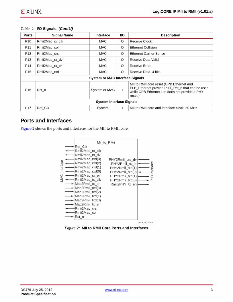
I/O SignalsThe I/O signals for the MII to RMII core are listed in Table 1. The interfaces referenced in this table are shown inFigure 2 in the MII to RMII core usage diagram.
X-Ref Target - Figure 1
Figure 1: MII to RMII Core Usage Block Diagram
Table 1: I/O Signals
Ports Signal Name Interface I/O Description
RMII PHY Interface Signals
P1 Phy2Rmii_crs_dv PHY I Carrier Sense / Data Valid
P2 Phy2Rmii_rx_er PHY I Receive Error (optional)
P3 Phy2Rmii_rxd PHY I Receive Data, 2 bits
P4 Rmii2Phy_txd PHY O Transmit Data, 2 bits
P5 Rmii2Phy_tx_en PHY O Transmit Enable
Ethernet MAC Interface Signals
P6 Mac2Rmii_tx_en MAC I Transmit Enable
P7 Mac2Rmii_txd MAC I Transmit Data, 4 bits
P8 Mac2Rmii_tx_er MAC I Transmit Error
P9 Rmii2Mac_tx_clk MAC O Transmit Clock
PHY_rx_clk PHY_dv
PHY_rx_data PHY_rx_er
PHY_tx_clk PHY_tx_en
PHY_tx_data PHY_tx_er
PHY_crs PHY_col
PHY_rst_n
PHY2Rmii_crs_dv PHY2Rmii_rx_er
PHY2Rmii_rxd Rmii2PHY_txd
Rmii2PHY_tx_en
Ref_Clk CRS_dv Rx_er Rxd Txd Tx_en Rst_n
MDC
MDIO
PHY_Mii_clk_I PHY_Mii_clk_O
PHY_Mii_clk_T PHY_Mii_data_I
PHY_Mii_data_O
Ref_Clk Rmii2Mac_rx_clk Rmii2Mac_rx_dv Rmii2Mac_rxd Rmii2Mac_rx_er Rmii2Mac_tx_clk Mac2Rmii_tx_en Mac2Rmii_txd Mac2Rmii_tx_er Rmii2Mac_crs Rmii2Mac_col Rst_n
Mii to RMii
Ref_Clk
PHY
EMAC
PHY_Mii_data_T
DS476_01_041910
DS476 July 25, 2012 www.xilinx.com 3Product Specification
LogiCORE IP MII to RMII (v1.01.a)
Ports and InterfacesFigure 2 shows the ports and interfaces for the MII to RMII core.
P10 Rmii2Mac_rx_clk MAC O Receive Clock
P11 Rmii2Mac_col MAC O Ethernet Collision
P12 Rmii2Mac_crs MAC O Ethernet Carrier Sense
P13 Rmii2Mac_rx_dv MAC O Receive Data Valid
P14 Rmii2Mac_rx_er MAC O Receive Error
P15 Rmii2Mac_rxd MAC O Receive Data, 4 bits
System or MAC Interface Signals
P16 Rst_n System or MAC I
MII to RMII core reset (OPB Ethernet and PLB_Ethernet provide PHY_Rst_n that can be used while OPB Ethernet Lite does not provide a PHY reset.)
System Interface Signals
P17 Ref_Clk System I MII to RMII core and interface clock, 50 MHz
X-Ref Target - Figure 2
Figure 2: MII to RMII Core Ports and Interfaces
Table 1: I/O Signals (Cont’d)
Ports Signal Name Interface I/O Description
PHY2Rmii_crs_dv PHY2Rmii_rx_er
PHY2Rmii_rxd(1) PHY2Rmii_rxd(0) PHY2Rmii_txd(1) PHY2Rmii_txd(0) Rmii2PHY_tx_en
Ref_Clk Rmii2Mac_rx_clk Rmii2Mac_rx_dv Rmii2Mac_rxd(3) Rmii2Mac_rxd(2) Rmii2Mac_rxd(1) Rmii2Mac_rxd(0) Rmii2Mac_rx_er Rmii2Mac_tx_clk Mac2Rmii_tx_en Mac2Rmii_txd(3) Mac2Rmii_txd(2) Mac2Rmii_txd(1) Mac2Rmii_txd(0) Mac2Rmii_tx_er Rmii2Mac_crs Rmii2Mac_col Rst_n
Mii_to_RMii
PH
YIn
terf
ace
MA
C In
terf
ace
DS476_01_041910

DS476 July 25, 2012 www.xilinx.com 4Product Specification
LogiCORE IP MII to RMII (v1.01.a)
ParametersTo allow the user to obtain an MII to RMII design that is uniquely tailored for their system, certain features areparameterizable, thereby allowing the user to have a design that only utilizes the resources required by their systemand runs at the best possible performance. The features that are parameterizable in the Xilinx MII to RMII core areshown in Table 2.
Allowable Parameter Combinations
There are no restrictions on parameter combinations in the Xilinx MII to RMII core other than setting the parametersto proper logic values, 0 or 1. The note in Table 2 defines the interaction of the two parameters.
Signal ProtocolsThe diagrams in this section illustrate various signal protocols for the MII to RMII core. The protocols vary fromtransmit to receive, RMII to PHY, PHY to RMII, MII to RMII, RMII to MII, and data rates of 10 or 100 Mb/s(megabits per second). Figure 3 shows a typical transaction between the physical interface, PHY, and RMII interfaceon the receive side operating at 100 Mb/s. Several idle dibits, 2 bits at time, can follow the assertion ofPhy2Rmii_crs_dv and precede the preamble dibits. In this case, the Phy2Rmii_crs_dv remains asserted untilthe final packet dibit.
Table 2: Core Parameters
Generic Feature / Description Parameter Name Allowable Values Default Value VHDL Type
MII to RMII Core Parameters
G1 Fixed ethernet throughput C_FIXED_SPEED (1) 0 = Auto (rec. only)1 = Fixed 1 std_logic
G2 Throughput set at 100 Mb/s C_SPEED_100 0 = 10 Mb/s1 = 100 Mb/s 1 std_logic
Notes: 1. When C_FIXED_SPEED = 0, only the receive side automatically detects ethernet throughput. The transmit side operates at a fixed
throughput that is determined by C_SPEED_100. When C_FIXED_SPEED is set to 1, C_SPEED_100 determines the fixed throughput for both transmit and receive
X-Ref Target - Figure 3
Figure 3: Typical PHY to RMII Receive Transaction at 100 Mbps
DS476_03_041910
00 01 11
Ref_Clk (50 MHz)
0 or moreidle dibits
Packet payload, 4 n dibits, where n is the number of bytes inthe packet, including Src/Dest addresses, data, pad, and FCS.
LastSFDdibit
31 ‘01’ dibits28 preamb.3 for SFD
Phy2Rmii_crs_dv
Phy2Rmii_rxd(1:0)

DS476 July 25, 2012 www.xilinx.com 5Product Specification
LogiCORE IP MII to RMII (v1.01.a)
Figure 4 shows another 100 Mb/s PHY to RMII receive transaction. However, in this case Phy2Rmii_crs_dv
deasserts on the boundary of the last nibble, where two dibits make a nibble and two nibbles make a byte. Thisindicates the PHY has lost the carrier but still has accumulated packet nibbles to transfer. When this occurs, the PHYcycles Phy2Rmii_crs_dv at 25 MHz until the final packet dibit. Phy2Rmii_crs_dv deasserts only on nibbleboundaries.
Figure 5 shows a typical 10 Mb/s PHY to RMII receive transaction. Each dibit is asserted by the PHY for 10 Ref_Clkclock periods.
Figure 6 shows a 10 Mb/s PHY to RMII receive transaction. In this case Phy2Rmii_crs_dv deasserts on theboundary of the last nibble. For 10 Mb/s transfers, the PHY cycles Phy2Rmii_crs_dv at 2.5 MHz until the finalpacket dibit. Again, the signal Phy2Rmii_crs_dv deasserts only on nibble boundaries.
X-Ref Target - Figure 4
Figure 4: PHY to RMII Receive Transaction at 100 Mbps, CRS_DV Toggles
X-Ref Target - Figure 5
Figure 5: PHY to RMII Receive Transaction at 10 Mbps
X-Ref Target - Figure 6
Figure 6: PHY to RMII Receive Transaction at 10 Mbps, CRS_DV Toggles
DS476_04_041910
DS476_05_041910
00 01 11 xx
DS476_06_041910

DS476 July 25, 2012 www.xilinx.com 6Product Specification
LogiCORE IP MII to RMII (v1.01.a)
Figure 7 shows a partial RMII to MII 100 Mb/s receive transaction. The Rmii2Mac_rx_clk toggles at 25 MHz withRmiii2Mac_rx_dv and Rmii2Mac_rxd transitioning on the falling edge of Rmii2Mac_rx_clk to provide amblesetup and hold times. When Rmii2Mac_rx_dv is deasserted, Rmii2Mac_rxd presents 0x0000, idle, to the MAC.
Figure 8 shows a partial 10 Mb/s RMII to MII receive transaction. The Rmii2Mac_rx_clk toggles at 2.5 MHz withRmiii2Mac_rx_dv and Rmii2Mac_rxd transitioning on the falling edge of Rmii2Mac_rx_clk to provide amblesetup and hold times. When Rmii2Mac_rx_dv is deasserted, Rmii2Mac_rxd presents 0x0000, idle, to the MAC.The timing is 20 periods of Ref_Clk for each Rmii2Mac_rx_clk period.
Figure 9 shows a partial 100 Mb/s MII to RMII transmit transaction. The Rmii2Mac_tx_clk toggles at 25 MHzwith Mac2Rmii_tx_en and Mac2Rmii_txd transitioning just after the rising edge of Rmii2Mac_tx_clk.
X-Ref Target - Figure 7
Figure 7: RMII to MII Receive Transaction at 100 Mbp
X-Ref Target - Figure 8
Figure 8: RMII to MII Receive Transaction at 10 Mbps
X-Ref Target - Figure 9
Figure 9: MII to RMII Transmit Transaction at 100 Mbps
DS476_07_041910
DS476_08_041910
DS476_09_041910

DS476 July 25, 2012 www.xilinx.com 7Product Specification
LogiCORE IP MII to RMII (v1.01.a)
Figure 10 shows a partial 10 Mb/s MII to RMII transmit transaction. The Rmii2Mac_tx_clk toggles at 2.5 MHzwith Mac2Rmii_tx_en and Mac2Rmii_txd transitioning just after the rising edge of Rmii2Mac_tx_clk.
Figure 11 shows a partial 100 Mb/s RMII to PHY transmit transaction. The Rmii2Mac_tx_clk toggles at 25 MHzwith Mac2Rmii_tx_en and Mac2Rmii_txd transitioning just after the rising edge of Rmii2Mac_tx_clk.
Figure 12 shows a partial 10 Mb/s RMII to PHY transmit transaction. The Rmii2Mac_tx_clk toggles at 2.5 MHzwith Mac2Rmii_tx_en and Mac2Rmii_txd transitioning just after the rising edge of Rmii2Mac_tx_clk.
Design Implementation
Design Tools
The Xilinx Synthesis Tool is used to synthesize the MII to RMII core.
Design Verification
The MII to RMII core has been verified through extensive simulation. VHDL test benches were created to simulatefunctionality and compare operation to the requirements defined by the RMII Consortium Specification.
X-Ref Target - Figure 10
Figure 10: MII to RMII Transmit Transaction at 10 Mbps
X-Ref Target - Figure 11
Figure 11: RMII to PHY Transmit Transaction at 100 Mbps
X-Ref Target - Figure 12
Figure 12: RMII to PHY Transmit Transaction at 10 Mbps
DS476_10_041910
DS476_11_041910
DS476_12_041910

DS476 July 25, 2012 www.xilinx.com 8Product Specification
LogiCORE IP MII to RMII (v1.01.a)
Target Technology
The intended target technology is listed in the Supported Device Family field of the LogiCORE IP Facts Table.
Design Constraints
The MII to RMII core requires design constraints to guarantee performance. These constraints should be placed ina UCF for the top level of the design. The example of the constraint text shown in Figure 13 is based on the portnames of the MII to RMII core. If these ports are mapped to FPGA pin names that are different, the FPGA pin namesshould be substituted for the port names in the following example. The constraints listed assume that the core isdirectly interfaced with the external Ethernet core and that the pins listed in Figure 13 actually appear on the FPGAIOBs.X-Ref Target - Figure 13
Figure 13: Timing Constraints When the Core Has Direct External Interface
NET 'Ref_Clk' TNM_NET = 'Ref_Clk_GRP'; TIMESPEC 'TSTXOUT' = FROM 'Ref_Clk_GRP' TO 'PADS' 5 ns; TIMESPEC 'TSRXIN' = FROM 'PADS' TO 'Ref_Clk_GRP' 3 ns; NET 'Ref_Clk' USELOWSKEWLINES; NET 'Rmii2Mac_tx_clk' USELOWSKEWLINES; NET 'Rmii2Mac_rx_clk' USELOWSKEWLINES; NET 'Ref_Clk' MAXSKEW= 2.0 ns; NET 'Rmii2Mac_tx_clk' MAXSKEW= 2.0 ns; NET 'Rmii2Mac_rx_clk' MAXSKEW= 2.0 ns; NET 'Ref_Clk' PERIOD = 20 ns HIGH 6 ns; NET 'Rmii2Mac_tx_clk' PERIOD = 40 ns HIGH 18 ns; # 100 Mb/s NET 'Rmii2Mac_rx_clk' PERIOD = 40 ns HIGH 18 ns; # 100 Mb/s
NET 'Phy2Rmii_rxd<1>' NODELAY; NET 'Phy2Rmii_rxd<0>' NODELAY; NET 'Phy2Rmii_crs_dv' NODELAY; NET 'Phy2Rmii_rx_er' NODELAY;
INST Phy2Rmii_rxd<1> IOB = true; INST Phy2Rmii_rxd<0> IOB = true; INST Phy2Rmii_crs_dv IOB = true; INST Phy2Rmii_rx_er IOB = true; INST Rmii2Phy_txd IOB = true; INST Rmii2Phy_tx_en IOB = true;
DS476_13

DS476 July 25, 2012 www.xilinx.com 9Product Specification
LogiCORE IP MII to RMII (v1.01.a)
The following example of the constraint text is based on the port names of the MII to RMII core. If the core has aninterface with the XPS Ethernet Lite core in the targeted FPGA, the constraints listed in Figure 14 should be used.
See "UCF to XDC Constraints Conversion" section in UG814, Vivado Design Suite Getting Started Guide for convertingUCF constraints to XDC constraints.
Device Utilization and Performance Benchmarks
Table 3 shows the MII to RMII core performance and device utilization benchmarks for the Kintex-7 FPGA andZynq-7000 device.
Table 4 shows the MII to RMII core performance and device utilization benchmarks for the Virtex-6 FPGA.
X-Ref Target - Figure 14
Figure 14: Timing Constraints When the Core Has Internal-to-FPGA Interface with Cores Such as XPS Ethernet Lite
Table 3: Performance and Resource Utilization Benchmarks for Kintex-7 FPGA(2) and Zynq-7000 Device
Parameter Values Device Resources Performance
C_FIXED_SPEED C_SPEED_100 Slice Flip-Flops LUTs FMax (MHz)
0 0 140 101 224
0 1 137 97 215
1 0 72 46 209
1 1 56 38 274
Notes: 1. These benchmark designs contain only the MII to RMII device with registered inputs/outputs without any additional logic.
Benchmark numbers approach the performance ceiling rather than representing performance under typical user conditions.2. Kintex-7 (XC7K410TFFG900-1)
Table 4: Performance and Resource Utilization Benchmarks for Virtex-6 FPGA (XC6VLX130T-FFF1156-1)
Parameter Values Device Resources Performance
C_FIXED_SPEED C_SPEED_100 Slice Flip-Flops LUTs FMax (MHz)
0 0 76 140 225
0 1 68 137 233
1 0 32 74 292
1 1 32 56 313
Notes: 1. These benchmark designs contain only the MII to RMII device with registered inputs/outputs without any additional logic.
Benchmark numbers approach the performance ceiling rather than representing performance under typical user conditions.

DS476 July 25, 2012 www.xilinx.com 10Product Specification
LogiCORE IP MII to RMII (v1.01.a)
Table 5 shows the MII to RMII core performance and device utilization benchmarks for the Spartan-6 FPGA.
Table 6 shows the MII to RMII core performance and device utilization benchmarks for the Virtex-5 FPGA.
Table 7 shows the MII to RMII core performance and device utilization benchmarks for the Virtex-4 FPGA.
Specification Exceptions None.
Table 5: Performance and Resource Utilization Benchmarks for Spartan-6 FPGA (XC6SLX45T-FGG484-2)
Parameter Values Device Resources Performance
C_FIXED_SPEED C_SPEED_100 Slices Slice Flip-Flops 4-input LUTs FMax (MHz)
0 0 56 140 111 139
0 1 56 137 109 144
1 0 28 74 56 207
1 1 27 56 44 212
Notes: 1. These benchmark designs contain only the MII to RMII device with registered inputs/outputs without any additional logic.
Benchmark numbers approach the performance ceiling rather than representing performance under typical user conditions.
Table 6: Performance and Resource Utilization Benchmarks for Virtex-5 FPGA (XC5VLX85-2-FF676)
Parameter Values Device Resources Performance
C_FIXED_SPEED C_SPEED_100 Slice Flip-Flops LUTs FMax (MHz)
0 0 161 106 240
0 1 145 101 253
1 0 96 52 329
1 1 58 40 331
Notes: 1. These benchmark designs contain only the MII to RMII device with registered inputs/outputs without any additional logic.
Benchmark numbers approach the performance ceiling rather than representing performance under typical user conditions.
Table 7: Performance and Resource Utilization Benchmarks for Virtex-4 FPGA (XC4VLX80-11-FF1148)
Parameter Values Device Resources Performance
C_FIXED_SPEED C_SPEED_100 Slices Slice Flip-Flops 4-input LUTs FMax (MHz)
0 0 144 183 132 283
0 1 135 167 128 239
1 0 97 131 165 288
1 1 60 76 46 300
Notes: 1. These benchmark designs contain only the MII to RMII device with registered inputs/outputs without any additional logic.
Benchmark numbers approach the performance ceiling rather than representing performance under typical user conditions.

DS476 July 25, 2012 www.xilinx.com 11Product Specification
LogiCORE IP MII to RMII (v1.01.a)
ReferencesThese documents provide supplemental material useful with this product guide:
1. DS580, XPS Ethernet Lite Media Access Controller
2. UG814, Vivado Design Suite Getting Started Guide
3. IEEE Std. 802.3
4. RMII Specification, written by the RMII Consortium (version 1.0)
Technical Support Xilinx provides technical support at www.xilinx.com/support for this LogiCORE IP product when used asdescribed in the product documentation. Xilinx cannot guarantee timing, functionality, or support of product ifimplemented in devices that are not defined in the documentation, if customized beyond that allowed in theproduct documentation, or if changes are made to any section of the design labeled DO NOT MODIFY.
See the IDS Embedded Edition Derivative Device Support web page (www.xilinx.com/ise/embedded/ddsupport.htm) for a complete list of supported derivative devices for this core.
Licensing and Ordering InformationThis Xilinx LogiCORE IP module is provided at no additional cost with the Xilinx Vivado Design Suite and ISEDesign Suite Embedded Edition tools under the terms of the Xilinx End User License.
Information about this and other Xilinx LogiCORE IP modules is available at the Xilinx Intellectual Property page. For information on pricing and availability of other Xilinx LogiCORE IP modules and tools, contact your local Xilinx sales representative.

DS476 July 25, 2012 www.xilinx.com 12Product Specification
LogiCORE IP MII to RMII (v1.01.a)
Revision History
Notice of DisclaimerThe information disclosed to you hereunder (the “Materials”) is provided solely for the selection and use of Xilinx products. To the maximum extent permitted by applicable law: (1) Materials are made available “AS IS” and with all faults, Xilinx hereby DISCLAIMS ALL WARRANTIES AND CONDITIONS, EXPRESS, IMPLIED, OR STATUTORY, INCLUDING BUT NOT LIMITED TO WARRANTIES OF MERCHANTABILITY, NON-INFRINGEMENT, OR FITNESS FOR ANY PARTICULAR PURPOSE; and (2) Xilinx shall not be liable (whether in contract or tort, including negligence, or under any other theory of liability) for any loss or damage of any kind or nature related to, arising under, or in connection with, the Materials (including your use of the Materials), including for any direct, indirect, special, incidental, or consequential loss or damage (including loss of data, profits, goodwill, or any type of loss or damage suffered as a result of any action brought by a third party) even if such damage or loss was reasonably foreseeable or Xilinx had been advised of the possibility of the same. Xilinx assumes no obligation to correct any errors contained in the Materials or to notify you of updates to the Materials or to product specifications. You may not reproduce, modify, distribute, or publicly display the Materials without prior written consent. Certain products are subject to the terms and conditions of the Limited Warranties which can be viewed at http://www.xilinx.com/warranty.htm; IP cores may be subject to warranty and support terms contained in a license issued to you by Xilinx. Xilinx products are not designed or intended to be fail-safe or for use in any application requiring fail-safe performance; you assume sole risk and liability for use of Xilinx products in Critical Applications: http://www.xilinx.com/warranty.htm#critapps.
Date Version Revision
05/07/03 1.0 Initial release
07/09/03 1.2 Update for EDK Granite
01/09/04 1.3 Update family per CR 181443; update copyright date
02/06/04 1.4 Added IOB count and protocol wave diagrams
03/05/04 1.5 Added implementation constraints, changed synthesis to XST, changed several Overview items to N/A
03/16/04 1.6 Updated resource use tables
05/05/04 1.7 Added Virtex-4™ in supported families
08/19/04 1.8 Updated for Gmm; updated trademarks and supported device family listing
04/04/05 1.9 Updated for EDK 7.1.1 SP1; updated trademarks and supported device listing
08/24/05 2.0 Converted to new DS template; updated figures to Xilinx graphic standards
12/02/05 2.1 Added Spartan-3E to supported devices listing
06/29/06 2.2 Updated for Virtex-5 support
11/20/08 2.3 Added RMII Specification 1.0 support note
04/24/09 2.4 Replaced references to supported device families and tool names with hyperlink to PDF file.
12/21/09 2.5 Updated the core version and utilization matrix.
04/19/10 2.6 Updated to ISE 12.1; added support for Virtex-6 and Spartan-6 devices.
07/23/10 2.7 Updated to ISE 12.2.
06/22/11 2.8 Updated to ISE 13.2. Updated for Virtex-7 and Kintex-7.
07/25/12 3.0 Updated for Vivado and Zynq features with minor document updates for v14.2