Logic Circuits Dr. Hassan Ahmad
37
Logic Circuits Dr. Eng. Hassan M. Ahmad [email protected], [email protected] لحاسوب كــلــيـــة هندسة اتتصاتية واعلوما والمFaculty of Computer & Informatics and Communications Engineering Dr. Hassan Ahmad
Transcript of Logic Circuits Dr. Hassan Ahmad

Logic Circuits Dr. Eng.
Hassan M. Ahmad [email protected], [email protected]
والمعلوماتية والاتصالاتكــلــيـــة هندسة الحاسوب
Faculty of Computer & Informatics
and Communications Engineering
Dr. H
assan A
hmad

Lecture _05
Logic Gets
Operations & Truth Tables
9 July 2018 Dr. Eng. Hassan Ahmad 2
Dr. H
assan A
hmad
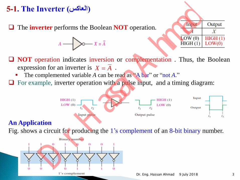
The inverter performs the Boolean NOT operation.
NOT operation indicates inversion or complementation . Thus, the Boolean
expression for an inverter is . The complemented variable A can be read as “A bar” or “not A.”
For example, inverter operation with a pulse input, and a timing diagram:
An Application
Fig. shows a circuit for producing the 1’s complement of an 8-bit binary number.
9 July 2018 Dr. Eng. Hassan Ahmad 3
X A
Dr. H
assan A
hmad

A waveform is applied to an inverter in Figure. Determine the
output waveform corresponding to the input and show the timing diagram.
According to the placement of the bubble, what is the active output state?
The output waveform is exactly opposite to the input (inverted), as shown in Fig.,
which is the basic timing diagram.
9 July 2018 Dr. Eng. Hassan Ahmad 4
Dr. H
assan A
hmad

The AND gate produces a HIGH output when all inputs are HIGH; otherwise,
the output is LOW.
The distinctive shape ( المميز الشكل ) symbol
For a 2-input gate, the truth table is
AND Gate Truth Table
The total number of possible combinations
of binary inputs to a AND gate is determined
by the following formula: , where N is the number of possible input
combinations and n is the number of input variables.
For example,
9 July 2018 Dr. Eng. Hassan Ahmad 5
2nN
Dr. H
assan A
hmad
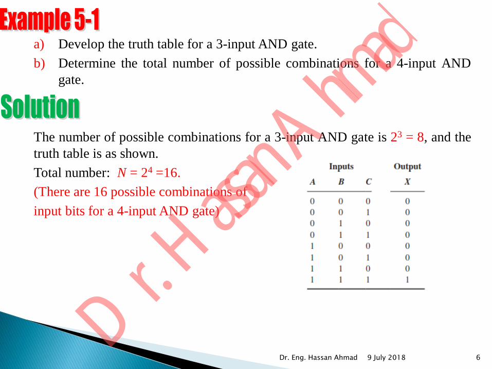
a) Develop the truth table for a 3-input AND gate.
b) Determine the total number of possible combinations for a 4-input AND
gate.
The number of possible combinations for a 3-input AND gate is 23 = 8, and the
truth table is as shown.
Total number: N = 24 =16.
(There are 16 possible combinations of
input bits for a 4-input AND gate)
9 July 2018 Dr. Eng. Hassan Ahmad 6
Dr. H
assan A
hmad
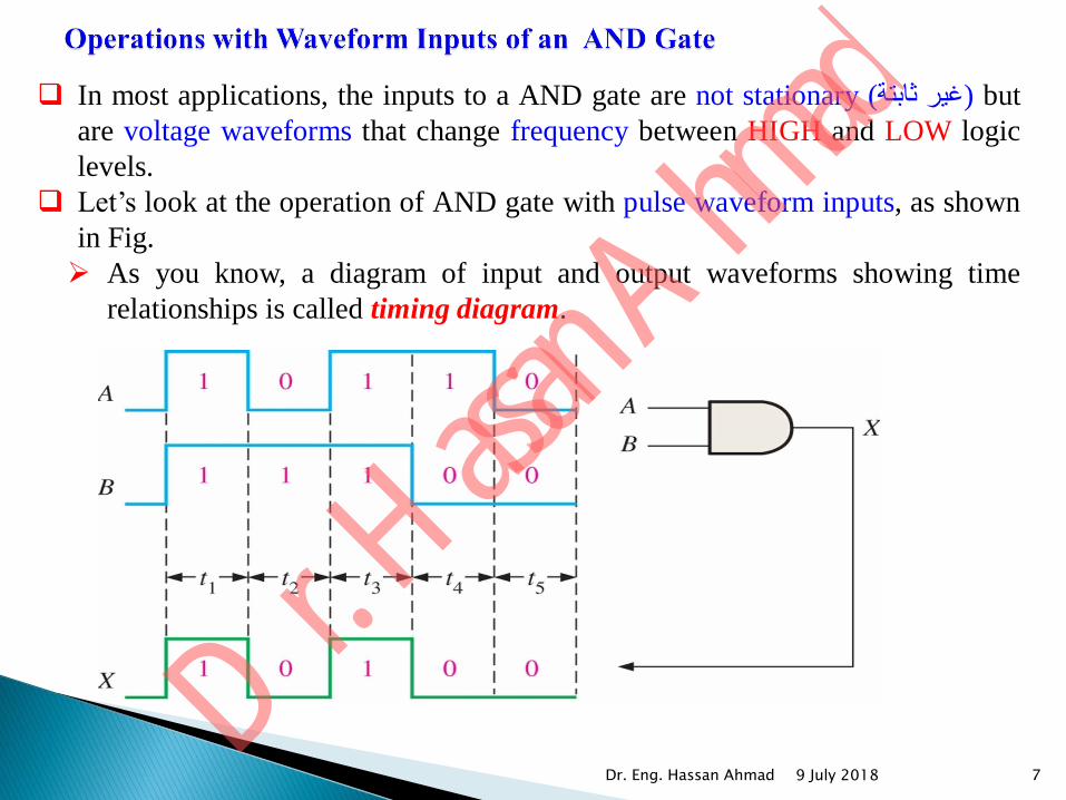
In most applications, the inputs to a AND gate are not stationary ( ثابتة غير ) but
are voltage waveforms that change frequency between HIGH and LOW logic
levels.
Let’s look at the operation of AND gate with pulse waveform inputs, as shown
in Fig.
As you know, a diagram of input and output waveforms showing time
relationships is called timing diagram.
9 July 2018 Dr. Eng. Hassan Ahmad 7
Dr. H
assan A
hmad
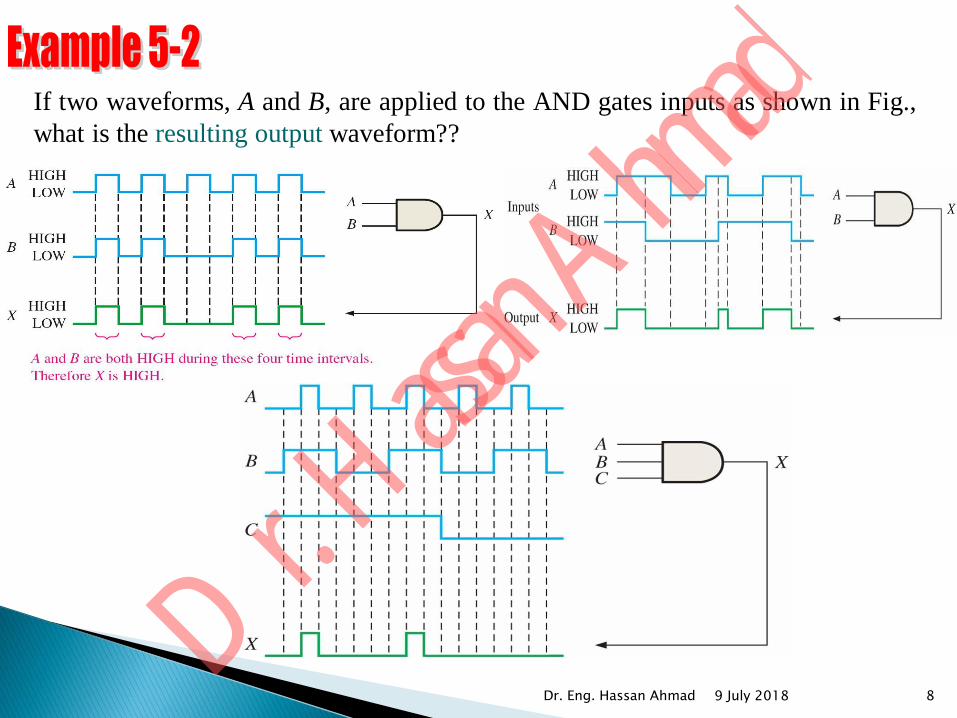
If two waveforms, A and B, are applied to the AND gates inputs as shown in Fig.,
what is the resulting output waveform??
9 July 2018 Dr. Eng. Hassan Ahmad 8
Dr. H
assan A
hmad

The logical AND function of two variables is represented mathematically as:
Boolean Multiplication ( البوليني الضرب )
Figure shows the AND gate logic symbol with two, three, and four inputs.
9 July 2018 Dr. Eng. Hassan Ahmad 9
orX A B X AB
Dr. H
assan A
hmad

The OR gate produces a HIGH output if any input is HIGH; if all inputs
are LOW, the output is LOW.
The distinctive shape ( المميز الشكل ) symbol
For a 2-input gate, the truth table is
The OR operation is shown with a plus sign (+) between the variables.
Thus, the OR operation is written as
9 July 2018 Dr. Eng. Hassan Ahmad 10
X A B
Dr. H
assan A
hmad

Example of OR gate operation with a timing diagram showing input and output
time relationships.
9 July 2018 Dr. Eng. Hassan Ahmad 11
Dr. H
assan A
hmad

If two input waveforms, A and B, are applied to the OR gate as
shown in Fig., what is the resulting output waveform??
9 July 2018 Dr. Eng. Hassan Ahmad 12
For the two and three input waveforms, A and B, in Fig., show the resulting output
waveform with its proper relation to the inputs?
Dr. H
assan A
hmad

The logic AND function of two variables is represented mathematically as
Boolean Addition
Notice that Boolean addition differs from binary addition in the case where
two 1s are added. There is no carry in Boolean addition.
Boolean expression for OR gates with two, three, and four inputs.
9 July 2018 Dr. Eng. Hassan Ahmad 13
X A B
Dr. H
assan A
hmad

The term NAND is contraction (اختصار) of NOT-AND and implies an AND
function with inverted output.
The NAND gate produces a LOW output when all inputs are HIGH;
otherwise, the output is HIGH. For a 2-input gate, the truth table is
The Boolean expression for the output of a 2-input NAND gate is shown
with a dot between the variables and an bar over covering them. Thus, the
NAND operation is written as
and all possible values of the two input variables
Are shown in Table.
9 July 2018 Dr. Eng. Hassan Ahmad 14
orX A B X AB
Dr. H
assan A
hmad

If two waveforms, A and B, are applied to the NAND gate
inputs as shown in Fig., determine the resulting output
waveform??
9 July 2018 Dr. Eng. Hassan Ahmad 15
Show the resulting output waveform for 3-inputs NAND gate with its proper
relation to the inputs?
Dr. H
assan A
hmad

The term NOR is contraction of NOT-OR and implies an OR function with
inverted output.
The NOR gate produces a LOW output if any input is HIGH; if all inputs are
HIGH, the output is LOW. For a 2-input gate, the truth table is
The Boolean expression for the output of a 2-input NOR gate can be written as
shown with a plus sign (+) between the variables and an over-bar covering them.
Thus, the NOR operation is written as
9 July 2018 Dr. Eng. Hassan Ahmad 16
X A B
Dr. H
assan A
hmad

If two (three) waveforms, A and B, (and C) are applied to the
NOR gate inputs as in shown Fig., determine the resulting
output waveform??
9 July 2018 Dr. Eng. Hassan Ahmad 17
Dr. H
assan A
hmad

The Exclusive-OR (XOR for short) produces a HIGH output only when
both inputs are at opposite logic levels. The truth table is
The XOR operation is written logically as
Example waveforms:
Notice that the XOR gate will produce a HIGH only when exactly one
input is HIGH.
9 July 2018 Dr. Eng. Hassan Ahmad 18
X AB AB
Dr. H
assan A
hmad

The Exclusive-NOR gate (XNOR) produces a HIGH output only when
both inputs are at the same logic level. The truth table is
The XOR operation shown as
Example of exclusive-OR gate operation with pulse waveform inputs.
9 July 2018 Dr. Eng. Hassan Ahmad 19
X A B A B
Dr. H
assan A
hmad

Determine the output waveforms for the XOR gate and for the
XNOR gate, given the input waveforms, A and B, in Fig.
The output waveforms are shown in Fig.
Notice that the XOR output is HIGH only when both inputs are at opposite
levels.
Notice that the XNOR output is HIGH only when both inputs are the same.
9 July 2018 Dr. Eng. Hassan Ahmad 20
Dr. H
assan A
hmad
9 July 2018 Dr. Eng. Hassan Ahmad 21
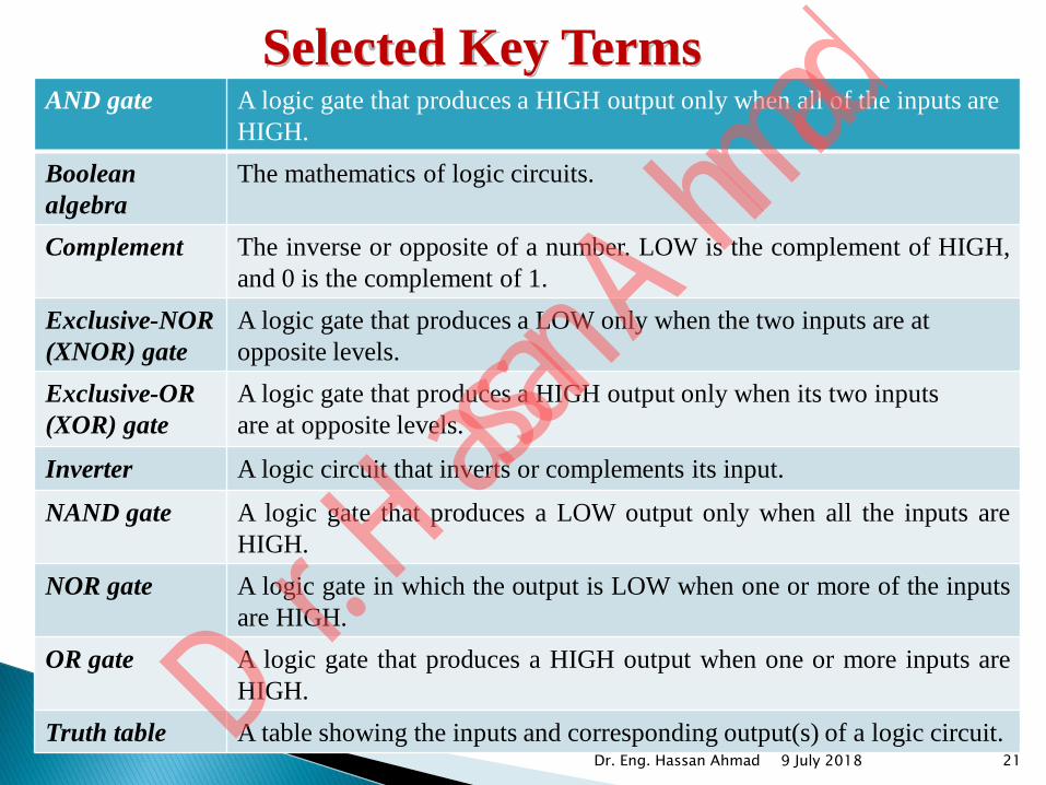
Selected Key Terms AND gate A logic gate that produces a HIGH output only when all of the inputs are
HIGH.
Boolean
algebra
The mathematics of logic circuits.
Complement The inverse or opposite of a number. LOW is the complement of HIGH,
and 0 is the complement of 1.
Exclusive-NOR
(XNOR) gate
A logic gate that produces a LOW only when the two inputs are at
opposite levels.
Exclusive-OR
(XOR) gate
A logic gate that produces a HIGH output only when its two inputs
are at opposite levels.
Inverter A logic circuit that inverts or complements its input.
NAND gate A logic gate that produces a LOW output only when all the inputs are
HIGH.
NOR gate A logic gate in which the output is LOW when one or more of the inputs
are HIGH.
OR gate A logic gate that produces a HIGH output when one or more inputs are
HIGH.
Truth table A table showing the inputs and corresponding output(s) of a logic circuit. Dr. H
assan A
hmad
9 July 2018 Dr. Eng. Hassan Ahmad 22
Dr. H
assan A
hmad

9 July 2018 Dr. Eng. Hassan Ahmad 23
Dr. H
assan A
hmad

9 July 2018 Dr. Eng. Hassan Ahmad 24
Dr. H
assan A
hmad

The input waveform shown in Fig. is applied to an inverter. Draw the
output waveform in proper relation to the input.
9 July 2018 Dr. Eng. Hassan Ahmad 25
Dr. H
assan A
hmad

If the waveform in Fig. is applied to point A of combination of
inverters shown in Fig., determine the waveforms at points B through F.
9 July 2018 Dr. Eng. Hassan Ahmad 26
Dr. H
assan A
hmad

Determine the output, X, for a 2-input AND gate with the input
waveforms shown in Fig. Show the proper relationship of output to inputs with
a timing diagram.
9 July 2018 Dr. Eng. Hassan Ahmad 27
Dr. H
assan A
hmad

The input waveforms applied to a 3-input AND gate are as indicated
in Fig. Show the output waveform in proper relation to the inputs with a timing
diagram.
9 July 2018 Dr. Eng. Hassan Ahmad 28
Dr. H
assan A
hmad
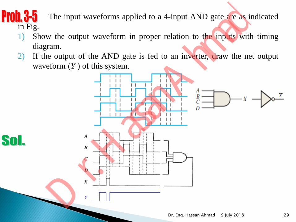
The input waveforms applied to a 4-input AND gate are as indicated
in Fig.
1) Show the output waveform in proper relation to the inputs with timing
diagram.
2) If the output of the AND gate is fed to an inverter, draw the net output
waveform (Y ) of this system.
9 July 2018 Dr. Eng. Hassan Ahmad 29
Dr. H
assan A
hmad

Determine the output for a 2-input OR gate when the input
waveforms are as shown in Fig. and draw a timing diagram.
9 July 2018 Dr. Eng. Hassan Ahmad 30
Dr. H
assan A
hmad

For the five input waveforms in Fig., determine the output for a 5-
input AND gate and the output for a 5-input OR gate. Draw the timing
diagram.
9 July 2018 Dr. Eng. Hassan Ahmad 31
Dr. H
assan A
hmad

For the set of input waveforms in Fig., determine the output for the
NAND Gate shown and draw the timing diagram.
9 July 2018 Dr. Eng. Hassan Ahmad 32
Dr. H
assan A
hmad

Determine the gate output for the input waveforms in Fig. and draw
the timing diagram.
9 July 2018 Dr. Eng. Hassan Ahmad 33
Dr. H
assan A
hmad
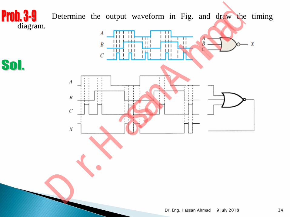
Determine the output waveform in Fig. and draw the timing
diagram.
9 July 2018 Dr. Eng. Hassan Ahmad 34
Dr. H
assan A
hmad
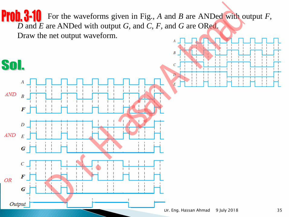
For the waveforms given in Fig., A and B are ANDed with output F,
D and E are ANDed with output G, and C, F, and G are ORed.
Draw the net output waveform.
9 July 2018 Dr. Eng. Hassan Ahmad 35
Dr. H
assan A
hmad

Determine the output waveform in Fig.
9 July 2018 Dr. Eng. Hassan Ahmad 36
Dr. H
assan A
hmad

9 July 2018
Dr. Eng. Hassan Ahmad 37
Dr. H
assan A
hmad