LNO-6xM-RF Operating Manual
52
Frequency Synthesizer LNO-6xM Operating Manual Rev. 1.2 Advantex LLC March 4, 2016 Russian Federation, 111250, Moscow, Krasnokazarmennaya st., 13/1 tel. +7 (495) 721-47-74, +7(495) 728-08-03 [email protected] http://advantex-rf.com, www.advantex.ru dvanteX IF/RF & Microwave Design
Transcript of LNO-6xM-RF Operating Manual

Frequency SynthesizerLNO-6xM
Operating ManualRev. 1.2
Advantex LLC
March 4, 2016
Russian Federation, 111250, Moscow,Krasnokazarmennaya st., 13/1tel. +7 (495) 721-47-74, +7(495) [email protected]://advantex-rf.com, www.advantex.ru
dvanteXIF/RF & Microwave Design


dvanteX LNO-6xM-RFFrequency Synthesizer 0.1-12GHz
IF/RF & Microwave Design
CONTENTS www.advantex-rf.com
Document RevisionsRev. Date Description1.0 February
3, 2015LNO Frequency Synthesizer Manual (starting fromLNO-62M-RF)
1.1 March 31,2015
Revised section 5.3
1.2 March 04,2016
Revised table 1 (power consumption)
Contents1 Getting Started 7
1.1 Interfaces and Connectors . . . . . . . . . . . . . . . . . . . . . . 71.2 LNO-6xM-KIT and LNO-SS6xM-KIT Evaluation Boards . . . . 91.3 RFCTL Evaluation Board . . . . . . . . . . . . . . . . . . . . . . 14
2 Remote Control 162.1 Quick Start . . . . . . . . . . . . . . . . . . . . . . . . . . . . . . 172.2 SCPI Commands . . . . . . . . . . . . . . . . . . . . . . . . . . . 17
2.2.1 SCPI Compliance . . . . . . . . . . . . . . . . . . . . . . . 172.2.2 SCPI Summary . . . . . . . . . . . . . . . . . . . . . . . . 19
2.3 SCPI Command List . . . . . . . . . . . . . . . . . . . . . . . . . 202.3.1 *CLS . . . . . . . . . . . . . . . . . . . . . . . . . . . . . 202.3.2 *IDN? . . . . . . . . . . . . . . . . . . . . . . . . . . . . . 202.3.3 *RST . . . . . . . . . . . . . . . . . . . . . . . . . . . . . 212.3.4 *OPC? . . . . . . . . . . . . . . . . . . . . . . . . . . . . 212.3.5 SYSTem:ERRor[:NEXT]? . . . . . . . . . . . . . . . . . . 212.3.6 OUTPut[:STATe] . . . . . . . . . . . . . . . . . . . . . . . 212.3.7 OUTPut:ROSCillator[:STATe] . . . . . . . . . . . . . . . 222.3.8 [SOURce:]FREQuency[:CW] . . . . . . . . . . . . . . . . 222.3.9 [SOURce:]POWer[:LEVel][:IMMediate][:AMPLitude] . . . 222.3.10 [SOURce:]PHASe[:ADJust] . . . . . . . . . . . . . . . . . 232.3.11 [SOURce:]ROSCillator:SOURce . . . . . . . . . . . . . . . 232.3.12 [SOURce:]ROSCillator:EXTernal:FREQuency . . . . . . . 232.3.13 MEASure[:SCALar]:TEMPerature? . . . . . . . . . . . . . 242.3.14 STATus:QUEStionable:CONDition? . . . . . . . . . . . . 242.3.15 STATus:QUEStionable[:EVENt]? . . . . . . . . . . . . . . 24
3 Evaluation Board Firmware Update 25
4 LNO-6xM SPI Registers and Commands 284.1 General Description . . . . . . . . . . . . . . . . . . . . . . . . . 284.2 Format of SPI Commands . . . . . . . . . . . . . . . . . . . . . . 304.3 SPI Commands . . . . . . . . . . . . . . . . . . . . . . . . . . . . 31
4.3.1 Func register writing C[7:0]=0x01 . . . . . . . . . . . . . 31
3
dvanteX LNO-6xM-RFFrequency Synthesizer 0.1-12GHz
IF/RF & Microwave Design
www.advantex-rf.com LIST OF FIGURES
4.3.2 Func register reading C[7:0]=0x81 . . . . . . . . . . . . . 314.3.3 Divider buffer register writing C[7:0]=0x02 . . . . . . . . 314.3.4 Divider buffer register reading C[7:0]=0x82 . . . . . . . . 314.3.5 Gain buffer register writing C[7:0]=0x03 . . . . . . . . . . 314.3.6 Gain buffer register reading C[7:0]=0x83 . . . . . . . . . . 344.3.7 DigPotWP register writing C[7:0]=0x04 . . . . . . . . . . 344.3.8 DigPotWP register reading C[7:0]=0x84 . . . . . . . . . . 344.3.9 MuxOut register writing C[7:0]=0x05 . . . . . . . . . . . 344.3.10 MuxOut register reading C[7:0]=0x85 . . . . . . . . . . . 364.3.11 DDS_SPI Access C[7:0]=0x10 . . . . . . . . . . . . . . . 364.3.12 Toggling DDS_IOUPDATE C[7:0]=0x11 . . . . . . . . . 364.3.13 Divider register updating C[7:0]=1x12 . . . . . . . . . . . 364.3.14 Gain register updating C[7:0]=1x13 . . . . . . . . . . . . 364.3.15 All register updating and DDS_IOUPDATE toggling C[7:0]=1x1F 364.3.16 TEMP_SPI Access C[7:0]=0x30 . . . . . . . . . . . . . . 374.3.17 ADC_SPI Access C[7:0]=0x40 . . . . . . . . . . . . . . . 374.3.18 DIGPOT_SPI Access C[7:0]=0x50 . . . . . . . . . . . . . 374.3.19 FLASH_SPI Access C[7:0]=0x70 . . . . . . . . . . . . . . 37
5 LNO-6xM SPI Programming 375.1 Parameter Calculations . . . . . . . . . . . . . . . . . . . . . . . 375.2 Initialization . . . . . . . . . . . . . . . . . . . . . . . . . . . . . 405.3 Setting Frequency, Phase and Level . . . . . . . . . . . . . . . . . 415.4 Reading internal temperature . . . . . . . . . . . . . . . . . . . . 425.5 Flash Memory . . . . . . . . . . . . . . . . . . . . . . . . . . . . 43
5.5.1 FLASH_CMD_READ (0x03) . . . . . . . . . . . . . . . 435.5.2 FLASH_CMD_WRITE (0x02) . . . . . . . . . . . . . . . 445.5.3 FLASH_CMD_WREN (0x06) . . . . . . . . . . . . . . . 445.5.4 FLASH_CMD_WRDI (0x04) . . . . . . . . . . . . . . . 455.5.5 FLASH_CMD_RDSR (0x05) . . . . . . . . . . . . . . . . 455.5.6 FLASH_CMD_WRSR (0x01) . . . . . . . . . . . . . . . 465.5.7 FLASH_CMD_PE (0x42) . . . . . . . . . . . . . . . . . 465.5.8 FLASH_CMD_SE (0xD8) . . . . . . . . . . . . . . . . . 465.5.9 FLASH_CMD_CE (0xC7) . . . . . . . . . . . . . . . . . 465.5.10 FLASH_CMD_RDID (0xAB) . . . . . . . . . . . . . . . 465.5.11 FLASH_CMD_PDP (0xB9) . . . . . . . . . . . . . . . . 47
5.6 Memory address and data mapping . . . . . . . . . . . . . . . . . 475.6.1 Configuration Block . . . . . . . . . . . . . . . . . . . . . 505.6.2 Data block . . . . . . . . . . . . . . . . . . . . . . . . . . 51
List of Figures
1 RF Out Connector . . . . . . . . . . . . . . . . . . . . . . . . . . 72 REF In and SPI Connectors . . . . . . . . . . . . . . . . . . . . . 73 SPI Control and Power Supply interface . . . . . . . . . . . . . . 8
4

dvanteX LNO-6xM-RFFrequency Synthesizer 0.1-12GHz
IF/RF & Microwave Design
LIST OF TABLES www.advantex-rf.com
4 RS2SPI Evaluation Board . . . . . . . . . . . . . . . . . . . . . . 105 COM-port number . . . . . . . . . . . . . . . . . . . . . . . . . . 116 Select SPI-connector number . . . . . . . . . . . . . . . . . . . . 117 COM-port configuration . . . . . . . . . . . . . . . . . . . . . . . 128 LNO tab . . . . . . . . . . . . . . . . . . . . . . . . . . . . . . . . 139 LNO reference frequency source control . . . . . . . . . . . . . . 1410 Drain current setting of output amplifier . . . . . . . . . . . . . . 1511 RFCTL Evaluation Board . . . . . . . . . . . . . . . . . . . . . . 1612 Example of the remote control using HyperTerminal application 1813 COM-port settings . . . . . . . . . . . . . . . . . . . . . . . . . . 1814 Instrument control and command processing model . . . . . . . . 1915 Command structure . . . . . . . . . . . . . . . . . . . . . . . . . 2016 Device Manager window (My Computer .Manage) . . . . . . . . . 2617 Firmware update application – XMI Programmer . . . . . . . . . 2718 LNO synthesizer block diagram . . . . . . . . . . . . . . . . . . . 2919 LNO SPI writing cycle diagram . . . . . . . . . . . . . . . . . . . 3020 Command and data bytes . . . . . . . . . . . . . . . . . . . . . . 3021 LNO SPI reading cycle diagram . . . . . . . . . . . . . . . . . . . 3022 Writing 1 data byte . . . . . . . . . . . . . . . . . . . . . . . . . 3123 Input and output data for LNO programming . . . . . . . . . . . 3824 Bilinear interpolation . . . . . . . . . . . . . . . . . . . . . . . . . 4025 Structure of flash-memory data transfer . . . . . . . . . . . . . . 4326 Flash-memory data read command . . . . . . . . . . . . . . . . . 4327 Flash-memory data write command . . . . . . . . . . . . . . . . . 4428 Flash-memory write enable command . . . . . . . . . . . . . . . 4429 Flash-memory write/erase disable command . . . . . . . . . . . . 4530 Flash-memory status register reading . . . . . . . . . . . . . . . . 4531 Flash-memory write to status register . . . . . . . . . . . . . . . 4632 Flash-memory page erase command . . . . . . . . . . . . . . . . . 4633 Flash-memory byte erase command . . . . . . . . . . . . . . . . . 4734 Flash-memory clear all command . . . . . . . . . . . . . . . . . . 4735 Flash-memory power on and read ID command . . . . . . . . . . 4736 Flash-memory power off command . . . . . . . . . . . . . . . . . 51
List of Tables1 SPI Control and Power Supply pinout . . . . . . . . . . . . . . . 82 LNO SPI Commands C[7:0] . . . . . . . . . . . . . . . . . . . . . 323 Func register . . . . . . . . . . . . . . . . . . . . . . . . . . . . . 334 Divider register . . . . . . . . . . . . . . . . . . . . . . . . . . . . 335 Gain register . . . . . . . . . . . . . . . . . . . . . . . . . . . . . 346 DigPotWP register . . . . . . . . . . . . . . . . . . . . . . . . . . 347 MuxOut register . . . . . . . . . . . . . . . . . . . . . . . . . . . 358 LNO input parameters . . . . . . . . . . . . . . . . . . . . . . . . 399 Intermediate variables and output parameters . . . . . . . . . . . 39
5
dvanteX LNO-6xM-RFFrequency Synthesizer 0.1-12GHz
IF/RF & Microwave Design
www.advantex-rf.com LIST OF TABLES
10 Turning on the internal power supply system at initialization pro-cess . . . . . . . . . . . . . . . . . . . . . . . . . . . . . . . . . . 41
11 Turning on the DDS power supply at initialization process . . . . 4112 Flash-memory commands . . . . . . . . . . . . . . . . . . . . . . 4313 Flash-memory status register . . . . . . . . . . . . . . . . . . . . 4514 Flash-memory block protection . . . . . . . . . . . . . . . . . . . 4615 Memory address and data mapping . . . . . . . . . . . . . . . . . 4716 Type of Data Table (CTYPE) . . . . . . . . . . . . . . . . . . . . 5117 X,Y and Z-data format (XVALUE, YVALUE, ZVALUE) . . . . . 52
6
dvanteX LNO-6xM-RFFrequency Synthesizer 0.1-12GHz
IF/RF & Microwave Design
1 GETTING STARTED www.advantex-rf.com
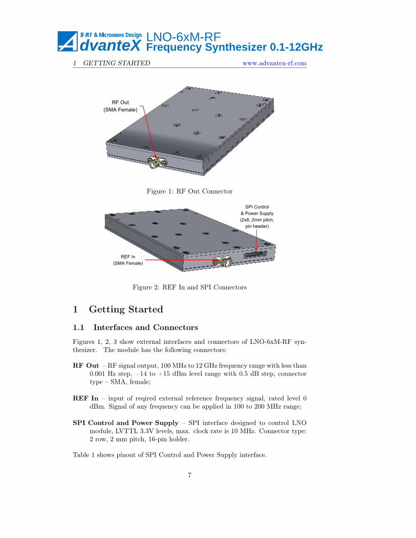
RF Out(SMA Female)
Figure 1: RF Out Connector
REF In(SMA Female)
SPI Control & Power Supply(2x8, 2mm pitch,
pin header)
Figure 2: REF In and SPI Connectors
1 Getting Started
1.1 Interfaces and Connectors
Figures 1, 2, 3 show external interfaces and connectors of LNO-6xM-RF syn-thesizer. The module has the following connectors:
RF Out – RF signal output, 100 MHz to 12 GHz frequency range with less than0.001 Hz step, −14 to +15 dBm level range with 0.5 dB step, connectortype – SMA, female;
REF In – input of reqired external reference frequency signal, rated level 0dBm. Signal of any frequency can be applied in 100 to 200 MHz range;
SPI Control and Power Supply – SPI interface designed to control LNOmodule, LVTTL 3.3V levels, max. clock rate is 10 MHz. Connector type:2 row, 2 mm pitch, 16-pin holder.
Table 1 shows pinout of SPI Control and Power Supply interface.
7

dvanteX LNO-6xM-RFFrequency Synthesizer 0.1-12GHz
IF/RF & Microwave Design
www.advantex-rf.com 1 GETTING STARTED
Pin 1
Pin 2Pin 16
Pin 15
Figure 3: SPI Control and Power Supply interface
Table 1: SPI Control and Power Supply pinoutPin # Name Direction
(relativeto
module)
Description
1 LNO_MOSI In SPI master output, slave input3 LNO_SS# In SPI select signal, data are latched only if this
signal is active (“0” state)5 LNO_SCK In SPI clock signal, data are latched by rising
edge of LNO_SCK signal7 LNO_MISO Out SPI master input, slave output8 LNO_AUX Out LNO_AUX signal can be programmed as PLL
lock status output, fixed low or high stateoutput, and as the output of internal updatesignal of the loaded data (see section 4.3.9 formore details). This pin is connected to CPLDvia 1 kOhm resistor, so if not used you can tieit to the GND
2, 10,12,
14, 16
GND – Ground pins, internally connected to the casebody
4, 6 – – AC ground. Internally connected via 1 uFcapacitors to GND
9, 11 +5V In Positive power supply, +5.0 to +5.5V allowed.Rated current 0.18A
13, 15 +9V In Positive power supply, +9 to +12V allowed,but to reduce overheating and powerconsumption it’s better not to exceed +10V.Rated current 0.78A
8

dvanteX LNO-6xM-RFFrequency Synthesizer 0.1-12GHz
IF/RF & Microwave Design
1 GETTING STARTED www.advantex-rf.com
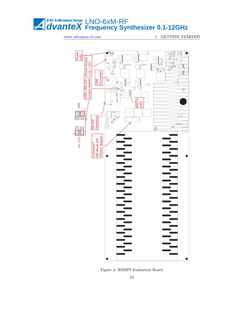
1.2 LNO-6xM-KIT and LNO-SS6xM-KIT Evaluation Boards
LNO-6xM-KIT includes LNO Frequency Synthesizer and RS2SPI evaluationboard (fig. 4). LNO-SS6xM-KIT also includes DSG-3xM-RF frequency syn-thesizer as the reference frequency source which is used for additional spursuppression and enchanced synchronization capability (see section 1.3). It isdesigned for quick start and helps to understand SPI protocol command set andalgorithms used to control LNO synthesizer. All SPI commands which sent tothe module are displayed in log window of the application. So you can easilycheck yourself while debugging of your own control system of the synthesizer.For remote control of LNO (LNO+DSG) module follow the steps below.
1. Connect LNO module to the RS2SPI board (Connector 1 located on thetop side of the board, see fig. 4) via SPI cable (16-pin, 2-mm pitch, IDCflat cable).
2. Connect DSG module to the RS2SPI board (Connector 2 located on thebottom side of the board) via SPI cable (16-pin, 2-mm pitch, IDC flatcable).
3. Connect RS2SPI board to PC via USB or RS-232 cable (see jumper posi-tions for USB/RS-232 use on fig. 4)
4. Connect RS2SPI board to +12VDC power supply. Max current of thepower supply source should be set to 3A for the DC-DC converters ofRS2SPI board to start. Turn on the power. Power supply consumptionwill be about 0.1A (for non-initialized LNO and DSG modules).
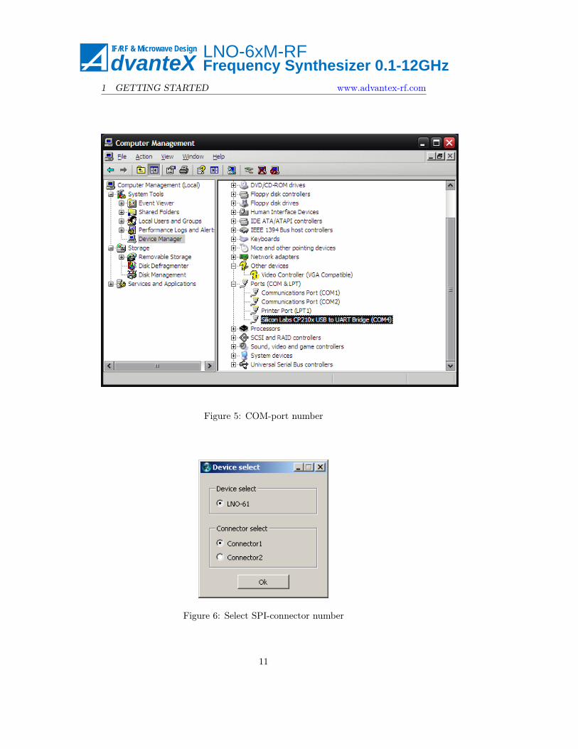
5. When using USB cable find out the COM-port number in Computer Man-agement window (see fig. 5) You can specify another COM-port number(Properties .Port Settings .Advanced .COM Port Number).
6. Launch RF Debug Application (double click on advantex.exe or advantex.tclif you have Tcl/Tk installed).
7. Select radio-boxes as shown on the fig. 6 (specify the connector of theRS2SPI board to which LNO is connected) and click OK.
8. Select menu Setup .COM_configure and specify COM-port number (fig.7) as it was determined in fig. 5. Click OK.
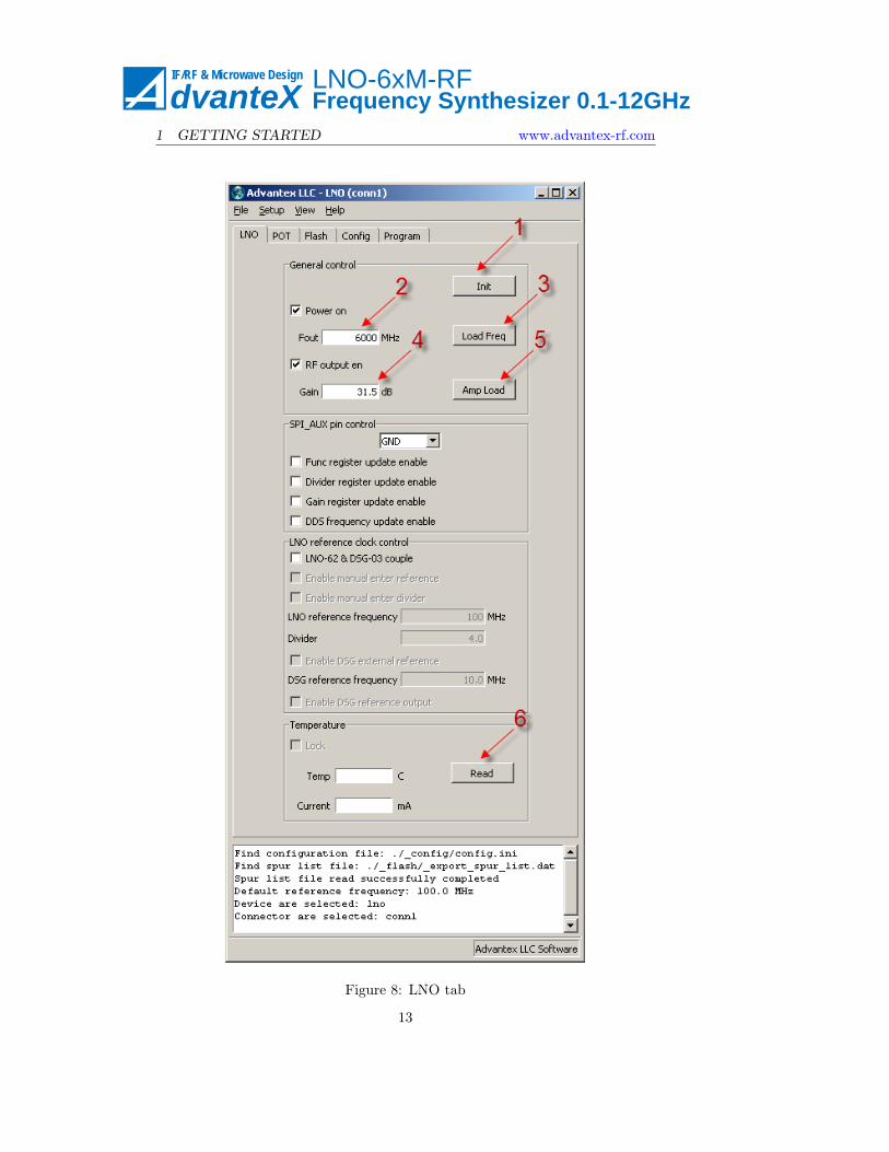
9. To start working with LNO-module press Init button (fig. 8, Item 1),then you can load frequency or output level without Init button. To loadfrequency you need to set value in MHz (Item 2) and press Load button(Item 3). Output level adjustment is implemented by loading a gain value(Item 4) which is in range 0 to 31.5 dB with 0.5 dB step. It correspondsto the digital attenuator setting, where 0 - maximum attenuation, 31.5- minimum attenuation. You can read the internal temperature of theblock and the output stage drain current by pressing Read button (Item
9
dvanteX LNO-6xM-RFFrequency Synthesizer 0.1-12GHz
IF/RF & Microwave Design
www.advantex-rf.com 1 GETTING STARTED
2 2
1 1
56
2 16
+ -
1
1 1
1
2
1
1
2
1
2
+
10 9
-
2 1
12
1 15
R26 VT5R25
VT2 C28
C26
C22
C20 VD5
C1
C2 C10
R36
R7
C58
DD4
XP13
XP14XP15 VD6 C56
XP2
XP11
R41 C43
R21
C8L5
C39
R17 C40
R24 R32VD7 R
28
R29
C13 VT4
R34
R42 R9XP12
C24C27 C35 C
12
R14 C23DA2
R39
XP5
C25 DA1 VT3
C36
R16
R8
DA5
C17R13
C11
R1
R15 L4R40
C47
R2 R4 R3 C18 R5
DA4
VT1
DA3
VD4 C37DD3
R38
VD2
VD1
C34
R6 C31
VD3
L7R10
R11C19
R37 C48
XP7XP6
L2
L1
C55
ZC4L3
XS1
C57
C33 C32
XP10C30 C29
C4
C7
C5
C6 XP8 XP9
C9
DD1
C14
R27
DD2
C42 C16
C15
ZQ1
ZC3ZC1
C41
XP1 ZC2
XP3
R23DA6
R12
R18 R22
C3
R20 XW1
C50C52
C51
R19 C45C54C44
C46
C53RS-232
Connector
USB
Connector
USB/RS-232
JumperSwitch
PowerSupply
+12..+15V
RX/TX
LED
USB
RS-232
11
Power
LED
Connector1
(RF-BlockSPI
+PowerSupply)
Figure 4: RS2SPI Evaluation Board
10
dvanteX LNO-6xM-RFFrequency Synthesizer 0.1-12GHz
IF/RF & Microwave Design
1 GETTING STARTED www.advantex-rf.com
Figure 5: COM-port number
Figure 6: Select SPI-connector number
11

dvanteX LNO-6xM-RFFrequency Synthesizer 0.1-12GHz
IF/RF & Microwave Design
www.advantex-rf.com 1 GETTING STARTED
Figure 7: COM-port configuration
6). For LNO+DSG configuration (LNO-SS6xM-KIT) set the LNO-62 &DSG-03 couple checkbox and press Init button. After pressing Init buttonpower consumption will increase up to 0.8A for LNO-6xM-KIT, and 1.2Afor LNO-SS6xM-KIT (LNO+DSG configuration).
10. In LNO+DSG configuration the DSG synthesizer is used as the refer-ence frequency source for the high frequency LNO synthesizer. Choosingthe right LNO reference frequency value defines the quality of LNO RFOut signal (in terms of spurs). You can set this frequency manually bysetting the Enable manual reference checkbox or automatically (the check-box is unset). In this case new reference frequency is calculated eachtime you press Load Freq button using the frequency table located in_export_spur_list.dat data file. If you need to use DSG external ref-erence, please check the box Enable DSG external reference (fig. 9), set theDSG reference frequency value in range 1 to 250 MHz and press Init button(fig. 8, Item 1). Each change of any checkbox setting requires the pressingof Init button to load new settings to the hardware.
11. The POT tab described below (fig. 10) is used only in the factory ad-justment of the drain current of output amplifier. After adjustment thesetting is stored in FLASH memory of digital potentiometer and is appliedautomatically after power on of the LNO module. To adjust drain currentfollow these steps.
! Dig POT tab settings are not
used in normal operation.
(a) Load the Digital Potentiometer DAC value (in range 0 to 1023) usingDig POT field (Item 1) and Write(DAC) button (Item 2). 0 corre-sponds to the maximum current, 1023 corresponds to the minimum
12
dvanteX LNO-6xM-RFFrequency Synthesizer 0.1-12GHz
IF/RF & Microwave Design
1 GETTING STARTED www.advantex-rf.com
Figure 8: LNO tab
13

dvanteX LNO-6xM-RFFrequency Synthesizer 0.1-12GHz
IF/RF & Microwave Design
www.advantex-rf.com 1 GETTING STARTED
Figure 9: LNO reference frequency source control
current. For not to exceed maximum current ratings, please startwith 1023.
(b) Read the drain current value by pressing Read(curr) button (Item4).
(c) Repeat these steps until the current is set about 75 mA.
(d) Write the final value to the digital potentiometer FLASH by pressingStore(FLASH) button.
1.3 RFCTL Evaluation Board
RFCTL-1xM-PCB evaluation board can be used in two ways: (a) as the RS2SPIreplacement or (b) as the RF-module control PCB. In this case RF-modules(LNO and DSG) are controlled using SCPI command set via USB, RS-232 orUART interfaces. All calculations are performed by MCU of RFCTL board.Particular implementation depends on the firmware loaded to MCU located onthe RFCTL board.
For remote control of LNO (LNO+DSG) module follow the steps below.
1. Connect LNO module to the RFCTL board to SPI3 (Connector 1 in termsof RS2SPI, see fig. 11) via SPI cable (16-pin, 2-mm pitch, IDC flat cable).
2. Connect DSG module to the RFCTL board to SPI2 (Connector 2 in termsof RS2SPI) via SPI cable (16-pin, 2-mm pitch, IDC flat cable).
14

dvanteX LNO-6xM-RFFrequency Synthesizer 0.1-12GHz
IF/RF & Microwave Design
1 GETTING STARTED www.advantex-rf.com
Figure 10: Drain current setting of output amplifier
15

dvanteX LNO-6xM-RFFrequency Synthesizer 0.1-12GHz
IF/RF & Microwave Design
www.advantex-rf.com 2 REMOTE CONTROL
SPI1
SPI2
SPI3
IOBUS[7:0]
+12V GND
GPIO_0
GPIO_1
AUX In
USB14
PDI
LED
RS
-232
1 4
1 41
2
1 4
RFCTL-01M-PCB
Figure 11: RFCTL Evaluation Board
3. Connect RFCTL board to PC via USB (XP2 Connector: 1: VBUS, 2:D-, 3: D+, 4:GND ) or RS-232 cable (XP9 connector, 10-pin, 2.54-mmpitch, IDC flat cable). XP9 connector pinout is the following. Pins 1, 2and 7 (DCD, DSR, DTR) are internally connected and left floated. Pins4 and 6 (RTS, CTS) are internally connected and left floated. Pin 8 isnot connected. Pin 9 – GND. Pin 3 – TX (output), pin 5 – RX (input).This connector can be connected directly to the standard DB-9 femaleconnector via flat ribbon cable.
4. Connect RFCTL board to +12VDC power supply (X1 terminal block).
In variant (a) the remaining steps are identical to described in section 1.2. In(b) variant don’t launch RF Debug Application. You can use any applicationwhich can send chars to COM-port (e.g. standard Windows Hyper Terminalapplication) to control RF-modules with aid of standard SCPI commands.
2 Remote Control
In (b) variant the remote control of the RFCTL Evaluation Board is based onthe SCPI (Standard Commands for Programmable Instruments) protocol. It
16

dvanteX LNO-6xM-RFFrequency Synthesizer 0.1-12GHz
IF/RF & Microwave Design
2 REMOTE CONTROL www.advantex-rf.com
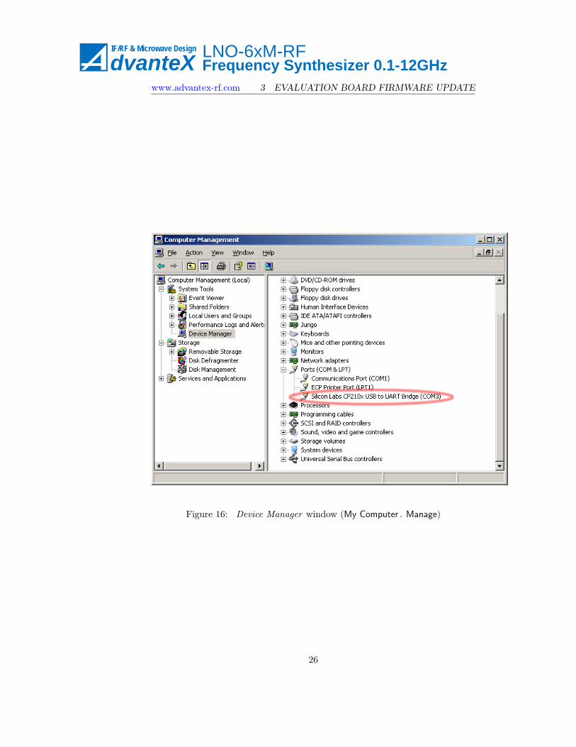
is implemented via RS-232 and USB interfaces located on the top side of theboard, fig. 11, (USB looks in OS like COM-port), so it can be easily managedby any software which has access to the COM-port of the PC. Only one portcan be active, the choice is automatic and remains the same until the power off.The choice of the active port occurs when any byte comes to the one of the ports(not necessary a valid command). The connection via USB is implemented withaid of USB to UART bridge, so from the view point of PC software it looks likea COM-port, fig. 16. This method requires driver installation 1 (integral circuitCP2102). The driver is available for the following OSes: Win2K/XP/2K3,Vista, Windows 7, Mac OS, Linux 3.1.
2.1 Quick StartAs a simple remote control application you can use the standard Windowsapplication – HyperTerminal (Start .Programs .Accessories .Communications .HyperTerminal) to send the SCPI commands to the instrument, fig. 12. COM-port settings are the following: 115200 bps, 8 data bits, parity none, 1 stopbit, flow control none, fig. 13. For more convenient use of the HyperTerminalit’s recommended to configure the settings (File .Properties, Settings tab, ASCIISetup. . . button) “Echo typed characters locally” and “Send line ends with linefeeds”. For example, the following typed sequence in HyperTerminal application
*rstfreq 100MHzpow -1dBm
will reset the instrument, set the output frequency to 100 MHz, and output RFlevel to −1 dBm.
2.2 SCPI CommandsFigure 14 shows the model of SCPI command processing.
2.2.1 SCPI Compliance
Instrument control command set is based on the SCPI v. 1999.0, but it’s notfully compatible. The differences are listed below:
• not all required commands are implemented (see the command list);
• command parser recognizes only one command in single string, and thestring size shall not exceed 64 symbols;
• command buffer length equals two, i.e. it is possible to send second com-mand after the first one immediately (not waiting for completion of thefirst command), but not more;
i In applications where one
command follows after another
immediately without any time delay,
for proper SCPI operation it is
recommended to use *OPC?
command
• status information is not fully supported;1The driver (its last version) can be downloaded from CP2102 bridge vendor site Silicon
Labs
17

dvanteX LNO-6xM-RFFrequency Synthesizer 0.1-12GHz
IF/RF & Microwave Design
www.advantex-rf.com 2 REMOTE CONTROL
Figure 12: Example of the remote control using HyperTerminal application
Figure 13: COM-port settings
18

dvanteX LNO-6xM-RFFrequency Synthesizer 0.1-12GHz
IF/RF & Microwave Design
2 REMOTE CONTROL www.advantex-rf.com
Input unit with input buffer
Command recognition
Data set /Instrument hardware
Status reporting system
Output unit with output buffer
RS-232USB
RS-232USB
Figure 14: Instrument control and command processing model
• not all data formats are supported;
• documentation doesn’t meet all the requirements of the standard.
2.2.2 SCPI Summary
Some notes listed below can help the newcomers to start the work with SCPIinstrument.
• SCPI-commands are not case sensitive, i.e. commands *RST and *rst areidentical.
• The first part of the command name, which is written in capitals, corre-sponds to a short form of the command. For example, to set frequencyyou can write FREQ, as well as FREQuency.
• Commands placed to the brackets are optional. For example the command[SOURce:]FREQuency[:CW] have the same effect when written in followingforms SOURce:FREQuency:CW,
• FREQuency:CW, SOURce:FREQuency, FREQuency.
• If command requires the numerical parameter expressed in some unitsthen the default unit exists. For example commands FREQ 1GHz, FREQ1E9Hz and FREQ 1000000000 sets the same frequency value 1 GHz, andthe default unit is one Hz.
19

dvanteX LNO-6xM-RFFrequency Synthesizer 0.1-12GHz
IF/RF & Microwave Design
www.advantex-rf.com 2 REMOTE CONTROL
OUTPut
STATe
SOURce
FREQuency POWer
CW LEVel
IMMediate
AMPLitude
PHASe
ADJust
GHZ, MHZ, MAHZ, KHZ,
HZDBM DEG, DEGree
ON, OFF, 0, 1
float number float number float number
Com
man
ds
Parameters or return values
Units
ROSCillator
EXTernal
FREQuency
SOURce
ROSCillator
STATe
MEASure
SCALar
TEMPerature
float number
GHZ, MHZ, MAHZ, KHZ,
HZ
INTernal, EXTernal
ON, OFF, 0, 1
(°C)
STATus
QUEStionable
integer
CONDition
Figure 15: Command structure
• Commands ending with a question mark, are the queries and return aresponse. For example the *IDN? command returns an instrument ID.Many commands that set some value, also have a query form to read thecurrent value, e.g. FREQ? – returns the current value of frequency.
• Commands that provide input of numerical parameters, can also take thefollowing: MINimum – minimum value, MAXimum – maximum value, DEFault– default value. For example FREQ MAX command sets the maximum fre-quency (8 GHz), and FREQ DEF sets 1 GHz (default value).
• If the entered command didn’t produce the desired effect, it’s worth check-ing the error buffer by means of request SYSTem:ERRor:[NEXT]?. If it werenot an error, the return value will be the following string 0,”No error”,otherwise it returns error code and short description.
2.3 SCPI Command ListFigure 15 represents the available command tree (except standard commands).Optional parts of commands are marked with dotted line.
2.3.1 *CLS
*CLS command clears error buffer.
2.3.2 *IDN?
This query command returns the string containing the information about the in-strument in the following format: manufacturer,part number,serial number,firmwareinfo.
20

dvanteX LNO-6xM-RFFrequency Synthesizer 0.1-12GHz
IF/RF & Microwave Design
2 REMOTE CONTROL www.advantex-rf.com
2.3.3 *RST
This command presets the instrument: frequency 1 GHz, level 0 dBm, phase 0degrees, RF output is off.
It’s a good practice to start the remote control process with the *RST com-mand.
2.3.4 *OPC?
This query command returns 1 after its completion. It means that all previouscommands are completed. It’s good practice to use this command instead offixed time delay between commands.
Examples: If you need to send several commands following immediately oneafter another, for example to set frequency and level, it’s recommended to do itthis way:
freq 100 mhz*opc?1pow 1 dbm*opc?1
2.3.5 SYSTem:ERRor[:NEXT]?
This query command returns the string containing the error code and its de-scription from the error buffer. If the buffer is empty then the returned stringcontains 0,”No error”.
Error buffer is organized in form of FIFO (First In First Out). If inputcommand doesn’t meet the requirements of parser, or for whatever reason cannot be executed, the corresponding message is placed to the error buffer. Thebuffer can contain 2 messages. There are two ways to clear the buffer: by readingthe errors with aid of SYST:ERR? command one by another, or using *CLScommand. When the buffer is already full, and one more error message comes,then the last error message will be rewritten by the following -350,"Queueoverflow".
2.3.6 OUTPut[:STATe]
The command turns on or off the RF output as the hardware RF OUT ON/OFFbutton located at the front panel do.
Parameters: To turn on the output: 1 or ON, to turn off – 0 or OFF.In query form the command returns 0 – if RF output is off, and 1 – if it’s
on.
21

dvanteX LNO-6xM-RFFrequency Synthesizer 0.1-12GHz
IF/RF & Microwave Design
www.advantex-rf.com 2 REMOTE CONTROL
Examples:
output onoutp offoutp:state 1OUTPUT 0OUTP:STAT?
2.3.7 OUTPut:ROSCillator[:STATe]
The command turns on and off the REF OUT output located on the rear panelof the instrument.
Parameters: To turn on the output: 1 or ON, to turn off – 0 or OFF.In query form the command returns 0 – if REF OUT output is off, and 1 –
if it’s on.
Examples:
output:rosc onoutp:rosc offoutp:rosc:state 1
2.3.8 [SOURce:]FREQuency[:CW]
The command sets output frequency
Parameters: Parameter has the following form[+|-]float_num[E[+|-]int_num][GHZ|MHZ|MAHZ|KHZ|HZ].The default unit is HZ. Input value is rounded with accuracy of 10−4. If the
specified value is out of valid range, then the nearest limit value is applied, errormessage will not be formed.
Query form of the command returns current frequency in Hz. The result hasthe following form: [+|-]float_num.
Examples:
freq 2.1GHZfrequency 21e-1ghzsour:freq:cw 21E8freq max
2.3.9 [SOURce:]POWer[:LEVel][:IMMediate][:AMPLitude]
The command sets RF output level.
22
dvanteX LNO-6xM-RFFrequency Synthesizer 0.1-12GHz
IF/RF & Microwave Design
2 REMOTE CONTROL www.advantex-rf.com
Parameters: Parameter has the following form[+|-]float_num[E[+|-]int_num][DBM].The default unit is DBM. Input value is rounded with accuracy of 10−2. If thespecified value is out of valid range, then the nearest limit value is applied, errormessage will not be formed.
Query form of the command returns current output level in dBm. The resulthas the following form: [+|-]float_num.
Examples:
pow 5.1dbmsource:power 1.23POWER 123E-2DBMPOW MAX
2.3.10 [SOURce:]PHASe[:ADJust]
The command sets RF signal phase offset.
Parameters: Parameter has the following form[+|-]float_num[E[+|-]int_num][DEGree].The default unit is DEGree. Input value is rounded with accuracy of 10−2. Ifthe specified value is out of valid range, then the nearest limit value is applied,error message will not be formed.
Query form of the command returns current phase offset in degrees. Theresult has the following form: [+|-]float_num.
Example:
phas 90degPHASE 90DEGphase:adj 90.1e-1
2.3.11 [SOURce:]ROSCillator:SOURce
The command turns on and off the REF IN input, i.e. switches between internaland external reference frequency source.
Parameters: Input parameter value may be INTernal – internal referencesource is used, or EXTernal – external reference source is used.
Query form of the command returns current source in use: INT or EXT.
Examples:
rosc:source INTrocs:sour ext
2.3.12 [SOURce:]ROSCillator:EXTernal:FREQuency
The command sets the value of external reference frequency at REF IN input.
23

dvanteX LNO-6xM-RFFrequency Synthesizer 0.1-12GHz
IF/RF & Microwave Design
www.advantex-rf.com 2 REMOTE CONTROL
Parameters: Input parameter has the following form:[+|-]float_num[E[+|-]int_num][GHZ|MHZ|MAHZ|KHZ|HZ].The default unit is HZ. Input value is rounded with accuracy of 10−4. If the
specified value is out of valid range, then the nearest limit value is applied, errormessage will not be formed.
Query form of the command returns current reference frequency value in Hz.The result has the following form: [+|-]float_num.
Examples:
rosc:ext:freq 100MHZSOURCE:ROSC:EXTERNAL:FREQUENCY 32MHzrosc:ext:freq DEF
2.3.13 MEASure[:SCALar]:TEMPerature?
The command reads the internal temperature of RF synthesizer block in °C.The result has the following form: [+|-]float_num.
Examples:
meas:scal:temp?meas:temp?
2.3.14 STATus:QUEStionable:CONDition?
The command returns current status of the instrument. The result has thefollowing form: integer_num. Zero value means that all is OK, “1” in 4-th bitmeans that power which was set to the instrument is outside of the calibratedarea, “1” in 6-th bit means that PLL is not locked.
Examples:
STAT:QUES:COND?8
2.3.15 STATus:QUEStionable[:EVENt]?
The command returns the value of the Questionable Status Event Register. Theresult has the following form: integer_num. The command clears QuestionableStatus Event Register. The 6-th bit of the register is set to "1" if the PLLunlock event happens. Next command will return this value, and then registeris cleared until the next event. Zero value means that all is OK, “1” in 6-th bitmeans that PLL unlock event happend.
Examples:
STAT:QUES:EVEN?32
24
dvanteX LNO-6xM-RFFrequency Synthesizer 0.1-12GHz
IF/RF & Microwave Design
3 EVALUATION BOARD FIRMWARE UPDATE www.advantex-rf.com
3 Evaluation Board Firmware Update
As it was mentioned above, RFCTL-1xM-PCB evaluation board can be used intwo ways depending on the loaded firmware: (a) as the RS2SPI replacement or(b) as the RF-module control PCB. In (a) variant MCU works only as a bridgeto translate data from USB/RS-232 to SPI. All calculations are performed bythe PC. In (b) variant MCU works with high level SCPI commands. The contentof all registers of RF-module is calculated by MCU of the evaluation board. Youcan load (a) or (b) variant of the firmware to the evaluation board by yourselfusing the procedure below.
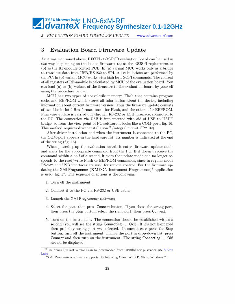
MCU has two types of nonvolatile memory: Flash that contains programcode, and EEPROM which stores all information about the device, includinginformation about current firmware version. Thus the firmware update consistsof two files in Intel Hex format, one – for Flash, and the other – for EEPROM.Firmware update is carried out through RS-232 or USB interface, connected tothe PC. The connection via USB is implemented with aid of USB to UARTbridge, so from the view point of PC software it looks like a COM-port, fig. 16.This method requires driver installation 2 (integral circuit CP2102).
After driver installation and when the instrument is connected to the PC,the COM-port appears in the hardware list. Its number is indicated at the endof the string (fig. 16).
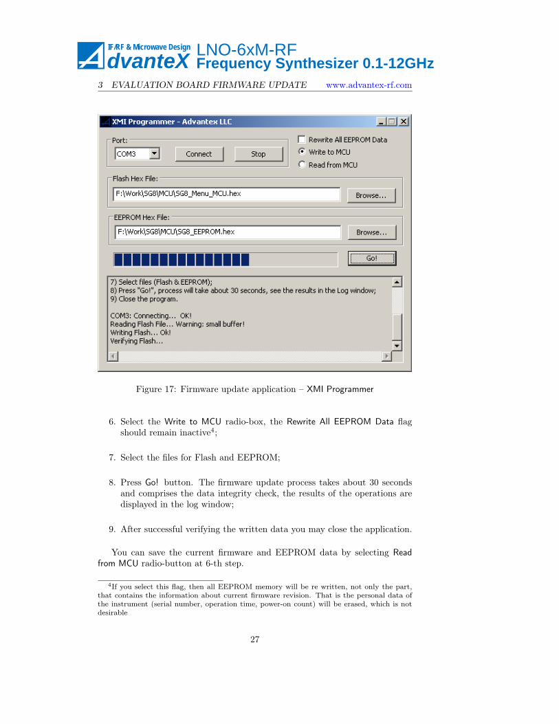
When powering up the evaluation board, it enters firmware update modeand waits for the appropriate command from the PC. If it doesn’t receive thecommand within a half of a second, it exits the update mode and no longer re-sponds to the read/write Flash or EEPROM commands, since in regular modeRS-232 and USB interfaces are used for remote control. For the firmware up-dating the XMI Programmer (XMEGA Instrument Programmer)3 applicationis used, fig. 17. The sequence of actions is the following:
1. Turn off the instrument;
2. Connect it to the PC via RS-232 or USB cable;
3. Launch the XMI Programmer software;
4. Select the port, then press Connect button. If you chose the wrong port,then press the Stop button, select the right port, then press Connect;
5. Turn on the instrument. The connection should be established within asecond (you will see the string Connecting. . . Ok!). If it’s not happenedthen probably wrong port was selected. In such a case press the Stopbutton, turn off the instrument, change the port in drop-down list, pressConnect and then turn on the instrument. The string Connecting. . . Ok!should be displayed;
2The driver (its last version) can be downloaded from CP2102 bridge vendor site SiliconLabs
3XMI Programmer software supports the following OSes: WinXP, Vista, Windows 7.
25
dvanteX LNO-6xM-RFFrequency Synthesizer 0.1-12GHz
IF/RF & Microwave Design
www.advantex-rf.com 3 EVALUATION BOARD FIRMWARE UPDATE
Figure 16: Device Manager window (My Computer .Manage)
26
dvanteX LNO-6xM-RFFrequency Synthesizer 0.1-12GHz
IF/RF & Microwave Design
3 EVALUATION BOARD FIRMWARE UPDATE www.advantex-rf.com
Figure 17: Firmware update application – XMI Programmer
6. Select the Write to MCU radio-box, the Rewrite All EEPROM Data flagshould remain inactive4;
7. Select the files for Flash and EEPROM;
8. Press Go! button. The firmware update process takes about 30 secondsand comprises the data integrity check, the results of the operations aredisplayed in the log window;
9. After successful verifying the written data you may close the application.
You can save the current firmware and EEPROM data by selecting Readfrom MCU radio-button at 6-th step.
4If you select this flag, then all EEPROM memory will be re written, not only the part,that contains the information about current firmware revision. That is the personal data ofthe instrument (serial number, operation time, power-on count) will be erased, which is notdesirable
27
dvanteX LNO-6xM-RFFrequency Synthesizer 0.1-12GHz
IF/RF & Microwave Design
www.advantex-rf.com 4 LNO-6XM SPI REGISTERS AND COMMANDS
4 LNO-6xM SPI Registers and Commands
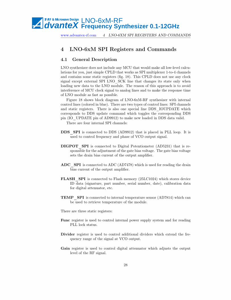
4.1 General Description
LNO synthesizer does not include any MCU that would make all low-level calcu-lations for you, just simple CPLD that works as SPI multiplexer 1-to-4 channelsand contains some static registers (fig. 18). This CPLD does not use any clocksignal except external SPI LNO_SCK line that changes its state only whenloading new data to the LNO module. The reason of this approach is to avoidinterference of MCU clock signal to analog lines and to make the response timeof LNO module as fast as possible.
Figure 18 shows block diagram of LNO-6xM-RF synthesizer with internalcontrol lines (colored in blue). There are two types of control lines: SPI channelsand static registers. There is also one special line DDS_IOUPDATE whichcorresponds to DDS update command which toggles the corresponding DDSpin (IO_UPDATE pin of AD9912) to make new loaded in DDS data valid.
There are four internal SPI channels:
DDS_SPI is connected to DDS (AD9912) that is placed in PLL loop. It isused to control frequency and phase of VCO output signal.
DIGPOT_SPI is connected to Digital Potentiometer (AD5231) that is re-sponsible for the adjustment of the gate bias voltage. The gate bias voltagesets the drain bias current of the output amplifier.
ADC_SPI is connected to ADC (AD7478) which is used for reading the drainbias current of the output amplifier.
FLASH_SPI is connected to Flash memory (25LC1024) which stores deviceID data (signature, part number, serial number, date), calibration datafor digital attenuator, etc.
TEMP_SPI is connected to internal temperature sensor (AD7814) which canbe used to retrieve temperature of the module.
There are three static registers:
Func register is used to control internal power supply system and for readingPLL lock status.
Divider register is used to control additional dividers which extend the fre-quency range of the signal at VCO output.
Gain register is used to control digital attenuator which adjusts the outputlevel of the RF signal.
28

dvanteX LNO-6xM-RFFrequency Synthesizer 0.1-12GHz
IF/RF & Microwave Design
4 LNO-6XM SPI REGISTERS AND COMMANDS www.advantex-rf.com
PFD
CP
+ -
REF
InV
CO
6-12
GH
zD
ivid
er1/
2N
1/12
OU
TPU
T_E
N(F
unc)
RF
Out
0.1-
12G
Hz
Gat
e Bi
as
Vol
tage
DD
S(A
D99
12)
Dig
ital
Pot
entio
met
er(A
D52
31)
Flas
h M
emor
y(2
5LC
1024
)
DIG
PO
T_SP
I
FLA
SH
_SP
I
TEM
P_S
PI
(Div
ider
)
DD
S_I
OU
PD
ATE
(0x1
1 co
mm
and)
DD
S_P
WR
_ON
(Fun
c)
InternalPower Supply
System
PO
WE
R_O
N(F
unc)
LNO-CTL(CPLD)
XL95
144X
L DD
S_SP
IC
TL_S
PIS
PI
DIG
PO
T_SP
I
FLA
SH_S
PI
TEM
P_SP
I
Func
Div
ider
Gai
n
DD
S_I
OU
PD
ATE
(Fun
c)
(Fun
c)
DD
S_S
PI
SPI Control & Power Supply
Connector
SP
I bus
Sta
tic li
nes.
Bit
nam
es a
re s
how
n w
ith u
pper
case
lette
rs, r
egis
ter n
ames
are
sho
wn
in p
aren
thes
esS
tatic
line
(1-b
it lin
e)
(Gai
n)
LOC
K(F
unc)
LOC
K
AD
C_S
PI
AD
C_S
PI
AD
C(A
D74
78)
Cur
rent
M
onito
r
Dra
in B
ias
Volta
ge(O
utpu
t Sta
geP
ower
Sup
ply)
For t
est a
nd de
bugg
ing
purp
oses
only
(not
used
in no
rmal
oper
ation
)
Tem
pera
ture
S
enso
r(A
D78
14)
Figure 18: LNO synthesizer block diagram
29

dvanteX LNO-6xM-RFFrequency Synthesizer 0.1-12GHz
IF/RF & Microwave Design
www.advantex-rf.com 4 LNO-6XM SPI REGISTERS AND COMMANDS
MSB LSB
SCK
MOSI
SS# 1-st bit
Time
Figure 19: LNO SPI writing cycle diagram
Command Byte 1-st Data Byte Last Data Byte
MSB LSBС6 С5 С4 С0С1С2С3 D0D1D2D3D4D5D6D7С7
Figure 20: Command and data bytes
4.2 Format of SPI Commands
LNO SPI commands consist of one command byte C[7:0] following by N databytes. Number of data bytes (N) depends on the particular command. Dataon LNO_MOSI signal line are latched on rising edge of LNO_SCK signal asshown on figure 19. MSB (Most Significant Bit) is loaded first, LSB (LeastSignificant Bit) – last. The first is the command byte C[7:0] all other bytesare data (fig. 20). The command byte works as the address for multiplexerimplemented in CPLD and defines the destination where to transfer followingdata – to one of the SPI channels or to one of the static registers, and the typeof operation – writing or reading.
At reading cycle data on LNO_MISO line are switched on the falling edge ofLNO_SCK signal and should be latched by master on rising edge of LNO_SCKsignal accordingly as shown in figure 21.
C7
SCK
C6 C5 C4 C3 C2 C1 C0MOSI
SS#
MISO Dn Dn-1 D4 D3 D2 D1 D0
Figure 21: LNO SPI reading cycle diagram
30
dvanteX LNO-6xM-RFFrequency Synthesizer 0.1-12GHz
IF/RF & Microwave Design
4 LNO-6XM SPI REGISTERS AND COMMANDS www.advantex-rf.com
Command Data
MSB LSBС6 С5 С4 С0С1С2С3С7 D0D1D2D3D4D5D6D7
Figure 22: Writing 1 data byte
4.3 SPI Commands
Table 2 shows commands C[7:0] used to control LNO module.
4.3.1 Func register writing C[7:0]=0x01
This command writes 1 data byte D[7:0] to Func register (fig. 22). Table 3shows the meaning of these data bits.
4.3.2 Func register reading C[7:0]=0x81
This command reads the content of Func register. See table 3 and figure 21 formore details.
4.3.3 Divider buffer register writing C[7:0]=0x02
This command writes 1 data byte D[7:0] to Divider buffer register (fig. 22). Itdefines the division factor of VCO output signal. VCO frequency range is from6 to 12 GHz, so to obtain any other frequency which is lower than 6 GHz youneed to divide VCO frequency. To cover all range from 100 MHz to 12 GHzoutput dividers with 2N division factors are used (fig. 18). Table 4 shows themeaning of data bits controlling these output dividers.
4.3.4 Divider buffer register reading C[7:0]=0x82
This command reads the content of Divider register. See table 4 and figure 21for more details.
4.3.5 Gain buffer register writing C[7:0]=0x03
This command writes 1 data byte D[7:0] to Gain buffer register (fig. 22). Itis used to control digital attenuator which adjusts the output level of the RFsignal. Approximately the output level in dBm is defined by the following: Out-put Level = 15−Attenuation. Minimum attenuation corresponds to maximumoutput level. Table 5 shows register values and corresponding attenuation.
31

dvanteX LNO-6xM-RFFrequency Synthesizer 0.1-12GHz
IF/RF & Microwave Design
www.advantex-rf.com 4 LNO-6XM SPI REGISTERS AND COMMANDS
Table 2: LNO SPI Commands C[7:0]C[7:0] #
ofbytes
Description
1 0x01 1 Writing to Func register. This command changes thestates of static lines
2 0x81 1 Reading from Func register3 0x02 1 Writing to Divider buffer register (without changes of
the states of static lines)4 0x82 1 Reading from Divider buffer register5 0x03 1 Writing to Gain buffer register (without changes of the
states of static lines)6 0x83 1 Reading from Gain buffer register7 0x04 1 Writing to DigPotWP register. This command changes
the states of static lines8 0x84 1 Reading from DigPotWP register9 0x05 1 Writing to internal MuxOut register10 0x85 1 Reading from internal MuxOut register11 0x10 – Access to DDS_SPI (DDS AD9912)12 0x11 1 Toggling DDS IO_UPDATE signal (DDS AD9912)13 0x12 1 Updating Divider register. This command changes the
states of static lines according to the buffer registercontent loaded by 0x02 command
14 0x13 1 Updating Gain register. This command changes thestates of static lines according to the buffer register
content loaded by 0x02 command15 0x1F 1 Toggling DDS IO_UPDATE signal (DDS AD9912)
and updating Divider and Gain registers at one time16 0x30 2 Access to TEMP_SPI (Temperature Sensor AD7814)17 0x40 2 Access to ADC_SPI – current sensor ADC (AD7478)18 0x50 3 Access to DIGPOT_SPI – digital potentiometer
(AD5231)19 0x70 – Access to FLASH_SPI (Flash Memory 25LC1024)
32
dvanteX LNO-6xM-RFFrequency Synthesizer 0.1-12GHz
IF/RF & Microwave Design
4 LNO-6XM SPI REGISTERS AND COMMANDS www.advantex-rf.com
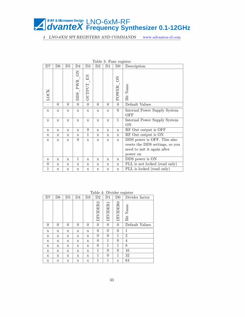
Table 3: Func registerD7 D6 D5 D4 D3 D2 D1 D0 Description
LOCK
DDS_
PW
R_ON
OUTPUT_EN
POW
ER_ON
BitNam
e
– 0 0 0 0 0 0 0 Default Valuesx x x x x x x 0 Internal Power Supply System
OFFx x x x x x x 1 Internal Power Supply System
ONx x x x 0 x x x RF Out output is OFFx x x x 1 x x x RF Out output is ONx x x 0 x x x x DDS power is OFF. This also
resets the DDS settings, so youneed to init it again afterpower on
x x x 1 x x x x DDS power is ON0 x x x x x x x PLL is not locked (read only)1 x x x x x x x PLL is locked (read only)
Table 4: Divider registerD7 D6 D5 D4 D3 D2 D1 D0 Divider factor
DIV
IDER2
DIV
IDER1
DIV
IDER0
BitNam
e
0 0 0 0 0 0 0 0 Default Valuesx x x x x 0 0 0 1x x x x x 0 0 1 2x x x x x 0 1 0 4x x x x x 0 1 1 8x x x x x 1 0 0 16x x x x x 1 0 1 32x x x x x 1 1 x 64
33

dvanteX LNO-6xM-RFFrequency Synthesizer 0.1-12GHz
IF/RF & Microwave Design
www.advantex-rf.com 4 LNO-6XM SPI REGISTERS AND COMMANDS
Table 5: Gain registerD7 D6 D5 D4 D3 D2 D1 D0 Attenuation, dB
GAIN
5
GAIN
4
GAIN
3
GAIN
2
GAIN
1
GAIN
0
BitNam
e
0 0 0 0 0 0 0 0 Default Valuesx x 0 0 0 0 0 0 31.5x x 0 0 0 0 0 1 31x x 0 0 0 0 1 0 30
...x x 1 1 1 1 1 0 0.5x x 1 1 1 1 1 1 0
Table 6: DigPotWP registerD7 D6 D5 D4 D3 D2 D1 D0 Attenuation, dB
WP#
BitNam
e
0 0 0 0 0 0 0 0 Default Valuesx x x x x x x 0 Write operation protectedx x x x x x x 1 Write operation is allowed
4.3.6 Gain buffer register reading C[7:0]=0x83
This command reads the content of Gain buffer register. See table 5 and figure21 for more details.
4.3.7 DigPotWP register writing C[7:0]=0x04
This command writes 1 data byte D[7:0] to DigPotWP register (fig. 22). Itallows or denies the write operation to the digital potentiometer (table 6) whichsets the gate bias voltage of the output amplifier.
4.3.8 DigPotWP register reading C[7:0]=0x84
This command reads the content of DigPotWP register. See table 6 and figure21 for more details.
4.3.9 MuxOut register writing C[7:0]=0x05
This command writes 1 data byte D[7:0] to MuxOut register (fig. 22). Thisregister defines the behaviour of the LNO_AUX output signal (table 7).
34

dvanteX LNO-6xM-RFFrequency Synthesizer 0.1-12GHz
IF/RF & Microwave Design
4 LNO-6XM SPI REGISTERS AND COMMANDS www.advantex-rf.com
Table 7: MuxOut registerD7 D6 D5 D4 D3 D2 D1 D0 Attenuation, dB
FUNC_IN
T_EN
DIV
N_IN
T_EN
GAIN
_IN
T_EN
DDS_
UPD_IN
T_EN
MUX1
MUX0
BitNam
e0 0 0 0 0 0 0 0 Default Valuesx x x x x x 0 0 LNO_AUX<=’0’x x x x x x 0 1 LNO_AUX<=LOCKx x x x x x 1 0 LNO_AUX<=UPDATEx x x x x x 1 1 LNO_AUX<=’1’0 x x x x x 1 0 Disable the toggling of UPDATE signal
when Func register is loaded1 x x x x x 1 0 Enable the toggling of UPDATE signal
when Func register is loaded with newdata
x 0 x x x x 1 0 Disable the toggling of UPDATE signalwhen Divider static lines are updated
x 1 x x x x 1 0 Enable the toggling of UPDATE signalwhen Divider static lines are updated
x x 0 x x x 1 0 Disable the toggling of UPDATE signalwhen Gain static lines are updated
x x 1 x x x 1 0 Enable the toggling of UPDATE signalwhen Gain static lines are updated
x x x 0 x x 1 0 Disable the toggling of UPDATE signalwhen DDS_IOUPDATE signal istoggling
x x x 1 x x 1 0 Enable the toggling of UPDATE signalwhen DDS_IOUPDATE signal istoggling
35

dvanteX LNO-6xM-RFFrequency Synthesizer 0.1-12GHz
IF/RF & Microwave Design
www.advantex-rf.com 4 LNO-6XM SPI REGISTERS AND COMMANDS
D[1:0]=”01” LNO_AUX output signal is connected to internal LOCK signalwhich indicates PLL lock status.
D[1:0]=”10” LNO_AUX output signal is connected to internal UPDATE signalwhich indicates the update process of the static lines of Func, Di-vider, Gain registers and also it can indicate the toggling of DDS_IOUPDATEsignal. The behaviour of UPDATE signal depends on D[7:4] flag bits.UPDATE signal can be used to observe transient process at RF out-put just after loading new data to the synthesizer. For example itcan be used when measuring the frequency or level switching time.UPDATE signal switches from low to high state at rising edge ofLNO_SCK signal at the same time as the static control lines (Func,Divider, Gain etc.) switch to their new states. UPDATE signalswitches from high to low at rising edge of LNO_CS# signal.
4.3.10 MuxOut register reading C[7:0]=0x85
This command reads the content of MuxOut register. See table 7 and figure 21for more details.
4.3.11 DDS_SPI Access C[7:0]=0x10
This command is used to access the DDS (AD9912) controlling phase and fre-quency of VCO output signal. Number of data bytes can be different but notless than 3 bytes. Actual length of data is defined in first 2 data bytes (LongInstruction). For more information refer to section 5 and AD9912 data sheet.
4.3.12 Toggling DDS_IOUPDATE C[7:0]=0x11
After the loading new data to DDS you need to toggle DDS_IOUPDATE signalby sending this command to SPI. It is required for DDS proper operation (seeAD9912 data sheet).
4.3.13 Divider register updating C[7:0]=1x12
This command updates the control static signals which correspond to Dividerbuffer register.
4.3.14 Gain register updating C[7:0]=1x13
This command updates the control static signals which correspond to Gainbuffer register.
4.3.15 All register updating and DDS_IOUPDATE toggling C[7:0]=1x1F
This command updates the control static signals which correspond to Dividerand Gain buffer registers and toggles DDS_IOUPDATE signal.
36

dvanteX LNO-6xM-RFFrequency Synthesizer 0.1-12GHz
IF/RF & Microwave Design
5 LNO-6XM SPI PROGRAMMING www.advantex-rf.com
4.3.16 TEMP_SPI Access C[7:0]=0x30
This command is used to access the temperature detector (AD7814) locatednear DDS IC. This command uses 2 data bytes D[15:0]. For more informationrefer to section 5 and AD7814 data sheet.
4.3.17 ADC_SPI Access C[7:0]=0x40
This command is used to access the ADC (AD7478) to read the drain biascurrent value. Rated drain bias current is 75mA. ADC reference voltage is3.3V. Measured drain current ID is converted to the input ADC voltage VADC
as follows: VADC = 20 · ID · R, where R=1 Ohm. Thus ADC code in normaloperation should be about 1862 (full scale corresponds to 212). This commanduses 2 data bytes D[15:0]. For more information refer to section 5 and AD7478data sheet.
4.3.18 DIGPOT_SPI Access C[7:0]=0x50
This command is used to access to the digital potentiometer (AD5231) to adjustgate bias voltage which in turn defines drain bias current of the output amplifier.The digital potentiometer has 0 to 1023 range, 0 corresponds to the maximumdrain current, 1023 corresponds to the minimum current. After adjusting thecurrent, write the adjusted digital potentiometer value to its flash memory.This code will be loaded at power on automatically, so you won’t need to accessto ADC or Digital Potentiometer anymore. This command uses 3 data bytesD[23:0]. For more information refer to section 5 and AD5231 data sheet.
4.3.19 FLASH_SPI Access C[7:0]=0x70
This command is used to access to the flash memory of LNO module whichstores product ID, serial number, calibration data etc. For more informationrefer to section 5 and 25LC1024 data sheet.
5 LNO-6xM SPI Programming
5.1 Parameter CalculationsWorking with synthesizer implies some calculation procedure that should beimplemented on the user side. It includes algorithms of DDS FTW registervalue and Divider register value calculations based on the input frequency. Formore precise output level setting you can also use Gain register value calculationsbased on the calibration data stored in the flash memory of the module.
Thus we have some input parameters in user friendly format (e.g. frequency,phase, level as float numbers), some calibration data stored in flash memoryembedded to the module, and as a result of calculation algorithms – output datain low-level format (i.e. register values), see figure 23. This section describeshow to find these output parameters.
37

dvanteX LNO-6xM-RFFrequency Synthesizer 0.1-12GHz
IF/RF & Microwave Design
www.advantex-rf.com 5 LNO-6XM SPI PROGRAMMING
Input parameters
(Frequency, Phase,
Level, etc.)Calculation
algorithms
Calibration
Data
Output parameters
(LNO register values)
Figure 23: Input and output data for LNO programming
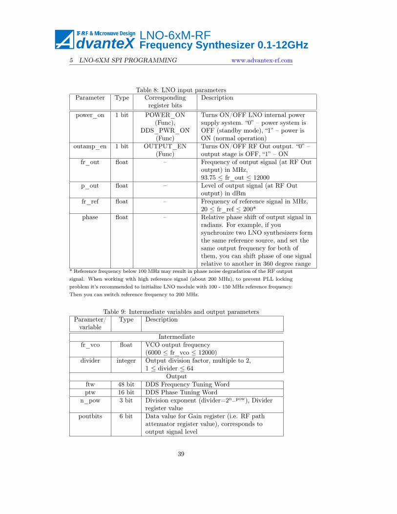
Table 8 shows input parameters. Some of them are in ready-to-use format,like power_on, outamp_en, other can not be loaded to LNO directly. Table 9shows intermediate variables used in calculation algorithms, table shows outputparameters which are downloaded to LNO registers.
n_pow
n_pow = floor(log(6000.0/fr_out)/log(2))+1
divider
divider = 2^n_pow (2 to the n_power)
fr_vco
fr_vco = fr_out*divider
ftw
ftw = round((3*2^50)*fr_ref/fr_vco)
ptw
ptw = round((2^16)*phase*fr_ref/(2π*fr_out))
poutbits
For the approximate output level setting you can use the following equation.
poutbits = round(2*(p_out+16))
For more precise output level setting you can also use Gain register value calcu-lations based on the calibration data stored in the flash memory of the module.The calculation of poutbits is based on the calibration values (Gain values)residing on 2-dimensional rectilinear grid (frequency and level). To find Gainvalue (i.e. poutbits value) for the arbitrary frequency-level point, bilinear in-terpolation can be used. Calibration data is retrieved from the flash memory –table CTYPE=8, for more details see section 5.5. Suppose that we have four
38
dvanteX LNO-6xM-RFFrequency Synthesizer 0.1-12GHz
IF/RF & Microwave Design
5 LNO-6XM SPI PROGRAMMING www.advantex-rf.com
Table 8: LNO input parametersParameter Type Corresponding
register bitsDescription
power_on 1 bit POWER_ON(Func),
DDS_PWR_ON(Func)
Turns ON/OFF LNO internal powersupply system. “0” – power system isOFF (standby mode), “1” – power isON (normal operation)
outamp_en 1 bit OUTPUT_EN(Func)
Turns ON/OFF RF Out output. “0” –output stage is OFF, “1” – ON
fr_out float – Frequency of output signal (at RF Outoutput) in MHz,93.75 ≤ fr_out ≤ 12000
p_out float – Level of output signal (at RF Outoutput) in dBm
fr_ref float – Frequency of reference signal in MHz,20 ≤ fr_ref ≤ 200*
phase float – Relative phase shift of output signal inradians. For example, if yousynchronize two LNO synthesizers formthe same reference source, and set thesame output frequency for both ofthem, you can shift phase of one signalrelative to another in 360 degree range
* Reference frequency below 100 MHz may result in phase noise degradation of the RF outputsignal. When working with high reference signal (about 200 MHz), to prevent PLL lockingproblem it’s recommended to initialize LNO module with 100 - 150 MHz reference frequency.Then you can switch reference frequency to 200 MHz.
Table 9: Intermediate variables and output parametersParameter/variable
Type Description
Intermediatefr_vco float VCO output frequency
(6000 ≤ fr_vco ≤ 12000)divider integer Output division factor, multiple to 2,
1 ≤ divider ≤ 64Output
ftw 48 bit DDS Frequency Tuning Wordptw 16 bit DDS Phase Tuning Word
n_pow 3 bit Division exponent (divider=2n_pow), Dividerregister value
poutbits 6 bit Data value for Gain register (i.e. RF pathattenuator register value), corresponds tooutput signal level
39

dvanteX LNO-6xM-RFFrequency Synthesizer 0.1-12GHz
IF/RF & Microwave Design
www.advantex-rf.com 5 LNO-6XM SPI PROGRAMMING
Q11
Q21
Q22
Q12 R1
R2
P
X (Frequency)
Z (Level)
Y (RF Path Attenuator Register Value)
Figure 24: Bilinear interpolation
calibration points (Q11, Q12, Q21, Q22) around the point which Gain value weneed to find (P ), see fig 24. X axis means frequency in MHz, Z axis – out-put level in dBm, Y – Gain value. So we have Q11 = (x1, z1), Q12 = (x1, z2),Q21 = (x2, z1), Q22 = (x2, z2), P = (x, z), Y (Q11), Y (Q12), Y (Q21), Y (Q22) –are calibration values, and we need to find Y (P ).
First we need to find Y values of auxiliary points R1 and R2, where R1 =(x, z1) and R2 = (x, z2):
Y (R1) ≈x2 − x
x2 − x1Y (Q11) +
x− x1
x2 − x1Y (Q21)
Y (R2) ≈x2 − x
x2 − x1Y (Q12) +
x− x1
x2 − x1Y (Q22)
Then we need to find interpolated value between auxiliary points R1 andR2:
Y (P ) =z2 − z
z2 − z1Y (R1) +
z − z1z2 − z1
Y (R2).
Gain register maximum value (0x3F) corresponds to maximum output level,value 0x00 – corresponds to minimum signal level at RF Out output, LSB ofGain register is about 0.5 dB.
5.2 Initialization
After power on the LNO synthesizer is in standby mode, i.e. internal powersupply system is off, and DDS, Gain, Divider and other registers are in theirdefault state. So just after power on you need to initialize it by the followingprocedure:
1. Set minimum output signal level by loading to SPI 0x0300.
40

dvanteX LNO-6xM-RFFrequency Synthesizer 0.1-12GHz
IF/RF & Microwave Design
5 LNO-6XM SPI PROGRAMMING www.advantex-rf.com
Table 10: Turning on the internal power supply system at initialization processC[7:0] D7 D6 D5 D4 D3 D2 D1 D0
– – – dds_
pwr_
on
output_en
power_on
0x01 0 0 0 0 1 0 0 1
Table 11: Turning on the DDS power supply at initialization processC[7:0] D7 D6 D5 D4 D3 D2 D1 D0
– – – dds_
pwr_
on
output_en
power_on
0x01 0 0 0 1 1 0 0 1
2. Turn on the internal power supply by loading to SPI value shown in table10.
3. Turn on the DDS power supply by loading to SPI value shown in table11. Turning on the DDS power supply as separate operation is requiredfor all power supply voltages were settled before DDS power-on.
4. Reset the DDS – 0x10001201
5. Update DDS – 0x1100 (toggle DDS_IOUPDATE signal)
6. Initialize DDS:
(a) 0x10000080 (write to DDS at address 0x0000)
(b) 0x10001090 (write to DDS at address 0x0010)
(c) 0x10040BFF (write to DDS at address 0x040B)
(d) 0x10040C03 (write to DDS at address 0x040C)
7. Update DDS and Gain register – 0x1F00
5.3 Setting Frequency, Phase and Level
To set level and frequency at one time use the following command sequence:
1. 0х1061AB[ftw] (setting frequency)
41

dvanteX LNO-6xM-RFFrequency Synthesizer 0.1-12GHz
IF/RF & Microwave Design
www.advantex-rf.com 5 LNO-6XM SPI PROGRAMMING
2. 0x020[’0’][n_pow] (Divider register)
3. 0х03[“00”][poutbits] (setting output level)
4. 0x1F00 (update all control static lines and toggle DDS_IOUPDATE)
To set only level use the following command sequence:
1. 0х03[“00”][poutbits] (setting output level)
2. 0x1300 (update Gain static lines)
To set only frequency (without output level correction) use the following com-mand sequence:i It should be noted that when
you set new frequency, the output
level can be slightly different from
the level at previous frequency. For
large frequency step it’s
recommended to recalculate poutbits
for new frequency for output level
correction
1. 0х1061AB[ftw] (setting frequency)
2. 0x020[’0’][n_pow] (Divider register)
3. 0x1F00 (update all control static lines and toggle DDS_IOUPDATE)
To set new phase of output signal you need to load the following:
1. 0х1061AD[ptw]
2. 0x1100 (toggle DDS_IOUPDATE)
For the PLL to remain in locked condition, it’s good idea to set new phase byseveral small phase shifts. Phase difference between old and new consecutivevalues should meet the following condition:
∆ptw
216� 1.
5.4 Reading internal temperatureTemperature detector (AD7814) embedded to LNO calculates temperature each350 us. Other times it resides in standby mode. If reading temperature rate isfaster than 350 us then detector is not able to calculate new temperature value,and you will read the same value. Thus it is recommended to read temperaturevalue not faster than one time per 500 us.
To read the temperature proceed as follows:
1. 0x300000 (sets normal operation of Temperature Detector)
2. Wait for 500 us
3. 0x30FFFF (sets Temperature Detector to power down mode and readstemperature code in format b00D[9:0]0000, where D is 10-bit signed in-teger). Temperature value in ºC can be found by the following equationT = 0.25 ·D.
For more details about Temperature Detector operation see AD7814 datasheet.
42

dvanteX LNO-6xM-RFFrequency Synthesizer 0.1-12GHz
IF/RF & Microwave Design
5 LNO-6XM SPI PROGRAMMING www.advantex-rf.com
FLASH_ADR FLASH_CMD DATA0 DATA1 DATAn
Figure 25: Structure of flash-memory data transfer
Table 12: Flash-memory commandsCommand Byte Description
FLASH_CMD_READ 0x03 Read dataFLASH_CMD_WRITE 0x02 Write dataFLASH_CMD_WREN 0x06 Write data enableFLASH_CMD_WRDI 0x04 Write data disableFLASH_CMD_RDSR 0x05 Read status registerFLASH_CMD_WRSR 0x01 Write status registerFLASH_CMD_PE 0x42 Page eraseFLASH_CMD_SE 0xD8 Byte eraseFLASH_CMD_CE 0xC7 Erase all
FLASH_CMD_RDID 0xAB Read ID and Turn on flash-memory Power SupplyFLASH_CMD_PDP 0xB9 Turn off flash-memory Power Supply
5.5 Flash MemoryLNO synthesizer has 1 Mbit (131072 bytes) Flash-memory. Its address spaceis within 0x00000 to 0x1FFFF range. Memory space is divided into pages, 256bytes each. It is possible to work with separate bytes and with pages. Pagesstart at addresses 0xXXX00, where XXX is in range 000 to 1FF. The numberof data bytes in packet can be different and depends on the actual memorycommand. General structure of the packet is shown in figure 25. First commandbyte, FLASH_ADR (0x70 – Flash-memory access, see table 2), is for CPLDmultiplexer, second byte is command for the 25LC1024 memory, followed bydata bytes if required. Flash-memory commands are listed in table 12.
5.5.1 FLASH_CMD_READ (0x03)
Data read command, see figure 26. First byte – FLASH_SPI access command
0x70 ADR2(MSB)0x03 ADR1 ADR0(LSB)
ANSWER
IN
OUT
Figure 26: Flash-memory data read command
43

dvanteX LNO-6xM-RFFrequency Synthesizer 0.1-12GHz
IF/RF & Microwave Design
www.advantex-rf.com 5 LNO-6XM SPI PROGRAMMING
0x70 ADR2(MSB)0x02 ADR1 ADR0(LSB) ANSWER0IN
ANSWER1 ANSWERn
Figure 27: Flash-memory data write command
0x70 0x06
IN
Figure 28: Flash-memory write enable command
for CPLDmultiplexer (0x70), second – flash data read command FLASH_CMD_READ(0x03), then three bytes which contains data address ADR[2:0]. Actually it’sstart address, so if you hold SS# signal in active position (“0”) you will getdata at next address for each CLK cycle. For example if we have the followingdata (3 bytes) 0xAA, 0xBB, 0xCC which are located at addresses 0x000006,0x000007 and 0x000008 respectively. To retrieve these three bytes at once weneed to send the following command: 0x0703000006000000. Last three zerobytes in this command are used to generate CLK cycles to retrieve three con-secutive data bytes. As a response on MISO line we will obtain the following:0xAABBCC.
5.5.2 FLASH_CMD_WRITE (0x02)
Data write command, see figure 27. First byte – FLASH_SPI access commandfor CPLDmultiplexer (0x70), second – flash data write command FLASH_CMD_WRITE(0x02), then three address bytes ADR[2:0] and data bytes. First data byte willbe written at ADR[2:0] address, second at ADR[2:0]+1 and so on, but all writ-ten data should reside inside the same page. This way maximum number ofdata bytes is 256 if ADR[2:0] points to the start of page. Otherwise if addressADR[2:0] plus number of bytes exceeds the address of end of page, some dataof this page will be overwritten. This will result in lost of some data.
5.5.3 FLASH_CMD_WREN (0x06)
Write enable command, see figure 28. This command sets WEL bit to “1” inflash-memory status register. To enable any write or erase operation, this bitshould be set to “1”, otherwise these operations won’t be performed. WEL bitis reset automatically to “0” after performing the following commands:
• FLASH_CMD_WRDI
• FLASH_CMD_WRSR
• FLASH_CMD_WRITE
• FLASH_CMD_PE
44

dvanteX LNO-6xM-RFFrequency Synthesizer 0.1-12GHz
IF/RF & Microwave Design
5 LNO-6XM SPI PROGRAMMING www.advantex-rf.com
0x70 0x04
IN
Figure 29: Flash-memory write/erase disable command
0x70 0x05
ANSWER
IN
OUT
Figure 30: Flash-memory status register reading
• FLASH_CMD_SE
• FLASH_CMD_CE
After power on WEL bit is also in “0” state.
5.5.4 FLASH_CMD_WRDI (0x04)
This command disables write and erase operations by setting WEL bit to “0” instatus register of flash-memory. Command is shown in figure 29.
5.5.5 FLASH_CMD_RDSR (0x05)
This command reads flash-memory status register, see figure 30. Table 13 showsthe content of status register.
WIP – flash-memory busy. “1” – write operation in progress (is not finished).“0” – all operations are finished.
WEL – write enable. “0” – write/erase operation disabled, “1” – enabled.
BP1, BP0 – memory block write protection. All address space is divided into4 blocks and these bits can be used to control protection for write/eraseoperations for these blocks, see table 14.
To perform reading operation you need to send 0x700500.
Table 13: Flash-memory status registerR7 R6 R5 R4 R3 R2 R1 R0
Read/Write – – – – R/W R/W R RX X X X BP1 BP0 WEL WIP
45

dvanteX LNO-6xM-RFFrequency Synthesizer 0.1-12GHz
IF/RF & Microwave Design
www.advantex-rf.com 5 LNO-6XM SPI PROGRAMMING
Table 14: Flash-memory block protectionBP1 BP0 Protected area Unprotected area0 0 – All address area
(00000h-1FFFFh)0 1 Upper 1/4 address space
(18000h–1FFFFh)Lower 3/4 address space
(00000h-17FFFh)1 0 Upper 1/2 address space
(10000h-1FFFFh)Lower 1/2 address space
(00000h-0FFFFh)1 1 All address space
(00000h-1FFFFh)–
0x70 0x01
INDATA
Figure 31: Flash-memory write to status register
5.5.6 FLASH_CMD_WRSR (0x01)
Write to status register, figure 31. Actually this command is used to set BP0and BP1 bits, since WEL bit can be controlled via FLASH_CMD_WREN andFLASH_CMD_WRDI commands.
5.5.7 FLASH_CMD_PE (0x42)
Command erases content of a page which address is inserted in command, seefigure 32.
5.5.8 FLASH_CMD_SE (0xD8)
Clears one byte, figure 33.
5.5.9 FLASH_CMD_CE (0xC7)
Clears all memory, figure 34.
5.5.10 FLASH_CMD_RDID (0xAB)
This command turns on the memory power supply and reads ID number of thechip (ID=0x29), figure 35. To perform reading you should send 0x70AB00, and
0x70 ADR2(MSB)0x42 ADR1 ADR0(LSB)IN
Figure 32: Flash-memory page erase command
46

dvanteX LNO-6xM-RFFrequency Synthesizer 0.1-12GHz
IF/RF & Microwave Design
5 LNO-6XM SPI PROGRAMMING www.advantex-rf.com
0x70 ADR2(MSB)0xD8 ADR1 ADR0(LSB)IN
Figure 33: Flash-memory byte erase command
0x70 0xC7
IN
Figure 34: Flash-memory clear all command
you get 0x29 in response.
5.5.11 FLASH_CMD_PDP (0xB9)
Turns off the memory chip power supply, see figure 36.
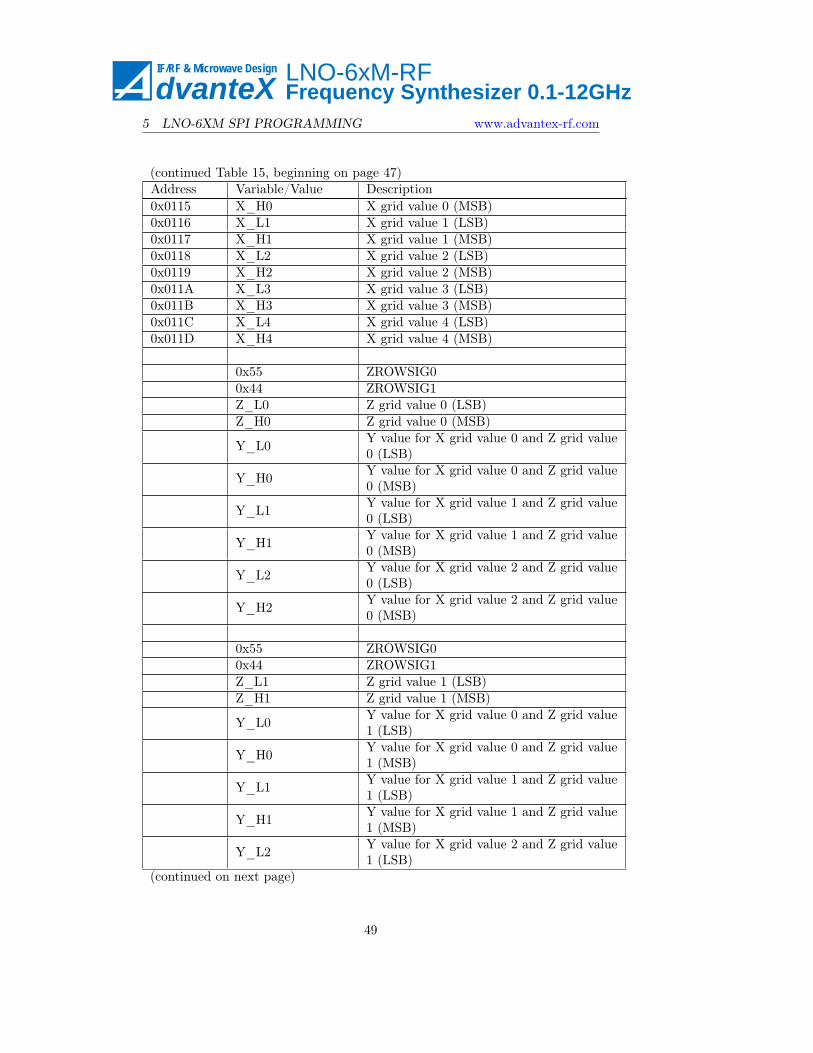
5.6 Memory address and data mappingAddress and data mapping is shown in table 15.
Table 15: Memory address and data mapping
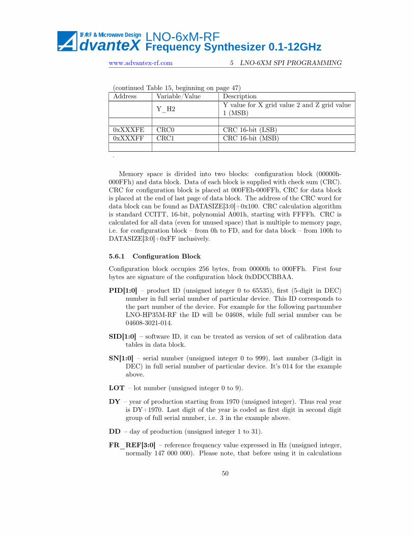
Address Variable/Value Description0x00 0xAA CONFIGBLKSIG00x01 0xBB CONFIGBLKSIG10x02 0xCC CONFIGBLKSIG20x03 0xDD CONFIGBLKSIG30x04 PID0 Product ID (LSB)0x05 PID1 Product ID (MSB)0x06 SID0 Software ID (LSB)0x07 SID1 Software ID (MSB)0x08 SN0 Serial Number (LSB)0x09 SN1 Serial Number (MSB)0x0A LOT Lot0x0B DY Year of production(continued on next page)
0x70 0xAB
IN
ANSWER
OUT
Figure 35: Flash-memory power on and read ID command
47

dvanteX LNO-6xM-RFFrequency Synthesizer 0.1-12GHz
IF/RF & Microwave Design
www.advantex-rf.com 5 LNO-6XM SPI PROGRAMMING
(continued Table 15, beginning on page 47)Address Variable/Value Description0x0C DM Month of of production0x0D DD Day of production
0x10 REF_FR0 Reference frequency in Hz (LSB)0x11 REF_FR1 Reference frequency in Hz0x12 REF_FR2 Reference frequency in Hz0x13 REF_FR3 Reference frequency in Hz (MSB)0x14 DATA_SIZE0 Size of Data Block (LSB)0x15 DATA_SIZE1 Size of Data Block0x16 DATA_SIZE2 Size of Data Block0x17 DATA_SIZE3 Size of Data Block (MSB)0x18 FLASH_SIZE0 Flash-memory size (LSB) = 0x000x19 FLASH_SIZE1 Flash-memory size = 0x000x1A FLASH_SIZE2 Flash-memory size = 0x000x1B FLASH_SIZE3 Flash-memory size (MSB) = 0x02
0x00FE CRC0 CRC 16-bit (LSB)0x00FF CRC1 CRC 16-bit (MSB)
0x0100(0xXXX00) 0x99 TABLESIG0
0x0101 0x88 TABLESIG10x0102 0x77 TABLESIG20x0103 0x66 TABLESIG30x0104 CTYPE Table type (characteristic type)0x0105 XVALUE Type of X axis values0x0106 YVALUE Type of Y axis values0x0107 ZVALUE Type of Z axis values0x0108 ZCOUNT0 Number of points on Z axis (LSB)0x0109 ZCOUNT1 Number of points on Z axis0x010A ZCOUNT2 Number of points on Z axis0x010B ZCOUNT3 Number of points on Z axis (MSB)0x010C XYCOUNT0 Number of points on X axis (LSB)0x010D XYCOUNT1 Number of points on X axis0x010E XYCOUNT2 Number of points on X axis0x010F XYCOUNT3 Number of points on X axis (MSB)0x0110 0x33 XROWSIG00x0111 0x22 XROWSIG10x0112 X_MULT X multiplier0x0113 – Not used0x0114 X_L0 X grid value 0 (LSB)(continued on next page)
48
dvanteX LNO-6xM-RFFrequency Synthesizer 0.1-12GHz
IF/RF & Microwave Design
5 LNO-6XM SPI PROGRAMMING www.advantex-rf.com
(continued Table 15, beginning on page 47)Address Variable/Value Description0x0115 X_H0 X grid value 0 (MSB)0x0116 X_L1 X grid value 1 (LSB)0x0117 X_H1 X grid value 1 (MSB)0x0118 X_L2 X grid value 2 (LSB)0x0119 X_H2 X grid value 2 (MSB)0x011A X_L3 X grid value 3 (LSB)0x011B X_H3 X grid value 3 (MSB)0x011C X_L4 X grid value 4 (LSB)0x011D X_H4 X grid value 4 (MSB)
0x55 ZROWSIG00x44 ZROWSIG1Z_L0 Z grid value 0 (LSB)Z_H0 Z grid value 0 (MSB)
Y_L0 Y value for X grid value 0 and Z grid value0 (LSB)
Y_H0 Y value for X grid value 0 and Z grid value0 (MSB)
Y_L1 Y value for X grid value 1 and Z grid value0 (LSB)
Y_H1 Y value for X grid value 1 and Z grid value0 (MSB)
Y_L2 Y value for X grid value 2 and Z grid value0 (LSB)
Y_H2 Y value for X grid value 2 and Z grid value0 (MSB)
0x55 ZROWSIG00x44 ZROWSIG1Z_L1 Z grid value 1 (LSB)Z_H1 Z grid value 1 (MSB)
Y_L0 Y value for X grid value 0 and Z grid value1 (LSB)
Y_H0 Y value for X grid value 0 and Z grid value1 (MSB)
Y_L1 Y value for X grid value 1 and Z grid value1 (LSB)
Y_H1 Y value for X grid value 1 and Z grid value1 (MSB)
Y_L2 Y value for X grid value 2 and Z grid value1 (LSB)
(continued on next page)
49
dvanteX LNO-6xM-RFFrequency Synthesizer 0.1-12GHz
IF/RF & Microwave Design
www.advantex-rf.com 5 LNO-6XM SPI PROGRAMMING
(continued Table 15, beginning on page 47)Address Variable/Value Description
Y_H2 Y value for X grid value 2 and Z grid value1 (MSB)
0xXXXFE CRC0 CRC 16-bit (LSB)0xXXXFF CRC1 CRC 16-bit (MSB)
.
Memory space is divided into two blocks: configuration block (00000h-000FFh) and data block. Data of each block is supplied with check sum (CRC).CRC for configuration block is placed at 000FEh-000FFh, CRC for data blockis placed at the end of last page of data block. The address of the CRC word fordata block can be found as DATASIZE[3:0]+0x100. CRC calculation algorithmis standard CCITT, 16-bit, polynomial A001h, starting with FFFFh. CRC iscalculated for all data (even for unused space) that is multiple to memory page,i.e. for configuration block – from 0h to FD, and for data block – from 100h toDATASIZE[3:0]+0xFF inclusively.
5.6.1 Configuration Block
Configuration block occupies 256 bytes, from 00000h to 000FFh. First fourbytes are signature of the configuration block 0xDDCCBBAA.
PID[1:0] – product ID (unsigned integer 0 to 65535), first (5-digit in DEC)number in full serial number of particular device. This ID corresponds tothe part number of the device. For example for the following partnumberLNO-HP35M-RF the ID will be 04608, while full serial number can be04608-3021-014.
SID[1:0] – software ID, it can be treated as version of set of calibration datatables in data block.
SN[1:0] – serial number (unsigned integer 0 to 999), last number (3-digit inDEC) in full serial number of particular device. It’s 014 for the exampleabove.
LOT – lot number (unsigned integer 0 to 9).
DY – year of production starting from 1970 (unsigned integer). Thus real yearis DY+1970. Last digit of the year is coded as first digit in second digitgroup of full serial number, i.e. 3 in the example above.
DD – day of production (unsigned integer 1 to 31).
FR_REF[3:0] – reference frequency value expressed in Hz (unsigned integer,normally 147 000 000). Please note, that before using it in calculations
50

dvanteX LNO-6xM-RFFrequency Synthesizer 0.1-12GHz
IF/RF & Microwave Design
5 LNO-6XM SPI PROGRAMMING www.advantex-rf.com
0x70 0xB9
IN
Figure 36: Flash-memory power off command
Table 16: Type of Data Table (CTYPE)CTYPE Description
0 Type is undefined0x08 Calibration data for precise setting of output level
you need to express it in MHz, i.e. you should to change its type to floatand then divide this value by 1 000 000.
DATA_SIZE[3:0] – size of data block excluding its CRC (2 bytes).
FLASH_SIZE[3:0] – size of embedded flash-memory in bytes.
Unused bytes in configuration block are filled with zeroes.
5.6.2 Data block
Data block may contain one or more calibration data tables. Each table startswith new page. The structure of the table is described below.
First 4 bytes (TABLESIG[3:0]) of the table are signature 0x66778899.
Type of data table (CTYPE) The signature is followed by type of datatable (CTYPE), the description is shown in table 16.
Tables with different types can be placed in memory in any order. Tablewith CTYPE=0x08 is optional.
For CTYPE=0x08 table X-data are frequency grid, normally it’s not regular:10 to 100 MHz with 1 MHz step, 100 MHz to 1 GHz with 10 MHz step, and1 to 8 GHz with 25 MHz step. X-data values are expressed in MHz. Z-dataare power level grid values, normally it’s regular: from -10 to +14 dBm with 2dB step. Values are in dBm. Y-data are calibrated Gain register values (2-byteunsigned integer) which correspond to the appropriate frequency (X-data valuein MHz) and level (Z-data value in dBm). Y-data values should be decoded asfollows:
• 0xFFFF – calibration point is not valid, it can’t be used in interpolationalgorithm.
• 0xFFFF > Y-data > 0x7FFF – calibration point can be used in interpo-lation algorithm, but its precision is not guaranteed.
• Y-data ≤ 0x7FFF – calibration point is valid and can be used in interpo-lation algorithm.
51

dvanteX LNO-6xM-RFFrequency Synthesizer 0.1-12GHz
IF/RF & Microwave Design
www.advantex-rf.com 5 LNO-6XM SPI PROGRAMMING
Table 17: X,Y and Z-data format (XVALUE, YVALUE, ZVALUE){X|Y|Z}VALUE Description
0 Type is not defined1 2-byte integer2 2D.2 - fixed point (2 digits after point) value,
2-byte. To convert it to float you should divide itby 100.0
X,Y,Z-data type (XVALUE, YVALUE, ZVALUE) Table 17 shows typesof X, Y and Z-data values.
Number of Z-data points (ZCOUNT[3:0]) 4-byte integer. It is the num-ber of Z-axis grid points.
Number of X and Y-data points per row (XYCOUNT[3:0]) 4-byteinteger. It is the number of X-axis grid points, and it is equal to number ofY-data points per row (i.e. per one Z-data value).
X-data value multiplier (X_MULT) Actually it is commonly used forfrequency data. If this value equals 6 then X-data (frequency) is expressed inMHz, if 3 – in kHz, 0 – in Hz.
X_H[XYCOUNT-1:0] and X_L[XYCOUNT-1:0] MSB and LSB bytesof X-axis grid values. Usually they are frequency values.
ZROWSIG[1:0] Each data row starts with signature ZROWSIG[1:0]=0x4455.
Z_H[ZCOUNT-1:0] and Z_L[ZCOUNT-1:0] Z_H[N] and Z_L[N] areMSB and LSB bytes of Z-value for the following by Y-data Y_H[XYCOUNT-1:0,N] and Y_L[XYCOUNT-1:0,N].
Y_H[XYCOUNT-1:0] and Y_L[XYCOUNT-1:0] Z-value is followedby Y-data row.
52


![&Rbolg/ d o d &oì£lno 0b DC TV DLTV tu non. q] 8 · &Rbolg/ d o d &oì£lno 0b DC TV DLTV tu non. q] 8.9](https://static.fdocuments.in/doc/165x107/5fcfa0da92863413470208e6/rbolg-d-o-d-olno-0b-dc-tv-dltv-tu-non-q-8-rbolg-d-o-d-olno.jpg)


![Atma Puja Vol 1 - Meditation for Beginners · PDF filevkRek iwtk Hkkx&1 cgqr mFkyk] D;ksafd rd ds lkFk vki lno ;k rks cpko djus esa yxs gksrs ga ;k geyk djus esaA rd ds lkFk vki lno](https://static.fdocuments.in/doc/165x107/5a7938127f8b9ad3658b8b43/atma-puja-vol-1-meditation-for-beginners-iwtk-hkkx1-cgqr-mfkyk-dksafd-rd-ds.jpg)