LMX2531 High Performance Frequency Synthesizer · PDF fileVCO VREG Charge Pump Fast I Lock R...
48
VCO VREG Charge Pump Fast Lock 1 R Divider Serial Interface Control DATA CLK LE CE PLL VREG1 VregVCO VrefVCO OSCin OSCin* Fout Vtune CPout FLout Ftest/ LD DIG VREG PLL VREG2 Prescaler N Divider Comp MUX 1/2 Product Folder Sample & Buy Technical Documents Tools & Software Support & Community LMX2531 SNAS252S – OCTOBER 2005 – REVISED DECEMBER 2014 LMX2531 High-Performance Frequency Synthesizer System With Integrated VCO 1 Features 3 Description The LMX2531 is a low-power, high-performance 1• Multiple Frequency Options Available frequency synthesizer system which includes a fully – See Device Information Table integrated delta-sigma PLL and VCO with fully – Frequencies From: 553 MHz to 3132 MHz integrated tank circuit. The third and fourth poles are also integrated and adjustable. Ultra-low noise and • PLL Features high-precision LDOs are integrated for the PLL and – Fractional-N Delta-Sigma Modulator Order VCO, which yield higher supply-noise immunity and Programmable up to Fourth Order more consistent performance. When combined with a – FastLock/Cycle Slip Reduction with Timeout high-quality reference oscillator, the LMX2531 device Counter generates very stable, low-noise local-oscillator signals for up and down conversion in wireless – Partially Integrated, Adjustable Loop Filter communication devices. The LMX2531 device is a – Very Low Phase Noise and Spurs monolithic integrated circuit, fabricated in an • VCO Features advanced BiCMOS process. Several different versions of this product accommodate different – Integrated Tank Inductor frequency bands. – Low Phase Noise • Other Features Device Information (1) – 2.8-V to 3.2-V Operation PART LOW BAND HIGH BAND LMX2531LQ1146E 553 — 592 MHz 1106 — 1184 MHz – Low Operating Current LMX2531LQ1226E 592 — 634 MHz 1184 — 1268 MHz – Low Power-Down Current LMX2531LQ1312E 634 — 680 MHz 1268 — 1360 MHz – 1.8-V MICROWIRE Support LMX2531LQ1415E 680 — 735 MHz 1360 — 1470 MHz – 36-Pin 6-mm × 6-mm × 0.8-mm WQFN LMX2531LQ1500E 749.5 — 755 MHz 1499 — 1510 MHz Package LMX2531LQ1515E 725 — 790 MHz 1450 — 1580 MHz LMX2531LQ1570E 765 — 818 MHz 1530 — 1636 MHz 2 Applications LMX2531LQ1650E 795 — 850 MHz 1590 — 1700 MHz • Cellular Base Stations LMX2531LQ1700E 831 — 885 MHz 1662 — 1770 MHz • Wireless LANs LMX2531LQ1742 880 — 933 MHz 1760 — 1866 MHz • Broadband Wireless Access LMX2531LQ1778E 863 — 920 MHz 1726 — 1840 MHz • Satellite Communications LMX2531LQ1910E 917 — 1014 MHz 1834 — 2028 MHz • Wireless Radios LMX2531LQ2080E 952 — 1137 MHz 1904 — 2274 MHz • Automotive LMX2531LQ2265E 1089 — 1200 MHz 2178 — 2400 MHz • CATV Equipment LMX2531LQ2570E 1168 — 1395 MHz 2336 — 2790 MHz • Instrumentation and Test Equipment LMX2531LQ2820E 1355 — 1462 MHz 2710 — 2925 MHz • RFID Readers LMX2531LQ3010E 1455 — 1566 MHz 2910 — 3132 MHz • Data Converter Clocking (1) For all available packages, see the orderable addendum at the end of the datasheet. 4 Simplified Schematic 1 An IMPORTANT NOTICE at the end of this data sheet addresses availability, warranty, changes, use in safety-critical applications, intellectual property matters and other important disclaimers. PRODUCTION DATA.
-
Upload
hoangthuan -
Category
Documents
-
view
224 -
download
0
Transcript of LMX2531 High Performance Frequency Synthesizer · PDF fileVCO VREG Charge Pump Fast I Lock R...

VCOVREG
ChargePump
FastLockI
RDivider
Serial InterfaceControl
DATA
CLK
LE
CE
PLL VREG1
VregVCO
VrefVCO
OSCin
OSCin*
Fout
Vtune
CPout
FLout
Ftest/ LD
DIGVREG
PLL VREG2
PrescalerN
Divider
CompMUX
1/2
Product
Folder
Sample &Buy
Technical
Documents
Tools &
Software
Support &Community
LMX2531SNAS252S –OCTOBER 2005–REVISED DECEMBER 2014
LMX2531 High-Performance Frequency Synthesizer System With Integrated VCO1 Features 3 Description
The LMX2531 is a low-power, high-performance1• Multiple Frequency Options Available
frequency synthesizer system which includes a fully– See Device Information Table integrated delta-sigma PLL and VCO with fully– Frequencies From: 553 MHz to 3132 MHz integrated tank circuit. The third and fourth poles are
also integrated and adjustable. Ultra-low noise and• PLL Featureshigh-precision LDOs are integrated for the PLL and– Fractional-N Delta-Sigma Modulator Order VCO, which yield higher supply-noise immunity andProgrammable up to Fourth Order more consistent performance. When combined with a
– FastLock/Cycle Slip Reduction with Timeout high-quality reference oscillator, the LMX2531 deviceCounter generates very stable, low-noise local-oscillator
signals for up and down conversion in wireless– Partially Integrated, Adjustable Loop Filtercommunication devices. The LMX2531 device is a– Very Low Phase Noise and Spurs monolithic integrated circuit, fabricated in an
• VCO Features advanced BiCMOS process. Several differentversions of this product accommodate different– Integrated Tank Inductorfrequency bands.– Low Phase Noise
• Other Features Device Information(1)
– 2.8-V to 3.2-V Operation PART LOW BAND HIGH BANDLMX2531LQ1146E 553 — 592 MHz 1106 — 1184 MHz– Low Operating CurrentLMX2531LQ1226E 592 — 634 MHz 1184 — 1268 MHz– Low Power-Down CurrentLMX2531LQ1312E 634 — 680 MHz 1268 — 1360 MHz– 1.8-V MICROWIRE SupportLMX2531LQ1415E 680 — 735 MHz 1360 — 1470 MHz– 36-Pin 6-mm × 6-mm × 0.8-mm WQFNLMX2531LQ1500E 749.5 — 755 MHz 1499 — 1510 MHzPackageLMX2531LQ1515E 725 — 790 MHz 1450 — 1580 MHzLMX2531LQ1570E 765 — 818 MHz 1530 — 1636 MHz2 ApplicationsLMX2531LQ1650E 795 — 850 MHz 1590 — 1700 MHz• Cellular Base StationsLMX2531LQ1700E 831 — 885 MHz 1662 — 1770 MHz• Wireless LANsLMX2531LQ1742 880 — 933 MHz 1760 — 1866 MHz• Broadband Wireless Access
LMX2531LQ1778E 863 — 920 MHz 1726 — 1840 MHz• Satellite CommunicationsLMX2531LQ1910E 917 — 1014 MHz 1834 — 2028 MHz
• Wireless RadiosLMX2531LQ2080E 952 — 1137 MHz 1904 — 2274 MHz
• Automotive LMX2531LQ2265E 1089 — 1200 MHz 2178 — 2400 MHz• CATV Equipment LMX2531LQ2570E 1168 — 1395 MHz 2336 — 2790 MHz• Instrumentation and Test Equipment LMX2531LQ2820E 1355 — 1462 MHz 2710 — 2925 MHz• RFID Readers LMX2531LQ3010E 1455 — 1566 MHz 2910 — 3132 MHz• Data Converter Clocking (1) For all available packages, see the orderable addendum at
the end of the datasheet.
4 Simplified Schematic
1
An IMPORTANT NOTICE at the end of this data sheet addresses availability, warranty, changes, use in safety-critical applications,intellectual property matters and other important disclaimers. PRODUCTION DATA.

LMX2531SNAS252S –OCTOBER 2005–REVISED DECEMBER 2014 www.ti.com
Table of Contents8.4 Device Functional Modes........................................ 201 Features .................................................................. 18.5 Programming........................................................... 202 Applications ........................................................... 18.6 Register Maps ......................................................... 213 Description ............................................................. 1
9 Application and Implementation ........................ 334 Simplified Schematic............................................. 19.1 Application Information............................................ 335 Revision History..................................................... 29.2 Typical Application ................................................. 336 Pin Configuration and Functions ......................... 39.3 Do's and Don'ts....................................................... 357 Specifications......................................................... 5 10 Power Supply Recommendations ..................... 357.1 Absolute Maximum Ratings ...................................... 5
11 Layout................................................................... 357.2 ESD Ratings.............................................................. 511.1 Layout Guidelines ................................................. 357.3 Recommended Operating Conditions....................... 511.2 Layout Example .................................................... 367.4 Thermal Information .................................................. 5
12 Device and Documentation Support ................. 377.5 Electrical Characteristics........................................... 612.1 Device Support...................................................... 377.6 MICROWIRE Timing Requirements........................ 1312.2 Trademarks ........................................................... 377.7 Typical Performance Characteristics ...................... 1412.3 Electrostatic Discharge Caution............................ 378 Detailed Description ............................................ 1512.4 Glossary ................................................................ 378.1 Overview ................................................................. 15
13 Mechanical, Packaging, and Orderable8.2 Functional Block Diagram ....................................... 15Information ........................................................... 378.3 Feature Description................................................. 15
5 Revision History
Changes from Revision R (April 2013) to Revision S Page
• Added ESD Ratings table, Feature Description section, Device Functional Modes, Application and Implementationsection, Power Supply Recommendations section, Layout section, Device and Documentation Support section, andMechanical, Packaging, and Orderable Information section .................................................................................................. 1
Changes from Revision Q (February 2013) to Revision R Page
• Changed layout of National Data Sheet to TI format ........................................................................................................... 32
2 Submit Documentation Feedback Copyright © 2005–2014, Texas Instruments Incorporated
Product Folder Links: LMX2531

VCCDIG
Vre
gPLL
2
VregBUF
36 35 34 33 32 31 30 29 28
27
26
25
24
23
22
21
20
19
10 11 12 13 14 15 16 17 18
1
2
3
4
5
6
7
8
9
NC
GND
DATA
CLK
LE CE
NC
NC
Fout
NC
NC
Vre
fVC
O
VC
CV
CO
Vre
gVC
O
GND
GND
VCCBUF
Vtune
CPout
FLout
VregPLL1
VCCPLL
NC
Vre
gDIG
NC
GN
D
Tes
t
OS
Cin
*
OS
Cin
Fte
st/L
D
NC
GND
GND
NC
NC
NC
VCCDIG
Vre
gPLL
2
VregBUF
GND
36 35 34 33 32 31 30 29 28
27
26
25
24
23
22
21
20
19
10 11 12 13 14 15 16 17 18
1
2
3
4
5
6
7
8
9
NC
GND
DATA
CLK
LE CE
NC
NC
FoutN
C
NC
Vre
fVC
O
VC
CV
CO
Vre
gVC
O
GND
GND
VCCBUF
Vtune
CPout
FLout
VregPLL1
VCCPLL
NC
Vre
gDIG
NC
GN
D
Tes
t
OS
Cin
*
OS
Cin
Fte
st/L
DNC
NC
NC
NC
LMX2531www.ti.com SNAS252S –OCTOBER 2005–REVISED DECEMBER 2014
6 Pin Configuration and Functions
NJH0036D Package36-Pin WQFN, D Version, (LMX2531LQ1146E/1226E/1312E/1415E/1515E/2820E/3010E)
Top View
NJG0036A Package36-Pin WQFN, A Version, (All Other Versions)
Top View
Copyright © 2005–2014, Texas Instruments Incorporated Submit Documentation Feedback 3
Product Folder Links: LMX2531

LMX2531SNAS252S –OCTOBER 2005–REVISED DECEMBER 2014 www.ti.com
Pin FunctionsPIN
TYPE DESCRIPTIONNAME NO.
Chip Enable Input. High impedance CMOS input. This pin must not exceed 2.75 V. WhenCE is brought high the LMX2531 is powered up corresponding to the internal power controlCE 11 Input bits. Although the part can be programmed when powered down, it is still necessary toreprogram the R0 register to get the part to re-lock.MICROWIRE clock input. High impedance CMOS input. This pin must not exceed 2.75 V.CLK 9 Input Data is clocked into the shift register on the rising edge.Charge pump output for PLL. For connection to Vtune through an external passive loopCPout 24 Output filter.MICROWIRE serial data input. High impedance CMOS input. This pin must not exceed
DATA 8 Input 2.75 V. Data is clocked in MSB first. The last bits clocked in form the control or registerselect bits.
FLout 25 Output An open drain NMOS output which is used for FastLock or a general purpose output.Fout 21 Output Buffered RF Output for the VCO.
Ftest/LD 30 Output Multiplexed CMOS output. Typically used to monitor PLL lock condition.GND 3 — GroundGND 19 — Ground for the VCO circuitry.GND 20 — Ground for the VCO Output Buffer circuitry.GND 34 — Ground
MICROWIRE Latch Enable input. High impedance CMOS input. This pin must not exceedLE 10 Input 2.75 V. Data stored in the shift register is loaded into the selected latch register when LE
goes HIGH.2, 4, 5, 7, 12,NC — No Connect.13, 29, 35
NC 14, 15 — No Connect. Do NOT ground. This also includes the pad above these pins.OSCin 31 Input Oscillator input.
Oscillator complimentary input. When a single ended source is used, then a bypassOSCin* 32 Input capacitor should be placed as close as possible to this pin and be connected to ground.Test 33 Output This pin is for test purposes and should be grounded for normal operation.
Power Supply for the VCO Buffer circuitry. Input may range from 2.8 — 3.2 V. BypassVccBUF 22 — capacitors should be placed as close as possible to this pin and ground.Power Supply for digital LDO circuitry. Input may range from 2.8 — 3.2 V. BypassVccDIG 1 — capacitors should be placed as close as possible to this pin and ground.Power Supply for the PLL. Input may range from 2.8 — 3.2 V. Bypass capacitors should beVccPLL 27 — placed as close as possible to this pin and ground.Power Supply for VCO regulator circuitry. Input may range from 2.8 — 3.2 V. BypassVccVCO 16 — capacitors should be placed as close as possible to this pin and ground.Internal reference voltage for VCO LDO. Not intended to drive an external load. Connect toVrefVCO 18 — ground with a capacitor.Internally regulated voltage for the VCO buffer circuitry. Connect to ground with aVregBUF 6 — capacitor.
VregDIG 36 — Internally regulated voltage for LDO digital circuitry.Internally regulated voltage for PLL charge pump. Not intended to drive an external load.VregPLL1 26 — Connect to ground with a capacitor.Internally regulated voltage for RF digital circuitry. Not intended to drive an external load.VregPLL2 28 — Connect to ground with a capacitor.Internally regulated voltage for VCO circuitry. Not intended to drive an external load.VregVCO 17 — Connect to ground with a capacitor and some series resistance.Tuning voltage input for the VCO. For connection to the CPout pin through an externalVtune 23 Input passive loop filter.
4 Submit Documentation Feedback Copyright © 2005–2014, Texas Instruments Incorporated
Product Folder Links: LMX2531

LMX2531www.ti.com SNAS252S –OCTOBER 2005–REVISED DECEMBER 2014
7 Specifications
7.1 Absolute Maximum Ratingsover operating free-air temperature range (unless otherwise noted) (1) (2)
MIN MAX UNITVCC(VccDIG, VccVCO, Power Supply Voltage –0.3 3.5 VVccBUF, VccPLL)All other pins Power Supply Voltage –0.3 3.0 V(Except Ground)TL Lead Temperature (solder 4 sec.) 260 °CTJ Junction Temperature 125 °CTstg Storage temperature –65 150 °C
(1) Stresses beyond those listed under Absolute Maximum Ratings may cause permanent damage to the device. These are stress ratingsonly, which do not imply functional operation of the device at these or any other conditions beyond those indicated under RecommendedOperating Conditions. Exposure to absolute-maximum-rated conditions for extended periods may affect device reliability.
(2) If Military/Aerospace specified devices are required, please contact the Texas Instruments Sales Office/Distributors for availability andspecifications.
7.2 ESD RatingsVALUE UNIT
Human-body model (HBM), per ANSI/ESDA/JEDEC JS-001 (1) ±500V(ESD) Electrostatic discharge VCharged-device model (CDM), per JEDEC specification JESD22- ±250
C101 (2)
(1) JEDEC document JEP155 states that 500-V HBM allows safe manufacturing with a standard ESD control process. Manufacturing withless than 500-V HBM is possible with the necessary precautions.
(2) JEDEC document JEP157 states that 250-V CDM allows safe manufacturing with a standard ESD control process. Manufacturing withless than 250-V CDM is possible with the necessary precautions.
7.3 Recommended Operating Conditionsover operating free-air temperature range (unless otherwise noted)
MIN NOM MAX UNITPower Supply VoltageVCC 2.8 3.0 3.2 V(VccDig, VccVCO, VccBUF)
Vi Serial Interface and Power Control Voltage 0 2.75 VTA Ambient Temperature (1) –40 85 °C
(1) Maximum Allowable Temperature Drift for Continuous Lock is how far the temperature can drift in either direction from the value it wasat the time that the R0 register was last programmed, and still have the part stay in lock. The action of programming the R0 register,even to the same value, activates a frequency calibration routine. This implies that the part will work over the entire frequency range, butif the temperature drifts more than the maximum allowable drift for continuous lock, then it will be necessary to reload the R0 register toensure that it stays in lock. Regardless of what temperature the part was initially programmed at, the temperature can never drift outsidethe frequency range of –40°C ≤ TA ≤ 85°C without violating specifications.
7.4 Thermal InformationLMX2531 LMX2531
THERMAL METRIC (1) NJH0036D NJG0036A UNIT36 PINS 36 PINS
RθJA Junction-to-ambient thermal resistance 35.5 35.5°C/W
ψJB Junction-to-board characterization parameter 9.1 9.1
(1) For more information about traditional and new thermal metrics, see the IC Package Thermal Metrics application report (SPRA953).
Copyright © 2005–2014, Texas Instruments Incorporated Submit Documentation Feedback 5
Product Folder Links: LMX2531

LMX2531SNAS252S –OCTOBER 2005–REVISED DECEMBER 2014 www.ti.com
7.5 Electrical Characteristics(VCC = 3.0 V, –40°C ≤ TA ≤ 85 °C; except as specified.)
PARAMETER TEST CONDITIONS MIN TYP MAX UNIT
CURRENT CONSUMPTION
LMX2531LQ2265E/ 38 442570E
Divider Disabled LMX2531LQ2820E/ 38 463010E
All Other Options 34 41Power Supply Current PowerICC mASupply Current LMX2531LQ2265E/ 41 492570E
Divider Enabled LMX2531LQ2820E/ 44 523010E
All Other Options 37 46
ICCPD Power Down Current CE = 0 V, Part Initialized 7 µA
OSCILLATOR
IIHOSC Oscillator Input High Current VIH = 2.75 V 100 µA
IILOSC Oscillator Input Low Current VIL = 0 –100 µA
fOSCin Frequency Range See (1) 5 80 MHz
vOSCin Oscillator Sensitivity 0.5 2.0 Vpp
PLL
fPD Phase Detector Frequency 32 MHz
ICP = 0 90 µA
ICP = 1 180 µACharge PumpICPout Output Current Magnitude ICP = 3 360 µA
ICP = 15 1440 µA
ICPoutTRI CP TRI-STATE Current 0.4 V < VCPout < 2.0 V 2 10 nA
Charge Pump VCPout = 1.2 VICPoutMM 2% 8%Sink vs Source Mismatch TA = 25°C
Charge Pump 0.4 V < VCPout < 2.0 VICPoutV 4%Current vs CP Voltage Variation TA = 25°C
CP Current vs TemperatureICPoutT VCPout = 1.2 V 8%Variation
Normalized PLL 1/f Noise ICP = 1X Charge Pump Gain –94LNPLL_flicker(10 kHz) dBc/Hz
ICP = 16X Charge Pump Gain –104See (2)
LN(f)Normalized PLL Noise Floor ICP = 1X Charge Pump Gain –202LNPLL_flat dBc/Hz
ICP = 16X Charge Pump Gain –212See (3)
(1) There are program bits that need to be set based on the OSCin frequency. Refer to the following sections: XTLSEL[2:0] -- OSCinSelect, XTLDIV[1:0] -- Division Ratio for the OSCin Frequency, XTLMAN[11:0] -- Manual OSCin Mode, XTLMAN2 -- Manual CrystalMode Second Adjustment, and LOCKMODE -- Frequency Calibration Mode. Not all bit settings can be used for all frequency choices ofOSCin. For instance, automatic modes described in XTLSEL[2:0] -- OSCin Select do not work below 8 MHz.
(2) One of the specifications for modeling PLL in-band phase noise is the PLL 1/f noise normalized to 1 GHz carrier frequency and 10 kHzoffset, LPLL_flicker(10 kHz). From this normalized index of PLL 1/f noise, the PLL 1/f noise can be calculated for any carrier and offsetfrequency as: LNPLL_flicker(f) = LPLL_flicker(10 kHz) – 10 × log (10 kHz / f) + 20 × log ( Fout / 1 GHz ). Flicker noise can dominate at lowoffsets from the carrier and has a 10 dB/decade slope and improves with higher charge pump currents and at higher offset frequencies .To accurately measure LPLL_flicker(10 kHz) it is important to use a high phase detector frequency and a clean reference to make it suchthat this measurement is on the 10 dB/decade slope close to the carrier. LPLL_flicker(f) can be masked by the reference oscillatorperformance if a low power or noisy source is used. The total PLL in-band phase noise performance is the sum of LPLL_flicker(f) andLPLL_flat. In other words,LPLL(f) = 10 × log (10 (LN
PLL_flat/ 10 ) + 10(LN
PLL_flicker(f) / 10 )
(3) A specification used for modeling PLL in-band phase noise floor is the Normalized PLL noise floor, LNPLL_flat, and is defined as:LNPLL_flat = L(f) – 20 × log (N) – 10 × log(fPD). LPLL_flat is the single side band phase noise in a 1 Hz Bandwidth and fPD is the phasedetector frequency of the synthesizer. LPLL_flat contributes to the total noise, L(f). To measure LPLL_flat the offset frequency must bechosen sufficiently smaller then the loop bandwidth of the PLL, and yet large enough to avoid a substantial noise contribution from thereference and PLL flicker noise. LPLL_flat can be masked by the reference oscillator performance if a low power or noisy source is used.The total PLL in-band phase noise performance is the sum of LPLL_flicker(f) and LPLL_flat. In other words, LPLL(f) = 10 × log (10 (LN
PLL_flat/ 10 )
+ 10 (LNPLL_flicker
(f) / 10 )
6 Submit Documentation Feedback Copyright © 2005–2014, Texas Instruments Incorporated
Product Folder Links: LMX2531

LMX2531www.ti.com SNAS252S –OCTOBER 2005–REVISED DECEMBER 2014
Electrical Characteristics (continued)(VCC = 3.0 V, –40°C ≤ TA ≤ 85 °C; except as specified.)
PARAMETER TEST CONDITIONS MIN TYP MAX UNIT
VCO FREQUENCIES
LMX2531LQ1146E 1106 1184
LMX2531LQ1226E 1184 1268
LMX2531LQ1312E 1268 1360
LMX2531LQ1415E 1360 1470
LMX2531LQ1500E 1499 1510
LMX2531LQ1515E 1450 1580
LMX2531LQ1570E 1530 1636Operating Frequency Range LMX2531LQ1650E 1590 1700(All options have a frequency
fFout divider, this applies before the LMX2531LQ1700E 1662 1770 MHzdivider. The frequency after the LMX2531LQ1742 1760 1866divider is half of what is shown)
LMX2531LQ1778E 1726 1840
LMX2531LQ1910E 1834 2028
LMX2531LQ2080E 1904 2274
LMX2531LQ2265E 2178 2400
LMX2531LQ2570E 2336 2790
LMX2531LQ2820E 2710 2925
LMX2531LQ3010E 2910 3132
OTHER VCO SPECIFICATIONS
LMX2531LQ1742 65
Maximum Allowable Temperature LMX2531LQ1500E/1570E/1650E/ 90ΔTCL Drift for Continuous Lock 1146E/1226/1312E/1415E/1515E °CSee (4)
LMX2531LQ1700E/1778E/1910E/ 1252080E/2265E/2570E/2820E/3010E
(4) Maximum Allowable Temperature Drift for Continuous Lock is how far the temperature can drift in either direction from the value it wasat the time that the R0 register was last programmed, and still have the part stay in lock. The action of programming the R0 register,even to the same value, activates a frequency calibration routine. This implies that the part will work over the entire frequency range, butif the temperature drifts more than the maximum allowable drift for continuous lock, then it will be necessary to reload the R0 register toensure that it stays in lock. Regardless of what temperature the part was initially programmed at, the temperature can never drift outsidethe frequency range of –40°C ≤TA≤ 85°C without violating specifications.
Copyright © 2005–2014, Texas Instruments Incorporated Submit Documentation Feedback 7
Product Folder Links: LMX2531

LMX2531SNAS252S –OCTOBER 2005–REVISED DECEMBER 2014 www.ti.com
Electrical Characteristics (continued)(VCC = 3.0 V, –40°C ≤ TA ≤ 85 °C; except as specified.)
PARAMETER TEST CONDITIONS MIN TYP MAX UNIT
LMX2531LQ1146E 1 4.0 7
LMX2531LQ1226E 1 3.5 7
LMX2531LQ1312E 1 3.5 7
LMX2531LQ1415E 0 3.0 6
LMX2531LQ1500E 1 3.5 7.0
LMX2531LQ1515E –1 2.5 5
LMX2531LQ1570E 2 4.5 8
LMX2531LQ1650E 2 4.5 8
Divider Disabled LMX2531LQ1700E 1 3.5 7 dBm
LMX2531LQ1742 1 3.5 7
LMX2531LQ1778E 1 3.5 7
LMX2531LQ1910E 1 3.5 7
LMX2531LQ2080E 1 3.5 7
LMX2531LQ2265E 1 3.5 7
LMX2531LQ2570E 0 3.0 6
LMX2531LQ2820E –0.5 2.5 5.5
LMX2531LQ3010E –1.5 1.5 4.5Output Power to a 50-Ω LoadpFout (Applies across entire tuning range.) LMX2531LQ1146E –1 2.0 5
LMX2531LQ1226E –1 2.0 5
LMX2531LQ1312E –1 1.5 4
LMX2531LQ1415E –2 0.5 3
LMX2531LQ1500E 1 3.0 6.0
LMX2531LQ1515E –2 0.5 3
LMX2531LQ1570E 1 3.0 6
LMX2531LQ1650E 1 3.0 6
Divider Enabled LMX2531LQ1700E 1 3.0 6 dBm
LMX2531LQ1742 1 3.0 6
LMX2531LQ1778E 1 3.0 6
LMX2531LQ1910E 1 3.0 6
LMX2531LQ2080E 0 2.5 5
LMX2531LQ2265E 0 2.5 5
LMX2531LQ2570E –1 1.5 4
LMX2531LQ2820E –2.5 0 2.5
LMX2531LQ3010E –3 –0.5 2
8 Submit Documentation Feedback Copyright © 2005–2014, Texas Instruments Incorporated
Product Folder Links: LMX2531

LMX2531www.ti.com SNAS252S –OCTOBER 2005–REVISED DECEMBER 2014
Electrical Characteristics (continued)(VCC = 3.0 V, –40°C ≤ TA ≤ 85 °C; except as specified.)
PARAMETER TEST CONDITIONS MIN TYP MAX UNIT
LMX2531LQ1146E 2.5 — 5.5
LMX2531LQ1226E 3 — 6
LMX2531LQ1312E 3 — 6
LMX2531LQ1415E 3.5 — 6.5
LMX2531LQ1500E 4 — 7
LMX2531LQ1515E 4 — 7
LMX2531LQ1570E 4 — 7Fine Tuning Sensitivity(When a range is displayed in the LMX2531LQ1650E 4 — 7typical column, indicates the lower
KVtune sensitivity is typical at the lower end LMX2531LQ1700E 6 — 10 MHz/Vof the tuning range, and the higher LMX2531LQ1742 4 — 7tuning sensitivity is typical at thehigher end of the tuning range.) LMX2531LQ1778E 6 — 10
LMX2531LQ1910E 8 — 14
LMX2531LQ2080E 9 — 20
LMX2531LQ2265E 10 — 16
LMX2531LQ2570E 10 — 23
LMX2531LQ2820E 12 — 28
LMX2531LQ3010E 13 — 29
LMX2531LQ1146E/1226E/1312E –35 –25/1415E/1515EDivider
Disabled LMX2531LQ2820E –40/3010E
All Other Options –30 –25Second Harmonic50 Ω Load LMX2531LQ1146E
/1226E/1312E –30 –20/1415E/1515EDivider
Enabled LMX2531LQ2820E –30 –15/3010EHarmonic Suppression
All Other Options –20 –15HSFout (Applies Across Entire Tuning dBcRange) LMX2531LQ1146E –35 –30/1226E/1312E
Divider LMX2531LQ2820EDisabled –50/3010E
All Other Options –40 –35Third Harmonic
LMX2531LQ1146E50 Ω Load/1226E/1312E –20 –15/1570E/1650EDivider
Enabled LMX2531LQ2820E –40 –20/3010E
All Other Options –25 –20
PUSHFout Frequency Pushing Creg = 0.1 µF, VDD ± 100 mV, Open Loop 300 kHz/V
PULLFout Frequency Pulling VSWR = 2:1, Open Loop ±600 kHz
ZFout Output Impedance 50 Ω
Copyright © 2005–2014, Texas Instruments Incorporated Submit Documentation Feedback 9
Product Folder Links: LMX2531
LMX2531SNAS252S –OCTOBER 2005–REVISED DECEMBER 2014 www.ti.com
Electrical Characteristics (continued)(VCC = 3.0 V, –40°C ≤ TA ≤ 85 °C; except as specified.)
PARAMETER TEST CONDITIONS MIN TYP MAX UNIT
VCO PHASE NOISE (5)
10-kHz Offset –96
100-kHz Offset –121fFout = 1146 MHzDIV2 = 0 1-MHz Offset –142
5-MHz Offset –156Phase NoiseL(f)Fout dBc/Hz(LMX2531LQ1146E) 10-kHz Offset –101
100-kHz Offset –126fFout = 573 MHzDIV2 = 1 1-MHz Offset –147
5-MHz Offset –156
10-kHz Offset –95
100-kHz Offset –121fFout = 1226 MHzDIV2 = 0 1-MHz Offset –142
5-MHz Offset –155Phase NoiseL(f)Fout dBc/Hz(LMX2531LQ1226E) 10-kHz Offset –101
100-kHz Offset –126fFout = 613 MHzDIV2 = 1 1-MHz Offset –147
5-MHz Offset –155
10-kHz Offset –95
100-kHz Offset –121fFout = 1314 MHzDIV2 = 0 1-MHz Offset –140
5-MHz Offset –154Phase NoiseL(f)Fout dBc/Hz(LMX2531LQ1312E) 10-kHz Offset –101
100-kHz Offset –126fFout = 657 MHzDIV2 = 1 1-MHz Offset –146
5-MHz Offset –154
10-kHz Offset –95
100-kHz Offset –121fFout = 1415 MHzDIV2 = 0 1-MHz Offset –141
5-MHz Offset –154Phase NoiseL(f)Fout dBc/Hz(LMX2531LQ1415E) 10-kHz Offset –100
100-kHz Offset –126fFout = 707.5 MHzDIV2 = 1 1-MHz Offset –146
5-MHz Offset –154
10-kHz Offset –97
100-KHz Offset –120fFout = 1500 MHzDIV2 = 1 1-MHz Offset –142
5-MHz Offset –155Phase NoiseL(f)Fout dBc/Hz(LMX2531LQ1500E) 10-kHz Offset –103
100-kHz Offset –126fFout = 750 MHzDIV2 = 1 1-MHz Offset –131
5-MHz Offset –155
(5) The VCO phase noise is measured assuming that the loop bandwidth is sufficiently narrow that the VCO noise dominates. Themaximum limits apply only at center frequency and over temperature, assuming that the part is reloaded at each test frequency. Overfrequency, the phase noise can vary 1 to 2 dB, with the worst case performance typically occurring at the highest frequency. Overtemperature, the phase noise typically varies 1 to 2 dB, assuming the part is reloaded.
10 Submit Documentation Feedback Copyright © 2005–2014, Texas Instruments Incorporated
Product Folder Links: LMX2531
LMX2531www.ti.com SNAS252S –OCTOBER 2005–REVISED DECEMBER 2014
Electrical Characteristics (continued)(VCC = 3.0 V, –40°C ≤ TA ≤ 85 °C; except as specified.)
PARAMETER TEST CONDITIONS MIN TYP MAX UNIT
10-kHz Offset –96
100-kHz Offset –122fFout = 1515 MHzDIV2 = 0 1-MHz Offset –142
5-MHz Offset –153Phase NoiseL(f)Fout dBc/Hz(LMX2531LQ1515E) 10-kHz Offset –99
100-kHz Offset –125fFout = 757.5 MHzDIV2 = 1 1-MHz Offset –145
5-MHz Offset –154
10-kHz Offset –93
100-kHz Offset –118fFout = 1583 MHzDIV2 = 0 1-MHz Offset –140
5-MHz Offset –154Phase NoiseL(f)Fout dBc/Hz(LMX2531LQ1570E) 10-kHz Offset –99
100-kHz Offset –122fFout = 791.5 MHzDIV2 = 1 1-MHz Offset –144
5-MHz Offset –155
10-kHz Offset –93
100-kHz Offset –118fFout = 1645 MHzDIV2 = 0 1-MHz Offset –140
5-MHz Offset –154Phase NoiseL(f)Fout dBc/Hz(LMX2531LQ1650E) 10-kHz Offset –99
100-kHz Offset –122fFout = 822.5 MHzDIV2 = 1 1-MHz Offset –144
5-MHz Offset –155
10-kHz Offset –92
100-kHz Offset –117fFout = 1716 MHzDIV2 = 0 1-MHz Offset –139
5-MHz Offset –153Phase NoiseL(f)Fout dBc/Hz(LMX2531LQ1700E) 10-kHz Offset –98
100-kHz Offset –122fFout = 858 MHzDIV2 = 1 1-MHz Offset –144
5-MHz Offset –154
10-kHz Offset –92
100-kHz Offset –117fFout= 1813 MHzDIV2 = 0 1-MHz Offset –140
5-MHz Offset –152Phase NoiseL(f)Fout dBc/Hz(LMX2531LQ1742) 10-kHz Offset –99
100-kHz Offset –122fFout = 906.5 MHzDIV2 = 1 1-MHz Offset –143
5-MHz Offset –152
10-kHz Offset –92
100-kHz Offset –117fFout = 1783 MHzDIV2 = 0 1-MHz Offset –139
5-MHz Offset –152Phase NoiseL(f)Fout dBc/Hz(LMX2531LQ1778E) 10-kHz Offset –97
100-kHz Offset –122fFout = 891.5 MHzDIV2 = 1 1-MHz Offset –144
5-MHz Offset –154
Copyright © 2005–2014, Texas Instruments Incorporated Submit Documentation Feedback 11
Product Folder Links: LMX2531

LMX2531SNAS252S –OCTOBER 2005–REVISED DECEMBER 2014 www.ti.com
Electrical Characteristics (continued)(VCC = 3.0 V, –40°C ≤ TA ≤ 85 °C; except as specified.)
PARAMETER TEST CONDITIONS MIN TYP MAX UNIT
10-kHz Offset –89
100-kHz Offset –115fFout = 1931 MHzDIV2 = 0 1-MHz Offset –138
5-MHz Offset –151Phase NoiseL(f)Fout dBc/Hz(LMX2531LQ1910E) 10-kHz Offset –95
100-kHz Offset –121fFout = 965.5 MHzDIV2 = 1 1-MHz Offset –143
5-MHz Offset –155
10-kHz Offset –87
100-kHz Offset –113fFout = 2089 MHzDIV2 = 0 1-MHz Offset –136
5-MHz Offset –150Phase NoiseL(f)Fout dBc/Hz(LMX2531LQ2080E) 10-kHz Offset –93
100-kHz Offset –119fFout = 1044.5 MHzDIV2 = 1 1-MHz Offset –142
5-MHz Offset –154
10-kHz Offset –88
100-kHz Offset –113fFout = 2264 MHzDIV2 = 0 1-MHz Offset –136
5-MHz Offset –150Phase NoiseL(f)Fout dBc/Hz(LMX2531LQ2265E) 10-kHz Offset –94
100-kHz Offset –118fFout = 1132 MHzDIV2 = 1 1-MHz Offset –141
5-MHz Offset –154
10-kHz Offset –86
100-kHz Offset –112fFout = 2563 MHzDIV2 = 0 1-MHz Offset –135
5-MHz Offset –149Phase NoiseL(f)Fout dBc/Hz(LMX2531LQ2570E) 10-kHz Offset –91
100-kHz Offset –117fFout = 1281.5 MHzDIV2 = 1 1-MHz Offset –139
5-MHz Offset –152
10-kHz Offset –84
100-kHz Offset –111fFout = 2818 MHzDIV2 = 0 1-MHz Offset –133
5-MHz Offset –148Phase NoiseL(f)Fout dBc/Hz(LMX2531LQ2820E) 10-kHz Offset –90
100-kHz Offset –117fFout = 1409 MHzDIV2 = 1 1-MHz Offset –138
5-MHz Offset –150
10-kHz Offset –83
100-kHz Offset –110fFout = 3021 MHzDIV2 = 0 1-MHz Offset –132
5-MHz Offset –147Phase NoiseL(f)Fout dBc/Hz(LMX2531LQ3010E) 10-kHz Offset –88
100-kHz Offset –116fFout = 1510.5 MHzDIV2 = 1 1-MHz Offset –137
5-MHz Offset –148
12 Submit Documentation Feedback Copyright © 2005–2014, Texas Instruments Incorporated
Product Folder Links: LMX2531

LMX2531www.ti.com SNAS252S –OCTOBER 2005–REVISED DECEMBER 2014
Electrical Characteristics (continued)(VCC = 3.0 V, –40°C ≤ TA ≤ 85 °C; except as specified.)
PARAMETER TEST CONDITIONS MIN TYP MAX UNIT
DIGITAL INTERFACE (DATA, CLK, LE, CE, Ftest/LD, FLout)
VIH High-Level Input Voltage 1.6 2.75 V
VIL Low-Level Input Voltage 0.4 V
IIH High-Level Input Current VIH = 1.75 –3.0 3.0 µA
IIL Low-Level Input Current VIL = 0 V –3.0 3.0 µA
VOH High-Level Output Voltage IOH = 500 µA 2.0 2.65 V
VOL Low-Level Output Voltage IOL = –500 µA 0.0 0.4 V
7.6 MICROWIRE Timing RequirementsSee Figure 2 and Serial Data Timing Requirements.
MIN NOM MAX UNITtCS Data to Clock Set-Up Time 25 nstCH Data to Clock Hold Time 20 nstCWH Clock Pulse Width High 25 nstCWL Clock Pulse Width Low 25 nstES Clock to Enable Set-Up Time 25 nstCES Enable to Clock Set-Up Time 25 nstEWH Enable Pulse Width High 25 ns
Copyright © 2005–2014, Texas Instruments Incorporated Submit Documentation Feedback 13
Product Folder Links: LMX2531
0
FREQUENCY (MHz)
3
MA
GN
ITU
DE
OF
INP
UT
IMP
ED
AN
CE
(k:
)
250
1
2
4
5
6
50 75 125 150
Powered Up
100
Powered Down
LMX2531SNAS252S –OCTOBER 2005–REVISED DECEMBER 2014 www.ti.com
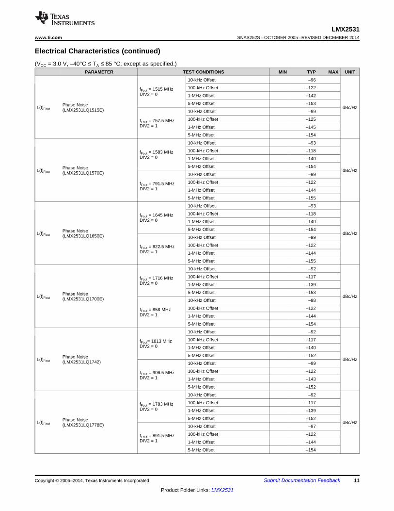
7.7 Typical Performance CharacteristicsSee Table 1.
Figure 1. OSCin Input Impedance
14 Submit Documentation Feedback Copyright © 2005–2014, Texas Instruments Incorporated
Product Folder Links: LMX2531

VCOVREG
ChargePump
FastLockI
RDivider
Serial InterfaceControl
DATA
CLK
LE
CE
PLL VREG1
VregVCO
VrefVCO
OSCin
OSCin*
Fout
Vtune
CPout
FLout
Ftest/ LD
DIGVREG
PLL VREG2
PrescalerN
Divider
CompMUX
1/2
LMX2531www.ti.com SNAS252S –OCTOBER 2005–REVISED DECEMBER 2014
8 Detailed Description
8.1 OverviewThe LMX2531 is a low-power, high-performance frequency synthesizer system which includes the PLL, VCO,and partially integrated loop filter. Feature Description gives a discussion of the various blocks of this device.
8.2 Functional Block Diagram
8.3 Feature Description
8.3.1 Reference Oscillator InputBecause the VCO frequency calibration algorithm is based on clocks from the OSCin pin, there are certain bitsthat need to be set depending on the OSCin frequency. XTLSEL (R6[22:20]) and XTLDIV (R7[9:8]) are bothneed to be set based on the OSCin frequency, fOSCin. For some options and for low OSCin frequencies, theXTLMAN (R7[21:10]) and XTLMAN2 (R8[4]) words need to be set to the correct value.
Table 1. OSCin Input Impedance (See Figure 1)FREQUENCY POWERED UP (kΩ) POWERED DOWN (kΩ)
(MHz) REAL IMAGINARY MAGNITUDE REAL IMAGINARY MAGNITUDE1 4.98 –2.70 5.66 6.77 –8.14 10.595 3.44 –3.04 4.63 5.73 –6.72 9.0310 1.42 –2.67 3.02 1.72 –5.24 5.5120 0.52 –1.63 1.71 0.53 –2.94 2.9830 0.29 –1.22 1.25 0.26 –2.12 2.1440 0.18 –0.92 0.94 0.17 –1.58 1.5950 0.13 –0.74 0.75 0.14 –1.24 1.2560 0.10 –0.63 0.64 0.10 –1.06 1.0670 0.09 –0.56 0.56 0.09 –0.95 0.9580 0.07 –0.50 0.50 0.08 –0.86 0.8790 0.07 –0.46 0.46 0.07 –0.80 0.80
Copyright © 2005–2014, Texas Instruments Incorporated Submit Documentation Feedback 15
Product Folder Links: LMX2531
LMX2531SNAS252S –OCTOBER 2005–REVISED DECEMBER 2014 www.ti.com
Feature Description (continued)Table 1. OSCin Input Impedance (See Figure 1) (continued)
FREQUENCY POWERED UP (kΩ) POWERED DOWN (kΩ)(MHz) REAL IMAGINARY MAGNITUDE REAL IMAGINARY MAGNITUDE100 0.06 –0.41 0.42 0.07 –0.72 0.72110 0.06 –0.37 0.38 0.07 –0.65 0.65120 0.05 –0.34 0.34 0.06 –0.59 0.59130 0.05 –0.32 0.32 0.06 –0.55 0.55140 0.04 –0.29 0.30 0.05 –0.50 0.50150 0.04 –0.27 0.28 0.05 –0.47 0.47
8.3.2 R DividerThe R divider divides the OSCin frequency down to the phase detector frequency. The R divider value, R, isrestricted to the values of 1, 2, 4, 8, 16, and 32. If R is greater than 8, then this also puts restrictions on thefractional denominator, FDEN, than can be used. This is discussed in greater depth in later sections.
8.3.3 Phase Detector and Charge PumpThe phase detector compares the outputs of the R and N dividers and puts out a correction currentcorresponding to the phase error. The phase detector frequency, fPD, can be calculated as shown in Equation 1.
fPD = fOSCin / R (1)
Choosing R = 1 yields the highest possible phase detector frequency and is optimum for phase noise, althoughthere are restrictions on the maximum phase detector frequency which could force the R value to be larger. Thefar out PLL noise improves 3 dB for every doubling of the phase detector frequency, but at lower offsets, thiseffect is much less due to the PLL 1 / f noise. Aside from getting the best PLL phase noise, higher phasedetector frequencies also make it easier to filter the noise that the delta-sigma modulator produces, which peaksat an offset frequency of fPD / 2 from the carrier. The LMX2531 also has 16 levels of charge pump currents and ahighly flexible fractional modulus. Increasing the charge pump current improves the phase noise about 3 dB perdoubling of the charge pump current, although there are small diminishing returns as the charge pump currentincreases.
From a loop filter design and PLL phase noise perspective, one might think to always design with the highestpossible phase detector frequency and charge pump current. However, if one considers the worst case fractionalspurs that occur at an output frequency equal to 1 channel spacing away from a multiple of the fOSCin, then thisgives reason to reconsider. If the phase detector frequency or charge pump currents are too high, then thesespurs could be degraded, and the loop filter may not be able to filter these spurs as well as theoreticallypredicted. For optimal spur performance, a phase detector frequency around 2.5 MHz and a charge pumpcurrent of 1X are recommended.
8.3.4 N Divider and Fractional CircuitryThe N divider in the LMX2531 includes fractional compensation and can achieve any fractional denominatorbetween 1 and 4,194,303. The integer portion, NInteger, is the whole part of the N divider value and the fractionalportion, NFractional, is the remaining fraction. So in general, the total N divider value, N, is determined byEquation 2.
N = NInteger + NFractional (2)
For example, if the phase detector frequency (fPD) was 10 MHz and the VCO frequency (fVCO) was 1736.1 MHz,then N would be 173.61. This would imply that NInteger is 173 and NFractional is 61/100. NInteger has some minimumvalue restrictions that are arise due to the architecture of this divider. The first restrictions arise because the Ndivider value is actually formed by a quadruple modulus 16/17/20/21 prescaler, which creates minimum dividevalues. NInteger is further restricted because the LMX2531 due to the fractional engine of the N divider.
16 Submit Documentation Feedback Copyright © 2005–2014, Texas Instruments Incorporated
Product Folder Links: LMX2531

LMX2531www.ti.com SNAS252S –OCTOBER 2005–REVISED DECEMBER 2014
The fractional word, NFractional , is a fraction formed with the NUM and DEN words. In the example used here withthe fraction of 61/100, NUM = 61 and DEN = 100. The fractional denominator value, DEN, can be set from 2 to4,194,303. The case of DEN = 0 makes no sense, because this would cause an infinite N value; the case of 1makes no sense either (but could be done), because integer mode should be used in these applications. Allother values in this range, like 10, 32, 42, 734, or 4,000,000 are all valid. Once the fractional denominator, DEN,is determined, the fractional numerator, NUM, is intended to be varied from 0 to DEN-1.
In general, the fractional denominator, DEN, can be calculated by dividing the phase detector frequency by thegreatest common divisor (GCD) of the channel spacing (fCH) and the phase detector frequency. If the channelspacing is not obvious, then it can be calculated as the greatest common divisor of all the desired VCOfrequencies.
FDEN = k × fPD / GCD (fPD , fCH) k = 1, 2, 3 .. (3)
For example, consider the case of a 10 MHz phase detector frequency and a 200 kHz channel spacing at theVCO output. The greatest common divisor of 10 MHz and 200 kHz is just 200 kHz. If one takes 10 MHz dividedby 200 kHz, the result is 50. So a fractional denominator of 50, or any multiple of 50 would work in this example.Now consider a case with a 10 MHz phase detector frequency and a 30 kHz channel spacing. The greatestcommon divisor of 10 MHz and 30 kHz is 10 kHz. The fractional denominator therefore must be a multiple 1000,because this is 10 MHz divided by 10 kHz. For a final example, consider an application with a fixed outputfrequency of 2110.8 MHz and a OSCin frequency of 19.68 MHz. If the phase detector frequency is chosen to be19.68 MHz, then the channel spacing can be calculated as the greatest common multiple of 19.68 MHz and2110.8 MHz, which is 240 kHz. The fractional denominator is therefore a multiple of 41, which is 19.68 MHz /240 kHz. Refer to AN-1865 Frequency Synthesis and Planning for PLL Architectures (SNAA061) for more detailson frequency planning.
To achieve a fractional N value, an integer N divider is modulated between different values. This gives rise tothree main degrees of freedom with the LMX2531 delta-sigma engine including the modulator order, dithering,and the way that the fractional portion is expressed. The first degree of freedom is the modulator order, whichgives the user the ability to optimize for a particular application. The modulator order can be selected as zero(integer mode), two, three, or four. One simple technique to better understand the impact of the delta-sigmafractional engine on noise and spurs is to tune the VCO to an integer channel and observe the impact ofchanging the modulator order from integer mode to a higher order. The higher the fractional modulator order is,the lower the spurs theoretically are. However, this is not always the case, and the higher order fractionalmodulator can sometimes give rise to additional spurious tones, but this is dependent on the application. Thesecond degree of freedom with the LMX2531 delta-sigma engine is dithering. Dithering is often effective inreducing these additional spurious tones, but can add phase noise in some situations. The third degree offreedom is the way that the fraction is expressed. For example, 1/10 can be expressed as 100000/1000000.Expressing the fraction in higher order terms sometimes improves the performance, particularly when dithering isused. In conclusion, there are some guidelines to getting the optimum choice of settings, but these optimumsettings are application specific. Refer to AN-1879 Fractional N Frequency Synthesis (SNAA062) for a muchmore detailed discussion on fractional PLLs and fractional spurs.
8.3.5 Partially Integrated Loop FilterThe LMX2531 integrates the third pole (formed by R3 and C3) and fourth pole (formed by R4 and C4) of the loopfilter. The values for C3, C4, R3, and R4 can also be programmed independently through the MICROWIREinterface and also R3 and R4 can be changed during FastLock, for minimum lock time. The larger the values ofthese components, the stronger the attenuation of the internal loop filter. The maximum attenuation can beachieved by setting R3 = R4 = 40 kΩ and C3 = C4 = 100 pF while the minimum attenuation is achieved bydisabling the loop filter by setting EN_LPFLTR (R6[15]) to zero. Note that when the internal loop filter is disabled,there is still a small amount of input capacitance on front of the VCO on the order of 200 pF.
Because that the internal loop filter is on-chip, it is more effective at reducing certain spurs than the external loopfilter. The higher order poles formed by the integrated loop filter are also helpful for attenuating noise due to thedelta-sigma modulator. This noise produced by the delta-sigma modulator is outside the loop bandwidth anddependent on the modulator order. Although setting the filtering for maximum attenuation gives the best filtering,it puts increased restrictions on how wide the loop bandwidth of the system can be, which corresponds to thecase where the shunt loop filter capacitor, C1, is zero. Increasing the charge pump current and/or the phasedetector frequency increases the maximum attainable loop bandwidth when designing with the integrated filter. It
Copyright © 2005–2014, Texas Instruments Incorporated Submit Documentation Feedback 17
Product Folder Links: LMX2531
LMX2531SNAS252S –OCTOBER 2005–REVISED DECEMBER 2014 www.ti.com
is recommended to set the internal loop filter as high as possible without restricting the loop bandwidth of thesystem more than desired. If some setting between the minimum and maximum value is desired, it is preferableto reduce the resistor values before reducing the capacitor values because this will reduce the thermal noisecontribution of the loop filter resistors. For design tools and more information on partially integrated loop filters,go to the Clock Design Tool on www.ti.com.
8.3.6 Low Noise, Fully Integrated VCOThe LMX2531 includes a fully integrated VCO, including the inductors. For optimum phase noise performance,this VCO has frequency and phase noise calibration algorithms. The frequency calibration algorithm is necessarybecause the VCO internally divides up the frequency range into several bands, to achieve a lower tuning gain,and therefore better phase noise performance. The frequency calibration routine is activated any time that the R0register is programmed. There are several bits including LOCKMODE and XTLSEL that need to be set properlyfor this calibration to be performed in a reliable fashion. If the temperature shifts considerably and the R0 registeris not programmed, then it cannot drift more than the maximum allowable drift for continuous lock, ΔTCL, or elsethe VCO is not ensured to stay in lock. The phase noise calibration algorithm is necessary to achieve the lowestpossible phase noise. Each version of the LMX2531, the VCO_ACI_SEL bit (R6[19:16]) needs to be set to thecorrect value to ensure the best possible phase noise.
The gain of the VCO can change considerably over frequency. It is lowest at the minimum frequency and highestat the maximum frequency. This range is specified in Electrical Characteristics of the data sheet. When designingthe loop filter, the following method is recommended to determine what VCO gain to design to. First, take thegeometric mean of the minimum and maximum frequencies that are to be used. Then use a linear approximationto extrapolate the VCO gain. Suppose the application requires the LMX2531LQ2080E PLL to tune from 2100 to2150 MHz. The geometric mean of these frequencies is sqrt (2100 × 2150) MHz = 2125 MHz. The VCO gain isspecified as 9 MHz/V at 1904 MHz and 20 MHz/V at 2274 MHz. Over this range of 370 MHz, the VCO gainchanges 11 MHz/V. Therefore, at 2125 MHz, the VCO gain would be approximately 9 + (2125 – 1904) × 11 / 370= 15.6 MHz/V. Although the VCO gain can change from part to part, this variation is small compared to howmuch the VCO gain can change over frequency.
The VCO frequency is related to the other frequencies and divider values as shown in Equation 4.fVCO = fPD × N = fOSCin × N / R (4)
8.3.7 Programmable VCO DividerAll options of the LMX2531 offer the option of dividing the VCO output by two to get half of the VCO frequency atthe Fout pin. The channel spacing at the Fout pin is also divided by two as well. Because this divide by two isoutside feedback path between the VCO and the PLL, enabling does require one to change the N divider, Rdivider, or loop filter values. When this divider is enabled, there will be some far-out phase noise contribution tothe VCO noise. Note that the R0 register should be reprogrammed the first time after the DIV2 bit is enabled ordisabled for optimal phase noise performance. The frequency at the Fout pin is related to the VCO frequencyand divider value, D, as shown in Equation 5.
fFout = fVCO / D (5)
18 Submit Documentation Feedback Copyright © 2005–2014, Texas Instruments Incorporated
Product Folder Links: LMX2531
tCEStCS
D19 D18 D17 D16
tCHtCWH
tCWL
D15 D0 C3 C2 C1 C0
MSB LSB
DATA
CLK
LE
tES
tEWH
LMX2531www.ti.com SNAS252S –OCTOBER 2005–REVISED DECEMBER 2014
8.3.8 Serial Data Timing RequirementsSee MICROWIRE Timing Requirements.
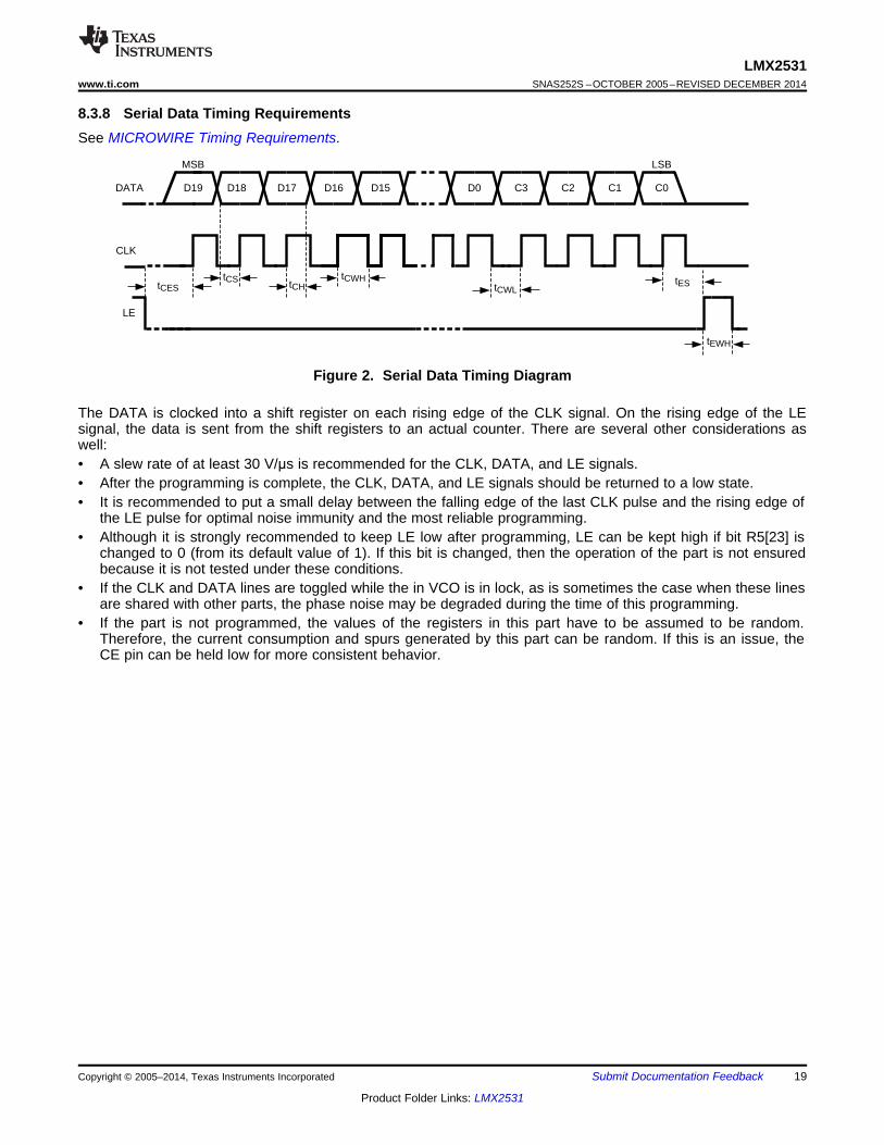
Figure 2. Serial Data Timing Diagram
The DATA is clocked into a shift register on each rising edge of the CLK signal. On the rising edge of the LEsignal, the data is sent from the shift registers to an actual counter. There are several other considerations aswell:• A slew rate of at least 30 V/μs is recommended for the CLK, DATA, and LE signals.• After the programming is complete, the CLK, DATA, and LE signals should be returned to a low state.• It is recommended to put a small delay between the falling edge of the last CLK pulse and the rising edge of
the LE pulse for optimal noise immunity and the most reliable programming.• Although it is strongly recommended to keep LE low after programming, LE can be kept high if bit R5[23] is
changed to 0 (from its default value of 1). If this bit is changed, then the operation of the part is not ensuredbecause it is not tested under these conditions.
• If the CLK and DATA lines are toggled while the in VCO is in lock, as is sometimes the case when these linesare shared with other parts, the phase noise may be degraded during the time of this programming.
• If the part is not programmed, the values of the registers in this part have to be assumed to be random.Therefore, the current consumption and spurs generated by this part can be random. If this is an issue, theCE pin can be held low for more consistent behavior.
Copyright © 2005–2014, Texas Instruments Incorporated Submit Documentation Feedback 19
Product Folder Links: LMX2531

LMX2531SNAS252S –OCTOBER 2005–REVISED DECEMBER 2014 www.ti.com
8.4 Device Functional ModesThe LMX2531 operates mainly in the active mode. The other two modes are reset and powerdown modes. Thepowerdown mode can be achieved by taking the CE pin to 0 V. The reset mode is achieved if the REG_RST bitis set to 1.
8.5 ProgrammingThe LMX2531 is programmed using 11 24-bit registers used to control the LMX2531 operation. A 24-bit shiftregister is used as a temporary register to indirectly program the on-chip registers. The shift register consists of adata field and an address field. The last 4 register bits, CTRL[3:0] form the address field, which is used todecode the internal register address. The remaining 20 bits form the data field DATA[19:0]. While LE is low,serial data is clocked into the shift register upon the rising edge of clock (data is programmed MSB first). WhenLE goes high, data is transferred from the data field into the selected register bank. Although there are actually14 registers in this part, only a portion of them should be programmed, because the state of the other hiddenregisters (R13, R11, and R10) are set during the initialization sequence. Although it is possible to program thesehidden registers, as well as a lot of bits that are defined to either 1 or 0, the user should not experiment withthese hidden registers and bits, because the parts are not tested under these conditions and doing so will mostlikely degrade performance.
Table 2. Register Location Truth TableC3 C2 C1 C0 Data Address1 1 0 0 R121 0 0 1 R91 0 0 0 R80 1 1 1 R70 1 1 0 R60 1 0 1 R50 1 0 0 R40 0 1 1 R30 0 1 0 R20 0 0 1 R10 0 0 0 R0
20 Submit Documentation Feedback Copyright © 2005–2014, Texas Instruments Incorporated
Product Folder Links: LMX2531

LMX2531www.ti.com SNAS252S –OCTOBER 2005–REVISED DECEMBER 2014
8.6 Register Maps
8.6.1 General Programming Information
Table 3. Programming Register StructureDATA[19:0] CONTROL[3:0]
MSB LSBD19 D18 D17 D16 D15 D14 D13 D12 D11 D10 D D D D D D D D D D C C C C0
9 8 7 6 5 4 3 2 1 0 3 2 1
8.6.1.1 Initialization SequenceThe initial loading sequence from a cold start is described in Table 4. The registers must be programmed in ordershown. There must be a minimum of 10 ms between the time when R5 is last loaded and R1 is loaded to ensuretime for the LDOs to power up properly.
Table 4. Initialization SequenceREG. 23 22 21 20 19 18 17 16 15 14 13 12 11 10 9 8 7 6 5 4 3 2 1 0
DATA[19:0] C3 C2 C1 C0R5 1 0 0 0 0 1 0 0 0 0 0 0 0 0 0 0 0 0 0 0 0 1 0 1INIT1R5 1 0 0 0 0 0 0 0 0 0 0 0 0 0 0 0 0 0 0 0 0 1 0 1INIT2R5 1 0 0 0 0 0 0 0 0 0 0 0 0 1 1 1 1 1 1 1 0 1 0 1R12 Program R12 as shown in the complete register map. 1 1 0 0R9 Program R9 as shown in the complete register map. 1 0 0 1
See individual section for Register R8 programming information.R8 1 0 0 0Programming of this register is necessary under specific circumstances.R7 See individual section for Register R7 programming information. 0 1 1 1R6 See individual section for Register R6 programming information. 0 1 1 0
See individual section for Register R4 programming information.R4 0 1 0 0Register R4 only needs to be programmed if FastLock is used.R3 See individual section for Register R3 programming information. 0 0 1 1R2 See individual section for Register R2 programming information. 0 0 1 0R1 See individual section for Register R1 programming information. 0 0 0 1R0 See individual section for Register R0 programming information. 0 0 0 0
Copyright © 2005–2014, Texas Instruments Incorporated Submit Documentation Feedback 21
Product Folder Links: LMX2531

LMX2531SNAS252S –OCTOBER 2005–REVISED DECEMBER 2014 www.ti.com
8.6.1.2 Complete Register Content MapTable 5 shows all the programmable bits for the LMX2531. No programming order or initialization sequence is implied by Table 5, only the location of theprogramming information.
Table 5. Complete Register Content Map23 22 21 20 19 18 17 16 15 14 13 12 11 10 9 8 7 6 5 4 3 2 1 0
DATA[19:0] C3 C2 C1 C0
RE
GIS
TER
N NUMR0 0 0 0 0[7:0] [11:0]
ICP N NUMR1 0 0 1 0 0 0 1[3:0] [10:8] [21:12]
DEN RR2 0 1 0 0 1 0[11:0] [5:0]
DITHER ORDER FoLD DENR3 DIV2 FDM 0 0 1 1[1:0] [1:0] [3:0] [21:12]
ICPFL TOCR4 0 0 0 1 0 0[3:0] [13:0]
EN_ EN_REG EN_ EN_PLL PLL EN_ EN_ EN_R5 1 0 0 0 0 _RS 0 0 0 0 0 0 0 DIG VCO 0 1 0 1LDO LDO OSC VCO PLLT LDO LD2 1
EN_ R4_ADJ_F R3_ADJ_FXTLSEL VCO_ACI_SEL R4_ADJ R3_ADJ C3_4_ADJR6 0 LPF L L 0 1 1 0[2:0] [3:0] [1:0] [1:0] [2:0]LTR [1:0] [1:0]
XTLMAN XTLDIVR7 0 0 0 0 0 0 0 1 1 1[11:0] [1:0]
XTLLOCKR8 0 0 0 0 0 0 1 0 0 0 0 0 0 0 0 0 0 MAN 1 0 0 0MODE 2
R9 0 0 0 0 0 0 0 0 0 0 0 0 1 0 1 1 1 0 1 0 1 0 0 1
R12 0 0 0 0 0 0 0 1 0 0 0 0 0 1 0 0 1 0 0 0 1 1 0 0
22 Submit Documentation Feedback Copyright © 2005–2014, Texas Instruments Incorporated
Product Folder Links: LMX2531

LMX2531www.ti.com SNAS252S –OCTOBER 2005–REVISED DECEMBER 2014
8.6.1.3 Register R0
The action of programming the R0 register activates a frequency calibration routine for the VCO. This calibrationis necessary to get the VCO to center the tuning voltage for optimal performance. If the temperature driftsconsiderably, then the PLL should stay in lock, provided that the temperature drift specification is not violated.
8.6.1.3.1 NUM[10:0] and NUM[21:12] -- Fractional Numerator
The NUM word is split between the R0 register and R1 register. The Numerator bits determine the fractionalnumerator for the delta-sigma PLL. This value can go from 0 to 4095 when the FDM bit (R3[22]) is 0 (the otherbits in this register are ignored), or 0 to 4194303 when the FDM bit is 1.
Table 6. Fractional NumeratorFRACTIONAL NUM[21:12] NUM[11:0]NUMERATOR
0 0 0 0 0 0 0 0 0 0 0 0 0 0 0 0 0 0 0 0 0 0 0...
409503 1 1 1 1 1 1 1 1 1 1 1 1 1 1 1 1 1 1 1 1 1 14096 0 0 0 0 0 0 0 0 0 0 1 0 0 0 0 0 0 0 0 0 0 0
...4194303 1 1 1 1 1 1 1 1 1 1 1 1 1 1 1 1 1 1 1 1 1 1
Note that there are restrictions on the fractional numerator value depending on the R divider value if it is 16 or32.
8.6.1.3.2 N[7:0] and N[10:8]
The N counter is 11 bits. 8 of these bits are located in the R0 register, and the remaining 3 (MSB bits) arelocated in the R1 register. The LMX2531 consists of an A, B, and C counter, which work in conjunction with the16/17/20/21 prescaler to form the final N counter value.
Table 7. N Divider ValueN[10:8] N[7:0]
N Value C B A<48 Values less than 48 are prohibited.
48 - 51 Possible ONLY with ORDER = 1 (Reset Modulator)52-54 Values of 52 - 54 are prohibited.
55 0 0 0 0 0 1 1 0 1 1 1...
2039 1 1 1 1 1 1 1 0 1 1 1
8.6.1.4 Register R1
8.6.1.4.1 NUM[21:12]
These are the MSB bits in for the fractional numerator that already have been described.
8.6.1.4.2 N[10:8] -- 3 MSB Bits for the N Counter
These are the 2 MSB bits for the N counter, which were discussed in Register R0.
8.6.1.4.3 ICP[3:0] -- Charge Pump Current
This bit programs the charge pump current in from 90 µA to 1440 µA in 90 µA steps. In general, higher chargepump currents yield better phase noise for the PLL, but also can cause higher spurs.
Copyright © 2005–2014, Texas Instruments Incorporated Submit Documentation Feedback 23
Product Folder Links: LMX2531
LMX2531SNAS252S –OCTOBER 2005–REVISED DECEMBER 2014 www.ti.com
Table 8. Charge Pump CurrentTYPICAL CHARGE PUMP CURRENTICP CHARGE PUMP STATE at 3 VOLTS (µA)
0 1X 901 2X 1802 3X 2703 4X 3604 5X 4505 6X 5406 7X 6307 8X 7208 9X 8109 10X 90010 11X 99011 12X 108012 13X 117013 14X 126014 15X 135015 16X 1440
8.6.1.5 Register R2
8.6.1.5.1 R[5:0] -- R Counter Value
These bits determine the phase detector frequency. The OSCin frequency is divided by this R counter value.Note that only the values of 1, 2, 4, 8, 16, and 32 are allowed.
Table 9. R Divider ValueFRACTIONAL
R VALUE DENOMINATOR R[5:0]RESTRICTIONS
0,3,5-7,9-15,17-31, n/a These values are illegal.
33-631 none 0 0 0 0 0 12 none 0 0 0 0 1 04 none 0 0 0 1 0 08 none 0 0 1 0 0 0
Must be divisible16 0 1 0 0 0 0by 2Must be divisible32 1 0 0 0 0 0by 4
The R counter value can put some restrictions on the fractional denominator. In the case that it is 16, thefractional denominator must be divisible by 2, which is equivalent to saying that the LSB of the fractionaldenominator word is zero. In the case that the R counter is 32, the two LSB bits of the fractional denominatorword must also be zero, which is equivalent to saying that the fractional denominator must be divisible by 4.Because the fractional denominator can be very large, this should cause no issues. For instance, if one wantedto achieve a fractional word of 1/65, and the R counter value was 16, the fractional word could be changed to4/260, and the same resolution could be achieved.
24 Submit Documentation Feedback Copyright © 2005–2014, Texas Instruments Incorporated
Product Folder Links: LMX2531

LMX2531www.ti.com SNAS252S –OCTOBER 2005–REVISED DECEMBER 2014
8.6.1.5.2 DEN[21:12] and DEN[11:0]-- Fractional Denominator
These bits determine the fractional denominator. Note that the MSB bits for this word are in register R3. If theFDM bit is set to 0, DEN[21:12] are ignored. The fractional denominator should only be set to zero if thefractional circuitry is being disabled by setting ORDER = 1. A value of one never makes sense to use. All othervalues could reasonably be used in fractional mode.
Table 10. Fractional DenominatorFRACTIONAL DEN[21:12] DEN[11:0]DENOMINATOR
0 0 0 0 0 0 0 0 0 0 0 0 0 0 0 0 0 0 0 0 0 0 0...
4095 1 1 1 1 1 1 1 1 1 1 1 1 1 1 1 1 1 1 1 1 1 14096 0 0 0 0 0 0 0 0 0 1 0 0 0 0 0 0 0 0 0 0 0 0
...4194303 1 1 1 1 1 1 1 1 1 1 1 1 1 1 1 1 1 1 1 1 1 1
8.6.1.6 Register R3
8.6.1.6.1 DEN[21:12] -- Extension for the Fractional Denominator
These are the MSB bits of the DEN word, which have already been discussed.
8.6.1.6.2 FoLD[3:0] -- Multiplexed Output for Ftest/LD Pin
The FoLD[3:0] word is used to program the output of the Ftest/LD pin. This pin can be used for a generalpurpose I/O pin, a lock detect pin, and for diagnostic purposes. When programmed to the digital lock detectstate, the output of the Ftest/LD pin will be high when the part is in lock, and low otherwise. Lock is determinedby comparing the input phases to the phase detector. The analog lock detect modes put out a high signal withvery fast negative pulses, that correspond to when the charge pump comes on. This output can be low passfiltered with an RC filter to determine the lock detect state. If the open drain state is used, a additional pullupresistor is required. For diagnostic purposes, the options that allow one to view the output of the R counter or theN counter can be very useful. Be aware that the output voltage level of the Ftest/LD is not equal to the supplyvoltage of the part, but rather is given by VOH and VOL in Electrical Characteristics.
Table 11. Ftest/LD Pin FunctionsFoLD OUTPUT TYPE FUNCTION
0 High Impedance Disabled1 Push-Pull Logical High State2 Push-Pull Logical Low State3 Push-Pull Digital Lock Detect4 N/A Reserved5 Push-Pull N Counter Output Divided by 26 Open-Drain Analog Lock Detect7 Push-Pull Analog Lock Detect8 N/A Reserved9 N/A Reserved10 N/A Reserved11 N/A Reserved12 N/A Reserved13 N/A Reserved14 Push-Pull R Counter Output15 N/A Reserved
Copyright © 2005–2014, Texas Instruments Incorporated Submit Documentation Feedback 25
Product Folder Links: LMX2531
LMX2531SNAS252S –OCTOBER 2005–REVISED DECEMBER 2014 www.ti.com
8.6.1.6.3 ORDER -- Order of Delta-Sigma Modulator
This bit determines the order of the delta-sigma modulator in the PLL. In general, higher order fractionalmodulators tend to reduce the primary fractional spurs that occur at increments of the channel spacing, but canalso create spurs that are at a fraction of the channel spacing, if there is not sufficient filtering. The optimalchoice of modulator order is very application specific, however, a third order modulator is a good starting point ifnot sure what to try first.
Table 12. Delta-Sigma ModulatorORDER DELTA-SIGMA MODULATOR ORDER
0 FourthReset Modulator1 (Integer Mode - all fractions are ignored)
2 Second3 Third
8.6.1.6.4 DITHER -- Dithering
Dithering is useful in reducing fractional spurs, especially those that occur at a fraction of the channel spacing.The only exception is when the fractional numerator is zero. In this case, dithering usually is not a benefit.Dithering also can sometimes increase the PLL phase noise by a fraction of a dB. In general, if dithering isdisabled, phase noise may be slightly better inside the loop bandwidth of the system, but spurs are likely to beworse too.
Table 13. Fractional DitheringDITHER DITHERING MODE
0 Weak Dithering1 Reserved2 Strong Dithering3 Dithering Disabled
8.6.1.6.5 FDM -- Fractional Denominator Mode
When this bit is set to 1, the 10 MSB bits for the fractional numerator and denominator are considered. Thisallows the fractional denominator to range from 1 to 4,194,303. If this bit is set to zero, only the 12 LSB bits ofthe fractional numerator and denominator are considered, and this allows a fractional denominator from 1 to4095. When this bit is disabled, the current consumption is about 0.5 mA lower.
8.6.1.6.6 DIV2
When this bit is enabled, the output of the VCO is divided by 2. Enabling this bit does have some impact onharmonic content and output power.
Table 14. VCO Output DividerDIV2 VCO OUTPUT FREQUENCY
0 Not Divided by 21 Divided by 2
8.6.1.7 Register R4
8.6.1.7.1 TOC[13:0] -- Time-Out Counter for FastLock
When the value of this word is 3 or less, then FastLock is disabled, and this pin can only be used for generalpurpose I/O. When this value is 4 or greater, the time-out counter is engaged for the amount of phase detectorcycles shown in Table 15.
26 Submit Documentation Feedback Copyright © 2005–2014, Texas Instruments Incorporated
Product Folder Links: LMX2531
LMX2531www.ti.com SNAS252S –OCTOBER 2005–REVISED DECEMBER 2014
Table 15. FastLock Timeout CounterTOC VALUE FLout PIN STATE TIMEOUT COUNT
0 High Impedance 01 Low Always Enabled2 Low 03 High 04 Low 4 × 2 Phase Detector. . .
16383 Low 16383 × 2 Phase Detector
When this count is active, the FLout pin is grounded, the FastLock current is engaged, and the resistors R3 andR4 are also potentially changed. The table below summarizes the bits that control various values in and out ofFastLock differences.
Table 16. FastLock Filter ValuesCHARGE PUMPFastLock STATE FLout R3 R4CURRENT
Steady State High Impedance ICP R3_ADJ R4_ADJFastlock Grounded ICPFL R3_ADJ_FL R4_ADJ_FL
8.6.1.7.2 ICPFL[3:0] -- Charge Pump Current for Fastlock
When FastLock is enabled, this is the charge pump current that is used for faster lock time.
Table 17. FastLock Charge Pump CurrentTYPICAL Fastlock CHARGE PUMPICPFL Fastlock CHARGE PUMP STATE CURRENT at 3 VOLTS (µA)
0 1X 901 2X 1802 3X 2703 4X 3604 5X 4505 6X 5406 7X 6307 8X 7208 9X 8109 10X 90010 11X 99011 12X 108012 13X 117013 14X 126014 15X 135015 16X 1440
8.6.1.8 Register R5
8.6.1.8.1 EN_PLL -- Enable Bit for PLL
When this bit is set to 1 (default), the PLL is powered up, otherwise, it is powered down.
8.6.1.8.2 EN_VCO -- Enable Bit for the VCO
When this bit is set to 1 (default), the VCO is powered up, otherwise, it is powered down.
Copyright © 2005–2014, Texas Instruments Incorporated Submit Documentation Feedback 27
Product Folder Links: LMX2531
LMX2531SNAS252S –OCTOBER 2005–REVISED DECEMBER 2014 www.ti.com
8.6.1.8.3 EN_OSC -- Enable Bit for the Oscillator Inverter
When this bit is set to 1 (default), the reference oscillator is powered up, otherwise it is powered down.
8.6.1.8.4 EN_VCOLDO -- Enable Bit for the VCO LDO
When this bit is set to 1 (default), the VCO LDO is powered up, otherwise it is powered down.
8.6.1.8.5 EN_PLLLDO1 -- Enable Bit for the PLL LDO 1
When this bit is set to 1 (default), the PLL LDO 1 is powered up, otherwise it is powered down.
8.6.1.8.6 EN_PLLLDO2 -- Enable Bit for the PLL LDO 2
When this bit is set to 1 (default), the PLL LDO 2 is powered up, otherwise it is powered down.
8.6.1.8.7 EN_DIGLDO -- Enable Bit for the digital LDO
When this bit is set to 1 (default), the Digital LDO is powered up, otherwise it is powered down.
8.6.1.8.8 REG_RST -- Resets All Registers to Default Settings
This bit needs to be programmed three times to initialize the part. When this bit is set to one, all registers are setto default mode, and the part is powered down. The second time the R5 register is programmed with REG_RST= 0, the register reset is released and the default states are still in the registers. However, because the defaultstates for the blocks and LDOs is powered off, it is therefore necessary to program R5 a third time so that all theLDOs and blocks can be programmed to a power up state. When this bit is set to 1, all registers are set to thedefault modes, but part is powered down. For normal operation, this bit is set to 0. Once this initialization is done,it is not necessary to do this again unless power is removed from the device.
8.6.1.9 Register R6
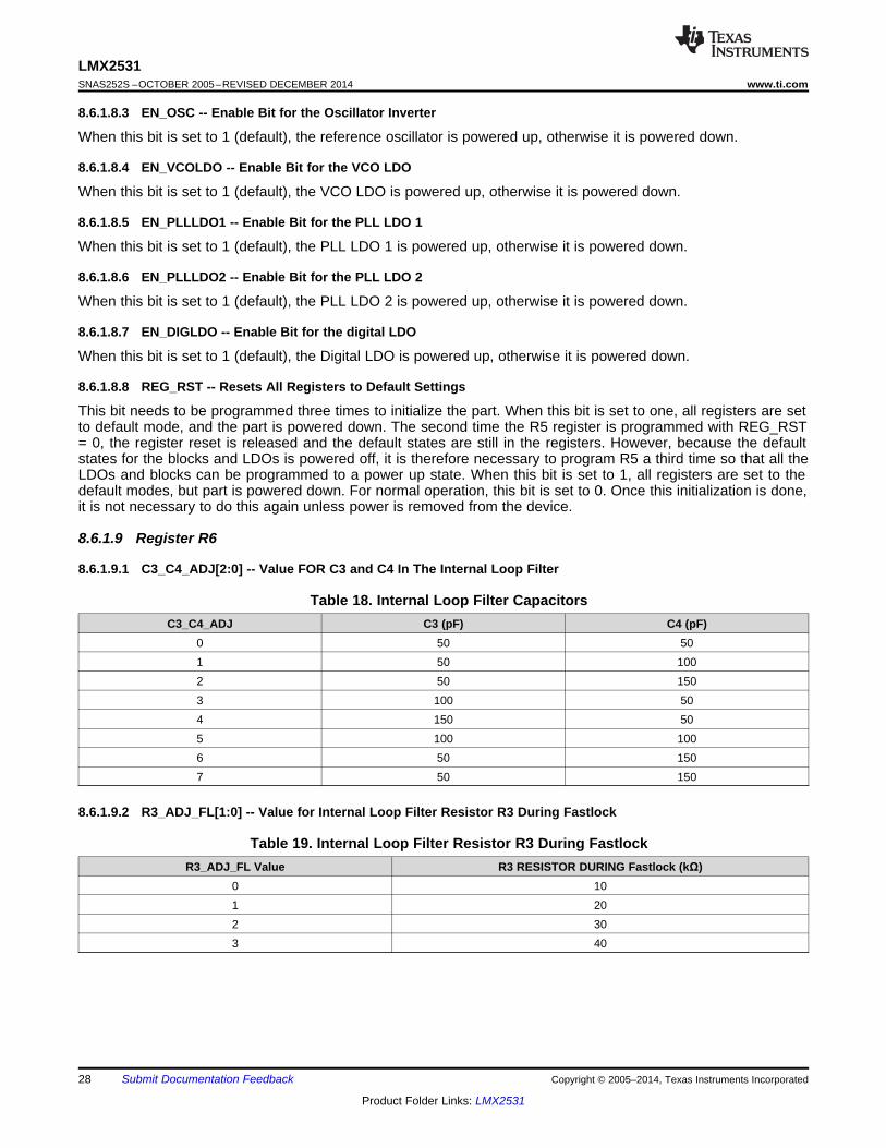
8.6.1.9.1 C3_C4_ADJ[2:0] -- Value FOR C3 and C4 In The Internal Loop Filter
Table 18. Internal Loop Filter CapacitorsC3_C4_ADJ C3 (pF) C4 (pF)
0 50 501 50 1002 50 1503 100 504 150 505 100 1006 50 1507 50 150
8.6.1.9.2 R3_ADJ_FL[1:0] -- Value for Internal Loop Filter Resistor R3 During Fastlock
Table 19. Internal Loop Filter Resistor R3 During FastlockR3_ADJ_FL Value R3 RESISTOR DURING Fastlock (kΩ)
0 101 202 303 40
28 Submit Documentation Feedback Copyright © 2005–2014, Texas Instruments Incorporated
Product Folder Links: LMX2531
LMX2531www.ti.com SNAS252S –OCTOBER 2005–REVISED DECEMBER 2014
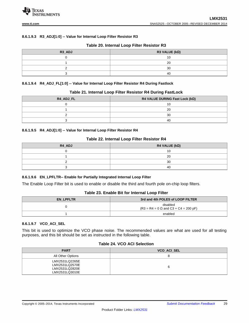
8.6.1.9.3 R3_ADJ[1:0] -- Value for Internal Loop Filter Resistor R3
Table 20. Internal Loop Filter Resistor R3R3_ADJ R3 VALUE (kΩ)
0 101 202 303 40
8.6.1.9.4 R4_ADJ_FL[1:0] -- Value for Internal Loop Filter Resistor R4 During Fastlock
Table 21. Internal Loop Filter Resistor R4 During FastLockR4_ADJ_FL R4 VALUE DURING Fast Lock (kΩ)
0 101 202 303 40
8.6.1.9.5 R4_ADJ[1:0] -- Value for Internal Loop Filter Resistor R4
Table 22. Internal Loop Filter Resistor R4R4_ADJ R4 VALUE (kΩ)
0 101 202 303 40
8.6.1.9.6 EN_LPFLTR-- Enable for Partially Integrated Internal Loop Filter
The Enable Loop Filter bit is used to enable or disable the third and fourth pole on-chip loop filters.
Table 23. Enable Bit for Internal Loop FilterEN_LPFLTR 3rd and 4th POLES of LOOP FILTER
disabled0 (R3 = R4 = 0 Ω and C3 + C4 = 200 pF)1 enabled
8.6.1.9.7 VCO_ACI_SEL
This bit is used to optimize the VCO phase noise. The recommended values are what are used for all testingpurposes, and this bit should be set as instructed in the following table.
Table 24. VCO ACI SelectionPART VCO_ACI_SEL
All Other Options 8LMX2531LQ2265ELMX2531LQ2570E 6LMX2531LQ2820ELMX2531LQ3010E
Copyright © 2005–2014, Texas Instruments Incorporated Submit Documentation Feedback 29
Product Folder Links: LMX2531
LMX2531SNAS252S –OCTOBER 2005–REVISED DECEMBER 2014 www.ti.com
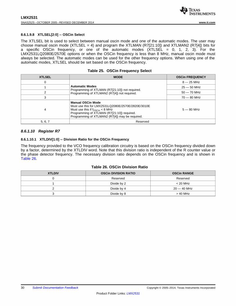
8.6.1.9.8 XTLSEL[2:0] -- OSCin Select
The XTLSEL bit is used to select between manual oscin mode and one of the automatic modes. The user maychoose manual oscin mode (XTLSEL = 4) and program the XTLMAN (R7[21:10]) and XTLMAN2 (R7[4]) bits fora specific OSCin frequency, or one of the automatic modes (XTLSEL = 0, 1, 2, 3). For theLMX2531LQ2080E/2570E options or when the OSCin frequency is less than 8 MHz, manual oscin mode mustalways be selected. The automatic modes can be used for the other frequency options. When using one of theautomatic modes, XTLSEL should be set based on the OSCin frequency.
Table 25. OSCin Frequency SelectXTLSEL MODE OSCin FREQUENCY
0 8 — 25 MHzAutomatic Modes1 25 — 50 MHzProgramming of XTLMAN (R7[21:10]) not required.
2 50 — 70 MHzProgramming of XTLMAN2 (R7[4]) not required.3 70 — 80 MHz
Manual OSCin ModeMust use this for LMX2531LQ2080E/2570E/2820E/3010E
4 Must use this if fOSCin < 8 MHz 5 — 80 MHzProgramming of XTLMAN (R7[21:10]) required.Programming of XTLMAN2 (R7[4]) may be required.
5, 6, 7 Reserved
8.6.1.10 Register R7
8.6.1.10.1 XTLDIV[1:0] -- Division Ratio for the OSCin Frequency
The frequency provided to the VCO frequency calibration circuitry is based on the OSCin frequency divided downby a factor, determined by the XTLDIV word. Note that this division ratio is independent of the R counter value orthe phase detector frequency. The necessary division ratio depends on the OSCin frequency and is shown inTable 26.
Table 26. OSCin Division RatioXTLDIV OSCin DIVISION RATIO OSCin RANGE
0 Reserved Reserved1 Divide by 2 < 20 MHz2 Divide by 4 20 — 40 MHz3 Divide by 8 > 40 MHz
30 Submit Documentation Feedback Copyright © 2005–2014, Texas Instruments Incorporated
Product Folder Links: LMX2531

LMX2531www.ti.com SNAS252S –OCTOBER 2005–REVISED DECEMBER 2014
8.6.1.10.2 XTLMAN[11:0] -- Manual OSCin Mode
XTLMAN must be programmed if word XTLSEL (XTLSEL[2:0] -- OSCin Select) is set to manual OSCin mode. Inthe table below, the proper value for XTLMAN is shown based on some common OSCin frequencies (fOSCin) andvarious LMX2531 options. For any OSCin frequency XTLMAN can be calculated as 16 × fOSCin / Kbit. fOSCin isexpressed in MHz and Kbit values for the LMX2531 frequency options can be found in Table 28.
Table 27. XTLMAN Values for Common OSCin FrequenciesfOSCinDEVICE
5 MHz 10 MHz 20 MHz 30.72 MHz 61.44 MHz 76.8 MHzLMX2531LQ1146E 53 107 213 327 655 819LMX2531LQ1226E 53 107 213 327 655 819LMX2531LQ1312E 47 94 188 289 578 722LMX2531LQ1415E 47 94 188 289 578 722LMX2531LQ1500E 40 80 160 246 492 614LMX1531LQ1515E 40 80 160 246 492 614LMX2531LQ1570E 38 76 152 234 468 585LMX2531LQ1650E 38 76 152 234 468 585LMX2531LQ1700E 35 70 139 214 427 534LMX2531LQ1742 32 64 128 197 393 492
LMX2531LQ1778E 31 62 123 189 378 473LMX2531LQ1910E 27 53 107 164 328 410LMX2531LQ2265E 20 40 80 123 246 307LMX2531LQ2080E 18 36 71 109 218 273LMX2531LQ2570E 13 27 53 82 164 205LMX2531LQ2820E 11 23 46 70 140 178LMX2531LQ3010E 10 20 40 61 123 154
Table 28. Kbit Values for Various LMX2531 OptionsDEVICE Kbit
LMX2531LQ1146E 1.5LMX2531LQ1226E 1.5LMX2531LQ1312E 1.7LMX2531LQ1415E 1.7LMX2531LQ1500E 2LMX2531LQ1515E 2LMX2531LQ1570E 2.1LMX2531LQ1650E 2.1LMX2531LQ1700E 2.3
LMX25311742 2.5LMX2531LQ1778E 2.6LMX2531LQ1910E 3LMX2531LQ2265E 4LMX2531LQ2080E 4.5LMX2531LQ2570E 6LMX2531LQ2820E 7LMX2531LQ3010E 8
Copyright © 2005–2014, Texas Instruments Incorporated Submit Documentation Feedback 31
Product Folder Links: LMX2531
LMX2531SNAS252S –OCTOBER 2005–REVISED DECEMBER 2014 www.ti.com
8.6.1.11 Register R8
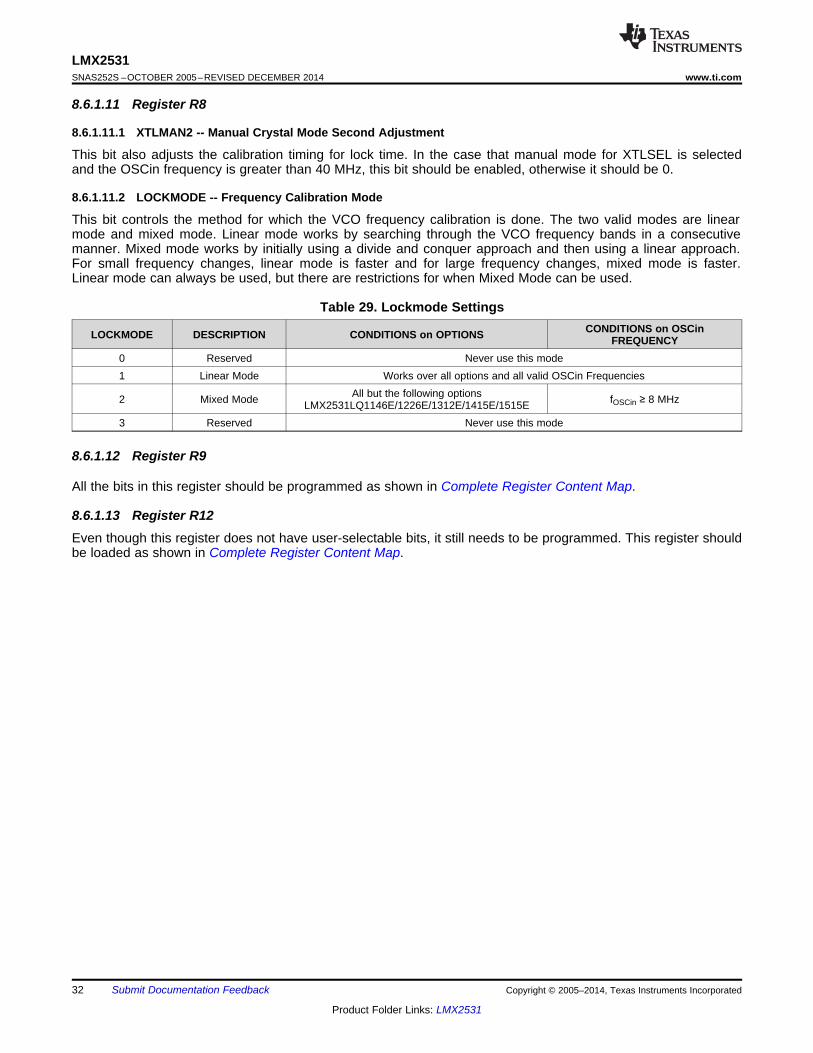
8.6.1.11.1 XTLMAN2 -- Manual Crystal Mode Second Adjustment
This bit also adjusts the calibration timing for lock time. In the case that manual mode for XTLSEL is selectedand the OSCin frequency is greater than 40 MHz, this bit should be enabled, otherwise it should be 0.
8.6.1.11.2 LOCKMODE -- Frequency Calibration Mode
This bit controls the method for which the VCO frequency calibration is done. The two valid modes are linearmode and mixed mode. Linear mode works by searching through the VCO frequency bands in a consecutivemanner. Mixed mode works by initially using a divide and conquer approach and then using a linear approach.For small frequency changes, linear mode is faster and for large frequency changes, mixed mode is faster.Linear mode can always be used, but there are restrictions for when Mixed Mode can be used.
Table 29. Lockmode SettingsCONDITIONS on OSCinLOCKMODE DESCRIPTION CONDITIONS on OPTIONS FREQUENCY
0 Reserved Never use this mode1 Linear Mode Works over all options and all valid OSCin Frequencies
All but the following options2 Mixed Mode fOSCin ≥ 8 MHzLMX2531LQ1146E/1226E/1312E/1415E/1515E3 Reserved Never use this mode
8.6.1.12 Register R9
All the bits in this register should be programmed as shown in Complete Register Content Map.
8.6.1.13 Register R12Even though this register does not have user-selectable bits, it still needs to be programmed. This register shouldbe loaded as shown in Complete Register Content Map.
32 Submit Documentation Feedback Copyright © 2005–2014, Texas Instruments Incorporated
Product Folder Links: LMX2531

DA
TA
CLK
LE CE
VregVCO
VrefVCO
OS
Cin
OS
Cin
*F
out
Vtu
ne
CP
out
FLo
utF
test
/LD
LMX2531
Microcontroller
VregBUF
VregPLL1
VregPLL2
VregDIG
VccVCO
VccBUF
VccPLL
VccDIG
1 PF
10:
10:
10:
10:
100 pF
10 PF
3.3: 4.7 PF
10 nF
100 nF
100 nF
TCXO
C1_LF
R2pLFR2_LF
C2_LF
1 PF
1 PF
1 PFPowerSupply
Tes
t
10 nF
10 nF
0.22: 470 nF
0.22: 470 nF
Circuit
LMX2531www.ti.com SNAS252S –OCTOBER 2005–REVISED DECEMBER 2014
9 Application and Implementation
NOTEInformation in the following applications sections is not part of the TI componentspecification, and TI does not warrant its accuracy or completeness. TI’s customers areresponsible for determining suitability of components for their purposes. Customers shouldvalidate and test their design implementation to confirm system functionality.
9.1 Application InformationThe LMX2531 can be used in a broad class of applications. In general, they tend to fall in the categories wherethe output frequency is a nicely related input frequency and those that require fractional mode. The followingschematic generally applies to most applications.
9.2 Typical Application
Table 30. Typical Connection DiagramPIN(S) APPLICATION INFORMATION
Vcc, Vreg, and Vref Consult the power supply recommendations for these pins.PinsCLK Because the maximum voltage on these pins is less than the minimum Vcc voltage, level shifting may be required ifDATA the output voltage of the microcontroller is too high. This can be accomplished with a resistive divider.LE
As with the CLK, DATA, and LE pins, level shifting may be required if the output voltage of the microcontroller is tooCE high. A resistive divider or a series diode are two ways to accomplish this. The diode has the advantage that no
current flows through it when the chip is powered down.Ftest/LD It is an option to use the lock detect information from this pin.
This is the high frequency output. This needs to be AC coupled, and matching may also be required. The value ofFout the DC blocking capacitor may be changed, depending on the output frequency.CPout In most cases, it is sufficient to short these together, although there always the option of adding additional poles.Vtune C1_LF, C2_LF, and R2_LF are used in conjunction with the internal loop filter to make a fourth order loop filter.
This is the fastlock resistor, which can be useful in many cases, because the spurs are often better with low chargeR2pLF pump currents, and the internal loop filter can be adjusted during fastlock.OSCin This is the reference oscillator input pin. It needs to be AC coupled.OSCin* If the device is being driven single-ended, this pin needs to be shunted to ground with a capacitor.
Copyright © 2005–2014, Texas Instruments Incorporated Submit Documentation Feedback 33
Product Folder Links: LMX2531
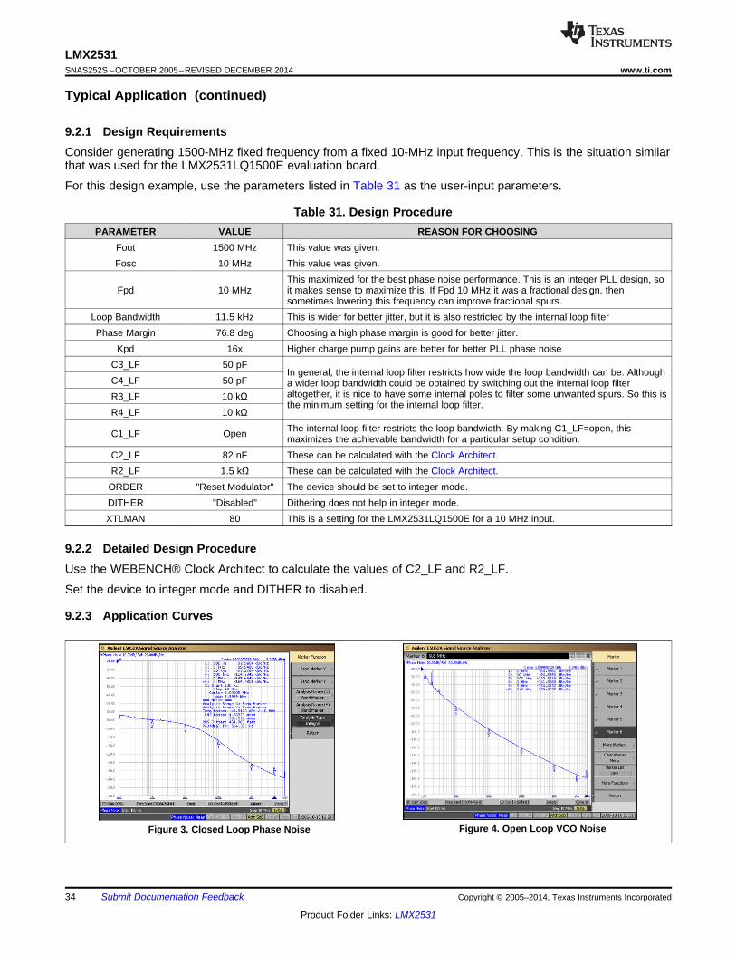
LMX2531SNAS252S –OCTOBER 2005–REVISED DECEMBER 2014 www.ti.com
Typical Application (continued)
9.2.1 Design RequirementsConsider generating 1500-MHz fixed frequency from a fixed 10-MHz input frequency. This is the situation similarthat was used for the LMX2531LQ1500E evaluation board.
For this design example, use the parameters listed in Table 31 as the user-input parameters.
Table 31. Design ProcedurePARAMETER VALUE REASON FOR CHOOSING
Fout 1500 MHz This value was given.Fosc 10 MHz This value was given.
This maximized for the best phase noise performance. This is an integer PLL design, soFpd 10 MHz it makes sense to maximize this. If Fpd 10 MHz it was a fractional design, then
sometimes lowering this frequency can improve fractional spurs.Loop Bandwidth 11.5 kHz This is wider for better jitter, but it is also restricted by the internal loop filterPhase Margin 76.8 deg Choosing a high phase margin is good for better jitter.
Kpd 16x Higher charge pump gains are better for better PLL phase noiseC3_LF 50 pF
In general, the internal loop filter restricts how wide the loop bandwidth can be. AlthoughC4_LF 50 pF a wider loop bandwidth could be obtained by switching out the internal loop filter
altogether, it is nice to have some internal poles to filter some unwanted spurs. So this isR3_LF 10 kΩthe minimum setting for the internal loop filter.
R4_LF 10 kΩThe internal loop filter restricts the loop bandwidth. By making C1_LF=open, thisC1_LF Open maximizes the achievable bandwidth for a particular setup condition.
C2_LF 82 nF These can be calculated with the Clock Architect.R2_LF 1.5 kΩ These can be calculated with the Clock Architect.
ORDER "Reset Modulator" The device should be set to integer mode.DITHER "Disabled" Dithering does not help in integer mode.XTLMAN 80 This is a setting for the LMX2531LQ1500E for a 10 MHz input.
9.2.2 Detailed Design ProcedureUse the WEBENCH® Clock Architect to calculate the values of C2_LF and R2_LF.
Set the device to integer mode and DITHER to disabled.
9.2.3 Application Curves
Figure 4. Open Loop VCO NoiseFigure 3. Closed Loop Phase Noise
34 Submit Documentation Feedback Copyright © 2005–2014, Texas Instruments Incorporated
Product Folder Links: LMX2531

LMX2531www.ti.com SNAS252S –OCTOBER 2005–REVISED DECEMBER 2014
9.3 Do's and Don'ts
Category Do Don't WhyMaximizing the charge pump current andphase detector frequency give the best PLL
For Fractional Designs: phase noise and also allow a widerFor integer Designs: Blindly maximize charge pump bandwidth with the internal filter engaged.Loop Filter Design Maximize charge pump current current and phase detector However, increasing these also increase theand phase detector frequency. frequency. integer boundary spur. So for a fractionaldesign, these need to be balanced againstfractional spurs.
Be aware that engaging this can Design for the widest possible Enabling the internal loop filter polesPartially Integrated restrict the loop filter bandwidth. bandwidth with the integrated provides useful filtering, but also restrictsLoop Filter Use TI simulation tools to see filter engaged and be surprised how wide the loop bandwidth can be.how wide the bandwidth can be. when the bandwidth is smaller.The DAP is grounded and used. However, ifthe terminal description says "Do notground" this is for a reason. Some of these
Ground the "No Connect" Pins pins are for the VCO tank circuit. There are"No Connect" and Ground the DAP Pin where the pin description says other no connect pins that are true noDAP Pins "Do Not Ground". connect, but there is no advantage togrounding them. Note that the pad labeled"NC" above pins 14 and 15 should NOT begrounded.
10 Power Supply RecommendationsThe device is designed to operate within a recommended supply voltage range of 2.8 V to 3.2 V. Do not exceedthe values listed in the Absolute Maximum Ratings table. If the supply is not available, ensure that the CLK,DATA, LE, and CE pins are held low. A power-on reset (POR) feature is not available for this device.
11 Layout
11.1 Layout GuidelinesFor the layout of the LMX2531, perhaps the most important factor is to be aware of the package footprint. Theasymmetrical land pattern can cause issues if not correctly done.
11.1.1 Typical Connection Diagram
11.1.1.1 VccDIG, VccVCO, VccBUF, and VccPLLThese pins are inputs to voltage regulators. Because the LMX2531 contains internal regulators, the power supplynoise rejection is very good and capacitors at this pin are not critical. An RC filter can be used to reduce supplynoise, but if the capacitor is too large and is placed too close to these pins, they can sometimes cause phasenoise degradation in the 100 — 300 kHz offset range. Recommended values are from open to 1 μF. The 10 Ωseries resistors serve to filter power supply noise and isolate these pins from large capacitances.
11.1.1.2 VregDIGA bypass capacitor of 10 nF is recommended.
11.1.1.3 VrefVCOIf the VrefVCO capacitor is changed, it is recommended to keep this capacitor between 1/100 and 1/1000 of thevalue of the VregVCO capacitor.
11.1.1.4 VregVCOBecause this pin is the output of a regulator, there are stability concerns if there is not sufficient seriesresistance. For ceramic capacitors, the ESR (Equivalent Series Resistance) is too low, and it is recommendedthat a series resistance of 1 — 3.3 Ω is necessary. If there is insufficient ESR, then there may be degradation inthe phase noise, especially in the 100 — 300 kHz offset. Recommended values are from 1 μF to 10 μF.
Copyright © 2005–2014, Texas Instruments Incorporated Submit Documentation Feedback 35
Product Folder Links: LMX2531
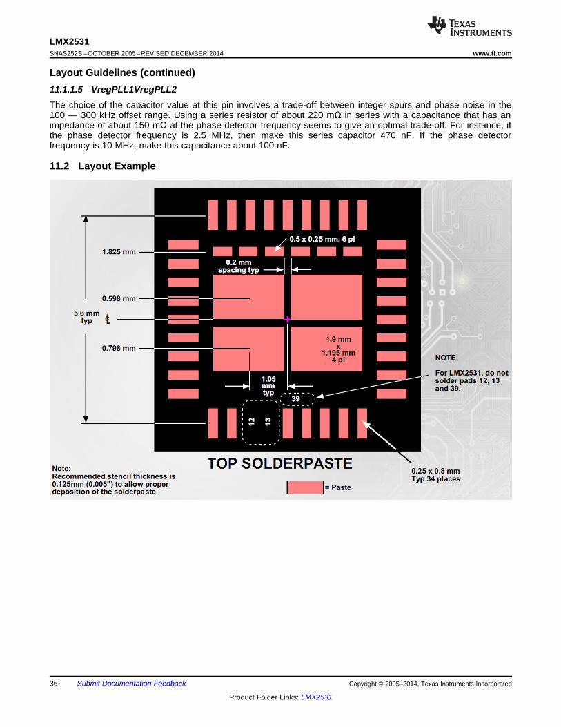
LMX2531SNAS252S –OCTOBER 2005–REVISED DECEMBER 2014 www.ti.com
Layout Guidelines (continued)11.1.1.5 VregPLL1VregPLL2The choice of the capacitor value at this pin involves a trade-off between integer spurs and phase noise in the100 — 300 kHz offset range. Using a series resistor of about 220 mΩ in series with a capacitance that has animpedance of about 150 mΩ at the phase detector frequency seems to give an optimal trade-off. For instance, ifthe phase detector frequency is 2.5 MHz, then make this series capacitor 470 nF. If the phase detectorfrequency is 10 MHz, make this capacitance about 100 nF.
11.2 Layout Example
36 Submit Documentation Feedback Copyright © 2005–2014, Texas Instruments Incorporated
Product Folder Links: LMX2531

LMX2531www.ti.com SNAS252S –OCTOBER 2005–REVISED DECEMBER 2014
12 Device and Documentation Support
12.1 Device SupportFor the Clock Architect tool, go to http://www.ti.com/lsds/ti/analog/webench/clock-architect.page
12.2 TrademarksAll trademarks are the property of their respective owners.
12.3 Electrostatic Discharge CautionThese devices have limited built-in ESD protection. The leads should be shorted together or the device placed in conductive foamduring storage or handling to prevent electrostatic damage to the MOS gates.
12.4 GlossarySLYZ022 — TI Glossary.
This glossary lists and explains terms, acronyms, and definitions.
13 Mechanical, Packaging, and Orderable InformationThe following pages include mechanical, packaging, and orderable information. This information is the mostcurrent data available for the designated devices. This data is subject to change without notice and revision ofthis document. For browser-based versions of this data sheet, refer to the left-hand navigation.
Copyright © 2005–2014, Texas Instruments Incorporated Submit Documentation Feedback 37
Product Folder Links: LMX2531

PACKAGE OPTION ADDENDUM
www.ti.com 7-Jan-2017
Addendum-Page 1
PACKAGING INFORMATION
Orderable Device Status(1)
Package Type PackageDrawing
Pins PackageQty
Eco Plan(2)
Lead/Ball Finish(6)
MSL Peak Temp(3)
Op Temp (°C) Device Marking(4/5)
Samples
LMX2531LQ1146E/NOPB ACTIVE WQFN NJH 36 1000 Green (RoHS& no Sb/Br)
CU SN Level-3-260C-168 HR -40 to 85 311146E
LMX2531LQ1226E/NOPB ACTIVE WQFN NJH 36 1000 Green (RoHS& no Sb/Br)
CU SN Level-3-260C-168 HR -40 to 85 311226E
LMX2531LQ1312E/NOPB ACTIVE WQFN NJH 36 1000 Green (RoHS& no Sb/Br)
CU SN Level-3-260C-168 HR -40 to 85 311312E
LMX2531LQ1415E/NOPB ACTIVE WQFN NJH 36 1000 Green (RoHS& no Sb/Br)
CU SN Level-3-260C-168 HR -40 to 85 311415E
LMX2531LQ1500E/NOPB ACTIVE WQFN NJG 36 250 Green (RoHS& no Sb/Br)
CU SN Level-3-260C-168 HR -40 to 85 311500EB
LMX2531LQ1515E/NOPB ACTIVE WQFN NJH 36 1000 Green (RoHS& no Sb/Br)
CU SN Level-3-260C-168 HR -40 to 85 311515E
LMX2531LQ1570E/NOPB ACTIVE WQFN NJG 36 250 Green (RoHS& no Sb/Br)
CU SN Level-3-260C-168 HR -40 to 85 311570EB
LMX2531LQ1650E/NOPB ACTIVE WQFN NJG 36 250 Green (RoHS& no Sb/Br)
CU SN Level-3-260C-168 HR -40 to 85 311650EA
LMX2531LQ1700E/NOPB ACTIVE WQFN NJG 36 250 Green (RoHS& no Sb/Br)
CU SN Level-3-260C-168 HR -40 to 85 311700EB
LMX2531LQ1742/NOPB ACTIVE WQFN NJG 36 250 Green (RoHS& no Sb/Br)
CU SN Level-3-260C-168 HR -40 to 85 311742A
LMX2531LQ1778E/NOPB ACTIVE WQFN NJG 36 250 Green (RoHS& no Sb/Br)
CU SN Level-3-260C-168 HR -40 to 85 311778EA
LMX2531LQ1910E/NOPB ACTIVE WQFN NJG 36 250 Green (RoHS& no Sb/Br)
CU SN Level-3-260C-168 HR -40 to 85 311910EB
LMX2531LQ2080E/NOPB ACTIVE WQFN NJG 36 250 Green (RoHS& no Sb/Br)
CU SN Level-3-260C-168 HR -40 to 85 312080EB
LMX2531LQ2265E/NOPB ACTIVE WQFN NJG 36 250 Green (RoHS& no Sb/Br)
CU SN Level-3-260C-168 HR -40 to 85 312265ED
LMX2531LQ2570E/NOPB ACTIVE WQFN NJG 36 250 Green (RoHS& no Sb/Br)
CU SN Level-3-260C-168 HR -40 to 85 312570EC
LMX2531LQ2820E/NOPB ACTIVE WQFN NJH 36 1000 Green (RoHS& no Sb/Br)
CU SN Level-3-260C-168 HR -40 to 85 312820E
LMX2531LQ3010E/NOPB ACTIVE WQFN NJH 36 1000 Green (RoHS& no Sb/Br)
CU SN Level-3-260C-168 HR -40 to 85 313010E

PACKAGE OPTION ADDENDUM
www.ti.com 7-Jan-2017
Addendum-Page 2
Orderable Device Status(1)
Package Type PackageDrawing
Pins PackageQty
Eco Plan(2)
Lead/Ball Finish(6)
MSL Peak Temp(3)
Op Temp (°C) Device Marking(4/5)
Samples
LMX2531LQE1146E/NOPB ACTIVE WQFN NJH 36 250 Green (RoHS& no Sb/Br)
CU SN Level-3-260C-168 HR -40 to 85 311146E
LMX2531LQE1226E/NOPB ACTIVE WQFN NJH 36 250 Green (RoHS& no Sb/Br)
CU SN Level-3-260C-168 HR -40 to 85 311226E
LMX2531LQE1312E/NOPB ACTIVE WQFN NJH 36 250 Green (RoHS& no Sb/Br)
CU SN Level-3-260C-168 HR -40 to 85 311312E
LMX2531LQE1415E/NOPB ACTIVE WQFN NJH 36 250 Green (RoHS& no Sb/Br)
CU SN Level-3-260C-168 HR -40 to 85 311415E
LMX2531LQE1515E/NOPB ACTIVE WQFN NJH 36 250 Green (RoHS& no Sb/Br)
CU SN Level-3-260C-168 HR -40 to 85 311515E
LMX2531LQE2820E/NOPB ACTIVE WQFN NJH 36 250 Green (RoHS& no Sb/Br)
CU SN Level-3-260C-168 HR -40 to 85 312820E
LMX2531LQE3010E/NOPB ACTIVE WQFN NJH 36 250 Green (RoHS& no Sb/Br)
CU SN Level-3-260C-168 HR -40 to 85 313010E
LMX2531LQX1146E/NOPB ACTIVE WQFN NJH 36 2500 Green (RoHS& no Sb/Br)
CU SN Level-3-260C-168 HR -40 to 85 311146E
LMX2531LQX1226E/NOPB ACTIVE WQFN NJH 36 2500 Green (RoHS& no Sb/Br)
CU SN Level-3-260C-168 HR -40 to 85 311226E
LMX2531LQX1312E/NOPB ACTIVE WQFN NJH 36 2500 Green (RoHS& no Sb/Br)
CU SN Level-3-260C-168 HR -40 to 85 311312E
LMX2531LQX1415E/NOPB ACTIVE WQFN NJH 36 2500 Green (RoHS& no Sb/Br)
CU SN Level-3-260C-168 HR -40 to 85 311415E
LMX2531LQX1500E/NOPB ACTIVE WQFN NJG 36 2500 Green (RoHS& no Sb/Br)
CU SN Level-3-260C-168 HR -40 to 85 311500EB
LMX2531LQX1515E/NOPB ACTIVE WQFN NJH 36 2500 Green (RoHS& no Sb/Br)
CU SN Level-3-260C-168 HR -40 to 85 311515E
LMX2531LQX1570E/NOPB ACTIVE WQFN NJG 36 2500 Green (RoHS& no Sb/Br)
CU SN Level-3-260C-168 HR -40 to 85 311570EB
LMX2531LQX1650E/NOPB ACTIVE WQFN NJG 36 2500 Green (RoHS& no Sb/Br)
CU SN Level-3-260C-168 HR -40 to 85 311650EA
LMX2531LQX1700E/NOPB ACTIVE WQFN NJG 36 2500 Green (RoHS& no Sb/Br)
CU SN Level-3-260C-168 HR -40 to 85 311700EB
LMX2531LQX1742/NOPB ACTIVE WQFN NJG 36 2500 Green (RoHS& no Sb/Br)
CU SN Level-3-260C-168 HR -40 to 85 311742A
LMX2531LQX1778E/NOPB ACTIVE WQFN NJG 36 2500 Green (RoHS& no Sb/Br)
CU SN Level-3-260C-168 HR -40 to 85 311778EA
PACKAGE OPTION ADDENDUM
www.ti.com 7-Jan-2017
Addendum-Page 3
Orderable Device Status(1)
Package Type PackageDrawing
Pins PackageQty
Eco Plan(2)
Lead/Ball Finish(6)
MSL Peak Temp(3)
Op Temp (°C) Device Marking(4/5)
Samples
LMX2531LQX1910E/NOPB ACTIVE WQFN NJG 36 2500 Green (RoHS& no Sb/Br)
CU SN Level-3-260C-168 HR -40 to 85 311910EB
LMX2531LQX2080E/NOPB ACTIVE WQFN NJG 36 2500 Green (RoHS& no Sb/Br)
CU SN Level-3-260C-168 HR -40 to 85 312080EB
LMX2531LQX2265E/NOPB ACTIVE WQFN NJG 36 2500 Green (RoHS& no Sb/Br)
CU SN Level-3-260C-168 HR -40 to 85 312265ED
LMX2531LQX2570E/NOPB ACTIVE WQFN NJG 36 2500 Green (RoHS& no Sb/Br)
CU SN Level-3-260C-168 HR -40 to 85 312570EC
LMX2531LQX2820E/NOPB ACTIVE WQFN NJH 36 2500 Green (RoHS& no Sb/Br)
CU SN Level-3-260C-168 HR -40 to 85 312820E
LMX2531LQX3010E/NOPB ACTIVE WQFN NJH 36 2500 Green (RoHS& no Sb/Br)
CU SN Level-3-260C-168 HR -40 to 85 313010E
(1) The marketing status values are defined as follows:ACTIVE: Product device recommended for new designs.LIFEBUY: TI has announced that the device will be discontinued, and a lifetime-buy period is in effect.NRND: Not recommended for new designs. Device is in production to support existing customers, but TI does not recommend using this part in a new design.PREVIEW: Device has been announced but is not in production. Samples may or may not be available.OBSOLETE: TI has discontinued the production of the device.
(2) Eco Plan - The planned eco-friendly classification: Pb-Free (RoHS), Pb-Free (RoHS Exempt), or Green (RoHS & no Sb/Br) - please check http://www.ti.com/productcontent for the latest availabilityinformation and additional product content details.TBD: The Pb-Free/Green conversion plan has not been defined.Pb-Free (RoHS): TI's terms "Lead-Free" or "Pb-Free" mean semiconductor products that are compatible with the current RoHS requirements for all 6 substances, including the requirement thatlead not exceed 0.1% by weight in homogeneous materials. Where designed to be soldered at high temperatures, TI Pb-Free products are suitable for use in specified lead-free processes.Pb-Free (RoHS Exempt): This component has a RoHS exemption for either 1) lead-based flip-chip solder bumps used between the die and package, or 2) lead-based die adhesive used betweenthe die and leadframe. The component is otherwise considered Pb-Free (RoHS compatible) as defined above.Green (RoHS & no Sb/Br): TI defines "Green" to mean Pb-Free (RoHS compatible), and free of Bromine (Br) and Antimony (Sb) based flame retardants (Br or Sb do not exceed 0.1% by weightin homogeneous material)
(3) MSL, Peak Temp. - The Moisture Sensitivity Level rating according to the JEDEC industry standard classifications, and peak solder temperature.
(4) There may be additional marking, which relates to the logo, the lot trace code information, or the environmental category on the device.
(5) Multiple Device Markings will be inside parentheses. Only one Device Marking contained in parentheses and separated by a "~" will appear on a device. If a line is indented then it is a continuationof the previous line and the two combined represent the entire Device Marking for that device.

PACKAGE OPTION ADDENDUM
www.ti.com 7-Jan-2017
Addendum-Page 4
(6) Lead/Ball Finish - Orderable Devices may have multiple material finish options. Finish options are separated by a vertical ruled line. Lead/Ball Finish values may wrap to two lines if the finishvalue exceeds the maximum column width.
Important Information and Disclaimer:The information provided on this page represents TI's knowledge and belief as of the date that it is provided. TI bases its knowledge and belief on informationprovided by third parties, and makes no representation or warranty as to the accuracy of such information. Efforts are underway to better integrate information from third parties. TI has taken andcontinues to take reasonable steps to provide representative and accurate information but may not have conducted destructive testing or chemical analysis on incoming materials and chemicals.TI and TI suppliers consider certain information to be proprietary, and thus CAS numbers and other limited information may not be available for release.
In no event shall TI's liability arising out of such information exceed the total purchase price of the TI part(s) at issue in this document sold by TI to Customer on an annual basis.

TAPE AND REEL INFORMATION
*All dimensions are nominal
Device PackageType
PackageDrawing
Pins SPQ ReelDiameter
(mm)
ReelWidth
W1 (mm)
A0(mm)
B0(mm)
K0(mm)
P1(mm)
W(mm)
Pin1Quadrant
LMX2531LQ1146E/NOPB WQFN NJH 36 1000 330.0 16.4 6.3 6.3 1.5 12.0 16.0 Q1
LMX2531LQ1226E/NOPB WQFN NJH 36 1000 330.0 16.4 6.3 6.3 1.5 12.0 16.0 Q1
LMX2531LQ1312E/NOPB WQFN NJH 36 1000 330.0 16.4 6.3 6.3 1.5 12.0 16.0 Q1
LMX2531LQ1415E/NOPB WQFN NJH 36 1000 330.0 16.4 6.3 6.3 1.5 12.0 16.0 Q1
LMX2531LQ1500E/NOPB WQFN NJG 36 250 178.0 16.4 6.3 6.3 1.5 12.0 16.0 Q1
LMX2531LQ1515E/NOPB WQFN NJH 36 1000 330.0 16.4 6.3 6.3 1.5 12.0 16.0 Q1
LMX2531LQ1570E/NOPB WQFN NJG 36 250 178.0 16.4 6.3 6.3 1.5 12.0 16.0 Q1
LMX2531LQ1650E/NOPB WQFN NJG 36 250 178.0 16.4 6.3 6.3 1.5 12.0 16.0 Q1
LMX2531LQ1700E/NOPB WQFN NJG 36 250 178.0 16.4 6.3 6.3 1.5 12.0 16.0 Q1
LMX2531LQ1742/NOPB WQFN NJG 36 250 178.0 16.4 6.3 6.3 1.5 12.0 16.0 Q1
LMX2531LQ1778E/NOPB WQFN NJG 36 250 178.0 16.4 6.3 6.3 1.5 12.0 16.0 Q1
LMX2531LQ1910E/NOPB WQFN NJG 36 250 178.0 16.4 6.3 6.3 1.5 12.0 16.0 Q1
LMX2531LQ2080E/NOPB WQFN NJG 36 250 178.0 16.4 6.3 6.3 1.5 12.0 16.0 Q1
LMX2531LQ2265E/NOPB WQFN NJG 36 250 178.0 16.4 6.3 6.3 1.5 12.0 16.0 Q1
LMX2531LQ2570E/NOPB WQFN NJG 36 250 178.0 16.4 6.3 6.3 1.5 12.0 16.0 Q1
LMX2531LQ2820E/NOPB WQFN NJH 36 1000 330.0 16.4 6.3 6.3 1.5 12.0 16.0 Q1
LMX2531LQ3010E/NOPB WQFN NJH 36 1000 330.0 16.4 6.3 6.3 1.5 12.0 16.0 Q1
LMX2531LQE1146E/NOP WQFN NJH 36 250 178.0 16.4 6.3 6.3 1.5 12.0 16.0 Q1
PACKAGE MATERIALS INFORMATION
www.ti.com 18-May-2017
Pack Materials-Page 1
Device PackageType
PackageDrawing
Pins SPQ ReelDiameter
(mm)
ReelWidth
W1 (mm)
A0(mm)
B0(mm)
K0(mm)
P1(mm)
W(mm)
Pin1Quadrant
B
LMX2531LQE1226E/NOPB
WQFN NJH 36 250 178.0 16.4 6.3 6.3 1.5 12.0 16.0 Q1
LMX2531LQE1312E/NOPB
WQFN NJH 36 250 178.0 16.4 6.3 6.3 1.5 12.0 16.0 Q1
LMX2531LQE1415E/NOPB
WQFN NJH 36 250 178.0 16.4 6.3 6.3 1.5 12.0 16.0 Q1
LMX2531LQE1515E/NOPB
WQFN NJH 36 250 178.0 16.4 6.3 6.3 1.5 12.0 16.0 Q1
LMX2531LQE2820E/NOPB
WQFN NJH 36 250 178.0 16.4 6.3 6.3 1.5 12.0 16.0 Q1
LMX2531LQE3010E/NOPB
WQFN NJH 36 250 178.0 16.4 6.3 6.3 1.5 12.0 16.0 Q1
LMX2531LQX1146E/NOPB
WQFN NJH 36 2500 330.0 16.4 6.3 6.3 1.5 12.0 16.0 Q1
LMX2531LQX1226E/NOPB
WQFN NJH 36 2500 330.0 16.4 6.3 6.3 1.5 12.0 16.0 Q1
LMX2531LQX1312E/NOPB
WQFN NJH 36 2500 330.0 16.4 6.3 6.3 1.5 12.0 16.0 Q1
LMX2531LQX1415E/NOPB
WQFN NJH 36 2500 330.0 16.4 6.3 6.3 1.5 12.0 16.0 Q1
LMX2531LQX1500E/NOPB
WQFN NJG 36 2500 330.0 16.4 6.3 6.3 1.5 12.0 16.0 Q1
LMX2531LQX1515E/NOPB
WQFN NJH 36 2500 330.0 16.4 6.3 6.3 1.5 12.0 16.0 Q1
LMX2531LQX1570E/NOPB
WQFN NJG 36 2500 330.0 16.4 6.3 6.3 1.5 12.0 16.0 Q1
LMX2531LQX1650E/NOPB
WQFN NJG 36 2500 330.0 16.4 6.3 6.3 1.5 12.0 16.0 Q1
LMX2531LQX1700E/NOPB
WQFN NJG 36 2500 330.0 16.4 6.3 6.3 1.5 12.0 16.0 Q1
LMX2531LQX1742/NOPB WQFN NJG 36 2500 330.0 16.4 6.3 6.3 1.5 12.0 16.0 Q1
LMX2531LQX1778E/NOPB
WQFN NJG 36 2500 330.0 16.4 6.3 6.3 1.5 12.0 16.0 Q1
LMX2531LQX1910E/NOPB
WQFN NJG 36 2500 330.0 16.4 6.3 6.3 1.5 12.0 16.0 Q1
LMX2531LQX2080E/NOPB
WQFN NJG 36 2500 330.0 16.4 6.3 6.3 1.5 12.0 16.0 Q1
LMX2531LQX2265E/NOPB
WQFN NJG 36 2500 330.0 16.4 6.3 6.3 1.5 12.0 16.0 Q1
LMX2531LQX2570E/NOPB
WQFN NJG 36 2500 330.0 16.4 6.3 6.3 1.5 12.0 16.0 Q1
LMX2531LQX2820E/NOPB
WQFN NJH 36 2500 330.0 16.4 6.3 6.3 1.5 12.0 16.0 Q1
LMX2531LQX3010E/NOPB
WQFN NJH 36 2500 330.0 16.4 6.3 6.3 1.5 12.0 16.0 Q1
PACKAGE MATERIALS INFORMATION
www.ti.com 18-May-2017
Pack Materials-Page 2
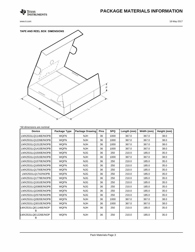
*All dimensions are nominal
Device Package Type Package Drawing Pins SPQ Length (mm) Width (mm) Height (mm)
LMX2531LQ1146E/NOPB WQFN NJH 36 1000 367.0 367.0 38.0
LMX2531LQ1226E/NOPB WQFN NJH 36 1000 367.0 367.0 38.0
LMX2531LQ1312E/NOPB WQFN NJH 36 1000 367.0 367.0 38.0
LMX2531LQ1415E/NOPB WQFN NJH 36 1000 367.0 367.0 38.0
LMX2531LQ1500E/NOPB WQFN NJG 36 250 210.0 185.0 35.0
LMX2531LQ1515E/NOPB WQFN NJH 36 1000 367.0 367.0 38.0
LMX2531LQ1570E/NOPB WQFN NJG 36 250 210.0 185.0 35.0
LMX2531LQ1650E/NOPB WQFN NJG 36 250 210.0 185.0 35.0
LMX2531LQ1700E/NOPB WQFN NJG 36 250 210.0 185.0 35.0
LMX2531LQ1742/NOPB WQFN NJG 36 250 210.0 185.0 35.0
LMX2531LQ1778E/NOPB WQFN NJG 36 250 210.0 185.0 35.0
LMX2531LQ1910E/NOPB WQFN NJG 36 250 210.0 185.0 35.0
LMX2531LQ2080E/NOPB WQFN NJG 36 250 210.0 185.0 35.0
LMX2531LQ2265E/NOPB WQFN NJG 36 250 210.0 185.0 35.0
LMX2531LQ2570E/NOPB WQFN NJG 36 250 210.0 185.0 35.0
LMX2531LQ2820E/NOPB WQFN NJH 36 1000 367.0 367.0 38.0
LMX2531LQ3010E/NOPB WQFN NJH 36 1000 367.0 367.0 38.0
LMX2531LQE1146E/NOPB
WQFN NJH 36 250 210.0 185.0 35.0
LMX2531LQE1226E/NOPB
WQFN NJH 36 250 210.0 185.0 35.0
PACKAGE MATERIALS INFORMATION
www.ti.com 18-May-2017
Pack Materials-Page 3
Device Package Type Package Drawing Pins SPQ Length (mm) Width (mm) Height (mm)
LMX2531LQE1312E/NOPB
WQFN NJH 36 250 210.0 185.0 35.0
LMX2531LQE1415E/NOPB
WQFN NJH 36 250 210.0 185.0 35.0
LMX2531LQE1515E/NOPB
WQFN NJH 36 250 210.0 185.0 35.0
LMX2531LQE2820E/NOPB
WQFN NJH 36 250 210.0 185.0 35.0
LMX2531LQE3010E/NOPB
WQFN NJH 36 250 210.0 185.0 35.0
LMX2531LQX1146E/NOPB
WQFN NJH 36 2500 367.0 367.0 38.0
LMX2531LQX1226E/NOPB
WQFN NJH 36 2500 367.0 367.0 38.0
LMX2531LQX1312E/NOPB
WQFN NJH 36 2500 367.0 367.0 38.0
LMX2531LQX1415E/NOPB
WQFN NJH 36 2500 367.0 367.0 38.0
LMX2531LQX1500E/NOPB
WQFN NJG 36 2500 367.0 367.0 38.0
LMX2531LQX1515E/NOPB
WQFN NJH 36 2500 367.0 367.0 38.0
LMX2531LQX1570E/NOPB
WQFN NJG 36 2500 367.0 367.0 38.0
LMX2531LQX1650E/NOPB
WQFN NJG 36 2500 367.0 367.0 38.0
LMX2531LQX1700E/NOPB
WQFN NJG 36 2500 367.0 367.0 38.0
LMX2531LQX1742/NOPB WQFN NJG 36 2500 367.0 367.0 38.0
LMX2531LQX1778E/NOPB
WQFN NJG 36 2500 367.0 367.0 38.0
LMX2531LQX1910E/NOPB
WQFN NJG 36 2500 367.0 367.0 38.0
LMX2531LQX2080E/NOPB
WQFN NJG 36 2500 367.0 367.0 38.0
LMX2531LQX2265E/NOPB
WQFN NJG 36 2500 367.0 367.0 38.0
LMX2531LQX2570E/NOPB
WQFN NJG 36 2500 367.0 367.0 38.0
LMX2531LQX2820E/NOPB
WQFN NJH 36 2500 367.0 367.0 38.0
LMX2531LQX3010E/NOPB
WQFN NJH 36 2500 367.0 367.0 38.0
PACKAGE MATERIALS INFORMATION
www.ti.com 18-May-2017
Pack Materials-Page 4

MECHANICAL DATA
NJG0036A
www.ti.com
LQA36A (Rev C)
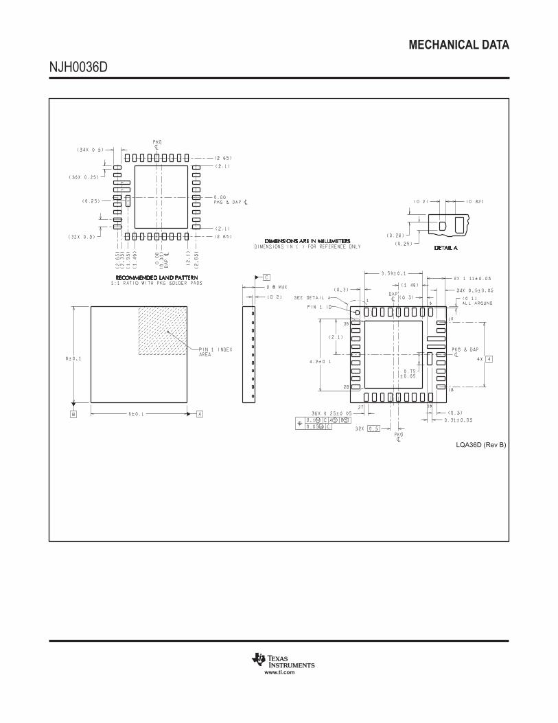
MECHANICAL DATA
NJH0036D
www.ti.com
LQA36D (Rev B)

IMPORTANT NOTICE
Texas Instruments Incorporated (TI) reserves the right to make corrections, enhancements, improvements and other changes to itssemiconductor products and services per JESD46, latest issue, and to discontinue any product or service per JESD48, latest issue. Buyersshould obtain the latest relevant information before placing orders and should verify that such information is current and complete.TI’s published terms of sale for semiconductor products (http://www.ti.com/sc/docs/stdterms.htm) apply to the sale of packaged integratedcircuit products that TI has qualified and released to market. Additional terms may apply to the use or sale of other types of TI products andservices.Reproduction of significant portions of TI information in TI data sheets is permissible only if reproduction is without alteration and isaccompanied by all associated warranties, conditions, limitations, and notices. TI is not responsible or liable for such reproduceddocumentation. Information of third parties may be subject to additional restrictions. Resale of TI products or services with statementsdifferent from or beyond the parameters stated by TI for that product or service voids all express and any implied warranties for theassociated TI product or service and is an unfair and deceptive business practice. TI is not responsible or liable for any such statements.Buyers and others who are developing systems that incorporate TI products (collectively, “Designers”) understand and agree that Designersremain responsible for using their independent analysis, evaluation and judgment in designing their applications and that Designers havefull and exclusive responsibility to assure the safety of Designers' applications and compliance of their applications (and of all TI productsused in or for Designers’ applications) with all applicable regulations, laws and other applicable requirements. Designer represents that, withrespect to their applications, Designer has all the necessary expertise to create and implement safeguards that (1) anticipate dangerousconsequences of failures, (2) monitor failures and their consequences, and (3) lessen the likelihood of failures that might cause harm andtake appropriate actions. Designer agrees that prior to using or distributing any applications that include TI products, Designer willthoroughly test such applications and the functionality of such TI products as used in such applications.TI’s provision of technical, application or other design advice, quality characterization, reliability data or other services or information,including, but not limited to, reference designs and materials relating to evaluation modules, (collectively, “TI Resources”) are intended toassist designers who are developing applications that incorporate TI products; by downloading, accessing or using TI Resources in anyway, Designer (individually or, if Designer is acting on behalf of a company, Designer’s company) agrees to use any particular TI Resourcesolely for this purpose and subject to the terms of this Notice.TI’s provision of TI Resources does not expand or otherwise alter TI’s applicable published warranties or warranty disclaimers for TIproducts, and no additional obligations or liabilities arise from TI providing such TI Resources. TI reserves the right to make corrections,enhancements, improvements and other changes to its TI Resources. TI has not conducted any testing other than that specificallydescribed in the published documentation for a particular TI Resource.Designer is authorized to use, copy and modify any individual TI Resource only in connection with the development of applications thatinclude the TI product(s) identified in such TI Resource. NO OTHER LICENSE, EXPRESS OR IMPLIED, BY ESTOPPEL OR OTHERWISETO ANY OTHER TI INTELLECTUAL PROPERTY RIGHT, AND NO LICENSE TO ANY TECHNOLOGY OR INTELLECTUAL PROPERTYRIGHT OF TI OR ANY THIRD PARTY IS GRANTED HEREIN, including but not limited to any patent right, copyright, mask work right, orother intellectual property right relating to any combination, machine, or process in which TI products or services are used. Informationregarding or referencing third-party products or services does not constitute a license to use such products or services, or a warranty orendorsement thereof. Use of TI Resources may require a license from a third party under the patents or other intellectual property of thethird party, or a license from TI under the patents or other intellectual property of TI.TI RESOURCES ARE PROVIDED “AS IS” AND WITH ALL FAULTS. TI DISCLAIMS ALL OTHER WARRANTIES ORREPRESENTATIONS, EXPRESS OR IMPLIED, REGARDING RESOURCES OR USE THEREOF, INCLUDING BUT NOT LIMITED TOACCURACY OR COMPLETENESS, TITLE, ANY EPIDEMIC FAILURE WARRANTY AND ANY IMPLIED WARRANTIES OFMERCHANTABILITY, FITNESS FOR A PARTICULAR PURPOSE, AND NON-INFRINGEMENT OF ANY THIRD PARTY INTELLECTUALPROPERTY RIGHTS. TI SHALL NOT BE LIABLE FOR AND SHALL NOT DEFEND OR INDEMNIFY DESIGNER AGAINST ANY CLAIM,INCLUDING BUT NOT LIMITED TO ANY INFRINGEMENT CLAIM THAT RELATES TO OR IS BASED ON ANY COMBINATION OFPRODUCTS EVEN IF DESCRIBED IN TI RESOURCES OR OTHERWISE. IN NO EVENT SHALL TI BE LIABLE FOR ANY ACTUAL,DIRECT, SPECIAL, COLLATERAL, INDIRECT, PUNITIVE, INCIDENTAL, CONSEQUENTIAL OR EXEMPLARY DAMAGES INCONNECTION WITH OR ARISING OUT OF TI RESOURCES OR USE THEREOF, AND REGARDLESS OF WHETHER TI HAS BEENADVISED OF THE POSSIBILITY OF SUCH DAMAGES.Unless TI has explicitly designated an individual product as meeting the requirements of a particular industry standard (e.g., ISO/TS 16949and ISO 26262), TI is not responsible for any failure to meet such industry standard requirements.Where TI specifically promotes products as facilitating functional safety or as compliant with industry functional safety standards, suchproducts are intended to help enable customers to design and create their own applications that meet applicable functional safety standardsand requirements. Using products in an application does not by itself establish any safety features in the application. Designers mustensure compliance with safety-related requirements and standards applicable to their applications. Designer may not use any TI products inlife-critical medical equipment unless authorized officers of the parties have executed a special contract specifically governing such use.Life-critical medical equipment is medical equipment where failure of such equipment would cause serious bodily injury or death (e.g., lifesupport, pacemakers, defibrillators, heart pumps, neurostimulators, and implantables). Such equipment includes, without limitation, allmedical devices identified by the U.S. Food and Drug Administration as Class III devices and equivalent classifications outside the U.S.TI may expressly designate certain products as completing a particular qualification (e.g., Q100, Military Grade, or Enhanced Product).Designers agree that it has the necessary expertise to select the product with the appropriate qualification designation for their applicationsand that proper product selection is at Designers’ own risk. Designers are solely responsible for compliance with all legal and regulatoryrequirements in connection with such selection.Designer will fully indemnify TI and its representatives against any damages, costs, losses, and/or liabilities arising out of Designer’s non-compliance with the terms and provisions of this Notice.
Mailing Address: Texas Instruments, Post Office Box 655303, Dallas, Texas 75265Copyright © 2017, Texas Instruments Incorporated