
LMV331 Single, LMV393 Dual, LMV339 Quad GENERAL-PURPOSE LOW-VOLTAGE COMPARATORS datasheet (Rev....
42
+ – IN– IN+ OUT Product Folder Sample & Buy Technical Documents Tools & Software Support & Community LMV331, LMV393, LMV339 SLCS136T – AUGUST 1999 – REVISED JANUARY 2015 LMV331 Single, LMV393 Dual, LMV339 Quad General-purpose Low-voltage Comparators 1 Features 3 Description The LMV393 and LMV339 devices are low-voltage 1• 2.7-V and 5-V Performance (2.7 V to 5.5 V) versions of the dual and quad • Low Supply Current comparators, LM393 and LM339, which operate from – LMV331 130 μA Typ 5 V to 30 V. The LMV331 is the single-comparator version. – LMV393 210 μA Typ – LMV339 410 μA Typ The LMV331, LMV339, and LMV393 are the most cost-effective solutions for applications where low- • Input Common-Mode Voltage Range Includes voltage operation, low power, and space saving are Ground the primary specifications in circuit design for portable • Low Output Saturation Voltage 200 mV Typical consumer products. These devices offer • Open-Collector Output for Maximum Flexibility specifications that meet or exceed the familiar LM339 and LM393 devices at a fraction of the supply current. 2 Applications Device Information (1) • Hysteresis Comparators PART NUMBER PACKAGE (PIN) BODY SIZE (NOM) • Oscillators LMV339 SOIC (14) 8.65 mm x 3.90 mm • Window Comparators LMV393 SOIC (8) 4.90 mm x 3.90 mm • Industrial Equipment LMV331 SC70 (5) 2.00 mm x 1.25 mm • Test and Measurement (1) For all available packages, see the orderable addendum at the end of the datasheet. 4 Simplified Schematic 1 An IMPORTANT NOTICE at the end of this data sheet addresses availability, warranty, changes, use in safety-critical applications, intellectual property matters and other important disclaimers. PRODUCTION DATA.
Transcript of LMV331 Single, LMV393 Dual, LMV339 Quad GENERAL-PURPOSE LOW-VOLTAGE COMPARATORS datasheet (Rev....

+
–
IN–
IN+
OUT
Product
Folder
Sample &Buy
Technical
Documents
Tools &
Software
Support &Community
LMV331, LMV393, LMV339SLCS136T –AUGUST 1999–REVISED JANUARY 2015
LMV331 Single, LMV393 Dual, LMV339 Quad General-purpose Low-voltage Comparators1 Features 3 Description
The LMV393 and LMV339 devices are low-voltage1• 2.7-V and 5-V Performance
(2.7 V to 5.5 V) versions of the dual and quad• Low Supply Current comparators, LM393 and LM339, which operate from– LMV331 130 μA Typ 5 V to 30 V. The LMV331 is the single-comparator
version.– LMV393 210 μA Typ– LMV339 410 μA Typ The LMV331, LMV339, and LMV393 are the most
cost-effective solutions for applications where low-• Input Common-Mode Voltage Range Includesvoltage operation, low power, and space saving areGroundthe primary specifications in circuit design for portable
• Low Output Saturation Voltage 200 mV Typical consumer products. These devices offer• Open-Collector Output for Maximum Flexibility specifications that meet or exceed the familiar LM339
and LM393 devices at a fraction of the supply current.2 Applications
Device Information(1)• Hysteresis Comparators
PART NUMBER PACKAGE (PIN) BODY SIZE (NOM)• Oscillators
LMV339 SOIC (14) 8.65 mm x 3.90 mm• Window Comparators LMV393 SOIC (8) 4.90 mm x 3.90 mm• Industrial Equipment LMV331 SC70 (5) 2.00 mm x 1.25 mm• Test and Measurement (1) For all available packages, see the orderable addendum at
the end of the datasheet.
4 Simplified Schematic
1
An IMPORTANT NOTICE at the end of this data sheet addresses availability, warranty, changes, use in safety-critical applications,intellectual property matters and other important disclaimers. PRODUCTION DATA.
LMV331, LMV393, LMV339SLCS136T –AUGUST 1999–REVISED JANUARY 2015 www.ti.com
Table of Contents8.1 Overview .................................................................. 91 Features .................................................................. 18.2 Functional Block Diagram ......................................... 92 Applications ........................................................... 18.3 Feature Description................................................... 93 Description ............................................................. 18.4 Device Functional Modes.......................................... 94 Simplified Schematic............................................. 1
9 Application and Implementation ........................ 105 Revision History..................................................... 29.1 Application Information............................................ 106 Pin Configuration and Functions ......................... 39.2 Typical Application ................................................. 107 Specifications......................................................... 4 10 Power Supply Recommendations ..................... 127.1 Absolute Maximum Ratings ...................................... 4
11 Layout................................................................... 127.2 ESD Ratings.............................................................. 411.1 Layout Guidelines ................................................. 127.3 Recommended Operating Conditions....................... 411.2 Layout Example .................................................... 127.4 Thermal Information .................................................. 4
12 Device and Documentation Support ................. 137.5 Electrical Characteristics, VCC+ = 2.7 V .................... 512.1 Related Links ........................................................ 137.6 Electrical Characteristics, VCC+ = 5 V ....................... 612.2 Trademarks ........................................................... 137.7 Switching Characteristics, VCC+ = 2.7 V ................... 612.3 Electrostatic Discharge Caution............................ 137.8 Switching Characteristics, VCC+ = 5 V ...................... 612.4 Glossary ................................................................ 137.9 Typical Characteristics .............................................. 7
13 Mechanical, Packaging, and Orderable8 Detailed Description .............................................. 9Information ........................................................... 13
5 Revision History
Changes from Revision S (October 2012) to Revision T Page
• Added Applications, Device Information table, Pin Functions table, ESD Ratings table, Thermal Information table,Typical Characteristics, Feature Description section, Device Functional Modes, Application and Implementationsection, Power Supply Recommendations section, Layout section, Device and Documentation Support section, andMechanical, Packaging, and Orderable Information section. ................................................................................................. 1
• Deleted Ordering Information table. ....................................................................................................................................... 1
Changes from Revision R (May 2012) to Revision S Page
• Updated operating temperature range. .................................................................................................................................. 4
Changes from Revision N (April 2011) to Revision O Page
• Changed VI in the Absolute Maximum Ratings from 5.5 V to VCC+ ....................................................................................... 4
Changes from Revision M (November 2005) to Revision N Page
• Changed document format from Quicksilver to DocZone. ..................................................................................................... 1• Added RUC package pin out drawing. ................................................................................................................................... 3
2 Submit Documentation Feedback Copyright © 1999–2015, Texas Instruments Incorporated
1
2
3
4
5
6
7
14
13
12
11
10
9
8
2OUT
1OUT
1IN–
VCC+
1IN+
2IN–
2IN+
3OUT
3IN–
4IN+
GND
4IN–
3IN+
4OUT
LMV339 . . . D OR PW PACKAGE
(TOP VIEW)
LMV393 . . . D, DDU, DGK OR PW PACKAGE
(TOP VIEW)
1
2
3
4
8
7
6
5
1OUT
1IN–
1IN+
GND
VCC+
2OUT
2IN–
2IN+
LMV331 . . . DBV OR DCK PACKAGE
(TOP VIEW)
VCC+
OUT
1
2
3
5
4
1IN+
GND
1IN–
LMV339 . . . RUC PACKAGE
(TOP VIEW)
1
2
3
4
5
12
11
10
9
876
14 131OUT
1IN–
VCC+
1IN+
2IN–
2IN
+
3IN
–
4IN+
GND
4IN–
3IN+
4OUT
3O
UT
2O
UT
LMV331, LMV393, LMV339www.ti.com SLCS136T –AUGUST 1999–REVISED JANUARY 2015
6 Pin Configuration and Functions
Pin FunctionsPIN
LMV331 LMV393 LMV339 TYPE DESCRIPTIONNAME DBV or D, DDU, D or PW RUCDCK DGK or PW1IN– ,2IN–, 3 2, 6 4, 6, 8, 10 3, 5, 7, 9 I Comparator(s) negative input pin(s)3IN–,4IN–1IN+ ,2IN+, 1 3, 5 5, 7, 9, 11 4, 6, 8, 10 I Comparator(s) positive input pin(s)3IN+,4IN+GND 2 4 12 11 I Ground1OUT,2OUT, 4 1, 7 2, 1, 14, 13 1, 14, 13, 12 O Comparator(s) output pin(s)3OUT,4OUTVCC+ 5 8 3 2 I Supply Pin
Copyright © 1999–2015, Texas Instruments Incorporated Submit Documentation Feedback 3

LMV331, LMV393, LMV339SLCS136T –AUGUST 1999–REVISED JANUARY 2015 www.ti.com
7 Specifications
7.1 Absolute Maximum Ratingsover operating free-air temperature range (unless otherwise noted) (1)
MIN MAX UNITVCC Supply voltage (2) 5.5 VVID Differential input voltage (3) ±5.5 VVI Input voltage range (either input) 0 VCC+ V
At or below TA = 25°C,Duration of output short circuit (one amplifier) to ground (4) UnlimitedVCC ≤ 5.5 VTJ Operating virtual junction temperature 150 °CTstg Storage temperature range –65 150 °C
(1) Stresses beyond those listed under Absolute Maximum Ratings may cause permanent damage to the device. These are stress ratingsonly, and functional operation of the device at these or any other conditions beyond those indicated under Recommended OperatingConditions is not implied. Exposure to absolute-maximum-rated conditions for extended periods may affect device reliability.
(2) All voltage values (except differential voltages and VCC specified for the measurement of IOS) are with respect to the network GND.(3) Differential voltages are at IN+ with respect to IN–.(4) Short circuits from outputs to VCC can cause excessive heating and eventual destruction.
7.2 ESD RatingsVALUE UNIT
Human body model (HBM), per ANSI/ESDA/JEDEC JS-001, all pins (1) ±2000V(ESD) Electrostatic discharge VCharged device model (CDM), per JEDEC specification JESD22-C101, ±1000all pins (2)
(1) JEDEC document JEP155 states that 500-V HBM allows safe manufacturing with a standard ESD control process.(2) JEDEC document JEP157 states that 250-V CDM allows safe manufacturing with a standard ESD control process.
7.3 Recommended Operating ConditionsMIN MAX UNIT
VCC Supply voltage (single-supply operation) 2.7 5.5 VVOUT Output voltage VCC+ + 0.3 VTA Operating free-air temperature –40 125 °C
7.4 Thermal InformationLMV339 LMV393 LMV331
THERMAL METRIC (1) D PW RUC D DDU DGK PW DBV DCK UNIT
14 PINS 8 PINS 5 PINS
RθJA Junction-to-ambient 86 113 216 97 210 172 149 206 252thermal resistance
RθJC(top) Junction-to-case (top) — — 51.3 — — — — — —thermal resistance
RθJB Junction-to-board — — 59.0 — — — — — —thermal resistance °C/WψJT Junction-to-top
characterization — — 1.2 — — — — — —parameter
ψJB Junction-to-boardcharacterization — — 59.0 — — — — — —parameter
(1) For more information about traditional and new thermal metrics, see the IC Package Thermal Metrics application report, SPRA953.
4 Submit Documentation Feedback Copyright © 1999–2015, Texas Instruments Incorporated

LMV331, LMV393, LMV339www.ti.com SLCS136T –AUGUST 1999–REVISED JANUARY 2015
7.5 Electrical Characteristics, VCC+ = 2.7 VVCC+ = 2.7 V, GND = 0 V, at specified free-air temperature (unless otherwise noted)
PARAMETER TEST CONDITIONS TA MIN TYP MAX UNITVIO Input offset voltage 25°C 1.7 7 mV
Average temperature –40°C toαVIO coefficient of input offset 5 μV/°C125°Cvoltage25°C 15 250
IIB Input bias current nA–40°C to 400125°C25°C 5 50
IIO Input offset current nA–40°C to 150125°CIO Output current (sinking) VO ≤ 1.5 V 25°C 5 23 mA
25°C 0.003Output Leakage Current µA–40°C to 1125°CCommon-mode inputVICR 25°C –0.1 to 2 Vvoltage range
VSAT Saturation voltage IO ≤ 1.5 mA 25°C 200 mVLMV331 25°C 40 100
ICC Supply current LMV393 (both comparators) 25°C 70 140 μALMV339 (all four comparators) 25°C 140 200
Copyright © 1999–2015, Texas Instruments Incorporated Submit Documentation Feedback 5
LMV331, LMV393, LMV339SLCS136T –AUGUST 1999–REVISED JANUARY 2015 www.ti.com
7.6 Electrical Characteristics, VCC+ = 5 VVCC+ = 5 V, GND = 0 V, at specified free-air temperature (unless otherwise noted)
PARAMETER TEST CONDITIONS TA MIN TYP MAX UNIT25°C 1.7 7
VIO Input offset voltage mV–40°C to 9125°CAverage temperature
αVIO coefficient of input offset 25°C 5 μV/°Cvoltage
25°C 25 250IIB Input bias current nA–40°C to 400125°C
25°C 2 50IIO Input offset current nA–40°C to 150125°CIO Output current (sinking) VO ≤ 1.5 V 25°C 10 84 mA
25°C 0.003Output Leakage Current µA–40°C to 1125°CCommon-mode inputVICR 25°C –0.1 to 4.2 Vvoltage rangeLarge-signal differentialAVD 25°C 20 50 V/mVvoltage gain
25°C 200 400VSAT Saturation voltage IO ≤ 4 mA mV–40°C to 700125°C
25°C 60 120LMV331 –40°C to 150125°C
25°C 100 200ICC Supply current LMV393 (both comparators) μA–40°C to 250125°C
25°C 170 300LMV339 (all four comparators) –40°C to 350125°C
7.7 Switching Characteristics, VCC+ = 2.7 VTA = 25°C, VCC+ = 2.7 V, RL = 5.1 kΩ, GND = 0 V (unless otherwise noted)
PARAMETER TEST CONDITIONS TYP UNITInput overdrive = 10 mV 1000Propagation delay high to low level outputtPHL nsswitching Input overdrive = 100 mV 350Input overdrive = 10 mV 500Propagation delay low to high level outputtPLH nsswitching Input overdrive = 100 mV 400
7.8 Switching Characteristics, VCC+ = 5 VTA = 25°C, VCC+ = 5 V, RL = 5.1 kΩ, GND = 0 V (unless otherwise noted)
PARAMETER TEST CONDITIONS TYP UNITInput overdrive = 10 mV 600Propagation delay high to low level outputtPHL nsswitching Input overdrive = 100 mV 200Input overdrive = 10 mV 450Propagation delay low to high level outputtPLH nsswitching Input overdrive = 100 mV 300
6 Submit Documentation Feedback Copyright © 1999–2015, Texas Instruments Incorporated
Overdrive (mV)
Tim
e (n
s)
0 10 20 30 40 50 60 70 80 90 100265
270
275
280
285
290
295
300
305
310
Overdrive (mV)
Tim
e (n
s)
0 10 20 30 40 50 60 70 80 90 100172.5
172.8
173.1
173.4
173.7
174
174.3
174.6
174.9
175.2
175.5
175.8
176.1
Output Current (mA)
Out
put V
olta
ge (
mV
)
0 5 10 15 20 25 30 35 40 45 50100
150
200
250
300
350
400
450
500
550
600
650
700-40C25C85C
Supply Voltage (V)
Inpu
t Bia
s C
urre
nt (
nA)
2.4 2.7 3 3.3 3.6 3.9 4.2 4.5 4.8 5.1 5.4 5.725
27.5
30
32.5
35
37.5
40
42.5
45
47.5
50
52.5
55-40C25C85C
Volts (V)
Sup
pply
Cur
rent
(P
A)
1 1.5 2 2.5 3 3.5 4 4.5 505
10152025303540455055606570
-40C25C85C
Volts (V)
Sup
pply
Cur
rent
(P
A)
1 1.5 2 2.5 3 3.5 4 4.5 5253035404550556065707580859095
-40C25C85C
LMV331, LMV393, LMV339www.ti.com SLCS136T –AUGUST 1999–REVISED JANUARY 2015
7.9 Typical CharacteristicsUnless otherwise specified, VS = +5V, single supply, TA = 25°C
Figure 1. Supply Current vs Supply Voltage Output High Figure 2. Supply Current vs Supply Voltage Output Low(LMV33x) (LMV33x)
Figure 3. Output Voltage vs Output Current Figure 4. Input Bias Current vs Supply Voltage
Figure 5. Response Time vs Input Overdrives Negative Figure 6. Response Time vs Input Overdrives PositiveTransition (VCC=5 V) Transition (VCC = 5 V)
Copyright © 1999–2015, Texas Instruments Incorporated Submit Documentation Feedback 7
Overdrive (mV)
Tim
e (n
s)
0 10 20 30 40 50 60 70 80 90 100612
615
618
621
624
627
630
633
636
639
642
645
648
Overdrive (mV)
Tim
e (n
s)
0 10 20 30 40 50 60 70 80 90 100185.4
185.7
186
186.3
186.6
186.9
187.2
187.5
187.8
188.1
188.4
188.7
189
LMV331, LMV393, LMV339SLCS136T –AUGUST 1999–REVISED JANUARY 2015 www.ti.com
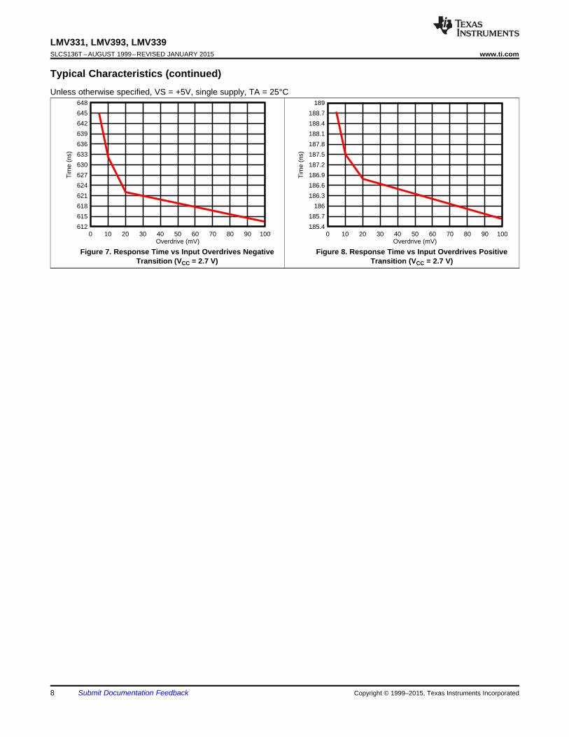
Typical Characteristics (continued)Unless otherwise specified, VS = +5V, single supply, TA = 25°C
Figure 7. Response Time vs Input Overdrives Negative Figure 8. Response Time vs Input Overdrives PositiveTransition (VCC = 2.7 V) Transition (VCC = 2.7 V)
8 Submit Documentation Feedback Copyright © 1999–2015, Texas Instruments Incorporated

IN+
IN−
OUT
GND
R1
Q1 Q3
Q7Q6
VCC+
Q2 Q4 Q5
R2 R3
Q8
Q9
LMV331, LMV393, LMV339www.ti.com SLCS136T –AUGUST 1999–REVISED JANUARY 2015
8 Detailed Description
8.1 OverviewThe LMV331, LMV393 and LMV339 family of comparators have the ability to operate up to 5 V on the supply pin.This standard device has proven ubiquity and versatility across a wide range of applications. This is due to it'slow Iq and fast response.
The open-drain output allows the user to configure the output's logic low voltage (VOL) and can be utilized toenable the comparator to be used in AND functionality.
8.2 Functional Block Diagram
8.3 Feature DescriptionThe LMV331, LMV393 and LMV339 consists of a PNP input, whose Vbe creates a limit on the input commonmode voltage capability, allowing LMV33x to accurately function from ground to VCC–Vbe(~700mV) differentialinput. This enables much head room for modern day supplies of 3.3 V and 5.0 V.
The output consists of an open drain NPN (pull-down or low side) transistor. The output NPN will sink currentwhen the positive input voltage is higher than the negative input voltage and the offset voltage. The VOL isresistive and will scale with the output current. Please see Figure 3 for VOL values with respect to the outputcurrent.
8.4 Device Functional Modes
8.4.1 Voltage ComparisonThe LMV33x operates solely as a voltage comparator, comparing the differential voltage between the positiveand negative pins and outputs a logic low or high impedance (logic high with pull-up) based on the inputdifferential polarity.
Copyright © 1999–2015, Texas Instruments Incorporated Submit Documentation Feedback 9
+LMV33x
VLOGIC
VSUP
Vref
Vin +LMV33x
Vin-
Vin+
RpullupRpullup
VLOGIC
VSUP
CL CL
LMV331, LMV393, LMV339SLCS136T –AUGUST 1999–REVISED JANUARY 2015 www.ti.com
9 Application and Implementation
NOTEInformation in the following applications sections is not part of the TI componentspecification, and TI does not warrant its accuracy or completeness. TI’s customers areresponsible for determining suitability of components for their purposes. Customers shouldvalidate and test their design implementation to confirm system functionality.
9.1 Application InformationLMV331, LMV393, and LMV339 will typically be used to compare a single signal to a reference or two signalsagainst each other. Many users take advantage of the open drain output to drive the comparison logic output to alogic voltage level to an MCU or logic device. The wide supply range and high voltage capability makes LMV331,LMV393, and LMV33 optimal for level shifting to a higher or lower voltage.
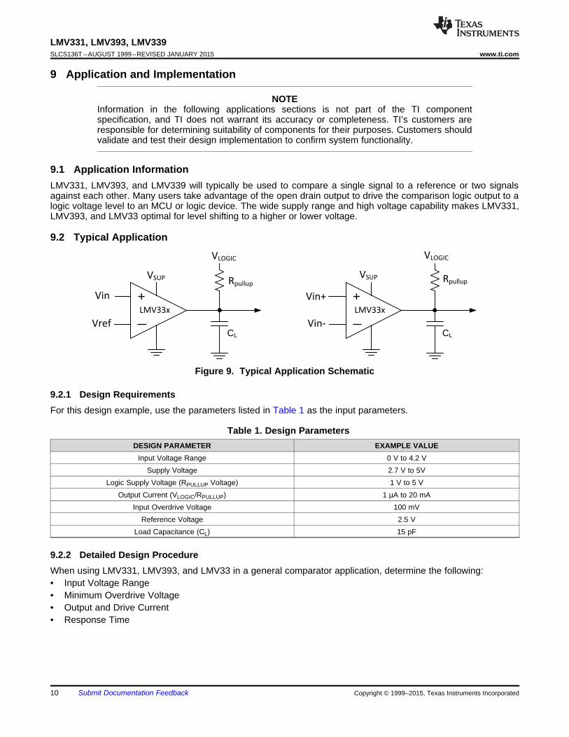
9.2 Typical Application
Figure 9. Typical Application Schematic
9.2.1 Design RequirementsFor this design example, use the parameters listed in Table 1 as the input parameters.
Table 1. Design ParametersDESIGN PARAMETER EXAMPLE VALUE
Input Voltage Range 0 V to 4.2 VSupply Voltage 2.7 V to 5V
Logic Supply Voltage (RPULLUP Voltage) 1 V to 5 VOutput Current (VLOGIC/RPULLUP) 1 µA to 20 mA
Input Overdrive Voltage 100 mVReference Voltage 2.5 V
Load Capacitance (CL) 15 pF
9.2.2 Detailed Design ProcedureWhen using LMV331, LMV393, and LMV33 in a general comparator application, determine the following:• Input Voltage Range• Minimum Overdrive Voltage• Output and Drive Current• Response Time
10 Submit Documentation Feedback Copyright © 1999–2015, Texas Instruments Incorporated
LMV331, LMV393, LMV339www.ti.com SLCS136T –AUGUST 1999–REVISED JANUARY 2015
9.2.2.1 Input Voltage RangeWhen choosing the input voltage range, the input common mode voltage range (VICR) must be taken in toaccount. If operating temperature is above or below 25°C the VICR can range from 0 V to VCC– 0.7 V. This limitsthe input voltage range to as high as VCC– 0.7 V and as low as 0 V. Operation outside of this range can yieldincorrect comparisons.
Below is a possible list of input voltage situation and their outcomes:
1. When both IN- and IN+ are both within the common mode range:(a) If IN- is higher than IN+ and the offset voltage, the output is low and the output transistor is sinking
current(b) If IN- is lower than IN+ and the offset voltage, the output is high impedance and the output transistor is
not conducting2. When IN- is higher than common mode and IN+ is within common mode, the output is low and the output
transistor is sinking current3. When IN+ is higher than common mode and IN- is within common mode, the output is high impedance and
the output transistor is not conducting4. When IN- and IN+ are both higher than common mode, the output is low and the output transistor is sinking
current
9.2.2.2 Minimum Overdrive VoltageOverdrive Voltage is the differential voltage produced between the positive and negative inputs of the comparatorover the offset voltage (VIO). In order to make an accurate comparison; the Overdrive Voltage (VOD) should behigher than the input offset voltage (VIO). Overdrive voltage can also determine the response time of thecomparator, with the response time decreasing with increasing overdrive. Figure 10 show positive and negativeresponse times with respect to overdrive voltage.
9.2.2.3 Output and Drive CurrentOutput current is determined by the pull-up resistance (Rpullup) and Vlogic voltage, refer to Figure 9. The outputcurrent will produce a output low voltage (VOL) from the comparator. In which VOL is proportional to the outputcurrent. Use Figure 3 to determine VOL based on the output current.
The output current can also effect the transient response. More will be explained in the next section.
9.2.2.4 Response TimeThe transient response can be determined by the load capacitance (CL), load/pull-up resistance (RPULLUP) andequivalent collector-emitter resistance (RCE).
• The positive response time (τp) is approximately τP ~ RPULLUP × CL• The negative response time (τN) is approximately τN ~ RCE × CL
– RCE can be determine by taking the slope of Figure 3 in it's linear region at the desired temperature, or bydividing the VOL by Iout
9.2.3 Application CurvesThe following curves were generated with 5 V on VCC and VLogic, RPULLUP = 5.1 kΩ, and 50 pF scope probe.
Copyright © 1999–2015, Texas Instruments Incorporated Submit Documentation Feedback 11

OUT
1IN–
2
IN+ 3 4
VCC5
0.1 Fμ
GND
0.1 Fμ
Ground
Bypass
Capacitor
Positive Supply
Negative Supply or Ground
Ground
Only needed
for dual power
supplies
Time (uS)
Vol
tage
(V
)
0.2 0.22 0.24 0.26 0.28 0.3 0.32 0.34 0.36 0.38 0.4-1
-0.50
0.51
1.52
2.53
3.54
4.55
5.56
5mV OD20mV OD100mV OD
LMV331, LMV393, LMV339SLCS136T –AUGUST 1999–REVISED JANUARY 2015 www.ti.com
Figure 10. Response Time for Various Overdrives(Negative Transition)
10 Power Supply RecommendationsFor fast response and comparison applications with noisy or AC inputs, it is recommended to use a bypasscapacitor on the supply pin to reject any variation on the supply voltage. This variation cause temporaryfluctuations in the comparator's input common mode range and create an inaccurate comparison.
11 Layout
11.1 Layout GuidelinesFor accurate comparator applications without hysteresis it is important maintain a stable power supply withminimized noise and glitches, which can affect the high level input common mode voltage range. In order toachieve this, it is best to add a bypass capacitor between the supply voltage and ground. This should beimplemented on the positive power supply and negative supply (if available). If a negative supply is not beingused, do not put a capacitor between the IC's GND pin and system ground.
11.2 Layout Example
Figure 11. LMV331 Layout Example
12 Submit Documentation Feedback Copyright © 1999–2015, Texas Instruments Incorporated
LMV331, LMV393, LMV339www.ti.com SLCS136T –AUGUST 1999–REVISED JANUARY 2015
12 Device and Documentation Support
12.1 Related LinksThe table below lists quick access links. Categories include technical documents, support and communityresources, tools and software, and quick access to sample or buy.
Table 2. Related LinksTECHNICAL TOOLS & SUPPORT &PARTS PRODUCT FOLDER SAMPLE & BUY DOCUMENTS SOFTWARE COMMUNITY
LMV331 Click here Click here Click here Click here Click hereLMV393 Click here Click here Click here Click here Click hereLMV339 Click here Click here Click here Click here Click here
12.2 TrademarksAll trademarks are the property of their respective owners.
12.3 Electrostatic Discharge CautionThese devices have limited built-in ESD protection. The leads should be shorted together or the device placed in conductive foamduring storage or handling to prevent electrostatic damage to the MOS gates.
12.4 GlossarySLYZ022 — TI Glossary.
This glossary lists and explains terms, acronyms, and definitions.
13 Mechanical, Packaging, and Orderable InformationThe following pages include mechanical, packaging, and orderable information. This information is the mostcurrent data available for the designated devices. This data is subject to change without notice and revision ofthis document. For browser-based versions of this data sheet, refer to the left-hand navigation.
Copyright © 1999–2015, Texas Instruments Incorporated Submit Documentation Feedback 13

PACKAGE OPTION ADDENDUM
www.ti.com 8-Apr-2018
Addendum-Page 1
PACKAGING INFORMATION
Orderable Device Status(1)
Package Type PackageDrawing
Pins PackageQty
Eco Plan(2)
Lead/Ball Finish(6)
MSL Peak Temp(3)
Op Temp (°C) Device Marking(4/5)
Samples
LMV331IDBVR ACTIVE SOT-23 DBV 5 3000 Green (RoHS& no Sb/Br)
CU NIPDAU Level-1-260C-UNLIM -40 to 125 (R1IC, R1II)
LMV331IDBVRE4 ACTIVE SOT-23 DBV 5 3000 Green (RoHS& no Sb/Br)
CU NIPDAU Level-1-260C-UNLIM -40 to 125 (R1IC, R1II)
LMV331IDBVRG4 ACTIVE SOT-23 DBV 5 3000 Green (RoHS& no Sb/Br)
CU NIPDAU Level-1-260C-UNLIM -40 to 125 (R1IC, R1II)
LMV331IDBVT ACTIVE SOT-23 DBV 5 250 Green (RoHS& no Sb/Br)
CU NIPDAU Level-1-260C-UNLIM -40 to 125 (R1IC, R1II)
LMV331IDBVTE4 ACTIVE SOT-23 DBV 5 250 Green (RoHS& no Sb/Br)
CU NIPDAU Level-1-260C-UNLIM -40 to 125 (R1IC, R1II)
LMV331IDBVTG4 ACTIVE SOT-23 DBV 5 250 Green (RoHS& no Sb/Br)
CU NIPDAU Level-1-260C-UNLIM -40 to 125 (R1IC, R1II)
LMV331IDCKR ACTIVE SC70 DCK 5 3000 Green (RoHS& no Sb/Br)
CU NIPDAU |CU NIPDAUAG
Level-1-260C-UNLIM -40 to 125 (R2I, R2K, R2R)
LMV331IDCKRE4 ACTIVE SC70 DCK 5 3000 Green (RoHS& no Sb/Br)
CU NIPDAU Level-1-260C-UNLIM -40 to 125 (R2I, R2K, R2R)
LMV331IDCKRG4 ACTIVE SC70 DCK 5 3000 Green (RoHS& no Sb/Br)
CU NIPDAU Level-1-260C-UNLIM -40 to 125 (R2I, R2K, R2R)
LMV331IDCKT ACTIVE SC70 DCK 5 250 Green (RoHS& no Sb/Br)
CU NIPDAU |CU NIPDAUAG
Level-1-260C-UNLIM -40 to 125 (R2C, R2I, R2R)
LMV331IDCKTE4 ACTIVE SC70 DCK 5 250 Green (RoHS& no Sb/Br)
CU NIPDAU Level-1-260C-UNLIM -40 to 125 (R2C, R2I, R2R)
LMV331IDCKTG4 ACTIVE SC70 DCK 5 250 Green (RoHS& no Sb/Br)
CU NIPDAU Level-1-260C-UNLIM -40 to 125 (R2C, R2I, R2R)
LMV339ID ACTIVE SOIC D 14 50 Green (RoHS& no Sb/Br)
CU NIPDAU Level-1-260C-UNLIM -40 to 125 LMV339I
LMV339IDG4 ACTIVE SOIC D 14 50 Green (RoHS& no Sb/Br)
CU NIPDAU Level-1-260C-UNLIM -40 to 125 LMV339I
LMV339IDR ACTIVE SOIC D 14 2500 Green (RoHS& no Sb/Br)
CU NIPDAU Level-1-260C-UNLIM -40 to 125 LMV339I
LMV339IPW ACTIVE TSSOP PW 14 90 Green (RoHS& no Sb/Br)
CU NIPDAU Level-1-260C-UNLIM -40 to 125 MV339I
LMV339IPWG4 ACTIVE TSSOP PW 14 90 Green (RoHS& no Sb/Br)
CU NIPDAU Level-1-260C-UNLIM -40 to 125 MV339I
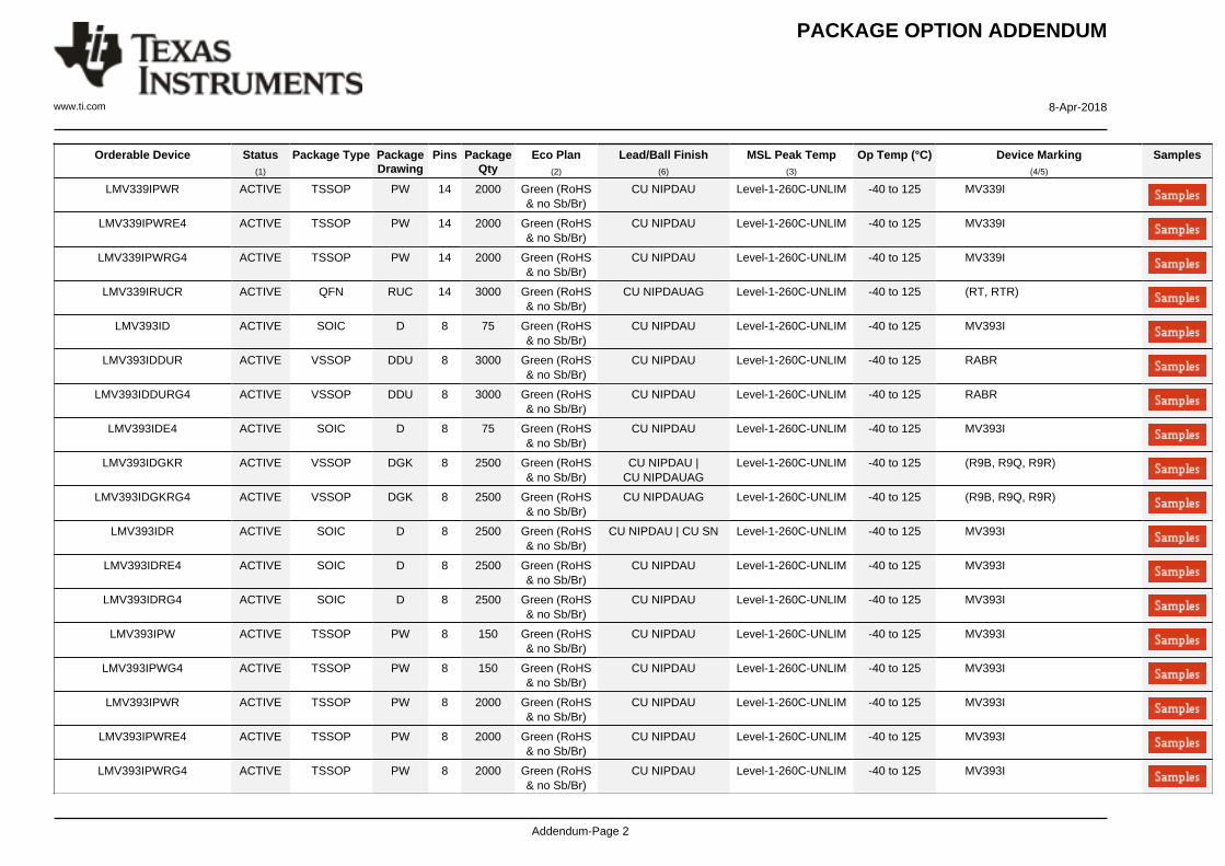
PACKAGE OPTION ADDENDUM
www.ti.com 8-Apr-2018
Addendum-Page 2
Orderable Device Status(1)
Package Type PackageDrawing
Pins PackageQty
Eco Plan(2)
Lead/Ball Finish(6)
MSL Peak Temp(3)
Op Temp (°C) Device Marking(4/5)
Samples
LMV339IPWR ACTIVE TSSOP PW 14 2000 Green (RoHS& no Sb/Br)
CU NIPDAU Level-1-260C-UNLIM -40 to 125 MV339I
LMV339IPWRE4 ACTIVE TSSOP PW 14 2000 Green (RoHS& no Sb/Br)
CU NIPDAU Level-1-260C-UNLIM -40 to 125 MV339I
LMV339IPWRG4 ACTIVE TSSOP PW 14 2000 Green (RoHS& no Sb/Br)
CU NIPDAU Level-1-260C-UNLIM -40 to 125 MV339I
LMV339IRUCR ACTIVE QFN RUC 14 3000 Green (RoHS& no Sb/Br)
CU NIPDAUAG Level-1-260C-UNLIM -40 to 125 (RT, RTR)
LMV393ID ACTIVE SOIC D 8 75 Green (RoHS& no Sb/Br)
CU NIPDAU Level-1-260C-UNLIM -40 to 125 MV393I
LMV393IDDUR ACTIVE VSSOP DDU 8 3000 Green (RoHS& no Sb/Br)
CU NIPDAU Level-1-260C-UNLIM -40 to 125 RABR
LMV393IDDURG4 ACTIVE VSSOP DDU 8 3000 Green (RoHS& no Sb/Br)
CU NIPDAU Level-1-260C-UNLIM -40 to 125 RABR
LMV393IDE4 ACTIVE SOIC D 8 75 Green (RoHS& no Sb/Br)
CU NIPDAU Level-1-260C-UNLIM -40 to 125 MV393I
LMV393IDGKR ACTIVE VSSOP DGK 8 2500 Green (RoHS& no Sb/Br)
CU NIPDAU |CU NIPDAUAG
Level-1-260C-UNLIM -40 to 125 (R9B, R9Q, R9R)
LMV393IDGKRG4 ACTIVE VSSOP DGK 8 2500 Green (RoHS& no Sb/Br)
CU NIPDAUAG Level-1-260C-UNLIM -40 to 125 (R9B, R9Q, R9R)
LMV393IDR ACTIVE SOIC D 8 2500 Green (RoHS& no Sb/Br)
CU NIPDAU | CU SN Level-1-260C-UNLIM -40 to 125 MV393I
LMV393IDRE4 ACTIVE SOIC D 8 2500 Green (RoHS& no Sb/Br)
CU NIPDAU Level-1-260C-UNLIM -40 to 125 MV393I
LMV393IDRG4 ACTIVE SOIC D 8 2500 Green (RoHS& no Sb/Br)
CU NIPDAU Level-1-260C-UNLIM -40 to 125 MV393I
LMV393IPW ACTIVE TSSOP PW 8 150 Green (RoHS& no Sb/Br)
CU NIPDAU Level-1-260C-UNLIM -40 to 125 MV393I
LMV393IPWG4 ACTIVE TSSOP PW 8 150 Green (RoHS& no Sb/Br)
CU NIPDAU Level-1-260C-UNLIM -40 to 125 MV393I
LMV393IPWR ACTIVE TSSOP PW 8 2000 Green (RoHS& no Sb/Br)
CU NIPDAU Level-1-260C-UNLIM -40 to 125 MV393I
LMV393IPWRE4 ACTIVE TSSOP PW 8 2000 Green (RoHS& no Sb/Br)
CU NIPDAU Level-1-260C-UNLIM -40 to 125 MV393I
LMV393IPWRG4 ACTIVE TSSOP PW 8 2000 Green (RoHS& no Sb/Br)
CU NIPDAU Level-1-260C-UNLIM -40 to 125 MV393I

PACKAGE OPTION ADDENDUM
www.ti.com 8-Apr-2018
Addendum-Page 3
(1) The marketing status values are defined as follows:ACTIVE: Product device recommended for new designs.LIFEBUY: TI has announced that the device will be discontinued, and a lifetime-buy period is in effect.NRND: Not recommended for new designs. Device is in production to support existing customers, but TI does not recommend using this part in a new design.PREVIEW: Device has been announced but is not in production. Samples may or may not be available.OBSOLETE: TI has discontinued the production of the device.
(2) RoHS: TI defines "RoHS" to mean semiconductor products that are compliant with the current EU RoHS requirements for all 10 RoHS substances, including the requirement that RoHS substancedo not exceed 0.1% by weight in homogeneous materials. Where designed to be soldered at high temperatures, "RoHS" products are suitable for use in specified lead-free processes. TI mayreference these types of products as "Pb-Free".RoHS Exempt: TI defines "RoHS Exempt" to mean products that contain lead but are compliant with EU RoHS pursuant to a specific EU RoHS exemption.Green: TI defines "Green" to mean the content of Chlorine (Cl) and Bromine (Br) based flame retardants meet JS709B low halogen requirements of <=1000ppm threshold. Antimony trioxide basedflame retardants must also meet the <=1000ppm threshold requirement.
(3) MSL, Peak Temp. - The Moisture Sensitivity Level rating according to the JEDEC industry standard classifications, and peak solder temperature.
(4) There may be additional marking, which relates to the logo, the lot trace code information, or the environmental category on the device.
(5) Multiple Device Markings will be inside parentheses. Only one Device Marking contained in parentheses and separated by a "~" will appear on a device. If a line is indented then it is a continuationof the previous line and the two combined represent the entire Device Marking for that device.
(6) Lead/Ball Finish - Orderable Devices may have multiple material finish options. Finish options are separated by a vertical ruled line. Lead/Ball Finish values may wrap to two lines if the finishvalue exceeds the maximum column width.
Important Information and Disclaimer:The information provided on this page represents TI's knowledge and belief as of the date that it is provided. TI bases its knowledge and belief on informationprovided by third parties, and makes no representation or warranty as to the accuracy of such information. Efforts are underway to better integrate information from third parties. TI has taken andcontinues to take reasonable steps to provide representative and accurate information but may not have conducted destructive testing or chemical analysis on incoming materials and chemicals.TI and TI suppliers consider certain information to be proprietary, and thus CAS numbers and other limited information may not be available for release.
In no event shall TI's liability arising out of such information exceed the total purchase price of the TI part(s) at issue in this document sold by TI to Customer on an annual basis.
OTHER QUALIFIED VERSIONS OF LMV331, LMV393 :
• Automotive: LMV331-Q1, LMV393-Q1
NOTE: Qualified Version Definitions:
• Automotive - Q100 devices qualified for high-reliability automotive applications targeting zero defects

TAPE AND REEL INFORMATION
*All dimensions are nominal
Device PackageType
PackageDrawing
Pins SPQ ReelDiameter
(mm)
ReelWidth
W1 (mm)
A0(mm)
B0(mm)
K0(mm)
P1(mm)
W(mm)
Pin1Quadrant
LMV331IDBVR SOT-23 DBV 5 3000 178.0 9.0 3.23 3.17 1.37 4.0 8.0 Q3
LMV331IDBVT SOT-23 DBV 5 250 178.0 9.0 3.23 3.17 1.37 4.0 8.0 Q3
LMV331IDCKR SC70 DCK 5 3000 180.0 9.2 2.3 2.55 1.2 4.0 8.0 Q3
LMV331IDCKR SC70 DCK 5 3000 178.0 9.0 2.4 2.5 1.2 4.0 8.0 Q3
LMV331IDCKT SC70 DCK 5 250 180.0 9.2 2.3 2.55 1.2 4.0 8.0 Q3
LMV331IDCKT SC70 DCK 5 250 178.0 9.0 2.4 2.5 1.2 4.0 8.0 Q3
LMV339IDR SOIC D 14 2500 330.0 16.4 6.5 9.0 2.1 8.0 16.0 Q1
LMV339IPWR TSSOP PW 14 2000 330.0 12.4 6.9 5.6 1.6 8.0 12.0 Q1
LMV339IRUCR QFN RUC 14 3000 180.0 8.4 2.3 2.3 0.55 4.0 8.0 Q2
LMV393IDDUR VSSOP DDU 8 3000 180.0 8.4 2.25 3.35 1.05 4.0 8.0 Q3
LMV393IDGKR VSSOP DGK 8 2500 330.0 12.4 5.3 3.4 1.4 8.0 12.0 Q1
LMV393IDR SOIC D 8 2500 330.0 12.4 6.4 5.2 2.1 8.0 12.0 Q1
LMV393IDR SOIC D 8 2500 330.0 12.8 6.4 5.2 2.1 8.0 12.0 Q1
LMV393IDRG4 SOIC D 8 2500 330.0 12.4 6.4 5.2 2.1 8.0 12.0 Q1
LMV393IPWR TSSOP PW 8 2000 330.0 12.4 7.0 3.6 1.6 8.0 12.0 Q1
PACKAGE MATERIALS INFORMATION
www.ti.com 3-Aug-2017
Pack Materials-Page 1
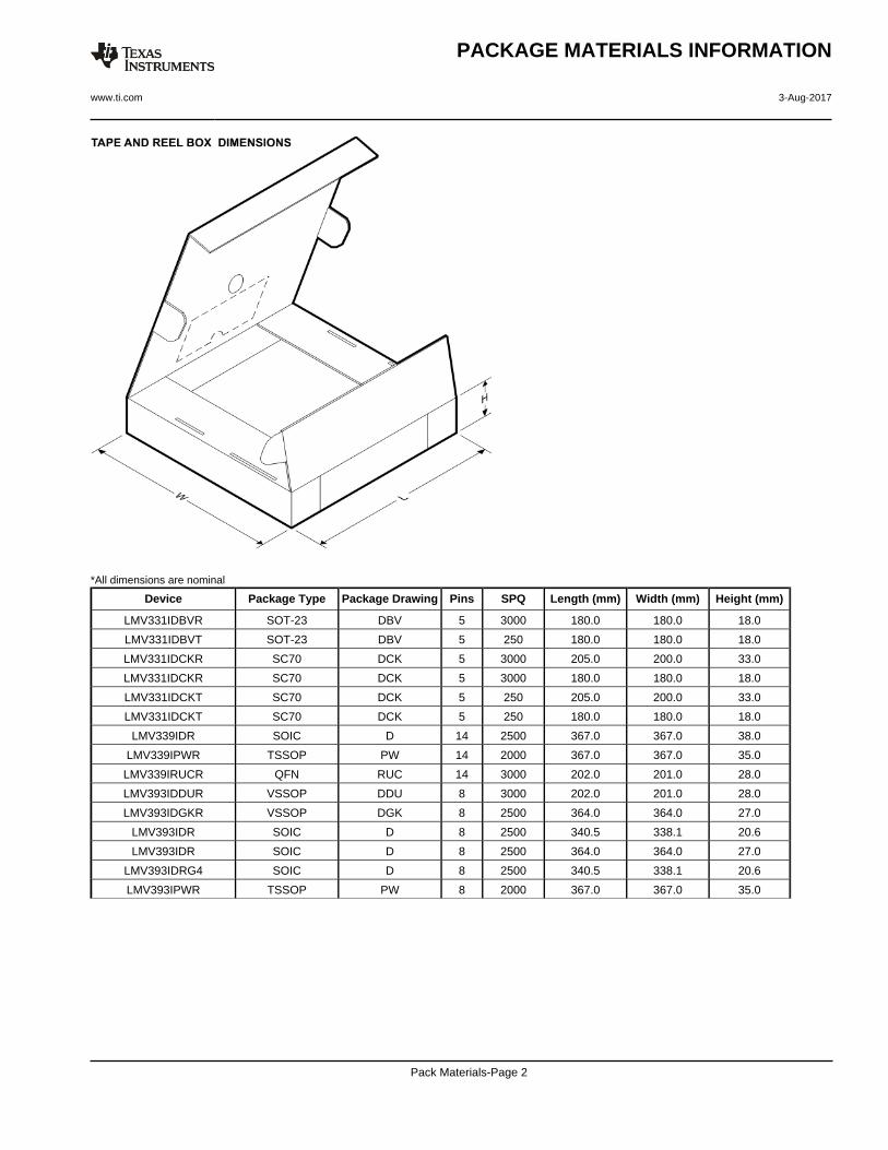
*All dimensions are nominal
Device Package Type Package Drawing Pins SPQ Length (mm) Width (mm) Height (mm)
LMV331IDBVR SOT-23 DBV 5 3000 180.0 180.0 18.0
LMV331IDBVT SOT-23 DBV 5 250 180.0 180.0 18.0
LMV331IDCKR SC70 DCK 5 3000 205.0 200.0 33.0
LMV331IDCKR SC70 DCK 5 3000 180.0 180.0 18.0
LMV331IDCKT SC70 DCK 5 250 205.0 200.0 33.0
LMV331IDCKT SC70 DCK 5 250 180.0 180.0 18.0
LMV339IDR SOIC D 14 2500 367.0 367.0 38.0
LMV339IPWR TSSOP PW 14 2000 367.0 367.0 35.0
LMV339IRUCR QFN RUC 14 3000 202.0 201.0 28.0
LMV393IDDUR VSSOP DDU 8 3000 202.0 201.0 28.0
LMV393IDGKR VSSOP DGK 8 2500 364.0 364.0 27.0
LMV393IDR SOIC D 8 2500 340.5 338.1 20.6
LMV393IDR SOIC D 8 2500 364.0 364.0 27.0
LMV393IDRG4 SOIC D 8 2500 340.5 338.1 20.6
LMV393IPWR TSSOP PW 8 2000 367.0 367.0 35.0
PACKAGE MATERIALS INFORMATION
www.ti.com 3-Aug-2017
Pack Materials-Page 2


www.ti.com
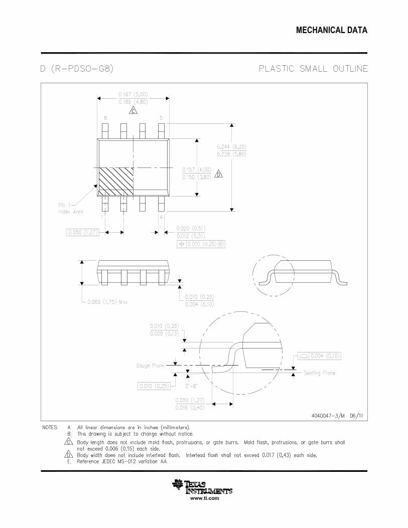
PACKAGE OUTLINE
C
TYP0.220.08
0.25
3.02.6
2X 0.95
1.9
1.45 MAX
TYP0.150.00
5X 0.50.3
TYP0.60.3
TYP80
1.9
A
3.052.75
B1.751.45
(1.1)
SOT-23 - 1.45 mm max heightDBV0005ASMALL OUTLINE TRANSISTOR
4214839/C 04/2017
NOTES: 1. All linear dimensions are in millimeters. Any dimensions in parenthesis are for reference only. Dimensioning and tolerancing per ASME Y14.5M.2. This drawing is subject to change without notice.3. Refernce JEDEC MO-178.
0.2 C A B
1
34
5
2
INDEX AREAPIN 1
GAGE PLANE
SEATING PLANE
0.1 C
SCALE 4.000

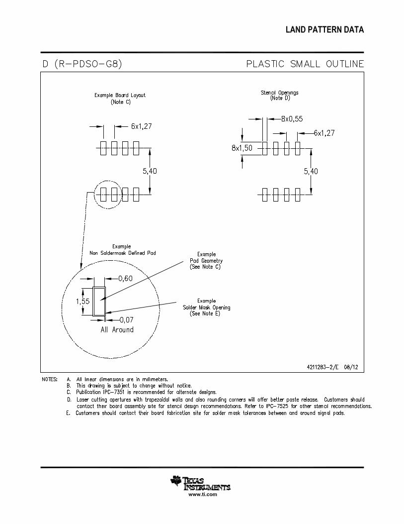
www.ti.com
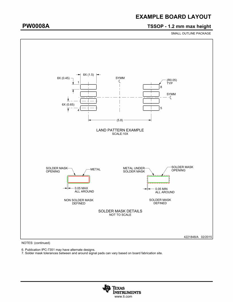
EXAMPLE BOARD LAYOUT
0.07 MAXARROUND
0.07 MINARROUND
5X (1.1)
5X (0.6)
(2.6)
(1.9)
2X (0.95)
(R0.05) TYP
4214839/C 04/2017
SOT-23 - 1.45 mm max heightDBV0005ASMALL OUTLINE TRANSISTOR
NOTES: (continued) 4. Publication IPC-7351 may have alternate designs. 5. Solder mask tolerances between and around signal pads can vary based on board fabrication site.
SYMM
LAND PATTERN EXAMPLEEXPOSED METAL SHOWN
SCALE:15X
PKG
1
3 4
5
2
SOLDER MASKOPENINGMETAL UNDER
SOLDER MASK
SOLDER MASKDEFINED
EXPOSED METAL
METALSOLDER MASKOPENING
NON SOLDER MASKDEFINED
(PREFERRED)
SOLDER MASK DETAILS
EXPOSED METAL

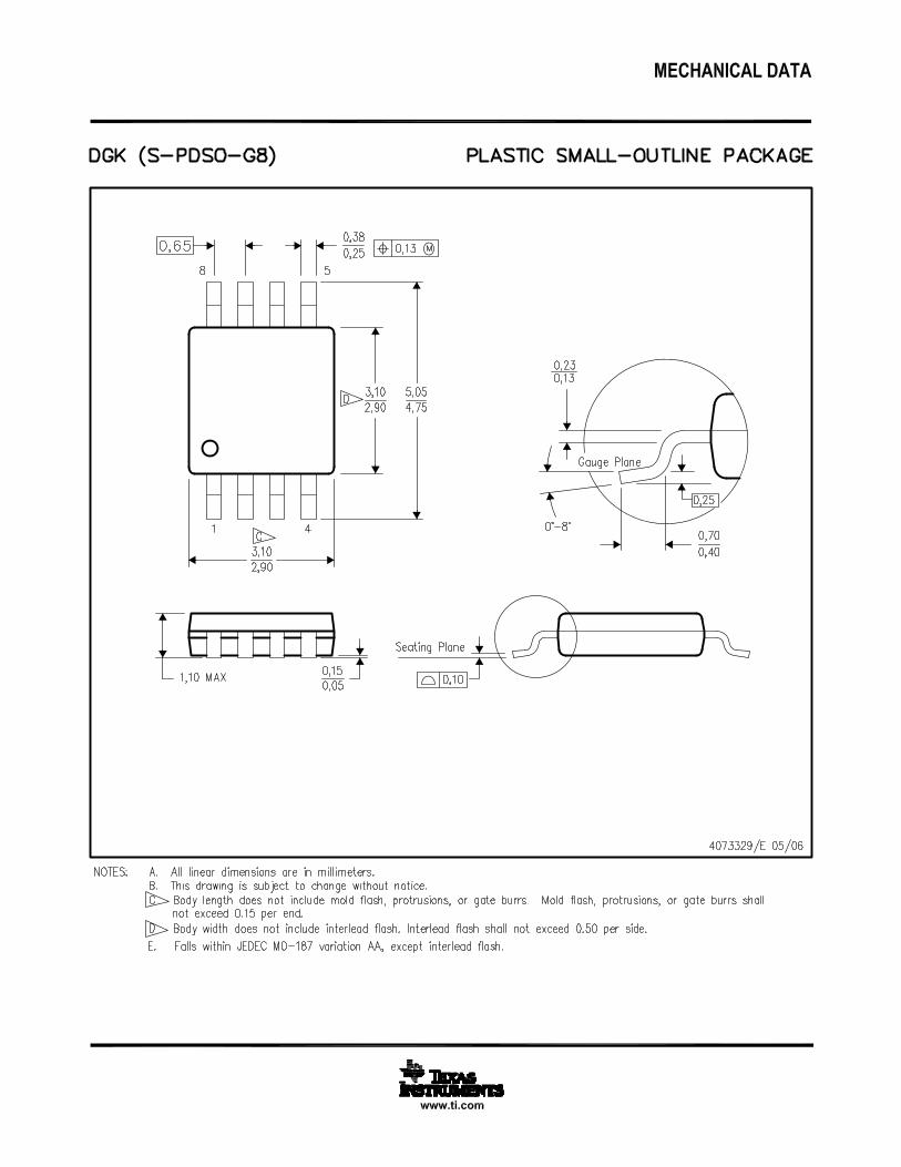
www.ti.com
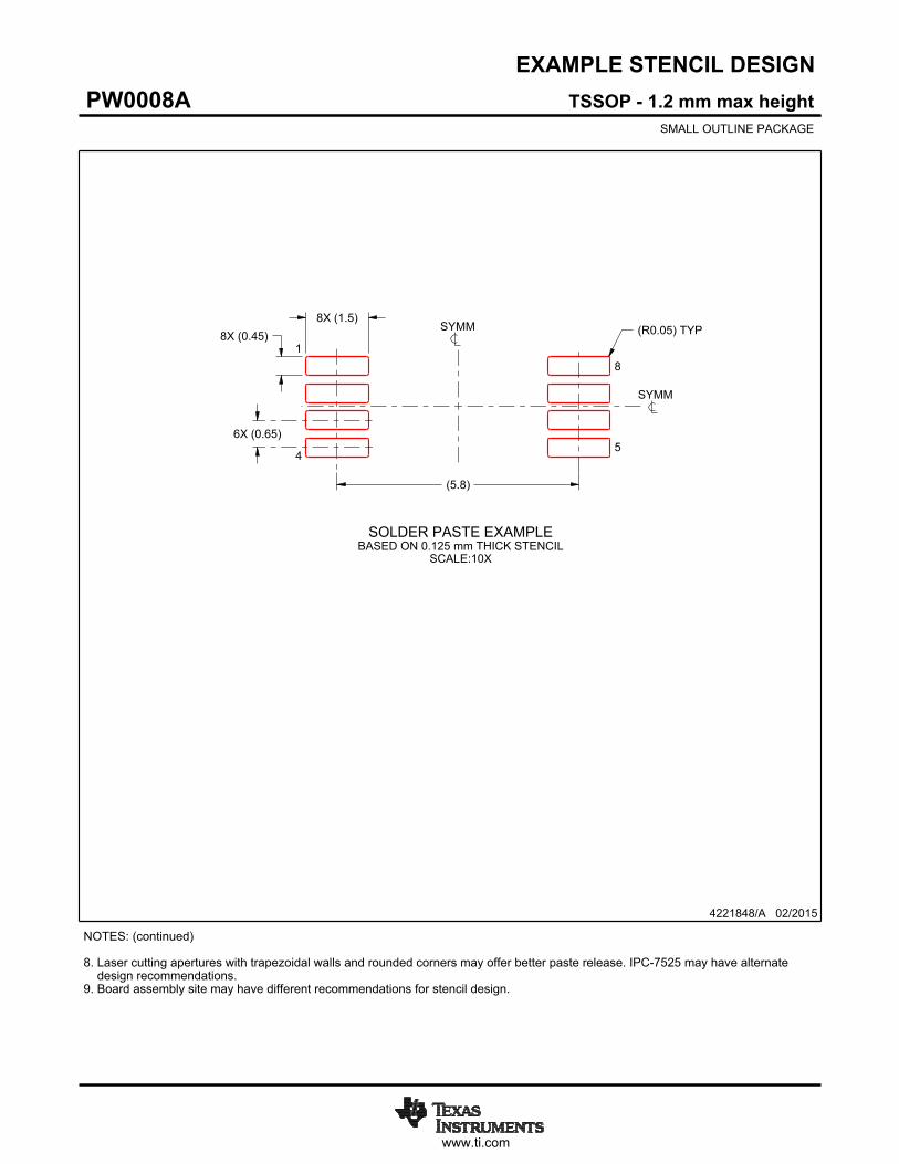
EXAMPLE STENCIL DESIGN
(2.6)
(1.9)
2X(0.95)
5X (1.1)
5X (0.6)
(R0.05) TYP
SOT-23 - 1.45 mm max heightDBV0005ASMALL OUTLINE TRANSISTOR
4214839/C 04/2017
NOTES: (continued) 6. Laser cutting apertures with trapezoidal walls and rounded corners may offer better paste release. IPC-7525 may have alternate design recommendations. 7. Board assembly site may have different recommendations for stencil design.
SOLDER PASTE EXAMPLEBASED ON 0.125 mm THICK STENCIL
SCALE:15X
SYMM
PKG
1
3 4
5
2

www.ti.com
PACKAGE OUTLINE
C
TYP0.220.08
0.25
3.02.6
2X 0.95
1.9
1.45 MAX
TYP0.150.00
5X 0.50.3
TYP0.60.3
TYP80
1.9
A
3.052.75
B1.751.45
(1.1)
SOT-23 - 1.45 mm max heightDBV0005ASMALL OUTLINE TRANSISTOR
4214839/C 04/2017
NOTES: 1. All linear dimensions are in millimeters. Any dimensions in parenthesis are for reference only. Dimensioning and tolerancing per ASME Y14.5M.2. This drawing is subject to change without notice.3. Refernce JEDEC MO-178.
0.2 C A B
1
34
5
2
INDEX AREAPIN 1
GAGE PLANE
SEATING PLANE
0.1 C
SCALE 4.000

www.ti.com
EXAMPLE BOARD LAYOUT
0.07 MAXARROUND
0.07 MINARROUND
5X (1.1)
5X (0.6)
(2.6)
(1.9)
2X (0.95)
(R0.05) TYP
4214839/C 04/2017
SOT-23 - 1.45 mm max heightDBV0005ASMALL OUTLINE TRANSISTOR
NOTES: (continued) 4. Publication IPC-7351 may have alternate designs. 5. Solder mask tolerances between and around signal pads can vary based on board fabrication site.
SYMM
LAND PATTERN EXAMPLEEXPOSED METAL SHOWN
SCALE:15X
PKG
1
3 4
5
2
SOLDER MASKOPENINGMETAL UNDER
SOLDER MASK
SOLDER MASKDEFINED
EXPOSED METAL
METALSOLDER MASKOPENING
NON SOLDER MASKDEFINED
(PREFERRED)
SOLDER MASK DETAILS
EXPOSED METAL

www.ti.com
EXAMPLE STENCIL DESIGN
(2.6)
(1.9)
2X(0.95)
5X (1.1)
5X (0.6)
(R0.05) TYP
SOT-23 - 1.45 mm max heightDBV0005ASMALL OUTLINE TRANSISTOR
4214839/C 04/2017
NOTES: (continued) 6. Laser cutting apertures with trapezoidal walls and rounded corners may offer better paste release. IPC-7525 may have alternate design recommendations. 7. Board assembly site may have different recommendations for stencil design.
SOLDER PASTE EXAMPLEBASED ON 0.125 mm THICK STENCIL
SCALE:15X
SYMM
PKG
1
3 4
5
2


www.ti.com
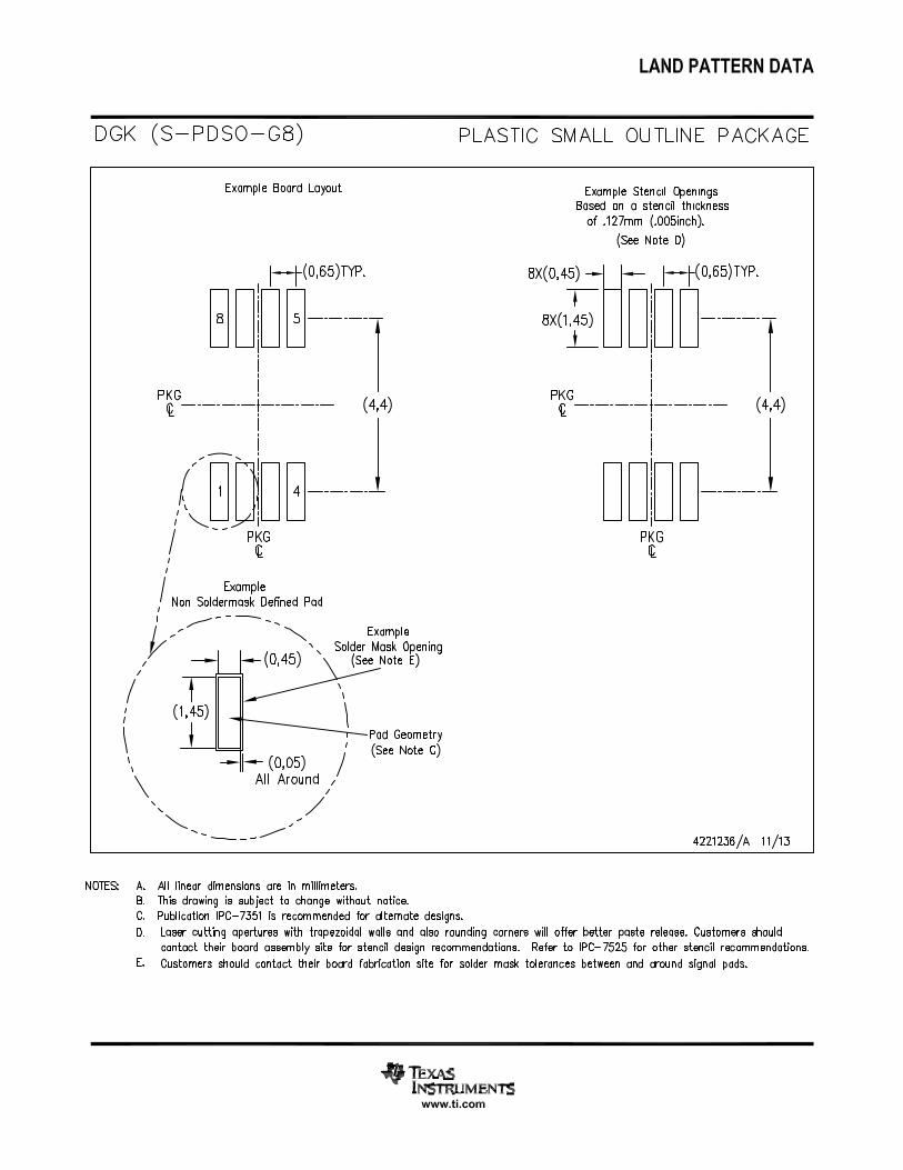
PACKAGE OUTLINE
C
TYP6.66.2
1.2 MAX
6X 0.65
8X 0.300.19
2X1.95
0.150.05
(0.15) TYP
0 - 8
0.25GAGE PLANE
0.750.50
A
NOTE 3
3.12.9
BNOTE 4
4.54.3
4221848/A 02/2015
TSSOP - 1.2 mm max heightPW0008ASMALL OUTLINE PACKAGE
NOTES: 1. All linear dimensions are in millimeters. Any dimensions in parenthesis are for reference only. Dimensioning and tolerancing per ASME Y14.5M. 2. This drawing is subject to change without notice. 3. This dimension does not include mold flash, protrusions, or gate burrs. Mold flash, protrusions, or gate burrs shall not exceed 0.15 mm per side. 4. This dimension does not include interlead flash. Interlead flash shall not exceed 0.25 mm per side.5. Reference JEDEC registration MO-153, variation AA.
18
0.1 C A B
54
PIN 1 IDAREA
SEATING PLANE
0.1 C
SEE DETAIL A
DETAIL ATYPICAL
SCALE 2.800
www.ti.com
EXAMPLE BOARD LAYOUT
(5.8)
0.05 MAXALL AROUND
0.05 MINALL AROUND
8X (1.5)8X (0.45)
6X (0.65)
(R )TYP
0.05
4221848/A 02/2015
TSSOP - 1.2 mm max heightPW0008ASMALL OUTLINE PACKAGE
SYMM
SYMM
LAND PATTERN EXAMPLESCALE:10X
1
45
8
NOTES: (continued) 6. Publication IPC-7351 may have alternate designs. 7. Solder mask tolerances between and around signal pads can vary based on board fabrication site.
METALSOLDER MASKOPENING
NON SOLDER MASKDEFINED
SOLDER MASK DETAILSNOT TO SCALE
SOLDER MASKOPENING
METAL UNDERSOLDER MASK
SOLDER MASKDEFINED
www.ti.com
EXAMPLE STENCIL DESIGN
(5.8)
6X (0.65)
8X (0.45)8X (1.5)
(R ) TYP0.05
4221848/A 02/2015
TSSOP - 1.2 mm max heightPW0008ASMALL OUTLINE PACKAGE
NOTES: (continued) 8. Laser cutting apertures with trapezoidal walls and rounded corners may offer better paste release. IPC-7525 may have alternate design recommendations. 9. Board assembly site may have different recommendations for stencil design.
SYMM
SYMM
1
45
8
SOLDER PASTE EXAMPLEBASED ON 0.125 mm THICK STENCIL
SCALE:10X

IMPORTANT NOTICE
Texas Instruments Incorporated (TI) reserves the right to make corrections, enhancements, improvements and other changes to itssemiconductor products and services per JESD46, latest issue, and to discontinue any product or service per JESD48, latest issue. Buyersshould obtain the latest relevant information before placing orders and should verify that such information is current and complete.TI’s published terms of sale for semiconductor products (http://www.ti.com/sc/docs/stdterms.htm) apply to the sale of packaged integratedcircuit products that TI has qualified and released to market. Additional terms may apply to the use or sale of other types of TI products andservices.Reproduction of significant portions of TI information in TI data sheets is permissible only if reproduction is without alteration and isaccompanied by all associated warranties, conditions, limitations, and notices. TI is not responsible or liable for such reproduceddocumentation. Information of third parties may be subject to additional restrictions. Resale of TI products or services with statementsdifferent from or beyond the parameters stated by TI for that product or service voids all express and any implied warranties for theassociated TI product or service and is an unfair and deceptive business practice. TI is not responsible or liable for any such statements.Buyers and others who are developing systems that incorporate TI products (collectively, “Designers”) understand and agree that Designersremain responsible for using their independent analysis, evaluation and judgment in designing their applications and that Designers havefull and exclusive responsibility to assure the safety of Designers' applications and compliance of their applications (and of all TI productsused in or for Designers’ applications) with all applicable regulations, laws and other applicable requirements. Designer represents that, withrespect to their applications, Designer has all the necessary expertise to create and implement safeguards that (1) anticipate dangerousconsequences of failures, (2) monitor failures and their consequences, and (3) lessen the likelihood of failures that might cause harm andtake appropriate actions. Designer agrees that prior to using or distributing any applications that include TI products, Designer willthoroughly test such applications and the functionality of such TI products as used in such applications.TI’s provision of technical, application or other design advice, quality characterization, reliability data or other services or information,including, but not limited to, reference designs and materials relating to evaluation modules, (collectively, “TI Resources”) are intended toassist designers who are developing applications that incorporate TI products; by downloading, accessing or using TI Resources in anyway, Designer (individually or, if Designer is acting on behalf of a company, Designer’s company) agrees to use any particular TI Resourcesolely for this purpose and subject to the terms of this Notice.TI’s provision of TI Resources does not expand or otherwise alter TI’s applicable published warranties or warranty disclaimers for TIproducts, and no additional obligations or liabilities arise from TI providing such TI Resources. TI reserves the right to make corrections,enhancements, improvements and other changes to its TI Resources. TI has not conducted any testing other than that specificallydescribed in the published documentation for a particular TI Resource.Designer is authorized to use, copy and modify any individual TI Resource only in connection with the development of applications thatinclude the TI product(s) identified in such TI Resource. NO OTHER LICENSE, EXPRESS OR IMPLIED, BY ESTOPPEL OR OTHERWISETO ANY OTHER TI INTELLECTUAL PROPERTY RIGHT, AND NO LICENSE TO ANY TECHNOLOGY OR INTELLECTUAL PROPERTYRIGHT OF TI OR ANY THIRD PARTY IS GRANTED HEREIN, including but not limited to any patent right, copyright, mask work right, orother intellectual property right relating to any combination, machine, or process in which TI products or services are used. Informationregarding or referencing third-party products or services does not constitute a license to use such products or services, or a warranty orendorsement thereof. Use of TI Resources may require a license from a third party under the patents or other intellectual property of thethird party, or a license from TI under the patents or other intellectual property of TI.TI RESOURCES ARE PROVIDED “AS IS” AND WITH ALL FAULTS. TI DISCLAIMS ALL OTHER WARRANTIES ORREPRESENTATIONS, EXPRESS OR IMPLIED, REGARDING RESOURCES OR USE THEREOF, INCLUDING BUT NOT LIMITED TOACCURACY OR COMPLETENESS, TITLE, ANY EPIDEMIC FAILURE WARRANTY AND ANY IMPLIED WARRANTIES OFMERCHANTABILITY, FITNESS FOR A PARTICULAR PURPOSE, AND NON-INFRINGEMENT OF ANY THIRD PARTY INTELLECTUALPROPERTY RIGHTS. TI SHALL NOT BE LIABLE FOR AND SHALL NOT DEFEND OR INDEMNIFY DESIGNER AGAINST ANY CLAIM,INCLUDING BUT NOT LIMITED TO ANY INFRINGEMENT CLAIM THAT RELATES TO OR IS BASED ON ANY COMBINATION OFPRODUCTS EVEN IF DESCRIBED IN TI RESOURCES OR OTHERWISE. IN NO EVENT SHALL TI BE LIABLE FOR ANY ACTUAL,DIRECT, SPECIAL, COLLATERAL, INDIRECT, PUNITIVE, INCIDENTAL, CONSEQUENTIAL OR EXEMPLARY DAMAGES INCONNECTION WITH OR ARISING OUT OF TI RESOURCES OR USE THEREOF, AND REGARDLESS OF WHETHER TI HAS BEENADVISED OF THE POSSIBILITY OF SUCH DAMAGES.Unless TI has explicitly designated an individual product as meeting the requirements of a particular industry standard (e.g., ISO/TS 16949and ISO 26262), TI is not responsible for any failure to meet such industry standard requirements.Where TI specifically promotes products as facilitating functional safety or as compliant with industry functional safety standards, suchproducts are intended to help enable customers to design and create their own applications that meet applicable functional safety standardsand requirements. Using products in an application does not by itself establish any safety features in the application. Designers mustensure compliance with safety-related requirements and standards applicable to their applications. Designer may not use any TI products inlife-critical medical equipment unless authorized officers of the parties have executed a special contract specifically governing such use.Life-critical medical equipment is medical equipment where failure of such equipment would cause serious bodily injury or death (e.g., lifesupport, pacemakers, defibrillators, heart pumps, neurostimulators, and implantables). Such equipment includes, without limitation, allmedical devices identified by the U.S. Food and Drug Administration as Class III devices and equivalent classifications outside the U.S.TI may expressly designate certain products as completing a particular qualification (e.g., Q100, Military Grade, or Enhanced Product).Designers agree that it has the necessary expertise to select the product with the appropriate qualification designation for their applicationsand that proper product selection is at Designers’ own risk. Designers are solely responsible for compliance with all legal and regulatoryrequirements in connection with such selection.Designer will fully indemnify TI and its representatives against any damages, costs, losses, and/or liabilities arising out of Designer’s non-compliance with the terms and provisions of this Notice.
Mailing Address: Texas Instruments, Post Office Box 655303, Dallas, Texas 75265Copyright © 2018, Texas Instruments Incorporated


