LMP91051 Configurable AFE for NDIR Sensing Applications ... · LMP91051 SNAS581B – MARCH 2012–...
26
LMP91051 www.ti.com SNAS581B – MARCH 2012 – REVISED MAY 2013 LMP91051 Configurable AFE for Nondispersive Infrared (NDIR) Sensing Applications Check for Samples: LMP91051 1FEATURES DESCRIPTION 2• Dual Channel Input The LMP91051 is a dual channel programmable • Programmable Gain Amplifier integrated Sensor Analog Front End (AFE) optimized • “Dark Signal” Offset Cancellation for thermopile sensors, as typically used in NDIR applications. It provides a complete signal path • Supports External Filtering solution between a sensor and microcontroller that • Common Mode Generator and 8 Bit DAC generates an output voltage proportional to the • Package 14 Pin TSSOP thermopile voltage. The LMP91051’s programmability enables it to support multiple thermopile sensors with APPLICATIONS a single design as opposed to the multiple discrete solutions. • NDIR Sensing The LMP91051 features a programmable gain • Demand Control Ventilation amplifier (PGA), “dark phase” offset cancellation, and • Building Monitoring an adjustable common mode generator (1.15V or • CO2 Cabin Control — Automotive 2.59V) which increases output dynamic range. The PGA offers a low gain range of 167V/V to 1335V/V • Alcohol Detection — Automotive plus a high gain range of 1002V/V to 7986V/V which • Industrial Safety and Security enables the user to utilize thermopiles with different • GHG & Freons Detection Platforms sensitivities. The PGA is highlighted by low gain drift (20 ppm/°C), output offset drift (230 mV/°C at KEY SPECIFICATIONS G = 1002 V/V), phase delay drift (300 ns) and noise specifications (0.1 μVRMS 0.1 to 10Hz) . The offset • Programmable Gain … 167V/V to 7986V/V cancellation circuitry compensates for the “dark • Low Noise (0.1 to 10 Hz) … 0.1μVRMS signal” by adding an equal and opposite offset to the • Gain Drift … 20 ppm/°C (typ) input of the second stage, thus removing the original offset from the output signal. This offset cancellation • Phase Delay Drift … 300 ns (typ) circuitry allows optimized usage of the ADC full scale • Power supply voltage range … 2.7V to 5.5V and relaxes ADC resolution requirements. The LMP91051 allows extra signal filtering (high pass, low pass or band pass) through dedicated pins A0 and A1, in order to remove out of band noise. The user can program through the on board SPI interface. Available in a small form factor 14 pin TSSOP package, the LMP91051 operates from –40 to +105°C. 1 Please be aware that an important notice concerning availability, standard warranty, and use in critical applications of Texas Instruments semiconductor products and disclaimers thereto appears at the end of this data sheet. 2All trademarks are the property of their respective owners. PRODUCTION DATA information is current as of publication date. Copyright © 2012–2013, Texas Instruments Incorporated Products conform to specifications per the terms of the Texas Instruments standard warranty. Production processing does not necessarily include testing of all parameters.
Transcript of LMP91051 Configurable AFE for NDIR Sensing Applications ... · LMP91051 SNAS581B – MARCH 2012–...

LMP91051
www.ti.com SNAS581B –MARCH 2012–REVISED MAY 2013
LMP91051 Configurable AFE for Nondispersive Infrared (NDIR) Sensing ApplicationsCheck for Samples: LMP91051
1FEATURESDESCRIPTION
2• Dual Channel InputThe LMP91051 is a dual channel programmable• Programmable Gain Amplifierintegrated Sensor Analog Front End (AFE) optimized
• “Dark Signal” Offset Cancellation for thermopile sensors, as typically used in NDIRapplications. It provides a complete signal path• Supports External Filteringsolution between a sensor and microcontroller that• Common Mode Generator and 8 Bit DACgenerates an output voltage proportional to the
• Package 14 Pin TSSOP thermopile voltage. The LMP91051’s programmabilityenables it to support multiple thermopile sensors with
APPLICATIONS a single design as opposed to the multiple discretesolutions.• NDIR SensingThe LMP91051 features a programmable gain• Demand Control Ventilationamplifier (PGA), “dark phase” offset cancellation, and• Building Monitoringan adjustable common mode generator (1.15V or
• CO2 Cabin Control — Automotive 2.59V) which increases output dynamic range. ThePGA offers a low gain range of 167V/V to 1335V/V• Alcohol Detection — Automotiveplus a high gain range of 1002V/V to 7986V/V which• Industrial Safety and Securityenables the user to utilize thermopiles with different
• GHG & Freons Detection Platforms sensitivities. The PGA is highlighted by low gain drift(20 ppm/°C), output offset drift (230 mV/°C at
KEY SPECIFICATIONS G = 1002 V/V), phase delay drift (300 ns) and noisespecifications (0.1 µVRMS 0.1 to 10Hz) . The offset• Programmable Gain … 167V/V to 7986V/Vcancellation circuitry compensates for the “dark
• Low Noise (0.1 to 10 Hz) … 0.1µVRMS signal” by adding an equal and opposite offset to the• Gain Drift … 20 ppm/°C (typ) input of the second stage, thus removing the original
offset from the output signal. This offset cancellation• Phase Delay Drift … 300 ns (typ)circuitry allows optimized usage of the ADC full scale
• Power supply voltage range … 2.7V to 5.5V and relaxes ADC resolution requirements.
The LMP91051 allows extra signal filtering (highpass, low pass or band pass) through dedicated pinsA0 and A1, in order to remove out of band noise. Theuser can program through the on board SPI interface.Available in a small form factor 14 pin TSSOPpackage, the LMP91051 operates from –40 to+105°C.
1
Please be aware that an important notice concerning availability, standard warranty, and use in critical applications ofTexas Instruments semiconductor products and disclaimers thereto appears at the end of this data sheet.
2All trademarks are the property of their respective owners.
PRODUCTION DATA information is current as of publication date. Copyright © 2012–2013, Texas Instruments IncorporatedProducts conform to specifications per the terms of the TexasInstruments standard warranty. Production processing does notnecessarily include testing of all parameters.

MSP430
AVSS/DVSS
LMP91051
IN2
Active Thermopile
OUT
A0 A1VDD
CMOUT
IN1
VIO
A/D
VIO
DVCC
GND
CSB
SDIO
SCLK
GPIO
CLK
MOSI
VDD
AVCC
VDD
VIOReference Thermopile
OUT
IN2
DAC
VREFCM GEN
G1=250,42 G2=4,8,16,32
VDD
LMP91051
CMOUT
+
- PGA1
+
- PGA2
A0 A1
CMOUT
IN1
SPI
GND
CSB
SCLK
SDIO
VIO
Optional External
Filter
SPI
LMP91051
SNAS581B –MARCH 2012–REVISED MAY 2013 www.ti.com
These devices have limited built-in ESD protection. The leads should be shorted together or the device placed in conductive foamduring storage or handling to prevent electrostatic damage to the MOS gates.
BLOCK DIAGRAM
Configurable AFE for NDIR
TYPICAL APPLICATION
Typical NDIR Sensing Application Circuit
2 Submit Documentation Feedback Copyright © 2012–2013, Texas Instruments Incorporated
Product Folder Links: LMP91051

SVA-30180650
LMP91051
www.ti.com SNAS581B –MARCH 2012–REVISED MAY 2013
CONNECTION DIAGRAM
PIN DESCRIPTIONSPIN
I/O DESCRIPTIONNAME NO.
IN1 1 Analog Input Signal Input
IN2 2 Analog Input Signal Input
CMOUT 3 Analog Output Common Mode Voltage Output
A0 4 Analog Output First Stage Output
A1 5 Analog Input Second Stage Input
GND 6 Power Ground
NC 7 — No Connect
NC 8 — No Connect
OUT 9 Analog Output Signal Output, reference to the same potential as CMOUT
CSB 10 Digital Input Chip Select, active low
SCLK 11 Digital Input Interface Clock
SDIO 12 Digital Input / Output Serial Data Input / Output
VIO 13 Power Digital Input/Output Supply
VDD 14 Power Positive Supply
Copyright © 2012–2013, Texas Instruments Incorporated Submit Documentation Feedback 3
Product Folder Links: LMP91051

LMP91051
SNAS581B –MARCH 2012–REVISED MAY 2013 www.ti.com
ABSOLUTE MAXIMUM RATINGS (1) (2)
over operating free-air temperature range (unless otherwise noted)
MIN MAX UNIT
Human Body Model 1000ESD Tolerance (3) V
Charged Device Model 250
VDD Supply Voltage –0.3 6.0 V
VIO Digital I/O supply –0.3 6.0 V
Voltage at Any Pin ––0.3 VDD + 0.3 V
Input Current at Any Pin 5 mA
Storage Temperature Range 65 150 °C
Junction Temperature (4) 150 °C
For soldering specifications: see product folder at www.national.com andwww.national.com/ms/MS/MS-SOLDERING.pdf
(1) “Absolute Maximum Ratings” indicate limits beyond which damage to the device may occur, including inoperability and degradation ofdevice reliability and/or performance. Functional operation of the device and/or non-degradation at the Absolute Maximum Ratings orother conditions beyond those indicated in the Operating Ratings is not implied. Operating Ratings indicate conditions at which thedevice is functional and the device should not be operated beyond such conditions.
(2) If Military/Aerospace specified devices are required, please contact the Texas Instruments Sales Office/ Distributors for availability andspecifications.
(3) Human Body Model, applicable std. MIL-STD-883, Method 3015.7. Machine Model, applicable std. JESD22-A115-A (ESD MM std. ofJEDEC) Field- Induced Charge-Device Model, applicable std. JESD22-C101-C (ESD FICDM std. of JEDEC).
(4) The maximum power dissipation is a function of TJ(MAX), θJA, and the ambient temperature, TA. The maximum allowable powerdissipation at any ambient temperature is PDMAX = (TJ(MAX) - TA)/ θJA All numbers apply for packages soldered directly onto a PC board.
OPERATING CHARACTERISTICS (1)
over operating free-air temperature range (unless otherwise noted)
PARAMETER TEST CONDITIONS MIN TYP MAX UNIT
Supply Voltage 2.7 5.5 V
Junction Temperature Range (2) –40 105 °C
θJA Package Thermal Resitance Package 14 pin TSSOP 140 °C/W
(1) “Absolute Maximum Ratings” indicate limits beyond which damage to the device may occur, including inoperability and degradation ofdevice reliability and/or performance. Functional operation of the device and/or non-degradation at the Absolute Maximum Ratings orother conditions beyond those indicated in the Operating Ratings is not implied. Operating Ratings indicate conditions at which thedevice is functional and the device should not be operated beyond such conditions.
(2) The maximum power dissipation is a function of TJ(MAX), θJA, and the ambient temperature, TA. The maximum allowable powerdissipation at any ambient temperature is PDMAX = (TJ(MAX) - TA)/ θJA All numbers apply for packages soldered directly onto a PC board.
ELECTRICAL CHARACTERISTICS (1)
The following specifications apply for VDD = 3.3V, VIO = 3.3V, VCM = 1.15V, Bold values for TA = -40°C to +85°C unlessotherwise specified. All other limits apply to TA = TJ = +25°C.
PARAMETER TEST CONDITIONS MIN (2) TYP (3) MAX (2) UNIT
Power Supply
VDD Supply Voltage 2.7 3.3 5.5 V
VIO Digital I/O supply 2.7 3.3 5.5 V
IDD Supply Current All analog block ON 3.1 3.6 4.2 mA
Power Down Supply Current All analog block OFF 45 75 121 µA
Digital Supply Current 8 µA
(1) Electrical Table values apply only for factory testing conditions at the temperature indicated. Factory testing conditions result in verylimited self-heating of the device such that TJ = TA. No guarantee of parametric performance is indicated in the electrical tables underconditions of internal self-heating where TJ > TA. Absolute Maximum Ratings indicate junction temperature limits beyond which thedevice may be permanently degraded, either mechanically or electrically.
(2) Limits are 100% production tested at 25°C. Limits over the operating temperature range are guaranteed through correlations usingstatistical quality control (SQC) method.
(3) Typical values represent the most likely parametric norm as determined at the time of characterization. Actual typical values may varyover time and will also depend on the application and configuration. The typical values are not tested and are not guaranteed onshipped production material.
4 Submit Documentation Feedback Copyright © 2012–2013, Texas Instruments Incorporated
Product Folder Links: LMP91051

LMP91051
www.ti.com SNAS581B –MARCH 2012–REVISED MAY 2013
ELECTRICAL CHARACTERISTICS(1) (continued)The following specifications apply for VDD = 3.3V, VIO = 3.3V, VCM = 1.15V, Bold values for TA = -40°C to +85°C unlessotherwise specified. All other limits apply to TA = TJ = +25°C.
PARAMETER TEST CONDITIONS MIN (2) TYP (3) MAX (2) UNIT
Offset Cancellation (Offset DAC)
Resolution 256 steps
LSB All gains 33.8 mV
DNL –1 +2 LSB
Error Output referred offset error, all gains ±100 mV
VDD –Offset adjust Range Output referred, all gains 0.2 V0.2
DAC settling time 480 µs
Programmable Gain Amplifier (PGA) 1st Stage, RL = 10 kΩ, CL = 15 pF
IBIAS Bias Current 5 200 pA
VINMAX Referenced to CMOUT voltage, it refersMax input signal High gain mode ±2 mV_HGM to the maximum voltage at the IN pinbefore clipping; It includes dark voltageVINMAX Max input signal Low gain mode ±12 mVof the thermopile and signal voltage._LGM
VOS Input Offset Voltage –165 µV
G _HGM Gain High gain mode 250 V/V
G_LGM Gain Low gain mode 42 V/V
GE Gain Error Both HGM and LGM 2.5 %
VDD –VOUT Output Voltage Range 0.5 V0.5
1mV input step signal, HGM, VoutPhDly Phase Delay 6 µsmeasured at Vdd/2
Phase Delay variation with 1mV input step signal, HGM, VoutTCPhDly 416 nsTemperature measured at Vdd/2,
SSBW Small Signal Bandwidth Vin = 1mVpp, Gain = 250 V/V 18 kHz
Cin Input Capacitance 100 pF
Programmable Gain Amplifier (PGA) 2nd Stage, RS = 1kΩ, CL = 1µF
VINMAX Max input signal GAIN = 4 V/V 1.65 V
VINMIN Min input signal 0.82 V
G Gain Programmable in 4 steps 4 32 V/V
GE Gain Error Any gain 2.5 %
VDD –VOUT Output Voltage Range 0.2 V0.2
100mV input sine 35kHz signal, Gain =PhDly Phase Delay 8, VOUT measureed at 1.65V, RL = 10 1 µs
kΩPhase Delay variation with 250mV input step signal, Gain = 8, VoutTCPhDly 84 nsTemperature measured at Vdd/2
SSBW Small Signal Bandwidth Gain = 32 V/V 360 kHz
Cin Input Capacitance 5 pF
CLOAD, OUT Pin Load Capacitance Series RC 1 µFOUT
RLOAD, OUT Pin Load Resistance Series RC 1 kΩOUT
Copyright © 2012–2013, Texas Instruments Incorporated Submit Documentation Feedback 5
Product Folder Links: LMP91051

LMP91051
SNAS581B –MARCH 2012–REVISED MAY 2013 www.ti.com
ELECTRICAL CHARACTERISTICS(1) (continued)The following specifications apply for VDD = 3.3V, VIO = 3.3V, VCM = 1.15V, Bold values for TA = -40°C to +85°C unlessotherwise specified. All other limits apply to TA = TJ = +25°C.
PARAMETER TEST CONDITIONS MIN (2) TYP (3) MAX (2) UNIT
Combined Amplifier Chain Specification
Combination of both current and voltageen Input-Referred Noise Density noise, with a 86kΩ source impedance at 30 nV√Hz
5Hz, Gain = 7986
Combination of both current and voltageInput-Referred Integrated Noise noise, with a 86kΩ source impedance 0.1 0.12 (4) µVrms
0.1Hz to 10Hz, Gain = 7986
PGA1 GAIN = 42, PGA2 GAIN = 4 167
PGA1 GAIN = 42, PGA2 GAIN = 8 335
PGA1 GAIN = 42, PGA2 GAIN = 16 669
PGA1 GAIN = 42, PGA2 GAIN = 3 1335G Gain V/V
2 PGA1 GAIN = 250, PGA2 GAIN = 4 1002
PGA1 GAIN = 250, PGA2 GAIN = 8 2004
PGA1 GAIN = 250, PGA2 GAIN = 16 4003
PGA1 GAIN = 250, PGA2 GAIN = 32 7986
GE Gain Error Any gain 5 %
Gain = 167 V/V, 335 V/V, 669 V/V, 1335 6V/VTCCGE Gain Temp Coefficient (5) ppm/°C
Gain = 1002 V/V, 2004 V/V, 4003 V/V, 207986V/V
PSRR Power Supply Rejection Ratio DC, 3.0V to 3.6V supply, gain = 1002V/V 90 110 dB
1mV input step signal, Gain = 1002,PhDly Phase Delay 9 µsVout measured at Vdd/2
Phase Delay variation with 1mV input step signal, Gain=1002, VoutTCPhDly 300 nsTemperature (6) measured at Vdd/2
Gain = 167 V/V 70
Gain = 335 V/V 100
Gain = 669 V/V 160
Gain = 1335 V/V 290Output Offset Voltage TemperatureTCVOS µV/°CDrift (5)Gain = 1002 V/V 230
Gain = 2004 V/V 420
Gain = 4003 V/V 800
Gain = 7986V/V 1550
Common Mode Generator
VDD = 3.3V 1.15 VVCM Common Mode Voltage
VDD = 5V 2.59
VCM accuracy 2 %
CLOAD CMOut Load Capacitance 10 nF
(4) Guaranteed by design and characterization. Not tested on shipped production material.(5) TCCGE and TCVOS are calculated by taking the largest slope between –40°C and 25°C linear interpolation and 25°C and 85°C linear
interpolation.(6) TCPhDly is largest change in phase delay between –40°C and 25°C measurements and 25°C and 85°C measurements.
6 Submit Documentation Feedback Copyright © 2012–2013, Texas Instruments Incorporated
Product Folder Links: LMP91051

LMP91051
www.ti.com SNAS581B –MARCH 2012–REVISED MAY 2013
SPI INTERFACE (1)
The following specifications apply for VDD = 3.3V, VIO = 3.3V, VCM = 1.15V, CL = 15pF, Bold values for TA = –40°C to+85°C unless otherwise specified. All other limits apply to TA = TJ = +25°C.
PARAMETER TEST CONDITIONS MIN (2) TYP (3) MAX (2) UNIT
VIH Logic Input High 0.7 × VDD V
VIL Logic Input Low 0.8 V
VOH Logic Output High 2.6 V
VOL Logic Output Low 0.4 V
–100 100IIH/IIL Input Digital Leakage Current nA–200 200
(1) Electrical Table values apply only for factory testing conditions at the temperature indicated. Factory testing conditions result in verylimited self-heating of the device such that TJ = TA. No guarantee of parametric performance is indicated in the electrical tables underconditions of internal self-heating where TJ > TA. Absolute Maximum Ratings indicate junction temperature limits beyond which thedevice may be permanently degraded, either mechanically or electrically.
(2) Limits are 100% production tested at 25°C. Limits over the operating temperature range are guaranteed through correlations usingstatistical quality control (SQC) method.
(3) Typical values represent the most likely parametric norm as determined at the time of characterization. Actual typical values may varyover time and will also depend on the application and configuration. The typical values are not tested and are not guaranteed onshipped production material.
TIMING CHARACTERISTICS (1)
The following specifications apply for VDD = 3.3V, VIO = 3.3V, VCM = 1.15V, CL = 15pF, Bold values for TA = –40°C to+85°C unless otherwise specified. All other limits apply to TA = TJ = +25°C.
PARAMETER TEST CONDITIONS MIN (2) TYP (3) MAX (2) UNIT
tWU Wake up time 1 ms
fSCLK Serial Clock Frequency 10 MHz
tPH SCLK Pulse Width High 0.4/fSCLK ns
tPL SCLK Pulse Width Low 0.4/fSCLK ns
tCSS CSB Setup Time 10 ns
tCSH CSB Hold Time 10 ns
SDI Setup Time prior to rise edge of 10tSU nsSCLK
SDI Hold Time prior to rise edge of 10tSH nsSCLK
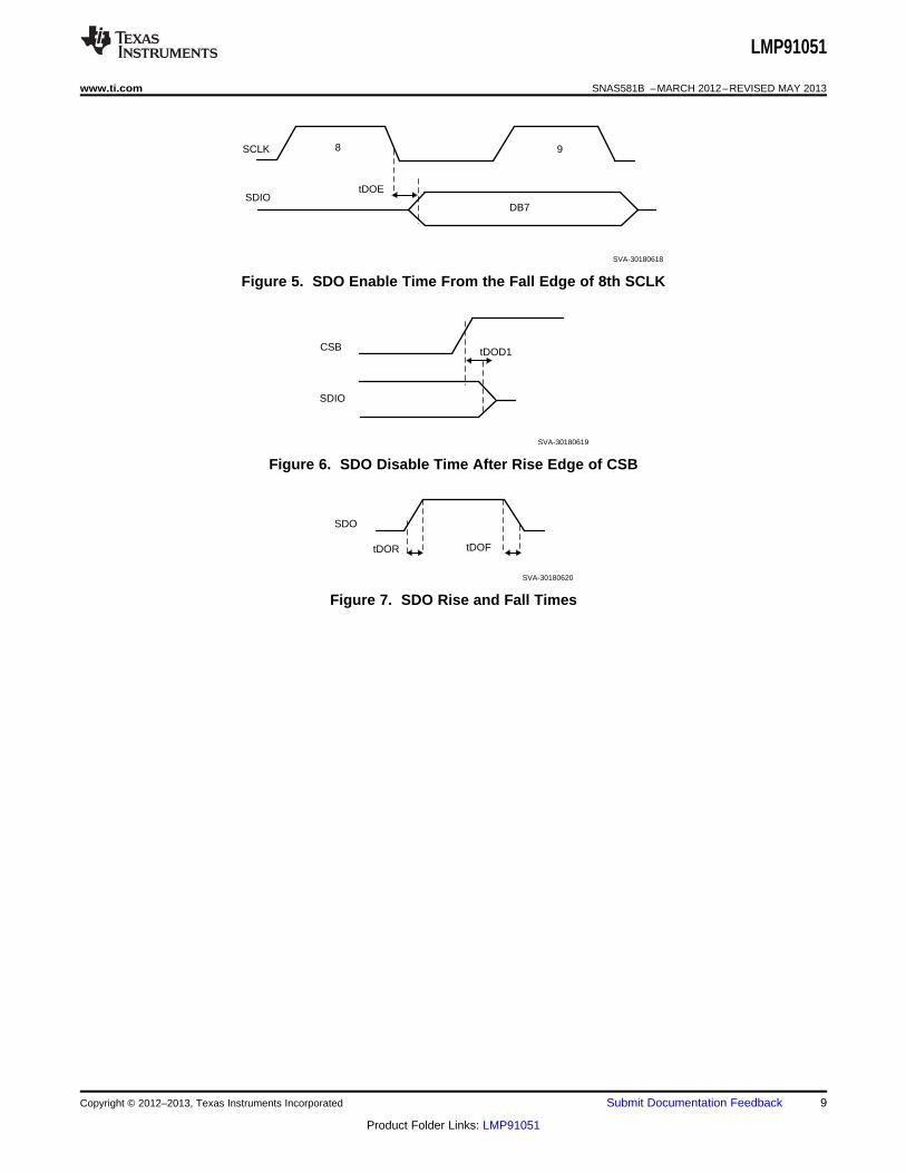
SDO Disable Time after rise edge oftDOD1 45 nsCSB
SDO Disable Time after 16th risetDOD2 45 nsedge of SCLK
SDO Enable Time from the fall edgetDOE 35 nsof 8th SCLK
SDO Access Time after the fall edgetDOA 35 nsof SCLK
SDO hold time after the fall edge of 5tDOH nsSCLK
tDOR SDO Rise time 5 ns
tDOF SDO Fall time 5 ns
(1) Electrical Table values apply only for factory testing conditions at the temperature indicated. Factory testing conditions result in verylimited self-heating of the device such that TJ = TA. No guarantee of parametric performance is indicated in the electrical tables underconditions of internal self-heating where TJ > TA. Absolute Maximum Ratings indicate junction temperature limits beyond which thedevice may be permanently degraded, either mechanically or electrically.
(2) Limits are 100% production tested at 25°C. Limits over the operating temperature range are guaranteed through correlations usingstatistical quality control (SQC) method.
(3) Typical values represent the most likely parametric norm as determined at the time of characterization. Actual typical values may varyover time and will also depend on the application and configuration. The typical values are not tested and are not guaranteed onshipped production material.
Copyright © 2012–2013, Texas Instruments Incorporated Submit Documentation Feedback 7
Product Folder Links: LMP91051

SVA-30180616
SCLK
SDIO DB
tDOH
tDOA
DB
SVA-30180617
DB0
tDOD2
SCLK
SDIO
Valid Data
tHtSU
tPHtPL
SDI
16th clock
SCLK
Valid Data
SVA-30180613
SVA-30180612
LMP91051
SNAS581B –MARCH 2012–REVISED MAY 2013 www.ti.com
Timing Diagrams
Figure 1. SPI Timing Diagram
Figure 2. SPI Set-up Hold Time
Figure 3. SDO Disable Time After 16th Rise Edge of SCLK
Figure 4. SDO Access Time (tDOA) and SDO Hold Time (tDOH) After the Fall Edge of SCLK
8 Submit Documentation Feedback Copyright © 2012–2013, Texas Instruments Incorporated
Product Folder Links: LMP91051
SVA-30180620
tDOFtDOR
SDO
SVA-30180619
tDOD1
SDIO
CSB
SVA-30180618
tDOE
8
DB7
9
SDIO
SCLK
LMP91051
www.ti.com SNAS581B –MARCH 2012–REVISED MAY 2013
Figure 5. SDO Enable Time From the Fall Edge of 8th SCLK
Figure 6. SDO Disable Time After Rise Edge of CSB
Figure 7. SDO Rise and Fall Times
Copyright © 2012–2013, Texas Instruments Incorporated Submit Documentation Feedback 9
Product Folder Links: LMP91051

-50 -25 0 25 50 75 100
2008
2009
2010
2011
2012
2013
2014
GA
IN (
V/V
)
TEMPERATURE (°C)
SVA-30180626
-50 -25 0 25 50 75 100
8.6
8.7
8.8
8.9
9.0
9.1
9.2
9.3
PH
AS
E D
ELA
Y (�
s)
TEMPERATURE (°C)
SVA-30180622
-50 -25 0 25 50 75 100671.7
671.8
671.9
672.0
672.1
672.2
672.3
672.4
672.5
GA
IN (
V/V
)
TEMPERATURE (°C)
SVA-30180623
-50 -25 0 25 50 75 100
1008
1009
1010
1011
GA
IN (
V/V
)
TEMPERATURE (°C)
SVA-30180627
-50 -25 0 25 50 75 100335.4
335.5
335.6
335.7
335.8
335.9
336.0
GA
IN (
V/V
)
TEMPERATURE (°C)
SVA-30180624
-50 -25 0 25 50 75 100
167.8
167.9
168.0
168.1
168.2
168.3
168.4
GA
IN (
V/V
)
TEMPERATURE (°C)
SVA-30180625
LMP91051
SNAS581B –MARCH 2012–REVISED MAY 2013 www.ti.com
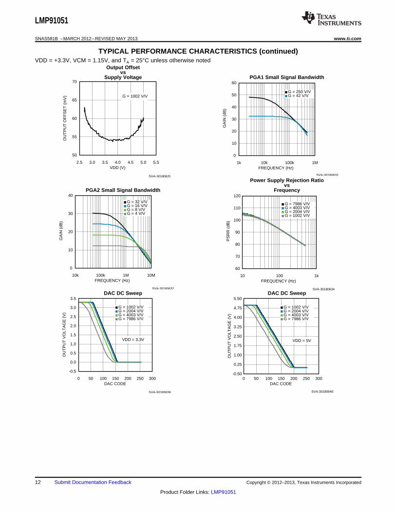
TYPICAL PERFORMANCE CHARACTERISTICSVDD = +3.3V, VCM = 1.15V, and TA = 25°C unless otherwise noted
Gain = 167 V/V Gain = 335 V/Vvs vs
Temperature Temperature
Gain = 669 V/V Gain = 1002 V/Vvs vs
Temperature Temperature
Gain = 2004 V/V Phase Delayvs vs
Temperature Temperature
10 Submit Documentation Feedback Copyright © 2012–2013, Texas Instruments Incorporated
Product Folder Links: LMP91051

2.5 3.0 3.5 4.0 4.5 5.0 5.5
60
70
80
90
100
110
120
IDD
(�
A)
VDD (V)
SVA-30180630
2.5 3.0 3.5 4.0 4.5 5.0 5.5
0.0
0.5
1.0
1.5
2.0
2.5
3.0
3.5
4.0
4.5
IDD
(m
A)
VDD (V)
PGA ALL ONPGA2 ONPGA1 ON
SVA-30180631
-50 -25 0 25 50 75 100
-5
-4
-3
-2
-1
0
IBIA
S (
pA)
TEMPERATURE (°C)
SVA-30180643
-50 -25 0 25 50 75 100
0
1
2
3
4
5
IDD
(m
A)
TEMPERATURE (°C)
G = 1002 V/V
SVA-30180642
-50 -25 0 25 50 75 100
0
10
20
30
40
50
60
70
80
90
100
OU
TP
UT
OF
FS
ET
(m
V)
TEMPERATURE (°C)
G = 1002 V/V
SVA-30180628
-50 -25 0 25 50 75 1001.150
1.152
1.154
1.156
1.158
1.160
CO
MM
ON
MO
DE
VO
LTA
GE
(V
)
TEMPERATURE (°C)
SVA-301806100
LMP91051
www.ti.com SNAS581B –MARCH 2012–REVISED MAY 2013
TYPICAL PERFORMANCE CHARACTERISTICS (continued)VDD = +3.3V, VCM = 1.15V, and TA = 25°C unless otherwise noted
Output Offset Common Mode Voltagevs vs
Temperature Temperature
Input Bias Current Supply Currentvs vs
Temperature Temperature
Supply Current Power Down Supply Currentvs vs
Supply Voltage Supply Voltage
Copyright © 2012–2013, Texas Instruments Incorporated Submit Documentation Feedback 11
Product Folder Links: LMP91051
0 50 100 150 200 250 300
-0.5
0.0
0.5
1.0
1.5
2.0
2.5
3.0
3.5
OU
TP
UT
VO
LTA
GE
(V
)
DAC CODE
VDD = 3.3V
G = 1002 V/VG = 2004 V/VG = 4003 V/VG = 7986 V/V
SVA-30180639
0 50 100 150 200 250 300-0.50
0.25
1.00
1.75
2.50
3.25
4.00
4.75
5.50
OU
TP
UT
VO
LTA
GE
(V
)
DAC CODE
VDD = 5V
G = 1002 V/VG = 2004 V/VG = 4003 V/VG = 7986 V/V
SVA-30180640
10 100 1k
60
70
80
90
100
110
120
PS
RR
(dB
)
FREQUENCY (Hz)
G = 7986 V/VG = 4003 V/VG = 2004 V/VG = 1002 V/V
SVA-30180634
10k 100k 1M 10M
0
10
20
30
40
GA
IN (
dB)
FREQUENCY (Hz)
G = 32 V/VG = 16 V/VG = 8 V/VG = 4 V/V
SVA-30180632
2.5 3.0 3.5 4.0 4.5 5.0 5.5
50
55
60
65
70
OU
TP
UT
OF
FS
ET
(m
V)
VDD (V)
G = 1002 V/V
SVA-30180629
1k 10k 100k 1M
0
10
20
30
40
50
60
GA
IN (
dB)
FREQUENCY (Hz)
G = 250 V/VG = 42 V/V
SVA-30180633
LMP91051
SNAS581B –MARCH 2012–REVISED MAY 2013 www.ti.com
TYPICAL PERFORMANCE CHARACTERISTICS (continued)VDD = +3.3V, VCM = 1.15V, and TA = 25°C unless otherwise noted
Output Offsetvs
Supply Voltage PGA1 Small Signal Bandwidth
Power Supply Rejection Ratiovs
PGA2 Small Signal Bandwidth Frequency
DAC DC Sweep DAC DC Sweep
12 Submit Documentation Feedback Copyright © 2012–2013, Texas Instruments Incorporated
Product Folder Links: LMP91051
10 PF
160 k:
160 k:
6.8 nF
CMOUT
A0 A1
SVA-30180607
LMP91051
www.ti.com SNAS581B –MARCH 2012–REVISED MAY 2013
FUNCTIONAL DESCRIPTION
PROGRAMMABLE GAIN AMPLIFIER
The LMP91051 offers two programmable gain modes (low/high) with four programmable gain settings each. Thepurpose of the gain mode is to enable thermopiles with larger dark voltage levels. All gain settings are accessiblethrough bits GAIN1 and GAIN2 [1:0]. The low gain mode has a range of 167 V/V to 1335 V/V while the high gainmode has a range of 1002 V/V to 7986 V/V. The PGA is referenced to the internally generated VCM. Inputsignal, referenced to this VCM voltage, should be within +/-2mV (see VINMAX_HGM specification) in high gainmode. In the low gain mode the first stage will provide a gain of 42 V/V instead of 250 V/V, thus allowing a largermaximum input signal up to +/-12mV (VINMAX_LGM).
Table 1. Gain Modes
BIT SYMBOL GAIN
0: 250 (default)GAIN1 1: 42
00: 4 (default)01: 8GAIN2 [1:0] 10: 1611: 32
EXTERNAL FILTER
The LMP91051 offers two different measurement modes selectable through EXT_FILT bit. EXT_FILT bit ispresent in the Device configuration register and is programmable through SPI.
Table 2. Measurement Modes
BIT SYMBOL MEASUREMENT MODE
0: The signal from the thermopile is being processed by the internal PGAs,EXT_FILT without additional external decoupling or filtering (default).
1: The signal from the thermopile is being processed by the first internal PGA andfed to the A0 pin. An external low pass, high pass or band pass filter can beconnected through pins A0, A1.
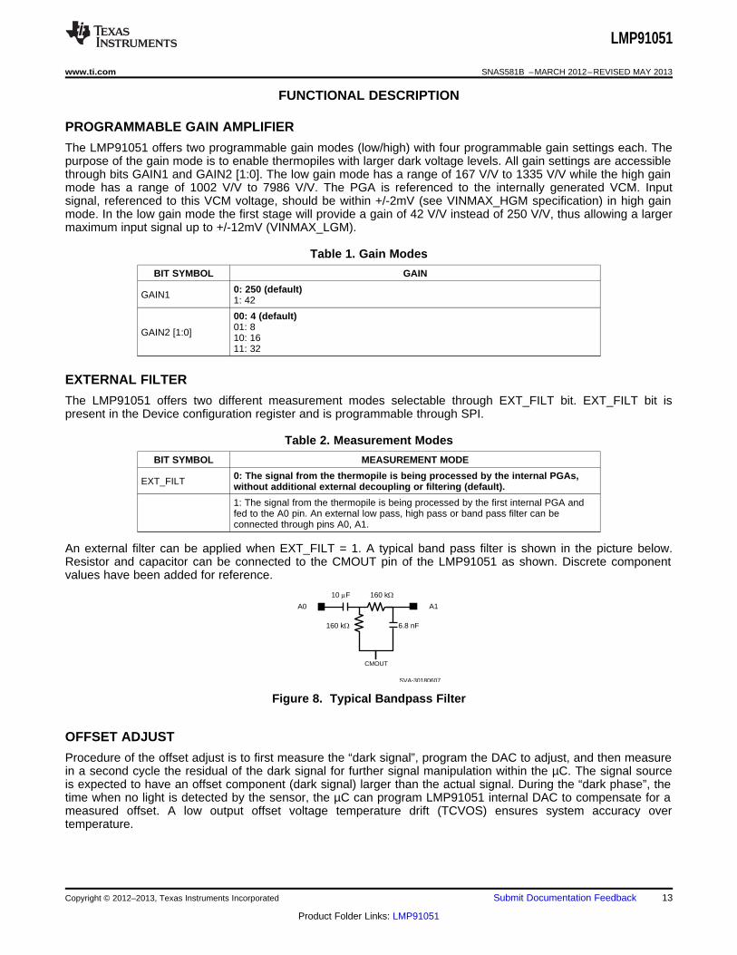
An external filter can be applied when EXT_FILT = 1. A typical band pass filter is shown in the picture below.Resistor and capacitor can be connected to the CMOUT pin of the LMP91051 as shown. Discrete componentvalues have been added for reference.
Figure 8. Typical Bandpass Filter
OFFSET ADJUST
Procedure of the offset adjust is to first measure the “dark signal”, program the DAC to adjust, and then measurein a second cycle the residual of the dark signal for further signal manipulation within the µC. The signal sourceis expected to have an offset component (dark signal) larger than the actual signal. During the “dark phase”, thetime when no light is detected by the sensor, the µC can program LMP91051 internal DAC to compensate for ameasured offset. A low output offset voltage temperature drift (TCVOS) ensures system accuracy overtemperature.
Copyright © 2012–2013, Texas Instruments Incorporated Submit Documentation Feedback 13
Product Folder Links: LMP91051
c7 c6 c5 c4 c3 c2 c1 c0 d7 d6 d5 d4 d3 d2 d1 d0
CSB
SCK
COMMAND FIELD DATA FIELD
1 2 3 4 5 6 7 8 9 10 11 12 13 14 15 16
LSBMSB
Reserved to 0 Address (4 bits) Write Data (8-bits)Wb=0
SVA-30180609
LMP91051
SNAS581B –MARCH 2012–REVISED MAY 2013 www.ti.com
COMMON MODE GENERATION
As the sensor’s offset is bipolar, there is a need to supply a VCM to the sensor. This can be programmed as1.15V or 2.59V (approximately mid rail of 3.3V or 5V supply). It is not recommended to use 2.59V VCM with 3.3Vsupply.
SPI INTERFACE
An SPI interface is available in order to program the device parameters like PGA gain of two stages, enablingexternal filter, enabling power for PGAs, offset adjust and common mode (VCM) voltage.
Interface Pins
The Serial Interface consists of SDIO (Serial Data Input / Output), SCLK (Serial Interface Clock) and CSB (ChipSelect Bar). The serial interface is write-only by default. Read operations are supported after enabling the SDIOmode by programming the SDIO_MODE_EN register. This is discussed in detail later in the document.
CSB
Chip Select is a active-low signal. CSB needs to be asserted throughout a transaction. That is, CSB should notpulse between the Instruction Byte and the Data Byte of a single transaction.
Note that CSB de-assertion always terminates an on-going transaction, if it is not already complete. Likewise,CSB assertion will always bring the device into a state, ready for next transaction, regardless of the terminationstatus of a previous transaction.
CSB may be permanently tied low for a 2-wire SPI communication protocol.
SCLK
SCLK can idle High or Low for a write transaction. However, for a READ transaction, SCLK should idle high.SCLK features a Schmitt-triggered input and although it has hysterisis, it is recommened to keep SCLK as cleanas possible to prevent glitches from inadvertently spoiling the SPI frame.
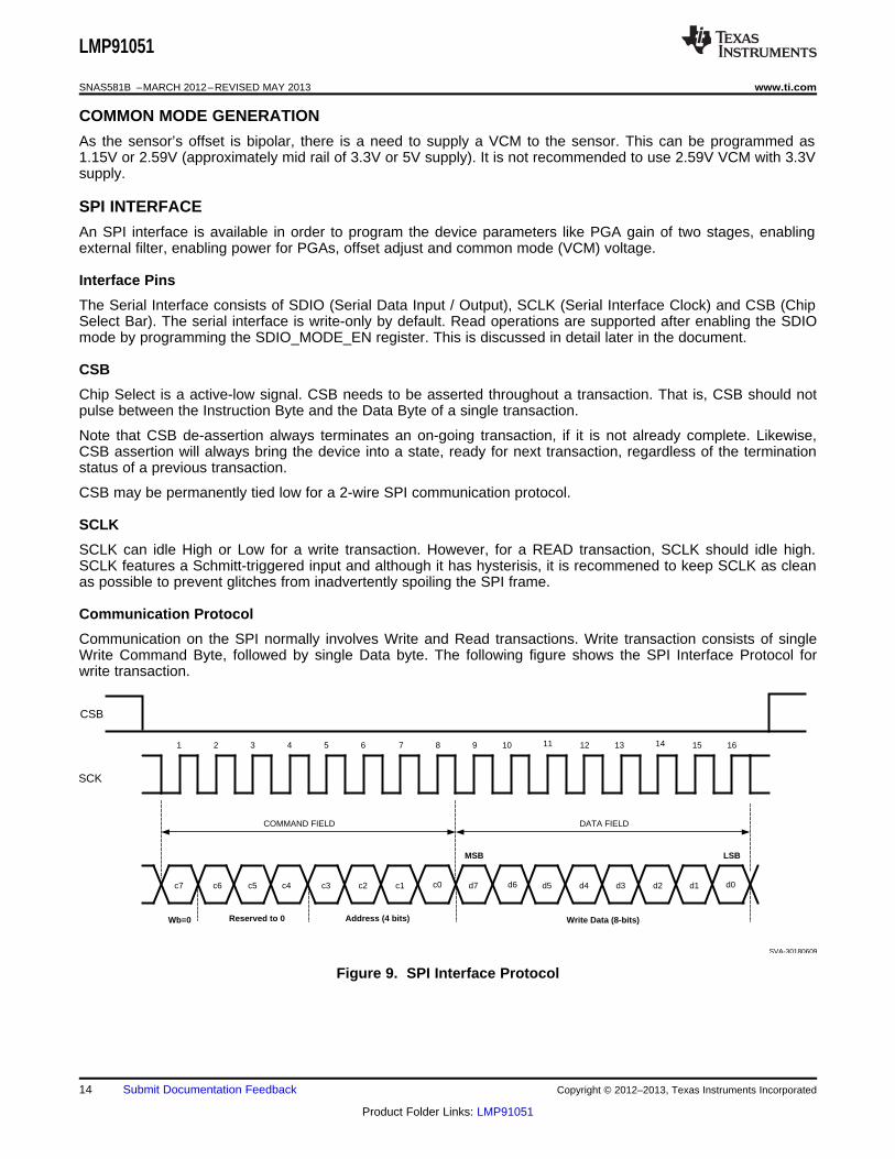
Communication Protocol
Communication on the SPI normally involves Write and Read transactions. Write transaction consists of singleWrite Command Byte, followed by single Data byte. The following figure shows the SPI Interface Protocol forwrite transaction.
Figure 9. SPI Interface Protocol
14 Submit Documentation Feedback Copyright © 2012–2013, Texas Instruments Incorporated
Product Folder Links: LMP91051
Write cmd(sdio_mode_en reg)
Write data(0xFE first
byte of sdio_mode
_en reg)
Write data
(0xED)
Read cmd (to read contents of
any register specified by the
address bits)
SDI
SDO
Read data
Write cmd(sdio_mode
_en reg)
Bus turnaround time = half cycle
CSB
Sequence of transactions for unlocking SDIO_MODE
Note: 1. Once the SDIO_mode is unlocked. The user can read as many registers as long as nothing else is written to sdio_mode_en register to disturb the state of SDIO_mode2. The separate signals SDI and SDO are given in the figure for the sake of understanding. However, only one signal SDIO exists in the design
SVA-30180615
SVA-30180601
LMP91051
www.ti.com SNAS581B –MARCH 2012–REVISED MAY 2013
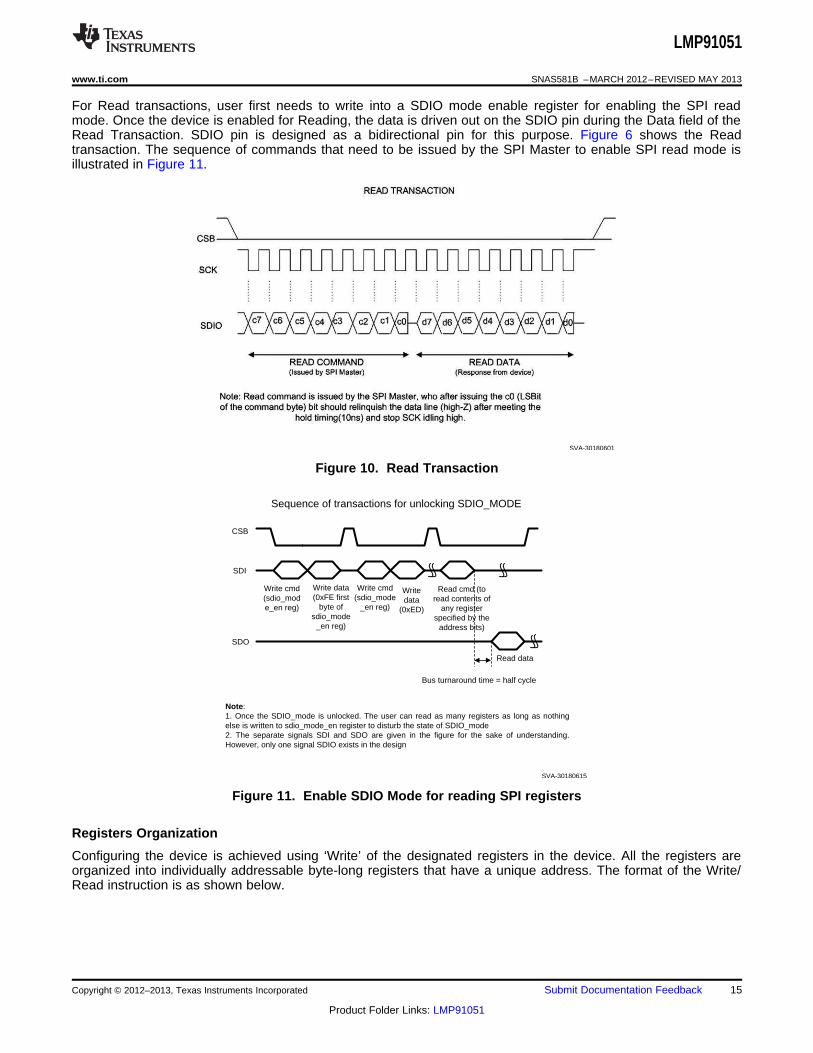
For Read transactions, user first needs to write into a SDIO mode enable register for enabling the SPI readmode. Once the device is enabled for Reading, the data is driven out on the SDIO pin during the Data field of theRead Transaction. SDIO pin is designed as a bidirectional pin for this purpose. Figure 6 shows the Readtransaction. The sequence of commands that need to be issued by the SPI Master to enable SPI read mode isillustrated in Figure 11.
Figure 10. Read Transaction
Figure 11. Enable SDIO Mode for reading SPI registers
Registers Organization
Configuring the device is achieved using ‘Write’ of the designated registers in the device. All the registers areorganized into individually addressable byte-long registers that have a unique address. The format of the Write/Read instruction is as shown below.
Copyright © 2012–2013, Texas Instruments Incorporated Submit Documentation Feedback 15
Product Folder Links: LMP91051
LMP91051
SNAS581B –MARCH 2012–REVISED MAY 2013 www.ti.com
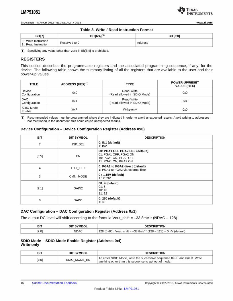
Table 3. Write / Read Instruction Format
BIT[7] BIT[6:4] (1) BIT[3:0]
0 : Write Instruction Reserved to 0 Address1 : Read Instruction
(1) Specifying any value other than zero in Bit[6:4] is prohibited.
REGISTERS
This section describes the programmable registers and the associated programming sequence, if any, for thedevice. The following table shows the summary listing of all the registers that are available to the user and theirpower-up values.
POWER-UP/RESETTITLE ADDRESS (HEX) (1) TYPE VALUE (HEX)
Device Read-Write0x0 0x0Configuration (Read allowed in SDIO Mode)
DAC Read-Write0x1 0x80Configuration (Read allowed in SDIO Mode)
SDIO Mode 0xF Write-only 0x0Enable
(1) Recommended values must be programmed where they are indicated in order to avoid unexpected results. Avoid writing to addressesnot mentioned in the document; this could cause unexpected results.
Device Configuration – Device Configuration Register (Address 0x0)
BIT BIT SYMBOL DESCRIPTION
0: IN1 (default)7 INP_SEL 1: IN2
00: PGA1 OFF PGA2 OFF (default)01: PGA1 OFF, PGA2 ON[6:5] EN 10: PGA1 ON, PGA2 OFF11: PGA1 ON, PGA2 ON
0: PGA1 to PGA2 direct (default)4 EXT_FILT 1: PGA1 to PGA2 via external filter
0 : 1.15V (default)3 CMN_MODE 1 : 2.59V
00: 4 (default)01: 8[2:1] GAIN2 10: 1611: 32
0: 250 (default)0 GAIN1 1: 42
DAC Configuration – DAC Configuration Register (Address 0x1)
The output DC level will shift according to the formula Vout_shift = –33.8mV * (NDAC – 128).
BIT BIT SYMBOL DESCRIPTION
[7:0] NDAC 128 (0×80): Vout_shift = –33.8mV * (128 – 128) = 0mV (default)
SDIO Mode – SDIO Mode Enable Register (Address 0xf)Write-only
BIT BIT SYMBOL DESCRIPTION
To enter SDIO Mode, write the successive sequence 0×FE and 0×ED. Write[7:0] SDIO_MODE_EN anything other than this sequence to get out of mode.
16 Submit Documentation Feedback Copyright © 2012–2013, Texas Instruments Incorporated
Product Folder Links: LMP91051

LMP91051
www.ti.com SNAS581B –MARCH 2012–REVISED MAY 2013
APPLICATION INFORMATION
NDIR Gas Sensing Principle
NDIR technology, a type of IR spectroscopy, is based on the principle that gas molecules absorb IR light andabsorption of a certain gas occurs at a specific wavelength. Typically, a thermopile with a built-in filter is used todetect the amount of a specific gas. For instance, since CO2 has a strong absorbance at a wavelength of 4.26µm, a band-pass filter is used to remove all light outside of this wavelength. Figure below shows the basic NDIRgas sensor working principle.
Figure 12. NDIR Gas Sensor Principle
Gas molecules will absorb radiation energy from the lamp emission. Absorption follows the Lambert-Beer law:
I = I0 * e-kcl
Where I is the transmitted IR intensity at the thermopile detector side, I0 is the initial intensity at the IR source, kis the gas specific absorption coefficient of the target gas, c is the gas concentration, and l is the length of theabsorption path from light source to thermopile detector.
The thermopile is used to detect the light intensity change. Its output voltage will follow:
V = n * Δα * (Tbody - Tamb)
Where Δα is the difference of the Seebeck coefficients of the thermopile materials and n is the number ofthermocouples in thermopile detector. Tbody is the blackbody temperature that is emitting thermal radiation (i.e.the IR lamp), and Tamb is the temperature of the surrounding ambient.
Inside the gas chamber, the IR lamp radiation energy could be regarded as ideal black body radiation. Theradiation emitted by a blackbody as a result of the temperature difference between the blackbody and ambient isknown as thermal radiation. According to Stefan-Boltzmann law, thermal radiation per unit area is expressed withthe following equation:
RT = σ * (Tbody4 - Tamb
4)
where σ = 5.67 * 10-8 W/(m2 *K4) is the Stefan-Boltzmann constant.
Assuming no loss in light intensity while traveling through the chamber, then RT = I. After rearranging theequations above the equation for thermopile output voltage becomes:
V = n * Δα * [ I0 * e-kcl ] / [σ * (Tbody2 + Tamb
2) * (Tbody + Tamb) ]
If we examine this equation it makes sense that the thermopile output voltage will be affected by the ambienttemperature and the IR lamp intensity uncertainty with a complex relationship. In order to maintain betteraccuracy of the system, special consideration should be taken in the design implementation. We can see thattemperature compensation is an effective way to maintain system accuracy. To accomplish this thermistors arecommonly integrated into the thermopile sensor and their resistance changes depending on the surroundingambient temperature. For better measurement accuracy, having a stable constant voltage to excite the thermistoris a good choice.
Traditional Discrete Op Amp Signal Conditioning
Traditionally discrete op amps have been employed for the gain stage of NDIR systems. AC coupling is requiredin order to eliminate the signal chain offset. To handle a two channel system one could use a quad op ampconfigured in a dual channel 2 stage front end. Active filtering is built into the signal path.
Copyright © 2012–2013, Texas Instruments Incorporated Submit Documentation Feedback 17
Product Folder Links: LMP91051

VDD
V+V-
U1A
R9
R7
C5
VREF
R8VREF
C6
C7
R10
VREFGND
V+V-
U1B
R12
R11VREF
C8
Reference Signal
ReferenceThermopile
V+V-
U1D
R3
R1
C1
VREF
R2VREF
C2
C3
R4
VREF
V+V-
U1C
R6
R5VREF
C4
Active Signal
Thermopile Active
LMP91051
SNAS581B –MARCH 2012–REVISED MAY 2013 www.ti.com
Figure 13. Discrete Op Amp Based System
LMP91051 Sensor AFE for NDIR Gas Sensing
An integrated analog front-end (AFE) can save design time and complexity by incorporating the features of adiscrete op amp solution into one chip. The LMP91051 AFE contains a two channel PGA which allows easyinterface to a two channel NDIR sensor. By cancelling out errors due to light source deviation optimum accuracyis obtained in a two channel system. This deviation results in long-term drift, which occurs over large periods oftime. Hence, the requirement to simultaneously sample both the reference and active channel simultaneously isnot required. You can use the input multiplexer (MUX) to switch between the two channels, reducing system costand complexity, while maintaining accuracy.
The LMP91051 also has fully programmable gain and offset adjustment. This helps ensure that the smallthermopile output (100’s µV) is matched to the dynamic range of the sampling Analog to Digital converter (A/D)and improves system resolution. The LMP91051 also provides a common mode bias which level-shifts thethermopile sensor signal away from the negative rail, allowing for accurate sensing in the presence of sensoroffset voltages.
18 Submit Documentation Feedback Copyright © 2012–2013, Texas Instruments Incorporated
Product Folder Links: LMP91051

VDD
GND
C4
A04
CMOUT3
OUT9
IN11
A15 CSB 10
GND6
VDD14
SDIO12
SCLK11
IN22
NC7
NC8
VIO 13
U1
LMP91051
C5
R3
C3
GND
COMMONR1
C1
GND
ADC1
GPIO1
AVCC
ADC2
ADC3
DVCC
MOSI
GPIO2 GND
CLK
U2
MSP430
NC
GND
Reference
Detector
Lamp + Thermi stor
Lamp -
U4
IRC-AT NDIR Sensor
VDD
Q1
GND
LAMP DRIVE
C2
GND
R2 TEMPERATURE
VDD
GND
V+
V-
U3R4
VDD
LAMP DRIVE
COMMON
TEM PER ATURE
GND
OUT
IN2
DAC
VREFCM GEN
G1=250,42 G2=4,8,16,32
SPI
VDD
LMP91051
CMOUT
+
- PGA1
+
- PGA2
A0 A1
IN1
SPI
GND
CSB
SCLK
SDIO
VIO
LMP91051
www.ti.com SNAS581B –MARCH 2012–REVISED MAY 2013
Figure 14. LMP91051 Sensor AFE for NDIR Sensing
LMP91051 Gas Detection System
Figure 15. LMP91051 CO2 Gas Detection System
The NDIR sensor used in the proposed system is a Alphasense IRC-AT. The sensor is composed of an IR lamp,two thermopile channels, and a thermistor which is used for temperature calibration. To save power and to avoidoverheating the device the lamp source is modulated typically with a 50% duty cycle with a frequency of 1 to3Hz. The Detector (Active) and Reference channel output are connected directly to the inputs of the LMP91051.Filter capacitors are connected from each input to the common mode reference, CMOUT, to provide low pass
Copyright © 2012–2013, Texas Instruments Incorporated Submit Documentation Feedback 19
Product Folder Links: LMP91051

+
- PGA2Gain
Active
Reference
Lamp Frequency 2Hz
Active
Reference
100Hz
LMP91051
SNAS581B –MARCH 2012–REVISED MAY 2013 www.ti.com
filtering. LMP91051 external filtering option is disabled and pins A0 and A1 are shorted internally in the chip. Nohigh pass filtering (AC coupling) is required because the internal offset DAC is used to cancel offset error in thesignal chain. This facilitates faster measurements over the traditional AC coupled system which will be discussedfurther later in this application note. The NDIR sensor has an internal thermistor which is connected to a resistorbridge then buffered by an amplifier.
The MSP430 microcontroller programs the LMP91051 via SPI. The microcontroller utilizes an internal 12 bitmuxed A/D to sample the LMP91051 output, buffered thermistor output, and system common mode. The entiresystem can be powered off of a single supply of 3V.
Gas Detection Method and Settings
In a 2 channel NDIR system the integrated IR lamp is pulsed (typical 1 to 3Hz) with a 50% duty cycle resulting insmall 100’s uV RC waveforms seen on both the output of the active and reference channel. To improvemeasurement accuracy these signals are amplified and the peak to peak waveform voltage of both the activechannel and reference channel are compared. In a DC coupled single supply system, active DC offsetadjustment is required in order to ensure the output of the gain stage doesn’t saturate and to remove signal chainoffset errors.
In a Muxed 2 channel system toggling between channels is done at an increased rate (i.e 100Hz) in order toreliably reconstruct both channels. To ensure accurate sampling, multiple samples should be taken on eachchannel prior to switching channels. Preferably sampling is synced to the lamp pulses to ensure data is beingcapture at the expected time relative to the lamp switching and the same sample within one lamp cycle can belooked at over many lamp cycles to determine noise performance. Figure below provides a visual explanation ofthe proposed gas detection method.
Figure 16. Example Gas Detection Method
A system was constructed with the following settings. Image below shows actual system RC waveform.
Lamp Pulse Frequency: 2 Hz
System Gain: 2000 V/V
System Offset: Apx. -700mV
Input Channel Mux Toggle Frequency: 100Hz
Number of Ch. Samples per Ch. Toggle: 10
ADC Sampling Rate: 1ksps
20 Submit Documentation Feedback Copyright © 2012–2013, Texas Instruments Incorporated
Product Folder Links: LMP91051

LMP91051
www.ti.com SNAS581B –MARCH 2012–REVISED MAY 2013
Figure 17. System Waveform
Copyright © 2012–2013, Texas Instruments Incorporated Submit Documentation Feedback 21
Product Folder Links: LMP91051

PACKAGE OPTION ADDENDUM
www.ti.com 7-May-2013
Addendum-Page 1
PACKAGING INFORMATION
Orderable Device Status(1)
Package Type PackageDrawing
Pins PackageQty
Eco Plan(2)
Lead/Ball Finish MSL Peak Temp(3)
Op Temp (°C) Top-Side Markings(4)
Samples
LMP91051MT/NOPB ACTIVE TSSOP PW 14 94 Green (RoHS& no Sb/Br)
CU SN Level-1-260C-UNLIM -40 to 105 LMP91051MT
LMP91051MTX/NOPB ACTIVE TSSOP PW 14 2500 Green (RoHS& no Sb/Br)
CU SN Level-1-260C-UNLIM -40 to 105 LMP91051MT
(1) The marketing status values are defined as follows:ACTIVE: Product device recommended for new designs.LIFEBUY: TI has announced that the device will be discontinued, and a lifetime-buy period is in effect.NRND: Not recommended for new designs. Device is in production to support existing customers, but TI does not recommend using this part in a new design.PREVIEW: Device has been announced but is not in production. Samples may or may not be available.OBSOLETE: TI has discontinued the production of the device.
(2) Eco Plan - The planned eco-friendly classification: Pb-Free (RoHS), Pb-Free (RoHS Exempt), or Green (RoHS & no Sb/Br) - please check http://www.ti.com/productcontent for the latest availabilityinformation and additional product content details.TBD: The Pb-Free/Green conversion plan has not been defined.Pb-Free (RoHS): TI's terms "Lead-Free" or "Pb-Free" mean semiconductor products that are compatible with the current RoHS requirements for all 6 substances, including the requirement thatlead not exceed 0.1% by weight in homogeneous materials. Where designed to be soldered at high temperatures, TI Pb-Free products are suitable for use in specified lead-free processes.Pb-Free (RoHS Exempt): This component has a RoHS exemption for either 1) lead-based flip-chip solder bumps used between the die and package, or 2) lead-based die adhesive used betweenthe die and leadframe. The component is otherwise considered Pb-Free (RoHS compatible) as defined above.Green (RoHS & no Sb/Br): TI defines "Green" to mean Pb-Free (RoHS compatible), and free of Bromine (Br) and Antimony (Sb) based flame retardants (Br or Sb do not exceed 0.1% by weightin homogeneous material)
(3) MSL, Peak Temp. -- The Moisture Sensitivity Level rating according to the JEDEC industry standard classifications, and peak solder temperature.
(4) Multiple Top-Side Markings will be inside parentheses. Only one Top-Side Marking contained in parentheses and separated by a "~" will appear on a device. If a line is indented then it is acontinuation of the previous line and the two combined represent the entire Top-Side Marking for that device.
Important Information and Disclaimer:The information provided on this page represents TI's knowledge and belief as of the date that it is provided. TI bases its knowledge and belief on informationprovided by third parties, and makes no representation or warranty as to the accuracy of such information. Efforts are underway to better integrate information from third parties. TI has taken andcontinues to take reasonable steps to provide representative and accurate information but may not have conducted destructive testing or chemical analysis on incoming materials and chemicals.TI and TI suppliers consider certain information to be proprietary, and thus CAS numbers and other limited information may not be available for release.
In no event shall TI's liability arising out of such information exceed the total purchase price of the TI part(s) at issue in this document sold by TI to Customer on an annual basis.

TAPE AND REEL INFORMATION
*All dimensions are nominal
Device PackageType
PackageDrawing
Pins SPQ ReelDiameter
(mm)
ReelWidth
W1 (mm)
A0(mm)
B0(mm)
K0(mm)
P1(mm)
W(mm)
Pin1Quadrant
LMP91051MTX/NOPB TSSOP PW 14 2500 330.0 12.4 6.95 5.6 1.6 8.0 12.0 Q1
PACKAGE MATERIALS INFORMATION
www.ti.com 6-Nov-2015
Pack Materials-Page 1

*All dimensions are nominal
Device Package Type Package Drawing Pins SPQ Length (mm) Width (mm) Height (mm)
LMP91051MTX/NOPB TSSOP PW 14 2500 367.0 367.0 35.0
PACKAGE MATERIALS INFORMATION
www.ti.com 6-Nov-2015
Pack Materials-Page 2


IMPORTANT NOTICE
Texas Instruments Incorporated and its subsidiaries (TI) reserve the right to make corrections, enhancements, improvements and otherchanges to its semiconductor products and services per JESD46, latest issue, and to discontinue any product or service per JESD48, latestissue. Buyers should obtain the latest relevant information before placing orders and should verify that such information is current andcomplete. All semiconductor products (also referred to herein as “components”) are sold subject to TI’s terms and conditions of salesupplied at the time of order acknowledgment.TI warrants performance of its components to the specifications applicable at the time of sale, in accordance with the warranty in TI’s termsand conditions of sale of semiconductor products. Testing and other quality control techniques are used to the extent TI deems necessaryto support this warranty. Except where mandated by applicable law, testing of all parameters of each component is not necessarilyperformed.TI assumes no liability for applications assistance or the design of Buyers’ products. Buyers are responsible for their products andapplications using TI components. To minimize the risks associated with Buyers’ products and applications, Buyers should provideadequate design and operating safeguards.TI does not warrant or represent that any license, either express or implied, is granted under any patent right, copyright, mask work right, orother intellectual property right relating to any combination, machine, or process in which TI components or services are used. Informationpublished by TI regarding third-party products or services does not constitute a license to use such products or services or a warranty orendorsement thereof. Use of such information may require a license from a third party under the patents or other intellectual property of thethird party, or a license from TI under the patents or other intellectual property of TI.Reproduction of significant portions of TI information in TI data books or data sheets is permissible only if reproduction is without alterationand is accompanied by all associated warranties, conditions, limitations, and notices. TI is not responsible or liable for such altereddocumentation. Information of third parties may be subject to additional restrictions.Resale of TI components or services with statements different from or beyond the parameters stated by TI for that component or servicevoids all express and any implied warranties for the associated TI component or service and is an unfair and deceptive business practice.TI is not responsible or liable for any such statements.Buyer acknowledges and agrees that it is solely responsible for compliance with all legal, regulatory and safety-related requirementsconcerning its products, and any use of TI components in its applications, notwithstanding any applications-related information or supportthat may be provided by TI. Buyer represents and agrees that it has all the necessary expertise to create and implement safeguards whichanticipate dangerous consequences of failures, monitor failures and their consequences, lessen the likelihood of failures that might causeharm and take appropriate remedial actions. Buyer will fully indemnify TI and its representatives against any damages arising out of the useof any TI components in safety-critical applications.In some cases, TI components may be promoted specifically to facilitate safety-related applications. With such components, TI’s goal is tohelp enable customers to design and create their own end-product solutions that meet applicable functional safety standards andrequirements. Nonetheless, such components are subject to these terms.No TI components are authorized for use in FDA Class III (or similar life-critical medical equipment) unless authorized officers of the partieshave executed a special agreement specifically governing such use.Only those TI components which TI has specifically designated as military grade or “enhanced plastic” are designed and intended for use inmilitary/aerospace applications or environments. Buyer acknowledges and agrees that any military or aerospace use of TI componentswhich have not been so designated is solely at the Buyer's risk, and that Buyer is solely responsible for compliance with all legal andregulatory requirements in connection with such use.TI has specifically designated certain components as meeting ISO/TS16949 requirements, mainly for automotive use. In any case of use ofnon-designated products, TI will not be responsible for any failure to meet ISO/TS16949.
Products ApplicationsAudio www.ti.com/audio Automotive and Transportation www.ti.com/automotiveAmplifiers amplifier.ti.com Communications and Telecom www.ti.com/communicationsData Converters dataconverter.ti.com Computers and Peripherals www.ti.com/computersDLP® Products www.dlp.com Consumer Electronics www.ti.com/consumer-appsDSP dsp.ti.com Energy and Lighting www.ti.com/energyClocks and Timers www.ti.com/clocks Industrial www.ti.com/industrialInterface interface.ti.com Medical www.ti.com/medicalLogic logic.ti.com Security www.ti.com/securityPower Mgmt power.ti.com Space, Avionics and Defense www.ti.com/space-avionics-defenseMicrocontrollers microcontroller.ti.com Video and Imaging www.ti.com/videoRFID www.ti-rfid.comOMAP Applications Processors www.ti.com/omap TI E2E Community e2e.ti.comWireless Connectivity www.ti.com/wirelessconnectivity
Mailing Address: Texas Instruments, Post Office Box 655303, Dallas, Texas 75265Copyright © 2015, Texas Instruments Incorporated