LMH6601 and LMH6601-Q1 250-MHz, 2.4-V CMOS · PDF fileOUTPUT V-+IN V +-IN +-1 2 3 5 4 6 SD...
40
1 10 100 1000 FREQUENCY (MHz -1 0 1 2 3 4 5 6 7 MAGNITUDE (dB) 2.7V 3.3V 5V Product Folder Sample & Buy Technical Documents Tools & Software Support & Community LMH6601, LMH6601-Q1 SNOSAK9F – JUNE 2006 – REVISED JUNE 2015 LMH6601 and LMH6601-Q1 250-MHz, 2.4-V CMOS Operational Amplifier With Shutdown 1 Features 3 Description The LMH6601 device is a low-voltage (2.4 V to 5.5 1• LMH6601-Q1 Qualified for Automotive V), high-speed voltage feedback operational amplifier Applications suitable for use in a variety of consumer and – AEC-Q100 Grade 3 industrial applications. With a bandwidth of 125 MHz – –40°C to 85°C Ambient Operating at a gain of +2 and ensured high-output current of 100 mA, the LMH6601 is an ideal choice for video Temperature Range line driver applications, including HDTV. Low-input • V S = 3.3 V, T A = 25°C, A V = 2 V/V, R L = 150 Ω to bias current (50 pA maximum), rail-to-rail output, and V − , Unless Specified low current noise allow the use of the LMH6601 in • 125 MHz −3 dB Small Signal Bandwidth various industrial applications such as transimpedance amplifiers, active filters, or high- • 75 MHz −3 dB Large Signal Bandwidth impedance buffers. The LMH6601 is an attractive • 30 MHz Large Signal 0.1-dB Gain Flatness solution for systems which require high performance • 260 V/μs Slew Rate at low supply voltages. The LMH6601 is available in a • 0.25%/0.25° Differential Gain and Differential 6-pin SC70 package, and includes a micropower Phase shutdown feature. • Rail-to-Rail Output Device Information (1) • 2.4-V to 5.5-V Single-Supply Operating Range PART NUMBER PACKAGE BODY SIZE (NOM) • 6-Pin SC70 Package LMH6601 SC70 (6) 2.00 mm × 1.25 mm LMH6601-Q1 2 Applications (1) For all available packages, see the orderable addendum at • Video Amplifiers the end of the data sheet. • Charge Amplifiers Response at a Gain of +2 • Set-Top Boxes for Various Supply Voltages • Sample and Holds • Transimpedance Amplifiers • Line Drivers • High-Impedance Buffers • Automotive 1 An IMPORTANT NOTICE at the end of this data sheet addresses availability, warranty, changes, use in safety-critical applications, intellectual property matters and other important disclaimers. PRODUCTION DATA.
Transcript of LMH6601 and LMH6601-Q1 250-MHz, 2.4-V CMOS · PDF fileOUTPUT V-+IN V +-IN +-1 2 3 5 4 6 SD...

1 10 100 1000
FREQUENCY (MHz
-1
0
1
2
3
4
5
6
7
MA
GN
ITU
DE
(dB
) 2.7V
3.3V
5V
Product
Folder
Sample &Buy
Technical
Documents
Tools &
Software
Support &Community
LMH6601, LMH6601-Q1SNOSAK9F –JUNE 2006–REVISED JUNE 2015
LMH6601 and LMH6601-Q1 250-MHz, 2.4-V CMOS Operational Amplifier With Shutdown1 Features 3 Description
The LMH6601 device is a low-voltage (2.4 V to 5.51• LMH6601-Q1 Qualified for Automotive
V), high-speed voltage feedback operational amplifierApplicationssuitable for use in a variety of consumer and
– AEC-Q100 Grade 3 industrial applications. With a bandwidth of 125 MHz– –40°C to 85°C Ambient Operating at a gain of +2 and ensured high-output current of
100 mA, the LMH6601 is an ideal choice for videoTemperature Rangeline driver applications, including HDTV. Low-input• VS = 3.3 V, TA = 25°C, AV = 2 V/V, RL = 150 Ω tobias current (50 pA maximum), rail-to-rail output, andV−, Unless Specified low current noise allow the use of the LMH6601 in
• 125 MHz −3 dB Small Signal Bandwidth various industrial applications such astransimpedance amplifiers, active filters, or high-• 75 MHz −3 dB Large Signal Bandwidthimpedance buffers. The LMH6601 is an attractive• 30 MHz Large Signal 0.1-dB Gain Flatnesssolution for systems which require high performance
• 260 V/μs Slew Rate at low supply voltages. The LMH6601 is available in a• 0.25%/0.25° Differential Gain and Differential 6-pin SC70 package, and includes a micropower
Phase shutdown feature.• Rail-to-Rail Output
Device Information(1)• 2.4-V to 5.5-V Single-Supply Operating Range
PART NUMBER PACKAGE BODY SIZE (NOM)• 6-Pin SC70 Package
LMH6601SC70 (6) 2.00 mm × 1.25 mm
LMH6601-Q12 Applications(1) For all available packages, see the orderable addendum at• Video Amplifiers the end of the data sheet.
• Charge AmplifiersResponse at a Gain of +2• Set-Top Boxes
for Various Supply Voltages• Sample and Holds• Transimpedance Amplifiers• Line Drivers• High-Impedance Buffers• Automotive
1
An IMPORTANT NOTICE at the end of this data sheet addresses availability, warranty, changes, use in safety-critical applications,intellectual property matters and other important disclaimers. PRODUCTION DATA.

LMH6601, LMH6601-Q1SNOSAK9F –JUNE 2006–REVISED JUNE 2015 www.ti.com
Table of Contents7.1 Overview ................................................................. 201 Features .................................................................. 17.2 Feature Description................................................. 202 Applications ........................................................... 17.3 Device Functional Modes........................................ 213 Description ............................................................. 1
8 Application and Implementation ........................ 234 Revision History..................................................... 28.1 Application Information............................................ 235 Pin Configuration and Functions ......................... 38.2 Typical Application .................................................. 296 Specifications......................................................... 3
9 Power Supply Recommendations ...................... 326.1 Absolute Maximum Ratings ...................................... 310 Layout................................................................... 326.2 ESD Ratings - for LMH6601 ..................................... 3
10.1 Layout Guidelines ................................................. 326.3 ESD Ratings - for LMH6601-Q1 ............................... 410.2 Layout Examples................................................... 326.4 Recommended Operating Conditions....................... 4
11 Device and Documentation Support ................. 336.5 Thermal Information .................................................. 411.1 Documentation Support ........................................ 336.6 Electrical Characteristics, 5 V ................................... 411.2 Related Links ........................................................ 336.7 Electrical Characteristics, 3.3 V ................................ 611.3 Community Resources.......................................... 336.8 Electrical Characteristics, 2.7 V ................................ 811.4 Trademarks ........................................................... 336.9 Switching Characteristics, 5 V ................................ 1011.5 Electrostatic Discharge Caution............................ 336.10 Switching Characteristics, 3.3 V ........................... 1111.6 Glossary ................................................................ 336.11 Switching Characteristics, 2.7 V ........................... 11
12 Mechanical, Packaging, and Orderable6.12 Typical Characteristics .......................................... 12Information ........................................................... 337 Detailed Description ............................................ 20
4 Revision HistoryNOTE: Page numbers for previous revisions may differ from page numbers in the current version.
Changes from Revision E (March 2013) to Revision F Page
• Added Pin Configuration and Functions section, ESD Ratings table, Feature Description section, Device FunctionalModes, Application and Implementation section, Power Supply Recommendations section, Layout section, Deviceand Documentation Support section, and Mechanical, Packaging, and Orderable Information section .............................. 1
• Removed IOS over temperature limit in Electrical Characteristics, 2.7 V ............................................................................... 8• Moved the SAG Compensation section to the Typical Application section.......................................................................... 25• Changed section titled Other Applications to Charge Preamplifier ..................................................................................... 28
Changes from Revision D (March 2013) to Revision E Page
• Changed layout of National Data Sheet to TI format ............................................................................................................. 1
2 Submit Documentation Feedback Copyright © 2006–2015, Texas Instruments Incorporated
Product Folder Links: LMH6601 LMH6601-Q1

OUTPUT
V-
+IN
V+
-IN
+ -
1
2
3
5
4
6
SD
LMH6601, LMH6601-Q1www.ti.com SNOSAK9F –JUNE 2006–REVISED JUNE 2015
5 Pin Configuration and Functions
DCK Package6-Pin SC70Top View
Pin FunctionsPIN
I/O DESCRIPTIONNO. NAME1 OUTPUT O Output2 V- I Negative supply3 +IN I Noninverting input4 -IN I Inverting input5 SD I Shutdown6 V+ I Positive supply
6 Specifications
6.1 Absolute Maximum Ratings (1)
MIN MAX UNITVIN Differential ±2.5 VInput Current (2) ±10 mAOutput Current 200 mA (3) mASupply Voltage (V+ – V−) 6 VVoltage at Input/Output Pins V++0.5, VV−−0.5Junction Temperature 150 °C
Infrared or Convection (20 sec.) 235Soldering Information °C
Wave Soldering (10 sec.) 260Storage Temperature −65 150 °C
(1) Stresses beyond those listed under Absolute Maximum Ratings may cause permanent damage to the device. These are stress ratingsonly, which do not imply functional operation of the device at these or any other conditions beyond those indicated under RecommendedOperating Conditions. Exposure to absolute-maximum-rated conditions for extended periods may affect device reliability.
(2) Negative input current implies current flowing out of the device.(3) The maximum continuous output current (IOUT) is determined by device power dissipation limitations.
6.2 ESD Ratings - for LMH6601VALUE UNIT
Human body model (HBM), per ANSI/ESDA/JEDEC JS-001 (1) ±2000V(ESD) Electrostatic discharge VCharged-device model (CDM), per JEDEC specification JESD22- ±1000C101 (2)
(1) Human Body Model, applicable std. MIL-STD-883, Method 3015.7.(2) JEDEC document JEP157 states that 250-V CDM allows safe manufacturing with a standard ESD control process.
Copyright © 2006–2015, Texas Instruments Incorporated Submit Documentation Feedback 3
Product Folder Links: LMH6601 LMH6601-Q1
LMH6601, LMH6601-Q1SNOSAK9F –JUNE 2006–REVISED JUNE 2015 www.ti.com
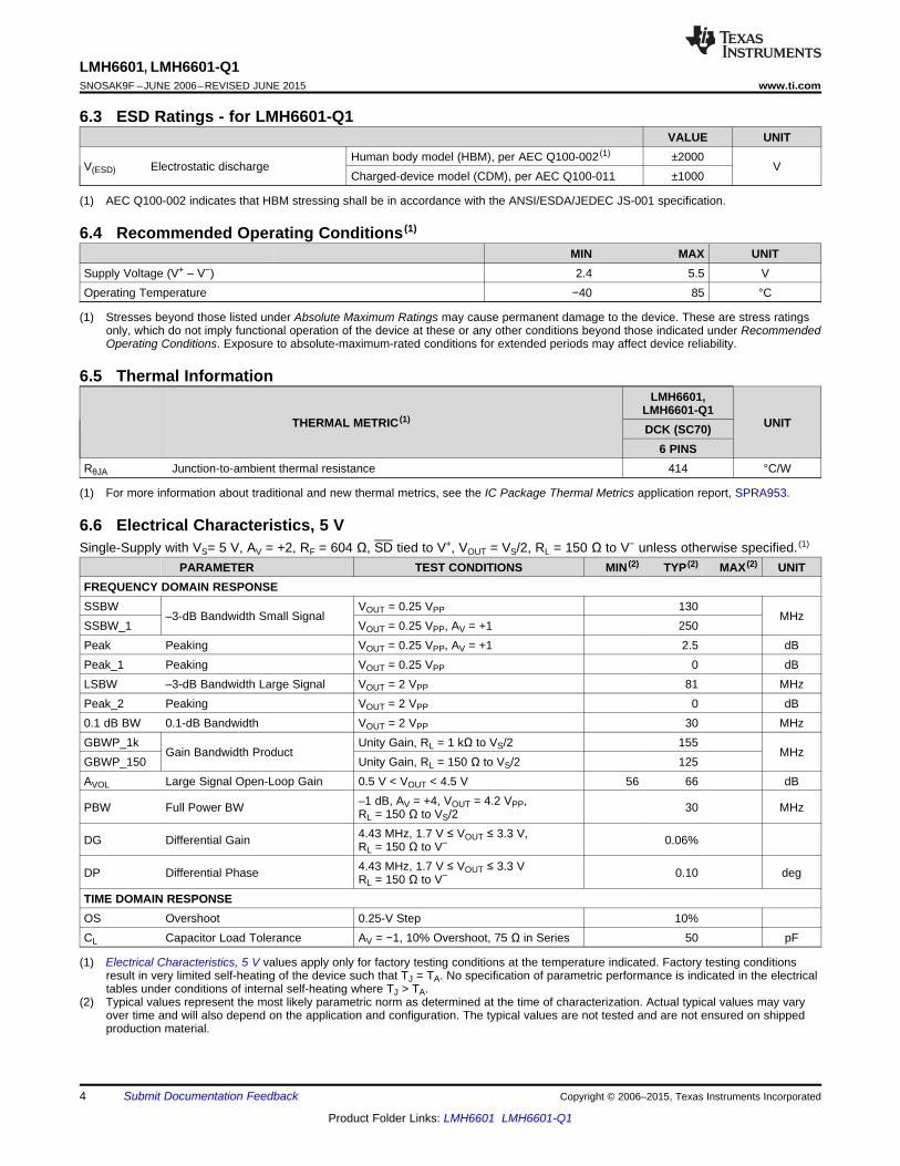
6.3 ESD Ratings - for LMH6601-Q1VALUE UNIT
Human body model (HBM), per AEC Q100-002 (1) ±2000V(ESD) Electrostatic discharge V
Charged-device model (CDM), per AEC Q100-011 ±1000
(1) AEC Q100-002 indicates that HBM stressing shall be in accordance with the ANSI/ESDA/JEDEC JS-001 specification.
6.4 Recommended Operating Conditions (1)
MIN MAX UNITSupply Voltage (V+ – V−) 2.4 5.5 VOperating Temperature −40 85 °C
(1) Stresses beyond those listed under Absolute Maximum Ratings may cause permanent damage to the device. These are stress ratingsonly, which do not imply functional operation of the device at these or any other conditions beyond those indicated under RecommendedOperating Conditions. Exposure to absolute-maximum-rated conditions for extended periods may affect device reliability.
6.5 Thermal InformationLMH6601,
LMH6601-Q1THERMAL METRIC (1) UNITDCK (SC70)
6 PINSRθJA Junction-to-ambient thermal resistance 414 °C/W
(1) For more information about traditional and new thermal metrics, see the IC Package Thermal Metrics application report, SPRA953.
6.6 Electrical Characteristics, 5 VSingle-Supply with VS= 5 V, AV = +2, RF = 604 Ω, SD tied to V+, VOUT = VS/2, RL = 150 Ω to V− unless otherwise specified. (1)
PARAMETER TEST CONDITIONS MIN (2) TYP (2) MAX (2) UNITFREQUENCY DOMAIN RESPONSESSBW VOUT = 0.25 VPP 130
–3-dB Bandwidth Small Signal MHzSSBW_1 VOUT = 0.25 VPP, AV = +1 250Peak Peaking VOUT = 0.25 VPP, AV = +1 2.5 dBPeak_1 Peaking VOUT = 0.25 VPP 0 dBLSBW –3-dB Bandwidth Large Signal VOUT = 2 VPP 81 MHzPeak_2 Peaking VOUT = 2 VPP 0 dB0.1 dB BW 0.1-dB Bandwidth VOUT = 2 VPP 30 MHzGBWP_1k Unity Gain, RL = 1 kΩ to VS/2 155
Gain Bandwidth Product MHzGBWP_150 Unity Gain, RL = 150 Ω to VS/2 125AVOL Large Signal Open-Loop Gain 0.5 V < VOUT < 4.5 V 56 66 dB
–1 dB, AV = +4, VOUT = 4.2 VPP,PBW Full Power BW 30 MHzRL = 150 Ω to VS/24.43 MHz, 1.7 V ≤ VOUT ≤ 3.3 V,DG Differential Gain 0.06%RL = 150 Ω to V−
4.43 MHz, 1.7 V ≤ VOUT ≤ 3.3 VDP Differential Phase 0.10 degRL = 150 Ω to V−
TIME DOMAIN RESPONSEOS Overshoot 0.25-V Step 10%CL Capacitor Load Tolerance AV = −1, 10% Overshoot, 75 Ω in Series 50 pF
(1) Electrical Characteristics, 5 V values apply only for factory testing conditions at the temperature indicated. Factory testing conditionsresult in very limited self-heating of the device such that TJ = TA. No specification of parametric performance is indicated in the electricaltables under conditions of internal self-heating where TJ > TA.
(2) Typical values represent the most likely parametric norm as determined at the time of characterization. Actual typical values may varyover time and will also depend on the application and configuration. The typical values are not tested and are not ensured on shippedproduction material.
4 Submit Documentation Feedback Copyright © 2006–2015, Texas Instruments Incorporated
Product Folder Links: LMH6601 LMH6601-Q1

LMH6601, LMH6601-Q1www.ti.com SNOSAK9F –JUNE 2006–REVISED JUNE 2015
Electrical Characteristics, 5 V (continued)Single-Supply with VS= 5 V, AV = +2, RF = 604 Ω, SD tied to V+, VOUT = VS/2, RL = 150 Ω to V− unless otherwise specified.(1)
PARAMETER TEST CONDITIONS MIN (2) TYP (2) MAX (2) UNITDISTORTION and NOISE PERFORMANCEHD2 2 VPP, 10 MHz −56
Harmonic Distortion (2nd) dBcHD2_1 4 VPP, 10 MHz, RL = 1 kΩ to VS/2 −61HD3 2 VPP, 10 MHz −73
Harmonic Distortion (3rd) dBcHD3_1 4 VPP, 10 MHz, RL = 1 kΩ to VS/2 −64THD Total Harmonic Distortion 4 VPP, 10 MHz, RL = 1 kΩ to VS/2 −58VN1 >10 MHz 7
Input Voltage Noise nV/√HzVN2 1 MHz 10IN Input Current Noise >1 MHz 50 fA/√HzSTATIC, DC PERFORMANCE
±1 ±2.4VIO Input Offset Voltage mV
At temperature extremes ±5DVIO Input Offset Voltage Average Drift See (3) −5 μV/°CIB Input Bias Current See (4) 5 50 pAIOS Input Offset Current See (4) 2 25 pARIN Input Resistance 0 V ≤ VIN ≤ 3.5 V 10 TΩCIN Input Capacitance 1.3 pF
55 59Positive Power Supply Rejection+PSRR DC dBAt temperatureRatio 51extremes
53 61Negative Power Supply Rejection−PSRR DC dBAt temperatureRatio 50extremes
56 68CMRR Common-Mode Rejection Ratio DC dBAt temperature 53extremes
CMRR > 50 dB (At temperatureCMVR Input Voltage Range V− – 0.20 – V+ – 1.5 Vextremes)9.6 11.5
Normal Operation mAAt temperatureVOUT = VS/2 13.5ICC Supply Current extremesShutdown 100 nASD tied to ≤ 0.5 V (5)
–210 –190VOH1 RL = 150 Ω to V– At temperature –480extremes
Output High VoltageVOH2 RL = 75 Ω to VS/2 –190 mV(Relative to V+)–60 –12
VOH3 RL = 10 kΩ to V– At temperature –110extremes
(3) Drift determined by dividing the change in parameter at temperature extremes by the total temperature change.(4) This parameter is ensured by design and/or characterization and is not tested in production.(5) SD logic is CMOS compatible. To ensure proper logic level and to minimize power supply current, SD should typically be less than 10%
of total supply voltage away from either supply rail.
Copyright © 2006–2015, Texas Instruments Incorporated Submit Documentation Feedback 5
Product Folder Links: LMH6601 LMH6601-Q1

LMH6601, LMH6601-Q1SNOSAK9F –JUNE 2006–REVISED JUNE 2015 www.ti.com
Electrical Characteristics, 5 V (continued)Single-Supply with VS= 5 V, AV = +2, RF = 604 Ω, SD tied to V+, VOUT = VS/2, RL = 150 Ω to V− unless otherwise specified.(1)
PARAMETER TEST CONDITIONS MIN (2) TYP (2) MAX (2) UNIT5 45
VOL1 RL = 150 Ω to V– At temperature 125extremesOutput Low VoltageVOL2 RL = 75 Ω to VS/2 120 mV(Relative to V–)
5 45VOL3 RL = 10 kΩ to V– At temperature 125extremes
Source 150VOUT < 0.6 V fromIO Respective Supply Sink 180Output Current mAVOUT = VS/2,IO_1 ±100VID = ±18 mV (6)
THD < −30 dBc, f = 200 kHz,Load Output Load Rating 20 ΩRL tied to VS/2, VOUT = 4 VPP
RO_Enabled Output Resistance Enabled, AV = +1 0.2 ΩRO_Disabled Output Resistance Shutdown >100 MΩCO_Disabled Output Capacitance Shutdown 5 pFMISCELLANEOUS PERFORMANCEVDMAX Voltage Limit for Disable (Pin 5) See (5) (At temperature extremes) 0 0.5 VVDMIN Voltage Limit for Enable (Pin 5) See (5) (At temperature extremes) 4.5 5 VIi Logic Input Current (Pin 5) SD = 5 V (5) 10 pAV_glitch Turnon Glitch 2.2 VIsolationOFF Off Isolation 1 MHz, RL = 1 kΩ 60 dB
(6) “VID” is input differential voltage (input overdrive).
6.7 Electrical Characteristics, 3.3 VSingle-Supply with VS= 3.3 V, AV = +2, RF = 604Ω, SD tied to V+, VOUT = VS/2, RL = 150 Ω to V− unless otherwise specified. (1)
PARAMETER TEST CONDITIONS MIN (2) TYP (2) MAX (2) UNITFREQUENCY DOMAIN RESPONSESSBW VOUT = 0.25 VPP 125
–3-dB Bandwidth Small Signal MHzSSBW_1 VOUT = 0.25 VPP, AV = +1 250Peak Peaking VOUT = 0.25 VPP, AV = +1 3 dBPeak_1 Peaking VOUT = 0.25 VPP 0.05 dBLSBW –3-dB Bandwidth Large Signal VOUT = 2 V PP 75 MHzPeak_2 Peaking VOUT = 2 VPP 0 dB0.1 dB BW 0.1-dB Bandwidth VOUT = 2 VPP 30 MHzGBWP_1k Unity Gain, RL = 1 kΩ to VS/2 115
Gain Bandwidth Product MHzGBWP_150 Unity Gain, RL = 150 Ω to VS/2 105AVOL Large Signal Open-Loop Gain 0.3 V < VOUT < 3 V 56 67 dB
–1 dB, AV = +4, VOUT = 2.8 VPP,PBW Full Power BW 30 MHzRL = 150 Ω to VS/24.43 MHz, 0.85 V ≤ VOUT ≤ 2.45 V,DG Differential Gain 0.06%RL = 150 Ω to V−
4.43 MHz, 0.85 V ≤ VOUT ≤ 2.45 VDP Differential Phase 0.23 degRL = 150 Ω to V−
(1) Electrical Characteristics, 3.3 V values apply only for factory testing conditions at the temperature indicated. Factory testing conditionsresult in very limited self-heating of the device such that TJ = TA. No specification of parametric performance is indicated in the electricaltables under conditions of internal self-heating where TJ > TA.
(2) Typical values represent the most likely parametric norm as determined at the time of characterization. Actual typical values may varyover time and will also depend on the application and configuration. The typical values are not tested and are not ensured on shippedproduction material.
6 Submit Documentation Feedback Copyright © 2006–2015, Texas Instruments Incorporated
Product Folder Links: LMH6601 LMH6601-Q1
LMH6601, LMH6601-Q1www.ti.com SNOSAK9F –JUNE 2006–REVISED JUNE 2015
Electrical Characteristics, 3.3 V (continued)Single-Supply with VS= 3.3 V, AV = +2, RF = 604Ω, SD tied to V+, VOUT = VS/2, RL = 150 Ω to V− unless otherwise specified.(1)
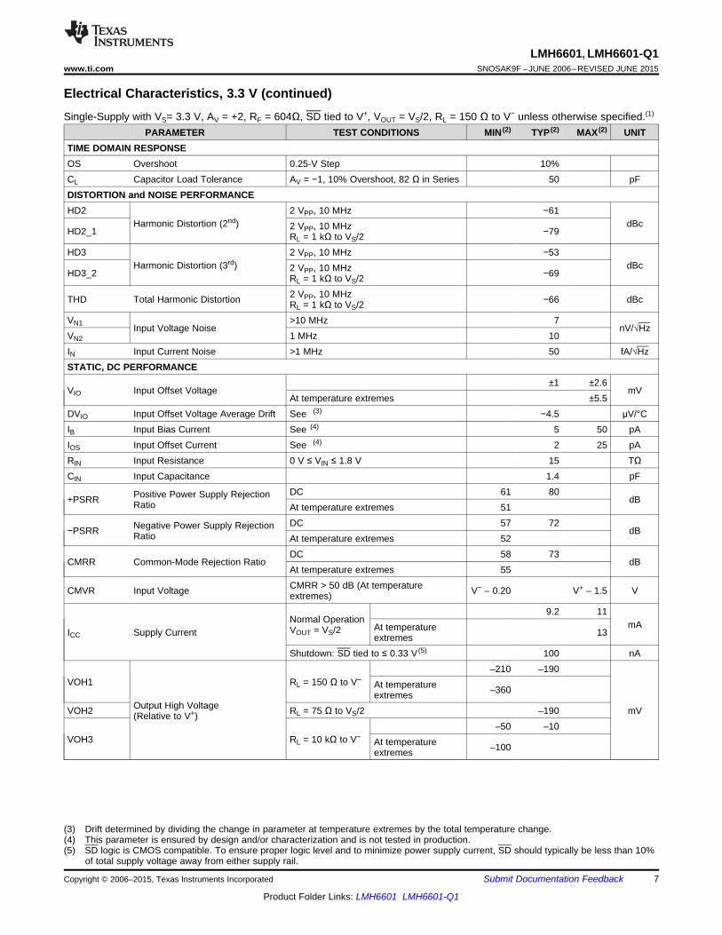
PARAMETER TEST CONDITIONS MIN (2) TYP (2) MAX (2) UNITTIME DOMAIN RESPONSEOS Overshoot 0.25-V Step 10%CL Capacitor Load Tolerance AV = −1, 10% Overshoot, 82 Ω in Series 50 pFDISTORTION and NOISE PERFORMANCEHD2 2 VPP, 10 MHz −61
Harmonic Distortion (2nd) dBc2 VPP, 10 MHzHD2_1 −79RL = 1 kΩ to VS/2HD3 2 VPP, 10 MHz −53
Harmonic Distortion (3rd) dBc2 VPP, 10 MHzHD3_2 −69RL = 1 kΩ to VS/22 VPP, 10 MHzTHD Total Harmonic Distortion −66 dBcRL = 1 kΩ to VS/2
VN1 >10 MHz 7Input Voltage Noise nV/√Hz
VN2 1 MHz 10IN Input Current Noise >1 MHz 50 fA/√HzSTATIC, DC PERFORMANCE
±1 ±2.6VIO Input Offset Voltage mV
At temperature extremes ±5.5DVIO Input Offset Voltage Average Drift See (3) −4.5 μV/°CIB Input Bias Current See (4) 5 50 pAIOS Input Offset Current See (4) 2 25 pARIN Input Resistance 0 V ≤ VIN ≤ 1.8 V 15 TΩCIN Input Capacitance 1.4 pF
DC 61 80Positive Power Supply Rejection+PSRR dBRatio At temperature extremes 51DC 57 72Negative Power Supply Rejection−PSRR dBRatio At temperature extremes 52DC 58 73
CMRR Common-Mode Rejection Ratio dBAt temperature extremes 55CMRR > 50 dB (At temperatureCMVR Input Voltage V− – 0.20 V+ – 1.5 Vextremes)
9.2 11Normal Operation mAAt temperatureVOUT = VS/2ICC Supply Current 13extremesShutdown: SD tied to ≤ 0.33 V (5) 100 nA
–210 –190VOH1 RL = 150 Ω to V– At temperature –360extremes
Output High VoltageVOH2 RL = 75 Ω to VS/2 –190 mV(Relative to V+)–50 –10
VOH3 RL = 10 kΩ to V− At temperature –100extremes
(3) Drift determined by dividing the change in parameter at temperature extremes by the total temperature change.(4) This parameter is ensured by design and/or characterization and is not tested in production.(5) SD logic is CMOS compatible. To ensure proper logic level and to minimize power supply current, SD should typically be less than 10%
of total supply voltage away from either supply rail.
Copyright © 2006–2015, Texas Instruments Incorporated Submit Documentation Feedback 7
Product Folder Links: LMH6601 LMH6601-Q1

LMH6601, LMH6601-Q1SNOSAK9F –JUNE 2006–REVISED JUNE 2015 www.ti.com
Electrical Characteristics, 3.3 V (continued)Single-Supply with VS= 3.3 V, AV = +2, RF = 604Ω, SD tied to V+, VOUT = VS/2, RL = 150 Ω to V− unless otherwise specified.(1)
PARAMETER TEST CONDITIONS MIN (2) TYP (2) MAX (2) UNIT4 45
VOL1 RL = 150 Ω to V– At temperature 125extremesOutput Low VoltageVOL2 RL = 75 Ω to VS/2 105 mV(Relative to V–)
4 45VOL3 RL = 10 kΩ to V– At temperature 125extremes
VOUT < 0.6 V from Source 50IO Respective
Output Current Sink 75 mASupplyIO_1 VOUT = VS/2, VID = ±18 mV (6) ±75
THD < −30 dBc, f = 200 kHz,Load Output Load Rating 25 ΩRL tied to VS/2, VOUT = 2.6 VPP
RO_Enabled Output Resistance Enabled, AV = +1 0.2 ΩRO_Disabled Output Resistance Shutdown >100 MΩCO_Disabled Output Capacitance Shutdown 5.6 pFMISCELLANEOUS PERFORMANCEVDMAX Voltage Limit for Disable (Pin 5) See (5) (At temperature extremes) 0 0.33 VVDMIN Voltage Limit for Enable (Pin 5) See (5) (At temperature extremes) 2.97 3.3 VIi Logic Input Current (Pin 5) SD = 3.3 V (5) 8 pAV_glitch Turnon Glitch 1.6 VIsolationOFF Off Isolation 1 MHz, RL = 1 kΩ 60 dB
(6) “VID” is input differential voltage (input overdrive).
6.8 Electrical Characteristics, 2.7 VSingle-Supply with VS = 2.7 V, AV = +2, RF = 604 Ω, SD tied to V+, VOUT = VS/2, RL = 150 Ω to V− unless otherwisespecified. (1)
PARAMETER TEST CONDITIONS MIN (2) TYP (2) MAX (2) UNITFREQUENCY DOMAIN RESPONSESSBW VOUT = 0.25 VPP 120
–3-dB Bandwidth Small Signal MHzSSBW_1 VOUT = 0.25 VPP, AV = +1 250Peak Peaking VOUT = 0.25 VPP, AV = +1 3.1 dBPeak_1 Peaking VOUT = 0.25 VPP 0.1 dBLSBW –3-dB Bandwidth Large Signal VOUT = 2 V PP 73 MHzPeak_2 Peaking VOUT = 2 VPP 0 dB0.1 dB BW 0.1-dB Bandwidth VOUT = 2 VPP 30 MHzGBWP_1k Unity Gain, RL = 1 kΩ to VS/2 110
Gain Bandwidth Product MHzGBWP_150 Unity Gain, RL = 150 Ω to VS/2 81AVOL Large Signal Open-Loop Gain 0.25 V < VOUT < 2.5 V 56 65 dB
–1 dB, AV = +4, VOUT = 2 VPP,PBW Full Power BW 13 MHzRL = 150 Ω to VS/24.43 MHz, 0.45 V ≤ VOUT ≤ 2.05 VDG Differential Gain 0.12%RL = 150 Ω to V−
(1) Electrical Characteristics, 2.7 V values apply only for factory testing conditions at the temperature indicated. Factory testing conditionsresult in very limited self-heating of the device such that TJ = TA. No specification of parametric performance is indicated in the electricaltables under conditions of internal self-heating where TJ > TA.
(2) Typical values represent the most likely parametric norm as determined at the time of characterization. Actual typical values may varyover time and will also depend on the application and configuration. The typical values are not tested and are not ensured on shippedproduction material.
8 Submit Documentation Feedback Copyright © 2006–2015, Texas Instruments Incorporated
Product Folder Links: LMH6601 LMH6601-Q1

LMH6601, LMH6601-Q1www.ti.com SNOSAK9F –JUNE 2006–REVISED JUNE 2015
Electrical Characteristics, 2.7 V (continued)Single-Supply with VS = 2.7 V, AV = +2, RF = 604 Ω, SD tied to V+, VOUT = VS/2, RL = 150 Ω to V− unless otherwisespecified.(1)
PARAMETER TEST CONDITIONS MIN (2) TYP (2) MAX (2) UNIT4.43 MHz, 0.45 V ≤ VOUT ≤ 2.05 VDP Differential Phase 0.62 degRL = 150 Ω to V−
TIME DOMAIN RESPONSEOS Overshoot 0.25-V Step 10%DISTORTION and NOISE PERFORMANCEHD2 Harmonic Distortion (2nd) 1 VPP, 10 MHz −58 dBcHD3 Harmonic Distortion (3rd) 1 VPP, 10 MHz −60 dBcVN1 >10 MHz 8.4
Input Voltage Noise nV/√HzVN2 1 MHz 12IN Input Current Noise >1 MHz 50 fA/√HzSTATIC, DC PERFORMANCE
±1 ±3.5VIO Input Offset Voltage mV
At temperature extremes ±6.5DVIO Input Offset Voltage Average Drift See (3) −6.5 μV/°CIB Input Bias Current See (4) 5 50 pAIOS Input Offset Current See (4) 2 25 pARIN Input Resistance 0V ≤ VIN ≤ 1.2V 20 TΩCIN Input Capacitance 1.6 pF
58 68Positive Power Supply Rejection+PSRR DC dBAt temperatureRatio 53extremes
56 69Negative Power Supply Rejection−PSRR DC dBAt temperatureRatio 53extremes
57 77CMRR Common-Mode Rejection Ratio DC dBAt temperature 52extremes
CMRR > 50 dB (At temperatureCMVR Input Voltage V− – 0.20 – V+ – 1.5 Vextremes)9 10.6
Normal Operation mAAt temperatureVOUT = VS/2 12.5ICC Supply Current extremesShutdown 100 nASD tied to ≤ 0.27 V (5)
–260 –200VOH1 RL = 150 Ω to V– At temperature –420extremes
Output High VoltageVOH2 RL = 75 Ω to VS/2 –200 mV(Relative to V+)–50 –10
VOH3 RL = 10 kΩ to V– At temperature 100extremes
(3) Drift determined by dividing the change in parameter at temperature extremes by the total temperature change.(4) This parameter is ensured by design and/or characterization and is not tested in production.(5) SD logic is CMOS compatible. To ensure proper logic level and to minimize power supply current, SD should typically be less than 10%
of total supply voltage away from either supply rail.
Copyright © 2006–2015, Texas Instruments Incorporated Submit Documentation Feedback 9
Product Folder Links: LMH6601 LMH6601-Q1

LMH6601, LMH6601-Q1SNOSAK9F –JUNE 2006–REVISED JUNE 2015 www.ti.com
Electrical Characteristics, 2.7 V (continued)Single-Supply with VS = 2.7 V, AV = +2, RF = 604 Ω, SD tied to V+, VOUT = VS/2, RL = 150 Ω to V− unless otherwisespecified.(1)
PARAMETER TEST CONDITIONS MIN (2) TYP (2) MAX (2) UNIT4 45
VOL1 RL = 150 Ω to V–125
VOL2 Output Low Voltage RL = 75 Ω to VS/2 125 mV(Relative to V–) 4 45VOL3 RL = 10 kΩ to V– At temperature 125extremes
VOUT ≤ 0.6 V from Source 25IO Respective
Sink 62SupplyOutput Current mASource 25VOUT = VS/2, VIDIO_1 = ±18 mV (6) Sink 35
THD < −30 dBc, f = 200 kHz, RL tied toLoad Output Load Rating 40 ΩVS/2, VOUT = 2.2 VPP
RO_Enable Output Resistance Enabled, AV = +1 0.2 ΩRO_Disabled Output Resistance Shutdown >100 MΩCO_Disabled Output Capacitance Shutdown 5.6 pFMISCELLANEOUS PERFORMANCEVDMAX Voltage Limit for Disable (Pin 5) See (5) (At temperature extremes) 0 0.27 VVDMIN Voltage Limit for Enable (Pin 5) See (5) (At temperature extremes) 2.43 2.7 VIi Logic Input Current (Pin 5) SD = 2.7 V (5) 4 pAV_glitch Turnon Glitch 1.2 VIsolationOFF Off Isolation 1 MHz, RL = 1 kΩ 60 dB
(6) “VID” is input differential voltage (input overdrive).
6.9 Switching Characteristics, 5 VSingle-Supply with VS= 5 V, AV = +2, RF = 604 Ω, SD tied to V+, VOUT = VS/2, RL = 150 Ω to V− unless otherwisespecified.
PARAMETER TEST CONDITIONS MIN TYP MAX UNITTIME DOMAIN RESPONSETRS/TRL Rise and Fall Time 0.25-V Step 2.6 nsSR Slew Rate 2-V Step 275 V/μsTS 1-V Step, ±0.1% 50
Settling Time nsTS_1 1-V Step, ±0.02% 220PD Propagation Delay Input to Output, 250-mV Step, 50% 2.4 nsMISCELLANEOUS PERFORMANCETon Turnon Time 1.4 µsToff Turnoff Time 520 nsT_OL Overload Recovery <20 ns
10 Submit Documentation Feedback Copyright © 2006–2015, Texas Instruments Incorporated
Product Folder Links: LMH6601 LMH6601-Q1

LMH6601, LMH6601-Q1www.ti.com SNOSAK9F –JUNE 2006–REVISED JUNE 2015
6.10 Switching Characteristics, 3.3 VSingle-Supply with VS= 3.3 V, AV = +2, RF = 604Ω, SD tied to V+, VOUT = VS/2, RL = 150 Ω to V− unless otherwise specified. (1)
PARAMETER TEST CONDITIONS MIN TYP MAX UNITTIME DOMAIN RESPONSETRS/TRL Rise and Fall Time 0.25-V Step 2.7 nsSR Slew Rate 2-V Step 260 V/μsTS 1-V Step, ±0.1% 70
Settling Time nsTS_1 1-V Step, ±0.02% 300PD Propagation Delay Input to Output, 250-mV Step, 50% 2.6 nsMISCELLANEOUS PERFORMANCETon Turnon Time 3.5 µsToff Turnoff Time 500 ns
(1) Electrical Characteristics, 3.3 V values apply only for factory testing conditions at the temperature indicated. Factory testing conditionsresult in very limited self-heating of the device such that TJ = TA. No specification of parametric performance is indicated in the electricaltables under conditions of internal self-heating where TJ > TA.
6.11 Switching Characteristics, 2.7 VSingle-Supply with VS = 2.7 V, AV = +2, RF = 604 Ω, SD tied to V+, VOUT = VS/2, RL = 150 Ω to V− unless otherwisespecified. (1)
PARAMETER TEST CONDITIONS MIN TYP MAX UNITTIME DOMAIN RESPONSETRS/TRL Rise and Fall Time 0.25-V Step 2.7 nsSR Slew Rate 2-V Step 260 V/μsTS 1-V Step, ±0.1% 147
Settling Time nsTS_1 1-V Step, ±0.02% 410PD Propagation Delay Input to Output, 250-mV Step, 50% 3.4 nsMISCELLANEOUS PERFORMANCETon Turnon Time 5.2 µsToff Turnoff Time 760 ns
(1) Electrical Characteristics, 2.7 V values apply only for factory testing conditions at the temperature indicated. Factory testing conditionsresult in very limited self-heating of the device such that TJ = TA. No specification of parametric performance is indicated in the electricaltables under conditions of internal self-heating where TJ > TA.
Copyright © 2006–2015, Texas Instruments Incorporated Submit Documentation Feedback 11
Product Folder Links: LMH6601 LMH6601-Q1

FREQUENCY (MHz)
NO
RM
ALI
ZE
D G
AIN
(dB
)
PH
AS
E (
°)
1 10 100 1000-21
-18
-15
-12
-9
-6
-3
0
3
VOUT = 0.25 VPP
GAIN
PHASE
-100
-80
-60
-40
-20
0
20
40
60AV = +1 AV = +2
AV = +5
AV = +10
AV = +1
AV = +2
AV = +5
AV = +10
FREQUENCY (MHz)
NO
RM
ALI
ZE
D G
AIN
(dB
)
PH
AS
E (
°)
1 10 100 1000-21
-18
-15
-12
-9
-6
-3
0
3
VOUT = 0.25 VPP
GAIN
PHASE
-100
-80
-60
-40
-20
0
20
40
60
AV = -1
AV = -2
AV = -5
AV = -10
1 10 100 1000
FREQUENCY (MHz)
NO
RM
ALI
ZE
D G
AIN
(dB
)
VS = 2.7V
-18
-15
-12
-9
-6
-3
0
3
-200
-160
-120
-80
-40
0
40
80
PH
AS
E (
°)
GAIN
PHASE
0.25 VPP
1 VPP
2 VPP
2.5 3 3.5 4 4.5 550
75
100
125
150
-3 d
B B
W (
MH
z)
VS (V)
AV = +20.25 VPP
1 VPP
2 VPP
1 10 100 1000
FREQUENCY (MHz)
NO
RM
ALI
ZE
D G
AIN
(dB
)
VS = 5VGAIN
PHASE 0.25 VPP
1 VPP
2 VPP
-18
-15
-12
-9
-6
-3
0
3
-200
-160
-120
-80
-40
0
40
80
PH
AS
E (
°)1 10 100 1000
FREQUENCY (MHz)
NO
RM
ALI
ZE
D G
AIN
(dB
)
VS = 3.3V
-18
-15
-12
-9
-6
-3
0
3
-200
-160
-120
-80
-40
0
40
80
PH
AS
E (
°)
GAIN
PHASE
0.25 VPP
1 VPP
2 VPP
LMH6601, LMH6601-Q1SNOSAK9F –JUNE 2006–REVISED JUNE 2015 www.ti.com
6.12 Typical CharacteristicsUnless otherwise noted, all data is with AV = +2, RF = RG = 604 Ω, VS = 3.3V, VOUT = VS/2, SD tied to V+, RL = 150 Ω to V−, T= 25°C.
Figure 1. Frequency Response Figure 2. Frequency Responsefor Various Output Amplitudes for Various Output Amplitudes
Figure 4. −3 dB BW vs. Supply VoltageFigure 3. Frequency Responsefor Various Output Swingsfor Various Output Amplitudes
Figure 5. Noninverting Frequency Response Figure 6. Inverting Frequency Responsefor Various Gain for Various Gain
12 Submit Documentation Feedback Copyright © 2006–2015, Texas Instruments Incorporated
Product Folder Links: LMH6601 LMH6601-Q1

1 10 100 1000
FREQUENCY (MHz
-1
0
1
2
3
4
5
6
7
MA
GN
ITU
DE
(dB
) 2.7V
3.3V
5V
10k 100k 1M 10M 100M
FREQUENCY (Hz)
0
1
2
3
4
5
6
VO
UT (
VP
P)
VS = 5V
AV = +2
RL = 150: to VS/2
THD < -30 dBc
1 10 100 1000
FREQUENCY (MHz)
-18
-15
-12
-9
-6
-3
0
3
6
NO
RM
ALI
ZE
D G
AIN
(dB
)
VOUT = 0.25 VPP
RL = 1 k: || CL to V-
0 pF
5 pF
10 pF 20 pF
20 pF 0 pF
-40 -20 0 20 40 60 80
TEMPERATURE (°C)
80
90
100
110
120
130
140
-3 d
B B
W (
MH
z)
AV = +2
VOUT = 2 VPP
3.3V
5V
100
1 10 100 1000
FREQUENCY (MHz)
-18
-15
-12
-9
-6
-3
0
3
6
NO
RM
ALI
ZE
D G
AIN
(dB
)
1 k:
50:
150:
VOUT = 0.25 VPP
RL TIED TO V-
1 10 100 1000
FREQUENCY (MHz)
-18
-15
-12
-9
-6
-3
0
3
6
NO
RM
ALI
ZE
D G
AIN
(dB
)
AV = +1
VOUT = 0.25 VPP
GAIN
PHASE 2.7V
3.3V
5V
2.7V
3.3V
5V-210
-180
-150
-120
-90
-60
-30
0
30
PH
AS
E (
°)
LMH6601, LMH6601-Q1www.ti.com SNOSAK9F –JUNE 2006–REVISED JUNE 2015
Typical Characteristics (continued)Unless otherwise noted, all data is with AV = +2, RF = RG = 604 Ω, VS = 3.3V, VOUT = VS/2, SD tied to V+, RL = 150 Ω to V−, T= 25°C.
Figure 7. Frequency Response Figure 8. Frequency Responsefor Various Loads for Various Supply Voltages
Figure 9. −3 dB BW Figure 10. Frequency Responsevs. Ambient Temperature for Various Capacitor Load
Figure 11. Frequency Response Figure 12. Maximum Output Swingfor Various Supply Voltage vs. Frequency
Copyright © 2006–2015, Texas Instruments Incorporated Submit Documentation Feedback 13
Product Folder Links: LMH6601 LMH6601-Q1

0 0.5 1 1.5 2 2.5 3 3.5 4 4.5 5-100
-90
-80
-70
-60
-50
-40
TH
D (
dBc)
OUTPUT (VPP)
RL = 1 k: to VS/2
VS = 5V
1 MHz
10 MHz
0.1 100
FREQUENCY (MHz)
-90
-70
-50
-30
HD
3 (d
Bc)
101
-40
-60
-80
2.7V
3.3V
5V
VOUT = 2 VPP
-75
-85
-65
-55
-45
-35
0.1 100
FREQUENCY (MHz)
-90
-70
-50
-30
HD
2 (d
Bc)
101
-40
-60
-80
2.7V
3.3V
5V
VOUT = 2 VPP-35
-45
-55
-65
-75
-85
10
1
0.1
0.01
0 20 40 60 80 100
ISOURCE (mA)
VO
UT F
RO
M V
+ (
V)
3.3V
5V
10 20 30 40 50 60 70 80 90 1000
0.5
1
1.5
2
2.5
PE
AK
SW
ING
(V
P)
RL (:)
5V
3.3V
2.7V
AV = +5 V/V
RL to VS/2
VOUT_DC = VS/2
UNDISORTED OUTPUT SWING(LIMITED BY SOURCE CURRENT)
1
0.1
0.01
0 20 40 60 80 100
ISINK (mA)
VO
UT F
RO
M V
- (V
)
3.3V
5V
LMH6601, LMH6601-Q1SNOSAK9F –JUNE 2006–REVISED JUNE 2015 www.ti.com
Typical Characteristics (continued)Unless otherwise noted, all data is with AV = +2, RF = RG = 604 Ω, VS = 3.3V, VOUT = VS/2, SD tied to V+, RL = 150 Ω to V−, T= 25°C.
Figure 14. Output Swing vs. Sink CurrentFigure 13. Peak Output Swing vs. RLfor Various Supply Voltages
Figure 15. Output Swing vs. Source Current Figure 16. HD2 vs. Frequencyfor Various Supply Voltages
Figure 18. THD vs. Output SwingFigure 17. HD3 vs. Frequency
14 Submit Documentation Feedback Copyright © 2006–2015, Texas Instruments Incorporated
Product Folder Links: LMH6601 LMH6601-Q1

0 50 100 150 200 2500
50
100
150
200
250
RIS
O (:
)
CL (pF)
ISOLATION RESISTOR
SETTLING TIME
AV = -1
RL = RF = 1 k:
VS = 5V
VO = 1 VPP STEP
10% OVERSHOOT
ACROSS CL
0
5
10
15
20
25
±5%
SE
TT
LIN
G T
IME
(ns
)
0 50 100 150 200 2500
50
100
150
200
250
RIS
O (:
)
CL (pF)
ISOLATION RESISTOR
SETTLING TIME
AV = -1
RL = RF = 1 k:
VS = 3.3V
VO = 1 VPP STEP
10% OVERSHOOT
ACROSS CL
0
5
10
15
20
25
±5%
SE
TT
LIN
G T
IME
(ns
)
0 0.5 1 1.5 2 2.5 3 3.5 4 4.5 5
0
10
20
30
40
50
60
70
80
SE
TT
LIN
G T
IME
(ns
)
VOUT (VPP)
AV = -1
RL = 150: to VS/2
VS = 5V
(0.2
%/D
IV)
TIME (20 ns/DIV)
VS = 5V
RL = 150: to VS/2
AV = -1
VOUT = 1 VPP
0 0.5 1 1.5 2 2.5 3
OUTPUT (VPP)
-100
-90
-80
-70
-60
-50
-40
-30
-20
TH
D (
dBc)
RL = 1 k: to VS/2
VS = 3.3V
10 MHz
1 MHz
-40 -20 0 20 40 60 80 100150
170
190
210
230
250
270
290
310
SLE
W R
AT
E (
V/P
s)
TEMPERATURE (°C)
AV = +2
VOUT = 2 VPP
5V, FALLING
3.3V, FALLING
5V, RISING
3.3V RISING
LMH6601, LMH6601-Q1www.ti.com SNOSAK9F –JUNE 2006–REVISED JUNE 2015
Typical Characteristics (continued)Unless otherwise noted, all data is with AV = +2, RF = RG = 604 Ω, VS = 3.3V, VOUT = VS/2, SD tied to V+, RL = 150 Ω to V−, T= 25°C.
Figure 20. Slew Rate vs. Ambient TemperatureFigure 19. THD vs. Output Swing
Figure 22. Output SettlingFigure 21. Settling Time (±1%) vs. Output Swing
Figure 23. Isolation Resistor and Settling Time vs. CL Figure 24. Isolation Resistor and Settling Time vs. CL
Copyright © 2006–2015, Texas Instruments Incorporated Submit Documentation Feedback 15
Product Folder Links: LMH6601 LMH6601-Q1

80
1k 100k 100M
FREQUENCY (Hz)
0
30CM
RR
(dB
)
10M1M10k
60
50
20
10
40
70
10k 100k 1M 10M 100M
FREQUENCY (Hz)
0
10
20
30
40
50
60
70
80
90
+P
SR
R (
dB)
3.3V
2.7V
5V
10 1k 100k 10M
FREQUENCY (Hz)
1
10
1000
10000
1M10k100
100
NO
ISE
VO
LTA
GE
(nV
/ H
z)
2.7V
3.3V
5V
1k 100k 10M 500M
FREQUENCY (Hz)
0
30
GA
IN (
dB)
100M1M10k
60
40
20
10
50
100
250
150
50
0
200
PH
AS
E (
°)
PHASE
GAIN
100 10k 1M 100M
FREQUENCY (Hz)
0.1
1
10
100
|ZO
UT| (:
)
10M100k1k
AV = +1
2.7V
3.3V
5V
100k 1M 10M 100M
FREQUENCY (Hz)
-90
-80
-70
-60
-50
-40
-30
-20
-10
0
ISO
LAT
ION
(dB
)
VS = 5V
AV = +2
RF = RG = 510:
RL = 100 k:
LMH6601, LMH6601-Q1SNOSAK9F –JUNE 2006–REVISED JUNE 2015 www.ti.com
Typical Characteristics (continued)Unless otherwise noted, all data is with AV = +2, RF = RG = 604 Ω, VS = 3.3V, VOUT = VS/2, SD tied to V+, RL = 150 Ω to V−, T= 25°C.
Figure 25. Closed-Loop Output Impedance Figure 26. Off Isolation vs. Frequencyvs. Frequency for Various Supply Voltages
Figure 27. Noise Voltage vs. Frequency Figure 28. Open-Loop Gain and Phase
Figure 29. CMRR vs. Frequency Figure 30. +PSRR vs. Frequency
16 Submit Documentation Feedback Copyright © 2006–2015, Texas Instruments Incorporated
Product Folder Links: LMH6601 LMH6601-Q1

-1.8 -1.4 -1 -0.6 -0.2 0.2 0.6 1 1.4 1.8 2.2
VIO (mV)
76.5
65.5
54.5
43.5
32.5
21.5
10.5
0
RE
LAT
IVE
FR
EQ
UE
NC
Y (
%)
VS = 3.3V
-40 -20 0 20 40 60 80 100-0.80
-0.60
-0.40
-0.20
0.00
0.20
0.40
0.60
0.80
1.00
VIO
(m
V)
TEMPERATURE (°C)
VS = 2.7VUNIT 2
UNIT 1
UNIT 3
1.5 2 2.5 3 3.5 4 4.5
VS (V)
0
2
4
6
8
10
12
I CC
(m
A)
5
125°C
-40°C25°C
0 0.5 1 1.5 2 2.5 3 3.5 4 4.50
2
4
6
8
10
12
14
16
18
I CC
(m
A)
VCM (V)
25°C
85°C
VS = 5V
VCM MEASURE FROM V-
-40°C
10k 100k 1M 10M 100M
FREQUENCY (Hz)
0
10
20
30
40
50
60
70
80
-PS
RR
(dB
)
3.3V2.7V
5V
-40 -20 0 20 40 60 80 1008.2
8.4
8.6
8.8
9
9.2
9.4
9.6
9.8
10
I S (
mA
)
TEMPERATURE (°C)
5V
3.3V
2.7V
LMH6601, LMH6601-Q1www.ti.com SNOSAK9F –JUNE 2006–REVISED JUNE 2015
Typical Characteristics (continued)Unless otherwise noted, all data is with AV = +2, RF = RG = 604 Ω, VS = 3.3V, VOUT = VS/2, SD tied to V+, RL = 150 Ω to V−, T= 25°C.
Figure 32. Supply Current vs. Ambient TemperatureFigure 31. −PSRR vs. Frequency
Figure 33. Supply Current vs. VCM Figure 34. Supply Current vs. Supply Voltage
Figure 35. Offset Voltage Figure 36. Offset Voltage Distributionvs. Ambient Temperature for 3 Representative Units
Copyright © 2006–2015, Texas Instruments Incorporated Submit Documentation Feedback 17
Product Folder Links: LMH6601 LMH6601-Q1

TIME (ns)
0 10 20 300.5
1
1.5
2
2.5
VO
UT
(V)
RL = 100: to V-
AV = +1
OU
TP
UT
0.5
V/D
IV
2.5 Ps/DIV
SD
2 V
/DIV
0V
0V
VS = ±1.65V
RL = 150: to VS/2
0 20 40 60 80 1001.1
1.2
1.3
1.4
1.5
OU
TP
UT
(V
)
TIME (ns)
VOUT = 0.25 VPP
AV = +2
VS = 2.7V
0 20 40 60 80 1000
0.5
1
1.5
2
2.5
OU
TP
UT
(V
)
TIME (ns)
VOUT = 2 VPP
AV = +2
VS = 2.7V
-1 0 1 2 3 4 5
VCM (V)
.01
.1
1
10
100
1000
|I B| (
pA)
6
125°C
25°C
VS = 5V
125°OPERATION IS NOTRECOMMENDED
0 0.5 1 1.5 2 2.5-10
-8
-6
-4
-2
0
2
4
VIO
(m
V)
VCM (V)
85°C
-40°C
25°C
VS = 3.3V
VCM MEASURED FROM V-
LMH6601, LMH6601-Q1SNOSAK9F –JUNE 2006–REVISED JUNE 2015 www.ti.com
Typical Characteristics (continued)Unless otherwise noted, all data is with AV = +2, RF = RG = 604 Ω, VS = 3.3V, VOUT = VS/2, SD tied to V+, RL = 150 Ω to V−, T= 25°C.
Figure 37. Offset Voltage Figure 38. Input Bias Currentvs. VCM (Typical Part) vs. Common Mode Voltage
Figure 40. Large Signal Step ResponseFigure 39. Small Signal Step Response
Figure 42. Turn On/Off WaveformFigure 41. Large Signal Step Response
18 Submit Documentation Feedback Copyright © 2006–2015, Texas Instruments Incorporated
Product Folder Links: LMH6601 LMH6601-Q1

-1 -0.6 -0.2 0.2 0.6 1-1
-0.8
-0.6
-0.4
-0.2
0
0.2
0.4
0.6
0.8
1
DP
(°)
VOUT FROM VS/2 (V)
VS = 5V
RL = 150:DP MEASURED RELATIVE TO
VOUT = VS/2 IN EACH CASE
AC COUPLED
DC COUPLED
-1 -0.6 -0.2 0.2 0.6 1-0.2
-0.1
0
0.1
0.2
0.3
0.4
DG
(%
)
VOUT FROM VS/2 (V)
VS = 5V
RL = 150:DG MEASURED
RELATIVE TO VOUT = VS/2 IN EACH CASE
AC COUPLED
DC COUPLED
-2.5 -2 -0.5 -1 -0.5 0 0.5 1 1.5 2-0.2
-0.1
0
0.1
0.2
DG
(%
)
VOUT FROM VS/2 (V)
VS = 5V
VS = 3.3V
VS = 2.5V
RL = 150: TO V-
DC COUPLEDDG MEASURED RELATIVE
TO VOUT = VS/2 IN EACH CASE
-2.5 -2 -1.5 -1 -0.5 0 0.5 1 1.5 2-0.6
-0.5
-0.4
-0.3
-0.2
-0.1
0
0.1
0.2
DP
(°)
VOUT FROM VS/2 (V)
VS = 2.5VVS = 3.3V
VS = 5V
RL = 150: TO V-
DC COUPLEDDP MEASURED
RELATIVE TO VOUT =
VS/2 IN EACH CASE
LMH6601, LMH6601-Q1www.ti.com SNOSAK9F –JUNE 2006–REVISED JUNE 2015
Typical Characteristics (continued)Unless otherwise noted, all data is with AV = +2, RF = RG = 604 Ω, VS = 3.3V, VOUT = VS/2, SD tied to V+, RL = 150 Ω to V−, T= 25°C.
Figure 44. DP vs. VOUT for Various VSFigure 43. DG vs. VOUT for Various VS
Figure 45. DG vs. VOUT Figure 46. DP vs. VOUT(DC- and AC-Coupled Load Compared) (DC- and AC-Coupled Load Compared)
Copyright © 2006–2015, Texas Instruments Incorporated Submit Documentation Feedback 19
Product Folder Links: LMH6601 LMH6601-Q1

(VO
LTS
)
TIME (10 ns/DIV)
VS = ±2.5V
OUTPUT (1V/DIV)INPUT (4 VPP)
LMH6601, LMH6601-Q1SNOSAK9F –JUNE 2006–REVISED JUNE 2015 www.ti.com
7 Detailed Description
7.1 OverviewThe high-speed, ultra-high input impedance of the LMH6601 and its fast slew rate make the device an idealchoice for video amplifier and buffering applications. There are cost benefits in having a single operating supply.Single-supply video systems can take advantage of the low supply voltage operation of the LMH6601 along withits ability to operate with input common-mode voltages at or slightly below the V− rail. Additional cost savings canbe achieved by eliminating or reducing the value of the input and output AC-coupling capacitors commonlyemployed in single-supply video applications.
7.2 Feature Description
7.2.1 Shutdown Capability and Turn On/Off BehaviorWith the device in shutdown mode, the output goes into high-impedance (ROUT > 100 MΩ) mode. In this mode,the only path between the inputs and the output pin is through the external components around the device. So,for applications where there is active signal connection to the inverting input, with the LMH6601 in shutdown, theoutput could show signal swings due to current flow through these external components. For noninvertingamplifiers in shutdown, no output swings would occur, because of complete input-output isolation, with theexception of capacitive coupling.
For maximum power saving, the LMH6601 supply current drops to around 0.1 μA in shutdown. All significantpower consumption within the device is disabled for this purpose. Because of this, the LMH6601 turnon time ismeasured in microseconds whereas its turnoff is fast (nanoseconds) as would be expected from a high speeddevice like this.
The LMH6601 SD pin is a CMOS compatible input with a pico-ampere range input current drive requirement.This pin must be tied to a level or otherwise the device state would be indeterminate. The device shutdownthreshold is half way between the V+ and V− pin potentials at any supply voltage. For example, with V+ tied to 10V and V− equal to 5 V, you can expect the threshold to be at 7.5 V. The state of the device (shutdown or normaloperation) is ensured over temperature as long as the SD pin is held to within 10% of the total supply voltage.
For V+ = 10 V, V− = 5 V, as an example:• Shutdown Range 5 V ≤ SD ≤ 5.5 V• Normal Operation Range 9.5 V ≤ SD ≤ 10 V
7.2.2 Overload Recovery and Swing Close to RailsThe LMH6601 can recover from an output overload in less than 20 ns. See Figure 47 for the input and outputscope photos:
Figure 47. LMH6601 Output Overload Recovery Waveform
In Figure 47, the input step function is set so that the output is driven to one rail and then the other and then theoutput recovery is measured from the time the input crosses 0 V to when the output reaches this point.
20 Submit Documentation Feedback Copyright © 2006–2015, Texas Instruments Incorporated
Product Folder Links: LMH6601 LMH6601-Q1

1 ms/DIV
OU
TP
UT
INP
UT
(1 V
/DIV
)
0V
0V
VS = ±2.5V
LMH6601, LMH6601-Q1www.ti.com SNOSAK9F –JUNE 2006–REVISED JUNE 2015
Feature Description (continued)Also, when the LMH6601 input voltage range is exceeded near the V+ rail, the output does not experience outputphase reversal, as do some op amps. This is particularly advantageous in applications where output phasereversal must be avoided at all costs, such as in servo loop control among others. This adds to the set offeatures of the LMH6601, which make this device easy to use.
In addition, the LMH6601 output swing close to either rail is well-behaved as shown in the scope photo ofFigure 48.
Figure 48. Clean Swing of the LMH6601 to Either Rail
With some op amps, when the output approaches either one or both rails and saturation starts to set in, there issignificant increase in the transistor parasitic capacitances which leads to loss of Phase Margin. That is why withthese devices, there are sometimes hints of instability with output close to the rails. With the LMH6601, as canbe seen in Figure 48, the output waveform remains free of instability throughout its range of voltages.
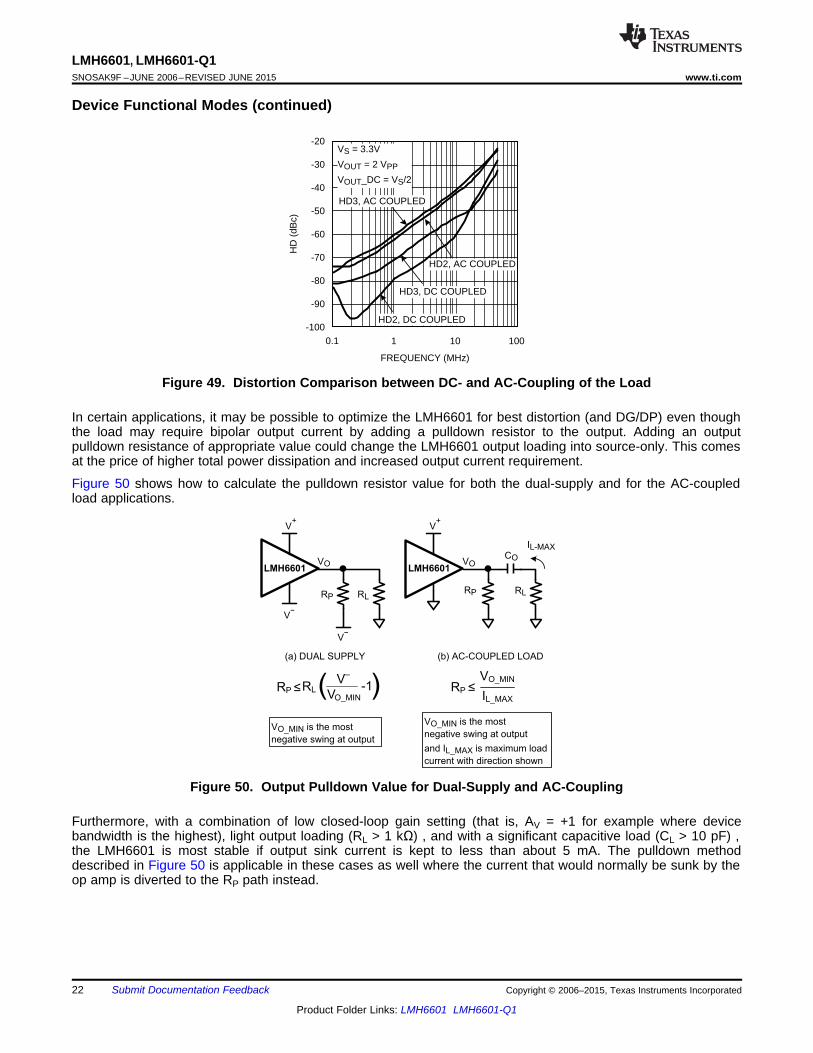
7.3 Device Functional Modes
7.3.1 Optimizing PerformanceWith many op amps, additional device nonlinearity and sometimes less loop stability arises when the output mustswitch from current-source mode to current-sink mode or vice versa. When it comes to achieving the lowestdistortion and the best Differential Gain/ Differential Phase (DG/ DP, broadcast video specs), the LMH6601 isoptimized for single-supply DC-coupled output applications where the load current is returned to the negative rail(V−). That is where the output stage is most linear (lowest distortion) and which corresponds to unipolar currentflowing out of this device. To that effect, it is easy to see that the distortion specifications improve when theoutput is only sourcing current which is the distortion-optimized mode of operation for the LMH6601. In anapplication where the LMH6601 output is AC-coupled or when it is powered by separate dual supplies for V+ andV−, the output stage supplies both source and sink current to the load and results in less than optimum distortion(and DG/DP). Figure 49 compares the distortion results between a DC- and an AC-coupled load to show themagnitude of this difference. See the DG/DP plots, Figure 43 through Figure 46, in Typical Characteristics, for acomparison between DC- and AC-coupling of the video load.
Copyright © 2006–2015, Texas Instruments Incorporated Submit Documentation Feedback 21
Product Folder Links: LMH6601 LMH6601-Q1
V+
RP RL
VO
IL-MAXCO
V+
V-
RP RL
V-
VO
(a) DUAL SUPPLY (b) AC-COUPLED LOAD
( V–
VO_MIN
-1RP ≤RL
VO_MIN
IL_MAX
RP ≤
VO_MIN is the most
negative swing at output
VO_MIN is the most
negative swing at output
and IL_MAX is maximum load
current with direction shown
LMH6601LMH6601
)
0.1 1 10 100
FREQUENCY (MHz)
-100
-90
-80
-70
-60
-50
-40
-30
-20
HD
(dB
c)
VS = 3.3V
VOUT = 2 VPP
VOUT_DC = VS/2
HD2, DC COUPLED
HD3, DC COUPLED
HD2, AC COUPLED
HD3, AC COUPLED
LMH6601, LMH6601-Q1SNOSAK9F –JUNE 2006–REVISED JUNE 2015 www.ti.com
Device Functional Modes (continued)
Figure 49. Distortion Comparison between DC- and AC-Coupling of the Load
In certain applications, it may be possible to optimize the LMH6601 for best distortion (and DG/DP) even thoughthe load may require bipolar output current by adding a pulldown resistor to the output. Adding an outputpulldown resistance of appropriate value could change the LMH6601 output loading into source-only. This comesat the price of higher total power dissipation and increased output current requirement.
Figure 50 shows how to calculate the pulldown resistor value for both the dual-supply and for the AC-coupledload applications.
Figure 50. Output Pulldown Value for Dual-Supply and AC-Coupling
Furthermore, with a combination of low closed-loop gain setting (that is, AV = +1 for example where devicebandwidth is the highest), light output loading (RL > 1 kΩ) , and with a significant capacitive load (CL > 10 pF) ,the LMH6601 is most stable if output sink current is kept to less than about 5 mA. The pulldown methoddescribed in Figure 50 is applicable in these cases as well where the current that would normally be sunk by theop amp is diverted to the RP path instead.
22 Submit Documentation Feedback Copyright © 2006–2015, Texas Instruments Incorporated
Product Folder Links: LMH6601 LMH6601-Q1

+
-
VIDEO IN (0-0.75V)
RT75:
VS = 2.7V
RF620:
RG620:
RS75: RL
75:
VLOADLMH6601
75: CABLE
LMH6601, LMH6601-Q1www.ti.com SNOSAK9F –JUNE 2006–REVISED JUNE 2015
8 Application and Implementation
NOTEInformation in the following applications sections is not part of the TI componentspecification, and TI does not warrant its accuracy or completeness. TI’s customers areresponsible for determining suitability of components for their purposes. Customers shouldvalidate and test their design implementation to confirm system functionality.
8.1 Application Information
8.1.1 DC-Coupled, Single-Supply Baseband Video Amplifier and DriverThe LMH6601 output can swing very close to either rail to maximize the output dynamic range which is ofparticular interest when operating in a low-voltage, single-supply environment. Under light output load conditions,the output can swing as close as a few mV of either rail. This also allows a video amplifier to preserve the videoblack level for excellent video integrity. In the example shown in Figure 51, the baseband video output isamplified and buffered by the LMH6601 which then drives the 75-Ω back-terminated video cable for an overallgain of +1 delivered to the 75-Ω load. The input video would normally have a level between 0 V to approximately0.75 V.
Figure 51. Single-Supply Video Driver Capable of Maintaining Accurate Video Black Level
With the LMH6601 input common-mode range including the V− (ground) rail, there will be no need for AC-coupling or level shifting and the input can directly drive the noninverting input which has the additionaladvantage of high amplifier input impedance. With LMH6601’s wide rail-to-rail output swing, as stated earlier, thevideo black level of 0 V is maintained at the load with minimal circuit complexity and using no AC-couplingcapacitors. Without true rail-to-rail output swing of the LMH6601, and more importantly without the LMH6601’sability of exceedingly close swing to V−, the circuit would not operate properly as shown at the expense of morecomplexity. This circuit will also work for higher input voltages. The only significant requirement is that there is atleast 1.8 V from the maximum input voltage to the positive supply (V+).
The Composite Video Output of some low-cost consumer video equipment consists of a current source whichdevelops the video waveform across a load resistor (usually 75 Ω), as shown in Figure 52. With theseapplications, the same circuit configuration just described and shown in Figure 52 will be able to buffer and drivethe Composite Video waveform which includes sync and video combined. However, with this arrangement, theLMH6601 supply voltage must be at least 3.3 V or higher to allow proper input common-mode voltage headroombecause the input can be as high as 1-V peak.
Copyright © 2006–2015, Texas Instruments Incorporated Submit Documentation Feedback 23
Product Folder Links: LMH6601 LMH6601-Q1

RF
R3=
0.613.3V ± 0.61 = 0.2271 +
RF
RG¨¨
©
§ ¨¨
©
§
1 + RF
¨¨
©
§ ¨¨
©
§RG
-1 = 1.5V/VRF
RG||R3=
2V
0.8V
+
-
VS = 3.3V
RF620:
RG560:
RS75: RL
75:
VLOADLMH6601
U1
0V - 2V
R31.3 k:
3.3V
R130 k:
R210 k:
RT75:
VIDEO IN-0.3V to 0.75V
0.8VPP0.61V ± 1.41V
3.3V
+
-
COMPOSITEVIDEO IN 0-1V
75:
VS = 3.3V
RF620:
RG620:
RS75: RL
75:
VLOADLMH6601
U1iO
VIDEO DAC CURRENT OUTPUT
LMH6601, LMH6601-Q1SNOSAK9F –JUNE 2006–REVISED JUNE 2015 www.ti.com
Application Information (continued)
Figure 52. Single-Supply Composite Video Driver for Consumer Video Outputs
If the Video In signal is Composite Video with negative going Sync tip, a variation of the previous configurationsshould be used. This circuit produces a unipolar (more than 0 V) DC-coupled single-supply video signal asshown in Figure 53.
Figure 53. Single-Supply, DC-Coupled Composite Video Driver for Negative Going Sync Tip
In the circuit of Figure 53, the input is shifted positive by means of R1, R2, and RT in order to satisfy the common-mode input range of the U1. The signal will loose 20% of its amplitude in the process. The closed-loop gain of U1must be set to make up for this 20% loss in amplitude. This gives rise to the gain expression shown inEquation 1, which is based on a getting a 2 VPP output with a 0.8 VPP input:
(1)
R3 will produce a negative shift at the output due to VS (3.3 V in this case). R3 must be set so that the Video Insync tip (−0.3 V at RT or 0.61 V at U1 noninverting input) corresponds to near 0 V at the output.
(2)
Equation 1 and Equation 2 must be solved simultaneously to arrive at the values of R3, RF, and RG which willsatisfy both. From the data sheet, one can set RF = 620 Ω to be close to the recommended value for a gain of+2. It is easier to solve for RG and R3 by starting with a good estimate for one and iteratively solving Equation 1and Equation 2 to arrive at the results. Here is one possible iteration cycle for reference:
RF = 620 Ω (3)
24 Submit Documentation Feedback Copyright © 2006–2015, Texas Instruments Incorporated
Product Folder Links: LMH6601 LMH6601-Q1

-3 dB_BW = 0.35
RISE/FALL_TIME=
0.356.8 ns
= 52 MHz
RISE/FALL_TIME = PIXEL_TIME
3=
20.3 ns
3= 6.8 ns
PIXEL_TIME (ns) = REFRESH_RATE
H x V
1x KH x KV
x 1 x 105
= 75 Hz
800 x 600
1x 76 x 96
x 1 x 105
= 20.3 ns
LMH6601, LMH6601-Q1www.ti.com SNOSAK9F –JUNE 2006–REVISED JUNE 2015
Application Information (continued)Table 1. Finding External Resistor Values by Iteration for Figure 53
ESTIMATE CALCULATED Equation 1 LHS COMMENTRG (Ω) (from Equation 2) CALCULATED (COMPARE Equation 1 LHS calculated to RHS)
R3 (Ω)1k 1.69k 0.988 Increase Equation 1 LHS by reducing RG
820 1.56k 1.15 Increase Equation 1 LHS by reducing RG
620 1.37k 1.45 Increase Equation 1 LHS by reducing RG
390 239 4.18 Reduce Equation 1 LHS by increasing RG
560 1.30k 1.59 Close to target value of 1.5V/V for Equation 1
The final set of values for RG and R3 in Table 1 are values which will result in the proper gain and correct videolevels (0 V to 1 V) at the output (VLOAD).
8.1.2 How to Pick the Right Video AmplifierApart from output current drive and voltage swing, the op amp used for a video amplifier and cable driver shouldalso possess the minimum requirement for speed and slew rate. For video type loads, it is best to consider LargeSignal Bandwidth (or LSBW in the TI data sheet tables) as video signals could be as large as 2 VPP whenapplied to the commonly used gain of +2 configuration. Because of this relatively large swing, the op amp SlewRate (SR) limitation should also be considered. Table 2 shows these requirements for various video line ratescalculated using a rudimentary technique and intended as a first-order estimate only.
Table 2. Rise Time, −3 dB BW, and Slew Rate Requirements for Various Video Line RatesVIDEO LINE RATE REFRESH HORIZONTA VERTICAL PIXEL TIME RISE TIME LSBW SR
STANDARD (HxV) RATE L ACTIVE (ns) (ns) (MHz) (V/μs)(Hz) ACTIVE (KV%)
(KH%)TV_NTSC 451x483 30 84 92 118.3 39.4 9 41
VGA 640x480 75 80 95 33 11 32 146SVGA 800x600 75 76 96 20.3 6.8 52 237XGA 1024x768 75 77 95 12.4 4.1 85 387
SXGA 1280x1024 75 75 96 7.3 2.4 143 655UXGA 1600x1200 75 74 96 4.9 1.6 213 973
For any video line rate (HxV corresponding to the number of Active horizontal and vertical lines), the speedrequirements can be estimated if the Horizontal Active (KH%) and Vertical Active (KV%) numbers are known.These percentages correspond to the percentages of the active number of lines (horizontal or vertical) to the totalnumber of lines as set by VESA standards. Here are the general expressions and the specific calculations for theSVGA line rate shown in Table 2.
(4)
Requiring that an “On” pixel is illuminated to at least 90 percent of its final value before changing state will resultin the rise/fall time equal to, at most, ⅓ the pixel time as shown in Equation 5:
(5)
Assuming a single pole frequency response roll-off characteristic for the closed-loop amplifier used, we have:
(6)
Copyright © 2006–2015, Texas Instruments Incorporated Submit Documentation Feedback 25
Product Folder Links: LMH6601 LMH6601-Q1

0.1 1 10 1000
100
200
300
400
500
600
CA
PA
CIT
AN
CE
(pF
)
REVERSED BIAS VOLTAGE (V)
T = 23°C
PIN-RD100
PIN-RD100A
PIN-RD15
PIN-RD07
+
-D1
VBIAS
CD CA
LMH6601U1
RF
CF
VOUT
SR(V/Ps) = 1.6V
RISE/FALL_TIME (ns)=
1.6V6.8 ns
= 237(V/Ps)x 1 x 10³
LMH6601, LMH6601-Q1SNOSAK9F –JUNE 2006–REVISED JUNE 2015 www.ti.com
Rise/Fall times are 10%-90% transition times, which for a 2 VPP video step would correspond to a total voltageshift of 1.6V (80% of 2 V). So, the Slew Rate requirement can be calculated as follows:
(7)
The LMH6601 specifications show that it would be a suitable choice for video amplifiers up to and including theSVGA line rate as demonstrated above.
For more information about this topic and others relating to video amplifiers, see Application Note 1013, VideoAmplifier Design for Computer Monitors (SNVA031).
8.1.3 Current to Voltage Conversion (Transimpedance Amplifier (TIA)Being capable of high speed and having ultra low input bias current makes the LMH6601 a natural choice forCurrent to Voltage applications such as photodiode I-V conversion. In these type of applications, as shown inFigure 54, the photodiode is tied to the inverting input of the amplifier with RF set to the proper gain (gain ismeasured in Ω).
Figure 54. Typical Connection of a Photodiode Detector to an Op Amp
With the LMH6601 input bias current in the femto-amperes range, even large values of gain (RF) do not increasethe output error term appreciably. This allows circuit operation to a lower light intensity level which is always ofspecial importance in these applications. Most photo-diodes have a relatively large capacitance (CD) which wouldbe even larger for a photo-diode designed for higher sensitivity to light because of its larger area. Someapplications may run the photodiode with a reverse bias to reduce its capacitance with the disadvantage ofincreased contributions from both dark current and noise current. Figure 55 shows a typical photodiodecapacitance plot vs. reverse bias for reference.
Figure 55. Typical Capacitance vs. Reverse Bias (Source: OSI Optoelectronics)
26 Submit Documentation Feedback Copyright © 2006–2015, Texas Instruments Incorporated
Product Folder Links: LMH6601 LMH6601-Q1
2SRFCINf-3 dB
GBWP#
CF = CIN
2S(GBWP)RF
NOISE GAIN (NG)
OP AMP OPEN-
LOOP GAIN
I-V GAIN (Ω)
GA
IN (
dB
)
0 dB
FREQUENCY
1 + sRF (CIN + CF)
1 + sRFCF
1 +CIN
CF
GBWPfz =
1
2 Rπ FCIN
fP =1
2 Rπ FCF
LMH6601, LMH6601-Q1www.ti.com SNOSAK9F –JUNE 2006–REVISED JUNE 2015
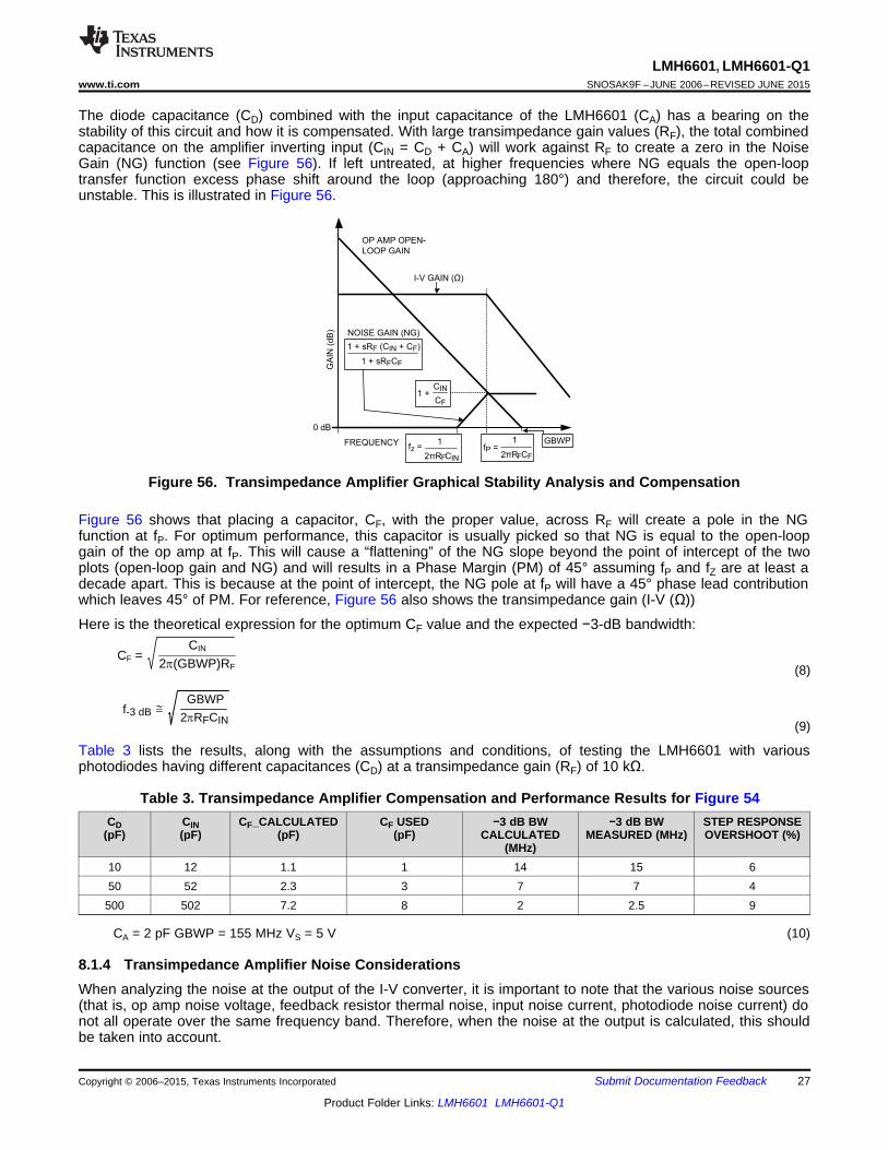
The diode capacitance (CD) combined with the input capacitance of the LMH6601 (CA) has a bearing on thestability of this circuit and how it is compensated. With large transimpedance gain values (RF), the total combinedcapacitance on the amplifier inverting input (CIN = CD + CA) will work against RF to create a zero in the NoiseGain (NG) function (see Figure 56). If left untreated, at higher frequencies where NG equals the open-looptransfer function excess phase shift around the loop (approaching 180°) and therefore, the circuit could beunstable. This is illustrated in Figure 56.
Figure 56. Transimpedance Amplifier Graphical Stability Analysis and Compensation
Figure 56 shows that placing a capacitor, CF, with the proper value, across RF will create a pole in the NGfunction at fP. For optimum performance, this capacitor is usually picked so that NG is equal to the open-loopgain of the op amp at fP. This will cause a “flattening” of the NG slope beyond the point of intercept of the twoplots (open-loop gain and NG) and will results in a Phase Margin (PM) of 45° assuming fP and fZ are at least adecade apart. This is because at the point of intercept, the NG pole at fP will have a 45° phase lead contributionwhich leaves 45° of PM. For reference, Figure 56 also shows the transimpedance gain (I-V (Ω))
Here is the theoretical expression for the optimum CF value and the expected −3-dB bandwidth:
(8)
(9)
Table 3 lists the results, along with the assumptions and conditions, of testing the LMH6601 with variousphotodiodes having different capacitances (CD) at a transimpedance gain (RF) of 10 kΩ.
Table 3. Transimpedance Amplifier Compensation and Performance Results for Figure 54CD CIN CF_CALCULATED CF USED −3 dB BW −3 dB BW STEP RESPONSE
(pF) (pF) (pF) (pF) CALCULATED MEASURED (MHz) OVERSHOOT (%)(MHz)
10 12 1.1 1 14 15 650 52 2.3 3 7 7 4
500 502 7.2 8 2 2.5 9
CA = 2 pF GBWP = 155 MHz VS = 5 V (10)
8.1.4 Transimpedance Amplifier Noise ConsiderationsWhen analyzing the noise at the output of the I-V converter, it is important to note that the various noise sources(that is, op amp noise voltage, feedback resistor thermal noise, input noise current, photodiode noise current) donot all operate over the same frequency band. Therefore, when the noise at the output is calculated, this shouldbe taken into account.
Copyright © 2006–2015, Texas Instruments Incorporated Submit Documentation Feedback 27
Product Folder Links: LMH6601 LMH6601-Q1

-
+
RS
RL2 k:
VOUTLMH6601
U1
RG RF
CF
CL
VIN
+
-LMH6601
U1
RF
CF
VOUT
D1
10 k: RS CD
VBIAS 1000 pF
RF = 10 M: to 10 G:
RS = 1 M: or SMALLER FOR HIGH COUNTING RATES
CF = 1 pF
CD = 1 pF to 10 PF
VOUT = Q/CF WHERE Q is CHARGE CREATED BY ONE PHOTON or PARTICLE
ADJUST VBIAS FOR MAXIMUM SNR
+-
LMH6601, LMH6601-Q1SNOSAK9F –JUNE 2006–REVISED JUNE 2015 www.ti.com
The op amp noise voltage will be gained up in the region between the noise gain’s “zero” and its “pole” (fz and fpin Figure 56). The higher the values of RF and CIN, the sooner the noise gain peaking starts and therefore itscontribution to the total output noise would be larger. It is obvious to note that it is advantageous to minimize CIN(for example, by proper choice of op amp, by applying a reverse bias across the diode at the expense of excessdark current and noise). However, most low noise op amps have a higher input capacitance compared toordinary op amps. This is due to the low noise op amp’s larger input stage.
8.1.5 Charge Preamplifier
Figure 57. Charge Preamplifier Taking Advantage of the Femto-Ampere Range Input Bias Current of theLMH6601
8.1.6 Capacitive LoadThe LMH6601 can drive a capacitive load of up to 1000 pF with correct isolation and compensation. Figure 58illustrates the in-loop compensation technique to drive a large capacitive load.
Figure 58. In-Loop Compensation Circuit for Driving a Heavy Capacitive Load
When driving a high-capacitive load, an isolation resistor (RS) should be connected in series between the op ampoutput and the capacitive load to provide isolation and to avoid oscillations. A small-value capacitor (CF) isinserted between the op amp output and the inverting input as shown such that this capacitor becomes thedominant feedback path at higher frequency. Together these components allow heavy capacitive loading whilekeeping the loop stable.
There are few factors which affect the driving capability of the op amp:• Op amp internal architecture• Closed-loop gain and output capacitor loading
Table 4 shows the measured step response for various values of load capacitors (CL), series resistor (RS) andfeedback resistor (CF) with gain of +2 (RF = RG = 604 Ω) and RL = 2 kΩ:
28 Submit Documentation Feedback Copyright © 2006–2015, Texas Instruments Incorporated
Product Folder Links: LMH6601 LMH6601-Q1

+
-
5V
RF620:
RG620:
RO75:
RL75:
VOUTLMH6601
U1CO
220 PF
CABLEVIN
CG2
CG47 PF
+
5V
CIN0.47 PF
R1510 k:
R2510 k:
+RIN75:
10 100 10000
10
20
30
40
50
60
70R
ISE
TIM
E (
ns)
CAP LOAD CL (pF)
LMH6601, LMH6601-Q1www.ti.com SNOSAK9F –JUNE 2006–REVISED JUNE 2015
Table 4. LMH6601 Step Response Summary for the Circuit of Figure 58CL RS CF trise/ tfall OVERSHOOT
(pF) (Ω) (pF) (ns) (%)10 0 1 6 (1) 850 0 1 7 (1) 6
110 47 1 10 16300 6 10 12 20500 80 10 33 10910 192 10 65 10
(1) Response limited by input step generator rise time of 5 ns
Figure 59 shows the increase in rise/fall time (bandwidth decrease) at VOUT with larger capacitive loads,illustrating the trade-off between the two:
Figure 59. LMH6601 In-Loop Compensation Response
8.2 Typical Application
8.2.1 SAG Compensation for AC-Coupled VideoMany monitors and displays accept AC-coupled inputs. This simplifies the amplification and buffering task insome respects. The capacitors shown in Figure 60 (except CG2), and especially CO, are the large electrolytic typewhich are considerably costly and take up valuable real estate on the board. It is possible to reduce the value ofthe output coupling capacitor, CO, which is the largest of all, by using what is called SAG compensation. SAGrefers to what the output video experiences due to the low frequency video content it contains which cannotadequately go through the output AC-coupling scheme due to the low frequency limit of this circuit. The −3 dBlow frequency limit of the output circuit is given by:
f_low_frequency (−3 dB)= 1/ (2*π* 75*2(Ω) * Co) = ∼ 4.82 Hz for CO = 220 μF (11)
Figure 60. AC-Coupled Video Amplifier and Driver
Copyright © 2006–2015, Texas Instruments Incorporated Submit Documentation Feedback 29
Product Folder Links: LMH6601 LMH6601-Q1
+
-
VCC_5V
RO75:
VLLMH6601
U1
CO68 PF
CABLE
VCC_5V
CIN0.47 PF
R1510 k:
R2510 k:
+ -
+ -
R42 k:
R31 k:C1
22 PF
R5680:
VIN VO
RT75:
RL75:
LMH6601, LMH6601-Q1SNOSAK9F –JUNE 2006–REVISED JUNE 2015 www.ti.com
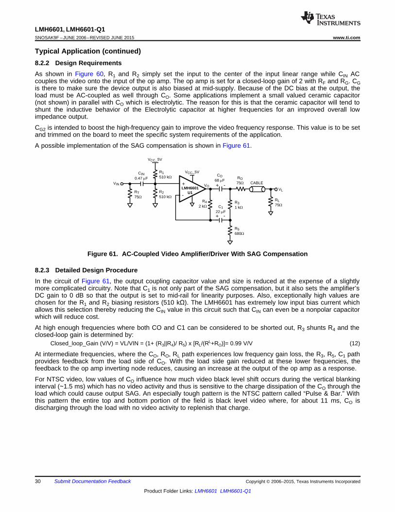
Typical Application (continued)8.2.2 Design RequirementsAs shown in Figure 60, R1 and R2 simply set the input to the center of the input linear range while CIN ACcouples the video onto the input of the op amp. The op amp is set for a closed-loop gain of 2 with RF and RG. CGis there to make sure the device output is also biased at mid-supply. Because of the DC bias at the output, theload must be AC-coupled as well through CO. Some applications implement a small valued ceramic capacitor(not shown) in parallel with CO which is electrolytic. The reason for this is that the ceramic capacitor will tend toshunt the inductive behavior of the Electrolytic capacitor at higher frequencies for an improved overall lowimpedance output.
CG2 is intended to boost the high-frequency gain to improve the video frequency response. This value is to be setand trimmed on the board to meet the specific system requirements of the application.
A possible implementation of the SAG compensation is shown in Figure 61.
Figure 61. AC-Coupled Video Amplifier/Driver With SAG Compensation
8.2.3 Detailed Design ProcedureIn the circuit of Figure 61, the output coupling capacitor value and size is reduced at the expense of a slightlymore complicated circuitry. Note that C1 is not only part of the SAG compensation, but it also sets the amplifier’sDC gain to 0 dB so that the output is set to mid-rail for linearity purposes. Also, exceptionally high values arechosen for the R1 and R2 biasing resistors (510 kΩ). The LMH6601 has extremely low input bias current whichallows this selection thereby reducing the CIN value in this circuit such that CIN can even be a nonpolar capacitorwhich will reduce cost.
At high enough frequencies where both CO and C1 can be considered to be shorted out, R3 shunts R4 and theclosed-loop gain is determined by:
Closed_loop_Gain (V/V) = VL/VIN = (1+ (R3||R4)/ R5) x [RL/(RL+RO)]= 0.99 V/V (12)
At intermediate frequencies, where the CO, RO, RL path experiences low frequency gain loss, the R3, R5, C1 pathprovides feedback from the load side of CO. With the load side gain reduced at these lower frequencies, thefeedback to the op amp inverting node reduces, causing an increase at the output of the op amp as a response.
For NTSC video, low values of CO influence how much video black level shift occurs during the vertical blankinginterval (∼1.5 ms) which has no video activity and thus is sensitive to the charge dissipation of the CO through theload which could cause output SAG. An especially tough pattern is the NTSC pattern called “Pulse & Bar.” Withthis pattern the entire top and bottom portion of the field is black level video where, for about 11 ms, CO isdischarging through the load with no video activity to replenish that charge.
30 Submit Documentation Feedback Copyright © 2006–2015, Texas Instruments Incorporated
Product Folder Links: LMH6601 LMH6601-Q1

2Vp-p
2Vp-p
2Vp-p
(A)50% DUTY CYCLE
NO CLIPPING
(B)LOW DUTY CYCLE
CLIPPED POSITIVE
(C)HIGH DUTY CYCLE
CLIPPED NEGATIVE
4.0V (+) CLIPPING
2.5V
1.0V (-) CLIPPING
4.0V (+) CLIPPING
2.5V
1.0V (-) CLIPPING
4.0V (+) CLIPPING
2.5V
1.0V (-) CLIPPING
LMH6601, LMH6601-Q1www.ti.com SNOSAK9F –JUNE 2006–REVISED JUNE 2015
Typical Application (continued)8.2.4 Application CurvesFigure 62 shows the output of the Figure 61 circuit highlighting the SAG.
Figure 62. AC-Coupled Video Amplifier/Driver Output Scope Photo Showing Video SAG
With the circuit of Figure 61 and any other AC-coupled pulse amplifier, the waveform duty cycle variations exertadditional restrictions on voltage swing at any node. This is illustrated in the waveforms shown in Figure 63.
If a stage has a 3 VPP unclipped swing capability available at a given node, as shown in Figure 63, the maximumallowable amplitude for an arbitrary waveform is ½ of 3 V or 1.5 VPP. This is due to the shift in the average valueof the waveform as the duty cycle varies. Figure 63 shows what would happen if a 2 VPP signal were applied. Alow duty cycle waveform, such as the one in Figure 63B, would have high positive excursions. At low enoughduty cycles, the waveform could get clipped on the top, as shown, or a more subtle loss of linearity could occurprior to full-blown clipping. The converse of this occurs with high duty cycle waveforms and negative clipping, asdepicted in Figure 63C.
Figure 63. Headroom Considerations With AC-Coupled Amplifiers
Copyright © 2006–2015, Texas Instruments Incorporated Submit Documentation Feedback 31
Product Folder Links: LMH6601 LMH6601-Q1

LMH6601, LMH6601-Q1SNOSAK9F –JUNE 2006–REVISED JUNE 2015 www.ti.com
9 Power Supply RecommendationsThe LMH6601 can operate off a single-supply or with dual supplies. The input CM capability of the parts (CMVR)extends all the way down to the V- rail to simplify single-supply applications. Supplies should be decoupled withlow-inductance, often ceramic, capacitors to ground less than 0.5 inches from the device pins. TI recommendsthe use of ground plane, and as in most high-speed devices, it is advisable to remove ground plane close todevice sensitive pins such as the inputs.
10 Layout
10.1 Layout GuidelinesGenerally, a good high-frequency layout will keep power supply and ground traces away from the inverting inputand output pins. Parasitic capacitances on these nodes to ground will cause frequency response peaking andpossible circuit oscillations (see Application Note OA-15, Frequent Faux Pas in Applying Wideband CurrentFeedback Amplifiers, SNOA367, for more information).
10.2 Layout Examples
SC-70 Board Layout (Actual size = 1.5 in × 1.5 in
Figure 64. Layer 1 Silk
SC-70 Board Layout (Actual size = 1.5 in × 1.5 in
Figure 65. Layer 2 Silk
32 Submit Documentation Feedback Copyright © 2006–2015, Texas Instruments Incorporated
Product Folder Links: LMH6601 LMH6601-Q1

LMH6601, LMH6601-Q1www.ti.com SNOSAK9F –JUNE 2006–REVISED JUNE 2015
11 Device and Documentation Support
11.1 Documentation Support
11.1.1 Related DocumentationFor additional information, see the following:• Application Note 1013, Video Amplifier Design for Computer Monitors, SNVA031• Application Note OA-15, Frequent Faux Pas in Applying Wideband Current Feedback Amplifiers, SNOA367
11.2 Related LinksThe table below lists quick access links. Categories include technical documents, support and communityresources, tools and software, and quick access to sample or buy.
Table 5. Related LinksTECHNICAL TOOLS & SUPPORT &PARTS PRODUCT FOLDER SAMPLE & BUY DOCUMENTS SOFTWARE COMMUNITY
LMH6601 Click here Click here Click here Click here Click hereLMH6601-Q1 Click here Click here Click here Click here Click here
11.3 Community ResourcesThe following links connect to TI community resources. Linked contents are provided "AS IS" by the respectivecontributors. They do not constitute TI specifications and do not necessarily reflect TI's views; see TI's Terms ofUse.
TI E2E™ Online Community TI's Engineer-to-Engineer (E2E) Community. Created to foster collaborationamong engineers. At e2e.ti.com, you can ask questions, share knowledge, explore ideas and helpsolve problems with fellow engineers.
Design Support TI's Design Support Quickly find helpful E2E forums along with design support tools andcontact information for technical support.
11.4 TrademarksE2E is a trademark of Texas Instruments.All other trademarks are the property of their respective owners.
11.5 Electrostatic Discharge CautionThese devices have limited built-in ESD protection. The leads should be shorted together or the device placed in conductive foamduring storage or handling to prevent electrostatic damage to the MOS gates.
11.6 GlossarySLYZ022 — TI Glossary.
This glossary lists and explains terms, acronyms, and definitions.
12 Mechanical, Packaging, and Orderable InformationThe following pages include mechanical, packaging, and orderable information. This information is the mostcurrent data available for the designated devices. This data is subject to change without notice and revision ofthis document. For browser-based versions of this data sheet, refer to the left-hand navigation.
Copyright © 2006–2015, Texas Instruments Incorporated Submit Documentation Feedback 33
Product Folder Links: LMH6601 LMH6601-Q1

PACKAGE OPTION ADDENDUM
www.ti.com 11-Sep-2016
Addendum-Page 1
PACKAGING INFORMATION
Orderable Device Status(1)
Package Type PackageDrawing
Pins PackageQty
Eco Plan(2)
Lead/Ball Finish(6)
MSL Peak Temp(3)
Op Temp (°C) Device Marking(4/5)
Samples
LMH6601MG/NOPB ACTIVE SC70 DCK 6 1000 Green (RoHS& no Sb/Br)
CU SN Level-1-260C-UNLIM -40 to 85 A95
LMH6601MGX/NOPB ACTIVE SC70 DCK 6 3000 Green (RoHS& no Sb/Br)
CU SN Level-1-260C-UNLIM -40 to 85 A95
LMH6601QMG/NOPB ACTIVE SC70 DCK 6 1000 Green (RoHS& no Sb/Br)
CU SN Level-1-260C-UNLIM -40 to 85 AKA
(1) The marketing status values are defined as follows:ACTIVE: Product device recommended for new designs.LIFEBUY: TI has announced that the device will be discontinued, and a lifetime-buy period is in effect.NRND: Not recommended for new designs. Device is in production to support existing customers, but TI does not recommend using this part in a new design.PREVIEW: Device has been announced but is not in production. Samples may or may not be available.OBSOLETE: TI has discontinued the production of the device.
(2) Eco Plan - The planned eco-friendly classification: Pb-Free (RoHS), Pb-Free (RoHS Exempt), or Green (RoHS & no Sb/Br) - please check http://www.ti.com/productcontent for the latest availabilityinformation and additional product content details.TBD: The Pb-Free/Green conversion plan has not been defined.Pb-Free (RoHS): TI's terms "Lead-Free" or "Pb-Free" mean semiconductor products that are compatible with the current RoHS requirements for all 6 substances, including the requirement thatlead not exceed 0.1% by weight in homogeneous materials. Where designed to be soldered at high temperatures, TI Pb-Free products are suitable for use in specified lead-free processes.Pb-Free (RoHS Exempt): This component has a RoHS exemption for either 1) lead-based flip-chip solder bumps used between the die and package, or 2) lead-based die adhesive used betweenthe die and leadframe. The component is otherwise considered Pb-Free (RoHS compatible) as defined above.Green (RoHS & no Sb/Br): TI defines "Green" to mean Pb-Free (RoHS compatible), and free of Bromine (Br) and Antimony (Sb) based flame retardants (Br or Sb do not exceed 0.1% by weightin homogeneous material)
(3) MSL, Peak Temp. - The Moisture Sensitivity Level rating according to the JEDEC industry standard classifications, and peak solder temperature.
(4) There may be additional marking, which relates to the logo, the lot trace code information, or the environmental category on the device.
(5) Multiple Device Markings will be inside parentheses. Only one Device Marking contained in parentheses and separated by a "~" will appear on a device. If a line is indented then it is a continuationof the previous line and the two combined represent the entire Device Marking for that device.
(6) Lead/Ball Finish - Orderable Devices may have multiple material finish options. Finish options are separated by a vertical ruled line. Lead/Ball Finish values may wrap to two lines if the finishvalue exceeds the maximum column width.
Important Information and Disclaimer:The information provided on this page represents TI's knowledge and belief as of the date that it is provided. TI bases its knowledge and belief on informationprovided by third parties, and makes no representation or warranty as to the accuracy of such information. Efforts are underway to better integrate information from third parties. TI has taken and

PACKAGE OPTION ADDENDUM
www.ti.com 11-Sep-2016
Addendum-Page 2
continues to take reasonable steps to provide representative and accurate information but may not have conducted destructive testing or chemical analysis on incoming materials and chemicals.TI and TI suppliers consider certain information to be proprietary, and thus CAS numbers and other limited information may not be available for release.
In no event shall TI's liability arising out of such information exceed the total purchase price of the TI part(s) at issue in this document sold by TI to Customer on an annual basis.
OTHER QUALIFIED VERSIONS OF LMH6601, LMH6601-Q1 :
• Catalog: LMH6601
• Automotive: LMH6601-Q1
NOTE: Qualified Version Definitions:
• Catalog - TI's standard catalog product
• Automotive - Q100 devices qualified for high-reliability automotive applications targeting zero defects

TAPE AND REEL INFORMATION
*All dimensions are nominal
Device PackageType
PackageDrawing
Pins SPQ ReelDiameter
(mm)
ReelWidth
W1 (mm)
A0(mm)
B0(mm)
K0(mm)
P1(mm)
W(mm)
Pin1Quadrant
LMH6601MG/NOPB SC70 DCK 6 1000 178.0 8.4 2.25 2.45 1.2 4.0 8.0 Q3
LMH6601MGX/NOPB SC70 DCK 6 3000 178.0 8.4 2.25 2.45 1.2 4.0 8.0 Q3
LMH6601QMG/NOPB SC70 DCK 6 1000 178.0 8.4 2.25 2.45 1.2 4.0 8.0 Q3
PACKAGE MATERIALS INFORMATION
www.ti.com 10-Aug-2016
Pack Materials-Page 1
*All dimensions are nominal
Device Package Type Package Drawing Pins SPQ Length (mm) Width (mm) Height (mm)
LMH6601MG/NOPB SC70 DCK 6 1000 210.0 185.0 35.0
LMH6601MGX/NOPB SC70 DCK 6 3000 210.0 185.0 35.0
LMH6601QMG/NOPB SC70 DCK 6 1000 210.0 185.0 35.0
PACKAGE MATERIALS INFORMATION
www.ti.com 10-Aug-2016
Pack Materials-Page 2


IMPORTANT NOTICE
Texas Instruments Incorporated and its subsidiaries (TI) reserve the right to make corrections, enhancements, improvements and otherchanges to its semiconductor products and services per JESD46, latest issue, and to discontinue any product or service per JESD48, latestissue. Buyers should obtain the latest relevant information before placing orders and should verify that such information is current andcomplete. All semiconductor products (also referred to herein as “components”) are sold subject to TI’s terms and conditions of salesupplied at the time of order acknowledgment.TI warrants performance of its components to the specifications applicable at the time of sale, in accordance with the warranty in TI’s termsand conditions of sale of semiconductor products. Testing and other quality control techniques are used to the extent TI deems necessaryto support this warranty. Except where mandated by applicable law, testing of all parameters of each component is not necessarilyperformed.TI assumes no liability for applications assistance or the design of Buyers’ products. Buyers are responsible for their products andapplications using TI components. To minimize the risks associated with Buyers’ products and applications, Buyers should provideadequate design and operating safeguards.TI does not warrant or represent that any license, either express or implied, is granted under any patent right, copyright, mask work right, orother intellectual property right relating to any combination, machine, or process in which TI components or services are used. Informationpublished by TI regarding third-party products or services does not constitute a license to use such products or services or a warranty orendorsement thereof. Use of such information may require a license from a third party under the patents or other intellectual property of thethird party, or a license from TI under the patents or other intellectual property of TI.Reproduction of significant portions of TI information in TI data books or data sheets is permissible only if reproduction is without alterationand is accompanied by all associated warranties, conditions, limitations, and notices. TI is not responsible or liable for such altereddocumentation. Information of third parties may be subject to additional restrictions.Resale of TI components or services with statements different from or beyond the parameters stated by TI for that component or servicevoids all express and any implied warranties for the associated TI component or service and is an unfair and deceptive business practice.TI is not responsible or liable for any such statements.Buyer acknowledges and agrees that it is solely responsible for compliance with all legal, regulatory and safety-related requirementsconcerning its products, and any use of TI components in its applications, notwithstanding any applications-related information or supportthat may be provided by TI. Buyer represents and agrees that it has all the necessary expertise to create and implement safeguards whichanticipate dangerous consequences of failures, monitor failures and their consequences, lessen the likelihood of failures that might causeharm and take appropriate remedial actions. Buyer will fully indemnify TI and its representatives against any damages arising out of the useof any TI components in safety-critical applications.In some cases, TI components may be promoted specifically to facilitate safety-related applications. With such components, TI’s goal is tohelp enable customers to design and create their own end-product solutions that meet applicable functional safety standards andrequirements. Nonetheless, such components are subject to these terms.No TI components are authorized for use in FDA Class III (or similar life-critical medical equipment) unless authorized officers of the partieshave executed a special agreement specifically governing such use.Only those TI components which TI has specifically designated as military grade or “enhanced plastic” are designed and intended for use inmilitary/aerospace applications or environments. Buyer acknowledges and agrees that any military or aerospace use of TI componentswhich have not been so designated is solely at the Buyer's risk, and that Buyer is solely responsible for compliance with all legal andregulatory requirements in connection with such use.TI has specifically designated certain components as meeting ISO/TS16949 requirements, mainly for automotive use. In any case of use ofnon-designated products, TI will not be responsible for any failure to meet ISO/TS16949.
Products ApplicationsAudio www.ti.com/audio Automotive and Transportation www.ti.com/automotiveAmplifiers amplifier.ti.com Communications and Telecom www.ti.com/communicationsData Converters dataconverter.ti.com Computers and Peripherals www.ti.com/computersDLP® Products www.dlp.com Consumer Electronics www.ti.com/consumer-appsDSP dsp.ti.com Energy and Lighting www.ti.com/energyClocks and Timers www.ti.com/clocks Industrial www.ti.com/industrialInterface interface.ti.com Medical www.ti.com/medicalLogic logic.ti.com Security www.ti.com/securityPower Mgmt power.ti.com Space, Avionics and Defense www.ti.com/space-avionics-defenseMicrocontrollers microcontroller.ti.com Video and Imaging www.ti.com/videoRFID www.ti-rfid.comOMAP Applications Processors www.ti.com/omap TI E2E Community e2e.ti.comWireless Connectivity www.ti.com/wirelessconnectivity
Mailing Address: Texas Instruments, Post Office Box 655303, Dallas, Texas 75265Copyright © 2016, Texas Instruments Incorporated