LMH6586 32x16 Video Crosspoint Switch (Rev. D) - TI.com · LMH6586 SNCS105D – JULY 2008–...
33
LMH6586 www.ti.com SNCS105D – JULY 2008 – REVISED MARCH 2013 LMH6586 32x16 Video Crosspoint Switch Check for Samples: LMH6586 1FEATURES DESCRIPTION 2• 32 Inputs and 16 Outputs The LMH6586 is a non-blocking analog video • AC-Coupled Inputs with Integrated DC Restore crosspoint switch designed for routing standard Clamp NTSC or PAL composite video signals. The non- • Individually Addressable Outputs blocking architecture allows any of the 32 inputs to be connected to any of the 16 outputs, including any • Pin-Selectable Output Buffer Gain (1 V/V or 2 input that is already connected. Each input has an V/V) integrated DC restore clamp for biasing of the AC- • –3 dB Bandwidth = 66 MHz coupled video signal. The output buffers have a • DG = 0.05%, DP = 0.05° @ R L = 150Ω,A V = 2V/V common selectable gain setting of 1X or 2X and can drive loads of 150Ω. • −70 dB Off-Isolation @ 6 MHz • Individual Input and Output Shutdown Modes The LMH6586 features two types of input signal detection for convenient monitoring of activity on any • Device Power Down Mode input channel. Video detection can be configured to • Video Detection with Programmable Threshold indicate when either “presence of video” or “loss of (8 Levels) video” is detected across the video threshold level • Sync Detection with Pin-Configurable controlled by a programmable register. Additionally, sync detection can be configured to indicate when Threshold “loss of sync” is detected across the sync threshold • 100 kHz I 2 C Interface with 2-Bit Configurable level controlled by a DC voltage input. Slave Address The switch configuration and other parameters are • Single 5V Supply Operation programmable via the I 2 C bus interface. The slave • Extra Video Output (VOUT_16) for External device address is configurable via two external pins Video Sync Separator allowing up to four LMH6586 devices, each with a unique address, on a common I 2 C bus. This helps APPLICATIONS facilitate expansion of the crosspoint matrix array size (e.g. 64 x 16). The LMH6586 operates from a • CCTV Security and Surveillance Systems common single 5V supply for its analog sections as • Analog Video Routing well as its control logic and I 2 C interface. The LMH6586 is offered in a space-saving 80-pin TQFP. 1 Please be aware that an important notice concerning availability, standard warranty, and use in critical applications of Texas Instruments semiconductor products and disclaimers thereto appears at the end of this data sheet. 2All trademarks are the property of their respective owners. PRODUCTION DATA information is current as of publication date. Copyright © 2008–2013, Texas Instruments Incorporated Products conform to specifications per the terms of the Texas Instruments standard warranty. Production processing does not necessarily include testing of all parameters.
Transcript of LMH6586 32x16 Video Crosspoint Switch (Rev. D) - TI.com · LMH6586 SNCS105D – JULY 2008–...
LMH6586
www.ti.com SNCS105D –JULY 2008–REVISED MARCH 2013
LMH6586 32x16 Video Crosspoint SwitchCheck for Samples: LMH6586
1FEATURESDESCRIPTION
2• 32 Inputs and 16 OutputsThe LMH6586 is a non-blocking analog video• AC-Coupled Inputs with Integrated DC Restorecrosspoint switch designed for routing standard
Clamp NTSC or PAL composite video signals. The non-• Individually Addressable Outputs blocking architecture allows any of the 32 inputs to be
connected to any of the 16 outputs, including any• Pin-Selectable Output Buffer Gain (1 V/V or 2input that is already connected. Each input has anV/V)integrated DC restore clamp for biasing of the AC-
• –3 dB Bandwidth = 66 MHz coupled video signal. The output buffers have a• DG = 0.05%, DP = 0.05° @ RL = 150Ω, AV = 2V/V common selectable gain setting of 1X or 2X and can
drive loads of 150Ω.• −70 dB Off-Isolation @ 6 MHz• Individual Input and Output Shutdown Modes The LMH6586 features two types of input signal
detection for convenient monitoring of activity on any• Device Power Down Modeinput channel. Video detection can be configured to
• Video Detection with Programmable Threshold indicate when either “presence of video” or “loss of(8 Levels) video” is detected across the video threshold level
• Sync Detection with Pin-Configurable controlled by a programmable register. Additionally,sync detection can be configured to indicate whenThreshold“loss of sync” is detected across the sync threshold• 100 kHz I2C Interface with 2-Bit Configurablelevel controlled by a DC voltage input.Slave AddressThe switch configuration and other parameters are• Single 5V Supply Operationprogrammable via the I2C bus interface. The slave
• Extra Video Output (VOUT_16) for External device address is configurable via two external pinsVideo Sync Separator allowing up to four LMH6586 devices, each with a
unique address, on a common I2C bus. This helpsAPPLICATIONS facilitate expansion of the crosspoint matrix array size
(e.g. 64 x 16). The LMH6586 operates from a• CCTV Security and Surveillance Systemscommon single 5V supply for its analog sections as
• Analog Video Routing well as its control logic and I2C interface. TheLMH6586 is offered in a space-saving 80-pin TQFP.
1
Please be aware that an important notice concerning availability, standard warranty, and use in critical applications ofTexas Instruments semiconductor products and disclaimers thereto appears at the end of this data sheet.
2All trademarks are the property of their respective owners.
PRODUCTION DATA information is current as of publication date. Copyright © 2008–2013, Texas Instruments IncorporatedProducts conform to specifications per the terms of the TexasInstruments standard warranty. Production processing does notnecessarily include testing of all parameters.

OPTIONAL FUNCTION
75:75:
LMH658632 X 16 VIDEO
CROSSPOINT SWITCH
LMH1980SYNC SEPARATOR
VO
UT
_16
VO
UT
_15
VO
UT
_0
0.1 PF
RE
SE
T
FLA
G
SC
LS
DA
AD
DR
[1]
AD
DR
[0]
PW
DN
MICROCONTROLLER
R_E
XT
0.1 PF
5V
VR
EF
_CLA
MP
x xxx
x
10k
x xxx
x
GA
IN_S
EL
5V
VDD
GND
SYNCOUTPUTS
0.1 PF
VB
IAS
2
5V
DVDD
DVSS
75:
5V
xxxx
xxxxxxx
xxx
xxxxxx
VIN_160.1 PF
75:
5V
xxxx
xxxxxxx
xxx
xxxxxx VIN_31
0.1 PF
75:
5V
VIN_15
0.1 PF
VIN_0
75:
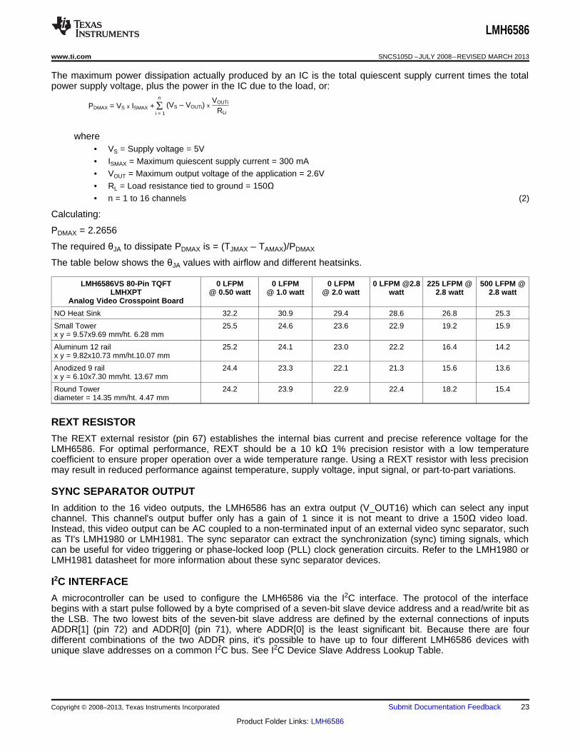
5V
0.1 PF
VB
IAS
1
VR
EF
_SY
NC
0.1 PF
5V
0.1 PF
xxxx
xxxxxxx
xxx
xxxxxx
xxxx
xxxxxxx
xxx
xxxxxx
LMH6586
SNCS105D –JULY 2008–REVISED MARCH 2013 www.ti.com
Application Diagram
2 Submit Documentation Feedback Copyright © 2008–2013, Texas Instruments Incorporated
Product Folder Links: LMH6586
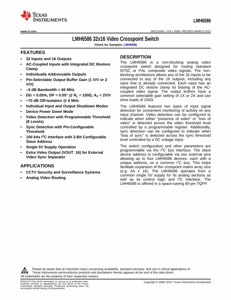
LMH6586
32 COMPARATORS
1X
OUTPUTPOWERSAVE
I2C
BLOCK
VIDEODETECTDAC
DC RESTORE CLAMP
INPUTPOWERSAVE
+
+
32 INPUTS 16 OUTPUTS
INTERNAL BLOCK DIAGRAM
FROM I2C BLOCK
VREF_SYNC
VREF_CLAMP
SDA FLAG
TO I2C BLOCK
FROM I2C BLOCK
TO I2C BLOCK
FROM I2C BLOCK
32 VIDEOINPUTS
SCL
1X
32 x 16SWITCHMATRIX
1X/2X
VOUT 15
VOUT 0
VOUT 16
16 OUTPUTS
0.1 PF
0.1 PFVIN_0
VIN_31
RESET PWDN
VOUT 16
1X/2X
1X
VOUT 15
VOUT 0
ADDR [1]ADDR [0]
VIN 31
VIN 0
GAIN_SEL
1632
32 BLOCKS
32 BLOCKS
TO SYNC SEPARATOR (OPTIONAL)
75:
75:
LMH6586
www.ti.com SNCS105D –JULY 2008–REVISED MARCH 2013
Functional Diagram
Figure 1. Functional Diagram
Copyright © 2008–2013, Texas Instruments Incorporated Submit Documentation Feedback 3
Product Folder Links: LMH6586
VIN_31
VIN_28
VDD
VIN_13
VIN_27
VIN_24
GND
GA
IN_S
EL
VIN_26
VIN_25
RE
SE
T
VIN_14
VIN_29
GND
VIN_15
VIN_8
DV
SS
LMH6586
VO
UT
_5
VO
UT
_3
VO
UT
_4
VO
UT
_6
VIN_4
VIN_1
PW
DN
VIN_30
VIN_23
VIN_22
VIN_20
VIN_21
VIN_19
VIN_18
VIN_17
VIN_16
VDD
GND
VD
D
GN
D
FLA
G
DV
DD
SC
L
SD
A
GN
D
VB
IAS
1
VO
UT
_14
VO
UT
_16
VO
UT
_15
VO
UT
_12
VO
UT
_13
VO
UT
_11
VO
UT
_10
VO
UT
_8
VO
UT
_2
VO
UT
_1
VDD
VIN_0
VIN_2
VIN_3
VIN_7
VIN_6
VIN_10
VIN_11
VIN_12
VD
D
VR
EF
_CLA
MP
VB
IAS
2
VR
EF
_SY
NC
R_E
XT
GN
D
VD
D
VO
UT
_7
AD
DR
[0]
VIN_5
VIN_9
VO
UT
_0
GND
VDDG
ND
VO
UT
_9
1
2
3
4
5
6
7
8
9
10
11
12
13
14
15
16
17
18
19
20
21 22 23 24 25 26 27 28 29 30 31 32 33 34 35 36 37 38 39 40
41
42
43
44
45
46
47
48
49
50
51
52
53
54
55
56
57
58
59
60
61626364656667686970717273747580 79 78 77 76
AD
DR
[1]
VD
D
LMH6586
SNCS105D –JULY 2008–REVISED MARCH 2013 www.ti.com
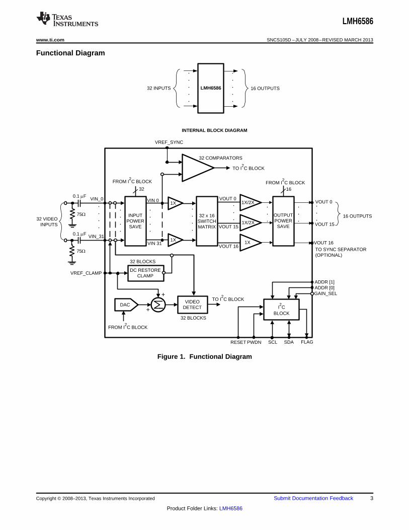
Connection Diagram
4 Submit Documentation Feedback Copyright © 2008–2013, Texas Instruments Incorporated
Product Folder Links: LMH6586
LMH6586
www.ti.com SNCS105D –JULY 2008–REVISED MARCH 2013
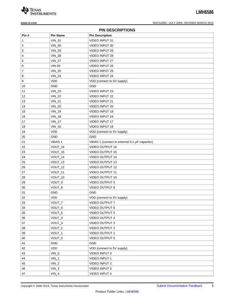
PIN DESCRIPTIONSPin # Pin Name Pin Description
1 VIN_31 VIDEO INPUT 31
2 VIN_30 VIDEO INPUT 30
3 VIN_29 VIDEO INPUT 29
4 VIN_28 VIDEO INPUT 28
5 VIN_27 VIDEO INPUT 27
6 VIN-26 VIDEO INPUT 26
7 VIN_25 VIDEO INPUT 25
8 VIN_24 VIDEO INPUT 24
9 VDD VDD (connect to 5V supply)
10 GND GND
11 VIN_23 VIDEO INPUT 23
12 VIN_22 VIDEO INPUT 22
13 VIN_21 VIDEO INPUT 21
14 VIN_20 VIDEO INPUT 20
15 VIN_19 VIDEO INPUT 19
16 VIN_18 VIDEO INPUT 18
17 VIN_17 VIDEO INPUT 17
18 VIN_16 VIDEO INPUT 16
19 VDD VDD (connect to 5V supply)
20 GND GND
21 VBIAS 1 VBIAS 1 (connect to external 0.1 µF capacitor)
22 VOUT_16 VIDEO OUTPUT 16
23 VOUT_15 VIDEO OUTPUT 15
24 VOUT_14 VIDEO OUTPUT 14
25 VOUT_13 VIDEO OUTPUT 13
26 VOUT_12 VIDEO OUTPUT 12
27 VOUT_11 VIDEO OUTPUT 11
28 VOUT_10 VIDEO OUTPUT 10
29 VOUT_9 VIDEO OUTPUT 9
30 VOUT_8 VIDEO OUTPUT 8
31 GND GND
32 VDD VDD (connect to 5V supply)
33 VOUT_7 VIDEO OUTPUT 7
34 VOUT_6 VIDEO OUTPUT 6
35 VOUT_5 VIDEO OUTPUT 5
36 VOUT_4 VIDEO OUTPUT 4
37 VOUT_3 VIDEO OUTPUT 3
38 VOUT_2 VIDEO OUTPUT 2
39 VOUT_1 VIDEO OUTPUT 1
40 VOUT_0 VIDEO OUTPUT 0
41 GND GND
42 VDD VDD (connect to 5V supply)
43 VIN_0 VIDEO INPUT 0
44 VIN_1 VIDEO INPUT 1
45 VIN_2 VIDEO INPUT 2
46 VIN_3 VIDEO INPUT 3
47 VIN_4 VIDEO INPUT 4
Copyright © 2008–2013, Texas Instruments Incorporated Submit Documentation Feedback 5
Product Folder Links: LMH6586
LMH6586
SNCS105D –JULY 2008–REVISED MARCH 2013 www.ti.com
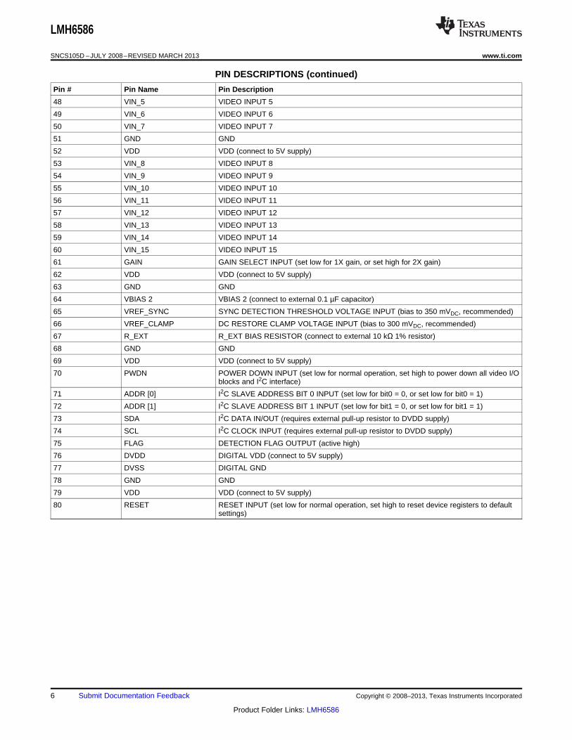
PIN DESCRIPTIONS (continued)
Pin # Pin Name Pin Description
48 VIN_5 VIDEO INPUT 5
49 VIN_6 VIDEO INPUT 6
50 VIN_7 VIDEO INPUT 7
51 GND GND
52 VDD VDD (connect to 5V supply)
53 VIN_8 VIDEO INPUT 8
54 VIN_9 VIDEO INPUT 9
55 VIN_10 VIDEO INPUT 10
56 VIN_11 VIDEO INPUT 11
57 VIN_12 VIDEO INPUT 12
58 VIN_13 VIDEO INPUT 13
59 VIN_14 VIDEO INPUT 14
60 VIN_15 VIDEO INPUT 15
61 GAIN GAIN SELECT INPUT (set low for 1X gain, or set high for 2X gain)
62 VDD VDD (connect to 5V supply)
63 GND GND
64 VBIAS 2 VBIAS 2 (connect to external 0.1 µF capacitor)
65 VREF_SYNC SYNC DETECTION THRESHOLD VOLTAGE INPUT (bias to 350 mVDC, recommended)
66 VREF_CLAMP DC RESTORE CLAMP VOLTAGE INPUT (bias to 300 mVDC, recommended)
67 R_EXT R_EXT BIAS RESISTOR (connect to external 10 kΩ 1% resistor)
68 GND GND
69 VDD VDD (connect to 5V supply)
70 PWDN POWER DOWN INPUT (set low for normal operation, set high to power down all video I/Oblocks and I2C interface)
71 ADDR [0] I2C SLAVE ADDRESS BIT 0 INPUT (set low for bit0 = 0, or set low for bit0 = 1)
72 ADDR [1] I2C SLAVE ADDRESS BIT 1 INPUT (set low for bit1 = 0, or set low for bit1 = 1)
73 SDA I2C DATA IN/OUT (requires external pull-up resistor to DVDD supply)
74 SCL I2C CLOCK INPUT (requires external pull-up resistor to DVDD supply)
75 FLAG DETECTION FLAG OUTPUT (active high)
76 DVDD DIGITAL VDD (connect to 5V supply)
77 DVSS DIGITAL GND
78 GND GND
79 VDD VDD (connect to 5V supply)
80 RESET RESET INPUT (set low for normal operation, set high to reset device registers to defaultsettings)
6 Submit Documentation Feedback Copyright © 2008–2013, Texas Instruments Incorporated
Product Folder Links: LMH6586

LMH6586
www.ti.com SNCS105D –JULY 2008–REVISED MARCH 2013
These devices have limited built-in ESD protection. The leads should be shorted together or the device placed in conductive foamduring storage or handling to prevent electrostatic damage to the MOS gates.
Absolute Maximum Ratings (1) (2)
ESD Tolerance (3) Human Body Model 2500V
Machine Model 250V
Supply Voltage (VDD) 5V
Video Input Voltage Range, VIN −0.3V to VDD +0.3V
Storage Temperature Range −65°C to +150°C
Lead Temperature (Soldering, 10 sec) 300°C
Junction Temperature +150°C
(1) Absolute Maximum Ratings indicate limits beyond which damage to the device may occur. Operating Ratings indicate conditions forwhich the device is intended to be functional, but specific performance is not ensured. For ensured specifications, see the ElectricalCharacteristics tables.
(2) If Military/Aerospace specified devices are required, please contact the Texas Instruments Sales Office/ Distributors for availability andspecifications.
(3) Human Body Model, applicable std. MIL-STD-883, Method 3015.7. Machine Model, applicable std. JESD22-A115-A (ESD MM std. ofJEDEC)Field-Induced Charge-Device Model, applicable std. JESD22-C101-C (ESD FICDM std. of JEDEC).
Operating Ratings (1) (2)
Supply Voltage (VDD) 5V ± 10%
Ambient Temperature Range −40°C ≤ TA ≤ 85°C
θJA 25°C/W
(1) Absolute Maximum Ratings indicate limits beyond which damage to the device may occur. Operating Ratings indicate conditions forwhich the device is intended to be functional, but specific performance is not ensured. For ensured specifications, see the ElectricalCharacteristics tables.
(2) The maximum power dissipation is a function of TJ(MAX) and θJA. The maximum allowable power dissipation at any ambient temperatureis PD = (TJ(MAX) – TA)/ θJA. All numbers apply for packages soldered directly onto a PC Board.
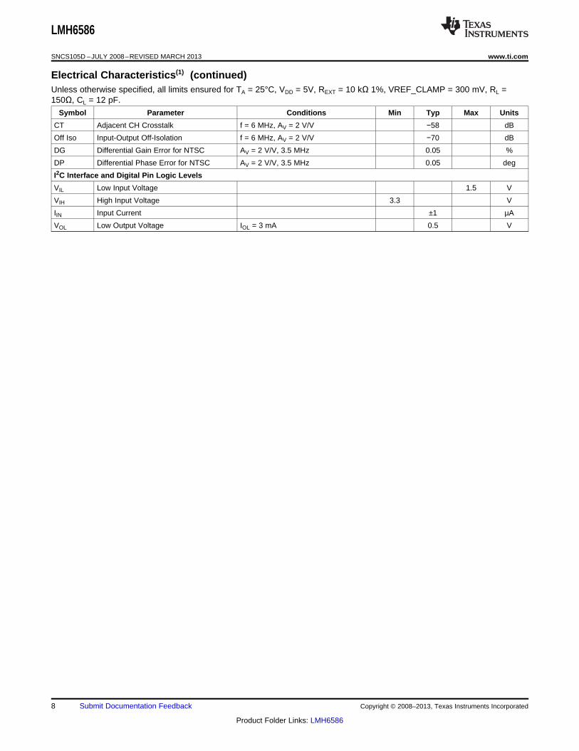
Electrical Characteristics (1)
Unless otherwise specified, all limits ensured for TA = 25°C, VDD = 5V, REXT = 10 kΩ 1%, VREF_CLAMP = 300 mV, RL =150Ω, CL = 12 pF.
Symbol Parameter Conditions Min Typ Max Units
DC Specifications
VDD Operating Supply Voltage 4.5 5.5 V
IDD Supply Current No Load, AV = 1 V/V 300 360 mA
Power Save Supply Current No Load, AV = 1 V/V, SCL= SDA= 1.5 mAPWDN= DVDD
AV Gain 2x Gain Buffer 1.92 2.00 2.07V/V
1x Gain Buffer 0.95 0.99 1.03
ΔAV_CH-CH Gain Matching (Ch to Ch) AV = 1 V/V 1.2 3 %
VOS Output Offset Voltage AV = 1 V/V, No Load (referenced to DC 60 mVrestored input)
VDET_LSB Video Detection Threshold LSB 85 95 105 mV
VDET Video Detection Threshold Offset Video detection threshold offset ±50 mVmeasured above sync tip level of DCrestored input
AC Specifications
BWSS Small Signal Bandwidth (−3 dB) VOUT = 20 mVPP 66 MHz
BWLS Large Signal Bandwidth (−3 dB) VOUT = 1.5 VPP 29 MHz
tr/tf Rise/Fall Time 10% to 90%, VOUT = 2 VPP 35 ns
tp Propagation Delay 50% to 50%, VOUT = 2 VPP 5 ns
tpCh-Ch Ch-Ch Propagation Delay 50% to 50%, VOUT = 2 VPP 5 ns
(1) All voltages are measured with respect to GND, unless otherwise specified.
Copyright © 2008–2013, Texas Instruments Incorporated Submit Documentation Feedback 7
Product Folder Links: LMH6586
LMH6586
SNCS105D –JULY 2008–REVISED MARCH 2013 www.ti.com
Electrical Characteristics(1) (continued)Unless otherwise specified, all limits ensured for TA = 25°C, VDD = 5V, REXT = 10 kΩ 1%, VREF_CLAMP = 300 mV, RL =150Ω, CL = 12 pF.
Symbol Parameter Conditions Min Typ Max Units
CT Adjacent CH Crosstalk f = 6 MHz, AV = 2 V/V −58 dB
Off Iso Input-Output Off-Isolation f = 6 MHz, AV = 2 V/V −70 dB
DG Differential Gain Error for NTSC AV = 2 V/V, 3.5 MHz 0.05 %
DP Differential Phase Error for NTSC AV = 2 V/V, 3.5 MHz 0.05 deg
I2C Interface and Digital Pin Logic Levels
VIL Low Input Voltage 1.5 V
VIH High Input Voltage 3.3 V
IIN Input Current ±1 µA
VOL Low Output Voltage IOL = 3 mA 0.5 V
8 Submit Documentation Feedback Copyright © 2008–2013, Texas Instruments Incorporated
Product Folder Links: LMH6586
OTHER_INPUTS
VSS
VDD
VSS
VIDEO_SYNC_DETECT
VDD
VSS
CROSSPOINT_OUTPUT
SDA
VSS VSS
SCL
VIDEO INPUT CIRCUIT DIAGRAM
OTHER INPUT CIRCUIT DIAGRAM
VIDEO OUTPUT CIRCUIT DIAGRAM VIDEO SYNC DETECT CIRCUIT DIAGRAM
I2C DATA CIRCUIT DIAGRAM I
2C CLOCK CIRCUIT DIAGRAM
VIDEO_INPUT
VDD
VSS
LMH6586
www.ti.com SNCS105D –JULY 2008–REVISED MARCH 2013
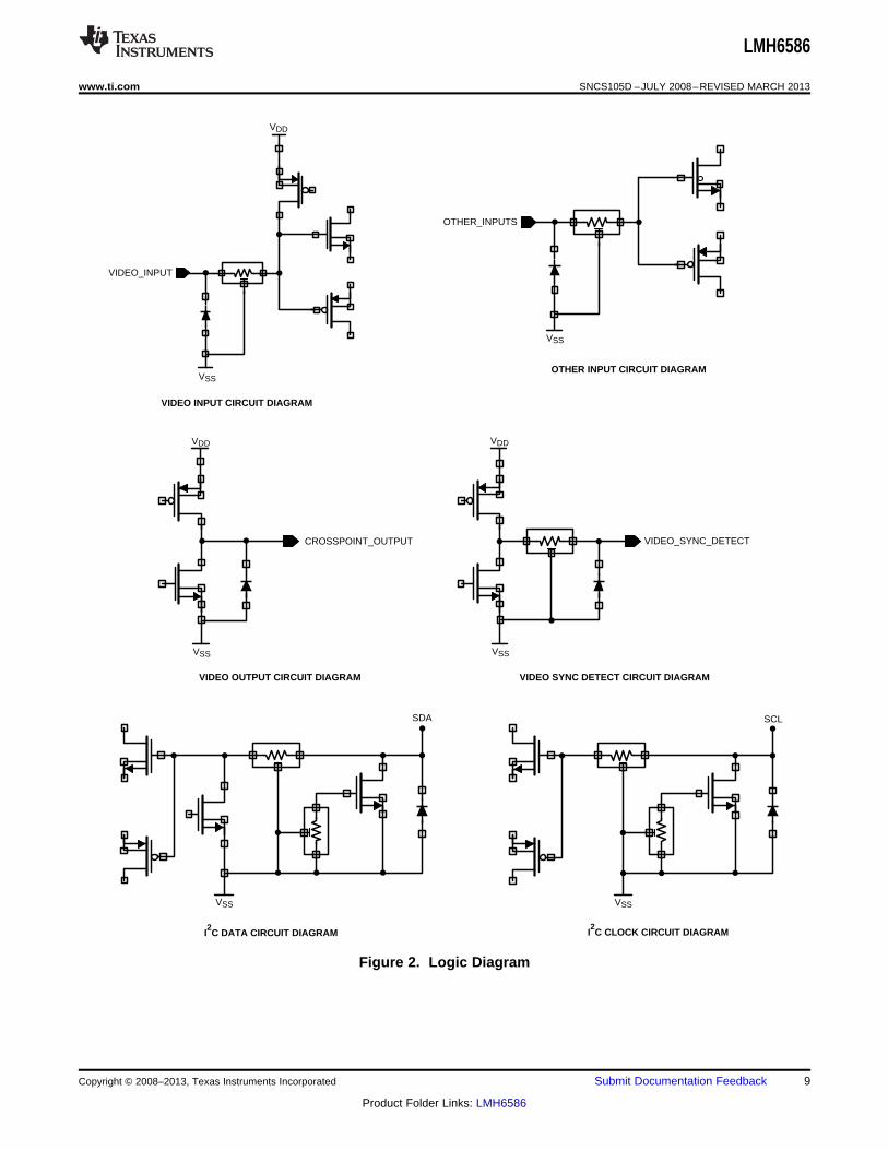
Figure 2. Logic Diagram
Copyright © 2008–2013, Texas Instruments Incorporated Submit Documentation Feedback 9
Product Folder Links: LMH6586
10k 100k 1M 10M 100M-23
-19
-15
-11
-7
-3
1
GA
IN (
dB)
FREQUENCY (Hz)
AV = 1V/V
RL = 150:
10k 100k 1M 10M 100M-12
-10
-8
-6
-4
-2
0
2
4
6
8
GA
IN (
dB)
FREQUENCY (Hz)
AV = 2V/V
RL = 150:
10k 100k 1M 10M 100M-6
-4
-2
0
2
4
6
8
GA
IN (
dB)
FREQUENCY (Hz)
AV = 2V/V
RL = 150:
10k 100k 1M 10M 100M
FREQUENCY (Hz)
-16
-14
-12
-10
-8
-6
-4
-2
0
2
4
GA
IN (
dB)
AV = 1V/V
RL = 150:
10k 100k 1M 10M 100M-6
-4
-2
0
2
4
6
8
GA
IN (
dB)
FREQUENCY (Hz)
AV = 2V/V
RL = 150:
10k 100k 1M 10M 100M-16
-14
-12
-10
-8
-6
-4
-2
0
2
4
GA
IN (
dB)
FREQUENCY (Hz)
AV = 1V/V
RL = 150:
LMH6586
SNCS105D –JULY 2008–REVISED MARCH 2013 www.ti.com
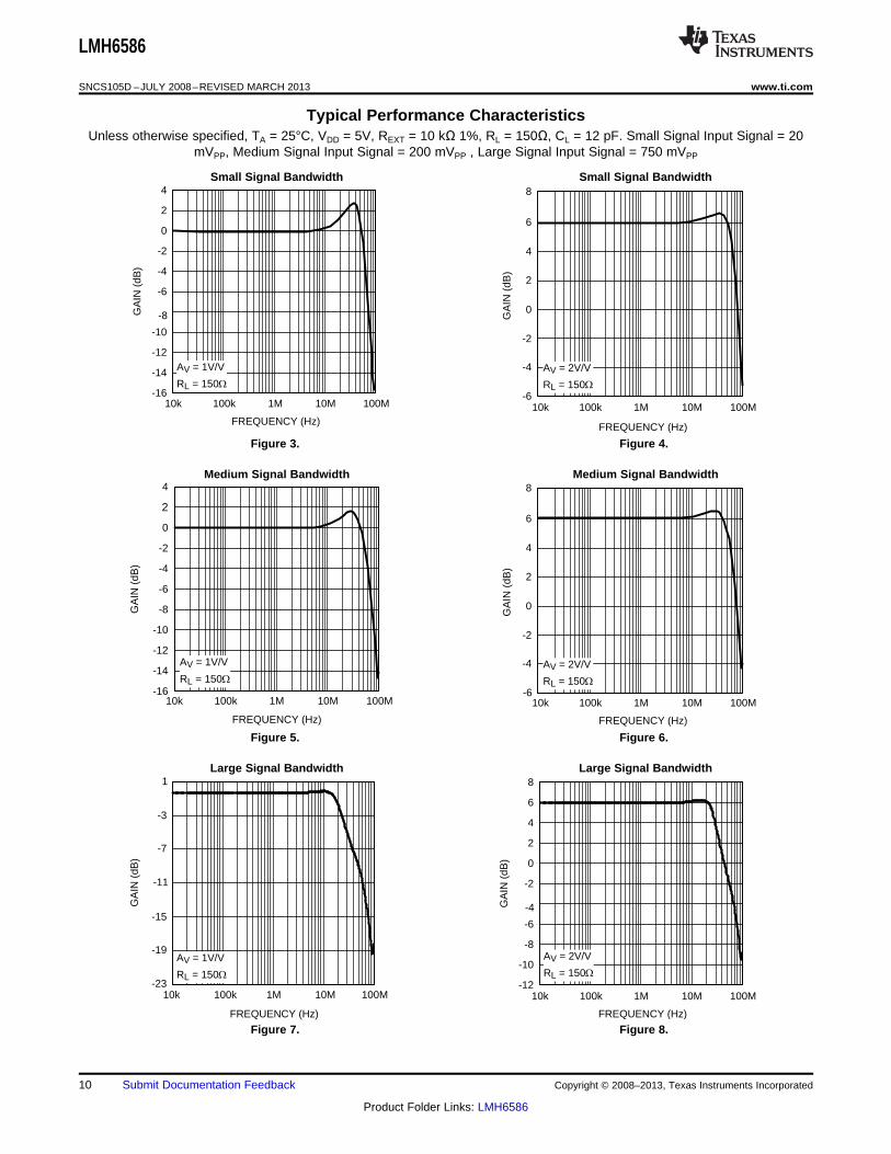
Typical Performance CharacteristicsUnless otherwise specified, TA = 25°C, VDD = 5V, REXT = 10 kΩ 1%, RL = 150Ω, CL = 12 pF. Small Signal Input Signal = 20
mVPP, Medium Signal Input Signal = 200 mVPP , Large Signal Input Signal = 750 mVPP
Small Signal Bandwidth Small Signal Bandwidth
Figure 3. Figure 4.
Medium Signal Bandwidth Medium Signal Bandwidth
Figure 5. Figure 6.
Large Signal Bandwidth Large Signal Bandwidth
Figure 7. Figure 8.
10 Submit Documentation Feedback Copyright © 2008–2013, Texas Instruments Incorporated
Product Folder Links: LMH6586
10k 100k 1M-0.15
-0.1
-0.05
0
0.05
GA
IN (
dB)
FREQUENCY (Hz)
AV = 1V/V
RL = 150:
10k 100k 1M5.85
5.9
5.95
6
6.05
GA
IN (
dB)
FREQUENCY (Hz)
AV = 2V/V
RL = 150:
10k 100k 1M 10M 100M5.6
5.8
6
6.2
6.4
6.6G
AIN
(dB
)
FREQUENCY (Hz)
6.8AV = 2V/V
RL = 150:
10k 100k 1M 10M 100M-2
-1.5
-1
-0.5
0
0.5
1
1.5
2
2.5
3
GA
IN (
dB)
FREQUENCY (Hz)
AV = 1V/V
RL = 150:
10k 100k 1M-0.3
-0.25
-0.2
-0.15
-0.1
-0.05
0
0.05
0.1
FREQUENCY (Hz)
AV = 1V/V
RL = 150:
GA
IN (
dB)
10k 100k 1M5.75
5.8
5.85
5.9
5.95
6
6.05
6.1
GA
IN (
dB)
FREQUENCY (Hz)
AV = 2V/V
RL = 150:
LMH6586
www.ti.com SNCS105D –JULY 2008–REVISED MARCH 2013
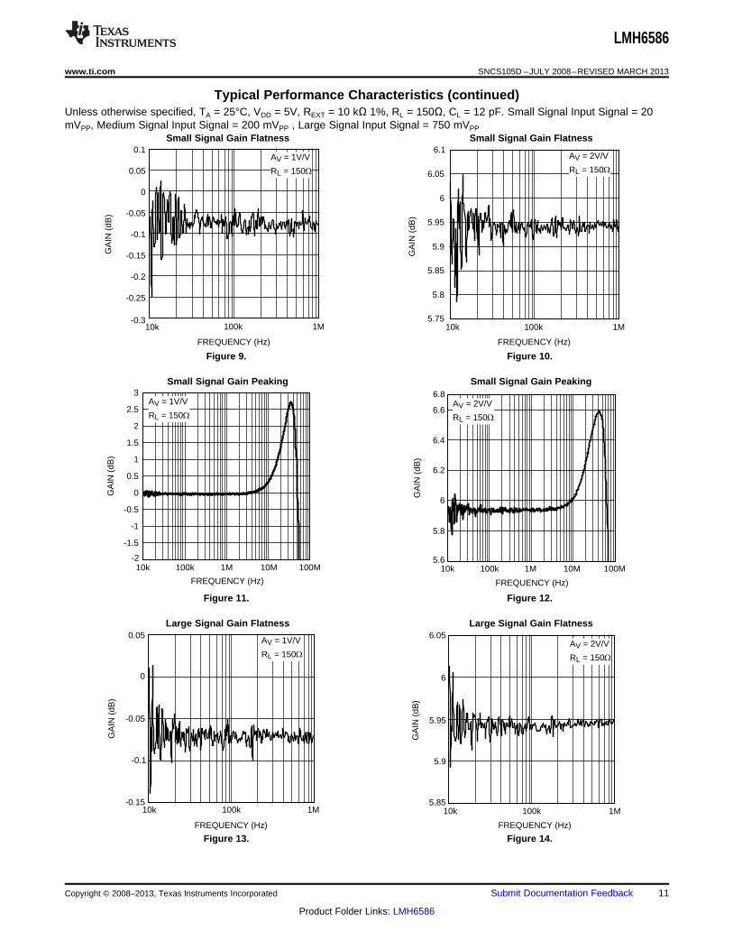
Typical Performance Characteristics (continued)Unless otherwise specified, TA = 25°C, VDD = 5V, REXT = 10 kΩ 1%, RL = 150Ω, CL = 12 pF. Small Signal Input Signal = 20mVPP, Medium Signal Input Signal = 200 mVPP , Large Signal Input Signal = 750 mVPP
Small Signal Gain Flatness Small Signal Gain Flatness
Figure 9. Figure 10.
Small Signal Gain Peaking Small Signal Gain Peaking
Figure 11. Figure 12.
Large Signal Gain Flatness Large Signal Gain Flatness
Figure 13. Figure 14.
Copyright © 2008–2013, Texas Instruments Incorporated Submit Documentation Feedback 11
Product Folder Links: LMH6586
10k 100k 1M 10M 100M-120
-100
-80
-60
-40
-20
0
CR
OS
ST
ALK
(dB
)
FREQUENCY (Hz)
AV = 1V/V
RL = 150:
10k 100k 1M 10M 100M-80
-70
-60
-50
-40
-30
-20
-10
0
CR
OS
ST
ALK
(dB
)
FREQUENCY (Hz)
AV = 2V/V
RL = 150:
10k 100k 1M 10M 100M-120
-100
-80
-60
-40
-20
0
CR
OS
ST
ALK
(dB
)
FREQUENCY (Hz)
AV = 1V/V
RL = 150:
1M 10M 100M-120
-100
-80
-60
-40
-20
0
CR
OS
ST
ALK
(dB
)
FREQUENCY (HZ)
AV = 2V/V
RL = 150:
10k 100k
10k 100k 1M 10M 100M-0.2
-0.15
-0.1
-0.05
0
0.05
0.1
0.15
GA
IN (
dB)
FREQUENCY (Hz)
AV = 1V/V
RL = 150:
10k 100k 1M 10M 100M5.85
5.9
5.95
6
6.05
6.1
6.15
GA
IN (
dB)
FREQUENCY (Hz)
AV = 2V/V
RL = 150:
LMH6586
SNCS105D –JULY 2008–REVISED MARCH 2013 www.ti.com
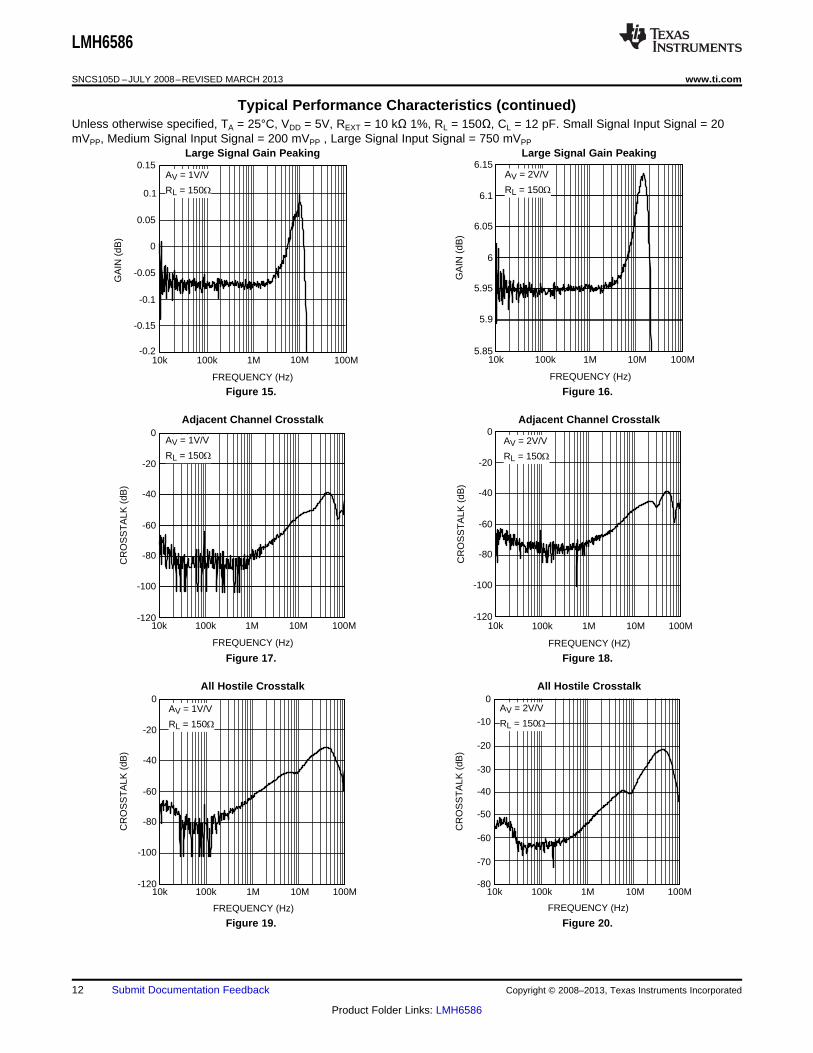
Typical Performance Characteristics (continued)Unless otherwise specified, TA = 25°C, VDD = 5V, REXT = 10 kΩ 1%, RL = 150Ω, CL = 12 pF. Small Signal Input Signal = 20mVPP, Medium Signal Input Signal = 200 mVPP , Large Signal Input Signal = 750 mVPP
Large Signal Gain Peaking Large Signal Gain Peaking
Figure 15. Figure 16.
Adjacent Channel Crosstalk Adjacent Channel Crosstalk
Figure 17. Figure 18.
All Hostile Crosstalk All Hostile Crosstalk
Figure 19. Figure 20.
12 Submit Documentation Feedback Copyright © 2008–2013, Texas Instruments Incorporated
Product Folder Links: LMH6586

INPUT10 mV/DIV
25 ns/DIV
OUTPUT20 mV/DIV
AV = 2V/V
RL = 150:INPUT
10 mV/DIV
25 ns/DIV
OUTPUT10 mV/DIV
AV = 1V/V
CL = 30 pF
INPUT10 mV/DIV
25 ns/DIV
OUTPUT20 mV/DIV
AV = 2V/V
RL = 1 k:
INPUT10 mV/DIV
25 ns/DIV
OUTPUT10 mV/DIV
AV = 1V/V
RL = 150:
10 100 1M 10M 100M-110
-100
-90
-80
-70
-60
-50
-40
-30
-20
OF
F IS
OLA
TIO
N (
dB)
FREQUENCY (Hz)
AV = 2V/V
RL = 150:INPUT
10 mV/DIV
25 ns/DIV
OUTPUT10 mV/DIV
AV = 1V/V
RL = 1 k:
LMH6586
www.ti.com SNCS105D –JULY 2008–REVISED MARCH 2013
Typical Performance Characteristics (continued)Unless otherwise specified, TA = 25°C, VDD = 5V, REXT = 10 kΩ 1%, RL = 150Ω, CL = 12 pF. Small Signal Input Signal = 20mVPP, Medium Signal Input Signal = 200 mVPP , Large Signal Input Signal = 750 mVPP
Off Isolation Small Signal Pulse Response
Figure 21. Figure 22.
Small Signal Pulse Response Small Signal Pulse Response
Figure 23. Figure 24.
Small Signal Pulse Response Small Signal Pulse Response with Capacitive Load
Figure 25. Figure 26.
Copyright © 2008–2013, Texas Instruments Incorporated Submit Documentation Feedback 13
Product Folder Links: LMH6586
INPUT50 mV/DIV
25 ns/DIV
OUTPUT100 mV/DIV
AV = 2V/V
RL = 150:
INPUT50 mV/DIV
25 ns/DIV
OUTPUT50 mV/DIV
AV = 1V/V
CL = 30 pF
INPUT50 mV/DIV
25 ns/DIV
OUTPUT100 mV/DIV
AV = 2V/V
RL = 1 k:
INPUT50 mV/DIV
25 ns/DIV
OUTPUT50 mV/DIV
AV = 1V/V
RL = 150:
INPUT10 mV/DIV
25 ns/DIV
OUTPUT10 mV/DIV
AV = 2V/V
CL = 30 pF
INPUT50 mV/DIV
25 ns/DIV
OUTPUT50 mV/DIV
AV = 1V/V
RL = 1 k:
LMH6586
SNCS105D –JULY 2008–REVISED MARCH 2013 www.ti.com
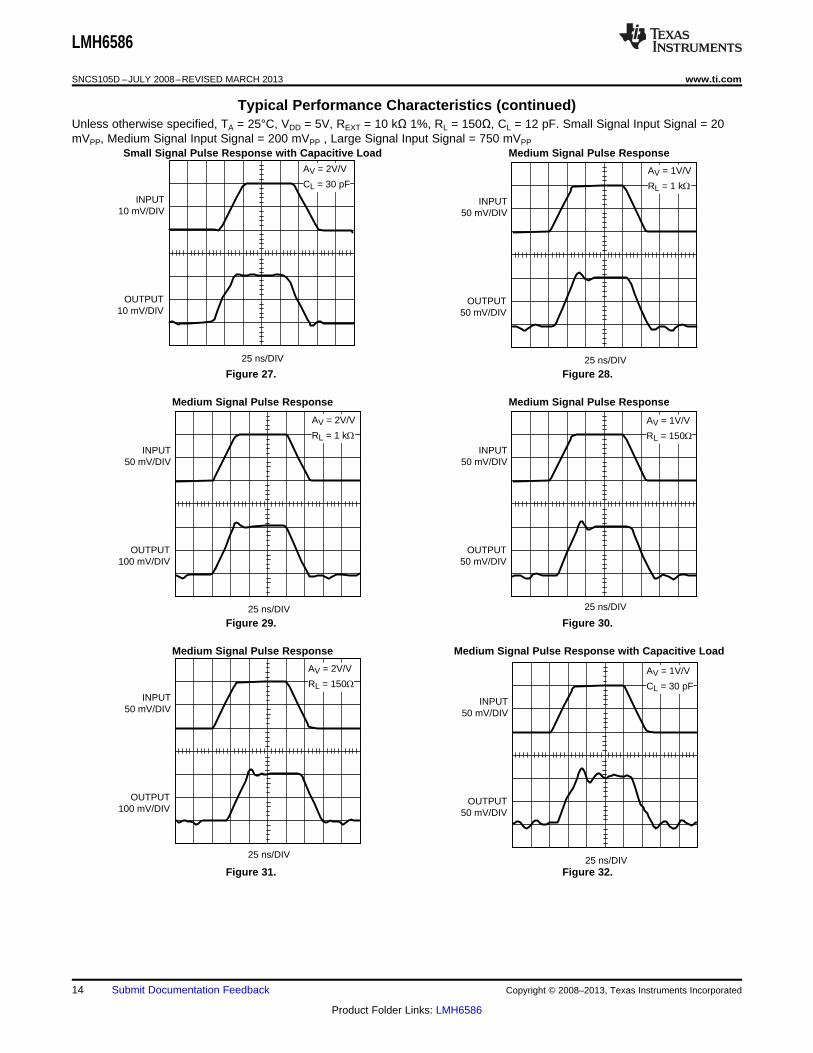
Typical Performance Characteristics (continued)Unless otherwise specified, TA = 25°C, VDD = 5V, REXT = 10 kΩ 1%, RL = 150Ω, CL = 12 pF. Small Signal Input Signal = 20mVPP, Medium Signal Input Signal = 200 mVPP , Large Signal Input Signal = 750 mVPP
Small Signal Pulse Response with Capacitive Load Medium Signal Pulse Response
Figure 27. Figure 28.
Medium Signal Pulse Response Medium Signal Pulse Response
Figure 29. Figure 30.
Medium Signal Pulse Response Medium Signal Pulse Response with Capacitive Load
Figure 31. Figure 32.
14 Submit Documentation Feedback Copyright © 2008–2013, Texas Instruments Incorporated
Product Folder Links: LMH6586
INPUT200 mV/DIV
25 ns/DIV
OUTPUT500 mV/DIV
AV = 2V/V
RL = 150:
INPUT200 mV/DIV
25 ns/DIV
OUTPUT200 mV/DIV
AV = 1V/V
CL = 30 pF
INPUT200 mV/DIV
25 ns/DIV
OUTPUT500 mV/DIV
AV = 2V/V
RL = 1 k:
INPUT200 mV/DIV
25 ns/DIV
OUTPUT200 mV/DIV
AV = 1V/V
RL = 150:
INPUT50 mV/DIV
25 ns/DIV
OUTPUT100 mV/DIV
AV = 2V/V
CL = 30 pFINPUT
200 mV/DIV
25 ns/DIV
OUTPUT200 mV/DIV
AV = 1V/V
RL = 1 k:
LMH6586
www.ti.com SNCS105D –JULY 2008–REVISED MARCH 2013
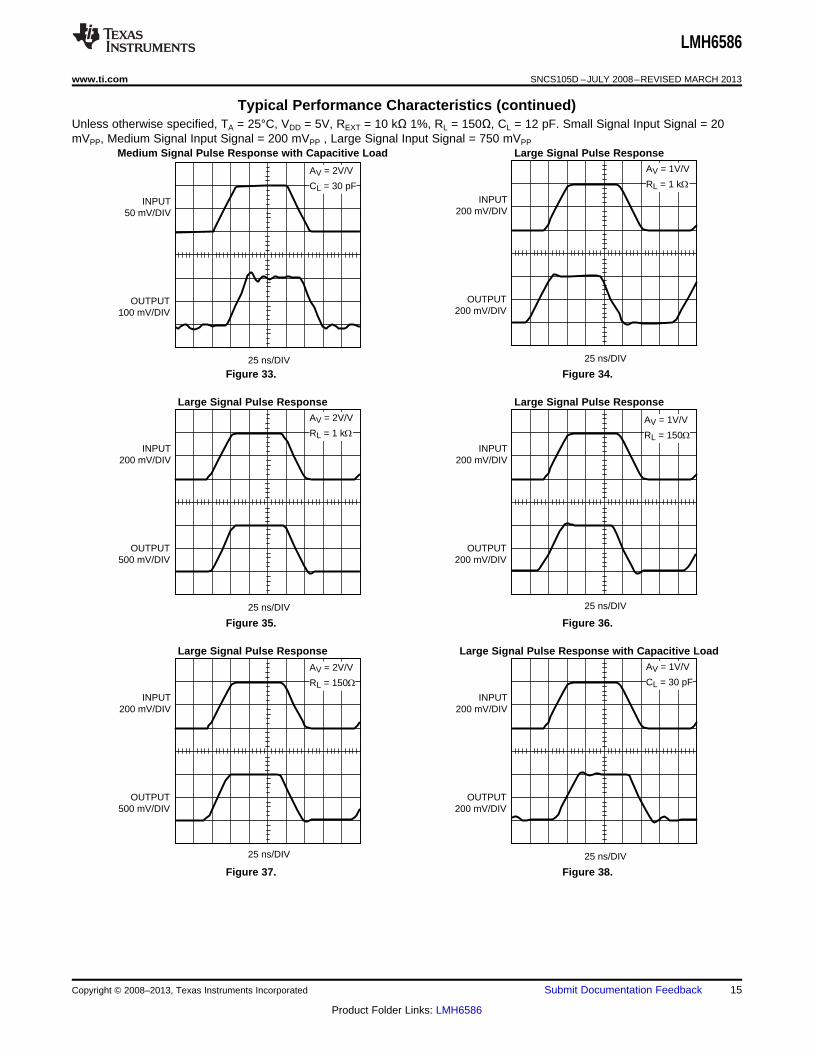
Typical Performance Characteristics (continued)Unless otherwise specified, TA = 25°C, VDD = 5V, REXT = 10 kΩ 1%, RL = 150Ω, CL = 12 pF. Small Signal Input Signal = 20mVPP, Medium Signal Input Signal = 200 mVPP , Large Signal Input Signal = 750 mVPP
Medium Signal Pulse Response with Capacitive Load Large Signal Pulse Response
Figure 33. Figure 34.
Large Signal Pulse Response Large Signal Pulse Response
Figure 35. Figure 36.
Large Signal Pulse Response Large Signal Pulse Response with Capacitive Load
Figure 37. Figure 38.
Copyright © 2008–2013, Texas Instruments Incorporated Submit Documentation Feedback 15
Product Folder Links: LMH6586
0.6 0.7 0.8 0.9 1 1.1 1.2 1.3
OUTPUT VIDEO LEVEL (V)
DIF
FE
RE
NT
IAL
GA
IN0.
01%
/DIV
AV = 1V/V
RL = 1 k:REF
0.6 0.7 0.8 0.9 1 1.1 1.2
OUTPUT VIDEO LEVEL (V)
DIF
FE
RE
NT
IAL
PH
AS
E0.
02°/D
IV
1.3
AV = 2V/V
RL = 150:
REF
0.6 0.7 0.8 0.9 1 1.1 1.2 1.3
DIF
FE
RE
NT
IAL
PH
AS
E0.
01°/D
IV
OUTPUT VIDEO LEVEL (V)
AV = 1V/V
RL = 150:
REF
REF
0.6 0.7 0.8 0.9 1 1.1 1.2 1.3
DIF
FE
RE
NT
IAL
PH
AS
E0.
01°/D
IV
OUTPUT VIDEO LEVEL (V)
AV = 2V/V
RL = 1 k:
0.6 0.7 0.8 0.9 1 1.1 1.2 1.3
OUTPUT VIDEO LEVEL (V)
DIF
FE
RE
NT
IAL
PH
AS
E0.
02°/D
IV
AV = 1V/V
RL = 1 k:
REFINPUT200 mV/DIV
25 ns/DIV
OUTPUT500 mV/DIV
AV = 2V/V
CL = 30 pF
LMH6586
SNCS105D –JULY 2008–REVISED MARCH 2013 www.ti.com
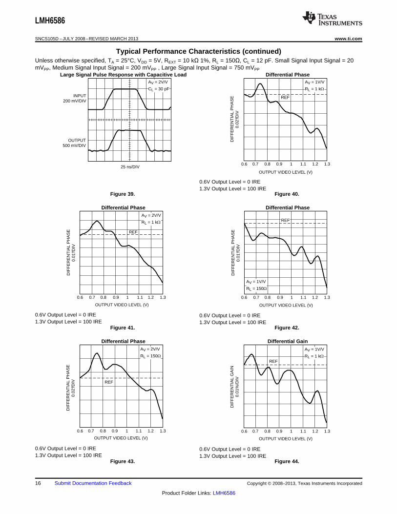
Typical Performance Characteristics (continued)Unless otherwise specified, TA = 25°C, VDD = 5V, REXT = 10 kΩ 1%, RL = 150Ω, CL = 12 pF. Small Signal Input Signal = 20mVPP, Medium Signal Input Signal = 200 mVPP , Large Signal Input Signal = 750 mVPP
Large Signal Pulse Response with Capacitive Load Differential Phase
0.6V Output Level = 0 IRE1.3V Output Level = 100 IRE
Figure 39. Figure 40.
Differential Phase Differential Phase
0.6V Output Level = 0 IRE 0.6V Output Level = 0 IRE1.3V Output Level = 100 IRE 1.3V Output Level = 100 IRE
Figure 41. Figure 42.
Differential Phase Differential Gain
0.6V Output Level = 0 IRE 0.6V Output Level = 0 IRE1.3V Output Level = 100 IRE 1.3V Output Level = 100 IRE
Figure 43. Figure 44.
16 Submit Documentation Feedback Copyright © 2008–2013, Texas Instruments Incorporated
Product Folder Links: LMH6586
1M 10M
FREQUENCY (Hz)
-100
-90
-80
-70
-60
-50
-40
HA
RM
ON
IC D
IST
OR
TIO
N (
dB)
AV = 2V/V
RL = 150:
1M 10M
FREQUENCY (Hz)
-100
-90
-80
-70
-60
-50
-40
HA
RM
ON
IC D
IST
OR
TIO
N (
dB)
AV = 1V/V
RL = 150:
0.6 0.7 0.8 0.9 1 1.1 1.2 1.3
OUTPUT VIDEO LEVEL (V)
DIF
FE
RE
NT
IAL
GA
IN0.
01%
/DIV
AV = 2V/V
RL = 150:
REF
0.6 0.7 0.8 0.9 1 1.1 1.2 1.3
DIF
FE
RE
NT
IAL
GA
IN0.
01%
/DIV
OUTPUT VIDEO LEVEL (V)
AV = 2V/V
RL = 1 k:
REF
0.6 0.7 0.8 0.9 1 1.1 1.2 1.3
DIF
FE
RE
NT
IAL
GA
IN0.
02%
/DIV
OUTPUT VIDEO LEVEL (V)
AV = 1V/V
RL = 150:
REF
LMH6586
www.ti.com SNCS105D –JULY 2008–REVISED MARCH 2013
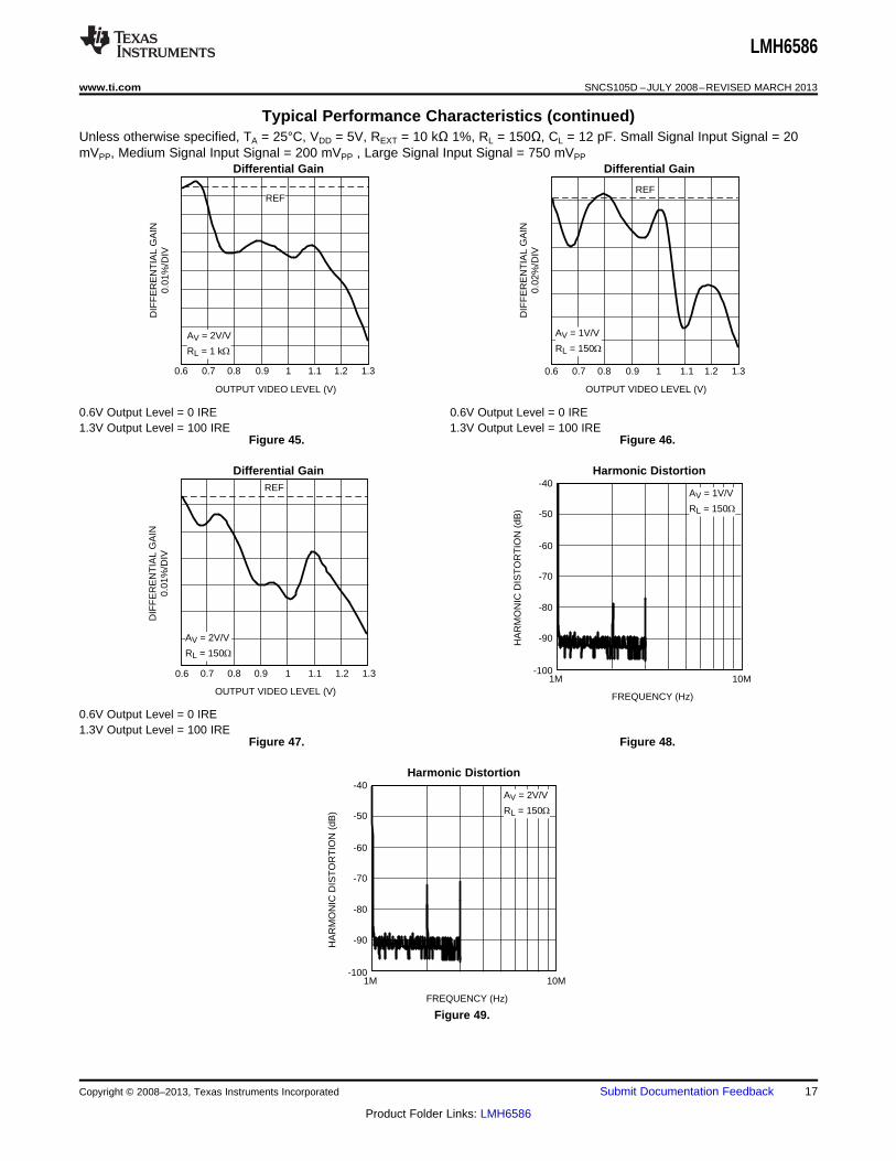
Typical Performance Characteristics (continued)Unless otherwise specified, TA = 25°C, VDD = 5V, REXT = 10 kΩ 1%, RL = 150Ω, CL = 12 pF. Small Signal Input Signal = 20mVPP, Medium Signal Input Signal = 200 mVPP , Large Signal Input Signal = 750 mVPP
Differential Gain Differential Gain
0.6V Output Level = 0 IRE 0.6V Output Level = 0 IRE1.3V Output Level = 100 IRE 1.3V Output Level = 100 IRE
Figure 45. Figure 46.
Differential Gain Harmonic Distortion
0.6V Output Level = 0 IRE1.3V Output Level = 100 IRE
Figure 47. Figure 48.
Harmonic Distortion
Figure 49.
Copyright © 2008–2013, Texas Instruments Incorporated Submit Documentation Feedback 17
Product Folder Links: LMH6586
LMH6586
SNCS105D –JULY 2008–REVISED MARCH 2013 www.ti.com
APPLICATION INFORMATION
FUNCTIONAL OVERVIEW
The LMH6586 is a non-blocking, analog video crosspoint switch with 32 input channels and 16 output channels.The inputs have integrated DC restore clamp circuits for biasing the AC-coupled video inputs. The fully bufferedoutputs have selectable gain and can drive one back-terminated video load (150Ω). The LMH6586 includes anextra output (VOUT_16) with 1X fixed gain that can be used to feed any input's video signal to an external videosync separator, such as the LMH1980 or LMH1981.
Each input and each output can be individually placed in shutdown mode by programming the input shutdownand output shutdown registers, respectively. Additionally, the PWDN pin (pin 70) can be set high to enable PowerDown mode, which shuts down all input and output video channels while preserving all register settings.
The LMH6586 also features both video detection and sync detection functions on each input channel. Additionalflexibility is provided by user-defined threshold levels for both video and sync detection features. The status ofboth detection schemes can be read from the video and sync detection status registers. Additionally, the FLAGoutput (pin 75) can be used to indicate if video detection or sync detection is triggered on any combination ofinput channels and detection types enabled by the user.
OUTPUT BUFFER GAIN
The LMH6586 has an output buffer with a selectable gain of 1X or 2X. When the GAIN_SEL input (pin 61) is setlow, output channels 0–15 will have a gain of 1X. When it is set high, they will have a gain of 2X. Regardless ofthe gain select setting, output channel 16 has 1X fixed gain since the output is intended to drive an optionalexternal sync separator through a 0.1 µF capacitor and no load termination.
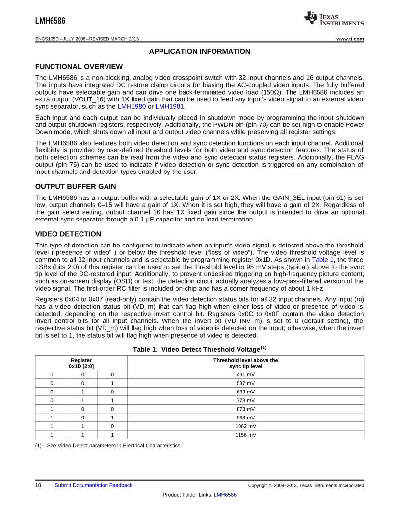
VIDEO DETECTION
This type of detection can be configured to indicate when an input's video signal is detected above the thresholdlevel (“presence of video” ) or below the threshold level (“loss of video”). The video threshold voltage level iscommon to all 32 input channels and is selectable by programming register 0x1D. As shown in Table 1, the threeLSBs (bits 2:0) of this register can be used to set the threshold level in 95 mV steps (typical) above to the synctip level of the DC-restored input. Additionally, to prevent undesired triggering on high-frequency picture content,such as on-screen display (OSD) or text, the detection circuit actually analyzes a low-pass-filtered version of thevideo signal. The first-order RC filter is included on-chip and has a corner frequency of about 1 kHz.
Registers 0x04 to 0x07 (read-only) contain the video detection status bits for all 32 input channels. Any input (m)has a video detection status bit (VD_m) that can flag high when either loss of video or presence of video isdetected, depending on the respective invert control bit. Registers 0x0C to 0x0F contain the video detectioninvert control bits for all input channels. When the invert bit (VD_INV_m) is set to 0 (default setting), therespective status bit (VD_m) will flag high when loss of video is detected on the input; otherwise, when the invertbit is set to 1, the status bit will flag high when presence of video is detected.
Table 1. Video Detect Threshold Voltage (1)
Register Threshold level above the0x1D [2:0] sync tip level
0 0 0 491 mV
0 0 1 587 mV
0 1 0 683 mV
0 1 1 778 mV
1 0 0 873 mV
1 0 1 968 mV
1 1 0 1062 mV
1 1 1 1156 mV
(1) See Video Detect parameters in Electrical Characteristics
18 Submit Documentation Feedback Copyright © 2008–2013, Texas Instruments Incorporated
Product Folder Links: LMH6586
LMH6586
www.ti.com SNCS105D –JULY 2008–REVISED MARCH 2013
The following example illustrates a practical use of video detection in a real-world system. A bank's ATMsurveillance system could consist of a video camera, a LMH6586 crosspoint switch, a video recorder, and controlsystem. When no one is using the ATM, the area being monitored by the camera could have strong backlighting,so the camera would output a normally high video level. When a person approaches the area, most of thebacklighting would be blocked by the person and cause a measurable decrease in the video level. This changein camera's video level could be detected by the LMH6586, which could then flag the security system to beginrecording of the activity. Once the person leaves the area, the LMH6586 could clear the flag.
SYNC DETECTION
The LMH6586 also features a sync detection circuit that can indicate when an input's negative-going sync pulseis not detected below the threshold level (“loss of sync”). The sync threshold voltage level is common to all 32input channels and is defined by the bias voltage on the VREF_SYNC input (pin 65), which may be set using asimple voltage divider circuit. The recommended voltage level at the VREF_SYNC pin is 350 mV to ensureproper operation.
Registers 0x00 to 0x03 (read-only) contain the sync detection status bits for all 32 input channels. Any input (m)has a sync detection status bit (SD_m) that can flag high when a loss of sync is detected; otherwise, the statusbit will be low to indicate presence of sync.
DETECTION FLAG OUTPUT
The FLAG output (pin 75) can flag high if either video detection or sync detection is triggered based on the user-defined enable settings for the video and sync detection status bits. Any of the input's video detection status bits(VD_m) and sync detection status bits (SD_m) can be logically OR-ed into this single FLAG output pin. Registers0x10 to 0x13 contain the video detection enable bits and registers 0x14 to 0x17 contain the sync detectionenable bits for all input channels. Any input (m) has both a video detection enable bit (VD_EN_m) and a syncdetection enable bit (SD_EN_m). When any enable bit is set low, the respective status bit will be excluded fromthe OR-ing function used to set the FLAG output; otherwise, when the enable bit is set high, the respective statusbit will be included in the FLAG output function. Therefore, the FLAG will only logical-OR the status bits of thechannel(s) and type(s) of detection that are specifically enabled by the user.
SWITCH MATRIX
The LMH6586 uses 512 CMOS analog switches to form a 32 x 16 crosspoint switch. The LMH6586 is a non-blocking crosspoint switch which means that any one of the 32 inputs can be routed to any of the 16 outputs.The switch can only be configured by programming through the I2C bus interface.
DC RESTORATION
Because the LMH6586 uses a single 5V supply and typical composite video signals contain signal componentsboth above and below 0V (video blanking level), proper input signal biasing is required to ensure the video signalis within the operating range of the amplifier. To simplify the external biasing circuitry, each input of the LMH6586has a dedicated DC restore clamp circuit to allow AC-coupled input operation using a 0.1 uF coupling capacitor.Please refer to AC COUPLING for details on how the coupling capacitor value was determined.
AC COUPLING
Each video input uses an integrated DC restore clamp circuit to servo the sync tip of the AC-coupled video inputsignal to the DC voltage received at the VREF_CLAMP input (pin 66). For proper AC-coupled operation, theLMH6586 requires video signals with negative sync pulses. The VREF_CLAMP level can be set in range of 300mV to 1.0V using a voltage divider network. For optimum performance and reduced power consumption, it isrecommended to set VREF_CLAMP to 300 mV. Therefore, assuming a video input amplitude of 1VPP, the bottomof the sync tip level would be clamped to 300 mV above ground and the peak white video level would be at 1.3V.
Copyright © 2008–2013, Texas Instruments Incorporated Submit Documentation Feedback 19
Product Folder Links: LMH6586
-
+300 mV
C75:
7.8 mA
1.37 PA
+5V
CLAMP CIRCUIT
V_CLAMP
VIN
LMH6586
SNCS105D –JULY 2008–REVISED MARCH 2013 www.ti.com
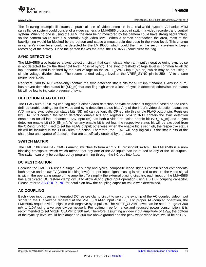
Figure 50. Input Video Signal Before DC Restore Clamp
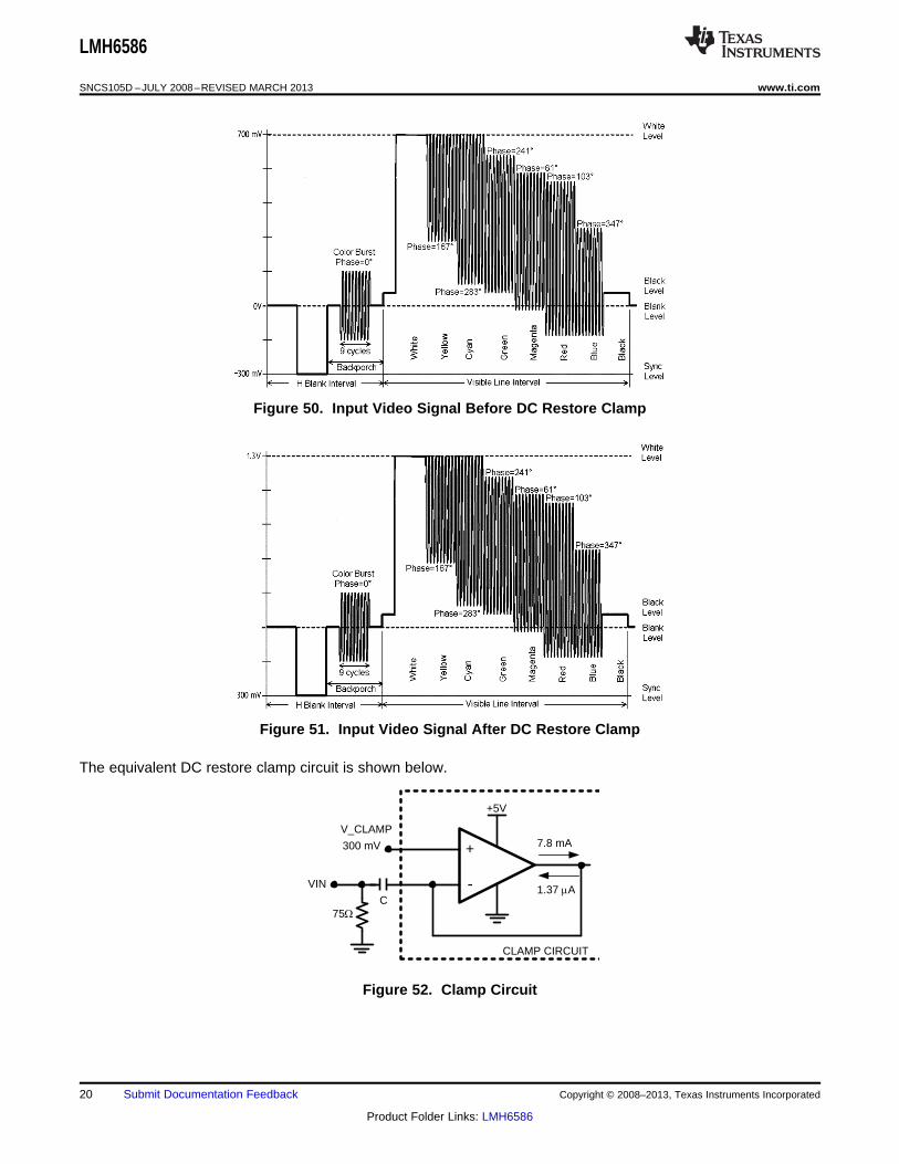
Figure 51. Input Video Signal After DC Restore Clamp
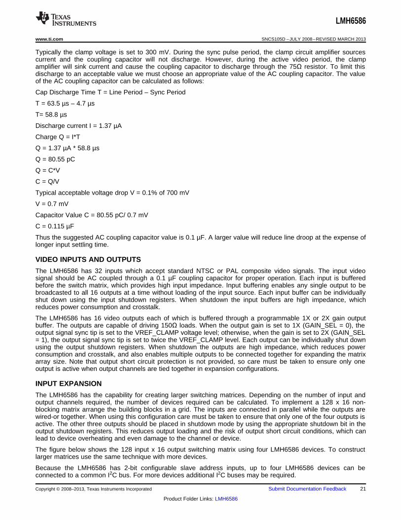
The equivalent DC restore clamp circuit is shown below.
Figure 52. Clamp Circuit
20 Submit Documentation Feedback Copyright © 2008–2013, Texas Instruments Incorporated
Product Folder Links: LMH6586
LMH6586
www.ti.com SNCS105D –JULY 2008–REVISED MARCH 2013
Typically the clamp voltage is set to 300 mV. During the sync pulse period, the clamp circuit amplifier sourcescurrent and the coupling capacitor will not discharge. However, during the active video period, the clampamplifier will sink current and cause the coupling capacitor to discharge through the 75Ω resistor. To limit thisdischarge to an acceptable value we must choose an appropriate value of the AC coupling capacitor. The valueof the AC coupling capacitor can be calculated as follows:
Cap Discharge Time T = Line Period – Sync Period
T = 63.5 µs – 4.7 µs
T= 58.8 µs
Discharge current I = 1.37 µA
Charge Q = I*T
Q = 1.37 µA * 58.8 µs
Q = 80.55 pC
Q = C*V
C = Q/V
Typical acceptable voltage drop V = 0.1% of 700 mV
V = 0.7 mV
Capacitor Value C = 80.55 pC/ 0.7 mV
C = 0.115 µF
Thus the suggested AC coupling capacitor value is 0.1 µF. A larger value will reduce line droop at the expense oflonger input settling time.
VIDEO INPUTS AND OUTPUTS
The LMH6586 has 32 inputs which accept standard NTSC or PAL composite video signals. The input videosignal should be AC coupled through a 0.1 µF coupling capacitor for proper operation. Each input is bufferedbefore the switch matrix, which provides high input impedance. Input buffering enables any single output to bebroadcasted to all 16 outputs at a time without loading of the input source. Each input buffer can be individuallyshut down using the input shutdown registers. When shutdown the input buffers are high impedance, whichreduces power consumption and crosstalk.
The LMH6586 has 16 video outputs each of which is buffered through a programmable 1X or 2X gain outputbuffer. The outputs are capable of driving 150Ω loads. When the output gain is set to 1X (GAIN_SEL = 0), theoutput signal sync tip is set to the VREF_CLAMP voltage level; otherwise, when the gain is set to 2X (GAIN_SEL= 1), the output signal sync tip is set to twice the VREF_CLAMP level. Each output can be individually shut downusing the output shutdown registers. When shutdown the outputs are high impedance, which reduces powerconsumption and crosstalk, and also enables multiple outputs to be connected together for expanding the matrixarray size. Note that output short circuit protection is not provided, so care must be taken to ensure only oneoutput is active when output channels are tied together in expansion configurations.
INPUT EXPANSION
The LMH6586 has the capability for creating larger switching matrices. Depending on the number of input andoutput channels required, the number of devices required can be calculated. To implement a 128 x 16 non-blocking matrix arrange the building blocks in a grid. The inputs are connected in parallel while the outputs arewired-or together. When using this configuration care must be taken to ensure that only one of the four outputs isactive. The other three outputs should be placed in shutdown mode by using the appropriate shutdown bit in theoutput shutdown registers. This reduces output loading and the risk of output short circuit conditions, which canlead to device overheating and even damage to the channel or device.
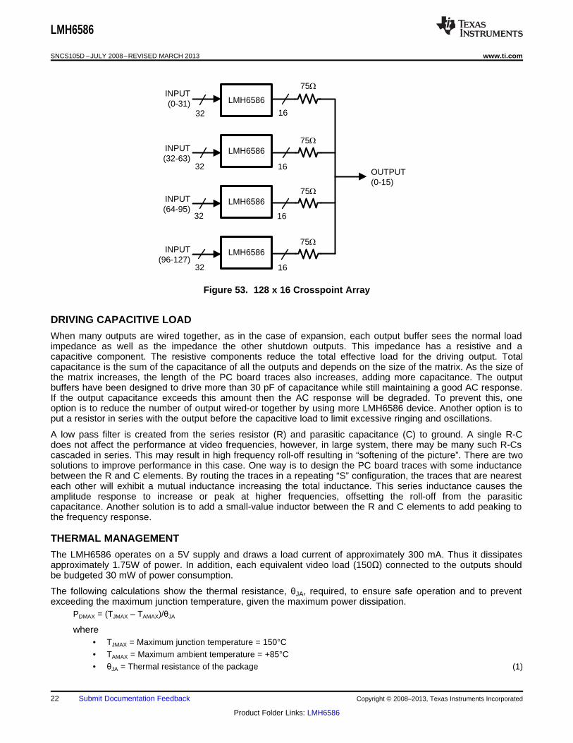
The figure below shows the 128 input x 16 output switching matrix using four LMH6586 devices. To constructlarger matrices use the same technique with more devices.
Because the LMH6586 has 2-bit configurable slave address inputs, up to four LMH6586 devices can beconnected to a common I2C bus. For more devices additional I2C buses may be required.
Copyright © 2008–2013, Texas Instruments Incorporated Submit Documentation Feedback 21
Product Folder Links: LMH6586
LMH6586
LMH6586
LMH6586
LMH6586
OUTPUT(0-15)
INPUT(0-31)
INPUT(32-63)
INPUT(64-95)
INPUT(96-127)
75:
75:
75:
75:
16
16
16
16
32
32
32
32
LMH6586
SNCS105D –JULY 2008–REVISED MARCH 2013 www.ti.com
Figure 53. 128 x 16 Crosspoint Array
DRIVING CAPACITIVE LOAD
When many outputs are wired together, as in the case of expansion, each output buffer sees the normal loadimpedance as well as the impedance the other shutdown outputs. This impedance has a resistive and acapacitive component. The resistive components reduce the total effective load for the driving output. Totalcapacitance is the sum of the capacitance of all the outputs and depends on the size of the matrix. As the size ofthe matrix increases, the length of the PC board traces also increases, adding more capacitance. The outputbuffers have been designed to drive more than 30 pF of capacitance while still maintaining a good AC response.If the output capacitance exceeds this amount then the AC response will be degraded. To prevent this, oneoption is to reduce the number of output wired-or together by using more LMH6586 device. Another option is toput a resistor in series with the output before the capacitive load to limit excessive ringing and oscillations.
A low pass filter is created from the series resistor (R) and parasitic capacitance (C) to ground. A single R-Cdoes not affect the performance at video frequencies, however, in large system, there may be many such R-Cscascaded in series. This may result in high frequency roll-off resulting in “softening of the picture”. There are twosolutions to improve performance in this case. One way is to design the PC board traces with some inductancebetween the R and C elements. By routing the traces in a repeating “S” configuration, the traces that are nearesteach other will exhibit a mutual inductance increasing the total inductance. This series inductance causes theamplitude response to increase or peak at higher frequencies, offsetting the roll-off from the parasiticcapacitance. Another solution is to add a small-value inductor between the R and C elements to add peaking tothe frequency response.
THERMAL MANAGEMENT
The LMH6586 operates on a 5V supply and draws a load current of approximately 300 mA. Thus it dissipatesapproximately 1.75W of power. In addition, each equivalent video load (150Ω) connected to the outputs shouldbe budgeted 30 mW of power consumption.
The following calculations show the thermal resistance, θJA, required, to ensure safe operation and to preventexceeding the maximum junction temperature, given the maximum power dissipation.
PDMAX = (TJMAX – TAMAX)/θJA
where• TJMAX = Maximum junction temperature = 150°C• TAMAX = Maximum ambient temperature = +85°C• θJA = Thermal resistance of the package (1)
22 Submit Documentation Feedback Copyright © 2008–2013, Texas Instruments Incorporated
Product Folder Links: LMH6586
PDMAX = VS x ISMAX + 6 (VS ± VOUTi) x VOUTi
RLi
n
i = 1
LMH6586
www.ti.com SNCS105D –JULY 2008–REVISED MARCH 2013
The maximum power dissipation actually produced by an IC is the total quiescent supply current times the totalpower supply voltage, plus the power in the IC due to the load, or:
where• VS = Supply voltage = 5V• ISMAX = Maximum quiescent supply current = 300 mA• VOUT = Maximum output voltage of the application = 2.6V• RL = Load resistance tied to ground = 150Ω• n = 1 to 16 channels (2)
Calculating:
PDMAX = 2.2656
The required θJA to dissipate PDMAX is = (TJMAX – TAMAX)/PDMAX
The table below shows the θJA values with airflow and different heatsinks.
LMH6586VS 80-Pin TQFT 0 LFPM 0 LFPM 0 LFPM 0 LFPM @2.8 225 LFPM @ 500 LFPM @LMHXPT @ 0.50 watt @ 1.0 watt @ 2.0 watt watt 2.8 watt 2.8 watt
Analog Video Crosspoint Board
NO Heat Sink 32.2 30.9 29.4 28.6 26.8 25.3
Small Tower 25.5 24.6 23.6 22.9 19.2 15.9x y = 9.57x9.69 mm/ht. 6.28 mm
Aluminum 12 rail 25.2 24.1 23.0 22.2 16.4 14.2x y = 9.82x10.73 mm/ht.10.07 mm
Anodized 9 rail 24.4 23.3 22.1 21.3 15.6 13.6x y = 6.10x7.30 mm/ht. 13.67 mm
Round Tower 24.2 23.9 22.9 22.4 18.2 15.4diameter = 14.35 mm/ht. 4.47 mm
REXT RESISTOR
The REXT external resistor (pin 67) establishes the internal bias current and precise reference voltage for theLMH6586. For optimal performance, REXT should be a 10 kΩ 1% precision resistor with a low temperaturecoefficient to ensure proper operation over a wide temperature range. Using a REXT resistor with less precisionmay result in reduced performance against temperature, supply voltage, input signal, or part-to-part variations.
SYNC SEPARATOR OUTPUT
In addition to the 16 video outputs, the LMH6586 has an extra output (V_OUT16) which can select any inputchannel. This channel's output buffer only has a gain of 1 since it is not meant to drive a 150Ω video load.Instead, this video output can be AC coupled to a non-terminated input of an external video sync separator, suchas TI's LMH1980 or LMH1981. The sync separator can extract the synchronization (sync) timing signals, whichcan be useful for video triggering or phase-locked loop (PLL) clock generation circuits. Refer to the LMH1980 orLMH1981 datasheet for more information about these sync separator devices.
I2C INTERFACE
A microcontroller can be used to configure the LMH6586 via the I2C interface. The protocol of the interfacebegins with a start pulse followed by a byte comprised of a seven-bit slave device address and a read/write bit asthe LSB. The two lowest bits of the seven-bit slave address are defined by the external connections of inputsADDR[1] (pin 72) and ADDR[0] (pin 71), where ADDR[0] is the least significant bit. Because there are fourdifferent combinations of the two ADDR pins, it's possible to have up to four different LMH6586 devices withunique slave addresses on a common I2C bus. See I2C Device Slave Address Lookup Table.
Copyright © 2008–2013, Texas Instruments Incorporated Submit Documentation Feedback 23
Product Folder Links: LMH6586
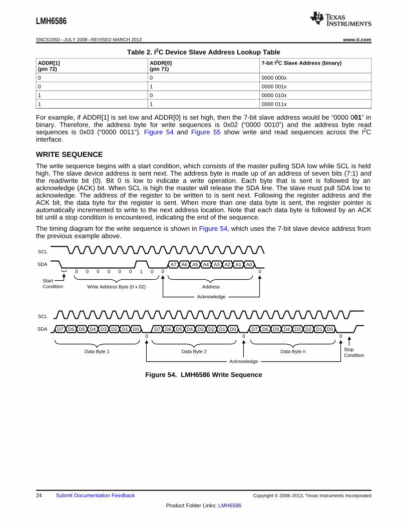
SCL
SDA A7 A6 A5 A4 A3 A2 A1 A0
0 01000000 0
Address
SCL
SDA D7 D6 D5 D4 D3 D2 D1 D0D7 D6 D5 D4 D3 D2 D1 D0
0 0
Data Byte 2 Data Byte n
D7 D6 D5 D4 D3 D2 D1 D0
0
Data Byte 1
Write Address Byte (0 x 02)
Acknowledge
Acknowledge
StopCondition
StartCondition
LMH6586
SNCS105D –JULY 2008–REVISED MARCH 2013 www.ti.com
Table 2. I2C Device Slave Address Lookup Table
ADDR[1] ADDR[0] 7-bit I2C Slave Address (binary)(pin 72) (pin 71)
0 0 0000 000x
0 1 0000 001x
1 0 0000 010x
1 1 0000 011x
For example, if ADDR[1] is set low and ADDR[0] is set high, then the 7-bit slave address would be “0000 001” inbinary. Therefore, the address byte for write sequences is 0x02 (“0000 0010”) and the address byte readsequences is 0x03 (“0000 0011”). Figure 54 and Figure 55 show write and read sequences across the I2Cinterface.
WRITE SEQUENCE
The write sequence begins with a start condition, which consists of the master pulling SDA low while SCL is heldhigh. The slave device address is sent next. The address byte is made up of an address of seven bits (7:1) andthe read/write bit (0). Bit 0 is low to indicate a write operation. Each byte that is sent is followed by anacknowledge (ACK) bit. When SCL is high the master will release the SDA line. The slave must pull SDA low toacknowledge. The address of the register to be written to is sent next. Following the register address and theACK bit, the data byte for the register is sent. When more than one data byte is sent, the register pointer isautomatically incremented to write to the next address location. Note that each data byte is followed by an ACKbit until a stop condition is encountered, indicating the end of the sequence.
The timing diagram for the write sequence is shown in Figure 54, which uses the 7-bit slave device address fromthe previous example above.
Figure 54. LMH6586 Write Sequence
24 Submit Documentation Feedback Copyright © 2008–2013, Texas Instruments Incorporated
Product Folder Links: LMH6586
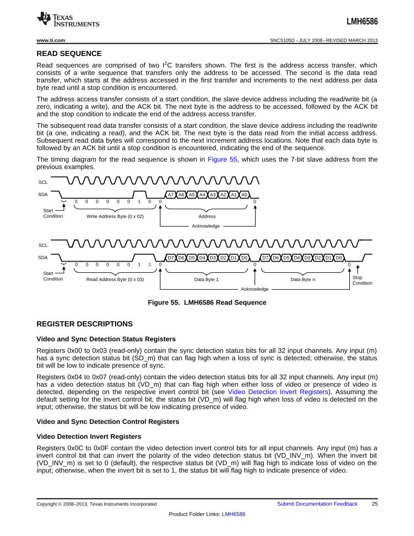
SCL
SDA A7 A6 A5 A4 A3 A2 A1 A0
0 01000000 0
Address
SCL
SDA D7 D6 D5 D4 D3 D2 D1 D0D6 D5 D4 D3 D2 D1 D0
0 0
Data Byte 1 Data Byte n
0
Write Address Byte (0 x 02)
Acknowledge
Acknowledge
StopCondition
StartCondition
D7
11000000
StartCondition Read Address Byte (0 x 03)
LMH6586
www.ti.com SNCS105D –JULY 2008–REVISED MARCH 2013
READ SEQUENCE
Read sequences are comprised of two I2C transfers shown. The first is the address access transfer, whichconsists of a write sequence that transfers only the address to be accessed. The second is the data readtransfer, which starts at the address accessed in the first transfer and increments to the next address per databyte read until a stop condition is encountered.
The address access transfer consists of a start condition, the slave device address including the read/write bit (azero, indicating a write), and the ACK bit. The next byte is the address to be accessed, followed by the ACK bitand the stop condition to indicate the end of the address access transfer.
The subsequent read data transfer consists of a start condition, the slave device address including the read/writebit (a one, indicating a read), and the ACK bit. The next byte is the data read from the initial access address.Subsequent read data bytes will correspond to the next increment address locations. Note that each data byte isfollowed by an ACK bit until a stop condition is encountered, indicating the end of the sequence.
The timing diagram for the read sequence is shown in Figure 55, which uses the 7-bit slave address from theprevious examples.
Figure 55. LMH6586 Read Sequence
REGISTER DESCRIPTIONS
Video and Sync Detection Status Registers
Registers 0x00 to 0x03 (read-only) contain the sync detection status bits for all 32 input channels. Any input (m)has a sync detection status bit (SD_m) that can flag high when a loss of sync is detected; otherwise, the statusbit will be low to indicate presence of sync.
Registers 0x04 to 0x07 (read-only) contain the video detection status bits for all 32 input channels. Any input (m)has a video detection status bit (VD_m) that can flag high when either loss of video or presence of video isdetected, depending on the respective invert control bit (see Video Detection Invert Registers). Assuming thedefault setting for the invert control bit, the status bit (VD_m) will flag high when loss of video is detected on theinput; otherwise, the status bit will be low indicating presence of video.
Video and Sync Detection Control Registers
Video Detection Invert Registers
Registers 0x0C to 0x0F contain the video detection invert control bits for all input channels. Any input (m) has ainvert control bit that can invert the polarity of the video detection status bit (VD_INV_m). When the invert bit(VD_INV_m) is set to 0 (default), the respective status bit (VD_m) will flag high to indicate loss of video on theinput; otherwise, when the invert bit is set to 1, the status bit will flag high to indicate presence of video.
Copyright © 2008–2013, Texas Instruments Incorporated Submit Documentation Feedback 25
Product Folder Links: LMH6586
LMH6586
SNCS105D –JULY 2008–REVISED MARCH 2013 www.ti.com
Video and Sync Detection Enable Registers:
Registers 0x10 to 0x13 contain the video detection enable bits and registers 0x14 to 0x17 contain the syncdetection enable bits for all input channels. Any input (m) has both a video detection enable bit (VD_EN_m) anda sync detection enable bit (SD_EN_m). When any enable bit is set low, the respective status bit will be excludedfrom the OR-ing function used to set the FLAG output; otherwise, when the enable bit is set high, the respectivestatus bit will be included in the FLAG output function. Therefore, the FLAG will only logical-OR the status bits ofthe channel(s) and type(s) of detection that are specifically enabled by the user as described in DETECTIONFLAG OUTPUT.
Video Detection Threshold Control Register
The video threshold voltage level is common to all 32 input channels and is selectable by programming VDT[2:0]in register 0x1D. As shown in Table 1, the three LSBs (bits 2:0) of this register can be used to set the thresholdlevel in 95 mV steps (typical) above to the sync tip level of the DC-restored input. Refer to VIDEO DETECTIONfor more information.
Input and Output Shutdown Registers
Each input channel and each output channel can be individually placed in shutdown (power save) mode toreduce power consumption. Registers 0x18 to 0x1B contain the input shutdown bits (IN_PS_m) and registers0x1E and 0x1F contain the output shutdown bits (OUT_PS_n), where “m” is any input channel and “n” is anyoutput channel. To place any input or output channel in shutdown mode, the respective bit should be set high;otherwise, it should be set low for normal input or output operation. When in shutdown mode, the buffer (input oroutput) will be placed in a high-impedance state.
Note: To put the entire device in power save mode, the PWDN input (pin 70) should be set high; otherwise, itshould be set low for normal operation.
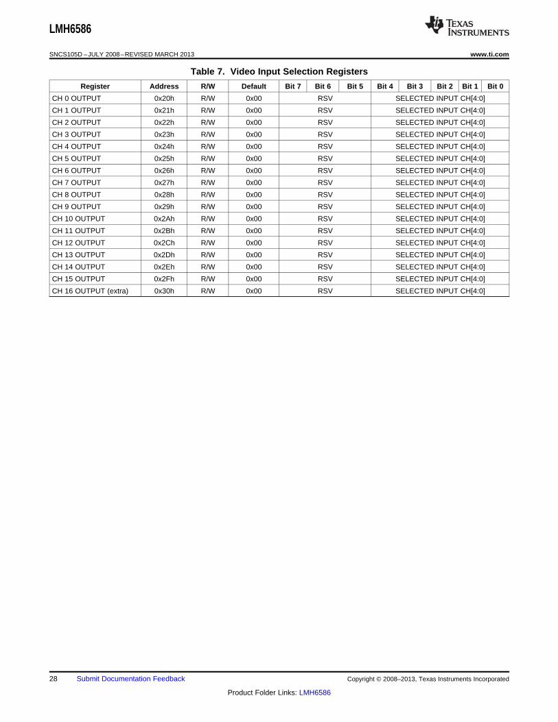
Video Input Selection Registers
Registers 0x20 to 0x30 are used to control the routing of the crosspoint switch. Each output has a dedicatedinput selection register, which can be programmed to select any input channel for routing to its respective output.
LMH6586 REGISTER MAP
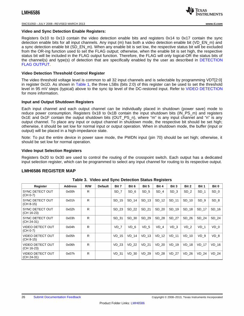
Table 3. Video and Sync Detection Status Registers
Register Address R/W Default Bit 7 Bit 6 Bit 5 Bit 4 Bit 3 Bit 2 Bit 1 Bit 0
SYNC DETECT OUT 0x00h R SD_7 SD_6 SD_5 SD_4 SD_3 SD_2 SD_1 SD_0(CH 0-7)
SYNC DETECT OUT 0x01h R SD_15 SD_14 SD_13 SD_12 SD_11 SD_10 SD_9 SD_8(CH 8-15)
SYNC DETECT OUT 0x02h R SD_23 SD_22 SD_21 SD_20 SD_19 SD_18 SD_17 SD_16(CH 16-23)
SYNC DETECT OUT 0x03h R SD_31 SD_30 SD_29 SD_28 SD_27 SD_26 SD_24 SD_24(CH 24-31)
VIDEO DETECT OUT 0x04h R VD_7 VD_6 VD_5 VD_4 VD_3 VD_2 VD_1 VD_0(CH 0-7)
VIDEO DETECT OUT 0x05h R VD_15 VD_14 VD_13 VD_12 VD_11 VD_10 VD_9 VD_8(CH 8-15)
VIDEO DETECT OUT 0x06h R VD_23 VD_22 VD_21 VD_20 VD_19 VD_18 VD_17 VD_16(CH 16-23)
VIDEO DETECT OUT 0x07h R VD_31 VD_30 VD_29 VD_28 VD_27 VD_26 VD_24 VD_24(CH 24-31)
26 Submit Documentation Feedback Copyright © 2008–2013, Texas Instruments Incorporated
Product Folder Links: LMH6586

LMH6586
www.ti.com SNCS105D –JULY 2008–REVISED MARCH 2013
Table 4. Video and Sync Detection Control Registers
Register Address R/W Default Bit 7 Bit 6 Bit 5 Bit 4 Bit 3 Bit 2 Bit 1 Bit 0
RESERVED 0x08h R/W 0x00 RSV RSV RSV RSV RSV RSV RSV RSV0x0Bh
VIDEO DETECT 0x0Ch R/W 0x00 VD_ VD_ VD_ VD_ VD_ VD_ VD_ VD_INVERT (CH 0-7) INV_7 INV_6 INV_5 INV_4 INV_3 INV_2 INV_1 INV_0
VIDEO DETECT 0x0Dh R/W 0x00 VD_ VD_ VD_ VD_ VD_ VD_ VD_ VD_INVERT (CH 8-15) INV_15 INV_14 INV_13 INV_12 INV_11 INV_10 INV_9 INV_8
VIDEO DETECT 0x0Eh R/W 0x00 VD_ VD_ VD_ VD_ VD_ VD_ VD_ VD_INVERT (CH 16-23) INV_23 INV_22 INV_21 INV_20 INV_19 INV_18 INV_17 INV_16
VIDEO DETECT 0x0Fh R/W 0x00 VD_ VD_ VD_ VD_ VD_ VD_ VD_ VD_INVERT (CH 24-31) INV_31 INV_30 INV_29 INV_28 INV_27 INV_26 INV_24 INV_24
SYNC DETECT 0x10h R/W 0x00 SD_ SD_ SD_ SD_ SD_ SD_ SD_ SD_ENABLE (CH 0-7) EN_7 EN_6 EN_5 EN_4 EN_3 EN_2 EN_1 EN_0
SYNC DETECT 0x11h R/W 0x00 SD_ SD_ SD_ SD_ SD_ SD_ SD_ SD_ENABLE (CH 8-15) EN_15 EN_14 EN_13 EN_12 EN_11 EN_10 EN_9 EN_8
SYNC DETECT 0x12h R/W 0x00 SD_ SD_ SD_ SD_ SD_ SD_ SD_ SD_ENABLE (CH 16-23) EN_23 EN_22 EN_21 EN_20 EN_19 EN_18 EN_17 EN_16
SYNC DETECT 0x13h R/W 0x00 SD_ SD_ SD_ SD_ SD_ SD_ SD_ SD_ENABLE (CH 24-31) EN_31 EN_30 EN_29 EN_28 EN_27 EN_26 EN_25 EN_24
VIDEO DETECT 0x14h R/W 0x00 VD_ VD_ VD_ VD_ VD_ VD_ VD_ VD_ENABLE (CH 0-7) EN_7 EN_6 EN_5 EN_4 EN_3 EN_2 EN_1 EN_0
VIDEO DETECT 0x15h R/W 0x00 VD_ VD_ VD_ VD_ VD_ VD_ VD_ VD_ENABLE (CH 8-15) EN_15 EN_14 EN_13 EN_12 EN_11 EN_10 EN_9 EN_8
VIDEO DETECT 0x16h R/W 0x00 VD_ VD_ VD_ VD_ VD_ VD_ VD_ VD_ENABLE (CH 16-23) EN_23 EN_22 EN_21 EN_20 EN_19 EN_18 EN_17 EN_16
VIDEO DETECT 0x17h R/W 0x00 VD_ VD_ VD_ VD_ VD_ VD_ VD_ SD_ENABLE (CH 24-31) EN_31 EN_30 EN_29 EN_28 EN_27 EN_26 EN_25 EN_24
Table 5. Video Detection Threshold Control Registers
Register Address R/W Default Bit 7 Bit 6 Bit 5 Bit 4 Bit 3 Bit 2 Bit 1 Bit 0
VIDEO DETECT 0x1Dh R/W 0x00 RSV VDT[2:0]THRESHOLD
Table 6. Input and Output Shutdown Registers
Register Address R/W Default Bit 7 Bit 6 Bit 5 Bit 4 Bit 3 Bit 2 Bit 1 Bit 0
INPUT SHUTDOWN 0x18h R/W 0x00 IN_ IN_ IN_ IN_ IN_ IN_ IN_ IN_(CH 0-7) PS_7 PS_6 PS_5 PS_4 PS_3 PS_2 PS_1 PS_0
INPUT SHUTDOWN 0x19h R/W 0x00 IN_ IN_ IN_ IN_ IN_ IN_ IN_ IN_(CH 8-15) PS_15 PS_14 PS_13 PS_12 PS_11 PS_10 PS_9 PS_8
INPUT SHUTDOWN 0x1Ah R/W 0x00 IN_ IN_ IN_ IN_ IN_ IN_ IN_ IN_(CH 16-23) PS_23 PS_22 PS_21 PS_20 PS_19 PS_18 PS_17 PS_16
INPUT SHUTDOWN 0x1Bh R/W 0x00 IN_ IN_ IN_ IN_ IN_ IN_ IN_ IN_(CH 24-31) PS_31 PS_30 PS_29 PS_28 PS_27 PS_26 PS_25 PS_24
OUTPUT 0x1Eh R/W 0x00 OUT_ OUT_ OUT_ OUT_ OUT_ OUT_ OUT_ OUT_SHUTDOWN PS_7 PS_6 PS_5 PS_4 PS_3 PS_2 PS_1 PS_0(CH 0-7)
OUTPUT 0x1Fh R/W 0x00 OUT_ OUT_ OUT_ OUT_ OUT_ OUT_ OUT_ OUT_SHUTDOWN PS_15 PS_14 PS_13 PS_12 PS_11 PS_10 PS_9 PS_8(CH 8-15)
Copyright © 2008–2013, Texas Instruments Incorporated Submit Documentation Feedback 27
Product Folder Links: LMH6586
LMH6586
SNCS105D –JULY 2008–REVISED MARCH 2013 www.ti.com
Table 7. Video Input Selection Registers
Register Address R/W Default Bit 7 Bit 6 Bit 5 Bit 4 Bit 3 Bit 2 Bit 1 Bit 0
CH 0 OUTPUT 0x20h R/W 0x00 RSV SELECTED INPUT CH[4:0]
CH 1 OUTPUT 0x21h R/W 0x00 RSV SELECTED INPUT CH[4:0]
CH 2 OUTPUT 0x22h R/W 0x00 RSV SELECTED INPUT CH[4:0]
CH 3 OUTPUT 0x23h R/W 0x00 RSV SELECTED INPUT CH[4:0]
CH 4 OUTPUT 0x24h R/W 0x00 RSV SELECTED INPUT CH[4:0]
CH 5 OUTPUT 0x25h R/W 0x00 RSV SELECTED INPUT CH[4:0]
CH 6 OUTPUT 0x26h R/W 0x00 RSV SELECTED INPUT CH[4:0]
CH 7 OUTPUT 0x27h R/W 0x00 RSV SELECTED INPUT CH[4:0]
CH 8 OUTPUT 0x28h R/W 0x00 RSV SELECTED INPUT CH[4:0]
CH 9 OUTPUT 0x29h R/W 0x00 RSV SELECTED INPUT CH[4:0]
CH 10 OUTPUT 0x2Ah R/W 0x00 RSV SELECTED INPUT CH[4:0]
CH 11 OUTPUT 0x2Bh R/W 0x00 RSV SELECTED INPUT CH[4:0]
CH 12 OUTPUT 0x2Ch R/W 0x00 RSV SELECTED INPUT CH[4:0]
CH 13 OUTPUT 0x2Dh R/W 0x00 RSV SELECTED INPUT CH[4:0]
CH 14 OUTPUT 0x2Eh R/W 0x00 RSV SELECTED INPUT CH[4:0]
CH 15 OUTPUT 0x2Fh R/W 0x00 RSV SELECTED INPUT CH[4:0]
CH 16 OUTPUT (extra) 0x30h R/W 0x00 RSV SELECTED INPUT CH[4:0]
28 Submit Documentation Feedback Copyright © 2008–2013, Texas Instruments Incorporated
Product Folder Links: LMH6586

LMH6586
www.ti.com SNCS105D –JULY 2008–REVISED MARCH 2013
REVISION HISTORY
Changes from Revision C (March 2013) to Revision D Page
• Changed layout of National Data Sheet to TI format .......................................................................................................... 26
Copyright © 2008–2013, Texas Instruments Incorporated Submit Documentation Feedback 29
Product Folder Links: LMH6586
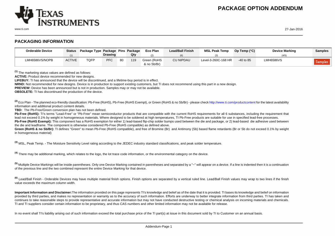
PACKAGE OPTION ADDENDUM
www.ti.com 27-Jan-2016
Addendum-Page 1
PACKAGING INFORMATION
Orderable Device Status(1)
Package Type PackageDrawing
Pins PackageQty
Eco Plan(2)
Lead/Ball Finish(6)
MSL Peak Temp(3)
Op Temp (°C) Device Marking(4/5)
Samples
LMH6586VS/NOPB ACTIVE TQFP PFC 80 119 Green (RoHS& no Sb/Br)
CU NIPDAU Level-3-260C-168 HR -40 to 85 LMH6586VS
(1) The marketing status values are defined as follows:ACTIVE: Product device recommended for new designs.LIFEBUY: TI has announced that the device will be discontinued, and a lifetime-buy period is in effect.NRND: Not recommended for new designs. Device is in production to support existing customers, but TI does not recommend using this part in a new design.PREVIEW: Device has been announced but is not in production. Samples may or may not be available.OBSOLETE: TI has discontinued the production of the device.
(2) Eco Plan - The planned eco-friendly classification: Pb-Free (RoHS), Pb-Free (RoHS Exempt), or Green (RoHS & no Sb/Br) - please check http://www.ti.com/productcontent for the latest availabilityinformation and additional product content details.TBD: The Pb-Free/Green conversion plan has not been defined.Pb-Free (RoHS): TI's terms "Lead-Free" or "Pb-Free" mean semiconductor products that are compatible with the current RoHS requirements for all 6 substances, including the requirement thatlead not exceed 0.1% by weight in homogeneous materials. Where designed to be soldered at high temperatures, TI Pb-Free products are suitable for use in specified lead-free processes.Pb-Free (RoHS Exempt): This component has a RoHS exemption for either 1) lead-based flip-chip solder bumps used between the die and package, or 2) lead-based die adhesive used betweenthe die and leadframe. The component is otherwise considered Pb-Free (RoHS compatible) as defined above.Green (RoHS & no Sb/Br): TI defines "Green" to mean Pb-Free (RoHS compatible), and free of Bromine (Br) and Antimony (Sb) based flame retardants (Br or Sb do not exceed 0.1% by weightin homogeneous material)
(3) MSL, Peak Temp. - The Moisture Sensitivity Level rating according to the JEDEC industry standard classifications, and peak solder temperature.
(4) There may be additional marking, which relates to the logo, the lot trace code information, or the environmental category on the device.
(5) Multiple Device Markings will be inside parentheses. Only one Device Marking contained in parentheses and separated by a "~" will appear on a device. If a line is indented then it is a continuationof the previous line and the two combined represent the entire Device Marking for that device.
(6) Lead/Ball Finish - Orderable Devices may have multiple material finish options. Finish options are separated by a vertical ruled line. Lead/Ball Finish values may wrap to two lines if the finishvalue exceeds the maximum column width.
Important Information and Disclaimer:The information provided on this page represents TI's knowledge and belief as of the date that it is provided. TI bases its knowledge and belief on informationprovided by third parties, and makes no representation or warranty as to the accuracy of such information. Efforts are underway to better integrate information from third parties. TI has taken andcontinues to take reasonable steps to provide representative and accurate information but may not have conducted destructive testing or chemical analysis on incoming materials and chemicals.TI and TI suppliers consider certain information to be proprietary, and thus CAS numbers and other limited information may not be available for release.
In no event shall TI's liability arising out of such information exceed the total purchase price of the TI part(s) at issue in this document sold by TI to Customer on an annual basis.
PACKAGE OPTION ADDENDUM
www.ti.com 27-Jan-2016
Addendum-Page 2
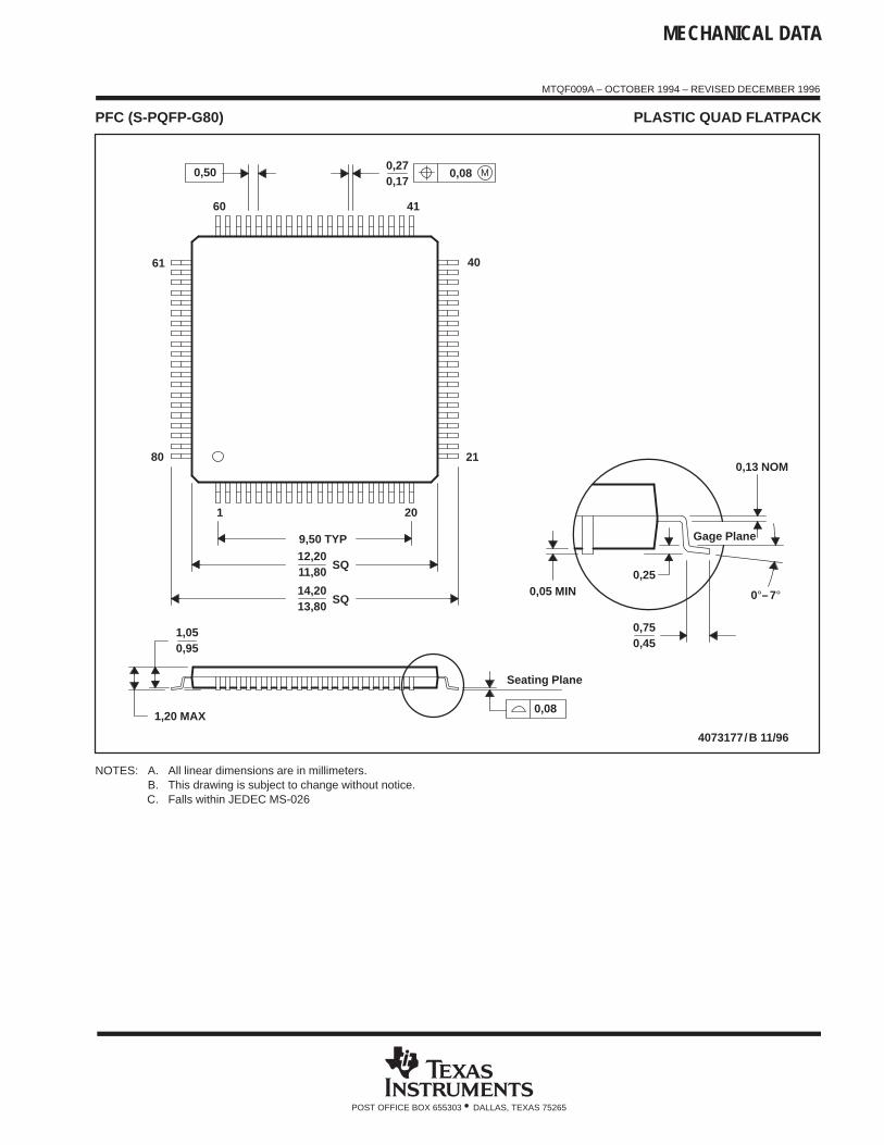
MECHANICAL DATA
MTQF009A – OCTOBER 1994 – REVISED DECEMBER 1996
POST OFFICE BOX 655303 • DALLAS, TEXAS 75265
PFC (S-PQFP-G80) PLASTIC QUAD FLATPACK
4073177/B 11/96
40
210,13 NOM
0,25
0,750,45
Seating Plane
0,05 MIN
Gage Plane
0,27
41
0,17
20
60
1
61
80
SQ
SQ
12,20
13,8014,20
11,80
9,50 TYP
1,05
1,20 MAX
0,95
0,08
0,50 M0,08
0°–7°
NOTES: A. All linear dimensions are in millimeters.B. This drawing is subject to change without notice.C. Falls within JEDEC MS-026

IMPORTANT NOTICE
Texas Instruments Incorporated and its subsidiaries (TI) reserve the right to make corrections, enhancements, improvements and otherchanges to its semiconductor products and services per JESD46, latest issue, and to discontinue any product or service per JESD48, latestissue. Buyers should obtain the latest relevant information before placing orders and should verify that such information is current andcomplete. All semiconductor products (also referred to herein as “components”) are sold subject to TI’s terms and conditions of salesupplied at the time of order acknowledgment.TI warrants performance of its components to the specifications applicable at the time of sale, in accordance with the warranty in TI’s termsand conditions of sale of semiconductor products. Testing and other quality control techniques are used to the extent TI deems necessaryto support this warranty. Except where mandated by applicable law, testing of all parameters of each component is not necessarilyperformed.TI assumes no liability for applications assistance or the design of Buyers’ products. Buyers are responsible for their products andapplications using TI components. To minimize the risks associated with Buyers’ products and applications, Buyers should provideadequate design and operating safeguards.TI does not warrant or represent that any license, either express or implied, is granted under any patent right, copyright, mask work right, orother intellectual property right relating to any combination, machine, or process in which TI components or services are used. Informationpublished by TI regarding third-party products or services does not constitute a license to use such products or services or a warranty orendorsement thereof. Use of such information may require a license from a third party under the patents or other intellectual property of thethird party, or a license from TI under the patents or other intellectual property of TI.Reproduction of significant portions of TI information in TI data books or data sheets is permissible only if reproduction is without alterationand is accompanied by all associated warranties, conditions, limitations, and notices. TI is not responsible or liable for such altereddocumentation. Information of third parties may be subject to additional restrictions.Resale of TI components or services with statements different from or beyond the parameters stated by TI for that component or servicevoids all express and any implied warranties for the associated TI component or service and is an unfair and deceptive business practice.TI is not responsible or liable for any such statements.Buyer acknowledges and agrees that it is solely responsible for compliance with all legal, regulatory and safety-related requirementsconcerning its products, and any use of TI components in its applications, notwithstanding any applications-related information or supportthat may be provided by TI. Buyer represents and agrees that it has all the necessary expertise to create and implement safeguards whichanticipate dangerous consequences of failures, monitor failures and their consequences, lessen the likelihood of failures that might causeharm and take appropriate remedial actions. Buyer will fully indemnify TI and its representatives against any damages arising out of the useof any TI components in safety-critical applications.In some cases, TI components may be promoted specifically to facilitate safety-related applications. With such components, TI’s goal is tohelp enable customers to design and create their own end-product solutions that meet applicable functional safety standards andrequirements. Nonetheless, such components are subject to these terms.No TI components are authorized for use in FDA Class III (or similar life-critical medical equipment) unless authorized officers of the partieshave executed a special agreement specifically governing such use.Only those TI components which TI has specifically designated as military grade or “enhanced plastic” are designed and intended for use inmilitary/aerospace applications or environments. Buyer acknowledges and agrees that any military or aerospace use of TI componentswhich have not been so designated is solely at the Buyer's risk, and that Buyer is solely responsible for compliance with all legal andregulatory requirements in connection with such use.TI has specifically designated certain components as meeting ISO/TS16949 requirements, mainly for automotive use. In any case of use ofnon-designated products, TI will not be responsible for any failure to meet ISO/TS16949.
Products ApplicationsAudio www.ti.com/audio Automotive and Transportation www.ti.com/automotiveAmplifiers amplifier.ti.com Communications and Telecom www.ti.com/communicationsData Converters dataconverter.ti.com Computers and Peripherals www.ti.com/computersDLP® Products www.dlp.com Consumer Electronics www.ti.com/consumer-appsDSP dsp.ti.com Energy and Lighting www.ti.com/energyClocks and Timers www.ti.com/clocks Industrial www.ti.com/industrialInterface interface.ti.com Medical www.ti.com/medicalLogic logic.ti.com Security www.ti.com/securityPower Mgmt power.ti.com Space, Avionics and Defense www.ti.com/space-avionics-defenseMicrocontrollers microcontroller.ti.com Video and Imaging www.ti.com/videoRFID www.ti-rfid.comOMAP Applications Processors www.ti.com/omap TI E2E Community e2e.ti.comWireless Connectivity www.ti.com/wirelessconnectivity
Mailing Address: Texas Instruments, Post Office Box 655303, Dallas, Texas 75265Copyright © 2016, Texas Instruments Incorporated