LME49810 200V Audio Power Amplifier Driver with Baker ... · LME49810 200V Audio Power Amplifier...
20
LME49810 www.ti.com SNAS391C – MAY 2007 – REVISED APRIL 2013 LME49810 200V Audio Power Amplifier Driver with Baker Clamp Check for Samples: LME49810 1FEATURES DESCRIPTION The LME49810 is a high fidelity audio power amplifier 2• Very High Voltage Operation driver designed for demanding consumer and pro- • Output Clamp Logic Output audio applications. Amplifier output power may be • Thermal Shutdown and Mute scaled by changing the supply voltage and number of power transistors. The LME49810’s minimum output • Customizable External Compensation current is 50mA. When using a discrete output stage • Scalable Output Power the LME49810 is capable of delivering in excess of 300 watts into a single-ended 8Ω load. APPLICATIONS Unique to the LME49810 is an internal Baker Clamp. • Guitar Amplifiers This clamp insures that the amplifier output does not • Powered Studio Monitors saturate when over driven. The resultant “soft clipping” of high level audio signals suppresses • Powered Subwoofers undesirable audio artifacts generated when • Pro Audio conventional solid state amplifiers are driven hard into • Audio Video Receivers clipping. • High Voltage Industrial Applications The LME49810 includes thermal shutdown circuitry that activates when the die temperature exceeds KEY SPECIFICATIONS 150°C. The LME49810’s mute function, when activated, mutes the input drive signal and forces the • Wide operating voltage range: ±20V to ±100V amplifier output to a quiescent state. • Slew Rate: 50V/μs (Typ) • Output Drive Current: 60mA (Typ) • PSRR (f = DC): 110dB (Typ) • THD+N (f = 1kHz): 0.0007 (Typ) 1 Please be aware that an important notice concerning availability, standard warranty, and use in critical applications of Texas Instruments semiconductor products and disclaimers thereto appears at the end of this data sheet. 2All trademarks are the property of their respective owners. PRODUCTION DATA information is current as of publication date. Copyright © 2007–2013, Texas Instruments Incorporated Products conform to specifications per the terms of the Texas Instruments standard warranty. Production processing does not necessarily include testing of all parameters.
Transcript of LME49810 200V Audio Power Amplifier Driver with Baker ... · LME49810 200V Audio Power Amplifier...
LME49810
www.ti.com SNAS391C –MAY 2007–REVISED APRIL 2013
LME49810 200V Audio Power Amplifier Driver with Baker ClampCheck for Samples: LME49810
1FEATURES DESCRIPTIONThe LME49810 is a high fidelity audio power amplifier
2• Very High Voltage Operationdriver designed for demanding consumer and pro-
• Output Clamp Logic Output audio applications. Amplifier output power may be• Thermal Shutdown and Mute scaled by changing the supply voltage and number of
power transistors. The LME49810’s minimum output• Customizable External Compensationcurrent is 50mA. When using a discrete output stage• Scalable Output Power the LME49810 is capable of delivering in excess of300 watts into a single-ended 8Ω load.
APPLICATIONSUnique to the LME49810 is an internal Baker Clamp.
• Guitar Amplifiers This clamp insures that the amplifier output does not• Powered Studio Monitors saturate when over driven. The resultant “soft
clipping” of high level audio signals suppresses• Powered Subwoofersundesirable audio artifacts generated when• Pro Audio conventional solid state amplifiers are driven hard into
• Audio Video Receivers clipping.• High Voltage Industrial Applications The LME49810 includes thermal shutdown circuitry
that activates when the die temperature exceedsKEY SPECIFICATIONS 150°C. The LME49810’s mute function, when
activated, mutes the input drive signal and forces the• Wide operating voltage range: ±20V to ±100Vamplifier output to a quiescent state.
• Slew Rate: 50V/μs (Typ)• Output Drive Current: 60mA (Typ)• PSRR (f = DC): 110dB (Typ)• THD+N (f = 1kHz): 0.0007 (Typ)
1
Please be aware that an important notice concerning availability, standard warranty, and use in critical applications ofTexas Instruments semiconductor products and disclaimers thereto appears at the end of this data sheet.
2All trademarks are the property of their respective owners.
PRODUCTION DATA information is current as of publication date. Copyright © 2007–2013, Texas Instruments IncorporatedProducts conform to specifications per the terms of the TexasInstruments standard warranty. Production processing does notnecessarily include testing of all parameters.

1234
567
89
1011
12
13
14
15
ClpFlagMute
GNDIN+IN-CompNCOsenseNC
BiasM
BiasP
Sink
Source
+VCC
-VEE
RE10.25
RE20.25
VCC
Audio Input
+
-
RF6.81 k
VCC
VEE-
+
+
VEE-
RL
8
RS6.81 k
CIN10
CS 0.1
Baker Circuitry and
Clip Flag
Source
Sink
IN+
IN-
Comp
BiasP
BiasM
5V+
Mute
+
+
CC 10 pF
Clpflag
RIN243
QMULT
RB21.21 k
RM33 k
Osense
Q1
RSB2.2 k
GNDLED
Mute Control
Ci220
Ri243
CS 0.1
RP200
Q2
Q3
Q4
+ 5V
RC470
PF
PF
:
:
:
RB1348
::
:
:
:
:
:
:
PF
PF
:
:
LME49810
SNAS391C –MAY 2007–REVISED APRIL 2013 www.ti.com
Typical Application
Figure 1. LME49810 Audio Amplifier Schematic
Connection Diagram
Figure 2. 15-Pin PFM (Top View)See NDN0015A Package
2 Submit Documentation Feedback Copyright © 2007–2013, Texas Instruments Incorporated
Product Folder Links: LME49810
Source
Sink
BiasP
Comp
IN+
IN-
-VEE
GND
Mute
BiasM
BakerClamp
BakerClamp
MuteControl
Osense
10k
Referenceand
Protection
ClpFlag +VCC
10k
50k 12.5k
GmAmp
GmAmp
LME49810
www.ti.com SNAS391C –MAY 2007–REVISED APRIL 2013
PIN DESCRIPTIONSPin Pin Name Description
1 ClpFlag Baker Clamp Clip Flag Output
2 Mute Mute Control
3 GND Device Ground
4 IN+ Non-Inverting Input
5 IN– Inverting Input
6 Comp External Compensation Connection
7 NC No Connect, Pin electrically isolated
8 Osense Output Sense
9 NC No Connect, Pin electrically isolated
10 –VEE Negative Power Supply
11 BiasM Negative External Bias Control
12 BiasP Positive External Bias Control
13 Sink Output Sink
14 Source Output Source
15 +VCC Positive Power Supply
Figure 3. LME49810 Simplified Schematic
These devices have limited built-in ESD protection. The leads should be shorted together or the device placed in conductive foamduring storage or handling to prevent electrostatic damage to the MOS gates.
Copyright © 2007–2013, Texas Instruments Incorporated Submit Documentation Feedback 3
Product Folder Links: LME49810

LME49810
SNAS391C –MAY 2007–REVISED APRIL 2013 www.ti.com
ABSOLUTE MAXIMUM RATINGS (1) (2) (3)
Supply Voltage |V+| + |V-| 200V
Differential Input Voltage ±6V
Common Mode Input Range 0.4VEE to 0.4VCC
Power Dissipation (4) 4W
ESD Susceptibility (5) 1kV
ESD Susceptibility (6) 200V
Junction Temperature (TJMAX) (7) 150°C
Soldering Information PFM Package (10 seconds) 260°C
Storage Temperature –40°C to +150°C
Thermal Resistance θJA 73°C/W
θJC 4°C/W
(1) All voltages are measured with respect to the GND pin unless otherwise specified.(2) Absolute Maximum Ratings indicate limits beyond which damage to the device may occur. Operating Ratings indicate conditions for
which the device is functional but do not ensure specific performance limits. Electrical Characteristics state DC and AC electricalspecifications under particular test conditions which ensure specific performance limits. This assumes that the device is within theOperating Ratings. Specifications are not for parameters where no limit is given, however, the typical value is a good indication of deviceperformance.
(3) If Military/Aerospace specified devices are required, please contact the Texas Instruments Sales Office/ Distributors for availability andspecifications.
(4) The maximum power dissipation must be derated at elevated temperatures and is dictated by TJMAX, θJC, and the ambient temperature,TA. The maximum allowable power dissipation is PDMAX = (TJMAX - TA) / θJC or the number given in Absolute Maximum Ratings,whichever is lower. For the LME49810, TJMAX = 150°C and the typical θJC is 4°C/W.
(5) Human body model, 100pF discharged through a 1.5kΩ resistor.(6) Machine Model, 220pF - 240pF discharged through all pins.(7) The maximum operating junction temperature is 150°C.
OPERATING RATINGSTemperature Range TMIN ≤ TA ≤ TMAX −40°C ≤ TA ≤ +8 5°C
Supply Voltage ±20V ≤ VSUPPLY ≤ ±100V
ELECTRICAL CHARACTERISTICS VCC = +100V, VEE = –100V (1) (2)
The following specifications apply for IMUTE = 100μA, unless otherwise specified. Limits apply for TA = 25°C, CC = 10pF, andAV = 29dB.
LME49810 UnitsSymbol Parameter Conditions (Limits)Typical (3) Limits (4) (5)
ICC Quiescent Power Supply Current VCM = 0V, VO = 0V, IO = 0A 11 18 mA (max)
IEE Quiescent Power Supply Current VCM = 0V, VO = 0V, IO = 0A 13 mA (max)
No Load, BW = 30kHz, VOUT = 30VRMS,THD+N Total Harmonic Distortion + Noise 0.0007 % (max)f = 1kHz
f = DC 120 dBAV Open Loop Gain f = 1kHz, VIN = 1mVRMS 88 dB
VOM Output Voltage Swing THD+N = 0.05%, f = 1kHz 67.5 V RMS
BW = 30kHz, 50 μVVNOISE Output Noise A-weighted 34 150 μV (max)
IOUT Output Current Current from Source to Sink Pins 60 50 mA (min)
50 μA (min)IMUTE Current into Mute Pin To activate the amplifier 100 200 μA (max)
(1) All voltages are measured with respect to the GND pin unless otherwise specified.(2) Absolute Maximum Ratings indicate limits beyond which damage to the device may occur. Operating Ratings indicate conditions for
which the device is functional but do not ensure specific performance limits. Electrical Characteristics state DC and AC electricalspecifications under particular test conditions which ensure specific performance limits. This assumes that the device is within theOperating Ratings. Specifications are not for parameters where no limit is given, however, the typical value is a good indication of deviceperformance.
(3) Typicals are measured at +25°C and represent the parametric norm.(4) Limits are specified to AOQL (Average Outgoing Quality Level).(5) Data sheet min and max specification limits are specified by design, test, or statistical analysis.
4 Submit Documentation Feedback Copyright © 2007–2013, Texas Instruments Incorporated
Product Folder Links: LME49810
+VCC
TEST SIGNAL
INPUT
Mute Control
+
-
RF6.81 k:
-VEE
RS6.81 k:
Ri243:
Baker Circuitry and
Clip Flag
Source
Sink
IN+
IN-
Comp
BiasP
BiasM
+5V
Mute
CS1 0.1 PF
+
+
CC10 pF
Clpflag
RIN243:
RC1 k:
RM33 k:
Osense
GNDOUTPUT
R110:
R210:
CS2 0.1 PF
+5V
CIN 220 PF
Ci220 PF
LME49810
www.ti.com SNAS391C –MAY 2007–REVISED APRIL 2013
ELECTRICAL CHARACTERISTICS VCC = +100V, VEE = –100V(1)(2) (continued)The following specifications apply for IMUTE = 100μA, unless otherwise specified. Limits apply for TA = 25°C, CC = 10pF, andAV = 29dB.
LME49810 UnitsSymbol Parameter Conditions (Limits)Typical (3) Limits (4) (5)
SR Slew Rate VIN = 1VP-P, f = 10kHz square Wave 50 V/μs(min)
VOS Input Offset Voltage VCM = 0V, IO= 0mA 1 3 mV (max)
IB Input Bias Current VCM = 0V, IO= 0mA 100 200 nA (max)
PSRR Power Supply Rejection Ratio f = DC, Input Referred 110 105 dB (min)
Clip OutputVCLIP Baker Clamp Clipping Voltage Source pin 97.2 95.5 V (max)
Sink pin –96.4 –95.5 V (min)
VBC Baker Clamp Flag Output Voltage IFLAG = 4.7mA 0.4 V
VBA Bias P&M Pin Open Voltage BiasP - BiasM 10 V
IBIAS Bias Adjust Function Current 2.8 mA
Figure 4. LME49810 Test Circuit Schematic (DC Coupled)
Copyright © 2007–2013, Texas Instruments Incorporated Submit Documentation Feedback 5
Product Folder Links: LME49810

20 100 10k0.0001
0.001
0.1
1
10
TH
D+
N (
%)
FREQUENCY (Hz)
20k1k
0.01BW=80 kHz
BW=30 kHz
20 100 10k0.0001
0.001
0.1
1
10
TH
D+
N (
%)
FREQUENCY (Hz)
20k1k
0.01BW=80 kHz
BW=30 kHz
20 100 10k0.0001
0.001
0.1
1
10
TH
D+
N (
%)
FREQUENCY (Hz)
20k1k
0.01BW=80 kHz
BW=30 kHz
20 100 10k0.0001
0.001
0.1
1
10
TH
D+
N (
%)
FREQUENCY (Hz)
20k1k
0.01
BW=80 kHz
BW=30 kHz
20 100 10k0.0001
0.001
0.1
1
10
TH
D+
N (
%)
FREQUENCY (Hz)
20k1k
0.01BW=80 kHz
BW=30 kHz
20 100 10k0.0001
0.001
0.1
1
10
TH
D+
N (
%)
FREQUENCY (Hz)
20k1k
0.01BW=80 kHz
BW=30 kHz
LME49810
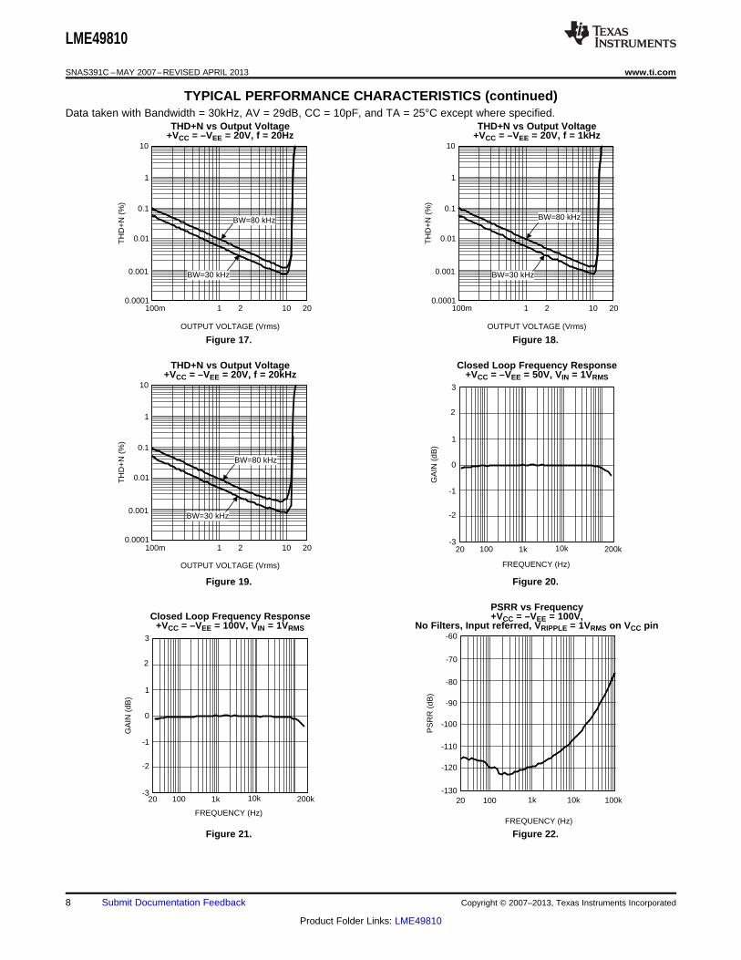
SNAS391C –MAY 2007–REVISED APRIL 2013 www.ti.com
TYPICAL PERFORMANCE CHARACTERISTICSData taken with Bandwidth = 30kHz, AV = 29dB, CC = 10pF, and TA = 25°C except where specified.
THD+N vs Frequency THD+N vs Frequency+VCC = –VEE = 20V, VO = 5V +VCC = –VEE = 20V, VO = 10V
Figure 5. Figure 6.
THD+N vs Frequency THD+N vs Frequency+VCC = –VEE = 50V, VO = 14V +VCC = –VEE = 50V, VO = 20V
Figure 7. Figure 8.
THD+N vs Frequency THD+N vs Frequency+VCC = –VEE = 100V, VO = 14V +VCC = –VEE = 50V, VO = 30V
Figure 9. Figure 10.
6 Submit Documentation Feedback Copyright © 2007–2013, Texas Instruments Incorporated
Product Folder Links: LME49810
100m 1 200.0001
0.001
0.1
1
10
TH
D+
N (
%)
OUTPUT VOLTAGE (Vrms)
50
0.01
102
BW=80 kHz
BW=30 kHz
TH
D+
N (
%)
100m 1 50
0.001
0.1
1
10
OUTPUT VOLTAGE (Vrms)
100
0.01
10
BW=80 kHz
BW=30 kHz
100m 1 200.0001
0.001
0.1
1
10
TH
D+
N (
%)
OUTPUT VOLTAGE (Vrms)
50
0.01
102
BW=80 kHz
BW=30 kHz
100m 1 500.0001
0.001
0.1
1
10
TH
D+
N (
%)
OUTPUT VOLTAGE (Vrms)
100
0.01
10
BW=30 kHz
BW=80 kHz
100m 1 200.0001
0.001
0.1
1
10
TH
D+
N (
%)
OUTPUT VOLTAGE (Vrms)
50
0.01
102
BW=80 kHz
BW=30 kHz
100m 1 500.0001
0.001
0.1
1
10
TH
D+
N (
%)
OUTPUT VOLTAGE (Vrms)
100
0.01
10
BW=30 kHz
BW=80 kHz
LME49810
www.ti.com SNAS391C –MAY 2007–REVISED APRIL 2013
TYPICAL PERFORMANCE CHARACTERISTICS (continued)Data taken with Bandwidth = 30kHz, AV = 29dB, CC = 10pF, and TA = 25°C except where specified.
THD+N vs Output Voltage THD+N vs Output Voltage+VCC = – VEE = 50V, f = 20Hz +VCC = –VEE = 100V, f = 20Hz
Figure 11. Figure 12.
THD+N vs Output Voltage THD+N vs Output Voltage+VCC = –VEE = 50V, f = 1kHz +VCC = – VEE = 100V, f = 1kHz
Figure 13. Figure 14.
THD+N vs Output Voltage THD+N vs Output Voltage+VCC = –VEE = 50V, f = 20kHz +VCC = –VEE = 100V, f = 20kHz
Figure 15. Figure 16.
Copyright © 2007–2013, Texas Instruments Incorporated Submit Documentation Feedback 7
Product Folder Links: LME49810
20 1k 10k 100k-130
-120
-100
-90
-80
-70
-60
PS
RR
(dB
)
FREQUENCY (Hz)
100
-110
20 100-3
-2
0
1
3
GA
IN (
dB)
FREQUENCY (Hz)
200k1k
-1
2
10k
20 100-3
-2
0
1
3
GA
IN (
dB)
FREQUENCY (Hz)
200k1k
-1
2
10k100m 1 100.0001
0.001
0.1
1
10
TH
D+
N (
%)
OUTPUT VOLTAGE (Vrms)
20
0.01
2
BW=80 kHz
BW=30 kHz
100m 1 100.0001
0.001
0.1
1
10
TH
D+
N (
%)
OUTPUT VOLTAGE (Vrms)
20
0.01
2
BW=80 kHz
BW=30 kHz
100m 1 100.0001
0.001
0.1
1
10
TH
D+
N (
%)
OUTPUT VOLTAGE (Vrms)
20
0.01
2
BW=80 kHz
BW=30 kHz
LME49810
SNAS391C –MAY 2007–REVISED APRIL 2013 www.ti.com
TYPICAL PERFORMANCE CHARACTERISTICS (continued)Data taken with Bandwidth = 30kHz, AV = 29dB, CC = 10pF, and TA = 25°C except where specified.
THD+N vs Output Voltage THD+N vs Output Voltage+VCC = –VEE = 20V, f = 20Hz +VCC = –VEE = 20V, f = 1kHz
Figure 17. Figure 18.
THD+N vs Output Voltage Closed Loop Frequency Response+VCC = –VEE = 20V, f = 20kHz +VCC = –VEE = 50V, VIN = 1VRMS
Figure 19. Figure 20.
PSRR vs FrequencyClosed Loop Frequency Response +VCC = –VEE = 100V,
+VCC = –VEE = 100V, VIN = 1VRMS No Filters, Input referred, VRIPPLE = 1VRMS on VCC pin
Figure 21. Figure 22.
8 Submit Documentation Feedback Copyright © 2007–2013, Texas Instruments Incorporated
Product Folder Links: LME49810

20 1200
1
2
7
INP
UT
OF
FS
ET
VO
LTA
GE
(m
V)
SUPPLY VOLTAGE (±V)
30 5040 60
3
4
5
70 80 90 100 110
6
20 1200
4
8
28
SU
PP
LY C
UR
RE
NT
(m
A)
SUPPLY VOTAGE (±V)
30 5040 60
12
16
20
70 80 90 100 110
24
ICC
IEE
0 20 30 600
10
30
40
50
60
70
SLE
W R
AT
E (
V/P
s)
COMPENSATION CAPACITOR (pF)
10
20
40 500 1000
40
80
100
OU
TP
UT
VO
TLA
GE
(V
RM
S)
SUPPLY VOLTAGE (±V)
20
60
60
20
40
THD+N = 0.05%
THD+N = 10%
80
20 1k 10k 100k-120
-100
-60
-40
-20
0
PS
RR
(dB
)
FREQUENCY (Hz)
100
-80
0.1 1k-140
-100
-60
-40
-20
0
20
MU
TE
AT
TE
NU
AT
ION
(dB
)
IMUTE (PA)
1
-80
100
-120
10
fIN = 20 kHz
fIN = 1 kHz
LME49810
www.ti.com SNAS391C –MAY 2007–REVISED APRIL 2013
TYPICAL PERFORMANCE CHARACTERISTICS (continued)Data taken with Bandwidth = 30kHz, AV = 29dB, CC = 10pF, and TA = 25°C except where specified.
PSRR vs Frequency+VCC = –VEE = 100V, Mute Attenuation vs IMUTE
No Filters, Input referred, VRIPPLE = 1VRMS on VEE pin +VCC = –VEE = 100V
Figure 23. Figure 24.
Slew Rate vs Compensation CapacitorOutput Voltage vs Supply Voltage +VCC = –VEE = 100V, VIN = 1.2VP 10kHz squarewave
Figure 25. Figure 26.
Supply Current vs Supply Voltage Input Offset Voltage vs Supply Voltage
Figure 27. Figure 28.
Copyright © 2007–2013, Texas Instruments Incorporated Submit Documentation Feedback 9
Product Folder Links: LME49810
20 100 10k10P
500P
1m
OU
TP
UT
NO
ISE
(V
RM
S)
FREQUENCY (Hz)
20k1k
100P
20P
50P
200P
BW=30 kHz
A-WEIGHTED
20 100 10k10P
500P
1m
OU
TP
UT
NO
ISE
(V
RM
S)
FREQUENCY (Hz)
20k1k
100PBW=30 kHz
A-WEIGHTED
20P
50P
200P
10 100M-20
20
60
80
200
GA
IN (
dB)
FREQUENCY (Hz)
100
40
10k
0
1k 100k
100
120
140
160
180
1M 10M-20
20
60
80
200
40
0
100
120
140
160
180
PH
AS
E M
AR
GIN
(o )
10 1M0
40
80
100
120
CM
RR
(dB
)
FREQUENCY (Hz)
100
60
10k
20
1k 100k
LME49810
SNAS391C –MAY 2007–REVISED APRIL 2013 www.ti.com
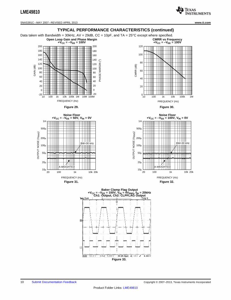
TYPICAL PERFORMANCE CHARACTERISTICS (continued)Data taken with Bandwidth = 30kHz, AV = 29dB, CC = 10pF, and TA = 25°C except where specified.
Open Loop Gain and Phase Margin CMRR vs Frequency+VCC = –VEE = 100V +VCC = –VEE = 100V
Figure 29. Figure 30.
Noise Floor Noise Floor+VCC = –VEE = 50V, VIN = 0V +VCC = –VEE = 100V, VIN = 0V
Figure 31. Figure 32.
Baker Clamp Flag Output+VCC = –VEE = 100V, VIN = 4VRMS, fIN = 20kHz
Ch1: Output, Ch2: CLPFLAG Output
Figure 33.
10 Submit Documentation Feedback Copyright © 2007–2013, Texas Instruments Incorporated
Product Folder Links: LME49810

LME49810
www.ti.com SNAS391C –MAY 2007–REVISED APRIL 2013
APPLICATION INFORMATION
MUTE FUNCTION
The mute function of the LME49810 is controlled by the amount of current that flows into the MUTE pin.LME49810 typically requires 50μA to 100μA of mute current flowing in order to be in “play” mode. This can bedone by connecting a reference voltage (VMUTE) to the MUTE pin through a resistor (RM). The following formulacan be used to calculate the mute current.
IMUTE = (VMUTE-0.7V) / (RM+10kΩ) (A) (1)
The 10kΩ resistor value in Equation (1) is internal. Please refer to Figure 3, LME49810 Simplified Schematic, foradditional details. For example, if a 5V voltage is connected through a 33kΩ resistor to the MUTE pin, then themute current will be 100μA, according to Equation (1). Consequently, RM can be changed to suit any otherreference voltage requirement. The LME49810 will enter Mute mode if IMUTE is less than 1μA which can beaccomplished by shorting the MUTE pin to ground or by floating the MUTE pin. It is not recommended that morethan 200μA flow into the MUTE pin because damage to LME49810 may occur and device may not functionproperly.
BAKER CLAMP AND CLAMP FLAG OUTPUT
The LME49810 features a Baker Clamp function with corresponding CLPFLAG output pin. The clamp functionkeeps all transistors in linear operation when the output goes into clipping. In addition, when the output goes intoclipping, a logic low level appears at the CLPFLAG pin. The CLPFLGAG pin can be used to drive an LED orsome other visual display as shown by Figure 1. The value of logic low voltage varies and depends on IFLAG. Forexample, if IFLAG is 4.7mA then a voltage (VBC) of 0.4V will appear at the CLPFLAG output pin. The smoothresponse of the Baker Clamp and the corresponding CLPFLAG logic output is shown in the scope photo below:
+VCC = -VEE = 100V,VIN = 4VRMS,fIN = 1kHz,RC = 1kΩ Ch1: Output,Ch2: CLPFLAG Output
Figure 34.
The CLPFLAG pin can source up to 10mA, and since the CLPFLAG output is an open collector output as shownby Figure 3, LME49810 Simplified Schematic, it should never be left to float under normal operation. If CLPFLAGpin is not used, then it should be connected through a resistor to a reference voltage so that IFLAG is below10mA. For example, a resistor of 1k can be used with a 5V reference voltage. This will give the IFLAG of 4.7mA. Ina typical LED setup, if +5V reference voltage is not available, the following circuit using a Zener diode can beused to power the CLPFLAG pin from the higher supply voltage rails of the LME49810. The power dissipationrating of RZ will need to be at-least ½W if using a 5V Zener Diode. Alternately, the following basic formula can beused to find the proper power rating of RZ : PDZ = (VCC - VZ)2/RZ (W). This formula can also be used to meet thedesign requirements of any other reference voltage that the user desires.
Copyright © 2007–2013, Texas Instruments Incorporated Submit Documentation Feedback 11
Product Folder Links: LME49810

50V-100VRM
470:TO CLPFLAG PIN
IN4733
RZ
22 k:
LME49810
SNAS391C –MAY 2007–REVISED APRIL 2013 www.ti.com
THERMAL PROTECTION
The LME49810 has a thermal protection scheme to prevent long-term thermal stress of the device. When thetemperature on the die exceeds 150°C, the LME49810 goes into thermal shutdown. The LME49810 startsoperating again when the die temperature drops to about 145°C, but if the temperature again begins to rise,shutdown will occur again above 150°C. Therefore, the device is allowed to heat up to a relatively hightemperature if the fault condition is temporary, but a sustained fault will cause the device to cycle between thethermal shutdown temperature limits of 150°C and 145°C. This greatly reduces the stress imposed on the IC bythermal cycling, which in turn improves its reliability under sustained fault conditions. Since the die temperature isdirectly dependent upon the heat sink used, the heat sink should be chosen so that thermal shutdown is notactivated during normal operation. Using the best heat sink possible within the cost and space constraints of thesystem will improve the long-term reliability of any power semiconductor device, as discussed in theDETERMINING THE CORRECT HEAT SINK section.
POWER DISSIPATION
When in “play” mode, the LME49810 draws a constant amount of current, regardless of the input signalamplitude. Consequently, the power dissipation is constant for a given supply voltage and can be computed withthe equation PDMAX = ICC * (VCC – VEE). For a quick calculation of PDMAX, approximate the current to be 11mAand multiply it by the total supply voltage (the current varies slightly from this value over the operating range).
DETERMINING THE CORRECT HEAT SINK
The choice of a heat sink for a high-power audio amplifier is made entirely to keep the die temperature at a levelsuch that the thermal protection circuitry is not activated under normal circumstances.
The thermal resistance from the die to the outside air, θJA (junction to ambient), is a combination of three thermalresistances, θJC (junction to case), θCS (case to sink), and θSA (sink to ambient). The thermal resistance, θJC(junction to case), of the LME49810 is 4°C/W. Using Thermalloy Thermacote thermal compound, the thermalresistance, θCS (case to sink), is about 0.2°C/W. Since convection heat flow (power dissipation) is analogous tocurrent flow, thermal resistance is analogous to electrical resistance, and temperature drops are analogous tovoltage drops, the power dissipation out of the LME49810 is equal to the following:
PDMAX = (TJMAX−TAMB) / θJA
where• TJMAX = 150°C• TAMB is the system ambient temperature• θJA = θJC + θCS + θSA (2)
12 Submit Documentation Feedback Copyright © 2007–2013, Texas Instruments Incorporated
Product Folder Links: LME49810

LME49810
www.ti.com SNAS391C –MAY 2007–REVISED APRIL 2013
Once the maximum package power dissipation has been calculated using Equation (2), the maximum thermalresistance, θSA, (heat sink to ambient) in °C/W for a heat sink can be calculated. This calculation is made usingEquation (3) which is derived by solving for θSA from Equation (2).
θSA = [(TJMAX−TAMB)−PDMAX(θJC +θCS)] / PDMAX (3)
Again it must be noted that the value of θSA is dependent upon the system designer's amplifier requirements. Ifthe ambient temperature that the audio amplifier is to be working under is higher than 25°C, then the thermalresistance for the heat sink, given all other things are equal, will need to be smaller.
PROPER SELECTION OF EXTERNAL COMPONENTS
Proper selection of external components is required to meet the design targets of an application. The choice ofexternal component values that will affect gain and low frequency response are discussed below.
The overall gain of the amplifier is set by resistors RF and Ri for the non-inverting configuration shown inFigure 1. The gain is found by Equation (4) below given Ri = RIN and RF = RS.
AV = RF / Ri (V/V) (4)
For best Noise performance, lower values of resistors are used. A value of 243 is commonly used for Ri andsetting the value for RF for desired gain. For the LME49810 the gain should be set no lower than 10V/V. Gainsettings below 10V/V may experience instability.
The combination of Ri and Ci (see Figure 1) creates a high pass filter. The gain at low frequency and thereforethe response is determined by these components. The -3dB point can be determined from Equation (5) shownbelow:
fi = 1 / (2πRiCi) (Hz) (5)
If an input coupling capacitor (CIN) is used to block DC from the inputs as shown in Figure 1, there will beanother high pass filter created with the combination of CIN and RIN. The resulting -3dB frequency response dueto the combination of CIN and RIN can be found from Equation (6) shown below:
fIN = 1 / (2πRINCIN) (Hz) (6)
For best audio performance, the input capacitor should not be used. Without the input capacitor, any DC biasfrom the source will be transferred to the load. The feedback capacitor (Ci) is used to set the gain at DC to unity.Because a large value is required for a low frequency -3dB point, the capacitor is an electrolytic type. Anadditional small value, high quality film capacitor may be used in parallel with the feedback resistor to improvehigh frequency sonic performance. If DC offset in the output stage is acceptable without the feedback capacitor,it may be removed but DC gain will now be equal to AC gain.
COMPENSATION CAPACITOR
The compensation capacitor (CC) is one of the most critical external components in value, placement and type.The capacitor should be placed close to the LME49810 and a silver mica type will give good performance. Thevalue of the capacitor will affect slew rate and stability. The highest slew rate is possible while also maintainingstability through out the power and frequency range of operation results in the best audio performance. The valueshown in Figure 1 should be considered a starting value with optimization done on the bench and in listeningtesting. Please refer to Slew Rate vs. CC Graph in TYPICAL PERFORMANCE CHARACTERISTICS fordetermining the proper slew rate for your particular application.
SUPPLY BYPASSING
The LME49810 has excellent power supply rejection and does not require a regulated supply. However, toeliminate possible oscillations all op amps and power op amps should have their supply leads bypassed with low-inductance capacitors having short leads and located close to the package terminals. Inadequate power supplybypassing will manifest itself by a low frequency oscillation known as “motorboating” or by high frequencyinstabilities. These instabilities can be eliminated through multiple bypassing utilizing a large electrolytic capacitor(10μF or larger) which is used to absorb low frequency variations and a small ceramic capacitor (0.1μF) toprevent any high frequency feedback through the power supply lines. If adequate bypassing is not provided thecurrent in the supply leads which is a rectified component of the load current may be fed back into internalcircuitry. This signal causes low distortion at high frequencies requiring that the supplies be bypassed at thepackage terminals with an electrolytic capacitor of 470μF or more.
Copyright © 2007–2013, Texas Instruments Incorporated Submit Documentation Feedback 13
Product Folder Links: LME49810

LME49810
SNAS391C –MAY 2007–REVISED APRIL 2013 www.ti.com
OUTPUT STAGE USING BIPOLAR TRANSISTORS
With a properly designed output stage and supply voltage of ±100V, an output power up to 500W can begenerated at 0.05% THD+N into an 8Ω speaker load. With an output current of several amperes, the outputtransistors need substantial base current drive because power transistors usually have quite low currentgain—typical hfe of 50 or so. To increase the current gain, audio amplifiers commonly use Darlington styledevices. Power transistors should be mounted together with the VBE multiplier transistor on the same heat sink toavoid thermal run away. Please see the section BIASING TECHNIQUES AND AVOIDING THERMALRUNAWAY for additional information.
BIASING TECHNIQUES AND AVOIDING THERMAL RUNAWAY
A class AB amplifier has some amount of distortion called Crossover distortion. To effectively minimize thecrossover distortion from the output, a VBE multiplier may be used instead of two biasing diodes. The LME49810has two dedicated pins (BIASM and BIASP) for Bias setup and provide a constant current source of about 2.8mA.A VBE multiplier normally consists of a bipolar transistor (QMULT, see Figure 1) and two resistors (RB1 and RB2,see Figure 1). A trim pot can also be added in series with RB1 for optional bias adjustment. A properly designedoutput stage, combine with a VBE multiplier, can eliminate the trim pot and virtually eliminate crossover distortion.The VCE voltage of QMULT (also called BIAS of the output stage) can be set by following formula:
VBIAS = VBE(1+RB2/RB1) (V) (7)
When using a bipolar output stage with the LME49810 (as in Figure 1), the designer must beware of thermalrunaway. Thermal runaway is a result of the temperature dependence of VBE (an inherent property of thetransistor). As temperature increases, VBE decreases. In practice, current flowing through a bipolar transistorheats up the transistor, which lowers the VBE. This in turn increases the current gain, and the cycle repeats. If thesystem is not designed properly this positive feedback mechanism can destroy the bipolar transistors used in theoutput stage. One of the recommended methods of preventing thermal runaway is to use the same heat sink onthe bipolar output stage transistor together with VBE multiplier transistor. When the VBE multiplier transistor ismounted to the same heat sink as the bipolar output stage transistors, it temperature will track that of the outputtransistors. Its VBE is dependent upon temperature as well, and so it will draw more current as the outputtransistors heat up, reducing the bias voltage to compensate. This will limit the base current into the outputtransistors, which counteracts thermal runaway. Another widely popular method of preventing thermal runaway isto use low value emitter degeneration resistors (RE1 and RE2). As current increases, the voltage at the emitteralso increases, which decreases the voltage across the base and emitter. This mechanism helps to limit thecurrent and counteracts thermal runaway.
LAYOUT CONSIDERATION AND AVOIDING GROUND LOOPS
A proper layout is virtually essential for a high performance audio amplifier. It is very important to return the loadground, supply grounds of output transistors, and the low level (feedback and input) grounds to the circuit boardcommon ground point through separate paths. When ground is routed in this fashion, it is called a star ground ora single point ground. It is advisable to keep the supply decoupling capacitors of 0.1μF close as possible toLME49810 to reduce the effects of PCB trace resistance and inductance. Following the general rules willoptimize the PCB layout and avoid ground loops problems:a. Make use of symmetrical placement of components.b. Make high current traces, such as output path traces, as wide as possible to accomodate output stage
current requirement.c. To reduce the PCB trace resistance and inductance, same ground returns paths should be as short as
possible. If possible, make the output traces short and equal in length.d. To reduce the PCB trace resistance and inductance, ground returns paths should be as short as possible.e. If possible, star ground or a single point ground should be observed. Advanced planning before starting the
PCB can improve audio performance.
14 Submit Documentation Feedback Copyright © 2007–2013, Texas Instruments Incorporated
Product Folder Links: LME49810
+VCC
TEST SIGNAL
INPUT
Mute Control
+
-
RF6.81 k:
-VEE
RS6.81 k:
Ri243:
Ci220 PF
Baker Circuitry and Clip
Flag
Source
Sink
IN+
IN-
Comp
BiasP
BiasM
+5V
Mute
CS1 0.1 PF
+
+
Cc10 pF
Clpflag
RIN243:
LEDRc
470:
RM33 k:
Osense
GNDOUTPUT
CIN 220 PF
R110:
R210:
J2
J1
RB10:
CS2 0.1 PF
+5V
LME49810
www.ti.com SNAS391C –MAY 2007–REVISED APRIL 2013
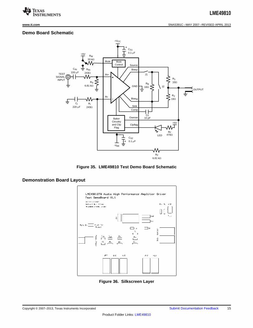
Demo Board Schematic
Figure 35. LME49810 Test Demo Board Schematic
Demonstration Board Layout
Figure 36. Silkscreen Layer
Copyright © 2007–2013, Texas Instruments Incorporated Submit Documentation Feedback 15
Product Folder Links: LME49810
LME49810
SNAS391C –MAY 2007–REVISED APRIL 2013 www.ti.com
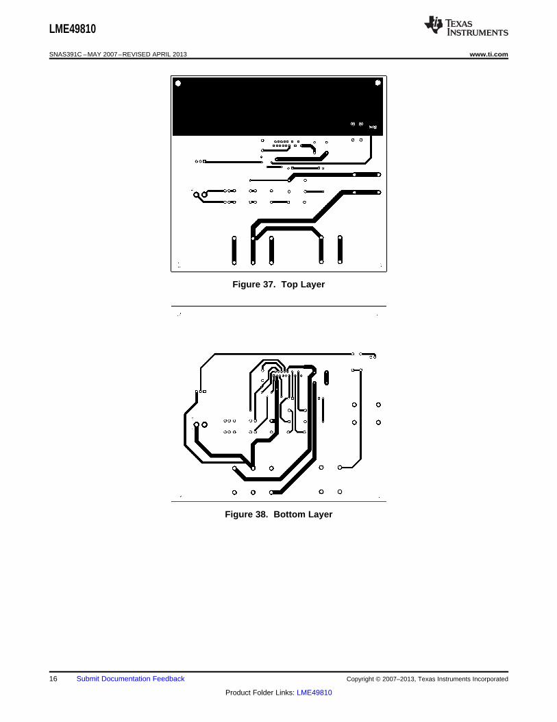
Figure 37. Top Layer
Figure 38. Bottom Layer
16 Submit Documentation Feedback Copyright © 2007–2013, Texas Instruments Incorporated
Product Folder Links: LME49810

LME49810
www.ti.com SNAS391C –MAY 2007–REVISED APRIL 2013
REVISION HISTORY
Rev Date Description
1.0 05/24/07 Initial WEB release.
1.01 05/29/07 Few text edits.
1.02 09/17/07 Edited curve 20216724.
C 04/05/13 Changed layout of National Data Sheet to TI format.
Copyright © 2007–2013, Texas Instruments Incorporated Submit Documentation Feedback 17
Product Folder Links: LME49810

PACKAGE OPTION ADDENDUM
www.ti.com 21-May-2013
Addendum-Page 1
PACKAGING INFORMATION
Orderable Device Status(1)
Package Type PackageDrawing
Pins PackageQty
Eco Plan(2)
Lead/Ball Finish MSL Peak Temp(3)
Op Temp (°C) Device Marking(4/5)
Samples
LME49810TB/NOPB ACTIVE TO-OTHER NDN 15 24 Green (RoHS& no Sb/Br)
CU SN Level-1-NA-UNLIM -20 to 85 LME49810TB
(1) The marketing status values are defined as follows:ACTIVE: Product device recommended for new designs.LIFEBUY: TI has announced that the device will be discontinued, and a lifetime-buy period is in effect.NRND: Not recommended for new designs. Device is in production to support existing customers, but TI does not recommend using this part in a new design.PREVIEW: Device has been announced but is not in production. Samples may or may not be available.OBSOLETE: TI has discontinued the production of the device.
(2) Eco Plan - The planned eco-friendly classification: Pb-Free (RoHS), Pb-Free (RoHS Exempt), or Green (RoHS & no Sb/Br) - please check http://www.ti.com/productcontent for the latest availabilityinformation and additional product content details.TBD: The Pb-Free/Green conversion plan has not been defined.Pb-Free (RoHS): TI's terms "Lead-Free" or "Pb-Free" mean semiconductor products that are compatible with the current RoHS requirements for all 6 substances, including the requirement thatlead not exceed 0.1% by weight in homogeneous materials. Where designed to be soldered at high temperatures, TI Pb-Free products are suitable for use in specified lead-free processes.Pb-Free (RoHS Exempt): This component has a RoHS exemption for either 1) lead-based flip-chip solder bumps used between the die and package, or 2) lead-based die adhesive used betweenthe die and leadframe. The component is otherwise considered Pb-Free (RoHS compatible) as defined above.Green (RoHS & no Sb/Br): TI defines "Green" to mean Pb-Free (RoHS compatible), and free of Bromine (Br) and Antimony (Sb) based flame retardants (Br or Sb do not exceed 0.1% by weightin homogeneous material)
(3) MSL, Peak Temp. -- The Moisture Sensitivity Level rating according to the JEDEC industry standard classifications, and peak solder temperature.
(4) There may be additional marking, which relates to the logo, the lot trace code information, or the environmental category on the device.
(5) Multiple Device Markings will be inside parentheses. Only one Device Marking contained in parentheses and separated by a "~" will appear on a device. If a line is indented then it is a continuationof the previous line and the two combined represent the entire Device Marking for that device.
Important Information and Disclaimer:The information provided on this page represents TI's knowledge and belief as of the date that it is provided. TI bases its knowledge and belief on informationprovided by third parties, and makes no representation or warranty as to the accuracy of such information. Efforts are underway to better integrate information from third parties. TI has taken andcontinues to take reasonable steps to provide representative and accurate information but may not have conducted destructive testing or chemical analysis on incoming materials and chemicals.TI and TI suppliers consider certain information to be proprietary, and thus CAS numbers and other limited information may not be available for release.
In no event shall TI's liability arising out of such information exceed the total purchase price of the TI part(s) at issue in this document sold by TI to Customer on an annual basis.

MECHANICAL DATA
NDN0015A
www.ti.com
TB15A (Rev A)
IMPORTANT NOTICE
Texas Instruments Incorporated and its subsidiaries (TI) reserve the right to make corrections, enhancements, improvements and otherchanges to its semiconductor products and services per JESD46, latest issue, and to discontinue any product or service per JESD48, latestissue. Buyers should obtain the latest relevant information before placing orders and should verify that such information is current andcomplete. All semiconductor products (also referred to herein as “components”) are sold subject to TI’s terms and conditions of salesupplied at the time of order acknowledgment.
TI warrants performance of its components to the specifications applicable at the time of sale, in accordance with the warranty in TI’s termsand conditions of sale of semiconductor products. Testing and other quality control techniques are used to the extent TI deems necessaryto support this warranty. Except where mandated by applicable law, testing of all parameters of each component is not necessarilyperformed.
TI assumes no liability for applications assistance or the design of Buyers’ products. Buyers are responsible for their products andapplications using TI components. To minimize the risks associated with Buyers’ products and applications, Buyers should provideadequate design and operating safeguards.
TI does not warrant or represent that any license, either express or implied, is granted under any patent right, copyright, mask work right, orother intellectual property right relating to any combination, machine, or process in which TI components or services are used. Informationpublished by TI regarding third-party products or services does not constitute a license to use such products or services or a warranty orendorsement thereof. Use of such information may require a license from a third party under the patents or other intellectual property of thethird party, or a license from TI under the patents or other intellectual property of TI.
Reproduction of significant portions of TI information in TI data books or data sheets is permissible only if reproduction is without alterationand is accompanied by all associated warranties, conditions, limitations, and notices. TI is not responsible or liable for such altereddocumentation. Information of third parties may be subject to additional restrictions.
Resale of TI components or services with statements different from or beyond the parameters stated by TI for that component or servicevoids all express and any implied warranties for the associated TI component or service and is an unfair and deceptive business practice.TI is not responsible or liable for any such statements.
Buyer acknowledges and agrees that it is solely responsible for compliance with all legal, regulatory and safety-related requirementsconcerning its products, and any use of TI components in its applications, notwithstanding any applications-related information or supportthat may be provided by TI. Buyer represents and agrees that it has all the necessary expertise to create and implement safeguards whichanticipate dangerous consequences of failures, monitor failures and their consequences, lessen the likelihood of failures that might causeharm and take appropriate remedial actions. Buyer will fully indemnify TI and its representatives against any damages arising out of the useof any TI components in safety-critical applications.
In some cases, TI components may be promoted specifically to facilitate safety-related applications. With such components, TI’s goal is tohelp enable customers to design and create their own end-product solutions that meet applicable functional safety standards andrequirements. Nonetheless, such components are subject to these terms.
No TI components are authorized for use in FDA Class III (or similar life-critical medical equipment) unless authorized officers of the partieshave executed a special agreement specifically governing such use.
Only those TI components which TI has specifically designated as military grade or “enhanced plastic” are designed and intended for use inmilitary/aerospace applications or environments. Buyer acknowledges and agrees that any military or aerospace use of TI componentswhich have not been so designated is solely at the Buyer's risk, and that Buyer is solely responsible for compliance with all legal andregulatory requirements in connection with such use.
TI has specifically designated certain components as meeting ISO/TS16949 requirements, mainly for automotive use. In any case of use ofnon-designated products, TI will not be responsible for any failure to meet ISO/TS16949.
Products Applications
Audio www.ti.com/audio Automotive and Transportation www.ti.com/automotive
Amplifiers amplifier.ti.com Communications and Telecom www.ti.com/communications
Data Converters dataconverter.ti.com Computers and Peripherals www.ti.com/computers
DLP® Products www.dlp.com Consumer Electronics www.ti.com/consumer-apps
DSP dsp.ti.com Energy and Lighting www.ti.com/energy
Clocks and Timers www.ti.com/clocks Industrial www.ti.com/industrial
Interface interface.ti.com Medical www.ti.com/medical
Logic logic.ti.com Security www.ti.com/security
Power Mgmt power.ti.com Space, Avionics and Defense www.ti.com/space-avionics-defense
Microcontrollers microcontroller.ti.com Video and Imaging www.ti.com/video
RFID www.ti-rfid.com
OMAP Applications Processors www.ti.com/omap TI E2E Community e2e.ti.com
Wireless Connectivity www.ti.com/wirelessconnectivity
Mailing Address: Texas Instruments, Post Office Box 655303, Dallas, Texas 75265Copyright © 2013, Texas Instruments Incorporated


![High pressure Hot water Machine SERIES 950 Y 5 …MR-720-1 20MPa 800L/h 200V 4P 5.5kW 200b' 200W ß] 18L/rninDLE aoA (W) 1239mm 5175kg 200V 4P 5.5kW I 200V 200W ß]30L/minDÅ-E 30A](https://static.fdocuments.in/doc/165x107/5f2aaca53d64606fd0749952/high-pressure-hot-water-machine-series-950-y-5-mr-720-1-20mpa-800lh-200v-4p-55kw.jpg)