LM73 2.7-V, SOT-23, 11- to 14-Bit Digital Temperature ... · – 495 µA (Maximum) communication....
30
LM73 SMBDAT SMBCLK ADDR 1 5 6 4 V DD = 2.7V to 5.5V Typical bypass 0.1 PF 3 2 To hardware shutdown To / from processor 2-wire interface Address (set as desired for one of three addresses) ALERT Product Folder Sample & Buy Technical Documents Tools & Software Support & Community LM73 SNIS141F – OCTOBER 2005 – REVISED OCTOBER 2015 LM73 2.7-V, SOT-23, 11- to 14-Bit Digital Temperature Sensor With 2-Wire Interface 1 Features 3 Description The LM73 is an integrated, digital-output temperature 1• Single Address Pin Offers Choice of Three sensor featuring an incremental Delta-Sigma ADC Selectable Addresses Per Version for a Total of with a two-wire interface that is compatible with the Six Possible Addresses. SMBus and I 2 C interfaces. The host can query the • SMBus and I 2 C-compatible Two-Wire Interface LM73 at any time to read temperature. • Supports 400-Khz Operation Available in a 6-pin SOT package, the LM73 occupies • Shutdown Mode With One-shot Feature Available very little board area while operating over a wide for Very Low Average Power Consumption temperature range (–40°C to 150°C) and providing ±1°C accuracy from –10°C to 80°C. The user can • Programmable Digital Temperature Resolution optimize between the conversion time and the From 11 Bits to 14 Bits sensitivity of the LM73 by programming it to report • Fast Conversion Rate Ideal for Quick Power Up temperature in any of four different resolutions. and Measuring Rapidly Changing Temperature Defaulting to 11-bit mode (0.25°C/LSB), the LM73 • Open-Drain ALERT Output Pin Goes Active When measures temperature in a maximum time of 14 ms, making it ideal for applications that require Temperature is Above a Programmed temperature data very soon after power-up. In its Temperature Limit maximum resolution, 14-bit mode (0.03125°C/LSB), • Very Stable, Low-noise Digital Output the LM73 is optimized to sense very small changes in • UL Recognized Component temperature. • Key Specifications A single multi-level address line selects one of three – Supply Current unique device addresses. An open-drain ALERT output goes active when the temperature exceeds a – Operating programmable limit. Both the data and clock lines are – 320 μA (Typical) filtered for excellent noise tolerance and reliable – 495 μA (Maximum) communication. Additionally, a time-out feature on the – Shutdown clock and data lines causes the LM73 to automatically reset these lines if either is held low for – 8 μA (Maximum) an extended time, thus exiting any bus lock-up – 1.9 μA (Typical) condition without processor intervention. – Temperature Accuracy Device Information (1) – −10°C to 80°C: ±1.0°C (Maximum) PART NUMBER PACKAGE BODY SIZE (NOM) – −25°C to 115°C: ±1.5°C (Maximum) LM73 SOT (6) 2.90 mm × 1.60 mm – −40°C to 150°C: ±2°C (Maximum) (1) For all available packages, see the orderable addendum at – Resolution the end of the datasheet. – 0.25°C to 0.03125°C Typical Application – Conversion Time – 11-Bit (0.25°C): 14 ms (Maximum) – 14-Bit (0.03125°C): 112 ms (Maximum) 2 Applications • Portable Electronics • Notebook Computers • Automotive • System Thermal Management • Office Electronics 1 An IMPORTANT NOTICE at the end of this data sheet addresses availability, warranty, changes, use in safety-critical applications, intellectual property matters and other important disclaimers. PRODUCTION DATA.
Transcript of LM73 2.7-V, SOT-23, 11- to 14-Bit Digital Temperature ... · – 495 µA (Maximum) communication....

LM73
SMBDAT
SMBCLK
ADDR1
5
6
4
VDD = 2.7V to 5.5V
Typical bypass 0.1 PF3
2
To hardware
shutdownTo / from processor
2-wire interface
Address (set as desired for one
of three addresses)
ALERT
Product
Folder
Sample &Buy
Technical
Documents
Tools &
Software
Support &Community
LM73SNIS141F –OCTOBER 2005–REVISED OCTOBER 2015
LM73 2.7-V, SOT-23, 11- to 14-Bit Digital Temperature Sensor With 2-Wire Interface1 Features 3 Description
The LM73 is an integrated, digital-output temperature1• Single Address Pin Offers Choice of Three
sensor featuring an incremental Delta-Sigma ADCSelectable Addresses Per Version for a Total ofwith a two-wire interface that is compatible with theSix Possible Addresses. SMBus and I2C interfaces. The host can query the
• SMBus and I2C-compatible Two-Wire Interface LM73 at any time to read temperature.• Supports 400-Khz Operation Available in a 6-pin SOT package, the LM73 occupies• Shutdown Mode With One-shot Feature Available very little board area while operating over a wide
for Very Low Average Power Consumption temperature range (–40°C to 150°C) and providing±1°C accuracy from –10°C to 80°C. The user can• Programmable Digital Temperature Resolutionoptimize between the conversion time and theFrom 11 Bits to 14 Bitssensitivity of the LM73 by programming it to report• Fast Conversion Rate Ideal for Quick Power Up temperature in any of four different resolutions.
and Measuring Rapidly Changing Temperature Defaulting to 11-bit mode (0.25°C/LSB), the LM73• Open-Drain ALERT Output Pin Goes Active When measures temperature in a maximum time of 14 ms,
making it ideal for applications that requireTemperature is Above a Programmedtemperature data very soon after power-up. In itsTemperature Limitmaximum resolution, 14-bit mode (0.03125°C/LSB),• Very Stable, Low-noise Digital Output the LM73 is optimized to sense very small changes in
• UL Recognized Component temperature.• Key Specifications A single multi-level address line selects one of three
– Supply Current unique device addresses. An open-drain ALERToutput goes active when the temperature exceeds a– Operatingprogrammable limit. Both the data and clock lines are– 320 µA (Typical)filtered for excellent noise tolerance and reliable
– 495 µA (Maximum) communication. Additionally, a time-out feature on the– Shutdown clock and data lines causes the LM73 to
automatically reset these lines if either is held low for– 8 µA (Maximum)an extended time, thus exiting any bus lock-up
– 1.9 µA (Typical) condition without processor intervention.– Temperature Accuracy
Device Information(1)– −10°C to 80°C: ±1.0°C (Maximum)
PART NUMBER PACKAGE BODY SIZE (NOM)– −25°C to 115°C: ±1.5°C (Maximum)LM73 SOT (6) 2.90 mm × 1.60 mm– −40°C to 150°C: ±2°C (Maximum)(1) For all available packages, see the orderable addendum at– Resolution the end of the datasheet.
– 0.25°C to 0.03125°CTypical Application– Conversion Time
– 11-Bit (0.25°C): 14 ms (Maximum)– 14-Bit (0.03125°C): 112 ms (Maximum)
2 Applications• Portable Electronics• Notebook Computers• Automotive• System Thermal Management• Office Electronics
1
An IMPORTANT NOTICE at the end of this data sheet addresses availability, warranty, changes, use in safety-critical applications,intellectual property matters and other important disclaimers. PRODUCTION DATA.

LM73SNIS141F –OCTOBER 2005–REVISED OCTOBER 2015 www.ti.com
Table of Contents7.2 Functional Block Diagram ......................................... 91 Features .................................................................. 17.3 Feature Description................................................... 92 Applications ........................................................... 17.4 Device Functional Modes........................................ 153 Description ............................................................. 17.5 Register Map........................................................... 164 Revision History..................................................... 2
8 Application and Implementation ........................ 205 Pin Configuration and Functions ......................... 38.1 Application Information............................................ 206 Specifications......................................................... 48.2 Typical Application ................................................. 206.1 Absolute Maximum Ratings ...................................... 4
9 Power Supply Recommendations ...................... 226.2 ESD Ratings ............................................................ 410 Layout................................................................... 226.3 Recommended Operating Conditions....................... 4
10.1 Layout Guidelines ................................................. 226.4 Thermal Information .................................................. 410.2 Layout Example .................................................... 226.5 Temperature-to-Digital Converter Characteristics..... 5
11 Device and Documentation Support ................. 236.6 Logic Electrical Characteristics- Digital DCCharacteristics ........................................................... 6 11.1 Community Resources.......................................... 23
6.7 Logic Electrical Characteristics- SMBus Digital 11.2 Trademarks ........................................................... 23Switching Characteristics........................................... 7 11.3 Electrostatic Discharge Caution............................ 23
6.8 Typical Characteristics .............................................. 8 11.4 Glossary ................................................................ 237 Detailed Description .............................................. 9 12 Mechanical, Packaging, and Orderable
7.1 Overview ................................................................... 9 Information ........................................................... 23
4 Revision History
Changes from Revision E (January 2015) to Revision F Page
• Changed Temperature Accuracy spec typo on the front page............................................................................................... 1
Changes from Revision D (May 2009) to Revision E Page
• Added Pin Configuration and Functions section, ESD Ratings table, Feature Description section, Device FunctionalModes, Application and Implementation section, Power Supply Recommendations section, Layout section, Deviceand Documentation Support section, and Mechanical, Packaging, and Orderable Information section .............................. 1
2 Submit Documentation Feedback Copyright © 2005–2015, Texas Instruments Incorporated
Product Folder Links: LM73

SnapBack
GND
D1PIN
SnapBack
GND
D1PIN
VDD
125 D2
D3
SnapBack
GND
D1PIN
SnapBack
GND
D1PIN
VDD
2.5k D2
D3
ADDR
SMBCLK
LM73
1
2
3 4
5GND
SMBDAT
VDD
6
ALERT
LM73www.ti.com SNIS141F –OCTOBER 2005–REVISED OCTOBER 2015
5 Pin Configuration and Functions
SOT-236 PINS
TOP VIEW
Pin FunctionsPIN
TYPE EQUIVALENT CIRCUIT FUNCTIONNO. NAME
CMOSLogic Address Select Input: One of three device addresses is selected by1 ADDR Input connecting to ground, left floating, or connecting to VDD.(threelevels)
2 GND Ground Ground3 VDD Power Supply Voltage
CMOS Serial Clock: SMBus clock signal. Operates up to 400 kHz. Low-pass4 SMBCLK Logic filtered.Input
Open- Digital output which goes active whenever the measured temperature5 ALERT Drain exceeds a programmable temperature limit.Output
Open-Drain Serial Data: SMBus bi-directional data signal used to transfer serial6 SMBDAT Input/Outp data synchronous to the SMBCLK. Low-pass filtered.
ut
Copyright © 2005–2015, Texas Instruments Incorporated Submit Documentation Feedback 3
Product Folder Links: LM73

LM73SNIS141F –OCTOBER 2005–REVISED OCTOBER 2015 www.ti.com
6 Specifications
6.1 Absolute Maximum Ratingsover operating free-air temperature range (unless otherwise noted) (1) (2)
MIN NOM MAX UNITSupply Voltage −0.3 V to 6 VVoltage at SMBCLK and SMBDAT pins −0.3 V to V 6 VVoltage at All Other Pins −0.3 (VDD + 0.5) 6 VInput Current at Any Pin (3) ±5 mAStorage Temperature, Tstg −65 150 °C
(1) Stresses beyond those listed under Absolute Maximum Ratings may cause permanent damage to the device. These are stress ratingsonly, which do not imply functional operation of the device at these or any other conditions beyond those indicated under RecommendedOperating Conditions. Exposure to absolute-maximum-rated conditions for extended periods may affect device reliability.
(2) Soldering process must comply with Texas Instruments' Reflow Temperature Profile specifications. Refer to www.ti.com/packaging..Reflow temperature profiles are different for lead-free and non-lead-free packages.
(3) When the input voltage (VI) at any pin exceeds the power supplies (VI < GND or VI > VDD), the current at that pin should be limited to 5mA.
6.2 ESD RatingsVALUE UNIT
Human-body model (HBM), per ANSI/ESDA/JEDEC JS-001 (1) ±2000V(ESD) Electrostatic discharge V
Machine Model ±200
(1) JEDEC document JEP155 states that 500-V HBM allows safe manufacturing with a standard ESD control process.
6.3 Recommended Operating Conditionsover operating free-air temperature range (unless otherwise noted)
MIN MAX UNITLM73CIMK-0, LM73CIMK-1 –40 150 °CSupply Voltage Range (VDD) 2.7 5.5 V
6.4 Thermal InformationLM73
THERMAL METRIC (1) DDC (SOT) UNIT6 PINS
RθJA Junction-to-ambient thermal resistance 224°C/W
RθJC(top) Junction-to-case (top) thermal resistance 89
(1) For more information about traditional and new thermal metrics, see the IC Package Thermal Metrics application report, SPRA953.
4 Submit Documentation Feedback Copyright © 2005–2015, Texas Instruments Incorporated
Product Folder Links: LM73

LM73www.ti.com SNIS141F –OCTOBER 2005–REVISED OCTOBER 2015
6.5 Temperature-to-Digital Converter CharacteristicsUnless otherwise noted, these specifications apply for VDD = 2.7 V to 5.5 V. All limits TA = TJ = 25°C, unless otherwise noted.TA is the ambient temperature. TJ is the junction temperature.
PARAMETER TEST CONDITIONS MIN TYP MAX (1) UNITTA = −10°C to 80°C TA = TJ =TMIN to TMAX ±1 °CVDD = 2.7V
to TA = −25°C to 115°C TA = TJ =TMIN to TMAX ±1.5 °CVDD = 4.5V TA = −40°C to 150°C TA = TJ =TMIN to TMAX ±2 °C
Accuracy (2)TA = −10°C to 80°C TA = TJ =TMIN to TMAX ±1.5 °CVDD > 4.5V
to TA = −25°C to 115°C TA = TJ =TMIN to TMAX ±2 °CVDD = 5.5V TA = −40°C to 150°C TA = TJ =TMIN to TMAX ±2.5 °C
11 BitsRES1 Bit = 0, RES0 Bit = 0
0.25 °C/LSB12 Bits
RES1 Bit = 0, RES0 Bit = 10.125 °C/LSB
Resolution13 Bits
RES1 Bit = 1, RES0 Bit = 00.0625 °C/LSB
14 BitsRES1 Bit = 1, RES0 Bit = 1
0.03125 °C/LSB10.1
RES1 Bit = 0, RES0 Bit = 0 msTA = TJ =TMIN to TMAX 14
20.2RES1 Bit = 0, RES0 Bit = 1 ms
TA = TJ =TMIN to TMAX 28TemperatureConversion Time (3) 40.4
RES1 Bit = 1, RES0 Bit = 0 msTA = TJ =TMIN to TMAX 56
80.8RES1 Bit = 1, RES0 Bit = 1 ms
TA = TJ =TMIN to TMAX 112320Continuous Conversion Mode, µASMBus inactive TA = TJ =TMIN to TMAX 495120
Quiescent Current Shutdown, bus-idle timers on µATA = TJ =TMIN to TMAX 175
1.9Shutdown, bus-idle timers off µA
TA = TJ =TMIN to TMAX 8Power-On Reset Measured on VDD input, falling edge TA = TJ =TMIN to TMAX 0.9 VThreshold
(1) Limits are specified to AOQL (Average Outgoing Quality Level).(2) Local temperature accuracy does not include the effects of self-heating. The rise in temperature due to self-heating is the product of the
internal power dissipation of the LM73 and the thermal resistance.(3) This specification is provided only to indicate how often temperature data is updated. The LM73 can be read at any time without regard
to conversion state (and will yield last conversion result).
Copyright © 2005–2015, Texas Instruments Incorporated Submit Documentation Feedback 5
Product Folder Links: LM73

LM73SNIS141F –OCTOBER 2005–REVISED OCTOBER 2015 www.ti.com
6.6 Logic Electrical Characteristics- Digital DC CharacteristicsUnless otherwise noted, these specifications apply for VDD = 2.7 V to 5.5 V. All limits TA = TJ = 25°C, unless otherwise noted.TA is the ambient temperature. TJ is the junction temperature.
PARAMETER TEST CONDITIONS MIN TYP (1) MAX (2) UNITSMBDAT, SMBCLK INPUTS
Logical 1 InputVIH TA = TJ =TMIN to TMAX 0.7 × VDD VVoltageLogical 0 InputVIL TA = TJ =TMIN to TMAX 0.3 × VDD VVoltageSMBDAT and
VIN;HYST SMBCLK Digital 0.07 × VDD VInput Hysteresis
0.01Logical 1 InputIIH VIN = VDD µACurrent TA = TJ =TMIN to TMAX 2–0.01Logical 0 InputIIL VIN = 0 V µACurrent TA = TJ =TMIN to TMAX –2
CIN Input Capacitance 5 pFSMBDAT, ALERT OUTPUTS
0.01High Level OutputIOH VOH = VDD µACurrent TA = TJ =TMIN to TMAX 2SMBus Low Level TA = TJ =TMIN to TMAXVOL IOL = 3 mA 0.4 VOutput Voltage
ADDRESS INPUTVIH;ADD Address Pin High TA = TJ =TMIN to TMAX VDD – 0.100 VRESS Input VoltageVIL;ADDR Address Pin Low TA = TJ =TMIN to TMAX 0.100 VESS Input Voltage
0.01IIH; Address Pin High VIN = VDD µAADDRESS Input Current TA = TJ =TMIN to TMAX 2
–0.01IIL;ADDR Address Pin Low VIN = 0 V µAESS Input Current TA = TJ =TMIN to TMAX –2
(1) Typicals are at TA = 25°C and represent most likely parametric norm.(2) Limits are specified to AOQL (Average Outgoing Quality Level).
6 Submit Documentation Feedback Copyright © 2005–2015, Texas Instruments Incorporated
Product Folder Links: LM73

VIH
VIL
SMBCLK
P
S
VIH
VI
L
SMBDAT
tBUFtHD;STA
tLOW
tR
tHD;DAT
tHIGH
tF
tSU;DATtSU;STA tSU;STO
PS
LM73www.ti.com SNIS141F –OCTOBER 2005–REVISED OCTOBER 2015
6.7 Logic Electrical Characteristics- SMBus Digital Switching CharacteristicsUnless otherwise noted, these specifications apply for VDD = 2.7 V to 5.5 V, CL (load capacitance) on output lines = 400 pF.All limits TA = TJ = 25°C, unless otherwise noted. See Figure 1.
PARAMETER TEST CONDITIONS MIN TYP (1) MAX (2) UNITNo minimum clockfrequency if Time-fSMB SMBus Clock Frequency TA = TJ =TMIN to TMAX 400 kHzOut feature isdisabled.
tLOW SMBus Clock Low Time TA = TJ =TMIN to TMAX 300 nstHIGH SMBus Clock High Time TA = TJ =TMIN to TMAX 300 nstF;SMB CL = 400 pFOutput Fall Time (3) TA = TJ =TMIN to TMAX 250 ns
O IPULL-UP ≤ 3 mASMBDAT and SMBCLK TimetTIMEO Low for Reset of Serial Interface TA = TJ =TMIN to TMAX 15 45 ms
UT (4)
Data In Setup Time to SMBCLKtSU;DAT TA = TJ =TMIN to TMAX 100 nsHightHD;DA Data Hold Time: Data In Stable TA = TJ =TMIN to TMAX 0 ns
TI after SMBCLK LowtHD;DA Data Hold Time: Data Out Stable TA = TJ =TMIN to TMAX 30 ns
TO after SMBCLK LowStart Condition SMBDAT Low toSMBCLK Low (Start conditiontHD;STA TA = TJ =TMIN to TMAX 60 nshold before the first clock fallingedge)Stop Condition SMBCLK High totSU;ST SMBDAT Low (Stop Condition TA = TJ =TMIN to TMAX 50 ns
O Setup)SMBus Repeated Start-Condition
tSU;STA Setup Time, SMBCLK High to TA = TJ =TMIN to TMAX 50 nsSMBDAT LowSMBus Free Time Between StoptBUF TA = TJ =TMIN to TMAX 1.2 µsand Start Conditions
tPOR Power-On Reset Time (5) TA = TJ =TMIN to TMAX 1 ms
(1) Typicals are at TA = 25°C and represent most likely parametric norm.(2) Limits are specified to AOQL (Average Outgoing Quality Level).(3) The output fall time is measured from (VIH;MIN + 0.15V) to (VIL;MAX - 0.15V).(4) Holding the SMBDAT and/or SMBCLK lines Low for a time interval greater than tTIMEOUT will reset the LM73's SMBus state machine,
setting SMBDAT and SMBCLK pins to a high impedance state.(5) Represents the time from VDD reaching the power-on-reset level to the LM73 communications being functional. After an additional time
equal to one temperature conversion time, valid temperature is available in the Temperature Data Register .
Figure 1. SMBus Communication
Copyright © 2005–2015, Texas Instruments Incorporated Submit Documentation Feedback 7
Product Folder Links: LM73

LM73SNIS141F –OCTOBER 2005–REVISED OCTOBER 2015 www.ti.com
6.8 Typical Characteristics
Figure 2. Accuracy vs. Temperature Figure 3. Operating Current vs. Temperature
Figure 5. Typical Output NoiseFigure 4. Shutdown Current vs.Temperature
8 Submit Documentation Feedback Copyright © 2005–2015, Texas Instruments Incorporated
Product Folder Links: LM73

SMBDAT
SMBCLK
Temperature
Sensor
Circuitry
Configuration
Register
Temperature
Register
Two-Wire
Serial Interface
2.7V to 5.5V
LM73
Manufacturer's
ID Register
THIGH Register
TLOW Register
Pointer
Register
and
Decode Logic
Set-Point
Comparator
ADDR
Control/Status
Register
11-Bit to 14-Bit
Delta-Sigma
A/D Converter
GND
VDD
ALERT
LM73www.ti.com SNIS141F –OCTOBER 2005–REVISED OCTOBER 2015
7 Detailed Description
7.1 OverviewThe LM73 is a digital temperature sensor that senses the temperature of its die using a sigma-delta analog-to-digital converter and stores the temperature in the Temperature Register. The LM73's 2-wire serial interface iscompatible with SMBus 2.0 and I2C. Please see the SMBus 2.0 specification for a detailed description of thedifferences between the I2C bus and SMBus.
The temperature resolution is programmable, allowing the host system to select the optimal configurationbetween sensitivity and conversion time. The LM73 can be placed in shutdown to minimize power consumptionwhen temperature data is not required. While in shutdown, a 1-shot conversion mode allows system control ofthe conversion rate for ultimate flexibility.
7.2 Functional Block Diagram
7.3 Feature DescriptionThe LM73 features the following registers. See LM73 Registers for a complete list of the pointer address,content, and reset state of each register.• Pointer Register
Copyright © 2005–2015, Texas Instruments Incorporated Submit Documentation Feedback 9
Product Folder Links: LM73

LM73SNIS141F –OCTOBER 2005–REVISED OCTOBER 2015 www.ti.com
Feature Description (continued)• Temperature Register• Configuration Register• THIGH Register• TLOW Register• Control/Status Register• Identification Register
7.3.1 Power-On ResetThe power-on reset (POR) state is the point at which the supply voltage rises above the power-on resetthreshold (specified in the Electrical Characteristics), generating an internal reset. Each of the registers containsa defined value upon POR and this data remains there until any of the following occurs:• The first temperature conversion is completed, causing the Temperature Register and various status bits to
be updated internally, depending on the value of the measured temperature.• The master writes different data to any Read/Write (R/W) bits, or• The LM73 is powered down.
7.3.2 One-Shot ConversionThe LM73 features a one-shot conversion bit, which is used to initiate a single conversion and comparison cyclewhen the LM73 is in shutdown mode. While the LM73 is in shutdown mode, writing a 1 to the One-Shot bit in theConfiguration Register will cause the LM73 to perform a single temperature conversion and update theTemperature Register and the affected status bits. Operating the LM73 in this one-shot mode allows forextremely low average-power consumption, making it ideal for low-power applications.
When the One-Shot bit is set, the LM73 initiates a temperature conversion. After this initiation, but before thecompletion of the conversion and resultant register updates, the LM73 is in a "one-shot" state. During this state,the Data Available (DAV) flag in the Control/Status register is 0 and the Temperature Register contains the value8000h (-256°C). All other registers contain the data that was present before initiating the one-shot conversion.After the temperature measurement is complete, the DAV flag will be set to 1 and the temperature register willcontain the resultant measured temperature.
7.3.3 Temperature Data FormatThe resolution of the temperature data and the size of the data word are user-selectable through bits RES1 andRES0 in the Control/Status Register. By default, the LM73 temperature stores the measured temperature in an11-bit (10 bits plus sign) word with one least significant bit (LSB) equal to 0.25°C. The maximum word size is 14bits (13-bits plus sign) with a resolution of 0.03125 °C/LSB.
CONTROL BIT DATA FORMATRES1 RES0 WORD SIZE RESOLUTION
0 0 11 bits 0.25 °C/LSB0 1 12 bits 0.125 °C/LSB1 0 13 bits 0.0625 °C/LSB1 1 14 bits 0.03125 °C/LSB
The temperature data is reported in 2's complement format. The word is stored in the 16-bit TemperatureRegister and is left justified in this register. Unused temperature-data bits are always reported as 0.
Table 1. 11-Bit (10-Bit Plus Sign)DIGITAL OUTPUT
TEMPERATUREBINARY HEX
150°C 0100 1011 0000 0000 4B00h25°C 0000 1100 1000 0000 0C80h1°C 0000 0000 1000 0000 0080h
0.25°C 0000 0000 0010 0000 0020h
10 Submit Documentation Feedback Copyright © 2005–2015, Texas Instruments Incorporated
Product Folder Links: LM73

LM73www.ti.com SNIS141F –OCTOBER 2005–REVISED OCTOBER 2015
Table 1. 11-Bit (10-Bit Plus Sign) (continued)DIGITAL OUTPUT
TEMPERATUREBINARY HEX
0°C 0000 0000 0000 0000 0000h−0.25°C 1111 1111 1110 0000 FFE0h−1°C 1111 1111 1000 0000 FF80h−25°C 1111 0011 1000 0000 F380h−40°C 1110 1100 0000 0000 EC00h
Table 2. 12-Bit (11-Bit Plus Sign)DIGITAL OUTPUT
TEMPERATUREBINARY HEX
150°C 0100 1011 0000 0000 4B00h25°C 0000 1100 1000 0000 0C80h1°C 0000 0000 1000 0000 0080h
0.125°C 0000 0000 0001 0000 0010h0°C 0000 0000 0000 0000 0000h
−0.125°C 1111 1111 1111 0000 FFF0h−1°C 1111 1111 1000 0000 FF80h−25°C 1111 0011 1000 0000 F380h−40°C 1110 1100 0000 0000 EC00h
Table 3. 13-Bit (12-Bit Plus Sign)DIGITAL OUTPUT
TEMPERATUREBINARY HEX
150°C 0100 1011 0000 0000 4B00h25°C 0000 1100 1000 0000 0C80h1°C 0000 0000 1000 0000 0080h
0.0625°C 0000 0000 0000 1000 0008h0°C 0000 0000 0000 0000 0000h
−0.0625°C 1111 1111 1111 1000 FFF8h−1°C 1111 1111 1000 0000 FF80h−25°C 1111 0011 1000 0000 F380h−40°C 1110 1100 0000 0000 EC00h
Table 4. 14-Bit (13-Bit Plus Sign)DIGITAL OUTPUT
TEMPERATUREBINARY HEX
150°C 0100 1011 0000 0000 4B00h25°C 0000 1100 1000 0000 0C80h1°C 0000 0000 1000 0000 0080h
0.03125°C 0000 0000 0000 0100 0004h0°C 0000 0000 0000 0000 0000h
−0.03125°C 1111 1111 1111 1100 FFFCh−1°C 1111 1111 1000 0000 FF80h−25°C 1111 0011 1000 0000 F380h−40°C 1110 1100 0000 0000 EC00h
Copyright © 2005–2015, Texas Instruments Incorporated Submit Documentation Feedback 11
Product Folder Links: LM73

LM73SNIS141F –OCTOBER 2005–REVISED OCTOBER 2015 www.ti.com
7.3.4 SMBus InterfaceThe LM73 operates as a slave on the SMBus. The SMBDAT line is bidirectional. The SMBCLK line is an inputonly. The LM73 never drives the SMBCLK line and it does not support clock stretching.
The LM73 uses a 7-bit slave address. It is available in two versions. Each version can be configured for one ofthree unique slave addresses, for a total of six unique address.
PART ADDRESS DEVICENUMBER PIN ADDRESS
Float 1001 000LM73-0 Ground 1001 001
VDD 1001 010Float 1001 100
LM73-1 Ground 1001 101VDD 1001 110
The SMBDAT output is an open-drain output and does not have internal pull-ups. A “high” level will not beobserved on this pin until pull-up current is provided by some external source, typically a pull-up resistor. Choiceof resistor value depends on many system factors but, in general, the pull-up resistor should be as large aspossible without effecting the SMBus desired data rate. This will minimize any internal temperature readingerrors due to internal heating of the LM73.
The LM73 features an integrated low-pass filter on both the SMBCLK and the SMBDAT line. These filtersincrease communications reliability in noisy environments.
If either the SMBCLK or SMBDAT line is held low for a time greater than tTIMEOUT (see Logic ElectricalCharacteristics for the value of tTIMEOUT), the LM73 state machine will reset to the SMBus idle state, releasing thedata line. Once the SMBDAT is released high, the master may initiate an SMBus start.
7.3.5 ALERT FunctionThe ALERT output is an over-temperature indicator. At the end of every temperature conversion, the measuredtemperature is compared to the value in the THIGH Register. If the measured temperature exceeds the valuestored in THIGH, the ALERT output goes active (see Figure 6). This over-temperature condition will also cause theALRT_STAT bit in the Control/Status Register to change value (this bit mirrors the logic level of the ALERT pin).
The ALERT pin and the ALRT_STAT bit are cleared when any of the following occur:• The measured temperature falls below the value stored in the TLOW Register• A 1 is written to the ALERT Reset bit in the Configuration Register• The master resets it through an SMBus Alert Response Address (ARA) procedure
If ALERT has been cleared by the master writing a 1 to the ALERT Reset bit, while the measured temperaturestill exceeds the THIGH setpoint, ALERT will go active again after the completion of the next temperatureconversion.
Each temperature reading is associated with a Temperature High (THI) and a Temperature Low (TLOW) flag inthe Control/Status Register. A digital comparison determines whether that reading is above the THIGH setpoint orbelow the TLOW setpoint. If so, the corresponding flag is set. All digital comparisons to the THIGH, and TLOW valuesare based on an 11-bit temperature comparison. Regardless of the resolution setting of the LM73, the lowerthree temperature LSBs will not affect the state of the ALERT output, THI flag, and TLOW flag.
12 Submit Documentation Feedback Copyright © 2005–2015, Texas Instruments Incorporated
Product Folder Links: LM73

TIME
TE
MP
ER
AT
UR
E
(Active Low)
Measured Temperature
THIGH Limit
TLOW Limit
ALERT 5HVHW�%LW�VHW�WR�³1´
OneConversion Time
ALERT
TIME
TE
MP
ER
AT
UR
E
Measured Temperature
THIGH Limit
TLOW Limit
ALERT pin
LM73www.ti.com SNIS141F –OCTOBER 2005–REVISED OCTOBER 2015
Figure 6. ALERT Temperature Response Cleared When Temperature Crosses TLOW
Figure 7. ALERT Temperature Response Cleared by Writing a 1 to the ALERT Reset Bit.
7.3.6 Communicating With the LM73The data registers in the LM73 are selected by the Pointer Register. At power-up the Pointer Register is set to00h, the location for the Temperature Register. The Pointer Register latches the last location it was set to. Notethat all Pointer Register bits are decoded; any incorrect pointer values will not be acknowledged and will not bestored in the Pointer Register.
NOTEA write to an invalid pointer address is not allowed. If the master writes an invalid addressto the Pointer Register, the LM73 will not acknowledge the address and the PointerRegister will continue to contain the last value stored in it.
A Write to the LM73 will always include the address byte and the pointer byte.
A Read from the LM73 can occur in either of the following ways:• If the location latched in the Pointer Register is correct (that is, the Pointer Register is pre-set prior to the
read), then the read can simply consist of an address byte, followed by retrieving the data byte. Most of thetime it is expected that the Pointer Register will point to Temperature Registers because that will be the datamost frequently read from the LM73.
• If the Pointer Register needs to be set, then an address byte, pointer byte, repeat start, and another addressbyte will accomplish a read.
The data byte is read out of the LM73 by the most significant bit first. At the end of a read, the LM73 can accepteither an Acknowledge or No Acknowledge bit from the Master. No Acknowledge is typically used as a signal tothe slave that the Master has read its last byte.
Copyright © 2005–2015, Texas Instruments Incorporated Submit Documentation Feedback 13
Product Folder Links: LM73

D7 D6 D5 D4 D3 D2 D1 D0
1 9
Ackby
LM73
Start byMaster
NoAckby
Master
SMBCLK
SMBDAT
Stopby
Master
R/W0 1 A2 A01 0 A1
1 9
Frame 1Serial Bus Address Byte
Frame 2Data Byte from LM73
D7 D6 D5 D4 D3 D2 D1 D0
1 9 1 9
Ack
by
LM73
Repeat
Start by
Master
NoAck
by
Master
SMBCLK
(continued)
SMBDAT
(continued)Stop
by
Master
R/W0 1 A2 A01 0 A1
1 9
D15 D14 D13 D12 D11 D10 D9 D8
Ack
by
MasterFrame 3
Serial Bus Address Byte
Frame 4
Data Byte from LM73
Frame 5
Data Byte from LM73
1 9 1 9
Ack
by
LM73
Start by
Master
SMBCLK
SMBDAT R/W0 1 A2 A01 0 A1
Ack
by
LM73Frame 1
Serial Bus Address Byte
Frame 2
Pointer Byte
0 0 0 0 0 P2 P1 P0
D7 D6 D5 D4 D3 D2 D1 D0
1 9 1 9
Ack
by
LM73
Start by
Master
NoAck
by
Master
SMBCLK
SMBDAT
Stop
by
Master
R/W0 1 A2 A01 0 A1
1 9
D15 D14 D13 D12 D11 D10 D9 D8
Ack
by
MasterFrame 1
Serial Bus Address Byte
Frame 2
Data Byte from LM73
Frame 3
Data Byte from LM73
LM73SNIS141F –OCTOBER 2005–REVISED OCTOBER 2015 www.ti.com
7.3.6.1 Reading from the LM73
Figure 8. Typical Read from a 2-Byte Register with Preset Pointer
Figure 9. Typical Pointer Set Followed by Immediate Read of a 2-Byte Register
Figure 10. Typical Read from a 1-Byte Register with Preset Pointer
14 Submit Documentation Feedback Copyright © 2005–2015, Texas Instruments Incorporated
Product Folder Links: LM73

D7 D6 D5 D4 D3 D2 D1 D0
1 9 1 9
Ack
by
LM73
SMBCLK
(continued)
SMBDAT
(continued)Stop
by
Master
D15 D14 D13 D12 D11 D10 D9 D8
Ack
by
LM73Frame 3
Data Byte to LM73
Frame 4
Data Byte to LM73
1 9 1 9
Ack
by
LM73
Start by
Master
SMBCLK
SMBDAT R/W0 1 A2 A01 0 A1
Ack
by
LM73Frame 1
Serial Bus Address Byte
Frame 2
Pointer Byte
0 0 0 0 0 P2 P1 P0
1 9 1 9
Ack
by
LM73
Start by
Master
SMBCLK
SMBDAT R/W0 1 A2 A01 0 A1
Ack
by
LM73Frame 1
Serial Bus Address Byte
Frame 2
Pointer Byte
0 0 0 0 0 P2 P1 P0 D7 D6 D5 D4 D3 D2 D1 D0
1 9
Frame 3
Data Byte to LM73
Ack
by
LM73
Stop
by
Master
D7 D6 D5 D4 D3 D2 D1 D0
1 9
Ack
by
LM73
Repeat
Start by
Master
NoAck
by
Master
SMBCLK
(continued)
SMBDAT
(continued)Stop
by
Master
R/W0 1 A2 A01 0 A1
1 9
Frame 3
Serial Bus Address Byte
Frame 4
Data Byte from LM73
1 9 1 9
Ack
by
LM73
Start by
Master
SMBCLK
SMBDAT R/W0 1 A2 A01 0 A1
Ack
by
LM73Frame 1
Serial Bus Address Byte
Frame 2
Pointer Byte
0 0 0 0 0 P2 P1 P0
LM73www.ti.com SNIS141F –OCTOBER 2005–REVISED OCTOBER 2015
Figure 11. Typical Pointer Set Followed by Immediate Read of a 1-Byte Register
7.3.6.2 Writing to the LM73
Figure 12. Typical 1-Byte Write
Figure 13. Typical 2-Byte Write
7.4 Device Functional Modes
7.4.1 Shutdown ModeShutdown Mode is enabled by writing a “1” to the Full Power Down Bit, Bit 7 of the Configuration Register, andholding it high for at least the specified maximum conversion time at the existing temperature resolution setting.(see Temperature Conversion Time specifications under the Temperature-to-Digital Converter Characteristics).For example, if the LM73 is set for 12-bit resolution before shutdown, then Bit 7 of the Configuration registermust go high and stay high for the specified maximum conversion time for 12-bits resolution.
Copyright © 2005–2015, Texas Instruments Incorporated Submit Documentation Feedback 15
Product Folder Links: LM73

Control/Status(Read-Write)
Pointer = 00000100
Identification(Read-Only)
Pointer = 00000111
Pointer Register(selects register
for communication)
Interface
DataAddress
SMBDAT
SMBCLK
THIGH
(Read-Write)Pointer = 00000010
TLOW
(Read-Write)Pointer = 00000011
Temperature(Read-Only)
Pointer = 00000000
Configuration(Read-Write)
Pointer = 00000001
LM73SNIS141F –OCTOBER 2005–REVISED OCTOBER 2015 www.ti.com
Device Functional Modes (continued)The LM73 will always finish a temperature conversion and update the temperature registers before shuttingdown.
Writing a “0” to the Full Power Down Bit restores the LM73 to normal mode. The user should wait at least thespecified maximum conversion time, at the existing resolution setting, before accurate data appears in thetemperature register.
7.5 Register Map
7.5.1 LM73 RegistersThe LM73's internal registers are selected by the Pointer register. The Pointer register latches the last locationthat it was set to. The pointer register and all internal registers are described below. All registers reset at devicepower up.
7.5.1.1 Pointer RegisterThe diagram below shows the Pointer Register, the six internal registers to which it points, and their associatedpointer addresses.
P7 P6 P5 P4 P3 P2 P1 P00 0 0 0 0 Register Select
16 Submit Documentation Feedback Copyright © 2005–2015, Texas Instruments Incorporated
Product Folder Links: LM73
LM73www.ti.com SNIS141F –OCTOBER 2005–REVISED OCTOBER 2015
Bits Name Description7:3 Not Used Must write zeros only.2:0 Register Select Pointer address. Points to desired register.
See table below.
P2 P1 P0 REGISTER (1)
0 0 0 Temperature0 0 1 Configuration0 1 0 THIGH
0 1 1 TLOW
1 0 0 Control / Status1 1 1 Identification
(1) A write to an invalid pointer address is not allowed. If the masterwrites an invalid address to the Pointer Register,(a) the LM73 will not acknowledge the address and(b) the Pointer Register will continue to contain the last value storedin it.
7.5.1.2 Temperature Data RegisterPointer Address 00h (Read Only)
Reset State: 7FFCh (+255.96875°C)
One-Shot State: 8000h (-256°C)
D15 D14 D13 D12 D11 D10 D9 D8SIGN 128°C 64°C 32°C 16°C 8°C 4°C 2°C
D7 D6 D5 D4 D3 D2 D1 D01°C 0.5°C 0.25°C 0.125°C 0.0625°C 0.03125°C reserved reserved
Bits Name Description15:2 Temperature Data Represents the temperature that was measured by the most recent temperature conversion. On
Power-up, this data is invalid until the Data Available (DAV) bit in the Control/Status register is high(after the completion of the first temperature conversion). The resolution is user-programable from 11-bit resolution (0.25°C/LSB) through 14-bit resolution (0.03125°C/LSB). The desired resolution isprogrammed with bits 5 and 6 of the Control/Status register.
1:0 Not Used Return zeros upon read.
Copyright © 2005–2015, Texas Instruments Incorporated Submit Documentation Feedback 17
Product Folder Links: LM73

LM73SNIS141F –OCTOBER 2005–REVISED OCTOBER 2015 www.ti.com
7.5.1.3 Configuration RegisterPointer Address 01h (R/W)
Reset State: 40h
D7 D6 D5 D4 D3 D2 D1 D0PD reserved ALRT EN ALRT POL ALRT RST ONE SHOT reserved
Bits Name Description7 Full Power Down Writing a 1 to this bit and holding it high for at least the specified maximum conversion time, at the existing
temperature resolution setting, puts the LM73 in shutdown mode for power conservation.Writing a 0 to this bit restores the LM73 to normal mode. Waiting one specified maximum conversion timefor the existing resolution setting assures accurate data in the temperature register.
6 reserved User must write only a 1 to this bit5 ALERT Enable A 0 in this location enables the ALERT output. A 1 disables it. This bit also controls the ALERT Status bit
(the Control/Status Register, Bit 3) since that bit reflects the state of the Alert pin.4 ALERT Polarity When set to 1, the ALERT pin and ALERT Status bit are active-high. When 0, it is active-low.3 ALERT Reset Writing a 1 to this bit resets the ALERT pin and the ALERT Status bit. It will always be 0 when read.2 One Shot When in shutdown mode (Bit 7 is 1), initiates a single temperature conversion and update of the temperature
register with new temperature data. Has no effect when in continuous conversion mode (i.e., when Bit 7 is0). Always returns a 0 when read.
1:0 Reserved User must write only a 0 to these bits.
7.5.1.4 THIGH Upper-Limit RegisterPointer Address 02h (R/W)
Reset State: 7FE0h (+255.75°C)
D15 D14 D13 D12 D11 D10 D9 D8SIGN 128°C 64°C 32°C 16°C 8°C 4°C 2°C
D7 D6 D5 D4 D3 D2 D1 D01°C 0.5°C 0.25°C reserved
Bits Name Description15:5 Upper-Limit If the measured temperature that is stored in this register exceeds this user-programmable upper
Temperature temperature limit, the ALERT pin will go active and the THIGH flag in the Control/Status register will beset to 1. Two's complement format.
4:0 Reserved Returns zeros upon read. Recommend writing zeros only in these bits.
7.5.1.5 TLOW Lower-Limit RegisterPointer Address 03h (R/W)
Reset State: 8000h (–256°C)
D15 D14 D13 D12 D11 D10 D9 D8SIGN 128°C 64°C 32°C 16°C 8°C 4°C 2°C
D7 D6 D5 D4 D3 D2 D1 D01°C 0.5°C 0.25°C reserved
Bits Name Description15:5 Lower-Limit If the measured temperature that is stored in the temperature register falls below this user-
Temperature programmable lower temperature limit, the ALERT pin will be deactivated and the TLOW flag in theControl/Status register will be set to 1. Two's complement format.
4:0 Reserved Returns zeros upon read. Recommend writing zeros only in these bits.
18 Submit Documentation Feedback Copyright © 2005–2015, Texas Instruments Incorporated
Product Folder Links: LM73

LM73www.ti.com SNIS141F –OCTOBER 2005–REVISED OCTOBER 2015
7.5.1.6 Control/Status RegisterPointer Address 04h (R/W)
Reset State: 08h
D7 D6 D5 D4 D3 D2 D1 D0TO_DIS RES1 RES0 reserved ALRT_STAT THI TLOW DAV
BITS NAME DESCRIPTION7 Time-Out Disable Disable the time-out feature on the SMBDAT and SMBCLK lines if set to 1. Setting this bit turns off the
bus-idle timers, enabling the LM73 to operate at lowest shutdown current.6:5 Temperature Selects one of four user-programmable temperature data resolutions
Resolution 00: 0.25°C/LSB, 11-bit word (10 bits plus Sign)01: 0.125°C/LSB, 12-bit word (11 bits plus Sign)10: 0.0625°C/LSB, 13-bit word (12 bits plus Sign)11: 0.03125°C/LSB, 14-bit word (13 bits plus Sign)
4 reserved Always returns zero when read. Recommend customer write zero only.3 ALERT Pin Status Value is 0 when ALERT output pin is low. Value is 1 when ALERT output pin is high. The ALERT output
pin is reset under any of the following conditions: (1) Cleared by writing a 1 to the ALERT Reset bit in theconfiguration register, (2) Measured temperature falls below the TLOW limit, or (3) cleared via the ARAsequence. Recommend customer write zero only.
2 Temperature High Flag Bit is set to 1 when the measured temperature exceeds the THIGH limit stored in the programmable THIGHregister. Flag is reset to 0 when both of the following conditions are met: (1) measured temperature nolonger exceeds the programmed THIGH limit and (2) upon reading the Control/Status register. If thetemperature is not longer above the THIGH limit, this status bit remains set until it is read by the master sothat the system can check the history of what caused the ALERT output to go active. This bit is notcleared after every read if the measured temperature is still above the THIGH limit.
1 Temperature Low Flag Bit is set to 1 when the measured temperature falls below the TLOW limit stored in the programmableTLOW register. Flag is reset to 0 when both of the following conditions are met: (1) measured temperatureis no longer below the programmed TLOW limit and (2) upon reading the Control/Status register. If thetemperature is no longer below the TLOW limit, the status bit remains set until it is read by the master sothat the system can check the history of what cause the ALERT output to go active. This bit is not clearedafter every read if temperature is still below TLOW limit.
0 Data Available Flag This bit is 0 when the LM73 is in the process of converting a new temperature. It is 1 when theconversion is done. After initiating a temperature conversion while operating in the one-shot mode, thisstatus bit can be monitored to indicate when the conversion is done. After triggering the one-shotconversion, the data in the temperature register is invalid until this bit is high (that is, after completion ofthe conversion). On power-up, the LM73 is in continuous conversion mode; while in continuousconversion mode (the default mode after power-on reset) this bit will always be high. Recommendcustomer write zero only.
7.5.1.7 Identification RegisterPointer Address 07h (Read Only)
Reset State: 0190h
D15 D14 D13 D12 D11 D10 D9 D80 0 0 0 0 0 0 1
D7 D6 D5 D4 D3 D2 D1 D01 0 0 1 0 0 0 0
BITS NAME DESCRIPTION15:8 Manufacturer Always returns 01h to uniquely identify the manufacturer as Texas Instruments.
Identification Byte7:4 Product Identification Always returns 9h to uniquely identify this part as the LM73 Temperature Sensor.
Nibble3:0 Die Revision Step Always returns 0h to uniquely identify the revision as level zero.
Nibble
Copyright © 2005–2015, Texas Instruments Incorporated Submit Documentation Feedback 19
Product Folder Links: LM73

LM73
SMBDAT
SMBCLK
ADDR1
5
6
4
VDD = 2.7V to 5.5V
Typical bypass 0.1 PF3
2
To hardware
shutdownTo / from processor
2-wire interface
Address (set as desired for one
of three addresses)
ALERT
LM73SNIS141F –OCTOBER 2005–REVISED OCTOBER 2015 www.ti.com
8 Application and Implementation
NOTEInformation in the following applications sections is not part of the TI componentspecification, and TI does not warrant its accuracy or completeness. TI’s customers areresponsible for determining suitability of components for their purposes. Customers shouldvalidate and test their design implementation to confirm system functionality.
8.1 Application Information
8.1.1 Thermal Path ConsiderationsTo get the expected results when measuring temperature with an integrated circuit temperature sensor like theLM73, it is important to understand that the sensor measures its own die temperature. For the LM73, the bestthermal path between the die and the outside world is through the LM73's pins. In the SOT23 package, all thepins on the LM73 will have an equal effect on the die temperature. Because the pins represent a good thermalpath to the LM73 die, the LM73 will provide an accurate measurement of the temperature of the printed circuitboard on which it is mounted. There is a less efficient thermal path between the plastic package and the LM73die. If the ambient air temperature is significantly different from the printed circuit board temperature, it will havea small effect on the measured temperature.
8.1.2 Output Considerations: Tight Accuracy, Resolution and Low NoiseThe LM73 is well suited for applications that require tight temperature measurement accuracy. In manyapplications, the low temperature error can mean better system performance and, by eliminating a systemcalibration step, lower production cost.
With digital resolution as fine as 0.03125 °C/LSB, the LM73 senses and reports very small changes in itstemperature, making it ideal for applications where temperature sensitivity is important. For example, the LM73enables the system to quickly identify the direction of temperature change, allowing the processor to takecompensating action before the system reaches a critical temperature.
The LM73 has very low output noise, typically 0.015°C rms, which makes it ideal for applications where stablethermal compensation is a priority. For example, in a temperature-compensated oscillator application, the verysmall deviation in successive temperature readings translates to a stable frequency output from the oscillator.
8.2 Typical Application
Figure 14. Digital Temperature Sensing
8.2.1 Design RequirementsThe LM73 requires positive supply voltage of 2.7 V to 5.5 V to be applied between +VDD and GND. For bestresults, bypass capacitors of 100 nF and 10 μF are recommended.
20 Submit Documentation Feedback Copyright © 2005–2015, Texas Instruments Incorporated
Product Folder Links: LM73

LM73www.ti.com SNIS141F –OCTOBER 2005–REVISED OCTOBER 2015
Typical Application (continued)8.2.2 Detailed Design ProcedureThe temperature resolution is programmable, allowing the host system to select the optimal configurationbetween sensitivity and conversion time. The LM73 can be placed in shutdown to minimize power consumptionwhen temperature data is not required. While in shutdown, a 1-shot conversion mode allows system control ofthe conversion rate for ultimate flexibility.
8.2.3 Application Curve
Figure 15. Typical Performance
Copyright © 2005–2015, Texas Instruments Incorporated Submit Documentation Feedback 21
Product Folder Links: LM73

VDD
R1
LM73
R2
C1
GND
SMBDAT
SMBCLK
VDD
LM73SNIS141F –OCTOBER 2005–REVISED OCTOBER 2015 www.ti.com
9 Power Supply RecommendationsIn systems where there is a large amount of capacitance on the VDD node, the LM73 power supply ramp-uptime can become excessively long. Slow power-supply ramp times may result in abnormal temperature readings.A linear power-on-ramp of less than 0.7 V/msec and an exponential ramp with an RC time constant of more than1.25 msec is categorized as a slow power-supply ramp. To avoid errors, use the power up sequence describedbelow.
The software reset sequence is as follows:1. Allow VDD to reach the specified minimum operating voltage, as specified in the Recommended Operating
Conditions section.2. Write a 1 to the Full Power Down bit, Bit 7 of the Configuration Register, and hold it high for the specified
maximum conversion time for the initial default of 11-bits resolution. This ensures that a complete resetoperation has occurred. See the Temperature Conversion Time specifications within the Temperature-to-Digital Converter Characteristics for more details.
3. Write a 0 to the Full Power Down bit to restore the LM73 to normal mode.
10 Layout
10.1 Layout GuidelinesTo achieve the expected results when measuring temperature with an integrated circuit temperature sensor likethe LM73, it is important to understand that the sensor measures its own die temperature. For the LM73, the bestthermal path between the die and the outside world is through the LM73's pins. In the SOT-23 package, all thepins on the LM73 will have an equal effect on the die temperature. Because the pins represent a good thermalpath to the LM73 die, the LM73 will provide an accurate measurement of the temperature of the printed circuitboard on which it is mounted.
10.2 Layout Example
Figure 16. PBC Layout
22 Submit Documentation Feedback Copyright © 2005–2015, Texas Instruments Incorporated
Product Folder Links: LM73

LM73www.ti.com SNIS141F –OCTOBER 2005–REVISED OCTOBER 2015
11 Device and Documentation Support
11.1 Community ResourcesThe following links connect to TI community resources. Linked contents are provided "AS IS" by the respectivecontributors. They do not constitute TI specifications and do not necessarily reflect TI's views; see TI's Terms ofUse.
TI E2E™ Online Community TI's Engineer-to-Engineer (E2E) Community. Created to foster collaborationamong engineers. At e2e.ti.com, you can ask questions, share knowledge, explore ideas and helpsolve problems with fellow engineers.
Design Support TI's Design Support Quickly find helpful E2E forums along with design support tools andcontact information for technical support.
11.2 TrademarksE2E is a trademark of Texas Instruments.All other trademarks are the property of their respective owners.
11.3 Electrostatic Discharge CautionThese devices have limited built-in ESD protection. The leads should be shorted together or the device placed in conductive foamduring storage or handling to prevent electrostatic damage to the MOS gates.
11.4 GlossarySLYZ022 — TI Glossary.
This glossary lists and explains terms, acronyms, and definitions.
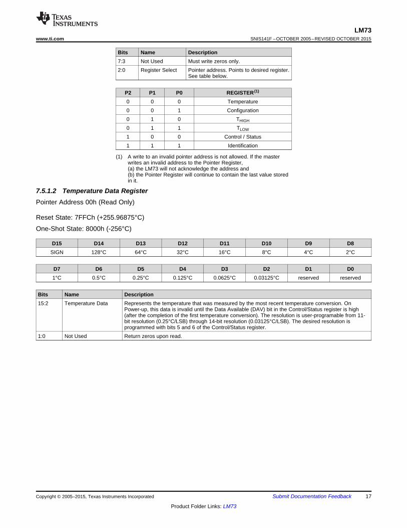
12 Mechanical, Packaging, and Orderable InformationThe following pages include mechanical, packaging, and orderable information. This information is the mostcurrent data available for the designated devices. This data is subject to change without notice and revision ofthis document. For browser-based versions of this data sheet, refer to the left-hand navigation.
Copyright © 2005–2015, Texas Instruments Incorporated Submit Documentation Feedback 23
Product Folder Links: LM73

PACKAGE OPTION ADDENDUM
www.ti.com 28-Feb-2017
Addendum-Page 1
PACKAGING INFORMATION
Orderable Device Status(1)
Package Type PackageDrawing
Pins PackageQty
Eco Plan(2)
Lead/Ball Finish(6)
MSL Peak Temp(3)
Op Temp (°C) Device Marking(4/5)
Samples
LM73CIMK-0/NOPB ACTIVE SOT-23-THIN DDC 6 1000 Green (RoHS& no Sb/Br)
CU NIPDAU Level-1-260C-UNLIM -40 to 150 T730
LM73CIMK-1/NOPB ACTIVE SOT-23-THIN DDC 6 1000 Green (RoHS& no Sb/Br)
CU NIPDAU Level-1-260C-UNLIM -40 to 150 T731
LM73CIMKX-0/NOPB ACTIVE SOT-23-THIN DDC 6 3000 Green (RoHS& no Sb/Br)
CU NIPDAU Level-1-260C-UNLIM -40 to 150 T730
LM73CIMKX-1/NOPB ACTIVE SOT-23-THIN DDC 6 3000 Green (RoHS& no Sb/Br)
CU NIPDAU Level-1-260C-UNLIM -40 to 150 T731
(1) The marketing status values are defined as follows:ACTIVE: Product device recommended for new designs.LIFEBUY: TI has announced that the device will be discontinued, and a lifetime-buy period is in effect.NRND: Not recommended for new designs. Device is in production to support existing customers, but TI does not recommend using this part in a new design.PREVIEW: Device has been announced but is not in production. Samples may or may not be available.OBSOLETE: TI has discontinued the production of the device.
(2) Eco Plan - The planned eco-friendly classification: Pb-Free (RoHS), Pb-Free (RoHS Exempt), or Green (RoHS & no Sb/Br) - please check http://www.ti.com/productcontent for the latest availabilityinformation and additional product content details.TBD: The Pb-Free/Green conversion plan has not been defined.Pb-Free (RoHS): TI's terms "Lead-Free" or "Pb-Free" mean semiconductor products that are compatible with the current RoHS requirements for all 6 substances, including the requirement thatlead not exceed 0.1% by weight in homogeneous materials. Where designed to be soldered at high temperatures, TI Pb-Free products are suitable for use in specified lead-free processes.Pb-Free (RoHS Exempt): This component has a RoHS exemption for either 1) lead-based flip-chip solder bumps used between the die and package, or 2) lead-based die adhesive used betweenthe die and leadframe. The component is otherwise considered Pb-Free (RoHS compatible) as defined above.Green (RoHS & no Sb/Br): TI defines "Green" to mean Pb-Free (RoHS compatible), and free of Bromine (Br) and Antimony (Sb) based flame retardants (Br or Sb do not exceed 0.1% by weightin homogeneous material)
(3) MSL, Peak Temp. - The Moisture Sensitivity Level rating according to the JEDEC industry standard classifications, and peak solder temperature.
(4) There may be additional marking, which relates to the logo, the lot trace code information, or the environmental category on the device.
(5) Multiple Device Markings will be inside parentheses. Only one Device Marking contained in parentheses and separated by a "~" will appear on a device. If a line is indented then it is a continuationof the previous line and the two combined represent the entire Device Marking for that device.
(6) Lead/Ball Finish - Orderable Devices may have multiple material finish options. Finish options are separated by a vertical ruled line. Lead/Ball Finish values may wrap to two lines if the finishvalue exceeds the maximum column width.

PACKAGE OPTION ADDENDUM
www.ti.com 28-Feb-2017
Addendum-Page 2
Important Information and Disclaimer:The information provided on this page represents TI's knowledge and belief as of the date that it is provided. TI bases its knowledge and belief on informationprovided by third parties, and makes no representation or warranty as to the accuracy of such information. Efforts are underway to better integrate information from third parties. TI has taken andcontinues to take reasonable steps to provide representative and accurate information but may not have conducted destructive testing or chemical analysis on incoming materials and chemicals.TI and TI suppliers consider certain information to be proprietary, and thus CAS numbers and other limited information may not be available for release.
In no event shall TI's liability arising out of such information exceed the total purchase price of the TI part(s) at issue in this document sold by TI to Customer on an annual basis.
OTHER QUALIFIED VERSIONS OF LM73 :
• Automotive: LM73-Q1
NOTE: Qualified Version Definitions:
• Automotive - Q100 devices qualified for high-reliability automotive applications targeting zero defects

TAPE AND REEL INFORMATION
*All dimensions are nominal
Device PackageType
PackageDrawing
Pins SPQ ReelDiameter
(mm)
ReelWidth
W1 (mm)
A0(mm)
B0(mm)
K0(mm)
P1(mm)
W(mm)
Pin1Quadrant
LM73CIMK-0/NOPB SOT-23-THIN
DDC 6 1000 178.0 8.4 3.2 3.2 1.4 4.0 8.0 Q3
LM73CIMK-1/NOPB SOT-23-THIN
DDC 6 1000 178.0 8.4 3.2 3.2 1.4 4.0 8.0 Q3
LM73CIMKX-0/NOPB SOT-23-THIN
DDC 6 3000 178.0 8.4 3.2 3.2 1.4 4.0 8.0 Q3
LM73CIMKX-1/NOPB SOT-23-THIN
DDC 6 3000 178.0 8.4 3.2 3.2 1.4 4.0 8.0 Q3
PACKAGE MATERIALS INFORMATION
www.ti.com 3-Mar-2017
Pack Materials-Page 1

*All dimensions are nominal
Device Package Type Package Drawing Pins SPQ Length (mm) Width (mm) Height (mm)
LM73CIMK-0/NOPB SOT-23-THIN DDC 6 1000 210.0 185.0 35.0
LM73CIMK-1/NOPB SOT-23-THIN DDC 6 1000 210.0 185.0 35.0
LM73CIMKX-0/NOPB SOT-23-THIN DDC 6 3000 210.0 185.0 35.0
LM73CIMKX-1/NOPB SOT-23-THIN DDC 6 3000 210.0 185.0 35.0
PACKAGE MATERIALS INFORMATION
www.ti.com 3-Mar-2017
Pack Materials-Page 2


IMPORTANT NOTICE
Texas Instruments Incorporated (TI) reserves the right to make corrections, enhancements, improvements and other changes to itssemiconductor products and services per JESD46, latest issue, and to discontinue any product or service per JESD48, latest issue. Buyersshould obtain the latest relevant information before placing orders and should verify that such information is current and complete.TI’s published terms of sale for semiconductor products (http://www.ti.com/sc/docs/stdterms.htm) apply to the sale of packaged integratedcircuit products that TI has qualified and released to market. Additional terms may apply to the use or sale of other types of TI products andservices.Reproduction of significant portions of TI information in TI data sheets is permissible only if reproduction is without alteration and isaccompanied by all associated warranties, conditions, limitations, and notices. TI is not responsible or liable for such reproduceddocumentation. Information of third parties may be subject to additional restrictions. Resale of TI products or services with statementsdifferent from or beyond the parameters stated by TI for that product or service voids all express and any implied warranties for theassociated TI product or service and is an unfair and deceptive business practice. TI is not responsible or liable for any such statements.Buyers and others who are developing systems that incorporate TI products (collectively, “Designers”) understand and agree that Designersremain responsible for using their independent analysis, evaluation and judgment in designing their applications and that Designers havefull and exclusive responsibility to assure the safety of Designers' applications and compliance of their applications (and of all TI productsused in or for Designers’ applications) with all applicable regulations, laws and other applicable requirements. Designer represents that, withrespect to their applications, Designer has all the necessary expertise to create and implement safeguards that (1) anticipate dangerousconsequences of failures, (2) monitor failures and their consequences, and (3) lessen the likelihood of failures that might cause harm andtake appropriate actions. Designer agrees that prior to using or distributing any applications that include TI products, Designer willthoroughly test such applications and the functionality of such TI products as used in such applications.TI’s provision of technical, application or other design advice, quality characterization, reliability data or other services or information,including, but not limited to, reference designs and materials relating to evaluation modules, (collectively, “TI Resources”) are intended toassist designers who are developing applications that incorporate TI products; by downloading, accessing or using TI Resources in anyway, Designer (individually or, if Designer is acting on behalf of a company, Designer’s company) agrees to use any particular TI Resourcesolely for this purpose and subject to the terms of this Notice.TI’s provision of TI Resources does not expand or otherwise alter TI’s applicable published warranties or warranty disclaimers for TIproducts, and no additional obligations or liabilities arise from TI providing such TI Resources. TI reserves the right to make corrections,enhancements, improvements and other changes to its TI Resources. TI has not conducted any testing other than that specificallydescribed in the published documentation for a particular TI Resource.Designer is authorized to use, copy and modify any individual TI Resource only in connection with the development of applications thatinclude the TI product(s) identified in such TI Resource. NO OTHER LICENSE, EXPRESS OR IMPLIED, BY ESTOPPEL OR OTHERWISETO ANY OTHER TI INTELLECTUAL PROPERTY RIGHT, AND NO LICENSE TO ANY TECHNOLOGY OR INTELLECTUAL PROPERTYRIGHT OF TI OR ANY THIRD PARTY IS GRANTED HEREIN, including but not limited to any patent right, copyright, mask work right, orother intellectual property right relating to any combination, machine, or process in which TI products or services are used. Informationregarding or referencing third-party products or services does not constitute a license to use such products or services, or a warranty orendorsement thereof. Use of TI Resources may require a license from a third party under the patents or other intellectual property of thethird party, or a license from TI under the patents or other intellectual property of TI.TI RESOURCES ARE PROVIDED “AS IS” AND WITH ALL FAULTS. TI DISCLAIMS ALL OTHER WARRANTIES ORREPRESENTATIONS, EXPRESS OR IMPLIED, REGARDING RESOURCES OR USE THEREOF, INCLUDING BUT NOT LIMITED TOACCURACY OR COMPLETENESS, TITLE, ANY EPIDEMIC FAILURE WARRANTY AND ANY IMPLIED WARRANTIES OFMERCHANTABILITY, FITNESS FOR A PARTICULAR PURPOSE, AND NON-INFRINGEMENT OF ANY THIRD PARTY INTELLECTUALPROPERTY RIGHTS. TI SHALL NOT BE LIABLE FOR AND SHALL NOT DEFEND OR INDEMNIFY DESIGNER AGAINST ANY CLAIM,INCLUDING BUT NOT LIMITED TO ANY INFRINGEMENT CLAIM THAT RELATES TO OR IS BASED ON ANY COMBINATION OFPRODUCTS EVEN IF DESCRIBED IN TI RESOURCES OR OTHERWISE. IN NO EVENT SHALL TI BE LIABLE FOR ANY ACTUAL,DIRECT, SPECIAL, COLLATERAL, INDIRECT, PUNITIVE, INCIDENTAL, CONSEQUENTIAL OR EXEMPLARY DAMAGES INCONNECTION WITH OR ARISING OUT OF TI RESOURCES OR USE THEREOF, AND REGARDLESS OF WHETHER TI HAS BEENADVISED OF THE POSSIBILITY OF SUCH DAMAGES.Unless TI has explicitly designated an individual product as meeting the requirements of a particular industry standard (e.g., ISO/TS 16949and ISO 26262), TI is not responsible for any failure to meet such industry standard requirements.Where TI specifically promotes products as facilitating functional safety or as compliant with industry functional safety standards, suchproducts are intended to help enable customers to design and create their own applications that meet applicable functional safety standardsand requirements. Using products in an application does not by itself establish any safety features in the application. Designers mustensure compliance with safety-related requirements and standards applicable to their applications. Designer may not use any TI products inlife-critical medical equipment unless authorized officers of the parties have executed a special contract specifically governing such use.Life-critical medical equipment is medical equipment where failure of such equipment would cause serious bodily injury or death (e.g., lifesupport, pacemakers, defibrillators, heart pumps, neurostimulators, and implantables). Such equipment includes, without limitation, allmedical devices identified by the U.S. Food and Drug Administration as Class III devices and equivalent classifications outside the U.S.TI may expressly designate certain products as completing a particular qualification (e.g., Q100, Military Grade, or Enhanced Product).Designers agree that it has the necessary expertise to select the product with the appropriate qualification designation for their applicationsand that proper product selection is at Designers’ own risk. Designers are solely responsible for compliance with all legal and regulatoryrequirements in connection with such selection.Designer will fully indemnify TI and its representatives against any damages, costs, losses, and/or liabilities arising out of Designer’s non-compliance with the terms and provisions of this Notice.
Mailing Address: Texas Instruments, Post Office Box 655303, Dallas, Texas 75265Copyright © 2017, Texas Instruments Incorporated