LM35 高精度摄氏温度传感器 datasheet (Rev. H)
37
LM35 +V S R1 V OUT tV S LM35 +V S (4 V to 20 V) OUTPUT 0 mV + 10.0 mV/°C Product Folder Order Now Technical Documents Tools & Software Support & Community An IMPORTANT NOTICE at the end of this data sheet addresses availability, warranty, changes, use in safety-critical applications, intellectual property matters and other important disclaimers. PRODUCTION DATA. English Data Sheet: SNIS159 LM35 ZHCSHC4H – AUGUST 1999 – REVISED DECEMBER 2017 LM35 高精度摄氏温度传感器 1 1 特性 1• 直接以摄氏温度(摄氏度)进行校准 • 线性 +10mV/°C 比例因子 • 0.5°C 的确保精度(25°C 时) • 额定温度范围为 −55°C 至 150°C • 适用于远程 应用 • 晶圆级修整实现低成本 • 工作电压范围 4V 至 30V • 电流漏极小于 60μA • 低自发热,处于静止的空气中时为 0.08°C • 非线性典型值仅 ±¼°C • 低阻抗输出,1mA 负载时为 0.1Ω 2 应用 • 电源 • 电池管理 • HVAC • 电器 3 说明 LM35 系列产品是高精度集成电路温度器件,其输出电 压与摄氏温度成线性正比关系。相比于以开尔文温度校 准的线性温度传感器,LM35 器件的优势在于使用者无 需在输出电压中减去一个较大的恒定电压值即可便捷地 实现摄氏度调节。LM35 器件无需进行任何外部校准或 修整,可在室温下提供 ±¼°C 的典型精度,而在 −55°C 至 +150°C 的完整温度范围内提供 ±¾°C 的精 度。晶圆级的修正和校准可确保更低的成本。LM35 器 件具有低输出阻抗、线性输出和高精度内在校准功能, 这些特性使得连接读取或控制电路变得尤为简单。此器 件可使用单电源或正负电源供电。因为 LM35 器件仅 需从电源中消耗 60μA 的电流,所以处于静止的空气中 时具有不到 0.1°C 的极低自发热。LM35 器件额定工作 温度范围为 −55°C 至 150°C,LM35C 器件额定工作 温度范围 −40°C 至 110°C(−10° 时精度更高)。 LM35 系列器件采用密封 TO 晶体管封装,LM35C、 LM35CA 和 LM35D 器件采用塑料 TO-92 晶体管封 装。LM35D 器件采用 8 引线表面贴装小外形封装和塑 料 TO-220 封装。 器件信息 (1) 器件型号 封装 封装尺寸(标称值) LM35 TO-CAN (3) 4.699mm × 4.699mm TO-92 (3) 4.30mm × 4.30mm SOIC (8) 4.90mm x 3.91mm TO-220 (3) 14.986mm × 10.16mm (1) 如需了解所有可用封装,请参阅数据表末尾的可订购产品附 录。 基本摄氏温度传感器 (2°C 至 150°C) 全范围摄氏温度传感器 选择 R 1 = –V S /50μA 150°C 时,V OUT = 1500mV 25°C 时,V OUT = 250mV –55°C 时,V OUT = –550mV
Transcript of LM35 高精度摄氏温度传感器 datasheet (Rev. H)

LM35
+VS
R1
VOUT
tVS
LM35
+VS
(4 V to 20 V)
OUTPUT
0 mV + 10.0 mV/°C
Product
Folder
Order
Now
Technical
Documents
Tools &
Software
Support &Community
An IMPORTANT NOTICE at the end of this data sheet addresses availability, warranty, changes, use in safety-critical applications,intellectual property matters and other important disclaimers. PRODUCTION DATA.
English Data Sheet: SNIS159
LM35ZHCSHC4H –AUGUST 1999–REVISED DECEMBER 2017
LM35 高高精精度度摄摄氏氏温温度度传传感感器器
1
1 特特性性
1• 直接以摄氏温度(摄氏度)进行校准
• 线性 +10mV/°C 比例因子
• 0.5°C 的确保精度(25°C 时)
• 额定温度范围为 −55°C 至 150°C• 适用于远程 应用
• 晶圆级修整实现低成本
• 工作电压范围 4V 至 30V• 电流漏极小于 60μA• 低自发热,处于静止的空气中时为 0.08°C• 非线性典型值仅 ±¼°C• 低阻抗输出,1mA 负载时为 0.1Ω
2 应应用用
• 电源
• 电池管理
• HVAC• 电器
3 说说明明
LM35 系列产品是高精度集成电路温度器件,其输出电
压与摄氏温度成线性正比关系。相比于以开尔文温度校
准的线性温度传感器,LM35 器件的优势在于使用者无
需在输出电压中减去一个较大的恒定电压值即可便捷地
实现摄氏度调节。LM35 器件无需进行任何外部校准或
修整,可在室温下提供 ±¼°C 的典型精度,而在
−55°C 至 +150°C 的完整温度范围内提供 ±¾°C 的精
度。晶圆级的修正和校准可确保更低的成本。LM35 器
件具有低输出阻抗、线性输出和高精度内在校准功能,
这些特性使得连接读取或控制电路变得尤为简单。此器
件可使用单电源或正负电源供电。因为 LM35 器件仅
需从电源中消耗 60μA 的电流,所以处于静止的空气中
时具有不到 0.1°C 的极低自发热。LM35 器件额定工作
温度范围为 −55°C 至 150°C,LM35C 器件额定工作
温度范围 −40°C 至 110°C(−10° 时精度更高)。
LM35 系列器件采用密封 TO 晶体管封装,LM35C、
LM35CA 和 LM35D 器件采用塑料 TO-92 晶体管封
装。LM35D 器件采用 8 引线表面贴装小外形封装和塑
料 TO-220 封装。
器器件件信信息息(1)
器器件件型型号号 封封装装 封封装装尺尺寸寸((标标称称值值))
LM35
TO-CAN (3) 4.699mm × 4.699mmTO-92 (3) 4.30mm × 4.30mmSOIC (8) 4.90mm x 3.91mmTO-220 (3) 14.986mm × 10.16mm
(1) 如需了解所有可用封装,请参阅数据表末尾的可订购产品附录。
基基本本摄摄氏氏温温度度传传感感器器((2°C 至至 150°C))
全全范范围围摄摄氏氏温温度度传传感感器器
选择 R1 = –VS/50µA150°C 时,VOUT = 1500mV25°C 时,VOUT = 250mV–55°C 时,VOUT = –550mV

2
LM35ZHCSHC4H –AUGUST 1999–REVISED DECEMBER 2017 www.ti.com.cn
Copyright © 1999–2017, Texas Instruments Incorporated
目目录录
1 特特性性.......................................................................... 12 应应用用.......................................................................... 13 说说明明.......................................................................... 14 修修订订历历史史记记录录 ........................................................... 25 Pin Configuration and Functions ......................... 36 Specifications......................................................... 4
6.1 Absolute Maximum Ratings ...................................... 46.2 ESD Ratings.............................................................. 46.3 Recommended Operating Conditions....................... 46.4 Thermal Information .................................................. 46.5 Electrical Characteristics: LM35A, LM35CA Limits... 56.6 Electrical Characteristics: LM35A, LM35CA ............. 66.7 Electrical Characteristics: LM35, LM35C, LM35D
Limits.......................................................................... 86.8 Electrical Characteristics: LM35, LM35C, LM35D ... 96.9 Typical Characteristics ............................................ 11
7 Detailed Description ............................................ 137.1 Overview ................................................................. 13
7.2 Functional Block Diagram ....................................... 137.3 Feature Description................................................. 137.4 Device Functional Modes........................................ 13
8 Application and Implementation ........................ 148.1 Application Information............................................ 148.2 Typical Application .................................................. 158.3 System Examples ................................................... 16
9 Power Supply Recommendations ...................... 1910 Layout................................................................... 19
10.1 Layout Guidelines ................................................. 1910.2 Layout Example .................................................... 20
11 器器件件和和文文档档支支持持 ..................................................... 2111.1 接收文档更新通知 ................................................. 2111.2 社区资源 ................................................................ 2111.3 商标 ....................................................................... 2111.4 静电放电警告......................................................... 2111.5 Glossary ................................................................ 21
12 机机械械、、封封装装和和可可订订购购信信息息....................................... 21
4 修修订订历历史史记记录录
Changes from Revision G (August 2016) to Revision H Page
• Changed NDV Package (TO-CAN) pinout from bottom view back to top view; added textnote to pinout............................. 3• Added pin numbers to the TO-CAN (TO46) pinout ................................................................................................................ 3
Changes from Revision F (January 2016) to Revision G Page
• Equation 1, changed From: 10 mV/°F To: 10mv/°C ............................................................................................................ 13• Power Supply Recommendations, changed From: "4-V to 5.5-V power supply" To: "4-V to 30-V power supply: .............. 19
Changes from Revision E (January 2015) to Revision F Page
• Changed NDV Package (TO-CAN) pinout from Top View to Bottom View ........................................................................... 3
Changes from Revision D (October 2013) to Revision E Page
• 已添加 引脚配置和功能 部分、ESD 额定值表、特性 说明 部分、器件功能模式、应用和实施 部分、电源相关建议 部分、布局 部分、器件和文档支持 部分以及机械、封装和可订购信息 部分 ............................................................................. 1
Changes from Revision C (July 2013) to Revision D Page
• 已更改 将 W更改为 Ω 添加了.................................................................................................................................................. 1• Changed W to Ω in Abs Max tablenote. ................................................................................................................................ 4

+VS VOUTGND
LM35DT
1 2 3
+VSVOUT
GND
N.C.
N.C.
N.C.
N.C.
N.C.
12
3
4
87
6
5
+VS VOUT GND
321
(1) +VS
(2) VOUT
(3) GND
3
LM35www.ti.com.cn ZHCSHC4H –AUGUST 1999–REVISED DECEMBER 2017
Copyright © 1999–2017, Texas Instruments Incorporated
5 Pin Configuration and Functions
NDV Package3-Pin TO-CAN
(Top View)
Case is connected to negative pin (GND)Refer the second NDV0003H page forreference
D Package8-PIN SOIC(Top View)
N.C. = No connection
LP Package3-Pin TO-92
(Bottom View)
NEB Package3-Pin TO-220(Top View)
Tab is connected to the negative pin(GND).NOTE: The LM35DT pinout is different thanthe discontinued LM35DP
Pin FunctionsPIN
TYPE DESCRIPTIONNAME TO46 TO92 TO220 SO8VOUT 2 2 3 1 O Temperature Sensor Analog Output
N.C.— — — 2
— No Connection— — — 3
GND 3 3 2 4 GROUND Device ground pin, connect to power supply negativeterminal
N.C.— — — 5
— No Connection— — — 6— — — 7
+VS 1 1 1 8 POWER Positive power supply pin

4
LM35ZHCSHC4H –AUGUST 1999–REVISED DECEMBER 2017 www.ti.com.cn
Copyright © 1999–2017, Texas Instruments Incorporated
(1) If Military/Aerospace specified devices are required, please contact the Texas Instruments Sales Office/ Distributors for availability andspecifications.
(2) Absolute Maximum Ratings indicate limits beyond which damage to the device may occur. DC and AC electrical specifications do notapply when operating the device beyond its rated operating conditions.
6 Specifications
6.1 Absolute Maximum Ratingsover operating free-air temperature range (unless otherwise noted) (1) (2)
MIN MAX UNITSupply voltage –0.2 35 VOutput voltage –1 6 VOutput current 10 mAMaximum Junction Temperature, TJmax 150 °C
Storage Temperature, TstgTO-CAN, TO-92 Package –60 150
°CTO-220, SOIC Package –65 150
(1) JEDEC document JEP155 states that 500-V HBM allows safe manufacturing with a standard ESD control process.
6.2 ESD RatingsVALUE UNIT
V(ESD) Electrostatic discharge Human-body model (HBM), per ANSI/ESDA/JEDEC JS-001 (1) ±2500 V
6.3 Recommended Operating Conditionsover operating free-air temperature range (unless otherwise noted)
MIN MAX UNIT
Specified operating temperature: TMIN toTMAX
LM35, LM35A –55 150°CLM35C, LM35CA –40 110
LM35D 0 100Supply Voltage (+VS) 4 30 V
(1) For more information about traditional and new thermal metrics, see the IC Package Thermal Metrics application report, SPRA953.(2) For additional thermal resistance information, see Typical Application.
6.4 Thermal Information
THERMAL METRIC (1) (2)LM35
UNITNDV LP D NEB3 PINS 8 PINS 3 PINS
RθJA Junction-to-ambient thermal resistance 400 180 220 90°C/W
RθJC(top) Junction-to-case (top) thermal resistance 24 — — —

5
LM35www.ti.com.cn ZHCSHC4H –AUGUST 1999–REVISED DECEMBER 2017
Copyright © 1999–2017, Texas Instruments Incorporated
(1) Tested Limits are ensured and 100% tested in production.(2) Design Limits are ensured (but not 100% production tested) over the indicated temperature and supply voltage ranges. These limits are
not used to calculate outgoing quality levels.(3) Accuracy is defined as the error between the output voltage and 10 mv/°C times the case temperature of the device, at specified
conditions of voltage, current, and temperature (expressed in °C).(4) Non-linearity is defined as the deviation of the output-voltage-versus-temperature curve from the best-fit straight line, over the rated
temperature range of the device.(5) Regulation is measured at constant junction temperature, using pulse testing with a low duty cycle. Changes in output due to heating
effects can be computed by multiplying the internal dissipation by the thermal resistance.(6) Quiescent current is defined in the circuit of Figure 14.
6.5 Electrical Characteristics: LM35A, LM35CA LimitsUnless otherwise noted, these specifications apply: −55°C ≤ TJ ≤ 150°C for the LM35 and LM35A; −40°C ≤ TJ ≤ 110°C for theLM35C and LM35CA; and 0°C ≤ TJ ≤ 100°C for the LM35D. VS = 5 Vdc and ILOAD = 50 μA, in the circuit of Full-RangeCentigrade Temperature Sensor. These specifications also apply from 2°C to TMAX in the circuit of Figure 14.
PARAMETER TEST CONDITIONSLM35A LM35CA
UNITTYP TESTEDLIMIT (1)
DESIGNLIMIT (2)
TYP TESTEDLIMIT (1)
DESIGNLIMIT (2)
Accuracy (3)
TA = 25°C ±0.2 ±0.5 ±0.2 ±0.5
°CTA = –10°C ±0.3 ±0.3 ±1TA = TMAX ±0.4 ±1 ±0.4 ±1TA = TMIN ±0.4 ±1 ±0.4 ±1.5
Nonlinearity (4) TMIN ≤ TA ≤ TMAX,–40°C ≤ TJ ≤ 125°C ±0.18 ±0.35 ±0.15 ±0.3 °C
Sensor gain(average slope)
TMIN ≤ TA ≤ TMAX 10 9.9 10 9.9mV/°C
–40°C ≤ TJ ≤ 125°C 10 10.1 10 10.1
Load regulation (5)
0 ≤ IL ≤ 1 mA
TA = 25°C ±0.4 ±1 ±0.4 ±1mV/mATMIN ≤ TA ≤ TMAX,
–40°C ≤ TJ ≤ 125°C ±0.5 ±3 ±0.5 ±3
Line regulation (5)TA = 25°C ±0.01 ±0.05 ±0.01 ±0.05
mV/V4 V ≤ VS ≤ 30 V,–40°C ≤ TJ ≤ 125°C ±0.02 ±0.1 ±0.02 ±0.1
Quiescent current (6)
VS = 5 V, 25°C 56 67 56 67
µAVS = 5 V, –40°C ≤ TJ ≤ 125°C 105 131 91 114VS = 30 V, 25°C 56.2 68 56.2 68VS = 30 V, –40°C ≤ TJ ≤ 125°C 105.5 133 91.5 116
Change of quiescentcurrent (5)
4 V ≤ VS ≤ 30 V, 25°C 0.2 1 0.2 1µA4 V ≤ VS ≤ 30 V,
–40°C ≤ TJ ≤ 125°C 0.5 2 0.5 2
Temperaturecoefficient ofquiescent current
–40°C ≤ TJ ≤ 125°C 0.39 0.5 0.39 0.5 µA/°C
Minimum temperaturefor rate accuracy In circuit of Figure 14, IL = 0 1.5 2 1.5 2 °C
Long term stability TJ = TMAX, for 1000 hours ±0.08 ±0.08 °C

6
LM35ZHCSHC4H –AUGUST 1999–REVISED DECEMBER 2017 www.ti.com.cn
Copyright © 1999–2017, Texas Instruments Incorporated
(1) Accuracy is defined as the error between the output voltage and 10 mv/°C times the case temperature of the device, at specifiedconditions of voltage, current, and temperature (expressed in °C).
(2) Tested Limits are ensured and 100% tested in production.(3) Design Limits are ensured (but not 100% production tested) over the indicated temperature and supply voltage ranges. These limits are
not used to calculate outgoing quality levels.(4) Non-linearity is defined as the deviation of the output-voltage-versus-temperature curve from the best-fit straight line, over the rated
temperature range of the device.(5) Regulation is measured at constant junction temperature, using pulse testing with a low duty cycle. Changes in output due to heating
effects can be computed by multiplying the internal dissipation by the thermal resistance.
6.6 Electrical Characteristics: LM35A, LM35CAUnless otherwise noted, these specifications apply: −55°C ≤ TJ ≤ 150°C for the LM35 and LM35A; −40°C ≤ TJ ≤ 110°C for theLM35C and LM35CA; and 0°C ≤ TJ ≤ 100°C for the LM35D. VS = 5 Vdc and ILOAD = 50 μA, in the circuit of Full-RangeCentigrade Temperature Sensor. These specifications also apply from 2°C to TMAX in the circuit of Figure 14.
PARAMETER TEST CONDITIONSLM35A LM35CA
UNITMIN TYP MAX TYP TYP MAX
Accuracy (1)
TA = 25°C±0.2 ±0.2
°C
Tested Limit (2) ±0.5 ±0.5Design Limit (3)
TA = –10°C±0.3 ±0.3
Tested Limit (2)
Design Limit (3) ±1
TA = TMAX
±0.4 ±0.4Tested Limit (2) ±1 ±1Design Limit (3)
TA = TMIN
±0.4 ±0.4Tested Limit (2) ±1Design Limit (3) ±1.5
Nonlinearity (4) TMIN ≤ TA ≤ TMAX,–40°C ≤ TJ ≤ 125°C
±0.18 ±0.15°CTested Limit (2)
Design Limit (3) ±0.35 ±0.3
Sensor gain(average slope)
TMIN ≤ TA ≤ TMAX
10 10
mV/°C
Tested Limit (2) 9.9Design Limit (3) 9.9
–40°C ≤ TJ ≤ 125°C10 10
Tested Limit (2) 10.1Design Limit (3) 10.1
Load regulation (5)
0 ≤ IL ≤ 1 mA
TA = 25°C±0.4 ±0.4
mV/mA
Tested Limit (2) ±1 ±1Design Limit (3)
TMIN ≤ TA ≤ TMAX,–40°C ≤ TJ ≤ 125°C
±0.5 ±0.5Tested Limit (2)
Design Limit (3) ±3 ±3
Line regulation (5)
TA = 25°C±0.01 ±0.01
mV/V
Tested Limit (2) ±0.05 ±0.05Design Limit (3)
4 V ≤ VS ≤ 30 V,–40°C ≤ TJ ≤ 125°C
±0.02 ±0.02Tested Limit (2)
Design Limit (3) ±0.1 ±0.1

7
LM35www.ti.com.cn ZHCSHC4H –AUGUST 1999–REVISED DECEMBER 2017
Copyright © 1999–2017, Texas Instruments Incorporated
Electrical Characteristics: LM35A, LM35CA (continued)Unless otherwise noted, these specifications apply: −55°C ≤ TJ ≤ 150°C for the LM35 and LM35A; −40°C ≤ TJ ≤ 110°C for theLM35C and LM35CA; and 0°C ≤ TJ ≤ 100°C for the LM35D. VS = 5 Vdc and ILOAD = 50 μA, in the circuit of Full-RangeCentigrade Temperature Sensor. These specifications also apply from 2°C to TMAX in the circuit of Figure 14.
PARAMETER TEST CONDITIONSLM35A LM35CA
UNITMIN TYP MAX TYP TYP MAX
(6) Quiescent current is defined in the circuit of Figure 14.
Quiescentcurrent (6)
VS = 5 V, 25°C56 56
µA
Tested Limit (2) 67 67Design Limit (3)
VS = 5 V,–40°C ≤ TJ ≤ 125°C
105 91Tested Limit (2)
Design Limit (3) 131 114
VS = 30 V, 25°C56.2 56.2
Tested Limit (2) 68 68Design Limit (3)
VS = 30 V,–40°C ≤ TJ ≤ 125°C
105.5 91.5Tested Limit (2)
Design Limit (3) 133 116
Change ofquiescentcurrent (5)
4 V ≤ VS ≤ 30 V, 25°C0.2 0.2
µA
Tested Limit (2) 1 1Design Limit (3)
4 V ≤ VS ≤ 30 V,–40°C ≤ TJ ≤ 125°C
0.5 0.5Tested Limit (2)
Design Limit (3) 2 2
Temperaturecoefficient ofquiescent current
–40°C ≤ TJ ≤ 125°C0.39 0.39
µA/°CTested Limit (2)
Design Limit (3) 0.5 0.5
Minimumtemperature forrate accuracy
In circuit of Figure 14, IL =0
1.5 1.5°CTested Limit (2)
Design Limit (3) 2 2Long termstability TJ = TMAX, for 1000 hours ±0.08 ±0.08 °C

8
LM35ZHCSHC4H –AUGUST 1999–REVISED DECEMBER 2017 www.ti.com.cn
Copyright © 1999–2017, Texas Instruments Incorporated
(1) Tested Limits are ensured and 100% tested in production.(2) Design Limits are ensured (but not 100% production tested) over the indicated temperature and supply voltage ranges. These limits are
not used to calculate outgoing quality levels.(3) Accuracy is defined as the error between the output voltage and 10 mv/°C times the case temperature of the device, at specified
conditions of voltage, current, and temperature (expressed in °C).(4) Non-linearity is defined as the deviation of the output-voltage-versus-temperature curve from the best-fit straight line, over the rated
temperature range of the device.(5) Regulation is measured at constant junction temperature, using pulse testing with a low duty cycle. Changes in output due to heating
effects can be computed by multiplying the internal dissipation by the thermal resistance.(6) Quiescent current is defined in the circuit of Figure 14.
6.7 Electrical Characteristics: LM35, LM35C, LM35D LimitsUnless otherwise noted, these specifications apply: −55°C ≤ TJ ≤ 150°C for the LM35 and LM35A; −40°C ≤ TJ ≤ 110°C for theLM35C and LM35CA; and 0°C ≤ TJ ≤ 100°C for the LM35D. VS = 5 Vdc and ILOAD = 50 μA, in the circuit of Full-RangeCentigrade Temperature Sensor. These specifications also apply from 2°C to TMAX in the circuit of Figure 14.
PARAMETER TEST CONDITIONSLM35 LM35C, LM35D
UNITTYP TESTEDLIMIT (1)
DESIGNLIMIT (2)
TYP TESTEDLIMIT (1)
DESIGNLIMIT (2)
Accuracy, LM35,LM35C (3)
TA = 25°C ±0.4 ±1 ±0.4 ±1
°CTA = –10°C ±0.5 ±0.5 ±1.5TA = TMAX ±0.8 ±1.5 ±0.8 ±1.5TA = TMIN ±0.8 ±1.5 ±0.8 ±2
Accuracy, LM35D (3)
TA = 25°C ±0.6 ±1.5°CTA = TMAX ±0.9 ±2
TA = TMIN ±0.9 ±2
Nonlinearity (4) TMIN ≤ TA ≤ TMAX,–40°C ≤ TJ ≤ 125°C ±0.3 ±0.5 ±0.2 ±0.5 °C
Sensor gain(average slope)
TMIN ≤ TA ≤ TMAX,–40°C ≤ TJ ≤ 125°C 10 9.8 10 9.8
mV/°C10 10.2 10 10.2
Load regulation (5)
0 ≤ IL ≤ 1 mA
TA = 25°C ±0.4 ±2 ±0.4 ±2mV/mATMIN ≤ TA ≤ TMAX,
–40°C ≤ TJ ≤ 125°C ±0.5 ±5 ±0.5 ±5
Line regulation (5)TA = 25°C ±0.01 ±0.1 ±0.01 ±0.1
mV/V4 V ≤ VS ≤ 30 V,–40°C ≤ TJ ≤ 125°C ±0.02 ±0.2 ±0.02 ±0.2
Quiescent current (6)
VS = 5 V, 25°C 56 80 56 80
µAVS = 5 V, –40°C ≤ TJ ≤ 125°C 105 158 91 138VS = 30 V, 25°C 56.2 82 56.2 82VS = 30 V, –40°C ≤ TJ ≤ 125°C 105.5 161 91.5 141
Change of quiescentcurrent (5)
4 V ≤ VS ≤ 30 V, 25°C 0.2 2 0.2 2µA4 V ≤ VS ≤ 30 V,
–40°C ≤ TJ ≤ 125°C 0.5 3 0.5 3
Temperaturecoefficient ofquiescent current
–40°C ≤ TJ ≤ 125°C 0.39 0.7 0.39 0.7 µA/°C
Minimum temperaturefor rate accuracy In circuit of Figure 14, IL = 0 1.5 2 1.5 2 °C
Long term stability TJ = TMAX, for 1000 hours ±0.08 ±0.08 °C

9
LM35www.ti.com.cn ZHCSHC4H –AUGUST 1999–REVISED DECEMBER 2017
Copyright © 1999–2017, Texas Instruments Incorporated
(1) Accuracy is defined as the error between the output voltage and 10 mv/°C times the case temperature of the device, at specifiedconditions of voltage, current, and temperature (expressed in °C).
(2) Tested Limits are ensured and 100% tested in production.(3) Design Limits are ensured (but not 100% production tested) over the indicated temperature and supply voltage ranges. These limits are
not used to calculate outgoing quality levels.(4) Non-linearity is defined as the deviation of the output-voltage-versus-temperature curve from the best-fit straight line, over the rated
temperature range of the device.(5) Regulation is measured at constant junction temperature, using pulse testing with a low duty cycle. Changes in output due to heating
effects can be computed by multiplying the internal dissipation by the thermal resistance.
6.8 Electrical Characteristics: LM35, LM35C, LM35DUnless otherwise noted, these specifications apply: −55°C ≤ TJ ≤ 150°C for the LM35 and LM35A; −40°C ≤ TJ ≤ 110°C for theLM35C and LM35CA; and 0°C ≤ TJ ≤ 100°C for the LM35D. VS = 5 Vdc and ILOAD = 50 μA, in the circuit of Full-RangeCentigrade Temperature Sensor. These specifications also apply from 2°C to TMAX in the circuit of Figure 14.
PARAMETER TEST CONDITIONSLM35 LM35C, LM35D
UNITMIN TYP MAX MIN TYP MAX
Accuracy, LM35,LM35C (1)
TA = 25°C±0.4 ±0.4
°C
Tested Limit (2) ±1 ±1Design Limit (3)
TA = –10°C±0.5 ±0.5
Tested Limit (2)
Design Limit (3) ±1.5
TA = TMAX
±0.8 ±0.8Tested Limit (2) ±1.5Design Limit (3) ±1.5
TA = TMIN
±0.8 ±0.8Tested Limit (2)
Design Limit (3) ±1.5 ±2
Accuracy,LM35D (1)
TA = 25°C±0.6
°C
Tested Limit (2) ±1.5Design Limit (3)
TA = TMAX
±0.9Tested Limit (2)
Design Limit (3) ±2
TA = TMIN
±0.9Tested Limit (2)
Design Limit (3) ±2
Nonlinearity (4) TMIN ≤ TA ≤ TMAX,–40°C ≤ TJ ≤ 125°C
±0.3 ±0.2°CTested Limit (2)
Design Limit (3) ±0.5 ±0.5
Sensor gain(average slope)
TMIN ≤ TA ≤ TMAX,–40°C ≤ TJ ≤ 125°C
10 10
mV/°C
Tested Limit (2) 9.8Design Limit (3) 9.8
10 10Tested Limit (2) 10.2Design Limit (3) 10.2
Load regulation (5)
0 ≤ IL ≤ 1 mA
TA = 25°C±0.4 ±0.4
mV/mA
Tested Limit (2) ±2 ±2Design Limit (3)
TMIN ≤ TA ≤ TMAX,–40°C ≤ TJ ≤ 125°C
±0.5 ±0.5Tested Limit (2)
Design Limit (3) ±5 ±5

10
LM35ZHCSHC4H –AUGUST 1999–REVISED DECEMBER 2017 www.ti.com.cn
Copyright © 1999–2017, Texas Instruments Incorporated
Electrical Characteristics: LM35, LM35C, LM35D (continued)Unless otherwise noted, these specifications apply: −55°C ≤ TJ ≤ 150°C for the LM35 and LM35A; −40°C ≤ TJ ≤ 110°C for theLM35C and LM35CA; and 0°C ≤ TJ ≤ 100°C for the LM35D. VS = 5 Vdc and ILOAD = 50 μA, in the circuit of Full-RangeCentigrade Temperature Sensor. These specifications also apply from 2°C to TMAX in the circuit of Figure 14.
PARAMETER TEST CONDITIONSLM35 LM35C, LM35D
UNITMIN TYP MAX MIN TYP MAX
(6) Quiescent current is defined in the circuit of Figure 14.
Line regulation (5)
TA = 25°C±0.01 ±0.01
mV/V
Tested Limit (2) ±0.1Design Limit (3) ±0.1
4 V ≤ VS ≤ 30 V,–40°C ≤ TJ ≤ 125°C
±0.02 ±0.02Tested Limit (2)
Design Limit (3) ±0.2 ±0.2
Quiescentcurrent (6)
VS = 5 V, 25°C56 56
µA
Tested Limit (2) 80 80Design Limit (3)
VS = 5 V, –40°C ≤ TJ ≤125°C
105 91Tested Limit (2)
Design Limit (3) 158 138
VS = 30 V, 25°C56.2 56.2
Tested Limit (2) 82 82Design Limit (3)
VS = 30 V,–40°C ≤ TJ ≤ 125°C
105.5 91.5Tested Limit (2)
Design Limit (3) 161 141
Change ofquiescentcurrent (5)
4 V ≤ VS ≤ 30 V, 25°C0.2 0.2
µA
Tested Limit (2) 2Design Limit (3) 2
4 V ≤ VS ≤ 30 V,–40°C ≤ TJ ≤ 125°C
0.5 0.5Tested Limit (2)
Design Limit (3) 3 3
Temperaturecoefficient ofquiescent current
–40°C ≤ TJ ≤ 125°C0.39 0.39
µA/°CTested Limit (2)
Design Limit (3) 0.7 0.7
Minimumtemperature forrate accuracy
In circuit of Figure 14, IL = 01.5 1.5
°CTested Limit (2)
Design Limit (3) 2 2Long termstability TJ = TMAX, for 1000 hours ±0.08 ±0.08 °C

0
20
40
60
80
100
120
140
160
±75 ±25 25 75 125 175
QU
IES
CE
NT
CU
RR
EN
T (�
A)
TEMPERATURE (�C) C006
2.4
2.6
2.8
3.0
3.2
3.4
3.6
3.8
4.0
4.2
4.4
±75 ±25 25 75 125 175
SU
PP
LY V
OLT
AG
E (
V)
TEMPERATURE (�C) C005
TYPICAL IOUT = 2.0 mA
TYPICAL IOUT = 1.0 mA
TYPICAL IOUT = 0 �A or 50 �A
±20
0
20
40
60
80
100
120
0 2 4 6 8
PE
RC
EN
T O
F F
INA
L V
ALU
E (
%)
TIME (MINUTES) C003
±20
0
20
40
60
80
100
120
0 2 4 6 8
PE
RC
EN
T O
F F
INA
L V
ALU
E (
%)
TIME (SEC) C004
T0-46
T0-92
0
100
200
300
400
0 400 800 1200 1600 2000
TH
ER
MA
L R
ES
IST
AN
CE
(�C
/W)
AIR VELOCITY (FPM) C001
T0-46
T0-92
0
5
10
15
20
25
30
35
40
45
0 400 800 1200 1600 2000
TIM
E C
ON
ST
AN
T (
SE
C)
AIR VELOCITY (FPM) C002
T0-46
T0-92
11
LM35www.ti.com.cn ZHCSHC4H –AUGUST 1999–REVISED DECEMBER 2017
Copyright © 1999–2017, Texas Instruments Incorporated
6.9 Typical Characteristics
Figure 1. Thermal Resistance Junction To Air Figure 2. Thermal Time Constant
Figure 3. Thermal Response In Still Air Figure 4. Thermal Response In Stirred Oil Bath
Figure 5. Minimum Supply Voltage vs Temperature Figure 6. Quiescent Current vs Temperature (in Circuit ofFigure 14)
-20 -10 0 10 20 30 40 50 60 -0.2
0
0.2
0.4
0.6
0
2
4
6
TIME (�SEC) C011
VO
UT (
V)
VIN
(V
)
±2.5
±2.0
±1.5
±1.0
±0.5
0.0
0.5
1.0
1.5
2.0
2.5
±75 ±25 25 75 125 175
TE
MP
ER
AT
UR
E E
RR
OR
(�C
)
TEMPERATURE (�C) C009
LM35C
LM35CA
LM35D
LM35C
TYPICAL LM35CA
10 100 1k 10k 100k 0
200
400
600
800
1000
1200
1400
1600
Noi
se (
nV/�
Hz)
FREQUENCY (Hz) C010
40
60
80
100
120
140
160
180
200
±75 ±25 25 75 125 175
QU
IES
CE
NT
CU
RR
EN
T (�
A)
TEMPERATURE (�C) C007
±2.0
±1.5
±1.0
±0.5
0.0
0.5
1.0
1.5
2.0
±75 ±25 25 75 125 175
TE
MP
ER
AT
UR
E E
RR
OR
(�C
)
TEMPERATURE (�C) C008
LM35
LM35A
LM35
LM35A TYPICAL
12
LM35ZHCSHC4H –AUGUST 1999–REVISED DECEMBER 2017 www.ti.com.cn
Copyright © 1999–2017, Texas Instruments Incorporated
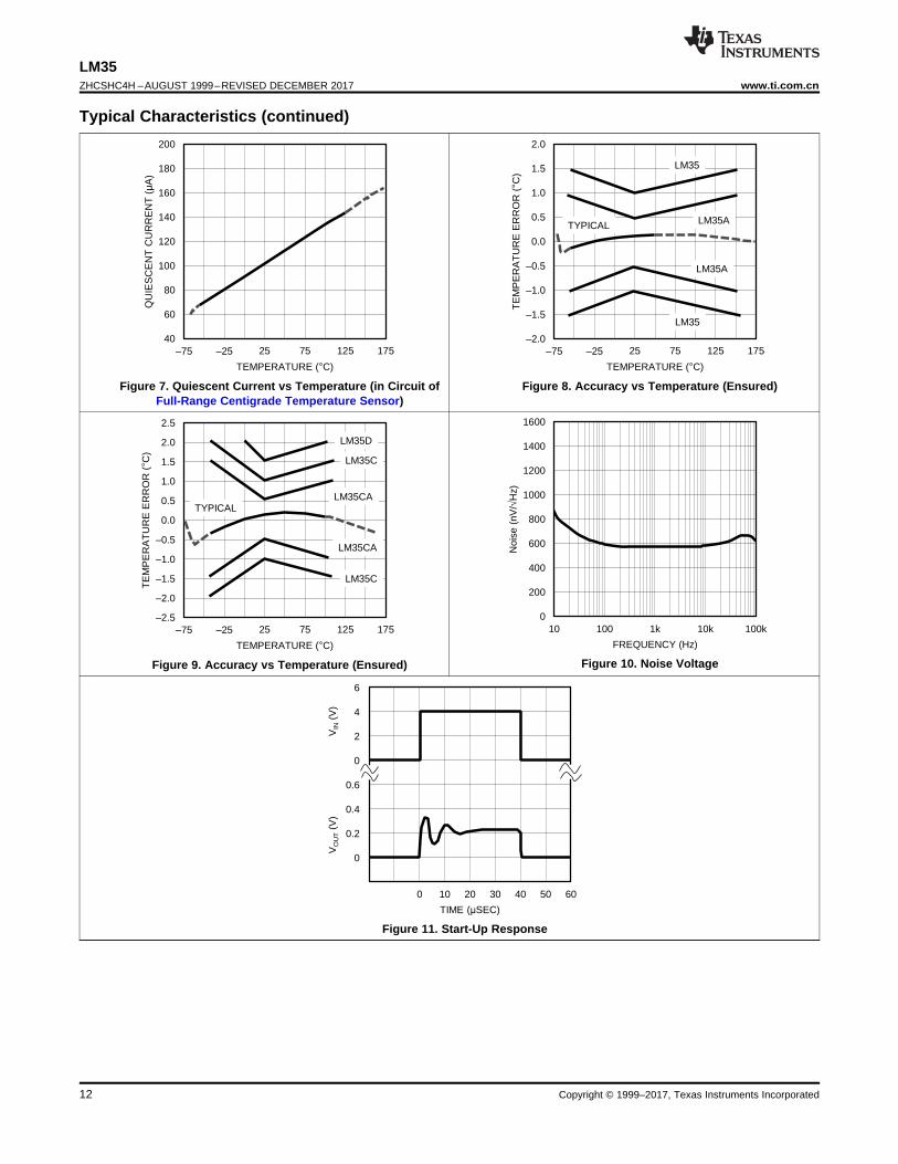
Typical Characteristics (continued)
Figure 7. Quiescent Current vs Temperature (in Circuit ofFull-Range Centigrade Temperature Sensor)
Figure 8. Accuracy vs Temperature (Ensured)
Figure 9. Accuracy vs Temperature (Ensured) Figure 10. Noise Voltage
Figure 11. Start-Up Response

.125 R2
VOUT = 10 mV/°C
+
+VS
R2
A2
A1
V0
nR1
i
8.8 mV/°C
nR1Q1 Q2
10E E
1.38 VPTAT
13
LM35www.ti.com.cn ZHCSHC4H –AUGUST 1999–REVISED DECEMBER 2017
Copyright © 1999–2017, Texas Instruments Incorporated
7 Detailed Description
7.1 OverviewThe LM35-series devices are precision integrated-circuit temperature sensors, with an output voltage linearlyproportional to the Centigrade temperature. The LM35 device has an advantage over linear temperature sensorscalibrated in Kelvin, as the user is not required to subtract a large constant voltage from the output to obtainconvenient Centigrade scaling. The LM35 device does not require any external calibration or trimming to providetypical accuracies of ± ¼ °C at room temperature and ± ¾ °C over a full −55°C to 150°C temperature range.Lower cost is assured by trimming and calibration at the wafer level. The low output impedance, linear output,and precise inherent calibration of the LM35 device makes interfacing to readout or control circuitry especiallyeasy. The device is used with single power supplies, or with plus and minus supplies. As the LM35 device drawsonly 60 μA from the supply, it has very low self-heating of less than 0.1°C in still air. The LM35 device is rated tooperate over a −55°C to 150°C temperature range, while the LM35C device is rated for a −40°C to 110°C range(−10° with improved accuracy). The temperature-sensing element is comprised of a delta-V BE architecture.
The temperature-sensing element is then buffered by an amplifier and provided to the VOUT pin. The amplifierhas a simple class A output stage with typical 0.5-Ω output impedance as shown in the Functional BlockDiagram. Therefore the LM35 can only source current and it's sinking capability is limited to 1 μA.
7.2 Functional Block Diagram
7.3 Feature Description
7.3.1 LM35 Transfer FunctionThe accuracy specifications of the LM35 are given with respect to a simple linear transfer function:
VOUT = 10 mv/°C × T
where• VOUT is the LM35 output voltage• T is the temperature in °C (1)
7.4 Device Functional ModesThe only functional mode of the LM35 is that it has an analog output directly proportional to temperature.

LM35
+
OUT
HEAVY CAPACITIVE LOAD, WIRING, ETC.
TO A HIGH-IMPEDANCE LOAD
v75
1 PF
0.01 PF BYPASSOPTONAL
LM35
+
OUT
2 k
HEAVY CAPACITIVE LOAD, WIRING, ETC.
TO A HIGH-IMPEDANCE LOAD
v
14
LM35ZHCSHC4H –AUGUST 1999–REVISED DECEMBER 2017 www.ti.com.cn
Copyright © 1999–2017, Texas Instruments Incorporated
8 Application and Implementation
NOTEInformation in the following applications sections is not part of the TI componentspecification, and TI does not warrant its accuracy or completeness. TI’s customers areresponsible for determining suitability of components for their purposes. Customers shouldvalidate and test their design implementation to confirm system functionality.
8.1 Application InformationThe features of the LM35 make it suitable for many general temperature sensing applications. Multiple packageoptions expand on it's flexibility.
8.1.1 Capacitive Drive CapabilityLike most micropower circuits, the LM35 device has a limited ability to drive heavy capacitive loads. Alone, theLM35 device is able to drive 50 pF without special precautions. If heavier loads are anticipated, isolating ordecoupling the load with a resistor is easy (see Figure 12). The tolerance of capacitance can be improved with aseries R-C damper from output to ground (see Figure 13).
When the LM35 device is applied with a 200-Ω load resistor as shown in Figure 16, Figure 17, or Figure 19, thedevice is relatively immune to wiring capacitance because the capacitance forms a bypass from ground to inputand not on the output. However, as with any linear circuit connected to wires in a hostile environment,performance is affected adversely by intense electromagnetic sources (such as relays, radio transmitters, motorswith arcing brushes, and SCR transients), because the wiring acts as a receiving antenna and the internaljunctions act as rectifiers. For best results in such cases, a bypass capacitor from VIN to ground and a series R-Cdamper, such as 75 Ω in series with 0.2 or 1 μF from output to ground, are often useful. Examples are shown inFigure 13, Figure 24, and Figure 25.
Figure 12. LM35 with Decoupling from Capacitive Load
Figure 13. LM35 with R-C Damper

±2.0
±1.5
±1.0
±0.5
0.0
0.5
1.0
1.5
2.0
±75 ±25 25 75 125 175
TE
MP
ER
AT
UR
E E
RR
OR
(�C
)
TEMPERATURE (�C) C008
LM35
LM35A
LM35
LM35A TYPICAL
LM35
+VS
(4 V to 20 V)
OUTPUT
0 mV + 10.0 mV/°C
15
LM35www.ti.com.cn ZHCSHC4H –AUGUST 1999–REVISED DECEMBER 2017
Copyright © 1999–2017, Texas Instruments Incorporated
8.2 Typical Application
8.2.1 Basic Centigrade Temperature Sensor
Figure 14. Basic Centigrade Temperature Sensor (2 °C to 150 °C)
8.2.1.1 Design Requirements
Table 1. Design ParametersPARAMETER VALUE
Accuracy at 25°C ±0.5°CAccuracy from –55 °C to 150°C ±1°C
Temperature Slope 10 mV/°C
8.2.1.2 Detailed Design ProcedureBecause the LM35 device is a simple temperature sensor that provides an analog output, design requirementsrelated to layout are more important than electrical requirements. For a detailed description, refer to the Layout.
8.2.1.3 Application Curve
Figure 15. Accuracy vs Temperature (Ensured)

+VS
LM35
18 k
10%
VOUT
+
v
1N914
LM35
+
OUT
VOUT = 10 mV/°C (TAMBIENT = 10 °C)
FROM t 5 °C TO + 40 °C
5 V
200
1%
200
1%
TWISTED PAIR0.01 PF
BYPASSOPTIONAL
2 k
1%
2 k
1%
LM35
+
OUT
VOUT = 10 mV/°C (TAMBIENT = 1 °C)
FROM + 2 °C TO + 40 °C
v
5 V
200
1%
6.8 k
5%
200
1%
TWISTED PAIR
HEAT
FINS
+
v
LM35
+
OUT
VOUT = 10 mV/°C (TAMBIENT = 1 °C)
FROM + 2 °C TO + 40 °C
v
5 V
200
1%
6.8 k
5%
OR 10K RHEOSTAT
FOR GAIN ADJUST
200
1%
TWISTED PAIR
HEAT
FINS
16
LM35ZHCSHC4H –AUGUST 1999–REVISED DECEMBER 2017 www.ti.com.cn
Copyright © 1999–2017, Texas Instruments Incorporated
8.3 System Examples
Figure 16. Two-Wire Remote Temperature Sensor(Grounded Sensor)
Figure 17. Two-Wire Remote Temperature Sensor(Output Referred to Ground)
Figure 18. Temperature Sensor, Single Supply(−55° to +150°C)
Figure 19. Two-Wire Remote Temperature Sensor(Output Referred to Ground)

LM35
9 V
1 k
25.5 kLM385-2.5
100 �A,60 mVFULL-SCALE
LM35
5 V
LM35
+VS
(6 V to 20 V)
45.5 kO
1%
10 kO
1%
26.4 kO
1%
1 MO
1%
18 kOLM385-1.2
VOUT = +1 mV/°F
LM35 LM317
402
1%
50
OUT
OFFSET
ADJUST
+
v
OUT
62.5
0.5%
4.7 k
IN
ADJ
+ 5 V TO + 30 V
2N2907
17
LM35www.ti.com.cn ZHCSHC4H –AUGUST 1999–REVISED DECEMBER 2017
Copyright © 1999–2017, Texas Instruments Incorporated
System Examples (continued)
Figure 20. 4-To-20 mA Current Source(0°C to 100°C)
Figure 21. Fahrenheit Thermometer
Figure 22. Centigrade Thermometer(Analog Meter)
Figure 23. Fahrenheit Thermometer, ExpandedScale Thermometer
(50°F to 80°F, for Example Shown)

LM35
+
OUT
200*
1.5 k*
HEAT
FINS
VA
RA
1 k
1 PF+
20 PF+
LM3914 LM3914
1.2 k*
67 68 69 70 71 72 73 74 75 76 77 78 79 80 81 82 83 84 85 86
10
20 k
18
1 2 3
7 V
4 5 6 7 8 9 1 2 3 4 5 6 7 8 9
NC
VBVC
499*499*
10 18
7 V
7 V
1.5 k*
RC
1 k
1 k*
RB
1 k
20 LEDs
°F
LM35LM131
47
+
GND
8
6 V
100 k
0.01 PF100 k 1 PF
12 k
5 k
FULLSCALEADJ
1 2 4
6
7
0.01 PF
LOW TEMPCO
3
5
1 k6.8 k
4N28
fOUT
LM35
+
OUT
GND
75
1 PF
16 k
ADC0804
+2 k
1 k +
IN
VREF
0.64 V
5 V
8PARALLEL
DATA
OUTPUT
INTR
CS
RD
WR
GND
LM35
+
OUT
GND
75
1 PF
3.9 k
+
10 k
100k+
IN
5 V
SERIAL
DATA OUTPUT
CLOCK
ENABLE
GND
ADC08031
LM385FB
REF
1.28 V
18
LM35ZHCSHC4H –AUGUST 1999–REVISED DECEMBER 2017 www.ti.com.cn
Copyright © 1999–2017, Texas Instruments Incorporated
System Examples (continued)
Figure 24. Temperature to Digital Converter(Serial Output)
(128°C Full Scale)
Figure 25. Temperature to Digital Converter(Parallel TRI-STATE Outputs for Standard Data Bus
to μP Interface)(128°C Full Scale)
*=1% or 2% film resistorTrim RB for VB = 3.075 VTrim RC for VC = 1.955 VTrim RA for VA = 0.075 V + 100 mV/°C ×Tambient
Example, VA = 2.275 V at 22°C
Figure 26. Bar-Graph Temperature Display(Dot Mode)
Figure 27. LM35 With Voltage-To-FrequencyConverter and Isolated Output(2°C to 150°C; 20 to 1500 Hz)

19
LM35www.ti.com.cn ZHCSHC4H –AUGUST 1999–REVISED DECEMBER 2017
Copyright © 1999–2017, Texas Instruments Incorporated
9 Power Supply RecommendationsThe LM35 device has a very wide 4-V to 30-V power supply voltage range, which makes it ideal for manyapplications. In noisy environments, TI recommends adding a 0.1 μF from V+ to GND to bypass the powersupply voltage. Larger capacitances maybe required and are dependent on the power-supply noise.
(1) Wakefield type 201, or 1-in disc of 0.02-in sheet brass, soldered to case, or similar.(2) TO-92 and SOIC-8 packages glued and leads soldered to 1-in square of 1/16-in printed circuit board with 2-oz foil or similar.
10 Layout
10.1 Layout GuidelinesThe LM35 is easily applied in the same way as other integrated-circuit temperature sensors. Glue or cement thedevice to a surface and the temperature should be within about 0.01°C of the surface temperature.
The 0.01°C proximity presumes that the ambient air temperature is almost the same as the surface temperature.If the air temperature were much higher or lower than the surface temperature, the actual temperature of theLM35 die would be at an intermediate temperature between the surface temperature and the air temperature;this is especially true for the TO-92 plastic package. The copper leads in the TO-92 package are the principalthermal path to carry heat into the device, so its temperature might be closer to the air temperature than to thesurface temperature.
Ensure that the wiring leaving the LM35 device is held at the same temperature as the surface of interest tominimize the temperature problem. The easiest fix is to cover up these wires with a bead of epoxy. The epoxybead will ensure that the leads and wires are all at the same temperature as the surface, and that thetemperature of the LM35 die is not affected by the air temperature.
The TO-46 metal package can also be soldered to a metal surface or pipe without damage. Of course, in thatcase the V− terminal of the circuit will be grounded to that metal. Alternatively, mount the LM35 inside a sealed-end metal tube, and then dip into a bath or screw into a threaded hole in a tank. As with any IC, the LM35 deviceand accompanying wiring and circuits must be kept insulated and dry, to avoid leakage and corrosion. This isespecially true if the circuit may operate at cold temperatures where condensation can occur. Printed-circuitcoatings and varnishes such as a conformal coating and epoxy paints or dips are often used to insure thatmoisture cannot corrode the LM35 device or its connections.
These devices are sometimes soldered to a small light-weight heat fin to decrease the thermal time constant andspeed up the response in slowly-moving air. On the other hand, a small thermal mass may be added to thesensor, to give the steadiest reading despite small deviations in the air temperature.
Table 2. Temperature Rise of LM35 Due To Self-heating (Thermal Resistance, RθJA)
TO, no heatsink
TO (1), smallheat fin
TO-92, no heatsink
TO-92 (2), smallheat fin
SOIC-8, noheat sink
SOIC-8 (2),small heat
finTO-220, noheat sink
Still air 400°C/W 100°C/W 180°C/W 140°C/W 220°C/W 110°C/W 90°C/WMoving air 100°C/W 40°C/W 90°C/W 70°C/W 105°C/W 90°C/W 26°C/WStill oil 100°C/W 40°C/W 90°C/W 70°C/W — — —Stirred oil 50°C/W 30°C/W 45°C/W 40°C/W — — —(Clamped tometal, Infiniteheat sink)
(24°C/W) — — (55°C/W) —

VOUT
N.C.
N.C.
+VS
N.C.
0.01 µF
VIA to ground plane
VIA to power plane
GND N.C.
N.C.
20
LM35ZHCSHC4H –AUGUST 1999–REVISED DECEMBER 2017 www.ti.com.cn
版权 © 1999–2017, Texas Instruments Incorporated
10.2 Layout Example
Figure 28. Layout Example

21
LM35www.ti.com.cn ZHCSHC4H –AUGUST 1999–REVISED DECEMBER 2017
版权 © 1999–2017, Texas Instruments Incorporated
11 器器件件和和文文档档支支持持
11.1 接接收收文文档档更更新新通通知知
要接收文档更新通知,请导航至TI.com 上的器件产品文件夹。 点击右上角的提醒我 (Alert me)注册后,即可每周定期收到已更改的产品信息。有关更改的详细信息,请查阅已修订文档中包含的修订历史记录
11.2 社社区区资资源源
下列链接提供到 TI 社区资源的连接。链接的内容由各个分销商“按照原样”提供。这些内容并不构成 TI 技术规范,并且不一定反映 TI 的观点;请参阅 TI 的 《使用条款》。TI E2E™ 在在线线社社区区 TI 的的工工程程师师对对工工程程师师 (E2E) 社社区区。。此社区的创建目的在于促进工程师之间的协作。在
e2e.ti.com 中,您可以咨询问题、分享知识、拓展思路并与同行工程师一道帮助解决问题。设设计计支支持持 TI 参参考考设设计计支支持持可帮助您快速查找有帮助的 E2E 论坛、设计支持工具以及技术支持的联系信息。
11.3 商商标标
E2E is a trademark of Texas Instruments.All other trademarks are the property of their respective owners.
11.4 静静电电放放电电警警告告
这些装置包含有限的内置 ESD 保护。 存储或装卸时,应将导线一起截短或将装置放置于导电泡棉中,以防止 MOS 门极遭受静电损伤。
11.5 GlossarySLYZ022 — TI Glossary.
This glossary lists and explains terms, acronyms, and definitions.
12 机机械械、、封封装装和和可可订订购购信信息息
以下页面包含机械、封装和可订购信息。这些信息是指定器件的最新可用数据。数据如有变更,恕不另行通知和修订此文档。如欲获取此数据表的浏览器版本,请参阅左侧的导航。

PACKAGE OPTION ADDENDUM
www.ti.com 30-Sep-2021
Addendum-Page 1
PACKAGING INFORMATION
Orderable Device Status(1)
Package Type PackageDrawing
Pins PackageQty
Eco Plan(2)
Lead finish/Ball material
(6)
MSL Peak Temp(3)
Op Temp (°C) Device Marking(4/5)
Samples
LM35AH ACTIVE TO NDV 3 500 Non-RoHS &Non-Green
Call TI Call TI -55 to 150 ( LM35AH, LM35AH)
LM35AH/NOPB ACTIVE TO NDV 3 500 RoHS & Green Call TI Level-1-NA-UNLIM -55 to 150 ( LM35AH, LM35AH)
LM35CAH ACTIVE TO NDV 3 500 Non-RoHS &Non-Green
Call TI Call TI -40 to 110 ( LM35CAH, LM35CAH )
LM35CAH/NOPB ACTIVE TO NDV 3 500 RoHS & Green Call TI Level-1-NA-UNLIM -40 to 110 ( LM35CAH, LM35CAH )
LM35CAZ/LFT4 ACTIVE TO-92 LP 3 2000 RoHS & Green SN N / A for Pkg Type LM35CAZ
LM35CAZ/NOPB ACTIVE TO-92 LP 3 1800 RoHS & Green SN N / A for Pkg Type -40 to 110 LM35CAZ
LM35CH ACTIVE TO NDV 3 500 Non-RoHS &Non-Green
Call TI Call TI -40 to 110 ( LM35CH, LM35CH)
LM35CH/NOPB ACTIVE TO NDV 3 500 RoHS & Green Call TI Level-1-NA-UNLIM -40 to 110 ( LM35CH, LM35CH)
LM35CZ/LFT1 ACTIVE TO-92 LP 3 2000 RoHS & Green SN N / A for Pkg Type LM35CZ
LM35CZ/NOPB ACTIVE TO-92 LP 3 1800 RoHS & Green SN N / A for Pkg Type -40 to 110 LM35CZ
LM35DH ACTIVE TO NDV 3 1000 Non-RoHS &Non-Green
Call TI Call TI 0 to 70 ( LM35DH, LM35DH)
LM35DH/NOPB ACTIVE TO NDV 3 1000 RoHS & Green Call TI Level-1-NA-UNLIM 0 to 70 ( LM35DH, LM35DH)
LM35DM NRND SOIC D 8 95 Non-RoHS& Green
Call TI Level-1-235C-UNLIM 0 to 100 LM35DM
LM35DM/NOPB ACTIVE SOIC D 8 95 RoHS & Green SN Level-1-260C-UNLIM 0 to 100 LM35DM
LM35DMX NRND SOIC D 8 2500 Non-RoHS& Green
Call TI Level-1-235C-UNLIM 0 to 100 LM35DM
LM35DMX/NOPB ACTIVE SOIC D 8 2500 RoHS & Green SN Level-1-260C-UNLIM 0 to 100 LM35DM
LM35DT NRND TO-220 NEB 3 45 Non-RoHS& Green
Call TI Level-1-NA-UNLIM 0 to 100 LM35DT

PACKAGE OPTION ADDENDUM
www.ti.com 30-Sep-2021
Addendum-Page 2
Orderable Device Status(1)
Package Type PackageDrawing
Pins PackageQty
Eco Plan(2)
Lead finish/Ball material
(6)
MSL Peak Temp(3)
Op Temp (°C) Device Marking(4/5)
Samples
LM35DT/NOPB ACTIVE TO-220 NEB 3 45 RoHS & Green SN Level-1-NA-UNLIM 0 to 100 LM35DT
LM35DZ/LFT1 ACTIVE TO-92 LP 3 2000 RoHS & Green SN N / A for Pkg Type LM35DZ
LM35DZ/LFT4 ACTIVE TO-92 LP 3 2000 RoHS & Green SN N / A for Pkg Type LM35DZ
LM35DZ/NOPB ACTIVE TO-92 LP 3 1800 RoHS & Green SN N / A for Pkg Type 0 to 100 LM35DZ
LM35H ACTIVE TO NDV 3 500 Non-RoHS &Non-Green
Call TI Call TI -55 to 150 ( LM35H, LM35H)
LM35H/NOPB ACTIVE TO NDV 3 500 RoHS & Green Call TI Level-1-NA-UNLIM -55 to 150 ( LM35H, LM35H)
(1) The marketing status values are defined as follows:ACTIVE: Product device recommended for new designs.LIFEBUY: TI has announced that the device will be discontinued, and a lifetime-buy period is in effect.NRND: Not recommended for new designs. Device is in production to support existing customers, but TI does not recommend using this part in a new design.PREVIEW: Device has been announced but is not in production. Samples may or may not be available.OBSOLETE: TI has discontinued the production of the device.
(2) RoHS: TI defines "RoHS" to mean semiconductor products that are compliant with the current EU RoHS requirements for all 10 RoHS substances, including the requirement that RoHS substancedo not exceed 0.1% by weight in homogeneous materials. Where designed to be soldered at high temperatures, "RoHS" products are suitable for use in specified lead-free processes. TI mayreference these types of products as "Pb-Free".RoHS Exempt: TI defines "RoHS Exempt" to mean products that contain lead but are compliant with EU RoHS pursuant to a specific EU RoHS exemption.Green: TI defines "Green" to mean the content of Chlorine (Cl) and Bromine (Br) based flame retardants meet JS709B low halogen requirements of <=1000ppm threshold. Antimony trioxide basedflame retardants must also meet the <=1000ppm threshold requirement.
(3) MSL, Peak Temp. - The Moisture Sensitivity Level rating according to the JEDEC industry standard classifications, and peak solder temperature.
(4) There may be additional marking, which relates to the logo, the lot trace code information, or the environmental category on the device.
(5) Multiple Device Markings will be inside parentheses. Only one Device Marking contained in parentheses and separated by a "~" will appear on a device. If a line is indented then it is a continuationof the previous line and the two combined represent the entire Device Marking for that device.
(6) Lead finish/Ball material - Orderable Devices may have multiple material finish options. Finish options are separated by a vertical ruled line. Lead finish/Ball material values may wrap to twolines if the finish value exceeds the maximum column width.

PACKAGE OPTION ADDENDUM
www.ti.com 30-Sep-2021
Addendum-Page 3
Important Information and Disclaimer:The information provided on this page represents TI's knowledge and belief as of the date that it is provided. TI bases its knowledge and belief on informationprovided by third parties, and makes no representation or warranty as to the accuracy of such information. Efforts are underway to better integrate information from third parties. TI has taken andcontinues to take reasonable steps to provide representative and accurate information but may not have conducted destructive testing or chemical analysis on incoming materials and chemicals.TI and TI suppliers consider certain information to be proprietary, and thus CAS numbers and other limited information may not be available for release.
In no event shall TI's liability arising out of such information exceed the total purchase price of the TI part(s) at issue in this document sold by TI to Customer on an annual basis.

TAPE AND REEL INFORMATION
*All dimensions are nominal
Device PackageType
PackageDrawing
Pins SPQ ReelDiameter
(mm)
ReelWidth
W1 (mm)
A0(mm)
B0(mm)
K0(mm)
P1(mm)
W(mm)
Pin1Quadrant
LM35DMX SOIC D 8 2500 330.0 12.4 6.5 5.4 2.0 8.0 12.0 Q1
LM35DMX/NOPB SOIC D 8 2500 330.0 12.4 6.5 5.4 2.0 8.0 12.0 Q1
PACKAGE MATERIALS INFORMATION
www.ti.com 5-Jan-2022
Pack Materials-Page 1

*All dimensions are nominal
Device Package Type Package Drawing Pins SPQ Length (mm) Width (mm) Height (mm)
LM35DMX SOIC D 8 2500 367.0 367.0 35.0
LM35DMX/NOPB SOIC D 8 2500 367.0 367.0 35.0
PACKAGE MATERIALS INFORMATION
www.ti.com 5-Jan-2022
Pack Materials-Page 2

TUBE
*All dimensions are nominal
Device Package Name Package Type Pins SPQ L (mm) W (mm) T (µm) B (mm)
LM35DM D SOIC 8 95 495 8 4064 3.05
LM35DM D SOIC 8 95 495 8 4064 3.05
LM35DM/NOPB D SOIC 8 95 495 8 4064 3.05
LM35DM/NOPB D SOIC 8 95 495 8 4064 3.05
LM35DT NEB TO-220 3 45 502 33 6985 4.06
LM35DT NEB TO-220 3 45 502 33 6985 4.06
LM35DT/NOPB NEB TO-220 3 45 502 33 6985 4.06
PACKAGE MATERIALS INFORMATION
www.ti.com 5-Jan-2022
Pack Materials-Page 3

www.ti.com
PACKAGE OUTLINE
C
.228-.244 TYP[5.80-6.19]
.069 MAX[1.75]
6X .050[1.27]
8X .012-.020 [0.31-0.51]
2X.150[3.81]
.005-.010 TYP[0.13-0.25]
0 - 8 .004-.010[0.11-0.25]
.010[0.25]
.016-.050[0.41-1.27]
4X (0 -15 )
A
.189-.197[4.81-5.00]
NOTE 3
B .150-.157[3.81-3.98]
NOTE 4
4X (0 -15 )
(.041)[1.04]
SOIC - 1.75 mm max heightD0008ASMALL OUTLINE INTEGRATED CIRCUIT
4214825/C 02/2019
NOTES: 1. Linear dimensions are in inches [millimeters]. Dimensions in parenthesis are for reference only. Controlling dimensions are in inches. Dimensioning and tolerancing per ASME Y14.5M. 2. This drawing is subject to change without notice. 3. This dimension does not include mold flash, protrusions, or gate burrs. Mold flash, protrusions, or gate burrs shall not exceed .006 [0.15] per side. 4. This dimension does not include interlead flash.5. Reference JEDEC registration MS-012, variation AA.
18
.010 [0.25] C A B
54
PIN 1 ID AREA
SEATING PLANE
.004 [0.1] C
SEE DETAIL A
DETAIL ATYPICAL
SCALE 2.800

www.ti.com
EXAMPLE BOARD LAYOUT
.0028 MAX[0.07]ALL AROUND
.0028 MIN[0.07]ALL AROUND
(.213)[5.4]
6X (.050 )[1.27]
8X (.061 )[1.55]
8X (.024)[0.6]
(R.002 ) TYP[0.05]
SOIC - 1.75 mm max heightD0008ASMALL OUTLINE INTEGRATED CIRCUIT
4214825/C 02/2019
NOTES: (continued) 6. Publication IPC-7351 may have alternate designs. 7. Solder mask tolerances between and around signal pads can vary based on board fabrication site.
METALSOLDER MASKOPENING
NON SOLDER MASKDEFINED
SOLDER MASK DETAILS
EXPOSEDMETAL
OPENINGSOLDER MASK METAL UNDER
SOLDER MASK
SOLDER MASKDEFINED
EXPOSEDMETAL
LAND PATTERN EXAMPLEEXPOSED METAL SHOWN
SCALE:8X
SYMM
1
45
8
SEEDETAILS
SYMM

www.ti.com
EXAMPLE STENCIL DESIGN
8X (.061 )[1.55]
8X (.024)[0.6]
6X (.050 )[1.27]
(.213)[5.4]
(R.002 ) TYP[0.05]
SOIC - 1.75 mm max heightD0008ASMALL OUTLINE INTEGRATED CIRCUIT
4214825/C 02/2019
NOTES: (continued) 8. Laser cutting apertures with trapezoidal walls and rounded corners may offer better paste release. IPC-7525 may have alternate design recommendations. 9. Board assembly site may have different recommendations for stencil design.
SOLDER PASTE EXAMPLEBASED ON .005 INCH [0.125 MM] THICK STENCIL
SCALE:8X
SYMM
SYMM
1
45
8


www.ti.com
PACKAGE OUTLINE
3X 2.672.03
5.214.44
5.344.32
3X12.7 MIN
2X 1.27 0.13
3X 0.550.38
4.193.17
3.43 MIN
3X 0.430.35
(2.54)NOTE 3
2X2.6 0.2
2X4 MAX
SEATINGPLANE
6X0.076 MAX
(0.51) TYP
(1.5) TYP
TO-92 - 5.34 mm max heightLP0003ATO-92
4215214/B 04/2017
NOTES: 1. All linear dimensions are in millimeters. Any dimensions in parenthesis are for reference only. Dimensioning and tolerancing per ASME Y14.5M.2. This drawing is subject to change without notice.3. Lead dimensions are not controlled within this area.4. Reference JEDEC TO-226, variation AA.5. Shipping method: a. Straight lead option available in bulk pack only. b. Formed lead option available in tape and reel or ammo pack. c. Specific products can be offered in limited combinations of shipping medium and lead options. d. Consult product folder for more information on available options.
EJECTOR PINOPTIONAL
PLANESEATING
STRAIGHT LEAD OPTION
3 2 1
SCALE 1.200
FORMED LEAD OPTIONOTHER DIMENSIONS IDENTICAL
TO STRAIGHT LEAD OPTION
SCALE 1.200

www.ti.com
EXAMPLE BOARD LAYOUT
0.05 MAXALL AROUND
TYP
(1.07)
(1.5) 2X (1.5)
2X (1.07)(1.27)
(2.54)
FULL RTYP
( 1.4)0.05 MAXALL AROUND
TYP
(2.6)
(5.2)
(R0.05) TYP
3X ( 0.9) HOLE
2X ( 1.4)METAL
3X ( 0.85) HOLE
(R0.05) TYP
4215214/B 04/2017
TO-92 - 5.34 mm max heightLP0003ATO-92
LAND PATTERN EXAMPLEFORMED LEAD OPTIONNON-SOLDER MASK DEFINED
SCALE:15X
SOLDER MASKOPENING
METAL
2XSOLDER MASKOPENING
1 2 3
LAND PATTERN EXAMPLESTRAIGHT LEAD OPTIONNON-SOLDER MASK DEFINED
SCALE:15X
METALTYP
SOLDER MASKOPENING
2XSOLDER MASKOPENING
2XMETAL
1 2 3
www.ti.com
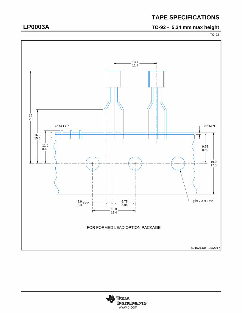
TAPE SPECIFICATIONS
19.017.5
13.711.7
11.08.5
0.5 MIN
TYP-4.33.7
9.758.50
TYP2.92.4
6.755.95
13.012.4
(2.5) TYP
16.515.5
3223
4215214/B 04/2017
TO-92 - 5.34 mm max heightLP0003ATO-92
FOR FORMED LEAD OPTION PACKAGE

www.ti.com
PACKAGE OUTLINE
( 2.54)1.160.92
4.954.55
0.76 MAX 2.67 MAX
0.64 MAXUNCONTROLLEDLEAD DIA
3X12.7 MIN
3X 0.4830.407
-5.565.32
1.220.72
45
TO-CAN - 2.67 mm max heightNDV0003HTO-46
4219876/A 01/2017
NOTES: 1. All linear dimensions are in millimeters. Any dimensions in parenthesis are for reference only. Dimensioning and tolerancing per ASME Y14.5M.2. This drawing is subject to change without notice.3. Reference JEDEC registration TO-46.
1
2
3
SCALE 1.250

www.ti.com
EXAMPLE BOARD LAYOUT
0.07 MAXALL AROUND
0.07 MAXTYP
( 1.2)METAL
2X ( 1.2) METAL
3X ( 0.7) VIA
(R0.05) TYP
(2.54)
(1.27)
TO-CAN - 2.67 mm max heightNDV0003HTO-46
4219876/A 01/2017
LAND PATTERN EXAMPLENON-SOLDER MASK DEFINED
SCALE:12X
2XSOLDER MASKOPENING
SOLDER MASKOPENING
1
2
3

重要声明和免责声明TI“按原样”提供技术和可靠性数据(包括数据表)、设计资源(包括参考设计)、应用或其他设计建议、网络工具、安全信息和其他资源,不保证没有瑕疵且不做出任何明示或暗示的担保,包括但不限于对适销性、某特定用途方面的适用性或不侵犯任何第三方知识产权的暗示担保。这些资源可供使用 TI 产品进行设计的熟练开发人员使用。您将自行承担以下全部责任:(1) 针对您的应用选择合适的 TI 产品,(2) 设计、验证并测试您的应用,(3) 确保您的应用满足相应标准以及任何其他功能安全、信息安全、监管或其他要求。这些资源如有变更,恕不另行通知。TI 授权您仅可将这些资源用于研发本资源所述的 TI 产品的应用。严禁对这些资源进行其他复制或展示。您无权使用任何其他 TI 知识产权或任何第三方知识产权。您应全额赔偿因在这些资源的使用中对 TI 及其代表造成的任何索赔、损害、成本、损失和债务,TI 对此概不负责。TI 提供的产品受 TI 的销售条款或 ti.com 上其他适用条款/TI 产品随附的其他适用条款的约束。TI 提供这些资源并不会扩展或以其他方式更改 TI 针对 TI 产品发布的适用的担保或担保免责声明。TI 反对并拒绝您可能提出的任何其他或不同的条款。IMPORTANT NOTICE
邮寄地址:Texas Instruments, Post Office Box 655303, Dallas, Texas 75265Copyright © 2022,德州仪器 (TI) 公司